Mini Hi-Fi SystemSERVICE MANUAL
MODEL: RAT375 (RAS375F/W)
CAUTIONBEFORE SERVICING THE UNIT, READ THE “SAFETY PRECAUTIONS”IN THIS MANUAL.
MO
DE
L: R
AT
375 (RA
S375F
/W)
SE
RV
ICE
MA
NU
AL
P/NO : AFN73972613 MARCH, 2010
Website http://biz.lgservice.comInternal Use Only
1-1
[CONTENTS]
SECTION 1. GENERAL • SERVICING PRECAUTIONS . . . . . . . . . . . . . . . . . . . . . . . . . . . . . . . . . . . . . . . . . . . . . . . . . 1-2
• ESD PRECAUTIONS . . . . . . . . . . . . . . . . . . . . . . . . . . . . . . . . . . . . . . . . . . . . . . . . . . . . . . . 1-4
• SERVICE INFORMATION FOR EEPROM . . . . . . . . . . . . . . . . . . . . . . . . . . . . . . . . . . . . . . 1-5
• PROGRAM DOWNLOAD GUIDE . . . . . . . . . . . . . . . . . . . . . . . . . . . . . . . . . . . . . . . . . . . . . . . . . . . . . . . . . . . 1-6
• SPECIFICATIONS . . . . . . . . . . . . . . . . . . . . . . . . . . . . . . . . . . . . . . . . . . . . . . . . . . . . . . . . . 1-8
SECTION 2. EXPLODED VIEWS . . . . . . . . . . . . . . . . . . . . . . . . . . . . . . . . . . . . . . . . . . . . . 2-1
• CABINET AND MAIN FRAME SECTION . . . . . . . . . . . . . . . . . . . . . . . . . . . . . . . . . . . . . . . . 2-1
• MECHANISM DECK SECTION (CDM-345) . . . . . . . . . . . . . . . . . . . . . . . . . . . . . . . . . . . . . . 2-3
• SPEAKER SECTION . . . . . . . . . . . . . . . . . . . . . . . . . . . . . . . . . . . . . . . . . . . . . . . . . . . . . . . 2-5
• PACKING ACCESSORY SECTION . . . . . . . . . . . . . . . . . . . . . . . . . . . . . . . . . . . . . . . . . . . . 2-7
SECTION 3. ELECTRICAL PART • TROUBLESHOOTING GUIDE . . . . . . . . . . . . . . . . . . . . . . . . . . . . . . . . . . . . . . . . . . . . . . . . 3-1
• DETAILS AND WAVEFORMS ON SYSTEM TEST AND DEBUGGING . . . . . . . . . . . . . . . 3-14
• WIRING DIAGRAM . . . . . . . . . . . . . . . . . . . . . . . . . . . . . . . . . . . . . . . . . . . . . . . . . . . . . . . 3-18
• BLOCK DIAGRAMS . . . . . . . . . . . . . . . . . . . . . . . . . . . . . . . . . . . . . . . . . . . . . . . . . . . . . . 3-19
• CIRCUIT DIAGRAMS . . . . . . . . . . . . . . . . . . . . . . . . . . . . . . . . . . . . . . . . . . . . . . . . . . . . . . 3-21
• CIRCUIT VOLTAGE CHART . . . . . . . . . . . . . . . . . . . . . . . . . . . . . . . . . . . . . . . . . . . . . . . . 3-33
• PRINTED CIRCUIT DIARGAMS . . . . . . . . . . . . . . . . . . . . . . . . . . . . . . . . . . . . . . . . . . . . . 3-35
SECTION 4. REPLACEMENT PARTS LIST . . . . . . . . . . . . . . . . . . . . . . . . . . . . . . . . . . . 4-1

1-2
SERVICING PRECAUTIONSNOTES REGARDING HANDLING OF THE PICK-UP1. Notes for transport and storage
1) The pick-up should always be left in its conductive bag until immediately prior to use.2) The pick-up should never be subjected to external pressure or impact.
2. Repair notes
1) The pick-up incorporates a strong magnet, and so should never be brought close to magnetic materials.2) The pick-up should always be handled correctly and carefully, taking care to avoid external pressure and
impact. If it is subjected to strong pressure or impact, the result may be an operational malfunction and/or damage to the printed-circuit board.
3) Each and every pick-up is already individually adjusted to a high degree of precision, and for that reason the adjustment point and installation screws should absolutely never be touched.
4) Laser beams may damage the eyes!Absolutely never permit laser beams to enter the eyes!Also NEVER switch ON the power to the laser output part (lens, etc.) of the pick-up if it is damaged.
5) Cleaning the lens surfaceIf there is dust on the lens surface, the dust should be cleaned away by using an air bush (such as used for camera lens). The lens is held by a delicate spring. When cleaning the lens surface, therefore, a cot-ton swab should be used, taking care not to distort lens.
6) Never attempt to disassemble the pick-up.Spring has excess pressure. If the lens is extremely dirty, apply isopropyl alcohol to the cotton swab. (Do not use any other liquid cleaners, because they will damage the lens.) Take care not to use too much of this alcohol on the swab, and do not allow the alcohol to get inside the pick-up.
Storage in conductive bag Drop impact
NEVER look directly at the laser beam, and don’t allow contact with fingers or other exposed skin.
Magnet
How to hold the pick-up
Conductive Sheet
Cotton swab
Pressure
Pressure
SECTION 1. GENERAL
1-3
NOTES REGARDING COMPACT DISC PLAYER REPAIRS1. Preparations1) Compact disc players incorporate a great many ICs as well as the pick-up (laser diode). These components
are sensitive to, and easily affected by, static electricity. If such static electricity is high voltage, components can be damaged, and for that reason components should be handled with care.
2) The pick-up is composed of many optical components and other high-precision components. Care must be taken, therefore, to avoid repair or storage where the temperature or humidity is high, where strong magne-tism is present, or where there is excessive dust.
2. Notes for repair1) Before replacing a component part, first disconnect the power supply lead wire from the unit2) All equipment, measuring instruments and tools must be grounded.3) The workbench should be covered with a conductive sheet and grounded.
When removing the laser pick-up from its conductive bag, do not place the pick-up on the bag. (This is because there is the possibility of damage by static electricity.)
4) To prevent AC leakage, the metal part of the soldering iron should be grounded.5) Workers should be grounded by an armband (1 MΩ)6) Care should be taken not to permit the laser pick-up to come in contact with clothing, in order to prevent
static electricity changes in the clothing to escape from the armband.
7) The laser beam from the pick-up should NEVER be directly facing the eyes or bare skin.
Resistor(1 MΩ) Conductive
Sheet
Resistor(1 MΩ)
Armband

1-4
ESD PRECAUTIONS
Electrostatically Sensitive Devices (ESD)Some semiconductor (solid state) devices can be damaged easily by static electricity. Such componentscommonly are called Electrostatically Sensitive Devices (ESD). Examples of typical ESD devices are integratedcircuits and some field-effect transistors and semiconductor chip components. The following techniques shouldbe used to help reduce the incidence of component damage caused by static electricity.
1. Immediately before handling any semiconductor component or semiconductor-equipped assembly, drain offany electrostatic charge on your body by touching a known earth ground. Alternatively, obtain and wear acommercially available discharging wrist strap device, which should be removed for potential shock reasonsprior to applying power to the unit under test.
2. After removing an electrical assembly equipped with ESD devices, place the assembly on a conductive surface such as aluminum foil, to prevent electrostatic charge buildup or exposure of the assembly.
3. Use only a grounded-tip soldering iron to solder or unsolder ESD devices.
4. Use only an anti-static solder removal device. Some solder removal devices not classified as "anti-static" can generate electrical charges sufficient to damage ESD devices.
5. Do not use freon-propelled chemicals. These can generate electrical charges sufficient to damage ESDdevices.
6. Do not remove a replacement ESD device from its protective package until immediately before you areready to install it. (Most replacement ESD devices are packaged with leads electrically shorted together byconductive foam, aluminum foil or comparable conductive materials).
7. Immediately before removing the protective material from the leads of a replacement ESD device, touch theprotective material to the chassis or circuit assembly into which the device will by installed.
CAUTION : BE SURE NO POWER IS APPLIED TO THE CHASSIS OR CIRCUIT, AND OBSERVE ALL OTHER SAFETY PRECAUTIONS.
8. Minimize bodily motions when handing unpackaged replacement ESD devices. (Otherwise harmless motionsuch as the brushing together of your clothes fabric or the lifting of your foot from a carpeted floor can generate static electricity sufficient to damage an ESD device).
CAUTION. GRAPHIC SYMBOLS
THE LIGHTNING FLASH WITH APROWHEAD SYMBOL. WITHIN AN EQUILATERAL TRIANGLE, IS INTENDED TO ALERT THE SERVICE PERSONNEL TO THE PRESENCE OF UNINSULATED “DANGEROUS VOLTAGE” THAT MAY BE OF SUFFICIENT MAGNITUDE TO CONSTITUTE A RISK OF ELECTRIC SHOCK.
THE EXCLAMATION POINT WITHIN AN EQUILATERAL TRIANGLE IS INTENDED TO ALERT THESERVICE PERSONNEL TO THE PRESENCE OF IMPORTANT SAFETY INFORMATION IN SERVICELITERATURE.
1-5
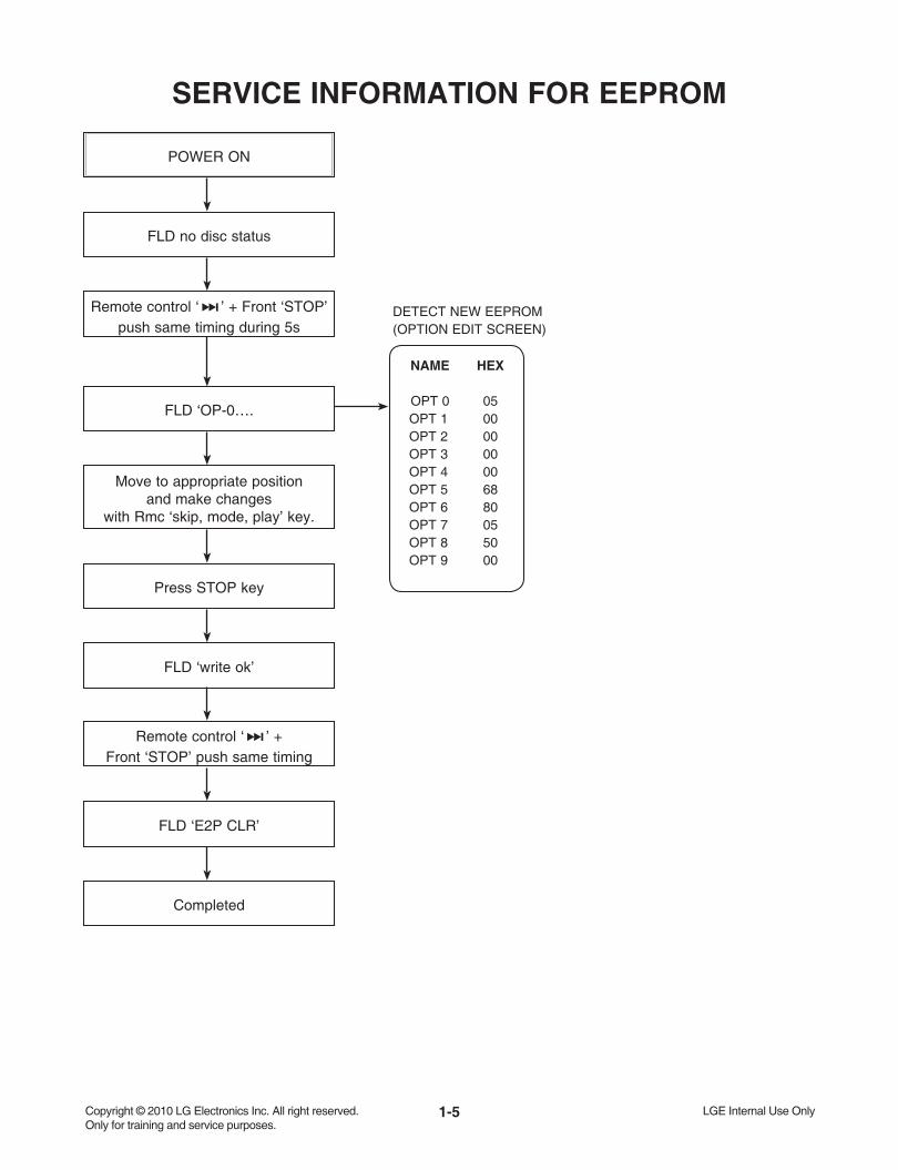
SERVICE INFORMATION FOR EEPROM
POWER ON
FLD no disc status
Remote control ‘ ’ + Front ‘STOP’push same timing during 5s
FLD ‘OP-0….
Move to appropriate positionand make changes
with Rmc ‘skip, mode, play’ key.
Press STOP key
FLD ‘write ok’
Remote control ‘ ’ +Front ‘STOP’ push same timing
FLD ‘E2P CLR’
Completed
NAME
OPT 0OPT 1OPT 2OPT 3OPT 4OPT 5OPT 6OPT 7OPT 8OPT 9
DETECT NEW EEPROM(OPTION EDIT SCREEN)
HEX
05000000006880055000
1-6
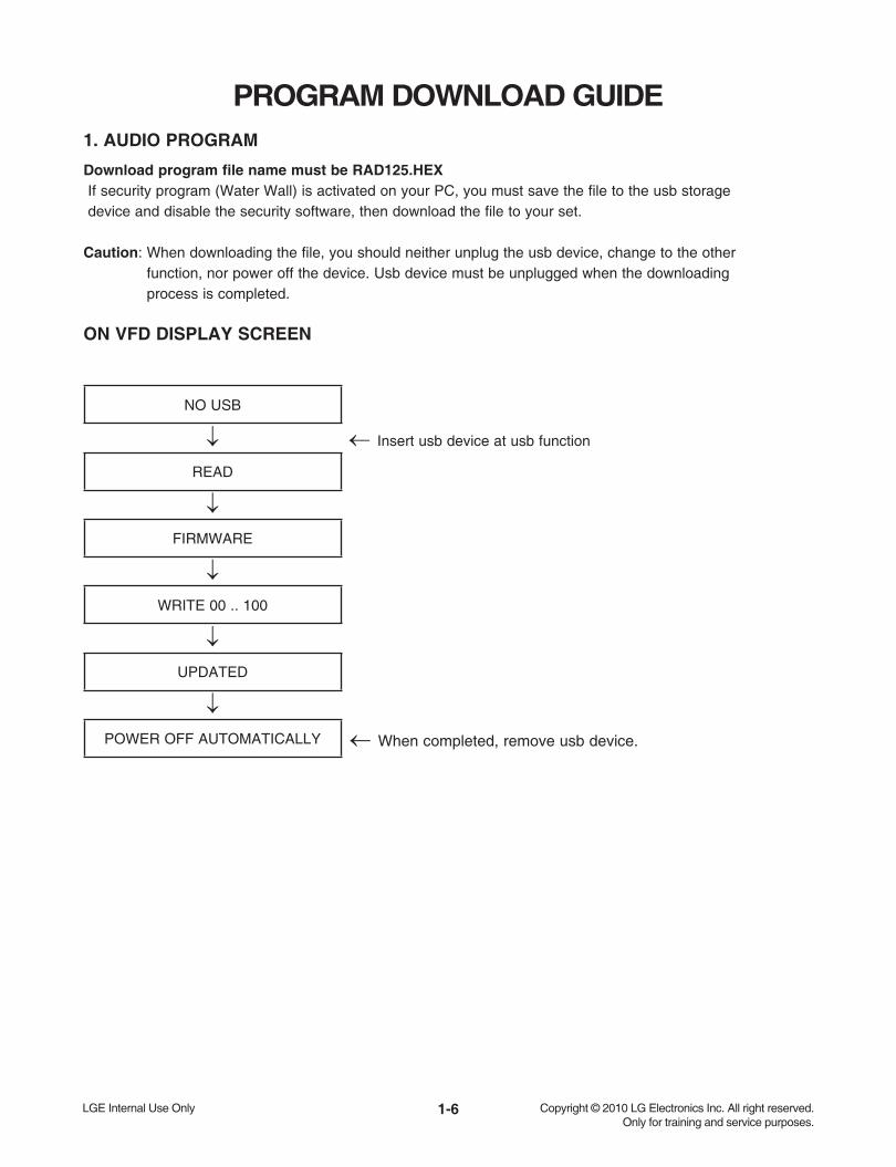
PROGRAM DOWNLOAD GUIDE1. AUDIO PROGRAM
Download program file name must be RAD125.HEX If security program (Water Wall) is activated on your PC, you must save the file to the usb storagedevice and disable the security software, then download the file to your set.
Caution: When downloading the file, you should neither unplug the usb device, change to the otherfunction, nor power off the device. Usb device must be unplugged when the downloadingprocess is completed.
ON VFD DISPLAY SCREEN
NO USB
↓ ← Insert usb device at usb function
READ
↓FIRMWARE
↓WRITE 00 .. 100
↓UPDATED
↓POWER OFF AUTOMATICALLY ← When completed, remove usb device.
1-7
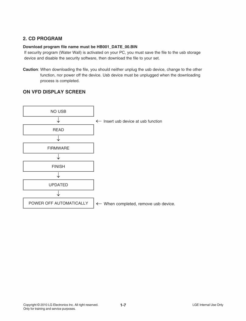
2. CD PROGRAM
Download program file name must be HB001_DATE_00.BIN If security program (Water Wall) is activated on your PC, you must save the file to the usb storagedevice and disable the security software, then download the file to your set.
Caution: When downloading the file, you should neither unplug the usb device, change to the otherfunction, nor power off the device. Usb device must be unplugged when the downloadingprocess is completed.
ON VFD DISPLAY SCREEN
NO USB
↓ ← Insert usb device at usb function
READ
↓FIRMWARE
↓FINISH
↓UPDATED
↓POWER OFF AUTOMATICALLY ← When completed, remove usb device.
1-8
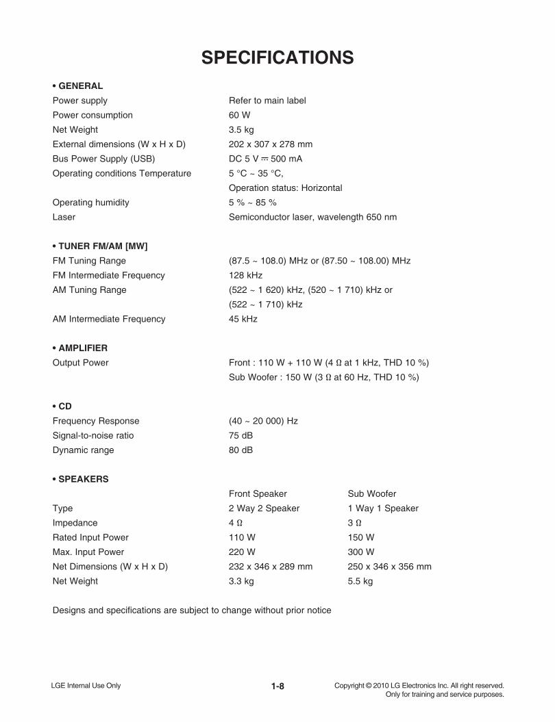
SPECIFICATIONS• GENERAL
Power supply Refer to main label
Power consumption 60 W
Net Weight 3.5 kg
External dimensions (W x H x D) 202 x 307 x 278 mm
Bus Power Supply (USB) DC 5 V 500 mA
Operating conditions Temperature 5 °C ~ 35 °C,
Operation status: Horizontal
Operating humidity 5 % ~ 85 %
Laser Semiconductor laser, wavelength 650 nm
• TUNER FM/AM [MW]
FM Tuning Range (87.5 ~ 108.0) MHz or (87.50 ~ 108.00) MHz
FM Intermediate Frequency 128 kHz
AM Tuning Range (522 ~ 1 620) kHz, (520 ~ 1 710) kHz or
(522 ~ 1 710) kHz
AM Intermediate Frequency 45 kHz
• AMPLIFIER
Output Power Front : 110 W + 110 W (4 Ω at 1 kHz, THD 10 %)
Sub Woofer : 150 W (3 Ω at 60 Hz, THD 10 %)
• CD
Frequency Response (40 ~ 20 000) Hz
Signal-to-noise ratio 75 dB
Dynamic range 80 dB
• SPEAKERS
Front Speaker Sub Woofer
Type 2 Way 2 Speaker 1 Way 1 Speaker
Impedance 4 Ω 3 Ω
Rated Input Power 110 W 150 W
Max. Input Power 220 W 300 W
Net Dimensions (W x H x D) 232 x 346 x 289 mm 250 x 346 x 356 mm
Net Weight 3.3 kg 5.5 kg
Designs and specifications are subject to change without prior notice

D
H
G
C
CF
E
B
A
F
EH
G
D
A
B
FRONT
USB
SMPS
I
258C
255L
260L
256L 255R
256R
258B
258A
251
253
252
250
254
460
460
261 460
460
264
451
A47
276
265259
A26
460
460
A46
300
460
460
273 274
460
279460
460
262
460
257
CABLE2
260R
A43
A44
A42
460
I
SECTION 2. EXPLODED VIEWS • CABINET AND MAIN FRAME SECTION (RAT375)
2-1 2-2
NOTES) THE EXCLAMATION POINT WITHIN AN EQUILATERAL TRIANGLE IS INTENDED TO ALERT THE SERVICE PERSONNEL TO THE PRESENCE OF IMPORTANT SAFETY INFORMATION IN SERVICELITERATURE.

2-3 2-4
• MECHANISM DECK SECTION (CDM-345)
018
439
014013
017
019
026
015
431
020
A01
A02 001
002
003
016036
010
012
012A
012A
012
432
432
037A03
A26
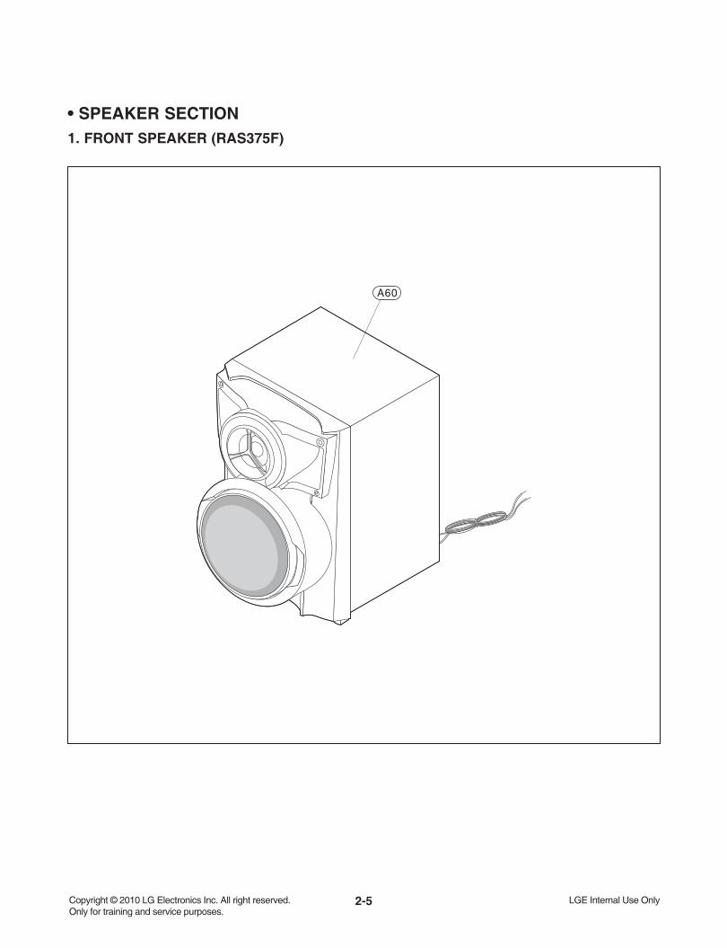
2-5
A60
• SPEAKER SECTION1. FRONT SPEAKER (RAS375F)
2-6
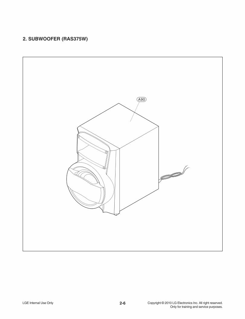
2. SUBWOOFER (RAS375W)
A90
2-7
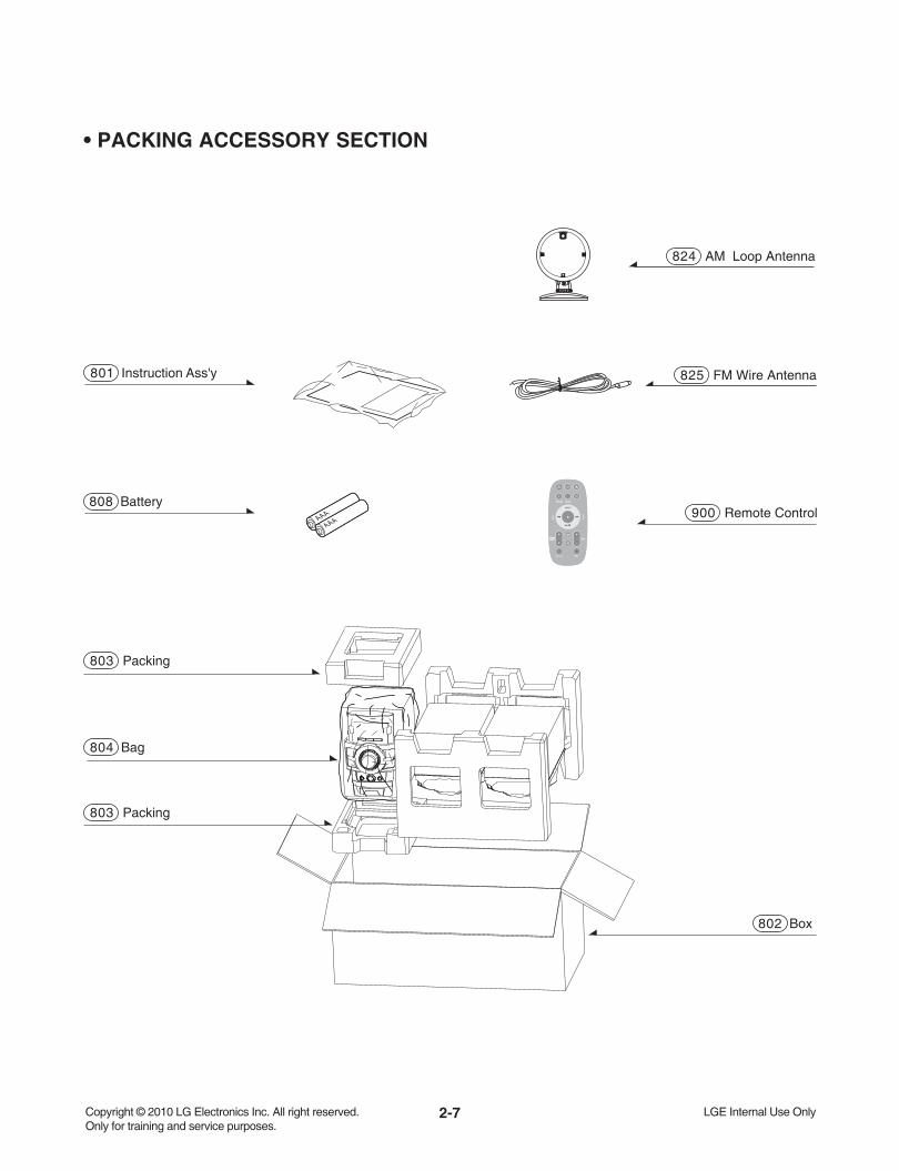
• PACKING ACCESSORY SECTION
825 FM Wire Antenna
900 Remote Control
803 Packing
803 Packing
808 Battery
802 Box
801 Instruction Ass'y
804 Bag
824 AM Loop Antenna
2-8
MEMO

3-1
SECTION 3. ELECTRICAL PARTAUDIO ELECTRICAL TROUBLESHOOTIHG GUIDE
1. POWER (SMPS)
No 3.7 VA
YES
Is F901 normal? Replace the F901 (Use the same fuse).
YES
NO
Is BD901 normal? Replace BD901.
YES
NO
Is TH902 normal? Replace TH902.
YES
NO
Is Vcc(10 V ~ 18 V) supplied to
IC901 Pin7?Is D904 normal?
YES
NO
Check or replace D904.
Is thereabout 2.5 V atIC903 Pin1?
Replace IC903.
YES
NO
Is D923 normal? Replace D923.
YES
NO
Is D921 normal? Replace D921.
YES
NO
Is D924 normal? Replace D924.
YES
NO
Is D925 normal? Replace D925.
YES
NO
Is D922 normal? Replace D922.
YES
NO
Power line of I/O PCB is short.
NO
3-2
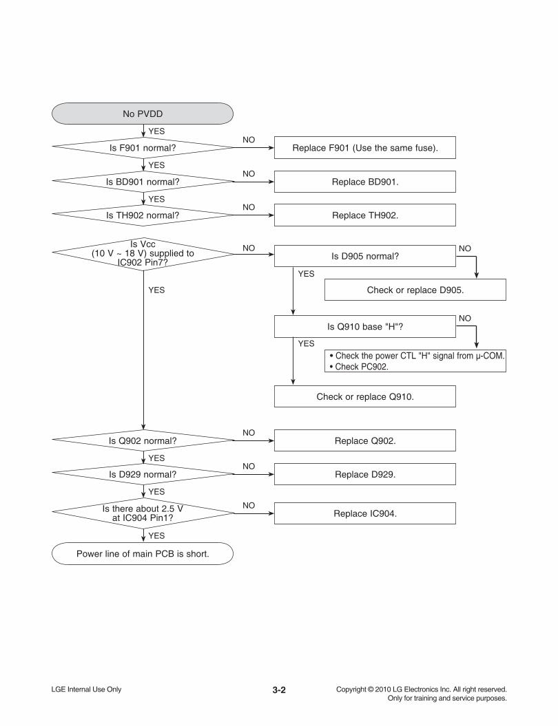
No PVDD
YES
Is F901 normal? Replace F901 (Use the same fuse).
YES
NO
Is BD901 normal? Replace BD901.
YES
NO
Is TH902 normal? Replace TH902.
YES
YES
NO
Is Vcc(10 V ~ 18 V) supplied to
IC902 Pin7?Is D905 normal?
YES
NO
Check or replace D905.
• Check the power CTL "H" signal from μ-COM. • Check PC902.
Is Q902 normal? Replace Q902.
Check or replace Q910.
YES
NO
Is D929 normal? Replace D929.
YES
NO
Is there about 2.5 V at IC904 Pin1? Replace IC904.
YES
NO
Is Q910 base "H"?
Power line of main PCB is short.
NO
NO

3-3
No 12 V
Is Vcc(15 V) supplied to Q953
collector?Check or replace D921.
YES
YES
NO
Is the 13 V Supplied to Q953
base?
Check the power CTL “H” signal from μ-COM.
YES
NO
Check or replace Q953.
No 5 V
Is Vcc(6 V) supplied to IC951
Pin1?Check or replace D923.
YES
YES
NO
CheckIC951 Pin4 "H".
Check the power CTL“H”’ signal from μ-COM.
YES
NO
Check or replace IC951.

3-4
2. μ-COM PART CHECK I
YES
μ-COM PART CHECK I
Check P-SENS CN105
Pin9,10(3.7 VA).
Checkif input voltage of
IC101 is over3.7 V.
Check both end voltage of IC105
(KIA7027).
Refer to SMPS troubleshooting.
NO
NO
Check voltage of IC102(LC87Fxxx) Pin59,36.
Check the periphery of IC105 (KIA7027).
NO Replace IC105(KIA7027).
NO
Check if IC105 voltage is over 3.5 V.
OK OK
YES
YES
YES
YES
YES
No VFD
Is D925 normal? Check or replace D925.
YES
YES
NO
Is ZD951 normal?
Is Q951 normal?
Check or replace ZD951.
Check or replace Q951.
YES
YES
NO
NO
Check or replace VFD.
3-5
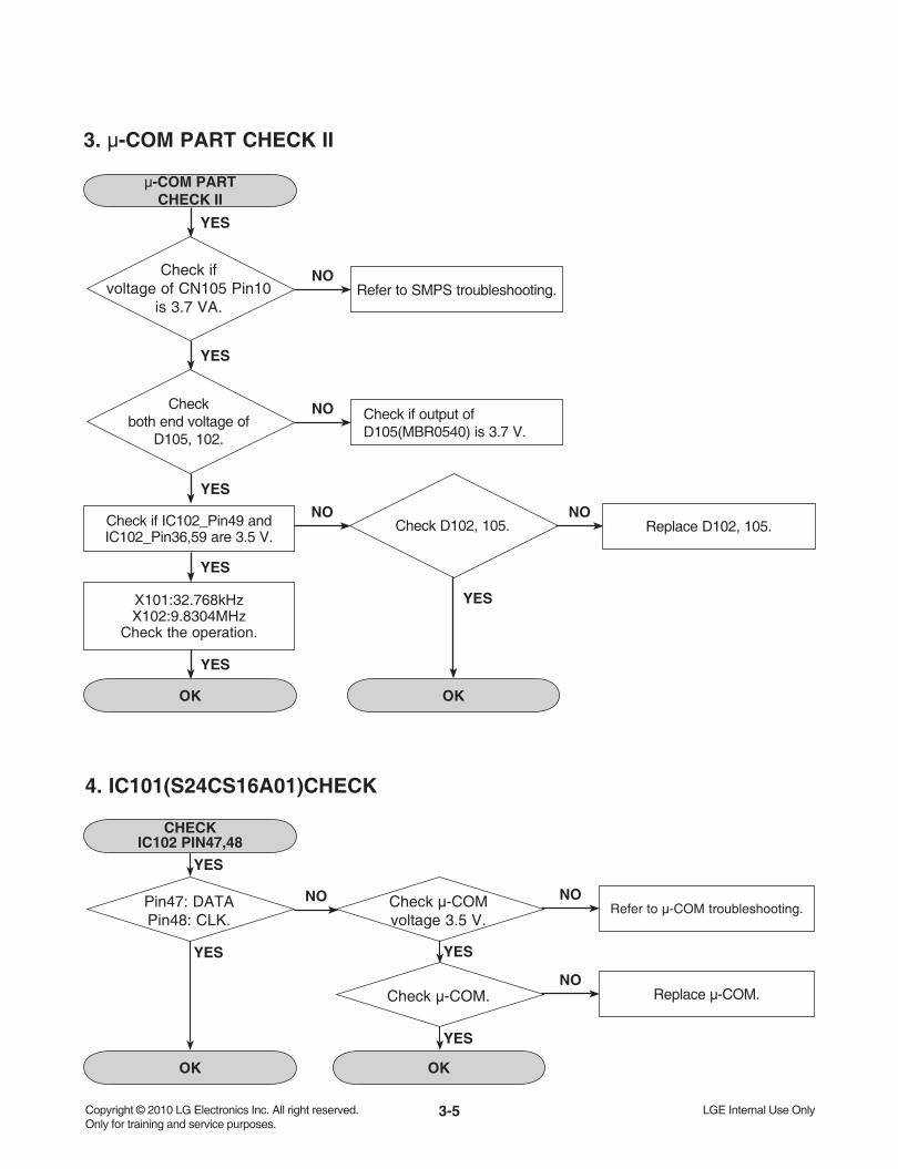
3. μ-COM PART CHECK II
μ-COM PART CHECK II
Refer to SMPS troubleshooting.NOCheck if
voltage of CN105 Pin10is 3.7 VA.
Check if output of D105(MBR0540) is 3.7 V.
NOCheckboth end voltage of
D105, 102.
Check if IC102_Pin49 and IC102_Pin36,59 are 3.5 V.
YES
Check D102, 105. Replace D102, 105.NONO
X101:32.768kHzX102:9.8304MHz
Check the operation.
OK
YES
YES
YES
YES
YES
OK
4. IC101(S24CS16A01)CHECK
CHECKIC102 PIN47,48
Refer to μ-COM troubleshooting.NOPin47: DATA
Pin48: CLK.
Replace μ-COM. NO
YES
Check μ-COMvoltage 3.5 V.
Check μ-COM.
YES
OK OK
YES
YES
NO

3-6
5. FLD DISPLAY CHECK
FLD DISPLAY CHECK
OK
YES
CheckCN104 Pin1,2,3 input
voltage.
YES
Check if both end voltage of F1,F2 are over 3.4 V VKK : over 26 V.
NORefer to SMPS troubleshooting.
YES
Check CN304connection and power
Pin14,15,16(VKK,FL-,FL+),Pin11(3.7 VA).
YES
OK
NOCheck CN304 connection.
YES
Check eachPin voltage.
YES
CheckIC501(ET6315) voltage
Pin30 VKK:-26 VPin13, 43:+5 V.
YES
Check IC102->IC501
data communication 3Pin->9Pin STB2Pin->7Pin DATA4Pin->8Pin CLK
FLD light on?
OK
NO If voltage is Not 3.7 VA,check input and output of D501.
YES
Check IC501.
YES
NOReplace IC501.
NO Check input data IC102 Pin2,3,4.
YES
OK
Check IC102
YES
NOReplace IC102.
Check output data IC102 Pin2.
YESYES
YES
3-7
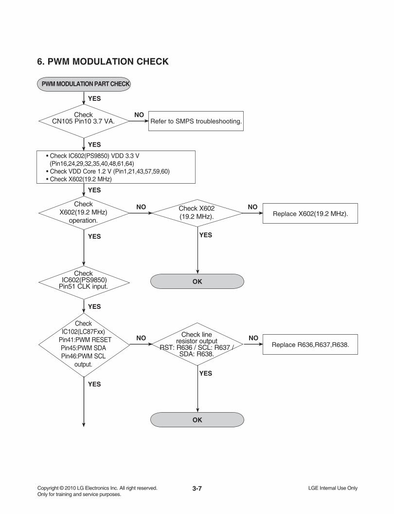
6. PWM MODULATION CHECK
PWM MODULATION PART CHECK
CheckCN105 Pin10 3.7 VA.
• Check IC602(PS9850) VDD 3.3 V (Pin16,24,29,32,35,40,48,61,64) • Check VDD Core 1.2 V (Pin1,21,43,57,59,60)• Check X602(19.2 MHz)
NORefer to SMPS troubleshooting.
CheckX602(19.2 MHz)
operation.
NOReplace X602(19.2 MHz).
Check X602(19.2 MHz).
OK
YES
NO
Check IC602(PS9850)Pin51 CLK input.
CheckIC102(LC87Fxx)
Pin41:PWM RESETPin45:PWM SDA Pin46:PWM SCL
output.
NOReplace R636,R637,R638.
Check lineresistor output
RST: R636 / SCL: R637 /SDA: R638.
NO
YES
YES
YES
YES
YES
YES
OK
YES
3-8
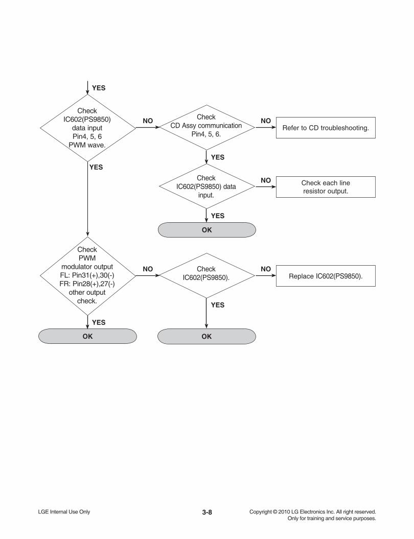
OK
CheckIC602(PS9850)
data inputPin4, 5, 6
PWM wave.
NORefer to CD troubleshooting.
CheckCD Assy communication
Pin4, 5, 6.
OK
NO
NO Check each line resistor output.
CheckIC602(PS9850) data
input.
CheckPWM
modulator outputFL: Pin31(+),30(-)FR: Pin28(+),27(-)
other outputcheck.
NOReplace IC602(PS9850).
CheckIC602(PS9850).
NO
OK
YES
YES
YES
YES
YES
YES

3-9
7. POWER AMP PART CHECK
POWER AMP PART CHECK
Refer to SMPS troubleshooting.NOCheck
CN105 Pin2: +12 VPin13,15: 29 V.
YES
YES
Check IC700, IC701Pin30,31,38,39,42,43,50,51 input voltage.
YES
Check each line resistor output voltage.NOCheck each IC603
Pin64:+12 V input.
Check IC701, IC702Pin28,29,36,37,43,44,52,53.
Replace the coil.NOCheck output
line coil.
Check PWM Modulator inputIC700 Pin4,5,10,11 / IC701 Pin4, 5.
YES
YES
YES
YES
OK
3-10
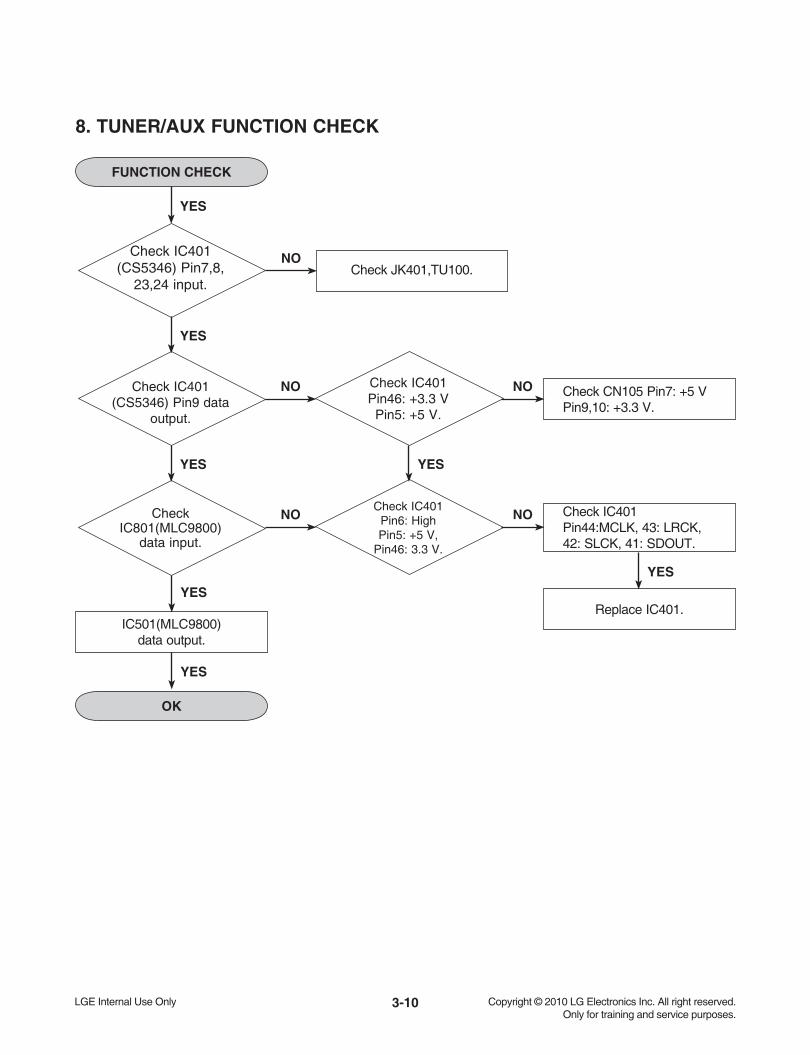
8. TUNER/AUX FUNCTION CHECK
FUNCTION CHECK
Check JK401,TU100.NO
YES
Check IC401(CS5346) Pin7,8,
23,24 input.
YES
YES
Check IC401(CS5346) Pin9 data
output.
YES
Check IC401Pin46: +3.3 V
Pin5: +5 V.
Check CN105 Pin7: +5 VPin9,10: +3.3 V.
NONO
CheckIC801(MLC9800)
data input.
YES
YES
Check IC401Pin6: HighPin5: +5 V,
Pin46: 3.3 V.
Check IC401Pin44:MCLK, 43: LRCK,42: SLCK, 41: SDOUT.
NONO
Replace IC401.IC501(MLC9800)
data output.
OK
YES

3-11
9. TUNER FUNCTION CHECK
TUNER FUNCTION CHECK
Check tuner module voltage(Pin4: +3.3 V).
NOCheck tunermodule(TU100)
operation.
YES
YES
Check IC102 Pin21, 22, 23, 24, 25data in/output. Check tuner module data.
NO
YES
Refer to function check.

3-12
CDP TROUBLESHOOTIHG GUIDE
CD FUNCTION
YES
Can thedisc insert?
NO Is Motor_open/close ok? (IC301 Pin10,11)
NO
Refer to function check.
YES
Disc readingis ok?
Is no signal at spk?
YES
Is Motor ok?(about 12 Ω)
Is load +,- ok?
YES
Check the signal of
IC302 Pin34,35,36.NO
YES
Check the signal (16.0344 MHz)
of IC302 Pin31.
NO
YES
Check IC801input/output and
control line.
NO
YES
YES
Check loading motor.NO
OPU driving (Focus and tracking) is ok?
NOFocus/
tracking/sled signalis ok?
NO Check IC301 (Motor drive IC).
NO
Is the PD(CN301Pin12) about 180mV?
YES
Check Vcc of IC302.
Check Cristal (X301).NO Replace Cristal
(X301).
Replace IC801.
Check IC301.
YES
1. CD FUNCTION
Check OPU(pick-up).
NO

3-13
USB FUNCTION
Check usb_5V. Display “NO USB”.
YES
YES
Check usb_D+/D-(R501,R502).
YES
Plug-in usb device.
Check CN401.NONO
YES
Display “READ”.
YES
Display “NO FILE”.
YES
Check usb jack (JK501).NO
Replace IC801.NO
Check IC801(Pin116, 117).
Check usb audio fi le in usb device (MP3, WMA fi le is playable)
YES
2. USB FUNCTION
3-14
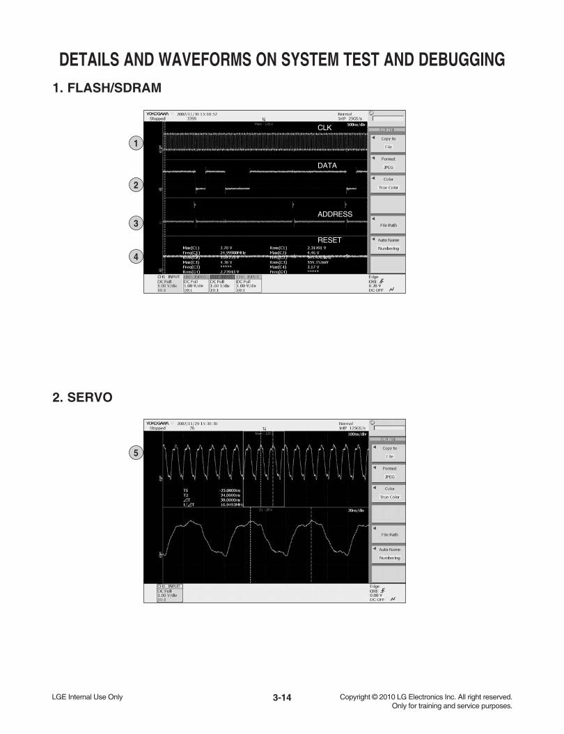
DETAILS AND WAVEFORMS ON SYSTEM TEST AND DEBUGGING1. FLASH/SDRAM
1
2
3
4
CLK
DATA
ADDRESS
RESET
2. SERVO
5

3-15
6
7
8
9
FE
TE
FOD
RF
3. AUDIO PATH
10
11
12
BCK
LRCK
DATA
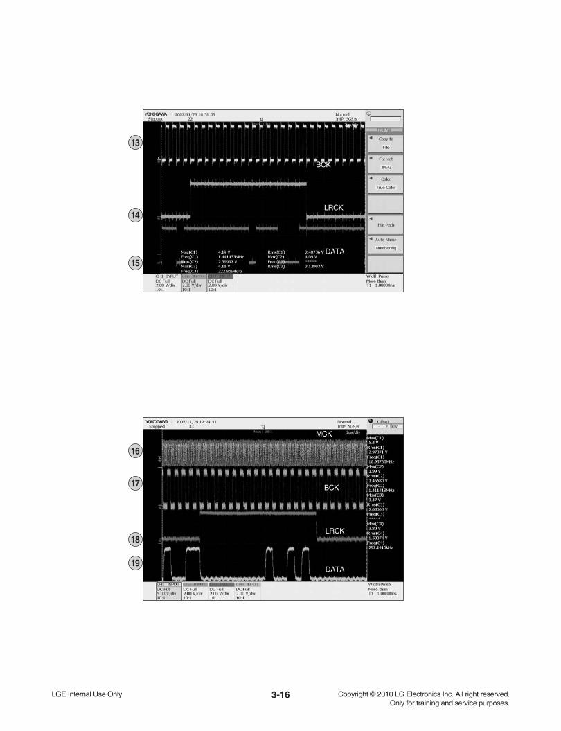
3-16
13
14
15
BCK
LRCK
DATA
16
17
18
MCK
BCK
LRCK
DATA19

3-17
20
21
22
USB_5V
D+
D-
3-18
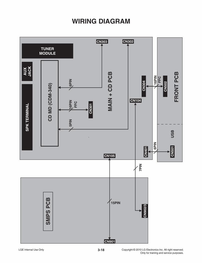
WIRING DIAGRAM
16P
IN5P
IN
SP
K T
ER
MIN
AL
TUNERMODULE
CD
MD
(C
DM
-340
)
MA
IN +
CD
PC
B
16P
IN
US
BF
RO
NT
PC
B
SM
PS
PC
B
6PIN
CN
501
CN
502
CN
304
CN
401
CN
301
FF
C
FF
C
7PIN
AU
XJA
CK
6PIN
15PIN
CN105
CN302CN303
CN901
CN
902/
3
CN104
3-19
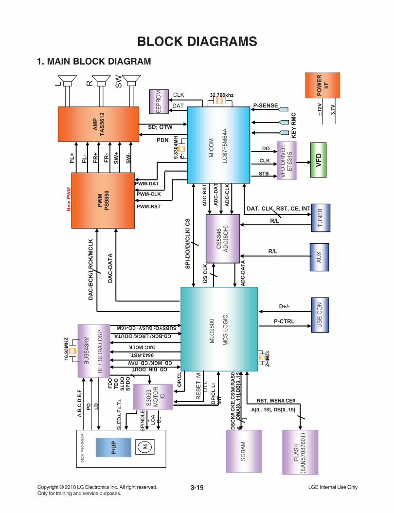
BLOCK DIAGRAMS1. MAIN BLOCK DIAGRAM
P/U
P
M
A,B
,C,D
,E,F
PD LD
CD_DIN_DOUTCD_MCK/CD_R/W
BUSY; CD-16M SUBSYQ;
9543-RST;
VFD
AM
PTA
S561
2
DM
A[0.
.11]
,DB
[0..1
5]
DSC
K#,
CK
E,C
S0#,
RA
S0#
TDO
SLD
OSP
DO
FDO
12MH
Z16.9
3MH
Z
POW
ERI/F
3.7V12
V
DAT, CLK, RST, CE, INT
RST, WEN#,CE#
A[0.. 18], DB[0..15]
OP/
CL
OP/
CL
LI
MIT
CD-BCK/ LRCK/ DOUTA
DAC-MCLK
P-SENSEPW
MPS
9850
DO
STB
CLK
ADC
-CLK
ADC
-DA
T
ADC
-RST
ADC
-DA
TA
R/L
R/L
I2S
CLK
DA
C-B
CK
/LR
CK
/MC
LK
DA
C-D
ATA
PWM-RST
PWM-CLK
PWM-DAT
PDN
SD; OTW
FL+
FL-
FR+
FR-
D+/-
P-CTRL
RL
DAT
CLK
SPI-D
O/D
I/CLK
/ CS
RM
CK
EY
9.83
04M
HZ
32.766khz
New
PW
M
SW
SW+
SW-

3-20
2. SMPS BLOCK DIAGRAM
PVD
D
+¡
Noi
seFi
lter
Blo
ck(X
-cap
Line
Filt
er)
Snub
ber
Blo
ck
Mai
nSM
PS IC
Blo
ck
T R A N S
Snub
ber
Blo
ck
¡ ¡
Phot
o co
uple
r
Phot
o co
uple
r
Phot
o co
uple
r
FL+
FL-
On/
Off
Vkk
On/
Off
5V5V
LD
O
12V
12V
Reg
ulat
ion
Blo
ck
3.7V
A
P.C
TL
On/
Off O
n/O
ff
¡ ¡
¡
¡
¡
¡
¡
¡
AMP
SMPS
ICW
ith F
ETB
lock
¡
F U S E
Y-C
apY-C
ap
¡
T R A N S
SMPS
¡
5.6V
A
CD
P.C
TL
CN
901
CN
902/
3
Feed
back
Feed
back
A
1
2
3
4
5
6
7
8
9
10
11
12
B C D E F G H I J K L M N O P Q R S T
CAUTION: Danger if fuse is incorrectly replaced.
Replace only with the type identical to fuse rating and(or) model name described in main label.
WarningParts that are shaded are critical withrespect to risk of fire or electrical shock.
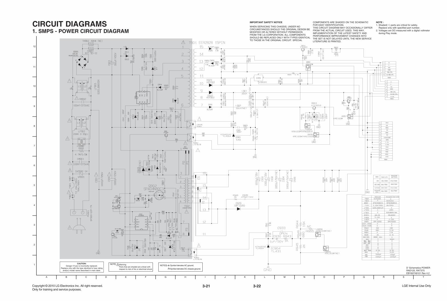
D’ Schemetics POWERRAD125, RAT375EBY60749101 Rev 4.2
IMPORTANT SAFETY NOTICE
WHEN SERVICING THIS CHASSIS, UNDER NO CIRCUMSTANCES SHOULD THE ORIGINAL DESIGN BEMODIFIED OR ALTERED WITHOUT PERMISSIONFROM THE LG CORPORATION. ALL COMPONENTSSHOULD BE REPLACED ONLY WITH TYPES IDENTICAL TO THOSE IN THE ORIGINAL CIRCUIT. SPECIAL
COMPONENTS ARE SHADED ON THE SCHEMATICFOR EASY IDENTIFICATION.THIS CIRCUIT DIAGRAM MAY OCCASIONALLY DIFFER FROM THE ACTUAL CIRCUIT USED. THIS WAY,IMPLEMENTATION OF THE LATEST SAFETY ANDPERFORMANCE IMPROVEMENT CHANGES INTOTHE SET IS NOT DELAYED UNTIL THE NEW SERVICELITERATURE IS PRINTED.
NOTE :1. Shaded( ) parts are critical for safety.
Replace only with specified part number.2. Voltages are DC-measured with a digital voltmeter
during Play mode.
CIRCUIT DIAGRAMS1. SMPS - POWER CIRCUIT DIAGRAM
3-21 3-22
A
1
2
3
4
5
6
7
8
9
10
11
12
B C D E F G H I J K L M N O P Q R S T
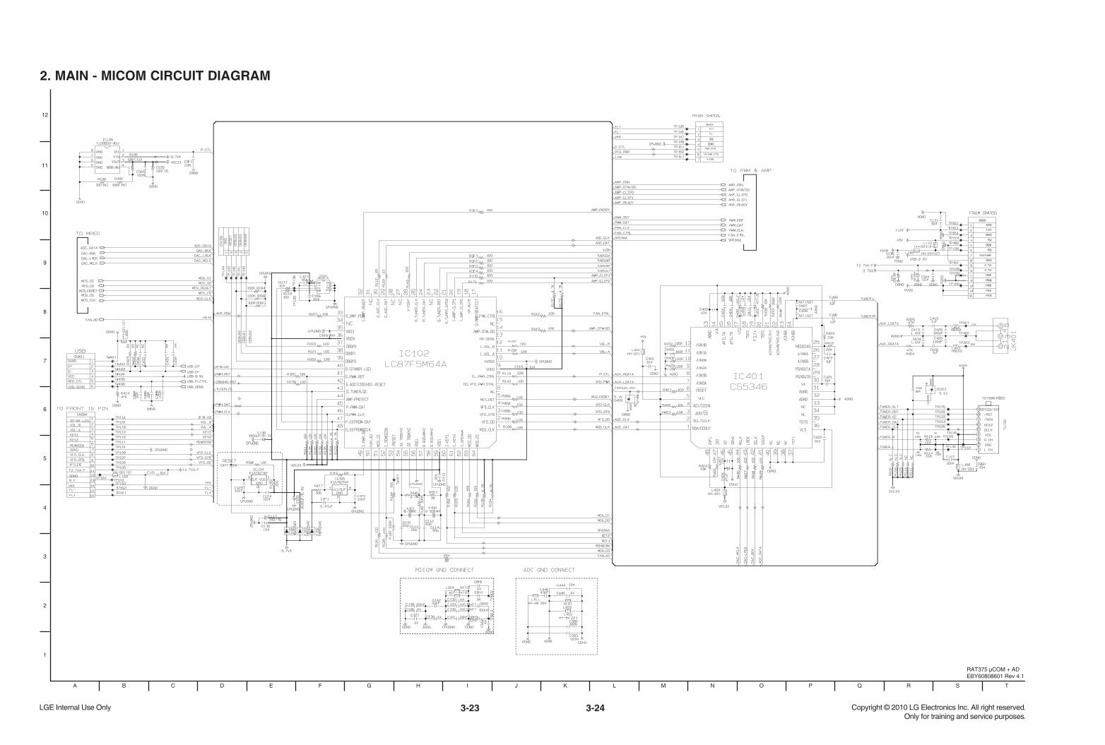
RAT375 µCOM + ADEBY60808601 Rev 4.1
2. MAIN - MICOM CIRCUIT DIAGRAM
3-23 3-24

A
1
2
3
4
5
6
7
8
9
10
11
12
B C D E F G H I J K L M N O P Q R S T
RAT375 CD DSP + SERVOEBY60808601 Rev 4.1
3. MAIN - CD DSP & SERVO CIRCUIT DIAGRAM
3-25 3-26
A
1
2
3
4
5
6
7
8
9
10
11
12
B C D E F G H I J K L M N O P Q R S T
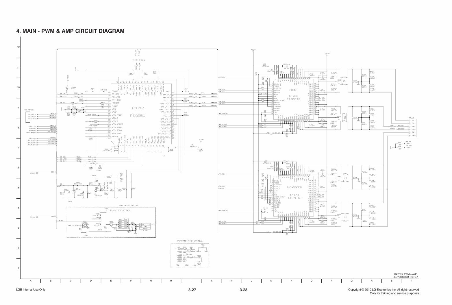
RAT375 PWM + AMPEBY60808601 Rev 4.1
3-27 3-28
4. MAIN - PWM & AMP CIRCUIT DIAGRAM
A
1
2
3
4
5
6
7
8
9
10
11
12
B C D E F G H I J K L M N O P Q R S T
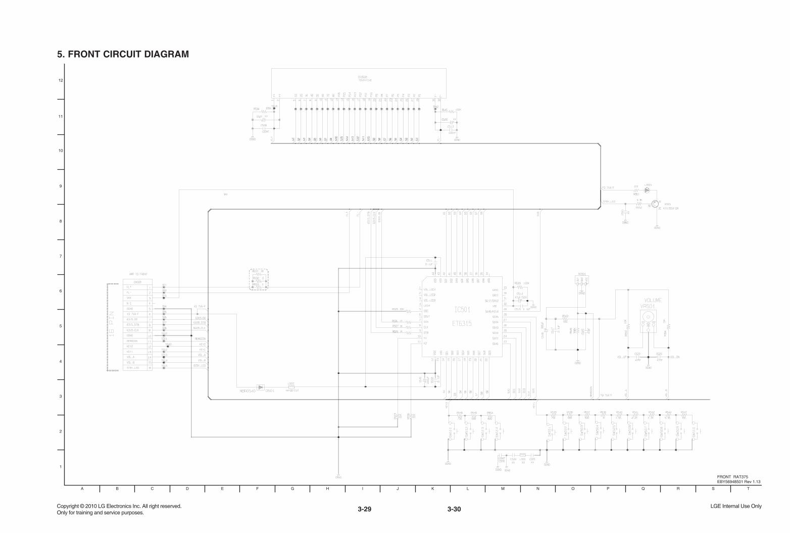
FRONT RAT375 EBY56948501 Rev 1.13
5. FRONT CIRCUIT DIAGRAM
3-29 3-30
A
1
2
3
4
5
6
7
8
9
10
11
12
B C D E F G H I J K L M N O P Q R S T
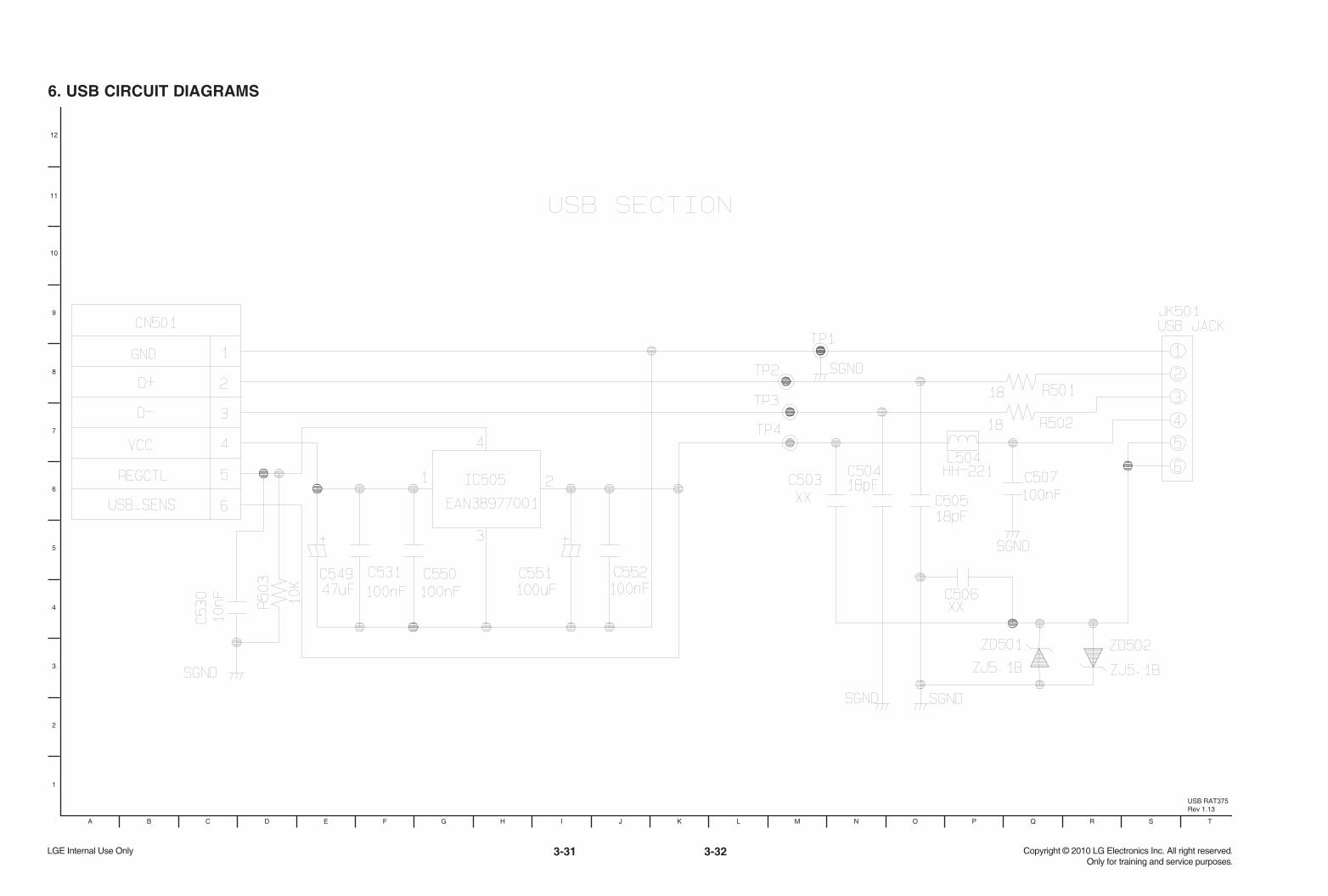
USB RAT375Rev 1.13
6. USB CIRCUIT DIAGRAMS
3-31 3-32
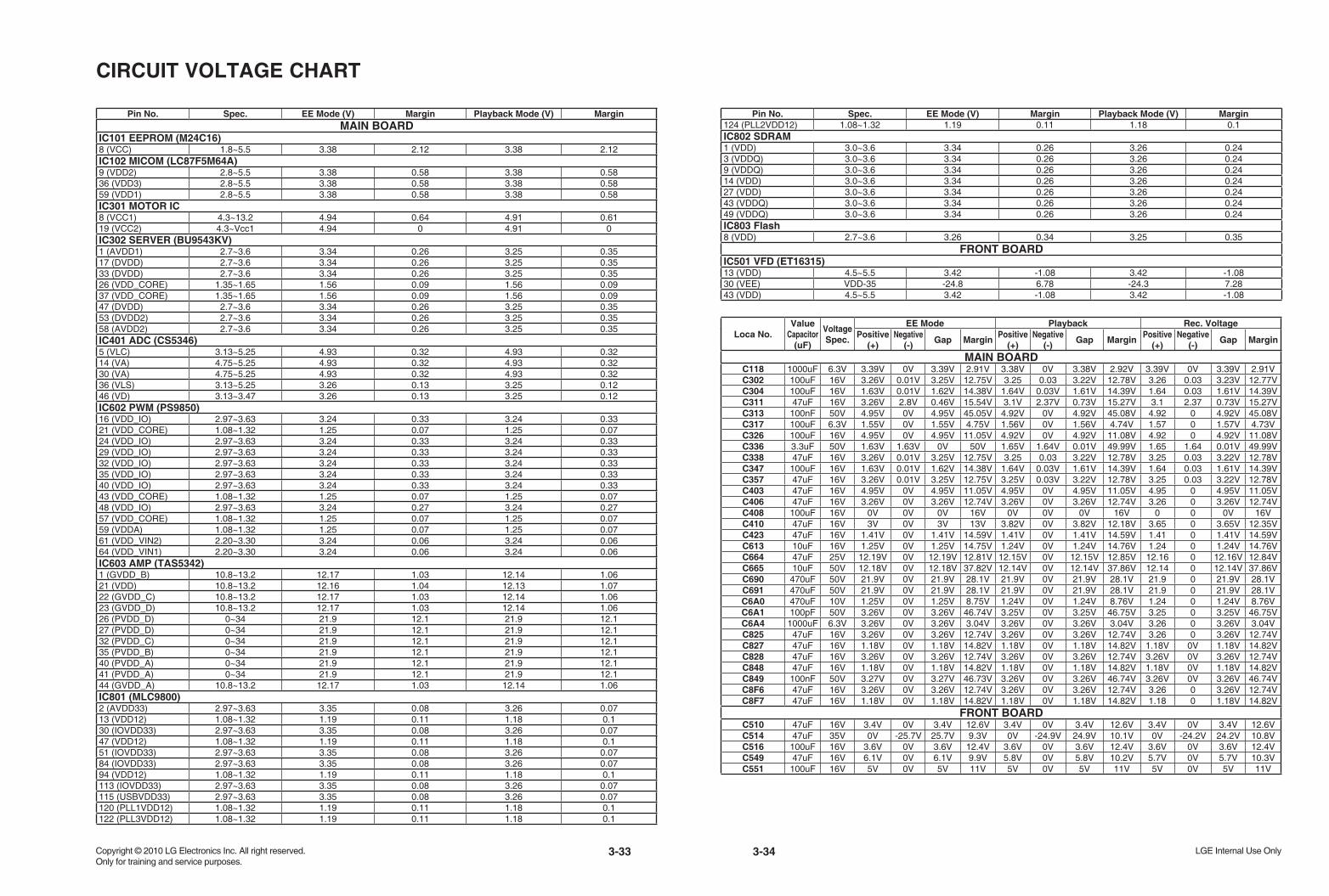
CIRCUIT VOLTAGE CHART
3-33 3-34
Pin No. Spec. EE Mode (V) Margin Playback Mode (V) MarginMAIN BOARD
IC101 EEPROM (M24C16)8 (VCC) 1.8~5.5 3.38 2.12 3.38 2.12IC102 MICOM (LC87F5M64A)9 (VDD2) 2.8~5.5 3.38 0.58 3.38 0.5836 (VDD3) 2.8~5.5 3.38 0.58 3.38 0.5859 (VDD1) 2.8~5.5 3.38 0.58 3.38 0.58IC301 MOTOR IC8 (VCC1) 4.3~13.2 4.94 0.64 4.91 0.6119 (VCC2) 4.3~Vcc1 4.94 0 4.91 0IC302 SERVER (BU9543KV)1 (AVDD1) 2.7~3.6 3.34 0.26 3.25 0.3517 (DVDD) 2.7~3.6 3.34 0.26 3.25 0.3533 (DVDD) 2.7~3.6 3.34 0.26 3.25 0.3526 (VDD_CORE) 1.35~1.65 1.56 0.09 1.56 0.0937 (VDD_CORE) 1.35~1.65 1.56 0.09 1.56 0.0947 (DVDD) 2.7~3.6 3.34 0.26 3.25 0.3553 (DVDD2) 2.7~3.6 3.34 0.26 3.25 0.3558 (AVDD2) 2.7~3.6 3.34 0.26 3.25 0.35IC401 ADC (CS5346)5 (VLC) 3.13~5.25 4.93 0.32 4.93 0.3214 (VA) 4.75~5.25 4.93 0.32 4.93 0.3230 (VA) 4.75~5.25 4.93 0.32 4.93 0.3236 (VLS) 3.13~5.25 3.26 0.13 3.25 0.1246 (VD) 3.13~3.47 3.26 0.13 3.25 0.12IC602 PWM (PS9850)16 (VDD_IO) 2.97~3.63 3.24 0.33 3.24 0.3321 (VDD_CORE) 1.08~1.32 1.25 0.07 1.25 0.0724 (VDD_IO) 2.97~3.63 3.24 0.33 3.24 0.3329 (VDD_IO) 2.97~3.63 3.24 0.33 3.24 0.3332 (VDD_IO) 2.97~3.63 3.24 0.33 3.24 0.3335 (VDD_IO) 2.97~3.63 3.24 0.33 3.24 0.3340 (VDD_IO) 2.97~3.63 3.24 0.33 3.24 0.3343 (VDD_CORE) 1.08~1.32 1.25 0.07 1.25 0.0748 (VDD_IO) 2.97~3.63 3.24 0.27 3.24 0.2757 (VDD_CORE) 1.08~1.32 1.25 0.07 1.25 0.0759 (VDDA) 1.08~1.32 1.25 0.07 1.25 0.0761 (VDD_VIN2) 2.20~3.30 3.24 0.06 3.24 0.0664 (VDD_VIN1) 2.20~3.30 3.24 0.06 3.24 0.06IC603 AMP (TAS5342)1 (GVDD_B) 10.8~13.2 12.17 1.03 12.14 1.0621 (VDD) 10.8~13.2 12.16 1.04 12.13 1.0722 (GVDD_C) 10.8~13.2 12.17 1.03 12.14 1.0623 (GVDD_D) 10.8~13.2 12.17 1.03 12.14 1.0626 (PVDD_D) 0~34 21.9 12.1 21.9 12.127 (PVDD_D) 0~34 21.9 12.1 21.9 12.132 (PVDD_C) 0~34 21.9 12.1 21.9 12.135 (PVDD_B) 0~34 21.9 12.1 21.9 12.140 (PVDD_A) 0~34 21.9 12.1 21.9 12.141 (PVDD_A) 0~34 21.9 12.1 21.9 12.144 (GVDD_A) 10.8~13.2 12.17 1.03 12.14 1.06IC801 (MLC9800)2 (AVDD33) 2.97~3.63 3.35 0.08 3.26 0.0713 (VDD12) 1.08~1.32 1.19 0.11 1.18 0.130 (IOVDD33) 2.97~3.63 3.35 0.08 3.26 0.0747 (VDD12) 1.08~1.32 1.19 0.11 1.18 0.151 (IOVDD33) 2.97~3.63 3.35 0.08 3.26 0.0784 (IOVDD33) 2.97~3.63 3.35 0.08 3.26 0.0794 (VDD12) 1.08~1.32 1.19 0.11 1.18 0.1113 (IOVDD33) 2.97~3.63 3.35 0.08 3.26 0.07115 (USBVDD33) 2.97~3.63 3.35 0.08 3.26 0.07120 (PLL1VDD12) 1.08~1.32 1.19 0.11 1.18 0.1122 (PLL3VDD12) 1.08~1.32 1.19 0.11 1.18 0.1
Pin No. Spec. EE Mode (V) Margin Playback Mode (V) Margin124 (PLL2VDD12) 1.08~1.32 1.19 0.11 1.18 0.1IC802 SDRAM1 (VDD) 3.0~3.6 3.34 0.26 3.26 0.243 (VDDQ) 3.0~3.6 3.34 0.26 3.26 0.249 (VDDQ) 3.0~3.6 3.34 0.26 3.26 0.2414 (VDD) 3.0~3.6 3.34 0.26 3.26 0.2427 (VDD) 3.0~3.6 3.34 0.26 3.26 0.2443 (VDDQ) 3.0~3.6 3.34 0.26 3.26 0.2449 (VDDQ) 3.0~3.6 3.34 0.26 3.26 0.24IC803 Flash8 (VDD) 2.7~3.6 3.26 0.34 3.25 0.35
FRONT BOARDIC501 VFD (ET16315)13 (VDD) 4.5~5.5 3.42 -1.08 3.42 -1.0830 (VEE) VDD-35 -24.8 6.78 -24.3 7.2843 (VDD) 4.5~5.5 3.42 -1.08 3.42 -1.08
Loca No.Value
Capacitor (uF)
Voltage Spec.
EE Mode Playback Rec. VoltagePositive
(+)Negative
(-)Gap Margin
Positive (+)
Negative (-)
Gap MarginPositive
(+)Negative
(-)Gap Margin
MAIN BOARDC118 1000uF 6.3V 3.39V 0V 3.39V 2.91V 3.38V 0V 3.38V 2.92V 3.39V 0V 3.39V 2.91VC302 100uF 16V 3.26V 0.01V 3.25V 12.75V 3.25 0.03 3.22V 12.78V 3.26 0.03 3.23V 12.77VC304 100uF 16V 1.63V 0.01V 1.62V 14.38V 1.64V 0.03V 1.61V 14.39V 1.64 0.03 1.61V 14.39VC311 47uF 16V 3.26V 2.8V 0.46V 15.54V 3.1V 2.37V 0.73V 15.27V 3.1 2.37 0.73V 15.27VC313 100nF 50V 4.95V 0V 4.95V 45.05V 4.92V 0V 4.92V 45.08V 4.92 0 4.92V 45.08VC317 100uF 6.3V 1.55V 0V 1.55V 4.75V 1.56V 0V 1.56V 4.74V 1.57 0 1.57V 4.73VC326 100uF 16V 4.95V 0V 4.95V 11.05V 4.92V 0V 4.92V 11.08V 4.92 0 4.92V 11.08VC336 3.3uF 50V 1.63V 1.63V 0V 50V 1.65V 1.64V 0.01V 49.99V 1.65 1.64 0.01V 49.99VC338 47uF 16V 3.26V 0.01V 3.25V 12.75V 3.25 0.03 3.22V 12.78V 3.25 0.03 3.22V 12.78VC347 100uF 16V 1.63V 0.01V 1.62V 14.38V 1.64V 0.03V 1.61V 14.39V 1.64 0.03 1.61V 14.39VC357 47uF 16V 3.26V 0.01V 3.25V 12.75V 3.25V 0.03V 3.22V 12.78V 3.25 0.03 3.22V 12.78VC403 47uF 16V 4.95V 0V 4.95V 11.05V 4.95V 0V 4.95V 11.05V 4.95 0 4.95V 11.05VC406 47uF 16V 3.26V 0V 3.26V 12.74V 3.26V 0V 3.26V 12.74V 3.26 0 3.26V 12.74VC408 100uF 16V 0V 0V 0V 16V 0V 0V 0V 16V 0 0 0V 16VC410 47uF 16V 3V 0V 3V 13V 3.82V 0V 3.82V 12.18V 3.65 0 3.65V 12.35VC423 47uF 16V 1.41V 0V 1.41V 14.59V 1.41V 0V 1.41V 14.59V 1.41 0 1.41V 14.59VC613 10uF 16V 1.25V 0V 1.25V 14.75V 1.24V 0V 1.24V 14.76V 1.24 0 1.24V 14.76VC664 47uF 25V 12.19V 0V 12.19V 12.81V 12.15V 0V 12.15V 12.85V 12.16 0 12.16V 12.84VC665 10uF 50V 12.18V 0V 12.18V 37.82V 12.14V 0V 12.14V 37.86V 12.14 0 12.14V 37.86VC690 470uF 50V 21.9V 0V 21.9V 28.1V 21.9V 0V 21.9V 28.1V 21.9 0 21.9V 28.1VC691 470uF 50V 21.9V 0V 21.9V 28.1V 21.9V 0V 21.9V 28.1V 21.9 0 21.9V 28.1VC6A0 470uF 10V 1.25V 0V 1.25V 8.75V 1.24V 0V 1.24V 8.76V 1.24 0 1.24V 8.76VC6A1 100pF 50V 3.26V 0V 3.26V 46.74V 3.25V 0V 3.25V 46.75V 3.25 0 3.25V 46.75VC6A4 1000uF 6.3V 3.26V 0V 3.26V 3.04V 3.26V 0V 3.26V 3.04V 3.26 0 3.26V 3.04VC825 47uF 16V 3.26V 0V 3.26V 12.74V 3.26V 0V 3.26V 12.74V 3.26 0 3.26V 12.74VC827 47uF 16V 1.18V 0V 1.18V 14.82V 1.18V 0V 1.18V 14.82V 1.18V 0V 1.18V 14.82VC828 47uF 16V 3.26V 0V 3.26V 12.74V 3.26V 0V 3.26V 12.74V 3.26V 0V 3.26V 12.74VC848 47uF 16V 1.18V 0V 1.18V 14.82V 1.18V 0V 1.18V 14.82V 1.18V 0V 1.18V 14.82VC849 100nF 50V 3.27V 0V 3.27V 46.73V 3.26V 0V 3.26V 46.74V 3.26V 0V 3.26V 46.74VC8F6 47uF 16V 3.26V 0V 3.26V 12.74V 3.26V 0V 3.26V 12.74V 3.26 0 3.26V 12.74VC8F7 47uF 16V 1.18V 0V 1.18V 14.82V 1.18V 0V 1.18V 14.82V 1.18 0 1.18V 14.82V
FRONT BOARDC510 47uF 16V 3.4V 0V 3.4V 12.6V 3.4V 0V 3.4V 12.6V 3.4V 0V 3.4V 12.6VC514 47uF 35V 0V -25.7V 25.7V 9.3V 0V -24.9V 24.9V 10.1V 0V -24.2V 24.2V 10.8VC516 100uF 16V 3.6V 0V 3.6V 12.4V 3.6V 0V 3.6V 12.4V 3.6V 0V 3.6V 12.4VC549 47uF 16V 6.1V 0V 6.1V 9.9V 5.8V 0V 5.8V 10.2V 5.7V 0V 5.7V 10.3VC551 100uF 16V 5V 0V 5V 11V 5V 0V 5V 11V 5V 0V 5V 11V

PRINTED CIRCUIT BOARD DIARGAMS1. MAIN P.C. BOARD DIAGRAM ( TOP VIEW )
3-35 3-36
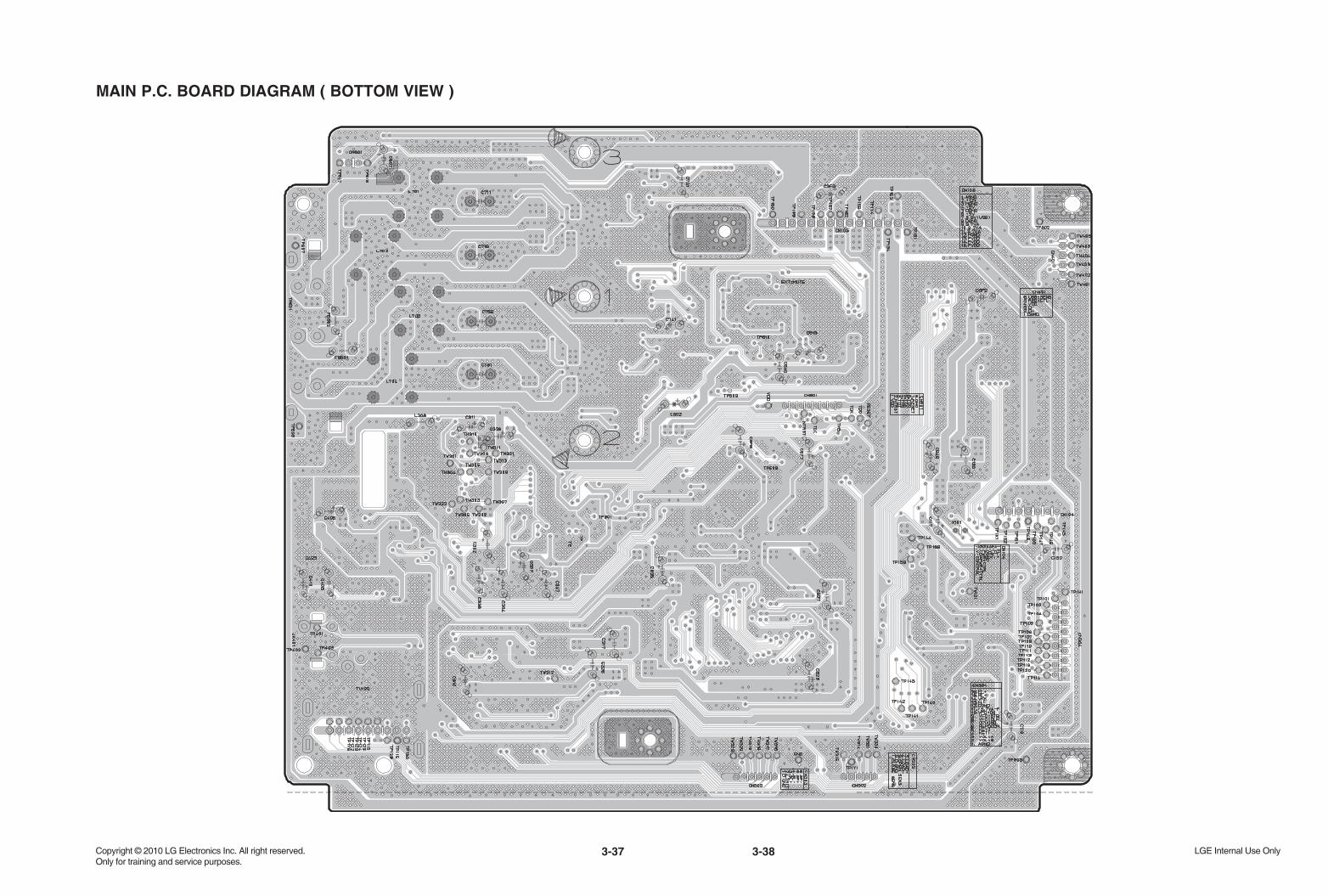
MAIN P.C. BOARD DIAGRAM ( BOTTOM VIEW )
3-37 3-38

2. SMPS P.C. BOARD DIAGRAM
3-39 3-40
WarningParts that are shaded are critical withrespect to risk of fire or electrical shock.
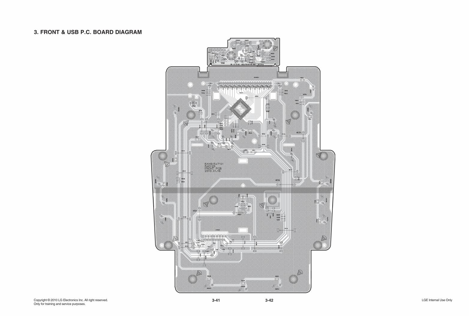
3. FRONT & USB P.C. BOARD DIAGRAM
3-41 3-42

3-43 3-44
MEMO MEMO