8/13/2019 Lec 05 WFig Ver 01
http://slidepdf.com/reader/full/lec-05-wfig-ver-01 1/16
Common Emitter Amplifier Frequency Response
Objectives
To analyze the CE amplifiers and to calculate different poles and zeros which
determine its frequency response
To calculate the dominant poles and the CE amplifier bandwidth To analyze the effect of the emitter resistor on the CE amplifier gain and
bandwidth
Introduction
In the last lecture the frequency response of the amplifier circuits were examined
!lso" the frequency response of the common source amplifier was calculated and the
dominant poles were determined In this lecture the frequency response of the
common emitter amplifier will be considered using the #CTC and OCTC techniques
introduced in the last lecture The design trade$off using the emitter resistor will be
explored
Short-Circuit Time Constant Method to Determine ω L
% !s mentioned in the last lecture midband gain and upper and lower cutoff
frequencies that define bandwidth of the amplifier are of more interest than
complete transfer function
% In the next example the low cutoff frequency of the CE amplifier will be
determined using the #CTC method
Example &' (erive an expression for the low cutoff frequency for the CE amplifier
circuit in )igure & using the #CTC method
)ig$& in *+ec,-.,/er,-&vsd0Figure Common Emitter Amplifier Circuit
8/13/2019 Lec 05 WFig Ver 01
http://slidepdf.com/reader/full/lec-05-wfig-ver-01 2/16
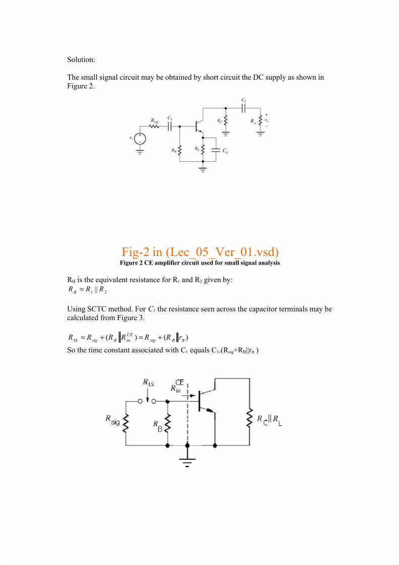
#olution'
The small signal circuit may be obtained by short circuit the (C supply as shown in
)igure 1
)ig$1 in *+ec,-.,/er,-&vsd0Figure ! CE amplifier circuit used for small signal analysis
2 3 is the equivalent resistance for 2 & and 2 1 given by'
& 144 B R R R=
5sing #CTC method )or C 1 the resistance seen across the capacitor terminals may be
calculated from )igure 6
& * 0 * 0CE
S sig B in sig B R R R R R R r π = + = +
#o the time constant associated with C& equals C&*2 sig72 344r π 0

8/13/2019 Lec 05 WFig Ver 01
http://slidepdf.com/reader/full/lec-05-wfig-ver-01 3/16
)ig$6 in *+ec,-.,/er,-&vsd0Figure " Circuit used to calculate the short-circuit time constant associated #ith C 1
)or C 2 the resistance seen across the capacitor terminals may be calculated from
)igure 8
1 * 0 * 0CE
S L C out L C o
L C
R R R R R R r
R R
= + = +
≅ +#o the time constant associated with C1 equals C1*2 +72 C0
)ig$9 in *+ec,-.,/er,-&vsd0Figure $ Circuit used to calculate the short-circuit time constant associated #ith C 2
)or C E the resistance seen across the capacitor terminals may be calculated from
)igure :

8/13/2019 Lec 05 WFig Ver 01
http://slidepdf.com/reader/full/lec-05-wfig-ver-01 4/16
* 0
&
sig BCC out ES E E
o
r R R R R R R
π
β
+= =
+
#o the time constant associated with CE equals CE2 E#
)ig$. in *+ec,-.,/er,-&vsd0Figure % Circuit used to calculate the short-circuit time constant associated #ith C E
The low cutoff frequency is calculated using the #CTC as'6
&& 1
& & & &
* * 00 * 0 * 0
&
Li
iS i sig B L C sig B
E E
o
R C C R R r C R R r R RC R
π π
ω
β
=≅ = + +∑
+ + + ÷ ÷+
;lease note that due to the finite input resistance of the CE amplifier compared to the
C# amplifier" the lower cutoff frequency will be higher in the CE amplifier compared
to the C# amplifier
Example 1' Calculate the low cutoff frequency for the common emitter amplifier in
)igure & using the #CTC method !ssume' /CC<&1/" 2 sig<&= Ω" 2 &<&-= Ω" 2 1<6-= Ω"
2 C<96= Ω" 2 E<&6= Ω" 2 +<&--= Ω" C&<1µ)" C1< -&µ)" and CE<.-µ)
#olution'
2efer to Example & solution
8/13/2019 Lec 05 WFig Ver 01
http://slidepdf.com/reader/full/lec-05-wfig-ver-01 5/16
& 1
& & &
* * 00 * 0 * 0
&
L
sig B L C sig B
E E
o
C R R r C R R r R RC R
π π
ω
β
≅ + ++ + +
÷ ÷+
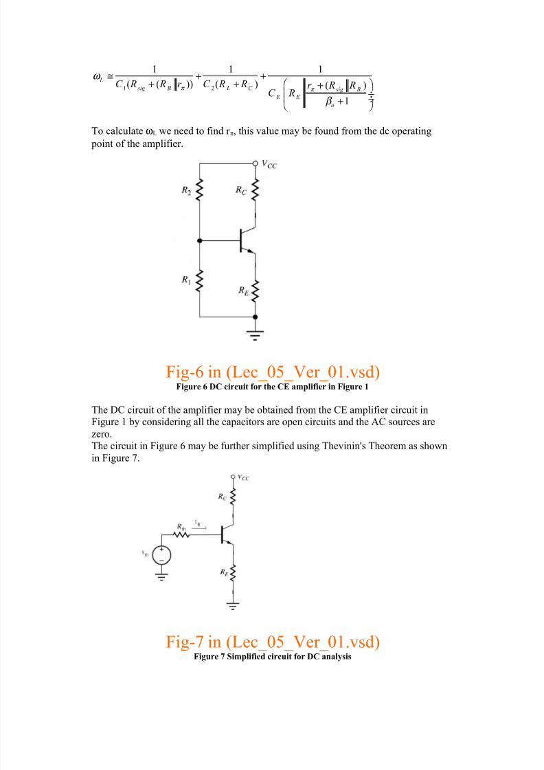
To calculate ω+ we need to find r π" this value may be found from the dc operating point of the amplifier
)ig$8 in *+ec,-.,/er,-&vsd0Figure & DC circuit for the CE amplifier in Figure
The (C circuit of the amplifier may be obtained from the CE amplifier circuit in
)igure & by considering all the capacitors are open circuits and the !C sources are
zero
The circuit in )igure 8 may be further simplified using Thevinin>s Theorem as shown
in )igure :
)ig$: in *+ec,-.,/er,-&vsd0Figure ' Simplified circuit for DC analysis
8/13/2019 Lec 05 WFig Ver 01
http://slidepdf.com/reader/full/lec-05-wfig-ver-01 6/16
& 144 :.th B R R R R k = = = Ω
&
& 1
&- &1 6
9-th CC
RV V V
R R= = =
+
!pplying ?/+ in the 3$E loop and assuming that the transistor is in the active mode'
* *& 0 0
6 -:&88
* *& 0 0 :. &-&@&6
th B th BE E E
BE B th o E
th BE B
th o E
V I R V I R
V I R R
V V I A
R R
β
µ β
∴ = + += + + +
− −∴ = = =
+ + +&88C o B E I I I mAβ = ≅ =
!pplying ?/+ at the C$E loop
&1 &88@*&6 960 1:CC C C CE E E
CE
V I R V I R
V V ∴ = + +∴ = − + =#ince /CE A /CEsat " then the transistor is in active region as assumed
B$point < *&88m!" 1:/0
1.&.
&88
T
B
V mV r k
I Aπ
µ = = = Ω
#ubstitute in the expression of ω+
111 8 :.- &-8D sec L rad ω ≅ + + =
Direct Determination of (igh-Frequency )oles and *eros+
#imilar to what we did in the last lecture The high frequency poles and zeros may be
determined by direct analysis In this case all the coupling and bypass capacitors may
be considered short circuit Fowever" the high frequency model of the transistor
should be used since the transistor internal capacitances can>t considered open circuit
at high frequencies The following example will illustrate this method for the common
emitter amplifier
Example 6' (rive an expression for the high frequency response !vF*s0 of the
common emitter amplifier shown in )igure & Fence" determine the midband gain
!mid" high frequency poles and zeros" and the high cutoff frequency
#olution'
The CE amplifier is redrawn for small signal analysis as shown in )igure D by
replacing the transistor in )igure 1 by its high frequency small signal model
!ll the coupling and bypass capacitors are considered short circuit at high frequency
The biasing resistors 2 & and 2 1 are combined into 2 3 & 144 B R R R∴ =

8/13/2019 Lec 05 WFig Ver 01
http://slidepdf.com/reader/full/lec-05-wfig-ver-01 7/16
)ig$D in *+ec,-.,/er,-&vsd0Figure , The CE amplifier in Figure ! redra#n #ith the transistor replaced y its high frequency
small signal model
The small$signal model can be simplified by using Thevinin>s theorem as shown in
)igure The simplified circuit is shown in )igure &-
)ig$ in *+ec,-.,/er,-&vsd0Figure . /sing The0inin1s Theorem to simplify the CE amplifier circuit in Figure ,
8/13/2019 Lec 05 WFig Ver 01
http://slidepdf.com/reader/full/lec-05-wfig-ver-01 8/16
Bth sig
sig B
Rv v
R R=
+ and sig B
th
sig B
R R R
R R=
+
1
thth
th x
v r v
R r r
π
π
=+ + and 1 * 0th th xr r R r π = +
!lso" 44 44 L L C o R R R r ′ =
)ig$&- in *+ec,-.,/er,-&vsd0Figure 2 Simplified circuit to calculate the frequency response of the CE amplifier
Griting the two nodal equations at nodes ! and 3 in the frequency domain"
1
1
* 0 -
* 0 -
be thbe be o
th
om gs o be
L
v vv sC v v sC
R
v g v v v sC
R
π µ
µ
′ −′ ′+ + − =
′+ + − =′
#olving the last two equations by eliminating vH be yields"
8/13/2019 Lec 05 WFig Ver 01
http://slidepdf.com/reader/full/lec-05-wfig-ver-01 9/16
( )
th1o
1
1
1 1
1
1
1
* $ 0*s0*s0
& & &
* $ 0* 0* 0
* 0 * 0* 0
+et us define &
&
mv
th
m
L th L L th
mo BvH
sig th x sig B
LT m L
th
T
L L th
sC g v
R
C s C C s C g
R R R R R
sC g v s R A s
v s R r R R
RC C C g R
R
sC s C C
R R R
µ
π π µ µ
µ
π µ
π µ
=∆
∆ = + + + + + ÷ ÷ ÷′ ′ ′
∴ = =
+ + ∆
′′= + + + ÷
∴∆ = + +′ ′
1
1
* $ 0* 0
&* 0* 0
m BvH
T th x sig B
L L th
sC g R A s
sC R r R R C C s R C C R R C C
µ
π µ
π µ π µ
∴ =+ +
+ +′ ′
!mid may be found from the last expression by assuming s -
1$ $
* 0* 0 * 0* 0
$
* 0* 0
m L B th m L Bmid
th x sig B th x sig B
o L B
th x sig B
g R R R g R R r A
R r R R r R r R R
R R
r R r R R
π
π
π
β
′ ′∴ = =
+ + + + +
′=
+ + +Figh$frequency response is given by 1 poles" one finite zero and one zero at infinity
)inite right$half plane zero" ω Z < 7 g mC µ A ω T can easily be neglected
)or a polynomial s17 sA&7 A- with roots a and b" if one root is much larger than the
other one" we can assume that a < A& and b< A- A&
-&
& 1
1
1
1
&
!ssume that the midband gain is very large * ie & "and 0
& &&
th T
Lm L m L
th
m m
m th m L
A
A R C
R g R g R C C
R
g g
C g R g R C
µ π
π π
ω
ω
∴ = ≅
′′ ′+ ÷
∴ ≅ + + ≅ ÷′
? ?
#mallest root that gives first pole limits frequency response and determines ω H
#econd pole is important in frequency compensation as it can degrade phase margin
of feedbac= amplifiers
p& p1 p&
&
1
!ssuming * is the dominanat pole0
& H
th T R C
ω ω ω
ω ω ∴ ≅ =
=
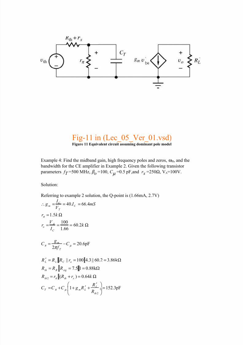
(ominant pole model at high frequencies for C# amplifier is shown in )igure &&
8/13/2019 Lec 05 WFig Ver 01
http://slidepdf.com/reader/full/lec-05-wfig-ver-01 10/16
)ig$&& in *+ec,-.,/er,-&vsd0Figure Equi0alent circuit assuming dominant pole model
Example 9' )ind the midband gain" high frequency poles and zeros" ωF" and the
bandwidth for the CE amplifier in Example 1 iven the following transistor
parameters ! T <.-- JFz" β o <&--" C µ <-. p)"and r x <1.-Ω, /!<&--/.
#olution'
2eferring to example 1 solution" the B$point is *&88m!" 1:/0
9- 889
&.
&--8-1
&88
C m C
T
Ao
C
I g I mS
V
r k
V r k
I
π
∴ = = =
= Ω
= = = Ω
1-8p)1
m
T
g C C
! π µ
π = − =
44 &-- 96 44 8-1 6D8=K L L C o R R R r ′ = = =
:. & -DD=Kth B sig R R R= = =
1 * 0 -89th th x R r R r k π = + = Ω
1& &.16p)
L
T m Lth
R
C C C g R Rπ µ
′
′= + + + = ÷
8/13/2019 Lec 05 WFig Ver 01
http://slidepdf.com/reader/full/lec-05-wfig-ver-01 11/16
&
1
&&-18J radsec
th T R C ω = =
1
1
& && 66& radsecm
m th m L
g
C g R g Rπ
ω
≅ + + ≅ ÷′
&61D radsec g
m # C
ω
µ
= =
It is clear that ω p& is much lower than ω p1 and ωz which means that ω p& is the dominant
pole
&&-18J radEsec
&861
H
H H $H#
ω ω
ω
π
∴ ≅ =
= =
&86 &:- &86 H L B % ! ! $H# H# $H# = − = − ≅
$ &1. //
* 0* 0
o L B
th x sig B
R R A
mid r R r R Rπ
β ′= = −
+ + +
3ain-4and#idth )roduct 5imitations of the C-E Amplifier
!s we can see from the expressions of the midband gain and the CE amplifier
bandwidth 2 th is appearing in both expressions
If Rth is reduced to zero in order to increase the bandwidth" then Rth2 would not be zero
but would be limited to approximately r x
&3G
1
o Lv H
th x
R A
R r r R C th T π
β ω
′ ÷= ≤ ÷ ÷+ +
If Rth < -" r x LLr π so that r x < Rth2 and * 0T m LC C g R µ ′=
&
I3G xr C µ ∴ ≤
If we used the same values in Example 9
I3G DI radEsec∴ ≤
The !ctual 3G in Example 9 is &669 radsec
6pen-Circuit Time Constant Method to Determine ω H
% !s mentioned in the last lecture the open$circuit time constants associated
with the transistor capacitances may be used to simplify the determination of
the high cutoff frequency of the amplifier
% In the next example the high cutoff frequency of the CE amplifier will bedetermined using the OCTC method
8/13/2019 Lec 05 WFig Ver 01
http://slidepdf.com/reader/full/lec-05-wfig-ver-01 12/16
Example .' (erive an expression for the high cutoff frequency for the circuit in
Example 9 using the OCTC method
#olution'
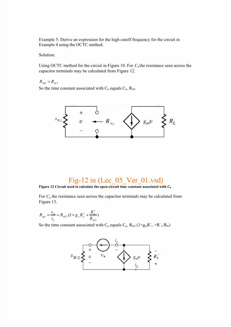
5sing OCTC method for the circuit in )igure &- )or C π the resistance seen across the
capacitor terminals may be calculated from )igure &1
1& th R Rπ =#o the time constant associated with Cπ equals Cπ 2 th1
)ig$&1 in *+ec,-.,/er,-&vsd0Figure ! Circuit used to calculate the open-circuit time constant associated #ith C
)or C µ the resistance seen across the capacitor terminals may be calculated from
)igure &6
x1
x 1
v*& 0
i
m
Lo th L
th
R R R g R
R
µ
′′= = + +
#o the time constant associated with Cµ equals Cµ 2 th1 *&7gm2H+ 72H+2 th0
8/13/2019 Lec 05 WFig Ver 01
http://slidepdf.com/reader/full/lec-05-wfig-ver-01 13/16
)ig$&6 in *+ec,-.,/er,-&vsd0Figure " Circuit used to calculate the open-circuit time constant associated #ith C
The high cutoff frequency is calculated using the OCTC as'
1
&
& & &
1 H
io ii
R C R C r C R C o o th T
ω
π π µ µ =
≅ = =+∑
Ghich is the same expression found before using direct calculations in Example 6
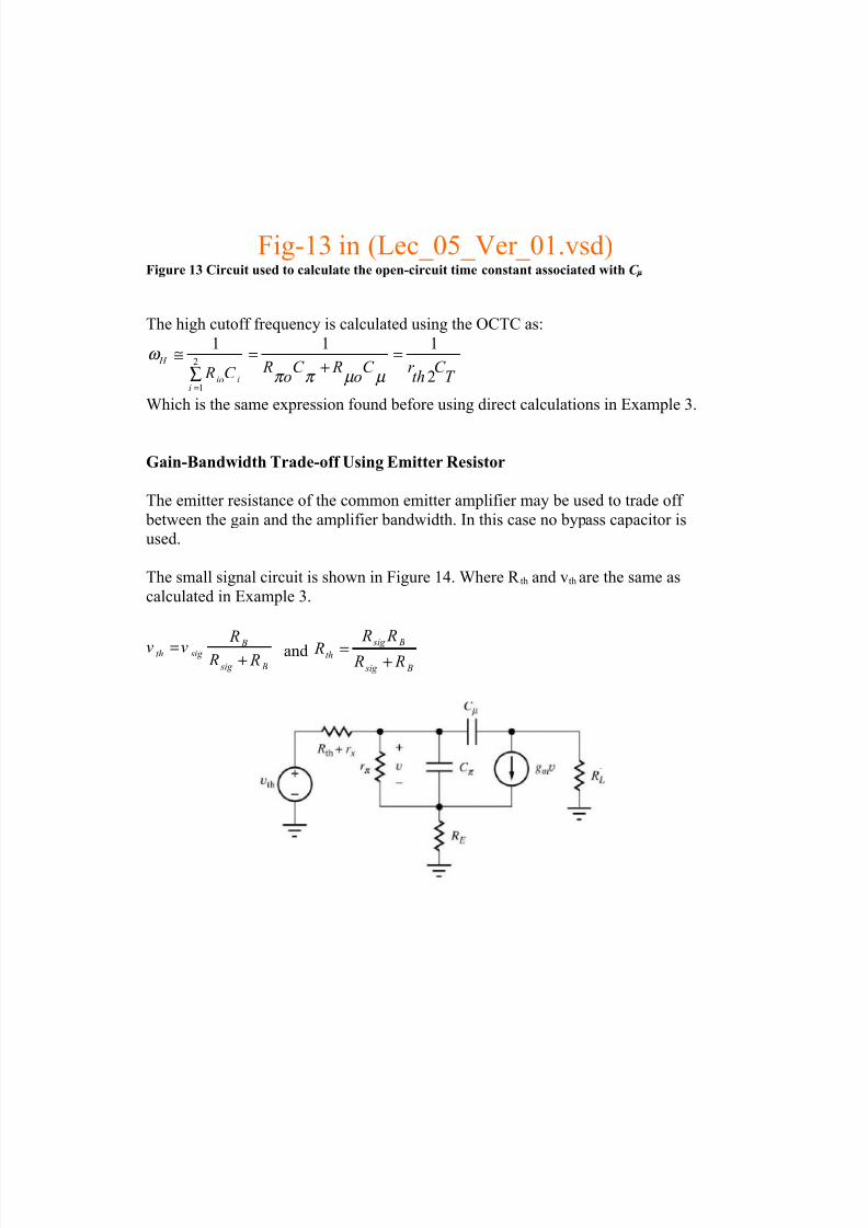
3ain-4and#idth Trade-off /sing Emitter Resistor
The emitter resistance of the common emitter amplifier may be used to trade off
between the gain and the amplifier bandwidth In this case no bypass capacitor is
used
The small signal circuit is shown in )igure &9 Ghere 2 th and vth are the same as
calculated in Example 6
Bth sig
sig B
Rv v
R R=
+ and sig B
th
sig B
R R R
R R=
+
8/13/2019 Lec 05 WFig Ver 01
http://slidepdf.com/reader/full/lec-05-wfig-ver-01 14/16
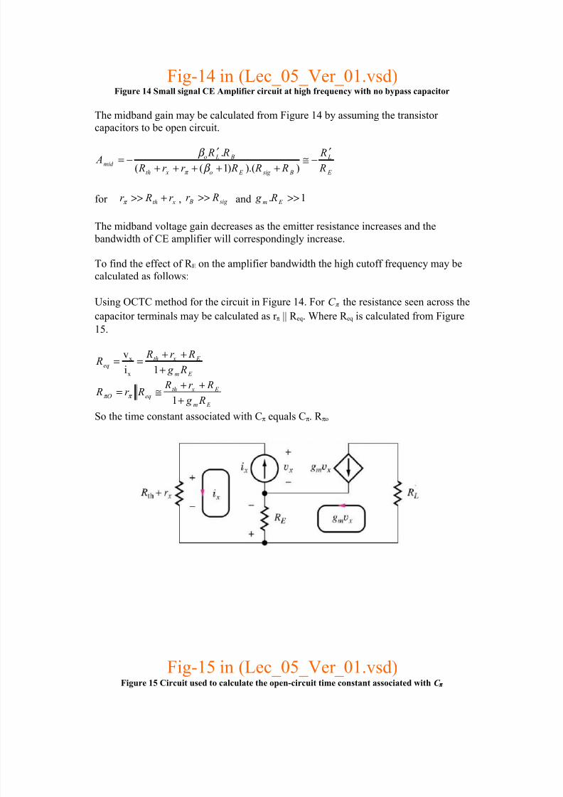
)ig$&9 in *+ec,-.,/er,-&vsd0Figure $ Small signal CE Amplifier circuit at high frequency #ith no ypass capacitor
The midband gain may be calculated from )igure &9 by assuming the transistor
capacitors to be open circuit
* * &0 0* 0
o L B Lmid
th x o E sig B E
R R R A
R r r R R R Rπ
β
β
′ ′= − ≅ −
+ + + + +
for th xr R r π >> + " B sig r R>> and &m E g R >>
The midband voltage gain decreases as the emitter resistance increases and the
bandwidth of CE amplifier will correspondingly increase
To find the effect of 2 E on the amplifier bandwidth the high cutoff frequency may becalculated as follows'
5sing OCTC method for the circuit in )igure &9 )or C π the resistance seen across the
capacitor terminals may be calculated as r π 44 2 eq Ghere 2 eq is calculated from )igure
&.
x
x
v
i &
th x E e'
m E
R r R R
g R
+ += =
+
&
th x E & e'
m E
R r R R r R
g Rπ π
+ += ≅
+#o the time constant associated with Cπ equals Cπ 2 πo
)ig$&. in *+ec,-.,/er,-&vsd0Figure % Circuit used to calculate the open-circuit time constant associated #ith C
8/13/2019 Lec 05 WFig Ver 01
http://slidepdf.com/reader/full/lec-05-wfig-ver-01 15/16
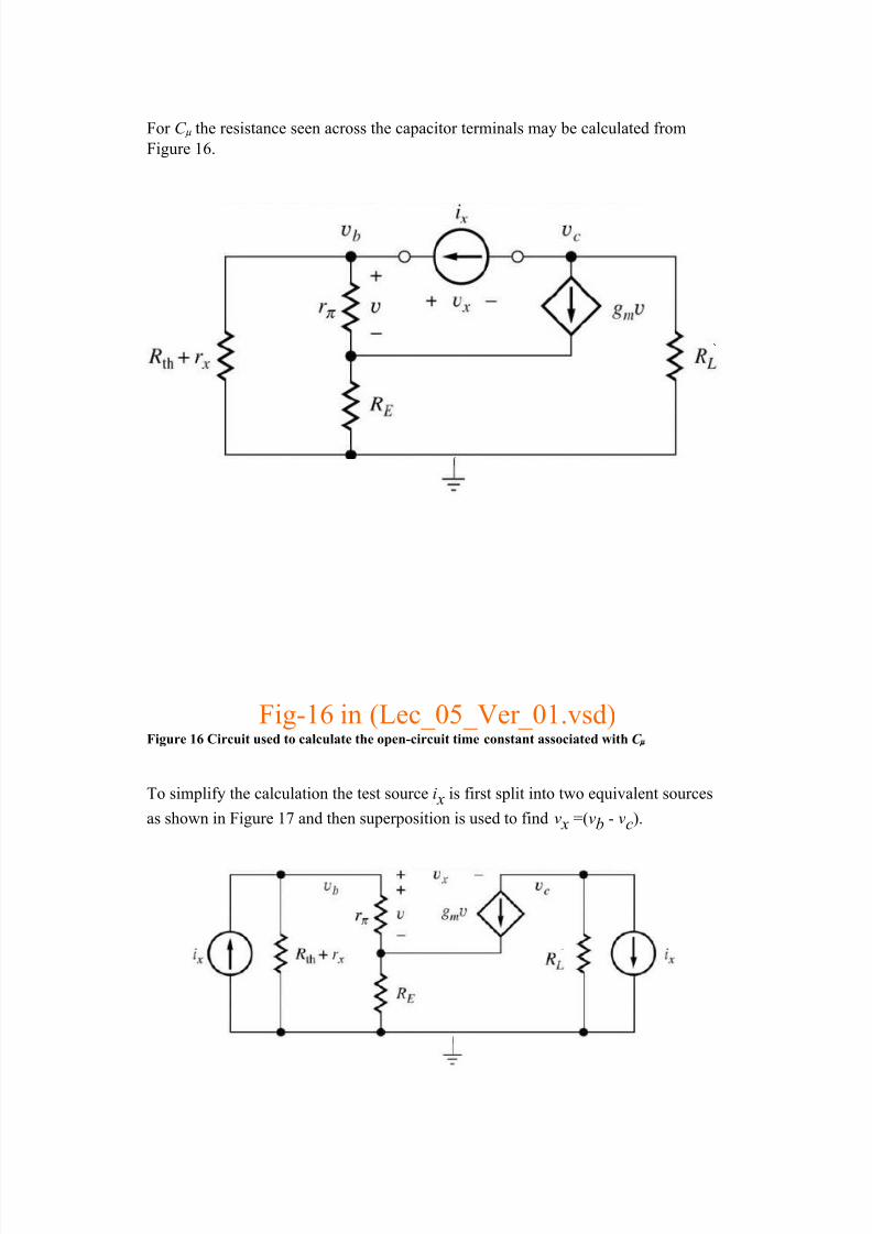
)or C µ the resistance seen across the capacitor terminals may be calculated from
)igure &8
)ig$&8 in *+ec,-.,/er,-&vsd0Figure & Circuit used to calculate the open-circuit time constant associated #ith C
To simplify the calculation the test source i x is first split into two equivalent sources
as shown in )igure &: and then superposition is used to find v x
<*vb
$ v(0

8/13/2019 Lec 05 WFig Ver 01
http://slidepdf.com/reader/full/lec-05-wfig-ver-01 16/16
)ig$&: in *+ec,-.,/er,-&vsd0Figure ' Modified circuit used to calculate the open-circuit time constant associated #ith C
!ssuming that β o AA& and ( ) ( )* &0th x o E R r r Rπ β + << + +
x
x
v* 0 &i &
m L Lo th x
m E th x
g R R R R r g R R r
µ
′ ′= = + + + ÷+ +
#o the time constant associated with Cµ equals Cµ 2 µo
The high cutoff frequency is calculated using the OCTC as'
1
&
& &
* 0 & && &
H
E m L Lio ith xi
m E th x m E th x
C R g R R R C R r C g R R r g R R r
π
ω
µ =
≅ = ′ ′∑ + + + + + ÷ ÷ ÷ ÷+ + + +
If we used the same amplifier discussed in Example 9 with C E<-
Ge will obtain'
6D81: //
&6
Lmid
E
R A
R
′ −≅ − = = −
@
&
* 0 & && &
&
1-8 &6 889@6D8 6D8
*-DD -1.0 & -. && 889@&6 -DD -1. & 889 &6 -DD -1.
1&&J radsec
H
E m L Lth x
m E th x m E th x
C R g R R R r C
g R R r g R R r
)*
k )*
π
ω
µ
≅ ′ ′
+ + + + + ÷ ÷ ÷ ÷+ + + +
=
+ Ω + + + + ÷ ÷ ÷+ + + + =
!s we can see we got a higher bandwidth on the expense of lower midband gain