Rev B, October 1998
Application Note 558 Ralph Locher
Introduction to Power MOSFETs and their Applications
INTRODUCTION
The Power MOSFETs that are available today perform the same function as Bipolar transistorsexcept the former are voltage controlled in contrast to the current controlled Bipolar devices. TodayMOSFETs owe their ever-increasing popularity to their high input impedance and to the fact thatbeing a majority carrier device, they do not suffer from minority carrier storage time effects, ther-mal runaway, or second breakdown.
MOSFET OPERATION
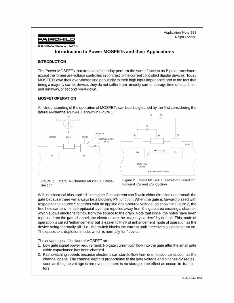
An Understanding of the operation of MOSFETs can best be gleaned by the first considering thelateral N-channel MOSFET shown in Figure 1.
With no electrical bias applied to the gate G, no current can flow in either direction underneath thegate because there will always be a blocking PN junction. When the gate is forward biased withrespect to the source S together with an applied drain-source voltage, as shown in Figure 2, thefree hole carriers in the p-epitaxial layer are repelled away from the gate area creating a channel,which allows electrons to flow from the source to the drain. Note that since the holes have beenrepelled from the gate channel, the electrons are the “majority carriers” by default. This mode ofoperation is called “enhancement” but is easier to think of enhancement mode of operation as thedevice being “normally off”, i.e., the switch blocks the current until it receives a signal to turn on.The opposite is depletion mode, which is normally “on” device.
The advantages of the lateral MOSFET are:1. Low gate signal power requirement. No gate current can flow into the gate after the small gate
oxide capacitance has been charged.2. Fast switching speeds because electrons can start to flow from drain to source as soon as the
channel opens. The channel depth is proportional to the gate voltage and pinches closed assoon as the gate voltage is removed, so there is no storage time effect as occurs in transistors.
N+
SOURCE GATE DRAIN
METAL (AL)
SILICON DIOXIDE(SiO )2
S D
G
BODY
N+
N+
SiO2
S DG
N+
RLVD
VG
INVERTEDZONE
ID
P BODY SUBSTRATE
Figure 1. Lateral N-Channel MOSFET Cross-Section
Figure 2. Lateral MOSFET Transistor Biased forForward Current Conduction

The major disadvantages are:1. High resistance channels. In normal operation, the source is electrically connected to the
substrate. With no gate bias, the depletion region extends out from the N+ drain in a pseudo-hemispherical shape. The channel length L cannot be made shorter than the minimum deple-tion width required to support the rated voltage of the device.
2. Channel resistance may be decreased by creating wider channels but this is costly since ituses up valuable silicon real estate. It also slows down the switching speed of the device byincreasing its gate capacitance.
Enter vertical MOSFETs!The Power MOSFET structure (also known as DMOS) is shown Figure 3.
The current path is created by inverting the p-layer underneath the gate by the identical method inthe lateral MOSFETs. Source current flows underneath this gate area and then vertically throughthe drain, spreading out as it flows down. A typical MOSFET consists of many thousands of N+sources conducting in parallel. This vertical geometry makes possible lower on-state resistances(RDS(on)) for the same blocking voltage and faster switching than the lateral MOSFETs.
There are many vertical construction designs possible, e.g., V-groove and U-groove, and manysource geometries, e.g. squares, triangles, hexagons, etc. The many considerations that deter-mine the source geometry are RDS(on), input capacitance, switching times and transconductance.
PARASITIC DIODE
Early versions of MOSFETs were susceptible to voltage breakdown due to voltage transients andalso had a tendency to turn on under high rates of rise of drain-to-source voltage (dV/dt). Bothresulted in catastrophic failures. The dV/dt turn-on was due to the inherent parasitic NPN transis-tor incorporated within the MOSFET, shown schematically in Figure 4a. Current flow needed tocharge up junction capacitance CDG acts like base current to turn on the parasitic NPN.
The parasitic NPN action is suppressed by shorting the N+ source to the P+ body using thesource metallization. This now creates an inherent PN diode anti-parallel to the MOSFET transis-tor (see Figure 4b). Because of its extensive junction area, the current ratings and thermalresistance of this diode exhibit a very long reverse recovery time and large reverse recovery currentdue to the long minority carrier lifetimes in the N-drain layer, which precludes the use of this
N- DRAIN
N+ SUBSTRATE
POLY SILICON GATE
N+
P-
P+
CURRENTFLOW
SOURCEMETALLIZATION
CHANNEL
GATE OXIDE
CHANNEL
P+
P- P-
N+N+ N+
DRAIN
Figure 3. Vertical DMOS Cross-Sectional
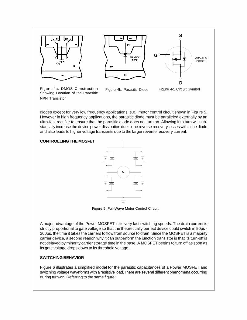
diodes except for very low frequency applications. e.g., motor control circuit shown in Figure 5.However in high frequency applications, the parasitic diode must be paralleled externally by anultra-fast rectifier to ensure that the parasitic diode does not turn on. Allowing it to turn will sub-stantially increase the device power dissipation due to the reverse recovery losses within the diodeand also leads to higher voltage transients due to the larger reverse recovery current.
CONTROLLING THE MOSFET
A major advantage of the Power MOSFET is its very fast switching speeds. The drain current isstrictly proportional to gate voltage so that the theoretically perfect device could switch in 50ps -200ps, the time it takes the carriers to flow from source to drain. Since the MOSFET is a majoritycarrier device, a second reason why it can outperform the junction transistor is that its turn-off isnot delayed by minority carrier storage time in the base. A MOSFET begins to turn off as soon asits gate voltage drops down to its threshold voltage.
SWITCHING BEHAVIOR
Figure 6 illustrates a simplified model for the parasitic capacitances of a Power MOSFET andswitching voltage waveforms with a resistive load.There are several different phenomena occurringduring turn-on. Referring to the same figure:
S
D
GPARASITIC
DIODE
M
Figure 4c. Circuit Symbol
Figure 5. Full-Wave Motor Control Circuit
Figure 4a. DMOS ConstructionShowing Location of the Parasitic
NPN Transistor
Figure 4b. Parasitic Diode
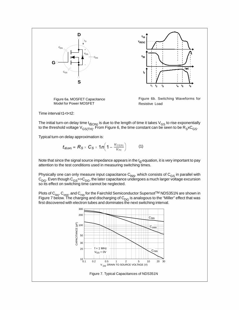
Time interval t1<t<t2:
The initial turn-on delay time td(ON) is due to the length of time it takes VGS to rise exponentiallyto the threshold voltage VGS(TH). From Figure 6, the time constant can be seen to be RSxCGS.
Typical turn-on delay approximation is:
(1)
Note that since the signal source impedance appears in the td equation, it is very important to payattention to the test conditions used in measuring switching times.
Physically one can only measure input capacitance Ciss, which consists of CGS in parallel withCDG. Even though CGS>>CDG, the later capacitance undergoes a much larger voltage excursionso its effect on switching time cannot be neglected.
Plots of Ciss, Coss, and Crss for the Fairchild Semiconductor SupersotTM NDS351N are shown inFigure 7 below. The charging and discharging of CDG is analogous to the “Miller” effect that wasfirst discovered with electron tubes and dominates the next switching interval.
S
D
G
DGC
GSC
DSCDSV
DI
+
-
Figure 6a. MOSFET CapacitanceModel for Power MOSFET
Figure 6b. Switching Waveforms for
Resistive Load
0.1 0.2 0.5 1 2 5 10 20 3010
20
30
50
100
200
300
V , DRAIN TO SOURCE VOLTAGE (V)
CA
PA
CIT
AN
CE
(pF
)
DS
C iss
f = 1 MHzV = 0VGS
C oss
C rss
Figure 7. Typical Capacitances of NDS351N

Time interval t2<t<t3:
Since VGS has now achieved the threshold value, the MOSFET begins to draw increasing loadcurrent and VDS decreases. CDG must not only discharge but its capacitance value also increasessince it is inversely proportional to VDS, namely:
(2)
Unless the gate driver can quickly supply the current required to discharged CDG, voltage fall willbe slowed with increases in turn-on time.
Time interval t3<t<t4:
The MOSFET is now on so the gate voltage can rise to the overdrive level.
Turn-off interval t4<t<t6:
Turn-off occurs in reverse order. VGS must drop back close to the threshold value before RDS(on)will start to increase. As VDS starts to rise, the Miller effect due to CDG re-occurs and impedes therise of VDS as CDG recharges to VCC.
Specific gate drive circuits for different applications are discussed and illustrated later in thispaper.
MOSFET CHARACTERIZATION
The output characteristics (ID vs VDS) of the Fairchild Semiconductor SupersotTM NDS351N areillustrated in Figures 8 and 9. The two distinct regions of operation in Figure 8 have been labeled“linear” and “saturated”. To understand the difference, recall that the actual current path in aMOSFET is horizontal through the channel created under the gate oxide and then vertical throughthe drain. In the linear region of operation, the voltage across the MOSFET channel is notsufficient for the carriers to reach their maximum current density. The static RDS(on), definedsimply as VDS/IDS, is a constant.
As VDS is increased, the carriers reach their maximum drift velocity and the current amplitudecannot increase. Since the device is behaving like a current generator, it is said to have high outputimpedance. This is the so-called “saturation” regions. One should also note that in comparingMOSFET operation to Bipolar transistor, the linear and saturated regions are just the opposite tothe MOSFET. The equal spacing between the output ID curves for constant step in VGS indicatesthat the transfer characteristics in Figure 9 will be linear in the saturated region.
Figure 8. NDS351N Output Characteristics Figure 9. NDS351N Transfer Characteristics
IMPORTANCE OF THRESHOLD VOLTAGE
Threshold voltage VGS(th) is the minimum gate voltage that initiates drain current flow. VGS(th) canbe easily measured on a Tektronix 576 curve tracer by connecting the gate to the drain andrecording the required drain voltage for a specified drain current, typically 250µA. VGS(th) in Figure9 is 1.6V. While a high value of VGS(th), can apparently lengthen turn-on delay time, a low value forPower MOSFET is undesirable for the following reasons:
1. VGS(th) decreases with increased temperature.2. The high gate impedance of a MOSFET makes it susceptible to spurious turn-on due to gatenoise.3. One of the more common modes of failure is gate-oxide voltage punch-through. Low VGS(th)requires thinner oxides, which lowers the gate oxide voltage rating.
POWER MOSFET THERMAL MODEL
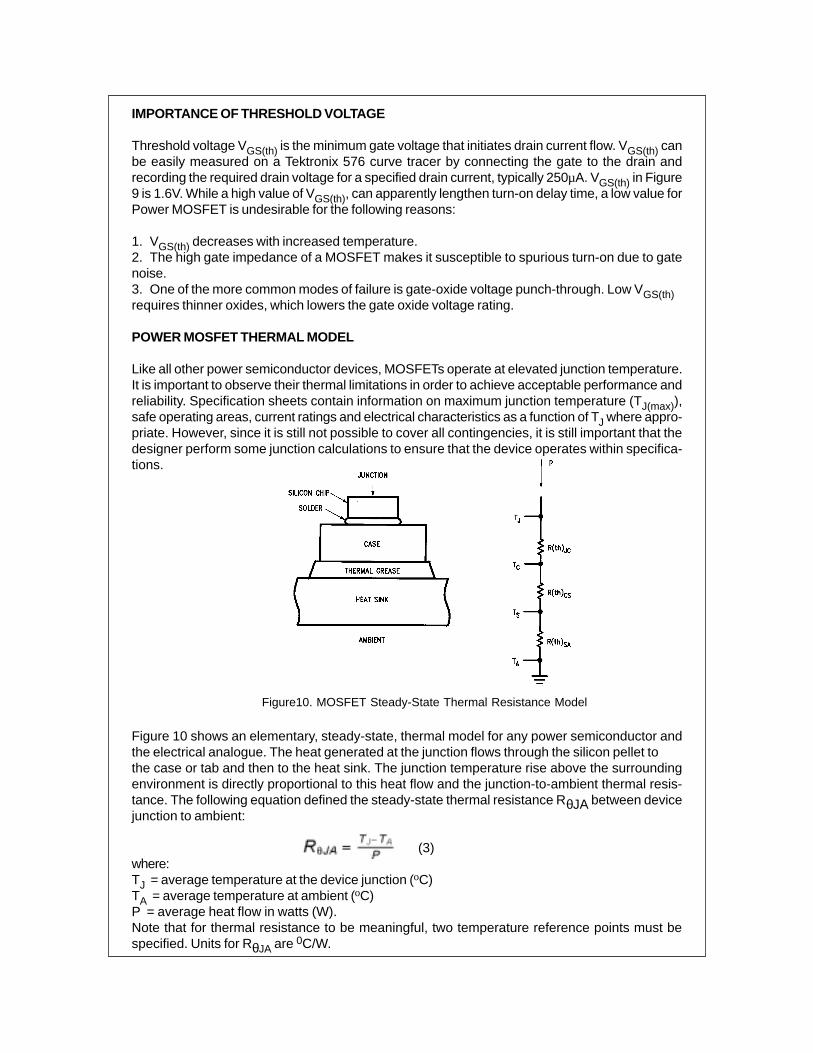
Like all other power semiconductor devices, MOSFETs operate at elevated junction temperature.It is important to observe their thermal limitations in order to achieve acceptable performance andreliability. Specification sheets contain information on maximum junction temperature (TJ(max)),safe operating areas, current ratings and electrical characteristics as a function of TJ where appro-priate. However, since it is still not possible to cover all contingencies, it is still important that thedesigner perform some junction calculations to ensure that the device operates within specifica-tions.
Figure 10 shows an elementary, steady-state, thermal model for any power semiconductor andthe electrical analogue. The heat generated at the junction flows through the silicon pellet tothe case or tab and then to the heat sink. The junction temperature rise above the surroundingenvironment is directly proportional to this heat flow and the junction-to-ambient thermal resis-tance. The following equation defined the steady-state thermal resistance RθJA between devicejunction to ambient:
(3)where:TJ = average temperature at the device junction (oC)TA = average temperature at ambient (oC)P = average heat flow in watts (W).Note that for thermal resistance to be meaningful, two temperature reference points must bespecified. Units for RθJA are 0C/W.
Figure10. MOSFET Steady-State Thermal Resistance Model
The thermal model shows symbolically the locations for the reference points of junction tempera-ture, case temperature, sink temperature and ambient temperature. These temperature referencedefine the following thermal resistances:
RθJC: Junction-to-Case thermal resistance.RθCS: Case-to-Sink thermal resistance.RθSA:Sink-to-Ambient thermal resistance.
Since the thermal resistances are in series:
(4)
The design and manufacture of the device determines RθJC so that while RθJC will vary somewhatfrom device to device, it is the SOLE RESPONSIBILITY of the manufacturer to guarantee a maxi-mum value for RθJC. Both the user and manufacturer must cooperate in keeping RθCS to anacceptable maximum. Finally, the user has sole responsibility for the external heat sinking.By inspection of Figure 10, one can write an expression for TJ:
(5)
While this appears to be a very simple formula, the major problem using it is due to the fact thatthe power dissipated by the MOSFET depends upon TJ. Consequently one must use either aniterative or graphical solution to find the maximum RθSA to ensure stability. But an explanation oftransient thermal resistance is in order to handle the case of pulsed applications.
Use of steady-state thermal resistance is not satisfactory for finding peak junction temperaturesfor pulsed applications. Plugging in the peak power value results in overestimating the actualjunction temperature while using the average power value underestimates the peak junction tem-perature at the end of the power pulse. The reason for the discrepancy lies in the thermal capacityof the semiconductor and its housing, i.e., its ability to store heat and to cool down before the nextpulse.
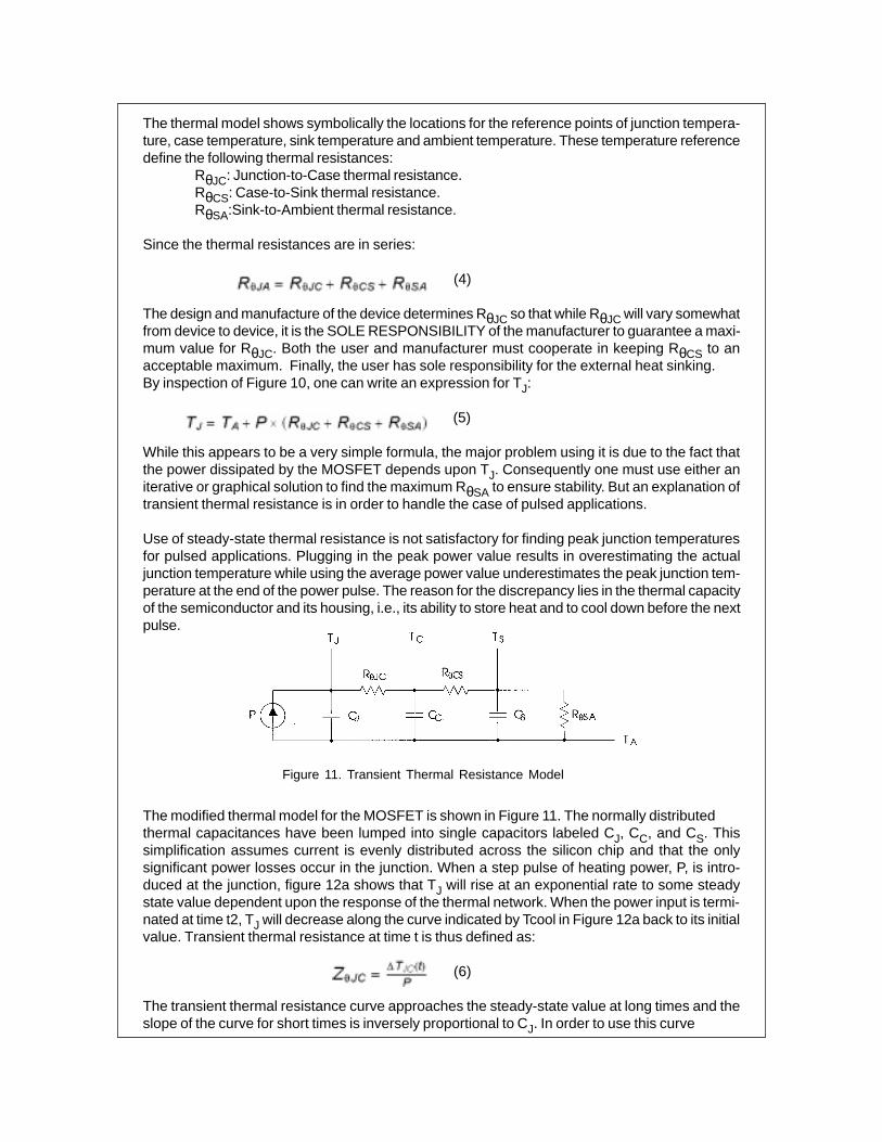
The modified thermal model for the MOSFET is shown in Figure 11. The normally distributedthermal capacitances have been lumped into single capacitors labeled CJ, CC, and CS. Thissimplification assumes current is evenly distributed across the silicon chip and that the onlysignificant power losses occur in the junction. When a step pulse of heating power, P, is intro-duced at the junction, figure 12a shows that TJ will rise at an exponential rate to some steadystate value dependent upon the response of the thermal network. When the power input is termi-nated at time t2, TJ will decrease along the curve indicated by Tcool in Figure 12a back to its initialvalue. Transient thermal resistance at time t is thus defined as:
(6)
The transient thermal resistance curve approaches the steady-state value at long times and theslope of the curve for short times is inversely proportional to CJ. In order to use this curve
Figure 11. Transient Thermal Resistance Model

Figure 13c. Junction Temperature Response
to Individual Power PulseFigure 13d. Use of Superposition to Determine
Peak TJ
with confidence, it must represent the highest values ZθJC for each time interval that can beexpected from the manufacturing distribution of the products.
While predicting TJ in response to a series of power pulses becomes very complex, superpositionof power pulses offers a rigorous numerical method of using the transient thermal resistance curveto secure a solution. Superposition tests the response of a network to any input function byreplacing the input with an equivalent series of superimposed positive and negative step functions.Each step function must start from zero and continue to the time for which TJ is to be computed.For example, Figure 13 illustrates a typical train of heating pulses.
TJ at time is given by:
(7)
The typical use condition is to compute the peak junction temperature at thermal equilibrium for atrain of equal amplitude power pulses as shown in Figure 14.
Figure 12a. Junction Temperature Response to a
Step Pulse of Heating Power
Figure 12b. Transient Thermal Resistance Curve
for NDS351N
Figure 13a. Heat Input Figure 13b. Equivalent Heat Input by
Superposition of Power Pulses
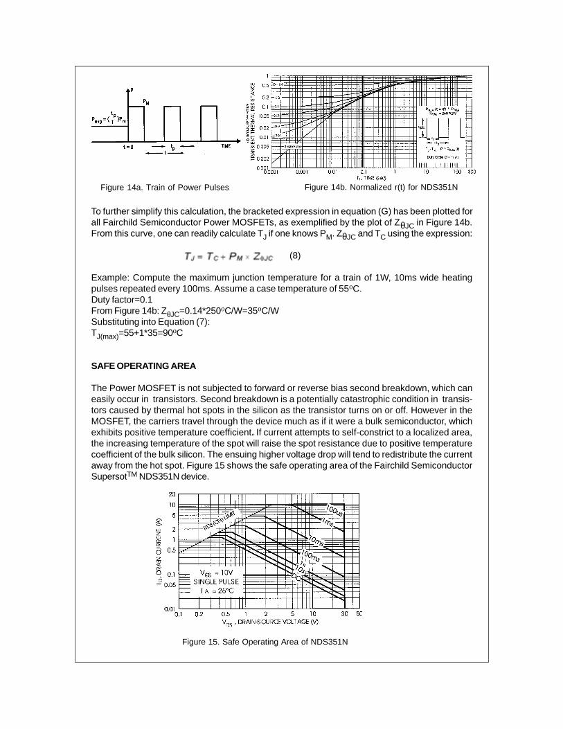
To further simplify this calculation, the bracketed expression in equation (G) has been plotted forall Fairchild Semiconductor Power MOSFETs, as exemplified by the plot of ZθJC in Figure 14b.From this curve, one can readily calculate TJ if one knows PM. ZθJC and TC using the expression:
(8)
Example: Compute the maximum junction temperature for a train of 1W, 10ms wide heatingpulses repeated every 100ms. Assume a case temperature of 55oC.Duty factor=0.1From Figure 14b: ZθJC=0.14*250oC/W=35oC/WSubstituting into Equation (7):TJ(max)=55+1*35=90oC
SAFE OPERATING AREA
The Power MOSFET is not subjected to forward or reverse bias second breakdown, which caneasily occur in transistors. Second breakdown is a potentially catastrophic condition in transis-tors caused by thermal hot spots in the silicon as the transistor turns on or off. However in theMOSFET, the carriers travel through the device much as if it were a bulk semiconductor, whichexhibits positive temperature coefficient. If current attempts to self-constrict to a localized area,the increasing temperature of the spot will raise the spot resistance due to positive temperaturecoefficient of the bulk silicon. The ensuing higher voltage drop will tend to redistribute the currentaway from the hot spot. Figure 15 shows the safe operating area of the Fairchild SemiconductorSupersotTM NDS351N device.
Figure 14a. Train of Power Pulses Figure 14b. Normalized r(t) for NDS351N
Figure 15. Safe Operating Area of NDS351N
Note that the safe area boundaries are only thermally limited and exhibit no derating for secondbreakdown. This shows that while the MOSFET transistor is very rugged, it may still be destroyedthermally by forcing it to dissipate too much power.
ON-RESISTANCE RDS(on)
The on-resistance of a Power MOSFET is a very important parameter because it determines howmuch current the device can carry for low to medium frequency (less than 200kHz) applications.After being turned on, the on-state is defined simply as its on-state voltage divided by on-statecurrent. When conducting current as a switch, the conduction losses P are:
(9)
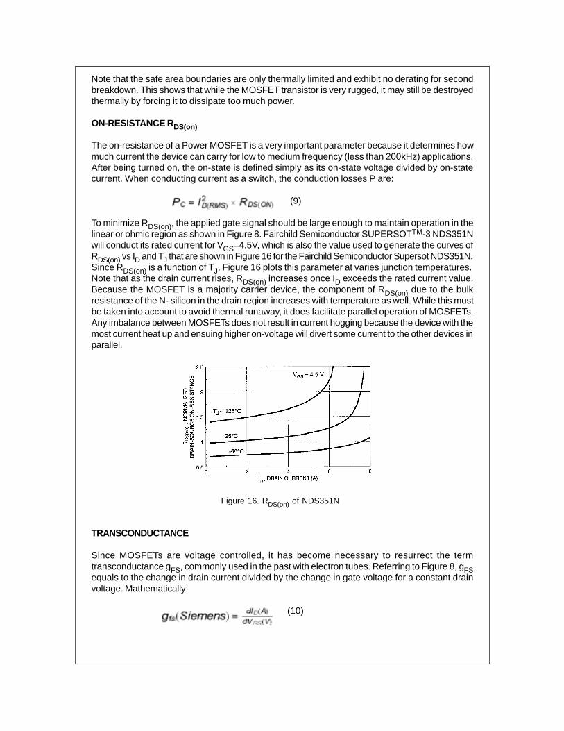
To minimize RDS(on), the applied gate signal should be large enough to maintain operation in thelinear or ohmic region as shown in Figure 8. Fairchild Semiconductor SUPERSOTTM-3 NDS351Nwill conduct its rated current for VGS=4.5V, which is also the value used to generate the curves ofRDS(on) vs ID and TJ that are shown in Figure 16 for the Fairchild Semiconductor Supersot NDS351N.Since RDS(on) is a function of TJ, Figure 16 plots this parameter at varies junction temperatures.Note that as the drain current rises, RDS(on) increases once ID exceeds the rated current value.Because the MOSFET is a majority carrier device, the component of RDS(on) due to the bulkresistance of the N- silicon in the drain region increases with temperature as well. While this mustbe taken into account to avoid thermal runaway, it does facilitate parallel operation of MOSFETs.Any imbalance between MOSFETs does not result in current hogging because the device with themost current heat up and ensuing higher on-voltage will divert some current to the other devices inparallel.
TRANSCONDUCTANCE
Since MOSFETs are voltage controlled, it has become necessary to resurrect the termtransconductance gFS, commonly used in the past with electron tubes. Referring to Figure 8, gFSequals to the change in drain current divided by the change in gate voltage for a constant drainvoltage. Mathematically:
(10)
Figure 16. RDS(on) of NDS351N

Transconductance varies with operating conditions, starting at 0 for VGS<VGS(th) and peaking at afinite value when the device is fully saturated. It is very small in the ohmic region because thedevice cannot conduct any more current. Transconductance is useful in designing linear amplifiersand does not have any significance in switching power supplies.
GATE DRIVE CIRCUITS FOR POWER MOSFETs
The drive circuit for a Power MOSFET will affect its switching behavior and its power dissipation.Consequently the type of drive circuitry depends upon the application. If on-state power lossesdue to RDS(on), will predominate, there is little point in designing a costly drive circuit. This powerdissipation is relatively independent of gate drive as long as the gate-source voltage exceeds thethreshold voltage by several volts and an elaborate drive circuit to decrease switching times willonly create additional EMI and voltage ringing. In contrast, the drive circuit for a device switching at200KHz or more will affect the power dissipation since switching losses are a significant part ofthe total power dissipation.
Compare to a junction transistor, the switching losses in a MOSFET can be made much smallerbut these losses must still be taken into consideration. Examples of several typical loads alongwith the idealized switching waveforms and expressions for power dissipation are given in Figure17 to 19.
Their power losses can be calculated from the general expression:
(11)
where fS =Switching frequency.
For the idealized waveforms shown in the figures, the integration can be approximated by thecalculating areas of triangles:Resistive loads:
Inductive Load:
Figure17. Resistive Load
Switching Waveforms
Figure18. Clamped Inductive
Load Switching WaveformsFigure19. Capacitive Load
Switching Waveforms
where PC = conduction loss during period T.

Capacitive load:
Gate losses and blocking losses can usually be neglected. Using these equations, circuit de-signer is able to estimate the required heat sink. A final heat run in a controlled temperatureenvironment is necessary to ensure thermal stability.
Since a MOSFET is essentially voltage controlled, the only gate current required is that neces-sary to charge the input capacitance Ciss. In contrast to a 10A transistor, which may require abase current of 2A to ensure saturation, a Power MOSFET can be driven directly by CMOS oropen-collector TTL logic circuit similar to that in Figure 20.
Turn-on speed depends upon the selection of resistor R1, whose minimum value will be deter-mined by the current sinking rating of the IC. It is essential that an open collector TTL buffer beused since the voltage applied to the gate must exceed the MOSFET threshold voltage. CMOSdevices can be used to drive the power device directly since they are capable of operating 15Vsupplies.
Interface ICs, originally intended for other applications, can be used to drive the Power MOSFETs,as shown below in Figure 21.
Figure 20. Open Collector TTL Drive Circuit
Figure 21. Interface ICs Used to Drive Power MOSFETs

Most frequently, switching power supply applications employ a pulse width modulator IC with anNPN transistor output stage. This output transistor is ON when the MOSFET should be ON,hence the type of drive used with open-collector TTL devices cannot be used. Figures 22 and 23give examples of typical drive circuits used with PWM ICs.
Isolation: Off-line switching power supplies use power MOSFETs in a half bridge configurationbecause inexpensive, high voltage devices with low RDS(on) are not available.
Since one of the power devices is connected to the positive rail, its drive circuitry is also floating ata high potential. The most versatile method of coupling the drive circuitry is to use a pulse trans-former. Pulse transformers are also normally used to isolate the logic circuitry from the MOSFETsoperating at high voltage to protect it from a MOSFET failure.
The zener diodes shown in Figure 25 is included to reset the pulse transformer quickly. The dutycycle can approach 50% with a 12V zener diode. For better performance at turn-off, a PNPtransistor can be added as shown in Figure 26.
Figure 27 illustrates an alternate method to reverse bias the MOSFET during turn-off by insertinga capacitor in series with the pulse transformer. The capacitor also ensures that the pulse trans-former will not saturate due to DC bias.
Figure 22. Circuit for PWM IC Driving MOSFET.
The PNP Transistor Speeds Up Turn-Off
Figure 23. Emitter Follower with Speed-Up
Capacitor
Figure 24. Half-Bridge Configuration Figure 25. Simple Pulse Transformer Drive Circuit.The Transistor May Be a Part of a PWM IC if Appli-
cable

Opto-isolators may also be used to drive power MOSFETs but their long switching times makethem suitable only for low frequency applications.
SELECTING A DRIVE CIRCUIT
Any of the circuits shown are capable of turning a Power MOSFET on and off. The type of circuitdepends upon the application. The current sinking and sourcing capabilities of the drive circuit willdetermine the switching time and switching losses of the power device. As a rule, the higher thegate current at turn-on and turn-off, the lower the switching losses will be. However, fast drivecircuits may produce ringing in the gate circuit and drain circuits. At turn-on, ringing in the gatecircuit may produce a voltage transient in excess of the maximum VGS rating, which will puncturethe gate oxide and destroy it. To prevent this occurrence, a zener diode of appropriate value maybe added to the circuit as shown in Figure 28. Note that the zener should be mounted as close aspossible to the device.
At turn-off, the gate voltage may ring back up to the threshold voltage and turn on the device for ashort period. There is also the possibility that the drain-source voltage will exceed itsmaximum rated voltage due to ringing in the drain circuit. A protective RC snubber circuit or zenerdiode may be added to limit drain voltage to a safe level.
Figure 26. Improved Performance at Turn-Off
with a TransistorFigure 27. Emitter Follower Driver with Speed-
Up Capacitor
Figure 28. Zener Diode to Prevent Excessive Gate-Source Voltages

TRADEMARKS
ACEx™CoolFET™CROSSVOLT™E2CMOSTM
FACT™FACT Quiet Series™FAST®
FASTr™GTO™HiSeC™
The following are registered and unregistered trademarks Fairchild Semiconductor owns or is authorized to use and isnot intended to be an exhaustive list of all such trademarks.
LIFE SUPPORT POLICY
FAIRCHILD’S PRODUCTS ARE NOT AUTHORIZED FOR USE AS CRITICAL COMPONENTS IN LIFE SUPPORTDEVICES OR SYSTEMS WITHOUT THE EXPRESS WRITTEN APPROVAL OF FAIRCHILD SEMICONDUCTOR CORPORATION.As used herein:
ISOPLANAR™MICROWIRE™POP™PowerTrench™QS™Quiet Series™SuperSOT™-3SuperSOT™-6SuperSOT™-8TinyLogic™
1. Life support devices or systems are devices orsystems which, (a) are intended for surgical implant intothe body, or (b) support or sustain life, or (c) whosefailure to perform when properly used in accordancewith instructions for use provided in the labeling, can bereasonably expected to result in significant injury to theuser.
2. A critical component is any component of a lifesupport device or system whose failure to perform canbe reasonably expected to cause the failure of the lifesupport device or system, or to affect its safety oreffectiveness.
PRODUCT STATUS DEFINITIONS
Definition of Terms
Datasheet Identification Product Status Definition
Advance Information
Preliminary
No Identification Needed
Obsolete
This datasheet contains the design specifications forproduct development. Specifications may change inany manner without notice.
This datasheet contains preliminary data, andsupplementary data will be published at a later date.Fairchild Semiconductor reserves the right to makechanges at any time without notice in order to improvedesign.
This datasheet contains final specifications. FairchildSemiconductor reserves the right to make changes atany time without notice in order to improve design.
This datasheet contains specifications on a productthat has been discontinued by Fairchild semiconductor.The datasheet is printed for reference information only.
Formative orIn Design
First Production
Full Production
Not In Production
DISCLAIMER
FAIRCHILD SEMICONDUCTOR RESERVES THE RIGHT TO MAKE CHANGES WITHOUT FURTHERNOTICE TO ANY PRODUCTS HEREIN TO IMPROVE RELIABILITY, FUNCTION OR DESIGN. FAIRCHILDDOES NOT ASSUME ANY LIABILITY ARISING OUT OF THE APPLICATION OR USE OF ANY PRODUCTOR CIRCUIT DESCRIBED HEREIN; NEITHER DOES IT CONVEY ANY LICENSE UNDER ITS PATENTRIGHTS, NOR THE RIGHTS OF OTHERS.
©2002 Fairchild Semiconductor Corporation Application Note 7513 Rev. A1
Parallel Operation Of Semiconductor Switches
In uninterruptable power supplies demands for current han-dling capability to meet load current In uninterruptable powersupplies demands for current handling capability to meetload current requirements plus margins for overload and reli-ability purposes often exceed the capability of the largestsemiconductor device type considered and paralleling maybecome an attractive alternative. All switching power semi-conductors starting with SCR’s [1], bipolar transistors [2-4]
darlingtons [5] and field effect transistors [6-10], have beensuccessfully paralleled, but proper precaution had to betaken. We will review some of these methods, describe thecharacteristics of the insulated gate transistors, and showthe proper methods to operate this relatively new family ofdevices in parallel.
All semiconductor circuits using parallel connected devicesto switch a higher load current can easily be analyzed byusing Kirchoff’s law. As long as all voltage drops in the paral-lel branches are equal, the currents through the branchesare equal.
This sounds sensible and logical, but as soon as we con-sider the different stages every switching device has toassume and we consider the parameters of each switchingdevice which guarantees equal voltage drops in thebranches over the required temperature range and over theduration of the switching cycle, complications begin toappear.
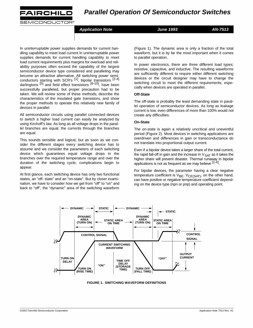
At first glance, each switching device has only two functionalstates, an “off- state” and an “on-state”. But by closer exami-nation, we have to consider how we get from “off” to “on” andback to “off”, the “dynamic” area of the switching waveform
(Figure 1). The dynamic area is only a fraction of the totalwaveform, but it is by far the most important when it comesto parallel operation.
In power electronics, there are three different load types;resistive, capacitive, and inductive. The resulting waveformsare sufficiently different to require either different switchingdevices or the circuit designer may have to change theswitching circuit to meet the different requirements, espe-cially when devices are operated in parallel.
Off-State
The off-state is probably the least demanding state in paral-lel operation of semiconductor devices. As long as leakagecurrent is low, even differences of more than 100% would notcreate any difficulties.
On-State
The on-state is again a relatively uncritical and uneventfulperiod (Figure 2). Most devices in switching applications areoverdriven and differences in gain or transconductance donot translate into proportional output current.
Even if a bipolar device takes a larger share of the total current,the rapid fall-off in gain and the increase in VSAT as it takes thehigher share will prevent disaster. Thermal runaway in bipolarapplications is not as frequent as we may believe [2-4].
For bipolar devices, the parameter having a clear negativetemperature coefficient is VBE. VCE(SAT), on the other hand,can have positive or negative temperature coefficient depend-ing on the device type (npn or pnp) and operating point.
FIGURE 1. SWITCHING WAVEFORM DEFINITIONS
CONTROL
SIGNAL
OUTPUTCURRENT“OFF”
STATIC
TURN ONDELAY
CONTROL SIGNAL
CURRENT SWITCHINGWAVEFORM
“ON”TURN OFF
(FALL TIME)
TIME OFFDELAY
(STORAGETIME)TURN ON
(RISE TIME)
DYNAMICAREA
(TURN ON)
DYNAMIC
STATIC AREAON TIME
STATIC DYNAMIC
DYNAMICAREA
(TURN ON)STATIC AREA
ON TIME
Application Note June 1993 AN-7513
/Title AN753)Sub-ect Paral-el pera-
ion Of emi-on-uctor witch
)Autho ()Key-ords
Inter-il orpo-
ation,emi-on-uctor, va-
anche nergy ated, witch
ng ower up-lie, ower witch
ng
©2002 Fairchild Semiconductor Corporation Application Note 7513 Rev. A1
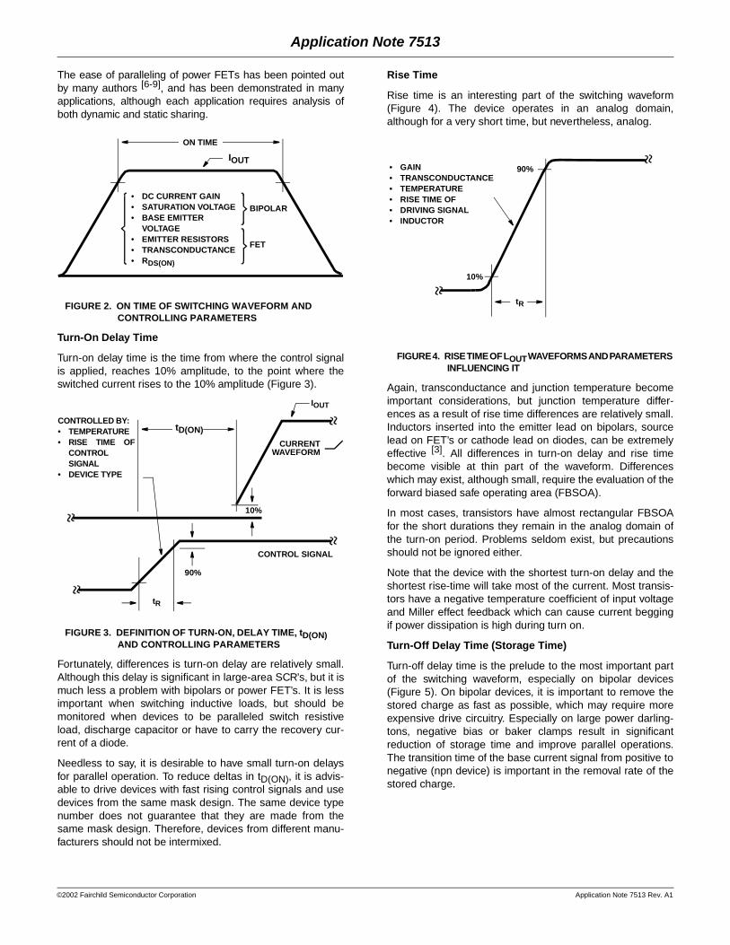
The ease of paralleling of power FETs has been pointed outby many authors [6-9], and has been demonstrated in manyapplications, although each application requires analysis ofboth dynamic and static sharing.
FIGURE 2. ON TIME OF SWITCHING WAVEFORM ANDCONTROLLING PARAMETERS
Turn-On Delay Time
Turn-on delay time is the time from where the control signalis applied, reaches 10% amplitude, to the point where theswitched current rises to the 10% amplitude (Figure 3).
FIGURE 3. DEFINITION OF TURN-ON, DELAY TIME, tD(ON) AND CONTROLLING PARAMETERS
Fortunately, differences is turn-on delay are relatively small.Although this delay is significant in large-area SCR’s, but it ismuch less a problem with bipolars or power FET’s. It is lessimportant when switching inductive loads, but should bemonitored when devices to be paralleled switch resistiveload, discharge capacitor or have to carry the recovery cur-rent of a diode.
Needless to say, it is desirable to have small turn-on delaysfor parallel operation. To reduce deltas in tD(ON), it is advis-able to drive devices with fast rising control signals and usedevices from the same mask design. The same device typenumber does not guarantee that they are made from thesame mask design. Therefore, devices from different manu-facturers should not be intermixed.
Rise Time
Rise time is an interesting part of the switching waveform(Figure 4). The device operates in an analog domain,although for a very short time, but nevertheless, analog.
FIGURE 4. RISE TIME OF LOUT WAVEFORMS AND PARAMETERS INFLUENCING IT
Again, transconductance and junction temperature becomeimportant considerations, but junction temperature differ-ences as a result of rise time differences are relatively small.Inductors inserted into the emitter lead on bipolars, sourcelead on FET’s or cathode lead on diodes, can be extremelyeffective [3]. All differences in turn-on delay and rise timebecome visible at thin part of the waveform. Differenceswhich may exist, although small, require the evaluation of theforward biased safe operating area (FBSOA).
In most cases, transistors have almost rectangular FBSOAfor the short durations they remain in the analog domain ofthe turn-on period. Problems seldom exist, but precautionsshould not be ignored either.
Note that the device with the shortest turn-on delay and theshortest rise-time will take most of the current. Most transis-tors have a negative temperature coefficient of input voltageand Miller effect feedback which can cause current beggingif power dissipation is high during turn on.
Turn-Off Delay Time (Storage Time)
Turn-off delay time is the prelude to the most important partof the switching waveform, especially on bipolar devices(Figure 5). On bipolar devices, it is important to remove thestored charge as fast as possible, which may require moreexpensive drive circuitry. Especially on large power darling-tons, negative bias or baker clamps result in significantreduction of storage time and improve parallel operations.The transition time of the base current signal from positive tonegative (npn device) is important in the removal rate of thestored charge.
ON TIME
IOUT
• DC CURRENT GAIN• SATURATION VOLTAGE• BASE EMITTER
VOLTAGE• EMITTER RESISTORS• TRANSCONDUCTANCE• RDS(ON)
BIPOLAR
FET
tD(ON)
IOUT
CURRENTWAVEFORM
10%
CONTROL SIGNAL
90%
tR
CONTROLLED BY:• TEMPERATURE• RISE TIME OF
CONTROLSIGNAL
• DEVICE TYPE
tR
10%
90%• GAIN• TRANSCONDUCTANCE• TEMPERATURE• RISE TIME OF• DRIVING SIGNAL• INDUCTOR
Application Note 7513

©2002 Fairchild Semiconductor Corporation Application Note 7513 Rev. A1
FIGURE 5. TURN-OFF WAVEFORM AND PARAMETERSINFLUENCING IT
Fall Time
Parameters which reduce storage time will also reduce falltime (Figure 6). For paralleled devices, differences in turn-offdelay or storage time will have a noticeable effect on falltime.
When inductive loads are turned off, the reverse biased safeoperating area (RBSOA) must be considered on bipolardevices. Hot spot formation [11] which results in suddenreduction of the VBE and further increase in IB could result inpermanent damage.
FIGURE 6. FALL TIME AND INFLUENCING PARAMETERS
The Insulated Gate Transistor
The insulated gate transistor (IGT) combines the high inputimpedance, voltage controlled turn on/turn off capabilities ofpower MOSFETs and the low on-state conduction losses ofbipolar transistors, making it an ideal device for many powerelectronics switching control applications.
IGT Structure and Operation
The basic device structure is illustrated by the unit cell crosssection of Figure 7. Like the MOSFET, the IGT consists ofmany individual cells connected in parallel. Processing of theIGT is similar to the vertical D-MOS technology used inMOSFETs. In the steady state, the n-channel IGT may bemodeled as a bipolar pnp driven by an n-channel MOSFET.The MOSFET supplies base current to the pnp thus theMOSFETs gate voltage controls the total current.
FIGURE 7. UNIT CELL CROSS SECTION AND STEADY STATE EQUIVALENT CIRCUIT OF IGT TRANSISTOR.
In normal operation, the emitter is grounded, the collectorbiased positive and with no gate-emitter voltage applied; J1is reverse biased. The device is in the forward blockingmode. When a positive voltage is applied to the gate withrespect to the emitter, an inversion channel is formed underthe gate and MOSFET current flows from the n+ sourceregion into the n-epi-layer to become the base current for thepnp. Junction J2 becomes forward biased and the deviceenters the conduction state. Holes are injected from the bot-
90%
CONTROL SIGNAL
NEGATIVEBIAS
TRANSITIONTIME
O-LINE
90%
tD(OFF)
POWER FETHOW FAST CANC’s BE DISCHARGED
BIPOLAR CONTROLLEDBY:• STORED CHARGE• STATE OF
SATURATION• NEGATIVE BIAS• TEMPERATURE
tFALL
90%
10%
BIPOLAR:STORED CHARGE REMOVALRATE OF CONTROL SIGNALNEGATIVE BIAS (TRANSITIONTIME) SATURATION VOLTAGETEMPERATURE.
FET:RDS(ON) CAPACITANCEOF FET DISCHARGEIMPEDANCE (TIMECONSTANT)
POLYSILICONGATE
EMITTER
n+ n+ n+ n+p-
p+ p+ p+CHANNEL
J1
WELL
n- EPITAXIAL LAYER
RMOD
J2
COLLECTOR
SUBSTRATEp+
BUFFER LAYERn+
UNIT CELL STRUCTURE
STEADYSTATEEQUIV.
CIRCUIT
C
PNP
RMOD
NMOSG
Application Note 7513

©2002 Fairchild Semiconductor Corporation Application Note 7513 Rev. A1
tom percent region into the n-epi-layer. The injected minoritycarrier density is 100 to 1000 times higher that the dopinglevel of the n-type epi-region. This conductivity modulationallows the IGT to operate at a forward conduction currentdensity 20 times that of an equivalent MOSFET. It is prima-rily in the thick epi, high-voltage devices where conductivitymodulation has its major impact to reduce on-resistance.
The typical output characteristics and the symbol of the IGTare shown in Figure 8. Like on MOSFETs, the output charac-teristics curves are generated by plotting collector emittercurrents, collector emitter voltage. Unlike the MOSFET, thereis an offset voltage generated by the collector emitter junc-tion of the npn-transistor. However, once this offset is over-come, the effective on-resistance in the saturation region ismuch lower for the IGT than for the MOSET.
FIGURE 8. OUTPUT CHARACTERISTICS AND CIRCUITSYMBOL FOR N-CHANNEL IGT TRANSISTOR
References
[1] SCR Manual, 6th Edition, General Electric Semiconduc-tor Department, Auburn, New York, Chapter 6.2, Paral-lel Operation of SCR’s.
[2] Use Equations to Parallel Transistors. Otto R. Buhler, IBM, Boulder, Colorado, Electronics Design 4, February15,1977.
[3] Parallel Operations of Power Transistors in Switching Applications. Sebald R. Korn, General Electric Com-pany, Application Note 660.39, 10/79.
[4] Paralleling Switching Bipolar Power Transistors, J. T. Hutchinson, PCIM, September 1985.
[5] Paralleling High Current Darlingtons, Warren Schulz, Motorola, Phoenix, Arizona, Powertechnics Magazine,December 1985.
[6] Paralleling Power MOSFET’s in Switching Applications, by Kim Gauen, Motorola, Application Note AN-918,1984.
[7] Parallel Operation of MOSFET’s in DC-DC Converters, Rudy Severns, Siliconix, Powertechnics Magazine,June 1985.
[8] A Chopper for Motor Speed Control Using Parallel Con-nected Power HEXFET’sTM, by S. Clemente, B. Pelly,IR.
[9] MOS Power Applications Handbook, Siliconix, Inc., Chapter 5.3, Parallel Operation of Power MOSFET’s(TA84-5).
[10] Motor Control Applications of Second Generation IGTTM Power Transistors, by Donald J Maclntyre, Jr.,Application Note 200.95.
[11] Non-destructive Forward Biased Second Breakdown Testing, No. 78-3, by Sebald Korn, Internal GeneralElectric Report.
60
50
40
30
20
10
0
CO
LL
EC
TOR
CU
RR
EN
T (
A)
0 1.0 2.0 3.0 4.0
T = +25oCMAX PULSE WIDTH = 300µsMAX DUTY CYCLE 2%20A, 500V DEVICE
VGE = 16V
VGE = 14V
VGE = 12V
VGE = 10V
VGE = 8V
VGE = 6V
GATE
COLLECTOR
EMITTER
Application Note 7513

!"#$%"&'(%& %)'"%&'!%*$%('((!'&$$%"'+'%,'*- %& ''.$'-'($$%+!% !"'*%("&%%$%%( /0!11 2 2345 123 4511 3 45 1 1 1 2 1 3 21 6 2
7 12111 2 1 21 11 23 2
$ 2
((
%
1 1 1122
1 2311 21 2 1
1 2 1
11 2 1 2
"
$
$
($
!" !
#$ !$% $&
'()!!*!* +
,$
" !
% -$"./".0".12 2, "$!$
8$%-'
3%3$45
©2002 Fairchild Semiconductor Corporation Application Note 7511 Rev. A1
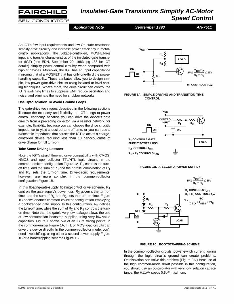
Insulated-Gate Transistors Simplify AC-MotorSpeed Control
An IGT’s few input requirements and low On-state resistancesimplify drive circuitry and increase power efficiency in motor-control applications. The voltage-controlled, MOSFET-likeinput and transfer characteristics of the insulated-gate transis-tor (IGT) (see EDN, September 29, 1983, pg 153 for IGTdetails) simplify power-control circuitry when compared withbipolar devices. Moreover, the IGT has an input capacitancemirroring that of a MOSFET that has only one-third the power-handling capability. These attributes allow you to design sim-ple, low-power gate-drive circuits using isolated or level-shift-ing techniques. What’s more, the drive circuit can control theIGT’s switching times to suppress EMI, reduce oscillation andnoise, and eliminate the need for snubber networks.
Use Optoisolation To Avoid Ground Loops
The gate-drive techniques described in the following sectionsillustrate the economy and flexibility the IGT brings to powercontrol: economy, because you can drive the device’s gatedirectly from a preceding collector, via a resistor network, forexample; flexibility, because you can choose the drive circuit’simpedance to yield a desired turn-off time, or you can use aswitchable impedance that causes the IGT to act as a charge-controlled device requiring less than 10 nanocoulombs ofdrive charge for full turn-on.
Take Some Driving Lessons
Note the IGT’s straightforward drive compatibility with CMOS,NMOS and open-collector TTL/HTL logic circuits in thecommon-emitter configuration Figure 1A. R3 controls the turn-off time, and the sum of R3 and the parallel combination of R1and R2 sets the turn-on time. Drive-circuit requirements,however, are more complex in the common-collectorconfiguration Figure 1B.
In this floating-gate-supply floating-control drive scheme, R1controls the gate supply’s power loss, R2 governs the turn-offtime, and the sum of R1 and R2 sets the turn-on time. Figure1C shows another common-collector configuration employinga bootstrapped gate supply. In this configuration, R3 definesthe turn-off time, while the sum of R2 and R3 controls the turn-on time. Note that the gate’s very low leakage allows the useof low-consumption bootstrap supplies using very low-valuecapacitors. Figure 1 shows two of an IGT’s strong points. Inthe common-emitter Figure 1A, TTL or MOS-logic circuits candrive the device directly. In the common-collector mode, you’llneed level shifting, using either a second power supply Figure1B or a bootstrapping scheme Figure 1C.
In the common-collector circuits, power-switch current flowingthrough the logic circuit’s ground can create problems.Optoisolation can solve this problem (Figure 2A.) Because ofthe high common-mode dV/dt possible in this configuration,you should use an optoisolator with very low isolation capaci-tance; the H11AV specs 0.5pF maximum.
FIGURE 1A. SIMPLE DRIVING AND TRANSITION-TIMECONTROL
FIGURE 1B. A SECOND POWER SUPPLY
FIGURE 1C. BOOTSTRAPPING SCHEME
LOAD
VCC
R1
R3
R2
ON
OFF 15VCCR2R1 R2+-------------------- 25V≤ ≤
R3 CONTROLS tOFF
LOAD
VCC
CONTROLINPUT
ON
OFF 15V
R1 R2
R1 CONTROLS GATESUPPLY POWER LOSS
R2 CONTROLS tOFF
R1 + R2 CONTROLS tON
LOAD
ON
OFF
15VCCR2R1 R2+-------------------- 25V≤ ≤
R3 CONTROLS tOFFR2 + R3 CONTROLS tON
τ 5CICEO IGES 2IR+ +-------------------------------------------------«R1
R3R2
Application Note September 1993 AN-7511
/Title AN751)Sub-ect InulatedGate ranistors im-lify C-otor
peed on-
rol)Autho ()Key-ords
Inter-il orpo-
ation,emi-on-uctor, va-
anche nergy ated, witch
ng ower up-lie, ower

©2002 Fairchild Semiconductor Corporation Application Note 7511 Rev. A1
For optically isolated “relay-action” switching, it makes senseto replace the phototransistor optocoupler with an H11L1Schmitt-trigger optocoupler (Figure 2B).) For applicationsrequiring extremely high isolation, you can use an optical fiberto provide the signal to the gate-control photodetector. Thesecircuit examples use a gate-discharge resistor to control theIGT’s turn-off time. To exploit fully the IGT’s safe operatingarea (SOA), this resistor allows time for the device’s minoritycarriers to recombine. Furthermore, the recombination occurswithout any current crowding that could cause hot-spot forma-tion or latch-up pnpn action. For very fast turn-off, you can usea minimal snubber network, which allows the safe use of lowervalue gate resistors and higher collector currents.
Pulse-Transformer Drive Is Cheap And Efficient
Photovoltaic couplers provide yet another means of driving theIGT. Typically, these devices contain an array of small siliconphotovoltaic cells, illuminated by an infrared diode through atransparent dielectric. The photovoltaic coupler provides anisolated, controlled, remote dc supply without the need foroscillators, rectifiers or filters. What’s more, you can drive it
directly from TTL levels, thanks to its 1.2V, 20mA inputparameters.
Available photovoltaic couplers have an output-currentcapability of approximately 100µA. Combined withapproximately 100kΩ equivalent shunt impedance and theIGT’s input capacitance, this current level yields very longswitching times. These transition times (typically ranging to 1msec) vary with the photovoltaic coupler’s drive current and theIGT’s Miller-effect equivalent capacitance.
Figure 3 illustrates a typical photovoltaic-coupler drive alongwith its transient response. In some applications, thephotovoltaic element can charge a storage capacitor that’ssubsequently switched with a phototransistor isolator. Thisisolator technique - similar to that used in bootstrap circuitsprovides rapid turn-on and turn-off while maintaining small size,good isolation and low cost.
In common-collector applications involving high-voltage, reac-tive-load switching, capacitive currents in the low-level logic cir-cuits can flow through the isolation capacitance of the controlelement (eg, a pulse transformer, optoisolator, piezoelectriccoupler or level-shift transistor). These currents can causeundesirable effects in the logic circuitry, especially in high-impedance, low-signal-level CMOS circuits.
FIGURE 3. AS ANOTHER OPTICAL-DRIVE OPTION, A PHOTO-VOLTAIC COUPLER PROVIDES AN ISOLATED,REMOTE DC SUPPIY TO THE IGT’S INPUT. ITSLOW 100µA OUTPUT, HOWEVER, YIELDS LONGIGT TURN-ON AND TURN-OFF TIMES.
The solution? Use fiber-optic components Figure 4 to elimi-nate the problems completely. As an added feature, this low-cost technique provides physical separation between thepower and logic circuitry, thereby eliminating the effects ofradiated EMI and high-flux magnetic fields typically foundnear power-switching circuits. You could use this methodwith a bootstrap-supply circuit, although the fiber-optic sys-tem’s reduced transmission efficiency could require again/speed trade-off. The added bipolar signal transistorminimizes the potential for compromise.
FIGURE 2A. AVOID GROUND-LOOP PROBLEMS BY USING AN OPTOISOLATOR. THE ISOLATOR IGNORES SYS-TEM GROUND CURRENTS AND ALSO PRO-VIDES HIGH COMMON-MODE RANGE.
FIGURE 2B. A SCHMITT-TRIGGER OPTOISOLATOR YIELDS “SNAP-ACTION” TRIGGERING SIMILAR TOTHAT OF A RELAY.
LOAD
VCC
R1
R2 R3
CONTROLINPUT
C
OFF
ON
H11AV2
LOAD
VCC = 300V
43k
1N5061
5.6k10µF35VCONTROL
INPUTOFF
ON
H11L1
5.6k 5.6k
DIG22 IGTON
OFF
CONTROLINPUT
+
-
I
OUTPUTCURRENT
INPUTCURRENT 0 1 2ms
Application Note 7511

©2002 Fairchild Semiconductor Corporation Application Note 7511 Rev. A1
FIGURE 5A. YIELDING 4-kV ISOLATION, A PIEZOELECTRIC COUPLER PROVIDES TRANSFORMER-LIKE PERFORMANCE AND AN ISOLATED POWER SUPPLY.
FIGURE 5B. THIS CIRCUIT PROVIDES THE DRIVE FOR THIS ARTICLE’S MOTOR-CONTROL CIRCUIT.
CONTROLINPUT
ON
OFF
GFOE1A1
EMITTER(DISCONNECTED)
DETECTOR(CONNECTED)
10M (30FT)QSF2000C
(W/CONNECTORS)
GFOD1A1
1N914
R1
2N5354
CQ1
R2 R3IGT
+
-
FIGURE 4. ELIMINATE EMI IN HIGH-FLUX OR NOISE ENVI-RONMENTS BY USING FIBER-OPTIC COMPO-NENTS. THESE PARTS ALSO ALLEVIATEPROBLEMS ARISING FROM CAPACITIVE COU-PLING IN ISOLATION ELEMENTS.
Piezos Pare Prices
OUTPUTVOLTAGE
ACOUSTIC WAVE
OSCILLATOR
IGT
4.7k
1N914
1N914
PZ61343
D33D21
18V2.5k
3.3k
2.7k
0.001µF
0.001µF
1kNE555
Application Note 7511

©2002 Fairchild Semiconductor Corporation Application Note 7511 Rev. A1
A piezoelectric coupler operationally similar to a pulse-traindrive transformer, but potentially less costly in high volume isa small, efficient device with isolation capability ranging to4kV. What’s more, unlike optocouplers, they require noauxiliary power supply. The piezo element is a ceramiccomponent in which electrical energy is converted tomechanical energy, transmitted as an acoustic wave, andthen reconverted to electrical energy at the output terminalsFigure 5A.
The piezo element’s maximum coupling efficiency occurs atits resonant frequency, so the control oscillator must operateat that frequency. For example, the PZT61343 piezo couplerin Figure 5B’s driver circuit requires a 108kHz, ±1%-accurateastable multivibrator to maximize mechanical oscillations inthe ceramic material. This piezo element has a 1W maxpower handling capability and a 30mA p-p max secondarycurrent rating. The 555 timer shown provides compatiblewaveforms while the RC network sets the frequency.
Isolate With Galvanic Impunity
Do you require tried and true isolation? Then usetransformers; the IGT’s low gate requirements simplify thedesign of independent, transformer-coupled gate-drivesupplies. The supplies can directly drive the gate and itsdischarge resistor Figure 6, or they can simply replace thelevel-shifting supplies of Figure 2. It’s good practice to usepulse transformers in drive circuitry, both for IGT’s andMOSFETs, because these components are economical,rugged and highly reliable.
FIGURE 6A. PROVIDING HIGH ISOLATION AT LOW COST, PULSE TRANSFORMERS ARE IDEAL FOR DRIVING THEIGT. AT SUFFICIENTLY HIGH FREQUENCIES, C1CAN BE THE IGT’S GATE-EMITTER CAPACITANCEALONE.
FIGURE 6B. A HIGH-FREQUENCY OSCILLATOR IN THE TRANS-FORMER’S PRIMARY YIELDS UNLIMITED ON-TIME CAPABILITY.
In the pulse-on, pulse-off method Figure 6A, C1 stores apositive pulse, holding the IGT on. At moderate frequencies(several hundred Hertz and above), the gate-emittercapacitance alone can store enough energy to keep the IGTon; lower frequencies require an additional external capacitor.Use of the common-base n-p-n bipolar transistor to dischargethe capacitance minimizes circuit loading on the capacitor.This action extends continuous on-time capability withoutcapacitor refreshing; it also controls the gate-discharge timevia the 1kΩ emitter resistor.
FIGURE 8. THIS 6-STEP 3-PHASE-MOTOR DRIVE USES THE IGT-DRIVE TECHNIQUES DESCRIBED IN THE TEXT. THE REGULATOR AD-JUSTS THE OUTPUT DEVICES’ INPUT LEVELS; THE VOLTAGE-CONTROLLED OSCILLATOR VARIES THE SWITCHINGFREQUENCY AND ALSO PROVIDES THE CLOCK FOR THE 3-PHASE TIMING LOGIC. THE V/F RATIO STAYS CONSTANTTO MAINTAIN CONSTANT TORQUE REGARDLESS OF SPEED.
ON
OFF
CONTROLINPUT
1N914
1N914
2N5232
PULSETRANSFORMER
1k
C1IGT
+
-
IGT
+
-
ON OFF 1N914
CONTROLINPUT
1N914 RC = 3µSEC
C R
CURRENTSENSESIGNAL
ENABLELOWER
LEGS
SHUT DOWNDRIVEOSCILLATOR
VARIABLEDC VOLTAGE
TIMING
AND DRIVEVOLTAGEENABLE
ADJUST VOLTAGE
5V
24V
24V DC
220V AC3φ 60Hz THREE-PHASE
BRIDGERECTIFIER
LOW VOLTAGETRANSFORMER
RECTIFIERFILTER
SWITCHINGREGULATOR
POWER SUPPLYFOR CONTROL
CIRCUITS
VOLTAGECONTROLLED
OSCILATOR
MOTORCONTROL
LOGIC
OVERLOADPROTECTION
THREE-PHASEIGT
INVERTER
TACHO-METER
FEEDBACK
SIGNAL PATH ISOLATOREG: OPTOCOUPLIER PIEZO COUPLER
3φINDUCTION
MOTOR
I I I
I
I
Application Note 7511

©2002 Fairchild Semiconductor Corporation Application Note 7511 Rev. A1
Piezoelectric Couplers Provide 4-kV Isolation
Using a high-frequency oscillator for pulse-train drive Figure6B yields unlimited on-time capability. However, the schemerequires an oscillator that can be turned on and off by thecontrol logic. A diode or zener clamp across the trans-former’s primary will limit leakage-inductance flyback effects.To optimize transformer efficiency, make the pulses’ voltagex time products equal for both the On and the Off pulses. Insituations where the line voltage generates the drive power,a simple relaxation oscillator using a programmable unijunc-tion transistor can derive its power directly from the line toprovide a pulse train to the IGT gate.
The circuit shown in Figure 7 accommodates applicationsinvolving lower frequencies (a few hundred Hertz andbelow). The high oscillator frequency (greater than 20kHz)helps keep the pulse transformer reasonably small. The volt-
age-doubler circuitry improves the turn-on time and also pro-vides long on-time capability. Although this design uses onlya 5V supply on the primary side of a standard trigger trans-former, it provides 15V gate-to-emitter voltage.
FIGURE 7. THIS DRIVING METHOD FOR LOW-FREQUENCY SWITCHING PROVIDES 15V TO THE IGT’S GATE
OSCILLATOR1:2
1N914
0.001µF
4.7k
0.001µF IGT
1N914
FIGURE 9A. THE POWER INVERTER’S DRIVE CIRCUIT USES SIX IGTS TO DRIVE A 2-HP MOTOR.
FIGURE 9B. THE TIMING DIAGRAM SHOWS THAT EACH IGT CONDUCTS FOR 165o× OF EVERY 360o CYCLE;THE DELAY IS NECESSARY TO AVOID CROSSCONDUCTION.
FIGURE 9C. THE THREE WINDINGS’ VOLTAGES AND CUR-RENTS ARE SHOWN. NOTE THAT ALTHOUGHCOSTLY SNUBBER NETWORKS ARE ELIMINAT-ED, FREEWHEELING DIODES ARE NEEDED; THEIGTS HAVE NO INTRINSIC OUTPUT DIODE.
INDUCTIONMOTOR
D7
325V10A
NOTES:Q1 - Q6 = D94FR4D1 - D7 = 1N3913D8 - D13 = 1N914
R = 4.7k, 1/2WC1 = 100µF, 400VL1 = 40µH
220V
L1
D1
D2
Q2
Q1R
R
C1
D3 D5
Q3 Q5R R
RR Q4 Q6
D4 D6
t
t
t
t
t
t0
0
0
0
0
0
φA
φB
φC
ILA
ILB
ILC
Q1 ON
Q2ON
Q3ON
180o
15o DELAY
Q4ON
Q5ONQ6ON
VAB0 t
VBC
VCA
ILA
ILB
ILC
0
0
0
0
0
t
t
t
t
t
Application Note 7511
©2002 Fairchild Semiconductor Corporation Application Note 7511 Rev. A1
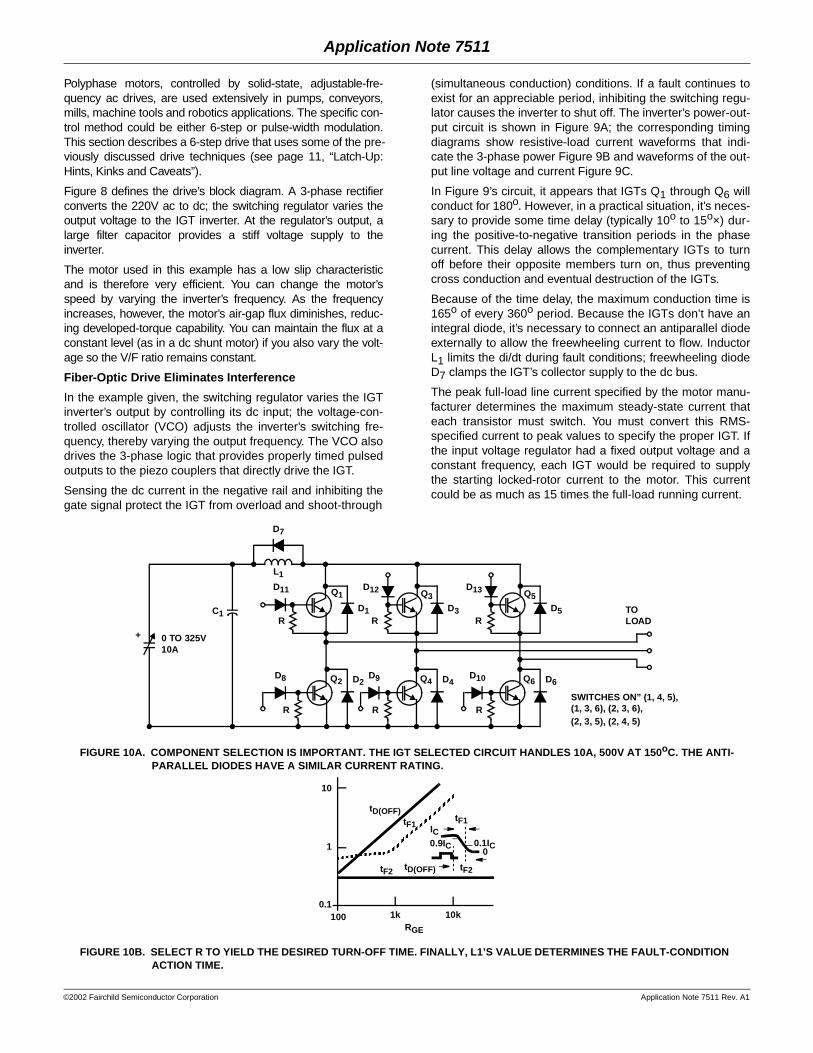
Polyphase motors, controlled by solid-state, adjustable-fre-quency ac drives, are used extensively in pumps, conveyors,mills, machine tools and robotics applications. The specific con-trol method could be either 6-step or pulse-width modulation.This section describes a 6-step drive that uses some of the pre-viously discussed drive techniques (see page 11, “Latch-Up:Hints, Kinks and Caveats”).
Figure 8 defines the drive’s block diagram. A 3-phase rectifierconverts the 220V ac to dc; the switching regulator varies theoutput voltage to the IGT inverter. At the regulator’s output, alarge filter capacitor provides a stiff voltage supply to theinverter.
The motor used in this example has a low slip characteristicand is therefore very efficient. You can change the motor’sspeed by varying the inverter’s frequency. As the frequencyincreases, however, the motor’s air-gap flux diminishes, reduc-ing developed-torque capability. You can maintain the flux at aconstant level (as in a dc shunt motor) if you also vary the volt-age so the V/F ratio remains constant.
Fiber-Optic Drive Eliminates Interference
In the example given, the switching regulator varies the IGTinverter’s output by controlling its dc input; the voltage-con-trolled oscillator (VCO) adjusts the inverter’s switching fre-quency, thereby varying the output frequency. The VCO alsodrives the 3-phase logic that provides properly timed pulsedoutputs to the piezo couplers that directly drive the IGT.
Sensing the dc current in the negative rail and inhibiting thegate signal protect the IGT from overload and shoot-through
(simultaneous conduction) conditions. If a fault continues toexist for an appreciable period, inhibiting the switching regu-lator causes the inverter to shut off. The inverter’s power-out-put circuit is shown in Figure 9A; the corresponding timingdiagrams show resistive-load current waveforms that indi-cate the 3-phase power Figure 9B and waveforms of the out-put line voltage and current Figure 9C.
In Figure 9’s circuit, it appears that IGTs Q1 through Q6 willconduct for 180o. However, in a practical situation, it’s neces-sary to provide some time delay (typically 10o to 15o×) dur-ing the positive-to-negative transition periods in the phasecurrent. This delay allows the complementary IGTs to turnoff before their opposite members turn on, thus preventingcross conduction and eventual destruction of the IGTs.
Because of the time delay, the maximum conduction time is165o of every 360o period. Because the IGTs don’t have anintegral diode, it’s necessary to connect an antiparallel diodeexternally to allow the freewheeling current to flow. InductorL1 limits the di/dt during fault conditions; freewheeling diodeD7 clamps the IGT’s collector supply to the dc bus.
The peak full-load line current specified by the motor manu-facturer determines the maximum steady-state current thateach transistor must switch. You must convert this RMS-specified current to peak values to specify the proper IGT. Ifthe input voltage regulator had a fixed output voltage and aconstant frequency, each IGT would be required to supplythe starting locked-rotor current to the motor. This currentcould be as much as 15 times the full-load running current.
FIGURE 10A. COMPONENT SELECTION IS IMPORTANT. THE IGT SELECTED CIRCUIT HANDLES 10A, 500V AT 150oC. THE ANTI-PARALLEL DIODES HAVE A SIMILAR CURRENT RATING.
FIGURE 10B. SELECT R TO YIELD THE DESIRED TURN-OFF TIME. FINALLY, L1’S VALUE DETERMINES THE FAULT-CONDITION ACTION TIME.
D7
0 TO 325V10A
SWITCHES ON” (1, 4, 5),(1, 3, 6), (2, 3, 6),(2, 3, 5), (2, 4, 5)
L1
D1
Q1
RC1
D5
Q5
R
R
Q6 D6
TOLOAD
D13
D10
R
Q4 D4D9
R
Q2 D2D8
D3
Q3
R
D12D11
+
10
1
0.1100 1k 10k
RGE
tD(OFF)tF1
tF2 tF2
tF1
tD(OFF)
IC0.9IC 0.1IC
0
Application Note 7511
©2002 Fairchild Semiconductor Corporation Application Note 7511 Rev. A1
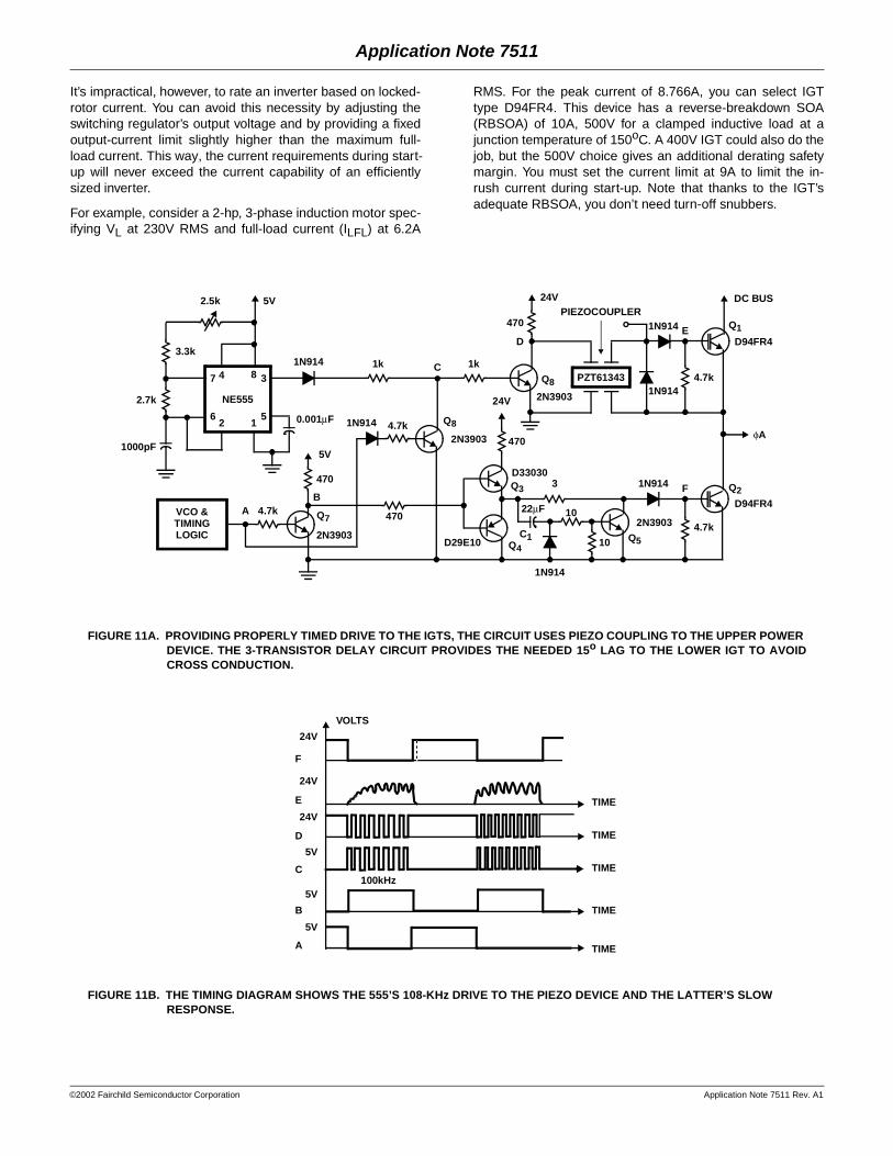
It’s impractical, however, to rate an inverter based on locked-rotor current. You can avoid this necessity by adjusting theswitching regulator’s output voltage and by providing a fixedoutput-current limit slightly higher than the maximum full-load current. This way, the current requirements during start-up will never exceed the current capability of an efficientlysized inverter.
For example, consider a 2-hp, 3-phase induction motor spec-ifying VL at 230V RMS and full-load current (ILFL) at 6.2A
RMS. For the peak current of 8.766A, you can select IGTtype D94FR4. This device has a reverse-breakdown SOA(RBSOA) of 10A, 500V for a clamped inductive load at ajunction temperature of 150oC. A 400V IGT could also do thejob, but the 500V choice gives an additional derating safetymargin. You must set the current limit at 9A to limit the in-rush current during start-up. Note that thanks to the IGT’sadequate RBSOA, you don’t need turn-off snubbers.
FIGURE 11A. PROVIDING PROPERLY TIMED DRIVE TO THE IGTS, THE CIRCUIT USES PIEZO COUPLING TO THE UPPER POWER DEVICE. THE 3-TRANSISTOR DELAY CIRCUIT PROVIDES THE NEEDED 15o LAG TO THE LOWER IGT TO AVOIDCROSS CONDUCTION.
FIGURE 11B. THE TIMING DIAGRAM SHOWS THE 555’S 108-KHz DRIVE TO THE PIEZO DEVICE AND THE LATTER’S SLOWRESPONSE.
1N914
NE555
47 8 3
2 156
2N3903
VCO &TIMINGLOGIC
1000pF
2.7k
3.3k1k
5V
0.001µF
5V
A 4.7k
470
Q7
B
1N914 4.7k
C
Q8
2N3903
2N3903
Q8
470
470
1N914
1N914
2N3903
1N914D33030
D29E10
1N914
D94FR4
D94FR4
PIEZOCOUPLER
24V
24V
Q3
Q4Q5
Q1
Q2
4.7k
4.7k10
10
22µF
C1
DC BUS
φA
E
F
D
3
PZT613431k
470
2.5k
VOLTS
24V
F
24V
E
24V
D
C
B
A
TIME
TIME
TIME
TIME
TIME
5V
5V
5V
100kHz
Application Note 7511
©2002 Fairchild Semiconductor Corporation Application Note 7511 Rev. A1
Use 6-Step Drive For Speed-Invariant Torque
Figure 10A shows the inverter circuit configured for thisexample. Diodes D1 through D6 carry the same peak currentas the IGTs; consequently, they’re rated to handle peak cur-rents of at least 8.766A. However, they only conduct for ashort time (15o to 20o of 180o), so their average-currentrequirement is relatively small.
External circuitry can control the IGT’s current fall time.Resistor R controls tF1 Figure 10B; there's no way to controltF2, an inherent characteristic of the selected IGT. In thisexample, a 4.7-kΩ gate-to-emitter resistor provides theappropriate fall time. The choice of current-limiting inductorL1 is based on the IGT’s overload-current rating and theaction time (the sum of the sensor’s sensing and responsetime and the IGT’s turn-off time) in fault conditions.
You could use a set of flip flops and a multivibrator to gener-ate the necessary drive pulses and the corresponding 120o×delay between the three phases in Figure 10’s circuit. A volt-age-controlled oscillator serves to change the inverter’s out-put frequency. In this circuit, IGTs Q1, Q3 and Q5 requireisolated gate drive; the drive for Q2, Q4 and Q6 can bereferred to common. If you use optocouplers for isolation,you’ll need three isolated or bootstrap power supplies (inaddition to the 5V and 24V power supplies) to drive the IGTs.Another alternative is to use transformer coupling.
165o Conduction Prevents Shoot-Through
Consider, however, using Figure 11A’s novel, low-cost cir-cuit. It uses a piezo coupler to drive the isolated IGT. Asnoted, the coupler needs a high-frequency square wave toinduce mechanical oscillations in its primary side. The 555oscillator provides the necessary 108-kHz waveform; its out-put is gated according to the required timing logic and thenapplied to the piezo coupler’s primary. The coupler’s rectifiedoutput drives the IGT’s gate; the 4.7kW gate-to-emitter resis-tor provides a discharge path for CGE during the IGT’s turn-off. The circuit’s logic-timing diagram is shown in Figure 11B.
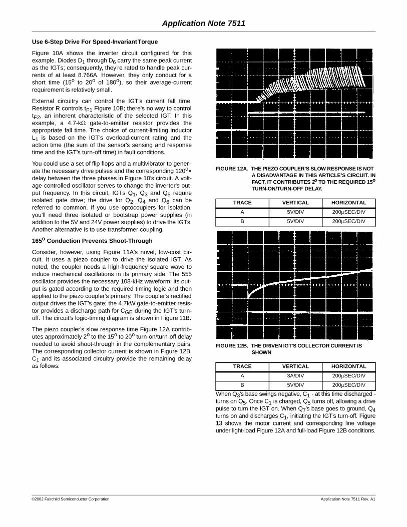
The piezo coupler’s slow response time Figure 12A contrib-utes approximately 2o to the 15o to 20o turn-on/turn-off delayneeded to avoid shoot-through in the complementary pairs.The corresponding collector current is shown in Figure 12B.C1 and its associated circuitry provide the remaining delayas follows:
FIGURE 12A. THE PIEZO COUPLER’S SLOW RESPONSE IS NOT A DISADVANTAGE IN THIS ARTICLE’S CIRCUIT. INFACT, IT CONTRIBUTES 2o TO THE REQUIRED 15o
TURN-ON/TURN-OFF DELAY.
FIGURE 12B. THE DRIVEN IGT'S COLLECTOR CURRENT IS SHOWN
When Q3’s base swings negative, C1 - at this time discharged -turns on Q5. Once C1 is charged, Q5 turns off, allowing a drivepulse to turn the IGT on. When Q7’s base goes to ground, Q4turns on and discharges C1, initiating the IGT’s turn-off. Figure13 shows the motor current and corresponding line voltageunder light-load Figure 12A and full-load Figure 12B conditions.
TRACE VERTICAL HORIZONTAL
A 5V/DIV 200µSEC/DIV
B 5V/DIV 200µSEC/DIV
TRACE VERTICAL HORIZONTAL
A 3A/DIV 200µSEC/DIV
B 5V/DIV 200µSEC/DIV
Application Note 7511

©2002 Fairchild Semiconductor Corporation Application Note 7511 Rev. A1
.
FIGURE 13A. MOTOR CURRENT AND VOLTAGE ARE SHOWN HERE, FOR LIGHT LOADS
FIGURE 13B. MOTOR CURRENT AND VOLTAGE ARE SHOWN HERE, FOR HEAVY LOADS.
To complete the design of the 6-step motor drive, it’s necessary to consider protection circuitry for the output IGTs. The drive receives itspower from a switching supply already containing provisions for protection from line over-voltage and under-voltage and transient effects.However, you still have to guard the power switches against unwanted effects on the output lines and the possibility of noise or otherextraneous signals causing gate-drive timing errors.
The best protection circuit must match the characteristics of the power switch and the circuit’s bias conditions. The IGT is very ruggedduring turn-on and conduction, but it requires time to dissipate minority carriers when turning off high currents and voltages. An analysisof the possible malfunction condition
FIGURE 14. THE LOWEST COST SENSOR IMAGINABLE, A PIECE OF COPPER WIRE SERVES AS THE CURRENT MONITOR IN THIS SYS-TEM. THE CHOPPED AND AMPLIFIED VOLTAGE DROP ACROSS THE WIRE TRIGGERS A GATE-DRIVE SHUT-OFF CIRCUITUNDER FAULT CONDITIONS.
TRACE VERTICAL HORIZONTAL
A 1A/DIV 1mSEC/DIV
B 50V/DIV 1mSEC/DIV
TRACE VERTICAL HORIZONTAL
A 3A/DIV 2mSEC/DIV
B 100V/DIV 2mSEC/DIV
ACLINE
INPUT
HVDISABLE
GATE DRIVE TURNOFF
HVADJUST
50 TO 320V DC
5V DCUPPER 3
LOWER 3
dI/dt LIMIT24V DC
CHOPPER
I LIMIT
10A
20A
ISOLATIONISOLATION
IGTSWITCHES MOTOR
CONTROLAND
TIMING
ISOLATION
RECTIFIERAND
FILTER
SWITCHINGPOWERSUPPLY
RECYCLETIME
COMPARATORAND LATCH
ACAV = 100
ISOLATION
Application Note 7511

©2002 Fairchild Semiconductor Corporation Application Note 7511 Rev. A1
FIGURE 15A. THIS ALL-ENCOMPASSING PROTECTION SYSTEM PROVIDES THREE INDEPENDENT SHUTDOWN FUNCTONS - ONE EACH FOR THE UPPER AND LOWER IGTS AND THE HIGH-VOLTAGE SUPPLY.
FIGURE 15B. THIS CIRCUIT PROVIDES CHOPPER DRIVE FOR THE COPPER-WIRE SENSOR IN FIGURE 15A.
FIGURE 15C. SHOWS THE HIGH-VOLT-AGE SHUTDOWN CIRCUIT.
50 TO 320V DC
24V
3.9k
750k3.3k
2.7k
2N5355
470pF
0.01µF10A
2k
5µF20V
150
2N5232
15V
5µF25V
220k2.2k
0.001µF
H11F3
H11F3 TOCONTROL CIRCUIT
39
470pF
39020A2k
2mΩ (1” #24 AWG COPPER)
POWERSUPPLY
CURRENTSENSE ANDCHOPPER
ACAMPLIFIER
LATCHINGFAST
COMPARATOR
10msRESET
IGT POWER SWITCHES
A139M
50µH
10k
180k47k
39k
0.001µF
1k
2N5306
C203B
0.02µF
22k
H11AV2 TO PZO SHUTDOWN
H11AV2 TO HI-V SHUTDOWN
22
0.2µF2
1
TODRIVE
DT230F
TOMOTOR
TIMER555
1 3
CHOPPER DRIVE
TO PIEZODRIVERS
5V
150150
180
0.002µF5.1k
2N5232
H11F3H11F3
100
180
0.002µF 5.1k
2N5232
0.005µF
150
DT230F(3)
47k
H11AV2
10µF10V
ALL OPTOCOUPLERS GO TO PROTECTION CIRCUIT
SG3524
1516
10 8
HIGH-VOLTAGE SHUTDOWN
24VTO
CONTROL
5V2.2k
0.005µF
1M
Application Note 7511
©2002 Fairchild Semiconductor Corporation Application Note 7511 Rev. A1
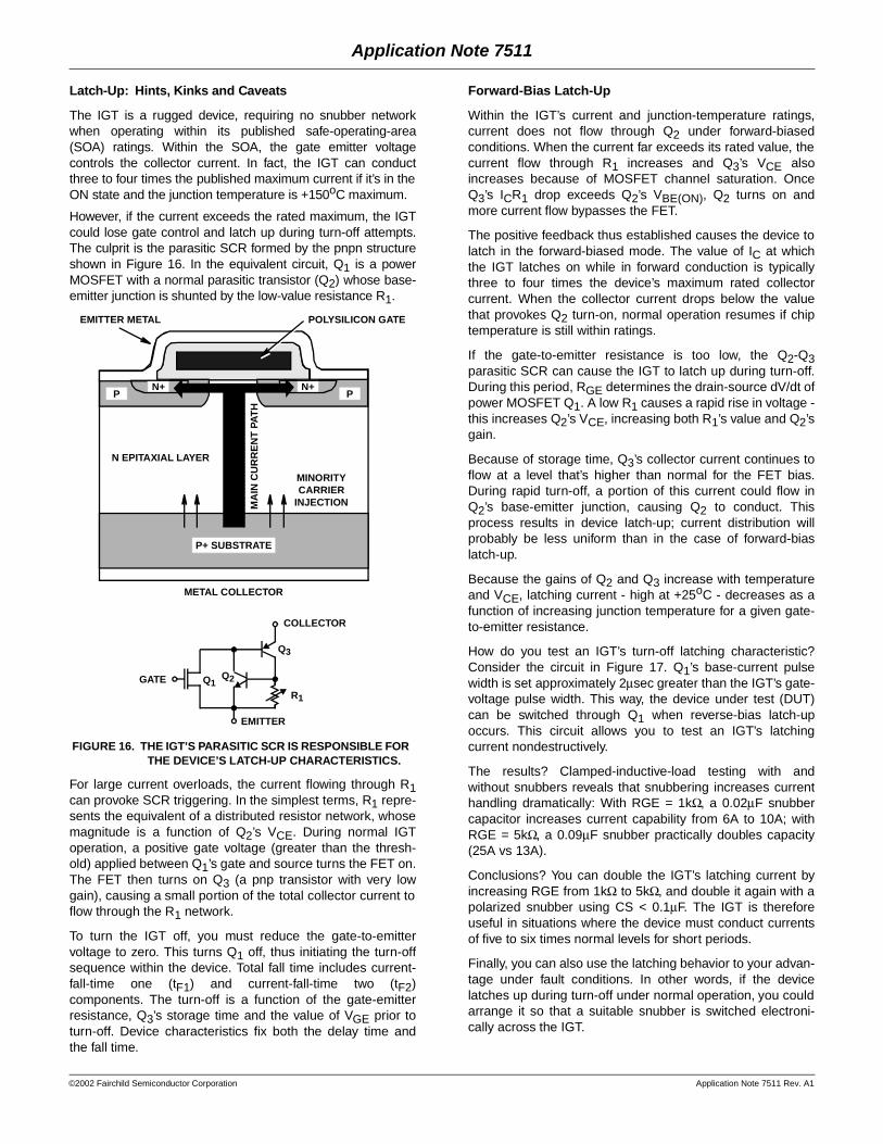
Latch-Up: Hints, Kinks and Caveats
The IGT is a rugged device, requiring no snubber networkwhen operating within its published safe-operating-area(SOA) ratings. Within the SOA, the gate emitter voltagecontrols the collector current. In fact, the IGT can conductthree to four times the published maximum current if it’s in theON state and the junction temperature is +150oC maximum.
However, if the current exceeds the rated maximum, the IGTcould lose gate control and latch up during turn-off attempts.The culprit is the parasitic SCR formed by the pnpn structureshown in Figure 16. In the equivalent circuit, Q1 is a powerMOSFET with a normal parasitic transistor (Q2) whose base-emitter junction is shunted by the low-value resistance R1.
FIGURE 16. THE IGT’S PARASITIC SCR IS RESPONSIBLE FOR THE DEVICE’S LATCH-UP CHARACTERISTICS.
For large current overloads, the current flowing through R1can provoke SCR triggering. In the simplest terms, R1 repre-sents the equivalent of a distributed resistor network, whosemagnitude is a function of Q2’s VCE. During normal IGToperation, a positive gate voltage (greater than the thresh-old) applied between Q1’s gate and source turns the FET on.The FET then turns on Q3 (a pnp transistor with very lowgain), causing a small portion of the total collector current toflow through the R1 network.
To turn the IGT off, you must reduce the gate-to-emittervoltage to zero. This turns Q1 off, thus initiating the turn-offsequence within the device. Total fall time includes current-fall-time one (tF1) and current-fall-time two (tF2)components. The turn-off is a function of the gate-emitterresistance, Q3’s storage time and the value of VGE prior toturn-off. Device characteristics fix both the delay time andthe fall time.
Forward-Bias Latch-Up
Within the IGT’s current and junction-temperature ratings,current does not flow through Q2 under forward-biasedconditions. When the current far exceeds its rated value, thecurrent flow through R1 increases and Q3’s VCE alsoincreases because of MOSFET channel saturation. OnceQ3’s ICR1 drop exceeds Q2’s VBE(ON), Q2 turns on andmore current flow bypasses the FET.
The positive feedback thus established causes the device tolatch in the forward-biased mode. The value of IC at whichthe IGT latches on while in forward conduction is typicallythree to four times the device’s maximum rated collectorcurrent. When the collector current drops below the valuethat provokes Q2 turn-on, normal operation resumes if chiptemperature is still within ratings.
If the gate-to-emitter resistance is too low, the Q2-Q3parasitic SCR can cause the IGT to latch up during turn-off.During this period, RGE determines the drain-source dV/dt ofpower MOSFET Q1. A low R1 causes a rapid rise in voltage -this increases Q2’s VCE, increasing both R1’s value and Q2’sgain.
Because of storage time, Q3’s collector current continues toflow at a level that’s higher than normal for the FET bias.During rapid turn-off, a portion of this current could flow inQ2’s base-emitter junction, causing Q2 to conduct. Thisprocess results in device latch-up; current distribution willprobably be less uniform than in the case of forward-biaslatch-up.
Because the gains of Q2 and Q3 increase with temperatureand VCE, latching current - high at +25oC - decreases as afunction of increasing junction temperature for a given gate-to-emitter resistance.
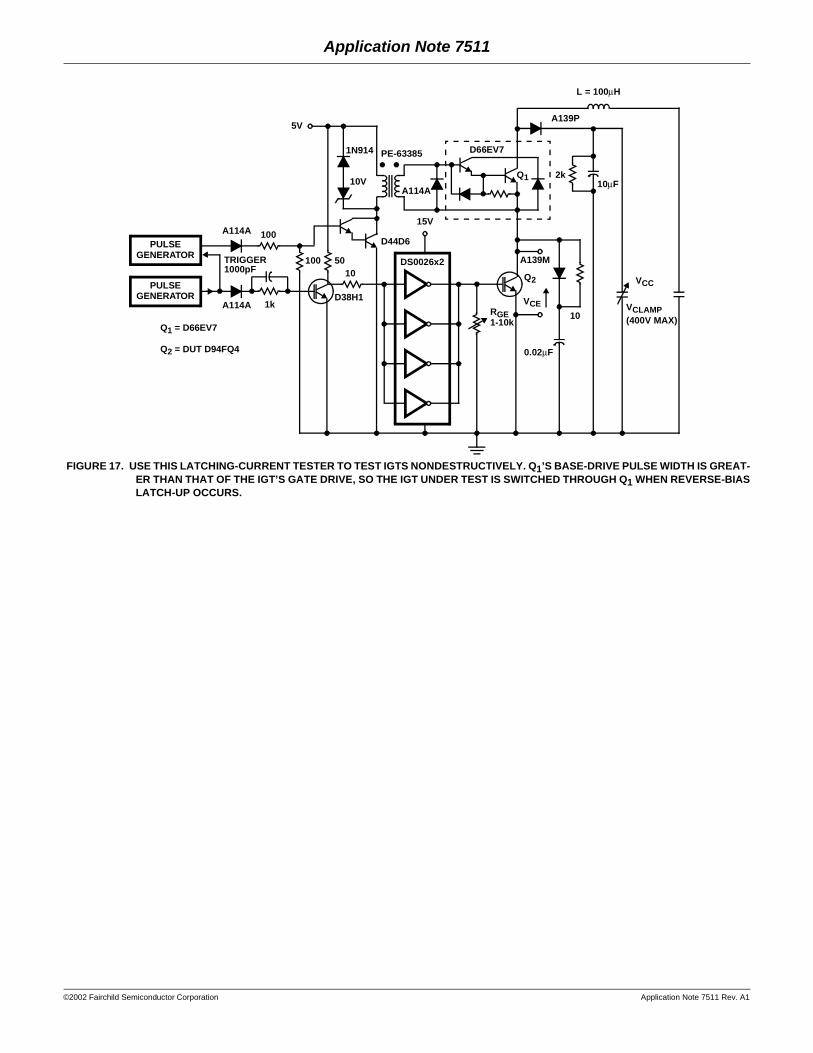
How do you test an IGT’s turn-off latching characteristic?Consider the circuit in Figure 17. Q1’s base-current pulsewidth is set approximately 2µsec greater than the IGT’s gate-voltage pulse width. This way, the device under test (DUT)can be switched through Q1 when reverse-bias latch-upoccurs. This circuit allows you to test an IGT’s latchingcurrent nondestructively.
The results? Clamped-inductive-load testing with andwithout snubbers reveals that snubbering increases currenthandling dramatically: With RGE = 1kΩ, a 0.02µF snubbercapacitor increases current capability from 6A to 10A; withRGE = 5kΩ, a 0.09µF snubber practically doubles capacity(25A vs 13A).
Conclusions? You can double the IGT’s latching current byincreasing RGE from 1kΩ to 5kΩ, and double it again with apolarized snubber using CS < 0.1µF. The IGT is thereforeuseful in situations where the device must conduct currentsof five to six times normal levels for short periods.
Finally, you can also use the latching behavior to your advan-tage under fault conditions. In other words, if the devicelatches up during turn-off under normal operation, you couldarrange it so that a suitable snubber is switched electroni-cally across the IGT.
EMITTER METAL POLYSILICON GATE
P
METAL COLLECTOR
MINORITYCARRIER
INJECTIONMA
IN C
UR
RE
NT
PA
TH
N EPITAXIAL LAYER
P+ SUBSTRATE
N+N+P
COLLECTOR
Q3
R1
EMITTER
GATE Q2Q1
Application Note 7511
©2002 Fairchild Semiconductor Corporation Application Note 7511 Rev. A1
FIGURE 17. USE THIS LATCHING-CURRENT TESTER TO TEST IGTS NONDESTRUCTIVELY. Q1’S BASE-DRIVE PULSE WIDTH IS GREAT-ER THAN THAT OF THE IGT’S GATE DRIVE, SO THE IGT UNDER TEST IS SWITCHED THROUGH Q1 WHEN REVERSE-BIASLATCH-UP OCCURS.
PULSEGENERATOR
PULSEGENERATOR
TRIGGER1000pF
A114A
A114A 1k
100
100
5010
D38H1
D44D6
Q1 = D66EV7
Q2 = DUT D94FQ4
DS0026x2
5V
1N914
10V
PE-63385
A114A
15V
D66EV7
Q1
RGE1-10k
VCE
A139M
10
VCC
VCLAMP(400V MAX)
0.02µF
10µF
A139P
L = 100µH
2k
Q2
Application Note 7511

!"#$%"&'(%& %)'"%&'!%*$%('((!'&$$%"'+'%,'*- %& ''.$'-'($$%+!% !"'*%("&%%$%%( /0!11 2 2345 123 4511 3 45 1 1 1 2 1 3 21 6 2
7 12111 2 1 21 11 23 2
$ 2
((
%
1 1 1122
1 2311 21 2 1
1 2 1
11 2 1 2
"
$
$
($
!" !
#$ !$% $&
'()!!*!* +
,$
" !
% -$"./".0".12 2, "$!$
8$%-'
3%3$45