©Loberg
Introduction to Digital Circuits Basic Logic Circuits
50
10
20 30 40
1 2 3 4 5 6
[ ] AID µ
[ ]VVDS
V0.1VGS −=
V0VGS =
V5.0VGS =
V0.1VGS =
V5.0VGS −=
V5.1VGS −=
Drain characteristic of the load MOSFET Q2
Resistance characteristic of Q2
1Qov
iv
2Q
DDV+
Depletion load
Enhancement driver
0V 2GS =
The NMOS Depletion Load The NMOS Inverter
1
1 2 3 4 5 6
50
100
150
200
250
300
[ ] AID µ
[ ]VVDS
V0.6VGS =
V0.4VGS =
V0.5VGS =
V0.3VGS =
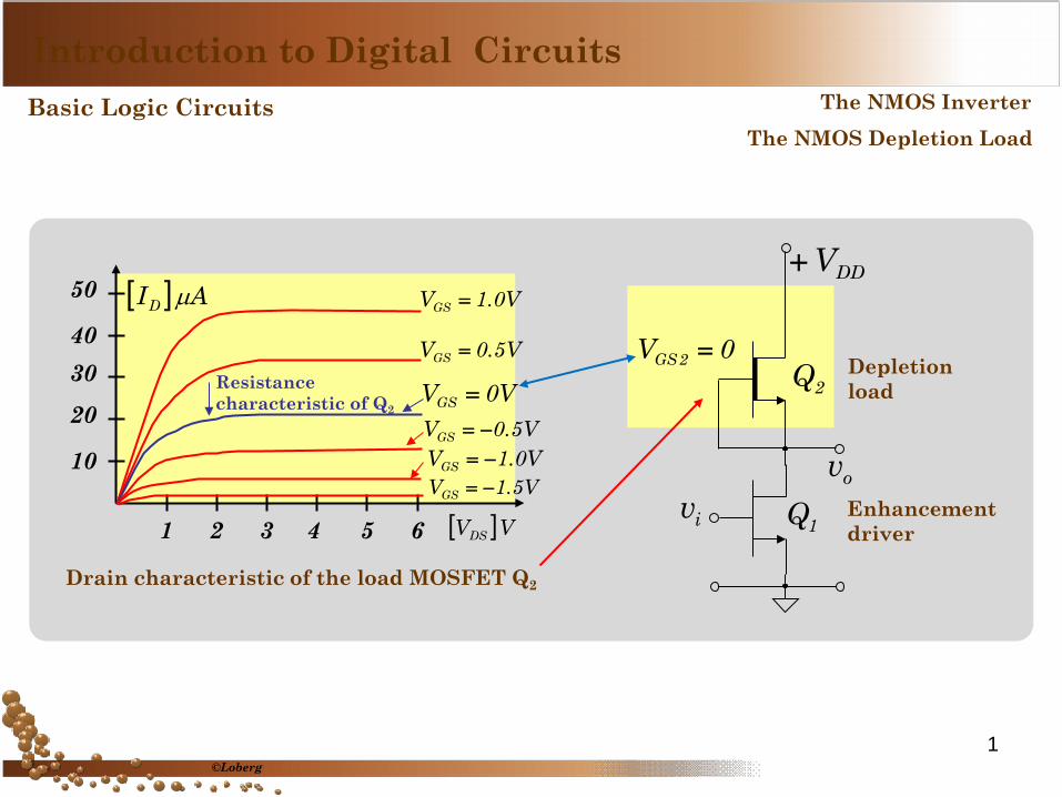
The drain characteristic of the driver MOSFET Q1 . 1DI
Load line
A
B
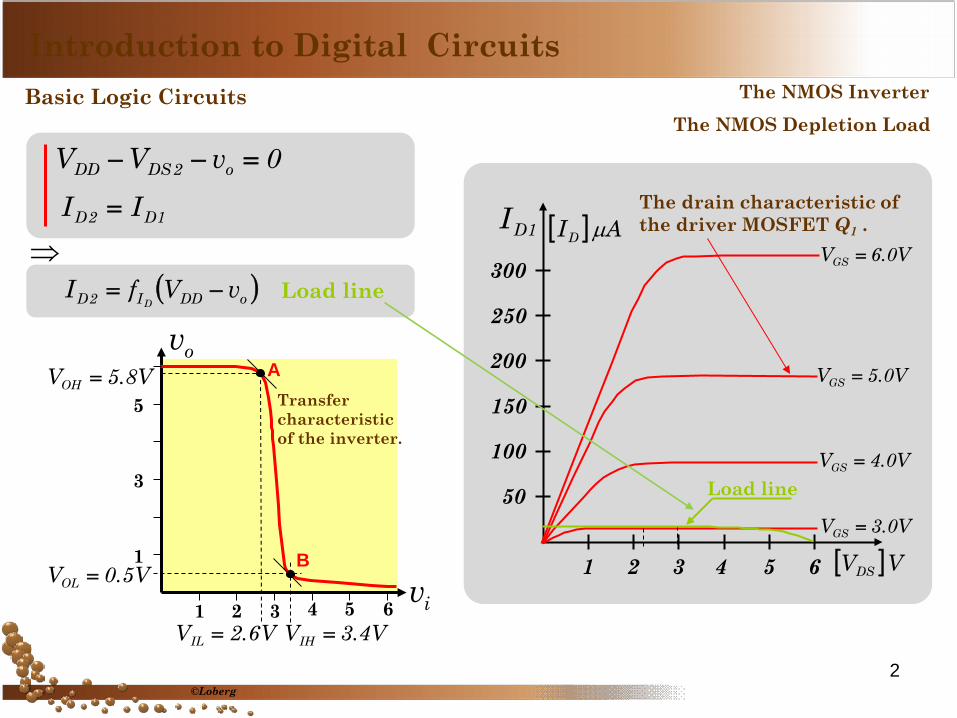
V8.5VOH =
V5.0VOL =
V6.2VIL = V4.3VIH =iv
ov
1 2 3 4 5 6
1
3
5 Transfer characteristic of the inverter.
1D2D II =
0vVV o2DSDD =−−
( )oDDI2D vVfID
−= Load line ⇒
©Loberg
Introduction to Digital Circuits Basic Logic Circuits The NMOS Inverter
The NMOS Depletion Load
2
V1.25.06.2VVNM maxOLmaxILL =−=−=
V4.24.38.5VVNM minIHminOHH =−=−=
V8.5VOH =V5.0VOL =V6.2VIL =V4.3VIH =
⇒ Noise Margins
The additional processing steps are required to fabricate both depletion and enhancement devices on the same chip.
©Loberg
Introduction to Digital Circuits Basic Logic Circuits The NMOS Inverter
The NMOS Depletion Load
3

The Linear (Nonsaturated) Load The Saturated Enhancement Load
iv
ov
1 2 3 4 5 6
1
3
5
Transfer characteristic of the inverter.
Depletion load
Linear load
Saturated load
Saturated load
41
LW
=
41
LW
=
41
LW
=
1LW
=
Summary
©Loberg
Introduction to Digital Circuits Basic Logic Circuits The NMOS Inverter
The NMOS Depletion Load
4
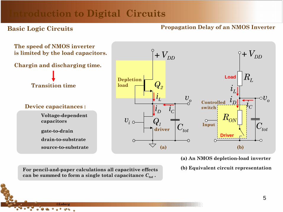
Propagation Delay of an NMOS Inverter
1Q
ov
iv
2Q
DDV+
Depletion load
driver totC
CiLi
Di
totC
Li
DDV+
LR
ONR
DiCi
Driver
Load
ovControlled switch
Input
(a) (b)
(a) An NMOS depletion-load inverter
(b) Equivalent circuit representation
The speed of NMOS inverter is limited by the load capacitors.
Chargin and discharging time.
Transition time
Device capacitances :
gate-to-drain drain-to-substrate source-to-substrate
Voltage-dependent capacitors
For pencil-and-paper calculations all capacitive effects can be summed to form a single total capacitance Ctot .
©Loberg
Introduction to Digital Circuits Basic Logic Circuits
5
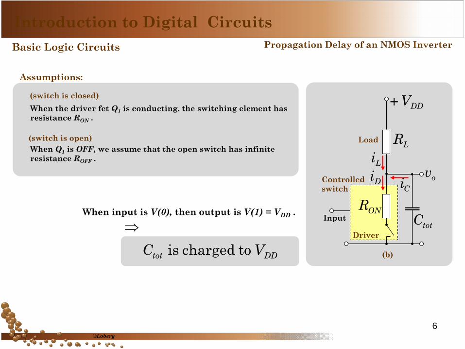
totC
Li
DDV+
LR
ONR
DiCi
Driver
Load
ovControlled switch
Input
(b)
Assumptions:
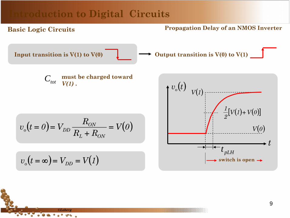
When input is V(0), then output is V(1) = VDD . ⇒
DDtot VC tochargedis
When the driver fet Q1 is conducting, the switching element has resistance RON .
When Q1 is OFF, we assume that the open switch has infinite resistance ROFF .
(switch is closed)
(switch is open)
©Loberg
Introduction to Digital Circuits Basic Logic Circuits Propagation Delay of an NMOS Inverter
6
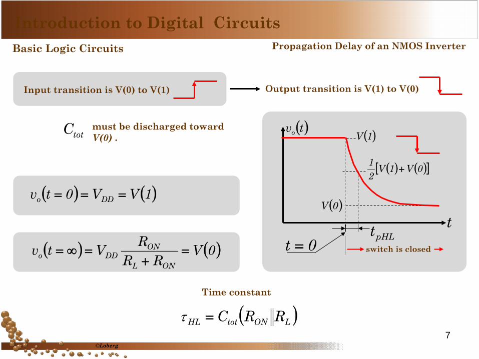
totC must be discharged toward V(0) .
( ) ( )0VRR
RVtvONL
ONDDo =
+=∞=
Time constant
( )LONtotHL RRC=τ
Output transition is V(1) to V(0) Input transition is V(0) to V(1)
( ) ( )1VV0tv DDo ===( )0V
( )1V( )tvo
tpHLt
( ) ( )[ ]0V1V21
+
switch is closed 0t =
©Loberg
Introduction to Digital Circuits Basic Logic Circuits Propagation Delay of an NMOS Inverter
7
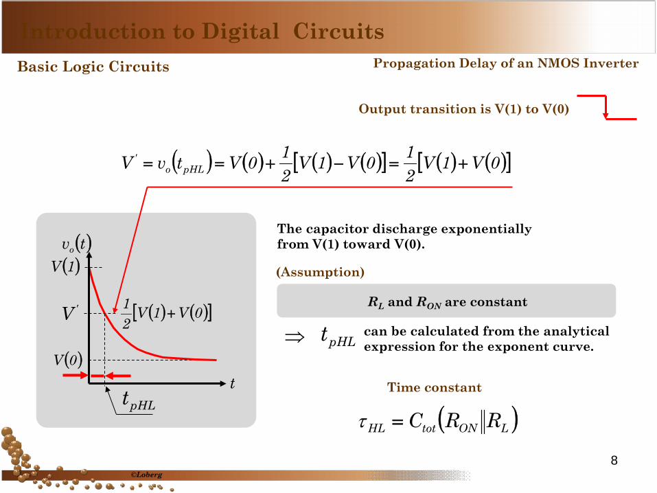
( ) ( ) ( ) ( )[ ] ( ) ( )[ ]0V1V210V1V
210VtvV pHLo
' +=−+==
( )0V
( )1V
( ) ( )[ ]0V1V21
+
( )tvo
tpHLt
'V
Output transition is V(1) to V(0)
Time constant
( )LONtotHL RRC=τ
The capacitor discharge exponentially from V(1) toward V(0).
RL and RON are constant
can be calculated from the analytical expression for the exponent curve. pHLt⇒
(Assumption)
©Loberg
Introduction to Digital Circuits Basic Logic Circuits Propagation Delay of an NMOS Inverter
8
Output transition is V(0) to V(1)
totC must be charged toward V(1) .
( ) ( )1VVtv DDo ==∞=
©Loberg
Introduction to Digital Circuits Basic Logic Circuits Propagation Delay of an NMOS Inverter
Input transition is V(1) to V(0)
( )0V
( )1V( )tvo
tpLHt
switch is open
( ) ( )[ ]0V1V21
+
( ) ( )0VRR
RV0tvONL
ONDDo =
+==
9
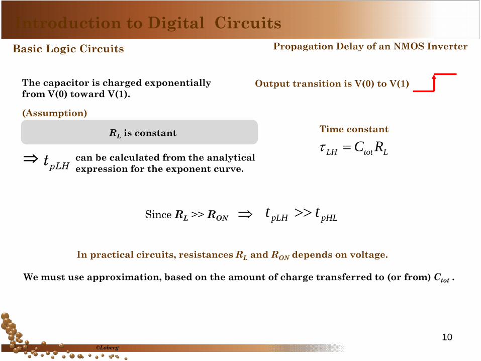
The capacitor is charged exponentially from V(0) toward V(1).
RL is constant
can be calculated from the analytical expression for the exponent curve. pLHt⇒
(Assumption)
Since RL >> RON ⇒ pHLpLH tt >>
In practical circuits, resistances RL and RON depends on voltage.
We must use approximation, based on the amount of charge transferred to (or from) Ctot .
Output transition is V(0) to V(1)
Time constant
LtotLH RC=τ
©Loberg
Introduction to Digital Circuits Basic Logic Circuits Propagation Delay of an NMOS Inverter
10
totC
Li
DDV+
LR
ONR
DiCi
Driver
Load
ovControlled switch
Input
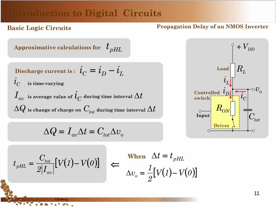
Discharge current is : LDC iii −=is time-varying Ci
avI is average value of during time interval Ci t∆Q∆ is change of charge on totC during time interval t∆
ototav vCtIQ ∆∆∆ ==
pHLtt =∆
( ) ( )[ ]0V1V21vo −=∆
When ⇐( ) ( )[ ]0V1V
I2Ct
av
totpHL −=
Approximative calculations for pHLt
©Loberg
Introduction to Digital Circuits Basic Logic Circuits Propagation Delay of an NMOS Inverter
11
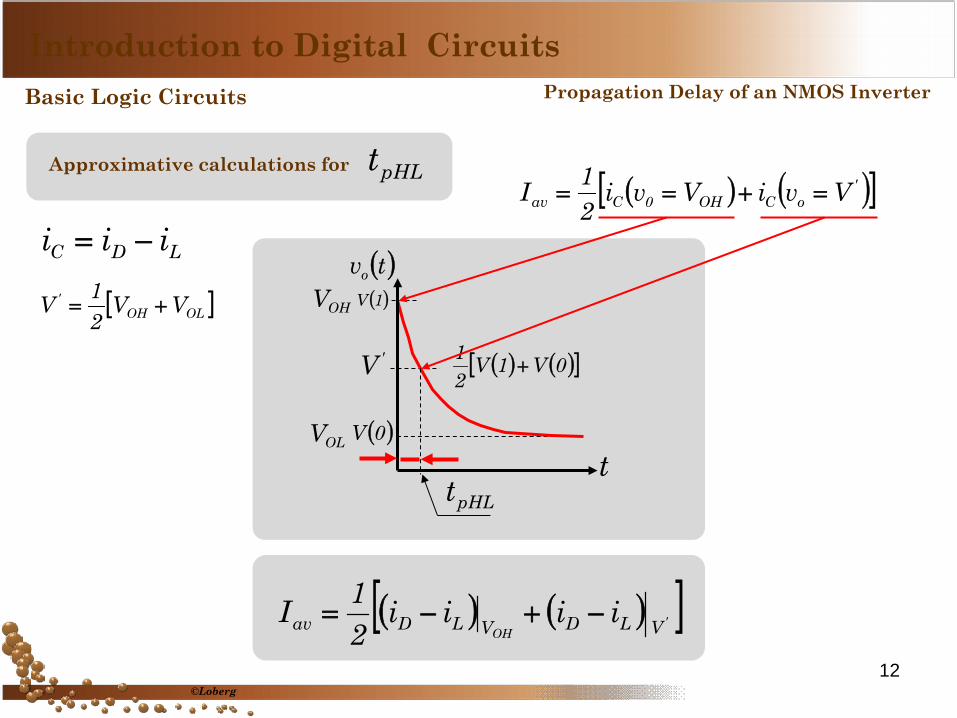
LDC iii −=
[ ]OLOH' VV
21V +=
( ) ( )[ ]'OH VLDVLDav iiii
21I −+−=
( ) ( )[ ]'oCOH0Cav VviVvi
21I =+==
( )0V
( )1V
( ) ( )[ ]0V1V21
+
( )tvo
tpHLt
'V
OHV
OLV
©Loberg
Introduction to Digital Circuits Basic Logic Circuits Propagation Delay of an NMOS Inverter
Approximative calculations for pHLt
12
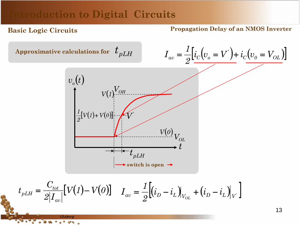
( ) ( )[ ]'OL VLDVLDav iiii
21I −+−=( ) ( )[ ]0V1V
I2Ct
av
totpLH −=
©Loberg
Introduction to Digital Circuits Basic Logic Circuits Propagation Delay of an NMOS Inverter
Approximative calculations for pLHt ( ) ( )[ ]OL0C'
oCav VviVvi21I =+==
( )0V
( )1V
( )tvo
tpLHt
switch is open
OLV
OHV
'V( ) ( )[ ]0V1V21
+
13
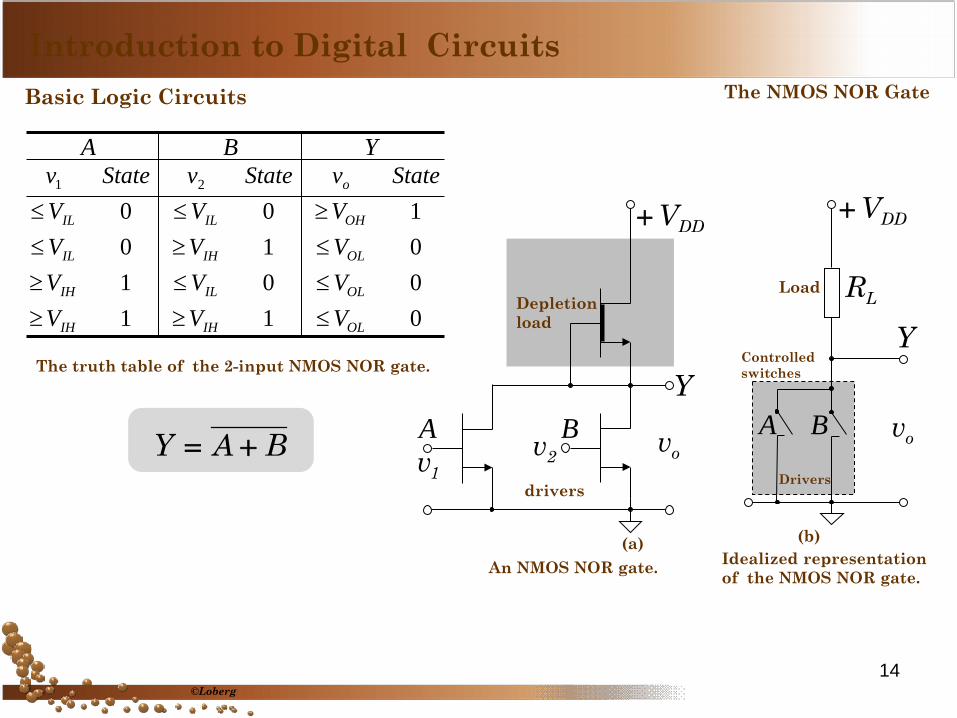
The NMOS NOR Gate
(a)
ov2v
DDV+
Depletion load
drivers 1v
YA B
An NMOS NOR gate.
DDV+
LRY
Drivers
Load
ov
Controlled switches
A B
(b) Idealized representation of the NMOS NOR gate.
011001010100
21
OLIHIH
OLILIH
OLIHIL
OHILIL
o
VVVVVVVVVVVV
StatevStatevStatev
≤≥≥≤≤≥≤≥≤≥≤≤
A B Y
The truth table of the 2-input NMOS NOR gate.
BAY +=
©Loberg
Introduction to Digital Circuits Basic Logic Circuits
14
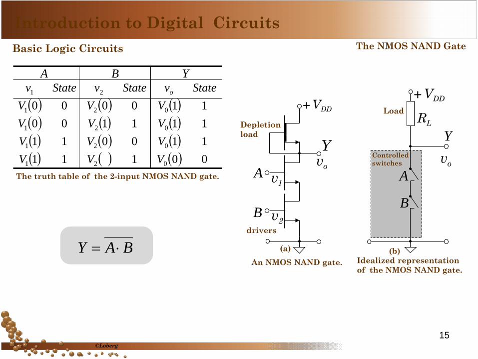
(a)
ov
2vdrivers
DDV+Depletion load
Y
1vA
B
An NMOS NAND gate.
DDV+
LRY
Load
ovControlled switches
A
B
(b) Idealized representation of the NMOS NAND gate.
( ) ( ) ( )( ) ( ) ( )( ) ( ) ( )( ) ( ) ( ) 00111
110011111100110000
021
021
021
021
21
VVVVVVVVVVVV
StatevStatevStatev o
A B Y
The truth table of the 2-input NMOS NAND gate.
BAY ⋅=
©Loberg
Introduction to Digital Circuits Basic Logic Circuits The NMOS NAND Gate
15
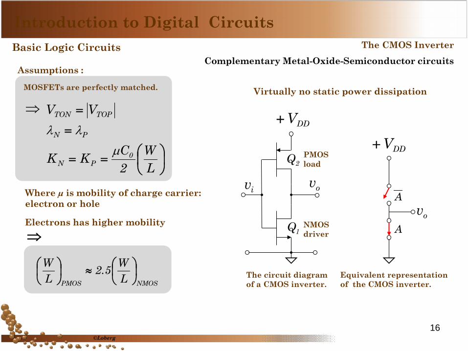
The CMOS Inverter
ov
DDV+
A
A
Equivalent representation of the CMOS inverter.
DDV+
PMOS load
NMOS driver
2Q
1Q
oviv
The circuit diagram of a CMOS inverter.
Complementary Metal-Oxide-Semiconductor circuits
Virtually no static power dissipation
Assumptions :
MOSFETs are perfectly matched.
⇒
==
=
=
LW
2CKK
VV
0PN
PN
TOPTON
µλλ
Where µ is mobility of charge carrier: electron or hole
Electrons has higher mobility ⇒
NMOSPMOS LW5.2
LW
≈
©Loberg
Introduction to Digital Circuits Basic Logic Circuits
16
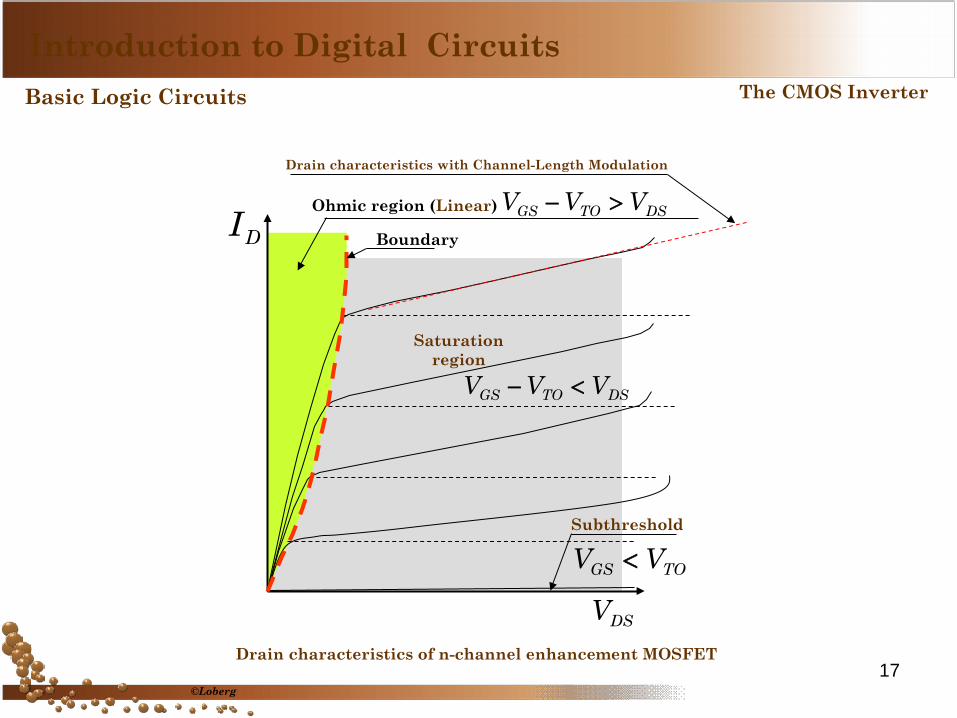
Drain characteristics with Channel-Length Modulation
Drain characteristics of n-channel enhancement MOSFET
Ohmic region (Linear) DSTOGS VVV >−
DSV
Saturation region
DI
Subthreshold
Boundary
TOGS VV <
DSTOGS VVV <−
©Loberg
Introduction to Digital Circuits Basic Logic Circuits The CMOS Inverter
17
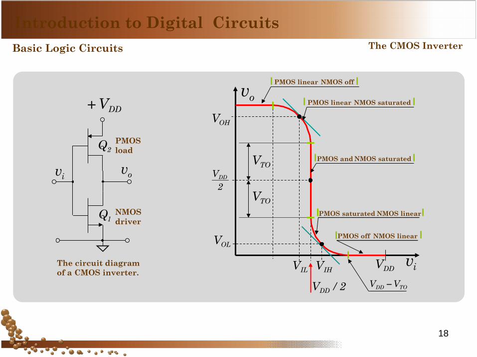
Introduction to Digital Circuits The CMOS Inverter Basic Logic Circuits
DDV iv
ov PMOS linear NMOS off
PMOS linear NMOS saturated
PMOS and NMOS saturated
PMOS saturated NMOS linear
PMOS off NMOS linear
IHVILV
OHV
OLV
2VDD
2/VDD
TOV
TOV
TODD VV −
DDV+
PMOS load
NMOS driver
2Q
1Q
oviv
The circuit diagram of a CMOS inverter.
18
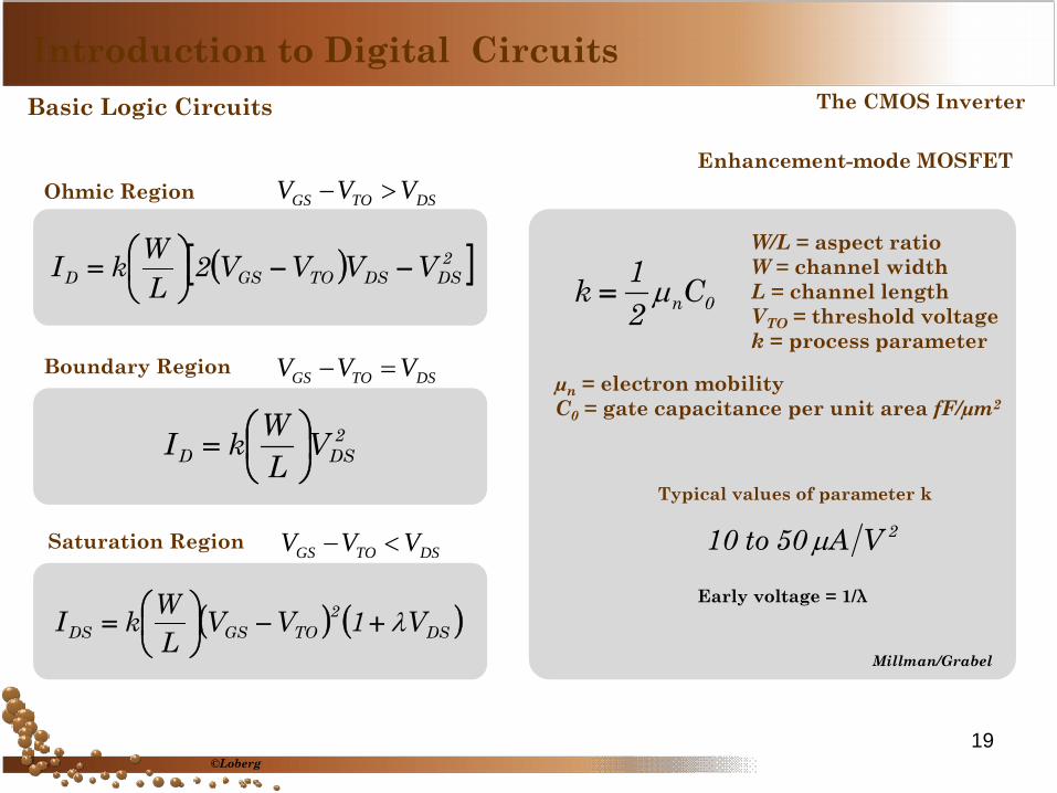
Ohmic Region
( )[ ]2DSDSTOGSD VVVV2
LWkI −−
=
DSTOGS VVV >−
Boundary Region
2DSD V
LWkI
=
DSTOGS VVV =−
( ) ( )DS2
TOGSDS V1VVLWkI λ+−
=
Saturation Region DSTOGS VVV <−
W/L = aspect ratio W = channel width L = channel length VTO = threshold voltage k = process parameter
Typical values of parameter k
2VA50to10 µ
0nC21k µ=
µn = electron mobility C0 = gate capacitance per unit area fF/µm2
Early voltage = 1/λ
Enhancement-mode MOSFET
©Loberg
Introduction to Digital Circuits Basic Logic Circuits The CMOS Inverter
Millman/Grabel
19
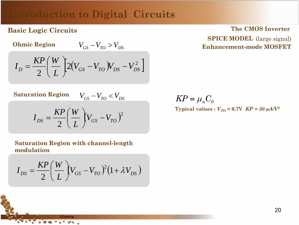
Ohmic Region
( )[ ]222 DSDSTOGSD VVVV
LWKPI −−
=
DSTOGS VVV >−SPICE MODEL
( )22 TOGSDS VV
LWKPI −
=
Saturation Region DSTOGS VVV <−
( ) ( )DSTOGSDS VVVL
WKPI λ+−
= 1
22
Saturation Region with channel-length modulation
Typical values : VTO = 0.7V KP = 30 µA/V2 0nCKP µ=
(large signal) Enhancement-mode MOSFET
©Loberg
Introduction to Digital Circuits Basic Logic Circuits The CMOS Inverter
20
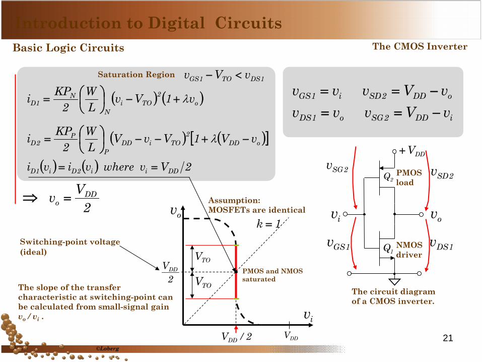
iDD2SGo1DS
oDD2SDi1GS
vVvvvvVvvv
−==
−==
DDV+
PMOS load
NMOS driver
2Q
1Q
oviv
The circuit diagram of a CMOS inverter.
1GSv
2SGv2SDv
1DSv
( ) ( )o2
TOiN
N1D v1Vv
LW
2KPi λ+−
=
Saturation Region 1DSTO1GS vVv <−
( ) ( )[ ]oDD2
TOiDDP
P2D vV1VvV
LW
2KPi −+−−
= λ
⇒
( ) ( ) 2Vvwherevivi DDii2Di1D ==
2Vv DD
o =
Switching-point voltage (ideal)
The slope of the transfer characteristic at switching-point can be calculated from small-signal gain vo / vi .
ov
DDV
iv
PMOS and NMOS saturated 2
VDD
2/VDD
TOV
TOV
1k =
Assumption: MOSFETs are identical
©Loberg
Introduction to Digital Circuits Basic Logic Circuits The CMOS Inverter
21
1S2S
1G2G
iVoV+
- +
+
+
- -
- 2gsV 1gsV
2gs2m Vg 1gs1m Vg
1dr 2dr
oI
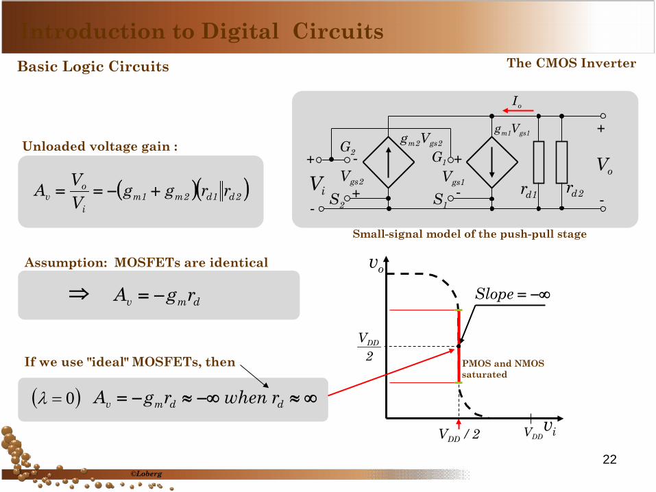
Small-signal model of the push-pull stage
( )( )2d1d2m1mi
ov rrgg
VVA +−==
Assumption: MOSFETs are identical
⇒ dmv rgA −=
Unloaded voltage gain :
If we use "ideal" MOSFETs, then
∞≈−∞≈−= ddmv rwhenrgA( )0=λ
ov
DDV iv
PMOS and NMOS saturated
2/VDD
−∞=Slope
2VDD
©Loberg
Introduction to Digital Circuits Basic Logic Circuits The CMOS Inverter
22
ov
DDViv
2VDD
2/VDD
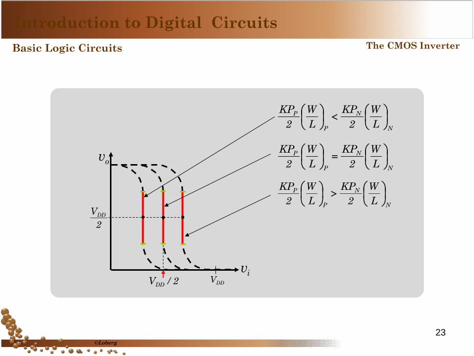
N
N
P
P
LW
2KP
LW
2KP
<
N
N
P
P
LW
2KP
LW
2KP
=
N
N
P
P
LW
2KP
LW
2KP
>
©Loberg
Introduction to Digital Circuits Basic Logic Circuits The CMOS Inverter
23
Power Dissipation of CMOS Logic
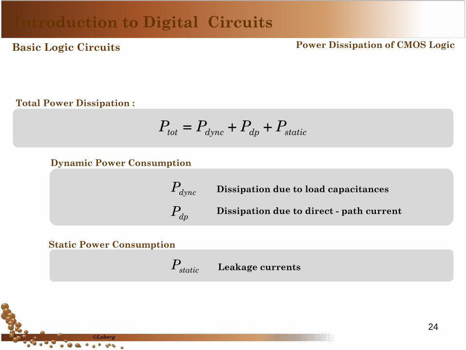
staticdpdynctot PPPP ++=
Dynamic Power Consumption
Total Power Dissipation :
Static Power Consumption
dyncP
dpPDissipation due to load capacitances
Dissipation due to direct - path current
Leakage currents staticP
©Loberg
Introduction to Digital Circuits Basic Logic Circuits
24
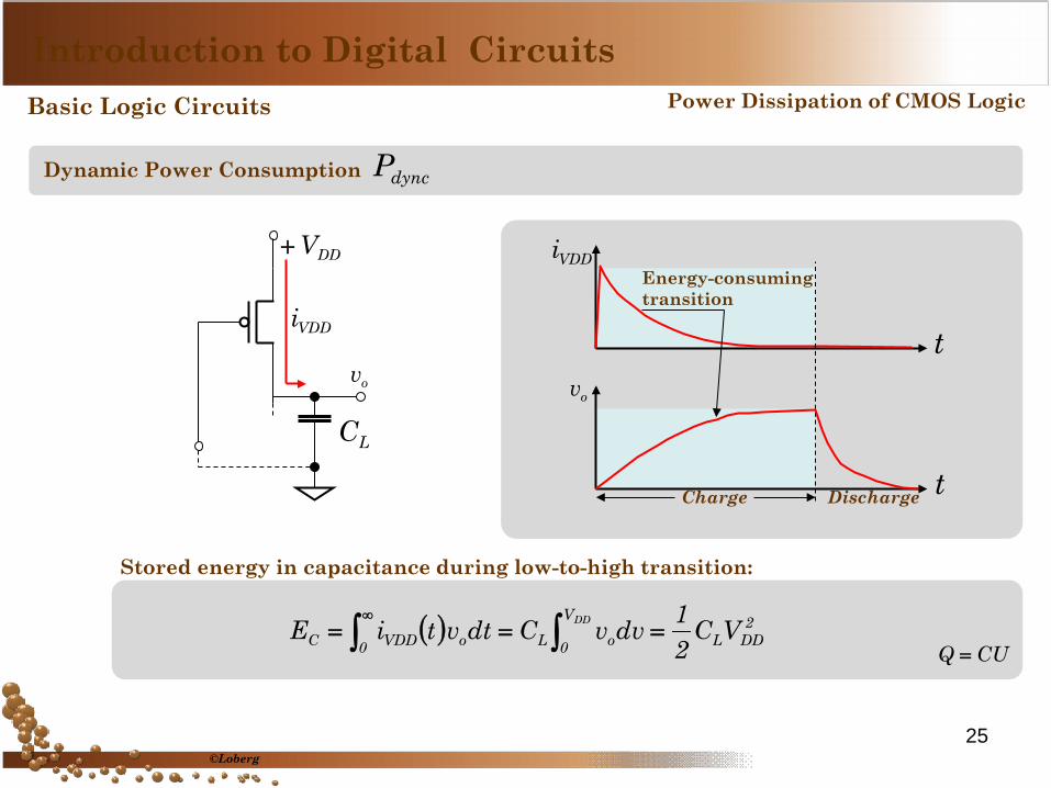
( ) 2DDL
V
0 oLo0 VDDC VC21dvvCdtvtiE DD
=== ∫∫∞
DDV+
VDDi
ov
LC
Dynamic Power Consumption dyncP
Stored energy in capacitance during low-to-high transition:
CUQ =
VDDi
ov
Charge Discharge
Energy-consuming transition
t
t
©Loberg
Introduction to Digital Circuits Basic Logic Circuits Power Dissipation of CMOS Logic
25
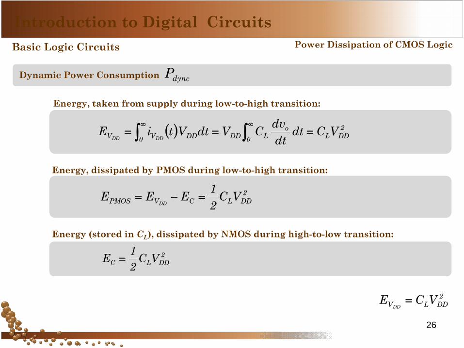
Introduction to Digital Circuits Basic Logic Circuits Power Dissipation of CMOS Logic
Dynamic Power Consumption dyncP
( ) 2DDL0
oLDDDD0 VV VCdt
dtdvCVdtVtiE
DDDD=== ∫∫
∞∞
Energy, taken from supply during low-to-high transition:
2DDLC VC
21E =
2DDLV VCE
DD=
2DDLCVPMOS VC
21EEE
DD=−=
Energy, dissipated by PMOS during low-to-high transition:
Energy (stored in CL), dissipated by NMOS during high-to-low transition:
26
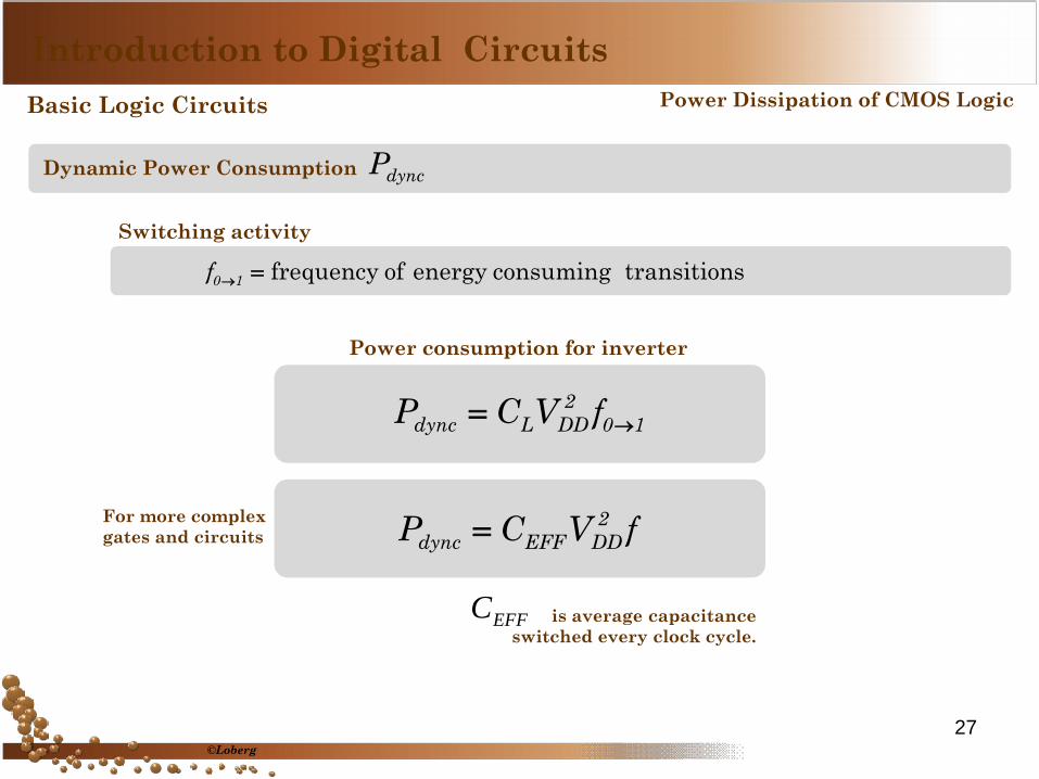
102
DDLdync fVCP →=
Power consumption for inverter
fVCP 2DDEFFdync =
is average capacitance switched every clock cycle.
EFFC
For more complex gates and circuits
stransitionconsumingenergyoffrequency=→10fSwitching activity
©Loberg
Introduction to Digital Circuits Basic Logic Circuits Power Dissipation of CMOS Logic
Dynamic Power Consumption dyncP
27
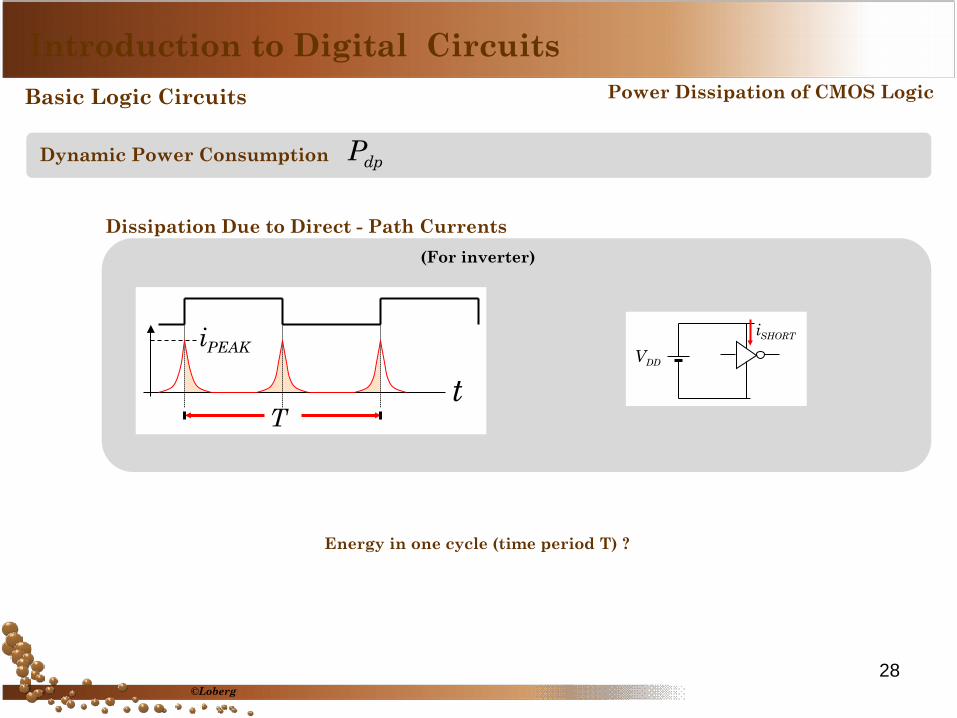
Dissipation Due to Direct - Path Currents (For inverter)
SHORTi
DDV
T
PEAKi
t
Energy in one cycle (time period T) ?
©Loberg
Introduction to Digital Circuits Basic Logic Circuits Power Dissipation of CMOS Logic
Dynamic Power Consumption dpP
28
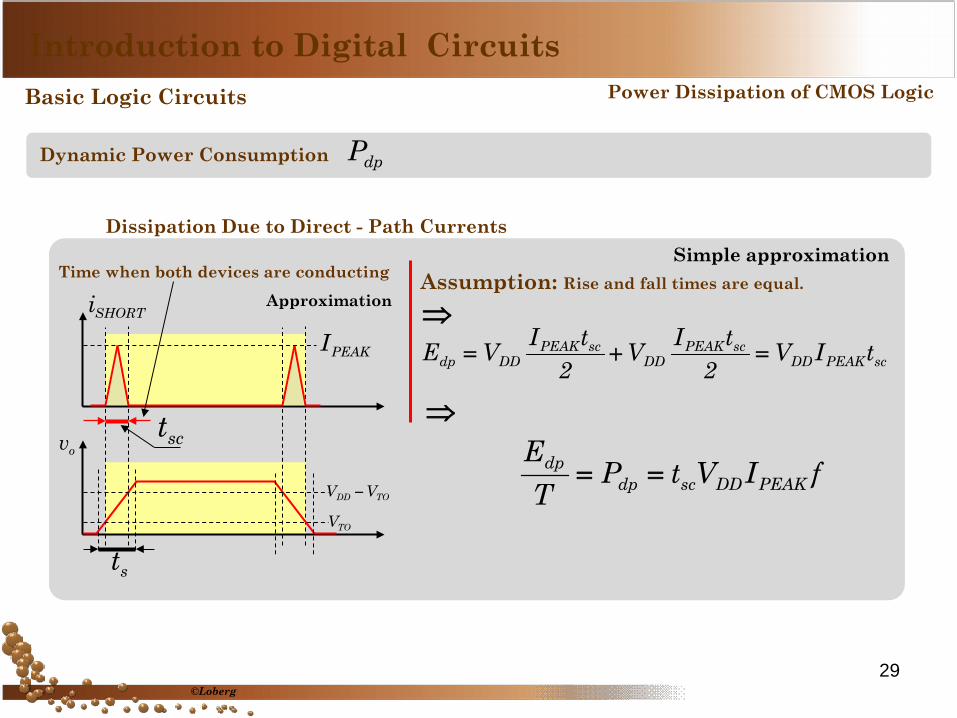
fIVtPT
EPEAKDDscdp
dp ==
Simple approximation
scPEAKDDscPEAK
DDscPEAK
DDdp tIV2
tIV2
tIVE =+=
Assumption: Rise and fall times are equal.
⇒SHORTi
ov
PEAKI
TOVTODD VV −
st
sct
Time when both devices are conducting Approximation
⇒
©Loberg
Introduction to Digital Circuits Basic Logic Circuits Power Dissipation of CMOS Logic
Dissipation Due to Direct - Path Currents
Dynamic Power Consumption dpP
29
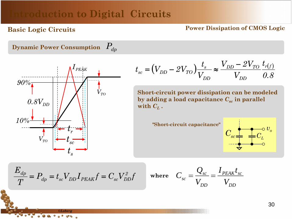
DD
scPEAK
DD
scsc V
tIVQC ==where
( ) ( )
8.0t
VV2V
VtV2Vt fr
DD
TODD
DD
sTODDsc
−≈−=
"Short-circuit capacitance"
Short-circuit power dissipation can be modeled by adding a load capacitance Csc in parallel with CL .
ovscC
LC
fVCfIVtPT
E 2DDscPEAKDDscdp
dp ===
©Loberg
Introduction to Digital Circuits Basic Logic Circuits Power Dissipation of CMOS Logic
Dynamic Power Consumption dpP
30
%10
%90
rt
st
DDV8.0
sct
PEAKI
TOV
TOV
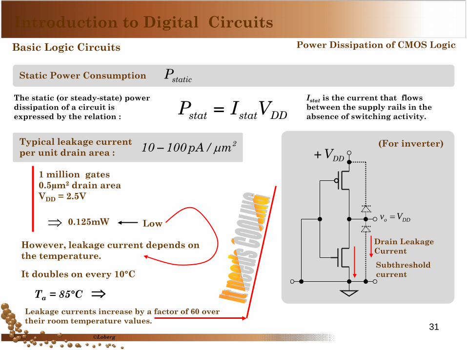
Static Power Consumption staticP
The static (or steady-state) power dissipation of a circuit is expressed by the relation : DDstatstat VIP =
DDV+
DDo Vv =
Subthreshold current
Drain Leakage Current
Typical leakage current per unit drain area :
2m/pA10010 µ−
1 million gates 0.5µm2 drain area VDD = 2.5V
⇒ 0.125mW
However, leakage current depends on the temperature.
It doubles on every 10°C
Ta = 85°C Leakage currents increase by a factor of 60 over their room temperature values.
⇒
Istat is the current that flows between the supply rails in the absence of switching activity.
(For inverter)
Low
©Loberg
Introduction to Digital Circuits Basic Logic Circuits Power Dissipation of CMOS Logic
Static Power Consumption staticP
31
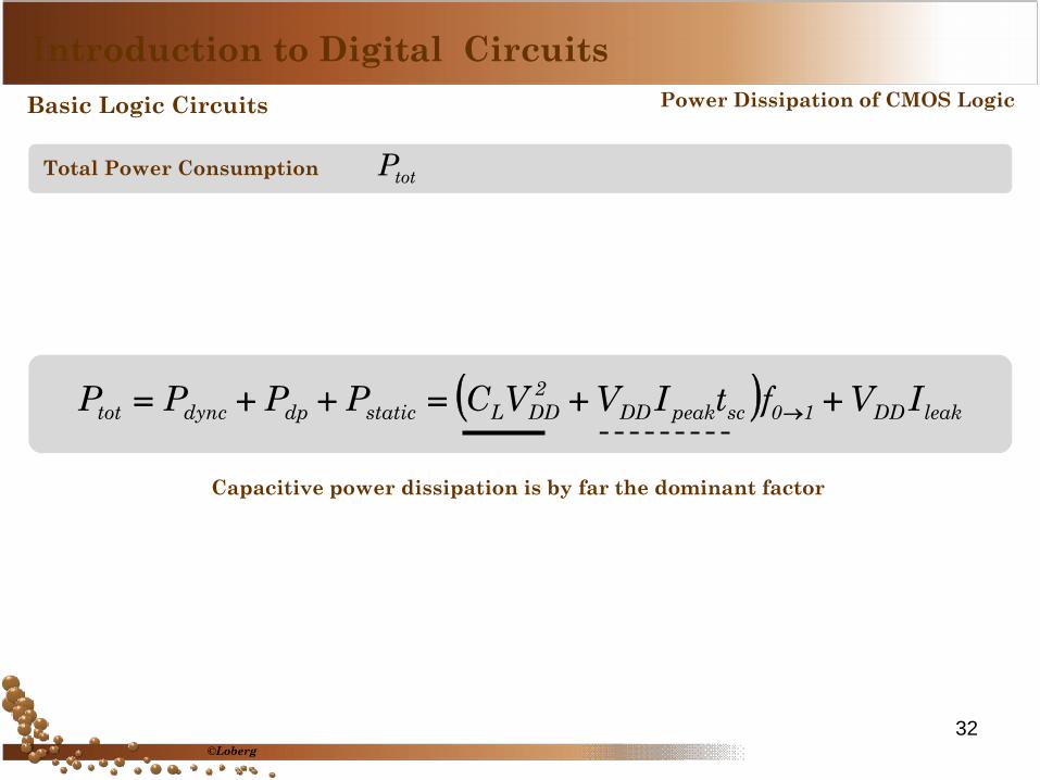
Capacitive power dissipation is by far the dominant factor
( ) leakDD10scpeakDD2
DDLstaticdpdynctot IVftIVVCPPPP ++=++= →
©Loberg
Introduction to Digital Circuits Basic Logic Circuits Power Dissipation of CMOS Logic
Total Power Consumption totP
32

33
The End