1 Revision 1.0, 2015-10-03
About this document
Scope and purpose
This application note describes Infineon’s Antenna Switch Module BGSF1717MN26 as main antenna switch
module for multi-mode GSM/EDGE, WCDMA or LTE Applications and Carrier Aggregation applications.
1. This application notes gives an overview about main purpose of this
SP7T Low Band + SP7T High Band Antenna Switch Module.
2. Multi-mode GSM/EDGE, WCDMA or LTE Applications and Carrier Aggregation are the primary
application of this document. 3. The Printed Circuit Board (PCB) design as well as antenna matching network proposed in this note
provides a customer oriented approach where a single ASM enables multi-mode GSM/EDGE, WCDMA or LTE and Carrier Aggregation applications
4. Key performance parameters include higher Isolation between input channels (~32dB), integrated
SAW Filter for LB and HB GSM Tx inputs, very low IL of the TX channels (0.5dB), integration of SP7T LB and SP7T HB in one module and an integrated MIPI RFFE Interface.
Ante n na S wi t ch Mo d ule : BG S F1 717 M N2 6
Ante n na S wi t ch Mo d ule wi th i n tegra ted
MI PI RFFE Int er fa ce, 2 G SM TX Ports for
mult i -m od e GS M/ ED GE, W CD M A or L TE
Appl i cat io ns a nd Car r ier A g gre gat io n
Solut i ons
Application Note AN384

Antenna Switch Module with integrated MIPI RFFE Interface
Table of Content
Application Note AN384 2 Revision 1.0, 2015-10-03
Table of Content
About this document ................................................................................................................... 1
1 Introduction of BGSF1717MN26 .................................................................................... 5
1.1 Main Features ...................................................................................................................................... 5 1.2 Functional Diagram ............................................................................................................................. 6 1.3 Pin Configuration ................................................................................................................................ 7
1.4 Pin Description .................................................................................................................................... 7
2 Application ................................................................................................................. 9
3 Application Circuit of BGSF1717MN26 ......................................................................... 10
3.1 Application Board ............................................................................................................................. 10 3.2 Deembedding .................................................................................................................................... 11 3.2.1 Deembedding concept with a “prepared” SMA connector and a “Half-Thru” boardPort
Extension ..................................................................................................................................... 11
3.2.2 Deembedding control process ................................................................................................... 12
4 Small Signal Characteristics of BGSF1717MN26 ............................................................ 13
4.1 Small Signal Parameters LB switch .................................................................................................. 13
4.1.1 Insertion Loss from LB Antenna to the respective RF TRX Port ................................................ 13 4.1.2 Insertion Loss TX LB port ............................................................................................................ 14
4.1.3 Insertion Loss high linearity ultra low IL TRx10 port ................................................................. 14 4.1.4 Return Loss from LB Antenna to the respective RF Port ........................................................... 15
4.1.5 Return Loss of LB TRX RF ports to LB Antenna .......................................................................... 16
4.1.6 Return Loss TX LB RF port ........................................................................................................... 16
4.1.7 Antenna to port and Port to Port Isolation LB path .................................................................. 18 4.2.6 Antenna to port and Port to Port Isolation HB path .................................................................. 25
5 Non-Linear performance of BGSF1717MN26 ................................................................. 28 5.1 Intermodulation ................................................................................................................................ 28
5.1.1 Intermodulation Measurement Setup ......................................................................................... 29
5.1.2 Intermodulation Measurement conditions for Band I ............................................................... 30
5.1.3 Intermodulation Measurement Results for Band I .................................................................... 30 5.1.4 Intermodulation Measurement conditions for Band V .............................................................. 31 5.1.5 Intermodulation Measurement Results for Band V ................................................................... 31
5.2 Harmonic Distortion ........................................................................................................................... 32
5.2.1 Harmonic Generation Measurement conditions ......................................................................... 32
5.2.2 Harmonic Generation Measurement Results of Low Band inputs .............................................. 33 5.2.3 Harmonic Generation Measurement Results of High Band inputs ............................................. 35
6 Switching time.......................................................................................................... 36
7 Appendix: Switch Controller Unit ................................................................................ 37
7.1 Operating Guide ................................................................................................................................. 37
7.2 Display Settings of the Controller Unit .............................................................................................. 38
8 Authors .................................................................................................................... 39
Revision History ......................................................................................................................... 40
Antenna Switch Module with integrated MIPI RFFE Interface
List of Figures and Tables
Application Note AN384 3 Revision 1.0, 2015-10-03
List of Figures
Figure 1 BGSF1717MN26 in TSNP-26-3 ............................................................................................................. 5
Figure 2 BGSF1717MN26 Functional Diagram ................................................................................................. 6 Figure 3 BGSF1717MN26 Pin Configuration .................................................................................................... 7 Figure 4 BGSF1717MN26 in mobile phone cellular frontend (typical discrete LTE-A feature set) ................. 9
Figure 5 Layout of the application board ....................................................................................................... 10
Figure 6 PCB Layer stack-up ........................................................................................................................... 10 Figure 7 “Half-Thru” deembedding board ..................................................................................................... 12 Figure 8 “Full-Thru” deembedding board ...................................................................................................... 12 Figure 9 Application circuit BGSF1717MN26 .................................................................................................. 13
Figure 10 Forward transmission from LB Antenna to TX LB port .................................................................... 13 Figure 11 Forward transmission from LB Antenna to TX LB port .................................................................... 14 Figure 12 Forward transmission from LB Antenna to TRX10 port ................................................................... 15
Figure 13 Return Loss from LB Antenna to the respective TRX LB RF port ..................................................... 15
Figure 14 Return Loss of LB TRX RF ports to LB Antenna ................................................................................ 16 Figure 15 Return Loss port TX LB RF port ......................................................................................................... 17 Figure 16 Return Loss of high linearity ultra low IL TRX10 RF port ................................................................. 17
Figure 17 Worst case Antenna to Port Isolation Low Band part ...................................................................... 20
Figure 18 Worst case Port to Port Isolation Low Band part1 ........................................................................... 20
Figure 19 Forward transmission from HB Antenna to the respective TRX HB RF port ................................... 21 Figure 20 Forward transmission from HB Antenna to the respective TX HB RF port ..................................... 22
Figure 21 Return Loss from HB Antenna to the respective TRX HB RF port .................................................... 23 Figure 22 Return Loss from HB TRX RF ports to HB Antenna .......................................................................... 24
Figure 23 Return Loss of HB TX RF port ............................................................................................................ 24 Figure 24 Worst case Antenna to Port Isolation High Band part ..................................................................... 27
Figure 25 Worst case Port to Port Isolation High Band part1 ........................................................................... 27 Figure 26 Block diagram of RF Switch intermodulation .................................................................................. 29
Figure 27 Intermodulation Measurement Test Setup ...................................................................................... 29
Figure 28 Intermodulation measurement results for Band I ........................................................................... 30 Figure 29 Intermodulation measurement results for Band V .......................................................................... 31 Figure 30 Harmonic Generation Measurement setup ...................................................................................... 32 Figure 31 Measurements of Harmonic power over Carrier power of Low-Band inputs to LB Antenna ......... 33
Figure 32 Harmonic power measurements of high linear LB input TRX10 over the Band 17 carrier ............. 34
Figure 33 Measurements of Harmonic power over Carrier power of High-Band inputs to HB Antenna ....... 35 Figure 34 Switching time measurements of the TX_LB input to the LB Antenna ........................................... 36 Figure 35 Switch Controller Unit Board ............................................................................................................ 37
Antenna Switch Module with integrated MIPI RFFE Interface
List of Figures and Tables
Application Note AN384 4 Revision 1.0, 2015-10-03
List of Tables Table 1 Pin Description (top view) ................................................................................................................... 7
Table 2 Insertion Loss from LB Antenna to TX LB port ................................................................................. 13 Table 3 Insertion loss from LB Antenna to TX LB port .................................................................................. 14 Table 4 Insertion loss from LB Antenna to TRx10 port ................................................................................. 14
Table 5 Return loss from LB Antenna to the respective TRX LB RF port ...................................................... 15 Table 6 Return loss from respective TRX LB RF port to LB Antenna ............................................................ 16
Table 7 Return loss from TR LB RF port ......................................................................................................... 16 Table 8 Return loss from TRX10 RF port ........................................................................................................ 17
Table 9 Worst case Antenna to Port Isolation High Band part ..................................................................... 18
Table 10 Worst case Port to Port Isolation Low Band part ............................................................................. 19
Table 11 Insertion Loss from HB Antenna to the respective TRX HB RF port ................................................ 21 Table 12 Insertion Loss from HB Antenna to the respective TX HB RF .......................................................... 22 Table 13 Return Loss from HB Antenna to the respective TRX HB RF port ................................................... 23 Table 14 Return Loss from HB TRX RF ports to HB Antenna .......................................................................... 23
Table 15 Return Loss of HB TX RF port ............................................................................................................ 24
Table 16 Worst case Antenna to Port Isolation High Band part ..................................................................... 25
Table 17 Worst case Port to Port Isolation High Band part ............................................................................ 26 Table 18 Test conditions and specifications of IMD measurements .............................................................. 30 Table 19 Typical and maximal value of intermodulation products in dBm for Band I ................................. 30
Table 20 Test conditions and specifications of IMD measurements .............................................................. 31 Table 21 Typical and maximal value of intermodulation products in dBm for Band V................................ 31
Table 22 Harmonic Generation measurement Conditions ............................................................................ 32
Table 23 Switching time values ....................................................................................................................... 36
Table 24 Seeting Display of Active RF Path, Power UP, Power Down and Isolation State ............................ 38

Antenna Switch Module with integrated MIPI RFFE Interface
Introduction of BGSF1717MN26
Application Note AN384 5 Revision 1.0, 2015-10-03
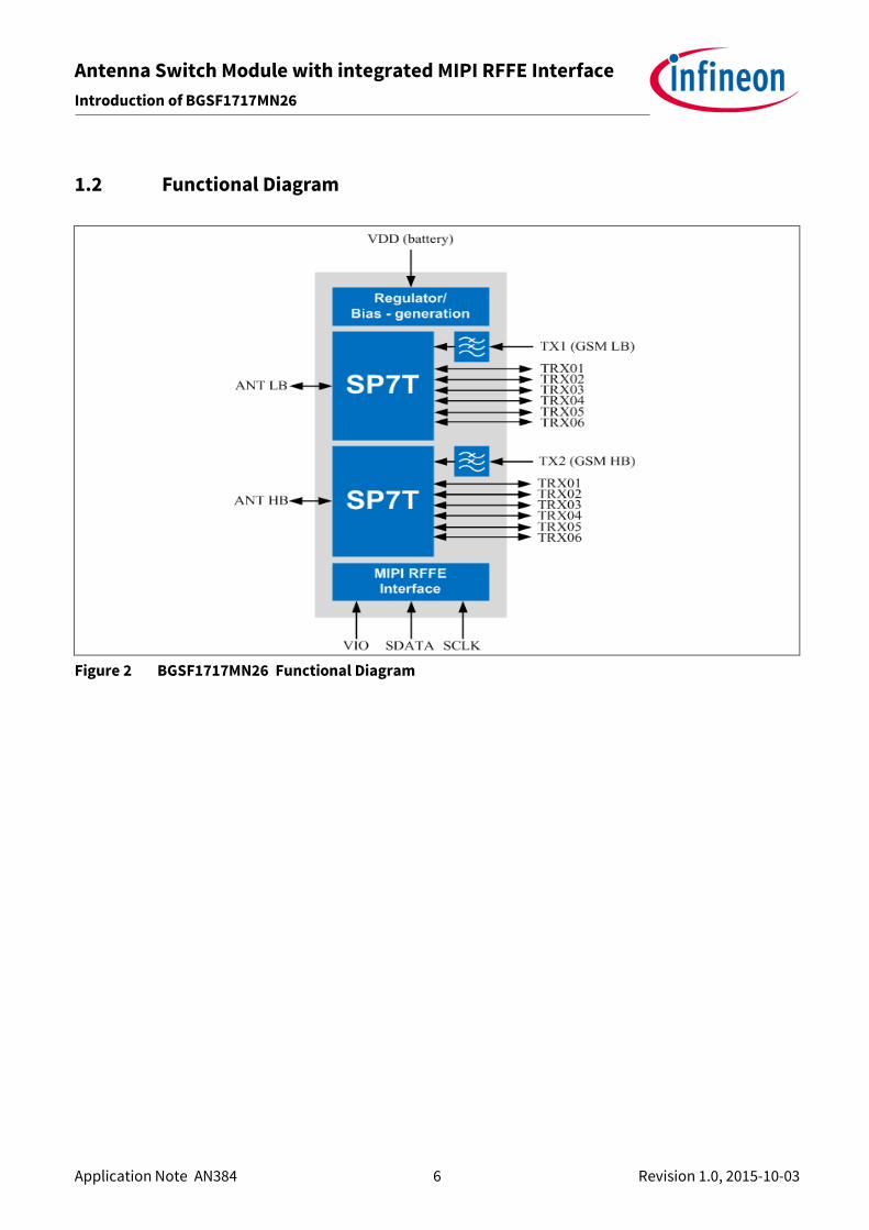
1 Introduction of BGSF1717MN26
For RF Front-End solutions that integrate new features such as downlink inter-band carrier aggregation to increase Downlink data rates, Antenna Switch Modules (ASMs) are facing new challenges. Two RF signals
being transmitted in different frequency bands have to be routed from two different antennas – one dedicated for low frequency band and one for high frequency band - to the RF Transceiver at the same time.
For this kind of application, the new switch which combines two SP7T ICs and the MIPI control interface, the so-called DP14T, have been introduced to the market.
The BGSF1717MN26 is a double Pole Fourteen Throw (DP14T / SP7T+SP7T) ASM optimized for wireless applications up to 2.7 GHz. It is a perfect solution for multi-mode handsets based on quad-band GSM,
WCDMA, LTE and ideal for carrier aggregation solutions. TRX10 is designed to achieve ultra-high linearity. The ASM configuration is shown in the Figure 2.
The module comes in a miniature TSNP package shown in the Figure 1 and comprises of two high power SP7T switches with integrated MIPI RFFE interface and harmonic filters for GSM high and low band
transmitter signal paths. The on-chip MIPI RFFE interface supports both 1.2 V and 1.8 V supply voltages. No external DC blocking capacitors are required in typical applications as long as no DC is applied to any RF
port. The pin assignment can be found in the Figure 3.
1.1 Main Features
• Suitable for multi-mode GSM / EDGE / C2K /
WCDMA / LTE applications and carrier
aggregation
Operating from 0.1 to 2.7 GHz coverage
• Ultra-low insertion loss and harmonics
generation
• Integrated GSM transmit filters
• 12 interchangeable, high-linearity WCDMA TRX ports
• Port TRX10 designed for ultra-high linearity
• 2 high-linearity GSM TX paths
• High port-to-port isolation
• Integrated MIPI RFFE interface
• No decoupling DC capacitors required, if no DC applied on RF lines
• Small form factor: 3.2 mm x 2.8 mm x 0.73 mm
Figure 1 BGSF1717MN26 package in TSNP-26-3
Antenna Switch Module with integrated MIPI RFFE Interface
Introduction of BGSF1717MN26
Application Note AN384 6 Revision 1.0, 2015-10-03
1.2 Functional Diagram
Figure 2 BGSF1717MN26 Functional Diagram

Antenna Switch Module with integrated MIPI RFFE Interface
Introduction of BGSF1717MN26
Application Note AN384 7 Revision 1.0, 2015-10-03
1.3 Pin Configuration
Figure 3 BGSF1717MN26 Pin Configuration
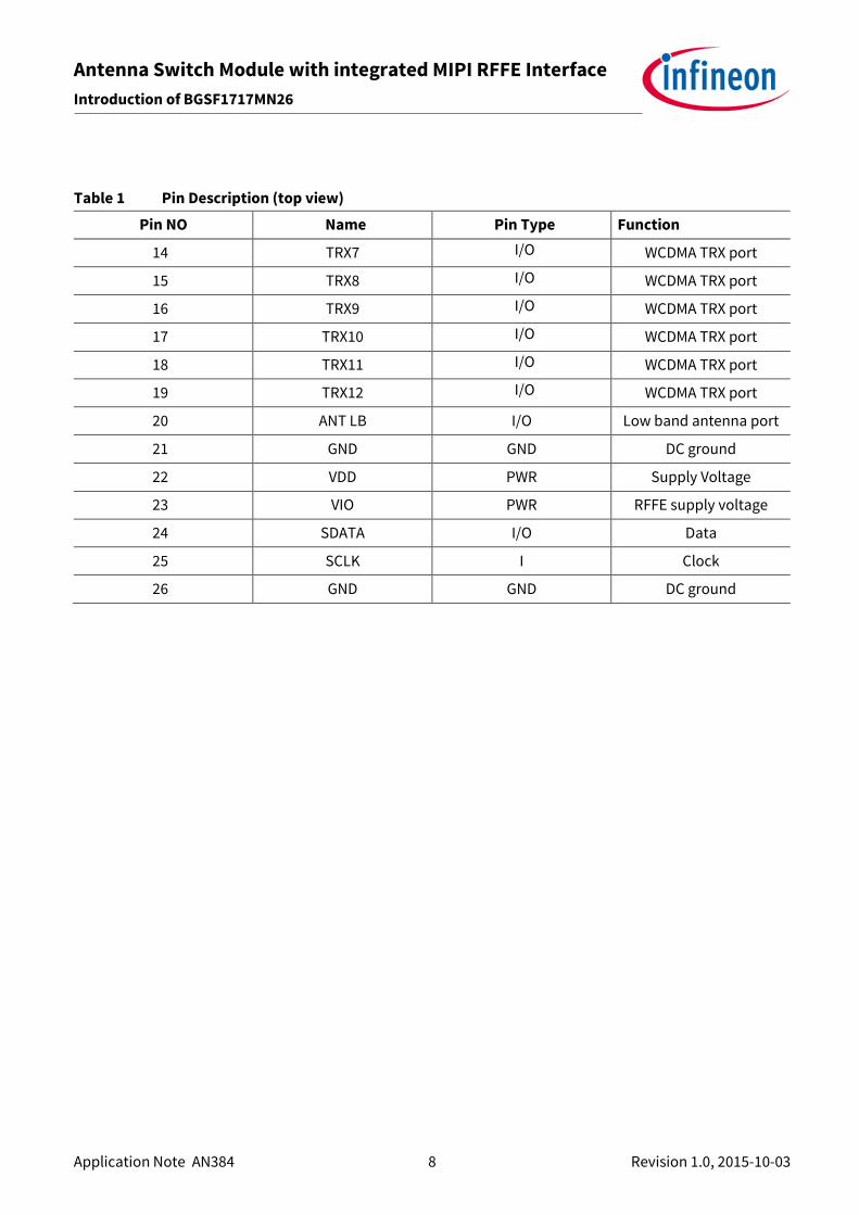
1.4 Pin Description
Table 1 Pin Description (top view)
Pin NO Name Pin Type Function
0 GND GND Ground, die pad
1 GND GND DC ground
2 ANT HB I/O High band antenna port
3 TRX6 I/O WCDMA TRX port
4 TRX5 I/O WCDMA TRX port
5 TRX4 I/O WCDMA TRX port
6 TRX3 I/O WCDMA TRX port
7 TRX2 I/O WCDMA TRX port
8 TRX1 I/O WCDMA TRX port
9 GND GND RF ground
10 TXHB I GSM HB port
11 GND GND RF ground
12 TXLB I GSM LB port
13 GND GND RF ground
14 813 12 11 10 9
21 122 23 24 25 26
15
16
17
18
19
20
7
6
5
4
3
2
2.8 x 3.2 x 0.73 mm
GND pad
GND TXLB GND TXHB GND
VDD VIO SDATA SCLK GND
TRX7
TRX8
TRX9
TRX10
TRX11
TRX12
ANT LB ANT HB
TRX6
TRX5
TRX4
TRX3
TRX2
GND
TRX1
GND
Antenna Switch Module with integrated MIPI RFFE Interface
Introduction of BGSF1717MN26
Application Note AN384 8 Revision 1.0, 2015-10-03
Table 1 Pin Description (top view)
Pin NO Name Pin Type Function
14 TRX7 I/O WCDMA TRX port
15 TRX8 I/O WCDMA TRX port
16 TRX9 I/O WCDMA TRX port
17 TRX10 I/O WCDMA TRX port
18 TRX11 I/O WCDMA TRX port
19 TRX12 I/O WCDMA TRX port
20 ANT LB I/O Low band antenna port
21 GND GND DC ground
22 VDD PWR Supply Voltage
23 VIO PWR RFFE supply voltage
24 SDATA I/O Data
25 SCLK I Clock
26 GND GND DC ground

Antenna Switch Module with integrated MIPI RFFE Interface
Application
Application Note AN384 9 Revision 1.0, 2015-10-03
2 Application
A typical application of BGSF1717MN26 ASM in a mobile phone is shown in the Figure 4. At the main
antenna path of the RF Front-End the BGSF1717MN26 switches signals from the high band and low band
antenna to the different transceiver IC input and outputs. For the diversity path different Infineon RF
switches can be used e.g. BGS16MN14, BGS18MN14. Infineon offers also besides ASMs, general purpose RF
Switches and a broad portfolio of Low Noise Amplifiers and Antenna Tuner Devices. All of Infineon Products
concerning mobile phone applications can be found in our newest Application Guide for RF & Protection
Devices/ Mobile Communication.
Figure 4 BGSF1717MN26 in mobile phone cellular frontend (typical discrete LTE-A feature set)
ASMPowered by
Tranceiver 1 Transciever 2
Tx/Rx SPDT
Tx/Rx DPDT
LTE LNA LTE
LNA
GNSS
LNA Diversity Switches
(SPxT)
Antenna Switch Module
BGSF1717MN26
Antenna Aperture Switches (SPxT)
Tx/Rx SPDT
HB LB
Antenna Switch Module with integrated MIPI RFFE Interface Application Circuit of BGSF1717MN26
Application Note AN384 10 Revision 1.0, 2015-10-03
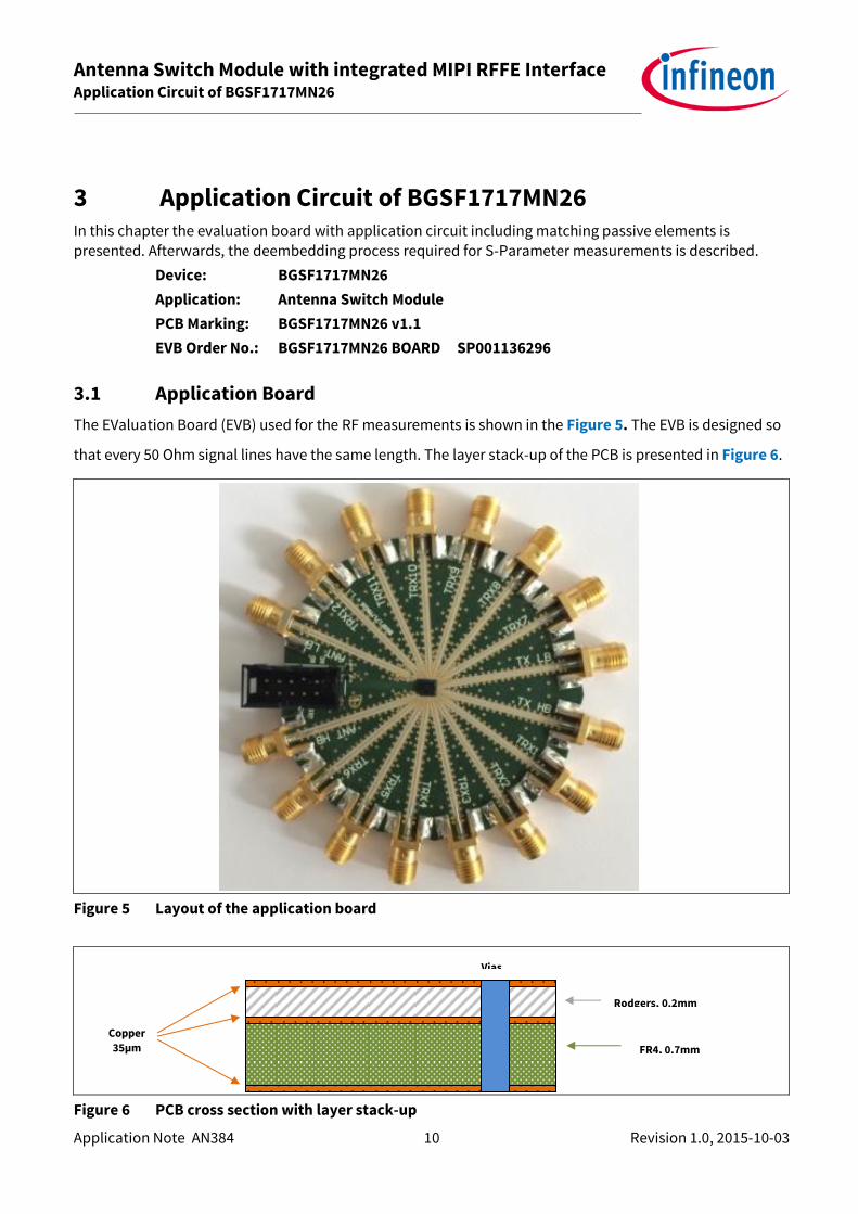
3 Application Circuit of BGSF1717MN26 In this chapter the evaluation board with application circuit including matching passive elements is presented. Afterwards, the deembedding process required for S-Parameter measurements is described.
Device: BGSF1717MN26
Application: Antenna Switch Module
PCB Marking: BGSF1717MN26 v1.1
EVB Order No.: BGSF1717MN26 BOARD SP001136296
3.1 Application Board
The EValuation Board (EVB) used for the RF measurements is shown in the Figure 5. The EVB is designed so
that every 50 Ohm signal lines have the same length. The layer stack-up of the PCB is presented in Figure 6.
Figure 5 Layout of the application board
Figure 6 PCB cross section with layer stack-up
Copper
35µm
Rodgers, 0.2mm
FR4, 0.7mm
Vias

Antenna Switch Module with integrated MIPI RFFE Interface Application Circuit of BGSF1717MN26
Application Note AN384 11 Revision 1.0, 2015-10-03
3.2 Deembedding
The device (BGSF1717MN26) is deembedded from influence of the application circuit and coaxial
connectors by at first measuring a coaxial connector and a “half-board” micro strip line and then by loading
this data in the fixture simulator of the network analyzer. In the Figure 7 this deembedding concept is given.
The deembedding of this RF device is performed in several steps explained in the next subchapters.
Figure 7 Deembedding concept with a “prepared” SMA connector and a “Half-Thru” board
3.2.1 Port Extension
In order to shift the reference plane of the network analyzer to the PCB signal line connect a SMA connector
with a cut pin of the inner conductor to one port of the Vector Network Analyzer (VNA) and measure port
extensions at this port.
Figure 8 shows such a “prepared” SMA connector with an outer pin cut with a wire cutter.
Outer
conductor
pin is cut
Antenna Switch Module with integrated MIPI RFFE Interface Application Circuit of BGSF1717MN26
Application Note AN384 12 Revision 1.0, 2015-10-03
Figure 8 SMA connector with cut inner pin
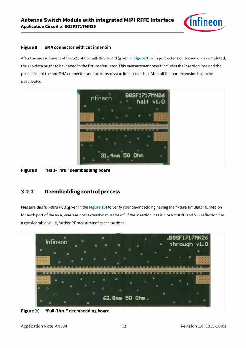
After the measurement of the S21 of the half-thru board (given in Figure 9) with port extension turned on is completed,
the s2p-data ought to be loaded in the fixture simulator. This measurement result includes the insertion loss and the
phase shift of the one SMA connector and the transmission line to the chip. After all the port extension has to be
deactivated.
Figure 9 “Half-Thru” deembedding board
3.2.2 Deembedding control process
Measure this full-thru PCB (given in the Figure 10) to verify your deembedding having the fixture simulator turned on
for each port of the VNA, whereas port extension must be off. If the insertion loss is close to 0 dB and S11 reflection has
a considerable value, further RF measurements can be done.
Figure 10 “Full-Thru” deembedding board

Antenna Switch Module with integrated MIPI RFFE Interface Small Signal Characteristics of BGSF1717MN26
Application Note AN384 13 Revision 1.0, 2015-10-03
4 Small Signal Characteristics of BGSF1717MN26
The S-Parameters are measured at 25 °C with a VNA in an application circuit shown in Figure 11.
68 nH 1.5 pF
2.7 pF
2.4 nH
Low Band
AntennaHigh Band
Antenna
5.1 nH
Figure 11 Application circuit BGSF1717MN26
4.1 Small Signal Parameters LB switch
4.1.1 Insertion Loss from LB Antenna to the respective RF TRX Port
Table 2 Insertion Loss from LB Antenna to TX LB port
Frequency (MHz)
704 716 740 751 824 881 915 942
TRx7 -0.76 -0.76 -0.74 -0.74 -0.75 -0.75 -0.75 -0.76
TRx8 -0.74 -0.74 -0.72 -0.73 -0.73 -0.74 -0.74 -0.74
TRx9 -0.72 -0.71 -0.69 -0.7 -0.7 -0.71 -0.71 -0.71
TRx11 -0.67 -0.66 -0.64 -0.65 -0.66 -0.66 -0.66 -0.66 TRx12 -0.65 -0.65 -0.63 -0.64 -0.64 -0.64 -0.64 -0.64
Figure 12 Forward transmission from LB Antenna to TX LB port
0.0003 2 4 6 8 10
Frequency (GHz)
Insertion Loss TRx LB paths
-50
-40
-30
-20
-10
0
2.1 GHz-28.21 dB
0.6 GHz-0.6967 dB
0.96 GHz-0.6515 dB
TR7
TRx8
TRx9
TRx11
TRx12
Unused ports are
terminated with 50Ω

Antenna Switch Module with integrated MIPI RFFE Interface Small Signal Characteristics of BGSF1717MN26
Application Note AN384 14 Revision 1.0, 2015-10-03
4.1.2 Insertion Loss TX LB port
Table 3 Insertion loss from LB Antenna to TX LB port
Frequency (MHz)
704 716 740 751 824 881 915 942
TR LB -1.37 -1.39 -1.42 -1.45 -1.51 -1.52 -1.51 -1.51
Figure 13 Forward transmission from LB Antenna to TX LB port
4.1.3 Insertion Loss high linearity ultra-low IL TRx10 port
Table 4 Insertion loss from LB Antenna to TRx10 port
Frequency (MHz)
704 716 740 751 824 881 915 942
TR LB -0.56 -0.56 -0.54 -0.55 -0.55 -0.56 -0.55 -0.56
0.0003 2 4 6 8 10
Frequency (GHz)
Insertion Loss Tx LB
-60
-50
-40
-30
-20
-10
0
Insert
ion L
oss (
dB
)
2.17 GHz-40.76 dB
1.71 GHz-41 dB
0.915 GHz-1.51 dB
0.824 GHz-1.508 dB
Antenna Switch Module with integrated MIPI RFFE Interface Small Signal Characteristics of BGSF1717MN26
Application Note AN384 15 Revision 1.0, 2015-10-03
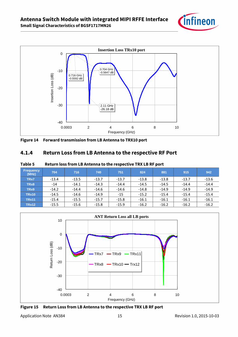
Figure 14 Forward transmission from LB Antenna to TRX10 port
4.1.4 Return Loss from LB Antenna to the respective RF Port
Table 5 Return loss from LB Antenna to the respective TRX LB RF port
Frequency (MHz)
704 716 740 751 824 881 915 942
TRx7 -13.4 -13.5 -13.7 -13.7 -13.8 -13.8 -13.7 -13.6
TRx8 -14 -14.1 -14.3 -14.4 -14.5 -14.5 -14.4 -14.4
TRx9 -14.2 -14.4 -14.6 -14.6 -14.8 -14.9 -14.9 -14.9
TRx10 -14.5 -14.6 -14.9 -15 -15.2 -15.4 -15.4 -15.4
TRx11 -15.4 -15.5 -15.7 -15.8 -16.1 -16.1 -16.1 -16.1
TRx12 -15.5 -15.6 -15.8 -15.9 -16.2 -16.2 -16.2 -16.2
Figure 15 Return Loss from LB Antenna to the respective TRX LB RF port
0.0003 2 4 6 8 10
Frequency (GHz)
ANT Return Loss all LB ports
-40
-30
-20
-10
0
10
Re
turn
Lo
ss (
dB
)
TRx7
TRx8
TRx9
TRx10
TRx11
Trx12
0.0003 2 4 6 8 10
Frequency (GHz)
Insertion Loss TRx10 port
-40
-30
-20
-10
0In
sert
ion L
oss (
dB
)
2.11 GHz-26.18 dB
0.704 GHz-0.5647 dB
0.716 GHz-0.5592 dB
Antenna Switch Module with integrated MIPI RFFE Interface Small Signal Characteristics of BGSF1717MN26
Application Note AN384 16 Revision 1.0, 2015-10-03
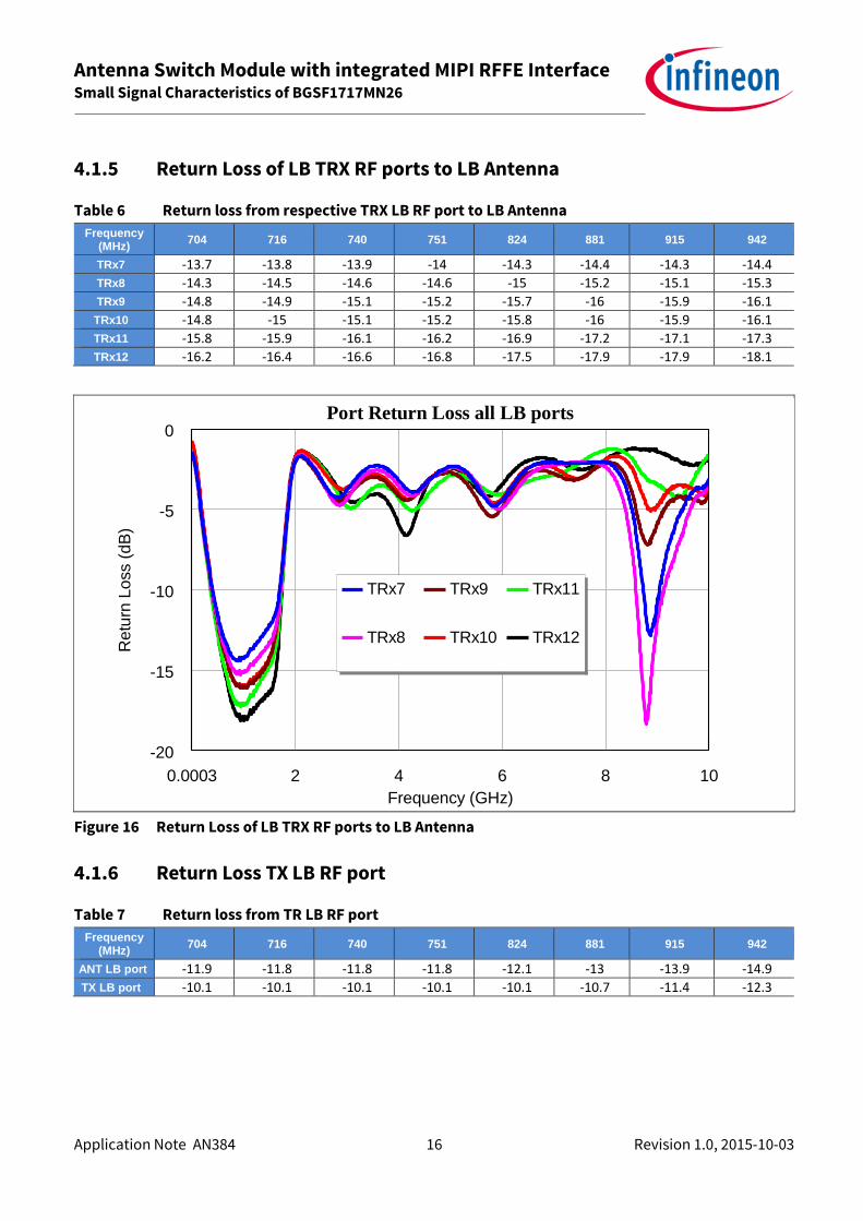
4.1.5 Return Loss of LB TRX RF ports to LB Antenna
Table 6 Return loss from respective TRX LB RF port to LB Antenna
Frequency (MHz)
704 716 740 751 824 881 915 942
TRx7 -13.7 -13.8 -13.9 -14 -14.3 -14.4 -14.3 -14.4
TRx8 -14.3 -14.5 -14.6 -14.6 -15 -15.2 -15.1 -15.3
TRx9 -14.8 -14.9 -15.1 -15.2 -15.7 -16 -15.9 -16.1
TRx10 -14.8 -15 -15.1 -15.2 -15.8 -16 -15.9 -16.1
TRx11 -15.8 -15.9 -16.1 -16.2 -16.9 -17.2 -17.1 -17.3
TRx12 -16.2 -16.4 -16.6 -16.8 -17.5 -17.9 -17.9 -18.1
Figure 16 Return Loss of LB TRX RF ports to LB Antenna
4.1.6 Return Loss TX LB RF port
Table 7 Return loss from TR LB RF port
Frequency (MHz)
704 716 740 751 824 881 915 942
ANT LB port -11.9 -11.8 -11.8 -11.8 -12.1 -13 -13.9 -14.9
TX LB port -10.1 -10.1 -10.1 -10.1 -10.1 -10.7 -11.4 -12.3
0.0003 2 4 6 8 10
Frequency (GHz)
Port Return Loss all LB ports
-20
-15
-10
-5
0
Retu
rn L
oss (
dB
)
TRx7
TRx8
TRx9
TRx10
TRx11
TRx12

Antenna Switch Module with integrated MIPI RFFE Interface Small Signal Characteristics of BGSF1717MN26
Application Note AN384 17 Revision 1.0, 2015-10-03
Figure 17 Return Loss port TX LB RF port
Table 8 Return loss from TRX10 RF port
Frequency (MHz)
704 716 740 751 824 881 915 942
ANT LB port -14.5 -14.6 -14.9 -15 -15.2 -15.4 -15.4 -15.4
TRX10 port -14.8 -15 -15.1 -15.2 -15.8 -16 -15.9 -16.1
Figure 18 Return Loss of high linearity ultra-low IL TRX10 RF port
0.0003 2 4 6 8 10
Frequency (GHz)
Return Loss TX LB
-40
-30
-20
-10
0
10
Re
turn
Lo
ss (
dB
)
0.89027 GHz-10.7 dB
0.942 GHz-12.26 dB
Antenna LB
TX LB
0.0003 2 4 6 8 10
Frequency (GHz)
Return Loss TRX10
-20
-15
-10
-5
0
5
Re
turn
Loss (
dB
)
Antenna LB
TRX10

Antenna Switch Module with integrated MIPI RFFE Interface Small Signal Characteristics of BGSF1717MN26
Application Note AN384 18 Revision 1.0, 2015-10-03
4.1.7 Antenna to port and Port to Port Isolation LB path
Apply to the Table 9 and Table 10 on the next page.
1 Worst case isolation: Isolation between neighbor port of the active port, any other port have better (higher) Isolation
Table 9 Worst case Antenna to Port Isolation High Band part1
Frequency
(GHz)
TX HB active TRX1 active TRX2 active TRX3 active TRX4 active TRX5 active TRX6 active
ANTHB
TRX1
ANTHB
TX LB
ANTHB
TRX2
ANTHB
TX HB
ANTHB
TRX3
ANTHB
TRX1
ANTHB
TRX4
ANTHB
TRX2
ANTHB
TRX5
ANTHB
TRX3
ANTHB
TRX6
ANTHB
TRX4
ANTHB
ANT LB
ANTHB
TRX5
0.704 -39.5 -39.7 -47.2 -34.2 -37.3 -35.5 -34.1 -35 -33.4 -38.3 -42.7 -43.2 -39.3 -37
0.716 -39.3 -39.6 -46.9 -33.9 -37.1 -35.4 -34 -34.8 -33.3 -38.4 -42.3 -42.9 -39.1 -36.8
0.74 -38.9 -39.8 -47 -33.8 -36.6 -35.2 -33.8 -34.6 -33 -38 -42.3 -42.6 -39 -36.5
0.751 -38.6 -39.6 -46.4 -33.7 -36.7 -35.1 -33.7 -34.4 -32.9 -37.9 -42 -42.1 -38.7 -36.2
0.824 -37.4 -39.3 -45.2 -32.9 -35.9 -34.3 -32.9 -33.8 -32.3 -37.1 -41.3 -40.5 -37.9 -35.3
0.881 -36.3 -39.4 -44.1 -32.5 -35.2 -33.9 -32.5 -33.4 -31.8 -36.6 -40.5 -39.2 -37.3 -34.5
0.915 -35.8 -39.9 -43.6 -32.2 -35.1 -33.5 -32.2 -33.1 -31.5 -36.3 -40.2 -38.6 -36.9 -34.1
0.942 -35.4 -40.2 -43.5 -31.9 -34.8 -33.2 -32 -32.8 -31.3 -36 -39.8 -38.2 -36.8 -33.8
1.71 -45.4 -30.2 -45 -29.9 -33.1 -30.6 -29.5 -30 -28.6 -32.4 -35.7 -29.8 -32.7 -29.1
1.842 -46.5 -32.7 -48 -31.3 -34.3 -32 -31 -31.5 -30.2 -34 -37.1 -30.9 -34.3 -31.1
1.96 -50 -36.8 -53.3 -36.5 -39.6 -37.3 -36.3 -36.8 -35.3 -39.3 -42.9 -36.7 -40 -37.5
1.97 -50.2 -37.2 -54.5 -37.3 -40.2 -38 -37 -37.5 -36 -39.9 -43.8 -37.4 -40.5 -38.4
2.017 -52.8 -40.4 -60.7 -41.8 -44.9 -42.2 -41.4 -41.8 -40.5 -44.2 -48.9 -42.4 -45.4 -42.9
2.14 -54.6 -41.1 -61.9 -46.5 -48.6 -47 -46.2 -47.1 -45.3 -48.9 -51.4 -44.1 -49.7 -48.2
2.17 -49.8 -36 -63.9 -43.7 -46 -44.1 -43.1 -43.2 -41.9 -45.8 -49.1 -41.5 -46.6 -45.6
2.35 -34.7 -19.9 -53.2 -35.1 -37.6 -36 -34.6 -35.1 -33.7 -37.5 -42.2 -34.5 -39.2 -38.8
2.593 -40.9 -24.8 -49.3 -30.7 -32.9 -31.3 -29.9 -30.5 -29.3 -33.1 -38 -30.1 -34.5 -36.3
2.69 -42.4 -26 -47.9 -29.5 -31.5 -29.9 -28.7 -29.2 -28.1 -31.6 -36.5 -28.9 -33.1 -35.6
3.5 -56.4 -28.9 -44.2 -26.2 -27.6 -26.2 -25.2 -25.5 -24.9 -27 -29.7 -22.9 -25.6 -30.4

Antenna Switch Module with integrated MIPI RFFE Interface Small Signal Characteristics of BGSF1717MN26
Application Note AN384 19 Revision 1.0, 2015-10-03
Table 10 Worst case Port to Port Isolation Low Band part1
Frequency
(GHz)
TX LB active TRX7 active TRX8 active TRX9 active TRX10 active TRX11 active TRX12 active
ANTLB
TX HB
ANTLB
TRX7
ANTLB
TX LB
ANTLB
TRX8
ANTLB
TRX7
ANTLB
TRX9
ANTLB
TRX8
ANTLB
TRX10
ANTLB
TRX9
ANTLB
TRX11
ANTLB
TRX10
ANTLB
TRX12
ANTLB
TRX11
ANTLB
ANTHB
0.704 -39.6 -39.8 -40.9 -32.3 -34.9 -33.5 -32.1 -30.5 -31.4 -35.8 -35.2 -39.7 -36.2 -37.8
0.716 -39.6 -39.9 -41.1 -32.2 -34.7 -33.3 -31.9 -30.4 -31.3 -35.7 -35 -39.8 -36.2 -37.6
0.74 -39 -39.8 -40.5 -31.9 -34.4 -33 -31.7 -30.1 -31 -35.3 -34.8 -39.2 -35.9 -37.3
0.751 -39 -39.9 -40.5 -31.7 -34.4 -32.9 -31.7 -30 -30.9 -35.3 -34.7 -39.1 -35.8 -37.1
0.824 -37.8 -39.7 -40.4 -31.1 -33.7 -32.1 -30.9 -29.3 -30.2 -34.6 -33.9 -38 -34.9 -36.2
0.881 -36.7 -39.8 -40.7 -30.5 -33.1 -31.6 -30.3 -28.7 -29.6 -33.9 -33.4 -37.2 -34.2 -35.6
0.915 -36 -39.6 -40.8 -30.2 -32.7 -31.3 -30 -28.4 -29.3 -33.6 -33.1 -36.7 -33.9 -35.3
0.942 -35.6 -39.5 -41.2 -30.1 -32.6 -31.1 -29.8 -28.2 -29.1 -33.4 -32.8 -36.2 -33.7 -34.9
1.71 -35 -37.8 -46.1 -28 -28.8 -27.4 -27.3 -24.9 -26.7 -29.7 -28 -27.2 -29.5 -26.8
1.842 -35.2 -37.7 -48.1 -25.3 -26.3 -24.7 -24.9 -22.9 -24.5 -26.8 -25.8 -23.7 -26.6 -24.7
1.96 -35.2 -37.4 -43.4 -21.9 -23.5 -21.8 -21.6 -20.2 -21 -23.9 -23.9 -21.9 -24 -24.6
1.97 -35 -37.3 -43.5 -21.7 -23.4 -21.6 -21.4 -20.1 -20.8 -23.7 -23.9 -21.9 -23.9 -24.7
2.017 -35.2 -37.3 -42.2 -21 -22.8 -20.9 -20.5 -19.3 -19.9 -23.1 -23.5 -21.8 -23.4 -25.1
2.14 -35.1 -36.2 -40.3 -19.8 -22 -20 -19.3 -18.2 -18.4 -22.1 -23.1 -21.9 -22.6 -26.8
2.17 -35.4 -35.8 -40.2 -19.7 -21.9 -19.9 -19.1 -18 -18.2 -22 -23.1 -22 -22.5 -27.3
2.35 -34.3 -35.9 -39.2 -19 -21.5 -19.4 -18.2 -17.1 -17.3 -21.4 -22.7 -22.4 -21.9 -29.7
2.593 -33.2 -39.2 -38.8 -18.5 -21.6 -19.2 -17.6 -16.5 -16.5 -21 -22.4 -22.9 -21.1 -32.5
2.69 -32.8 -38.2 -38.9 -18.7 -21.9 -19.3 -17.7 -16.6 -16.5 -21 -22.3 -23.4 -20.8 -33.9
3.5 -30.9 -38.5 -45.8 -26.4 -25.5 -25.7 -25.8 -22.2 -24.6 -27.2 -24.9 -22.5 -26.3 -30.8
1 Worst case isolation: Isolation between neighbor port of the active port, any other port have better (higher) Isolation

Antenna Switch Module with integrated MIPI RFFE Interface Small Signal Characteristics of BGSF1717MN26
Application Note AN384 20 Revision 1.0, 2015-10-03
Figure 19 Worst case Antenna to Port Isolation Low Band part1
Figure 20 Worst case Port to Port Isolation Low Band part1
1 Worst case isolation: Isolation between neighbor port of the active port, any other port have better (higher) Isolation
0.0003 2 4 6 8 10
Frequency (GHz)
Isolation LB paths to LB paths
-100
-80
-60
-40
-20
0
Isola
tion
(dB
)
TXHB to TXLBLB active
TRx7 to TXLBLB active
TXLB to TRx7TRx7 active
TRx8 to TRx7TRX7 active
TRx7 to TRx8TRx8 active
TRX9 to TRx8TRX8 active
TRx8 to TRx9TRx9 active
TRx10 to TRx9TRx9 active
TRx9 to TRx10TRx10 active
TRx9 to TRx10TRx10 active
TRx10 to TRx11TRx11 active
TRx12 to TRx11TRx11 active
TRx11 to TRx12TRx12 active
ANTHB to TRx12TRx12 active
0.0003 2 4 6 8 10
Frequency (GHz)
Isolation ANT to LB paths
-100
-80
-60
-40
-20
0
Isola
tion (
dB
)
TXHB to ANTLBLB active
TRx7 to ANTLBLB active
TXLB to ANT LBTRx7 active
TRx8 to ANTLBTRX7 active
TRx7 to ANTLBTRx8 active
TRX9 to ANTLBTRX8 active
TRx8 to ANTLBTRx9 active
TRx10 to ANTLBTRx9 active
TRx9 to ANT LBTRx10 active
TRx9 to ANTLBTRx10 active
TRx10 to ANTLBTRx11 active
TRx12 to ANTLBTRx11 active
TRx11 to ANTLBTRx12 active
ANTHB to ANTLBTRx12 active

Antenna Switch Module with integrated MIPI RFFE Interface Small Signal Characteristics of BGSF1717MN26
Application Note AN384 21 Revision 1.0, 2015-10-03
4.2 Small Signal Parameters HB switch
4.2.1 Insertion Loss from HB Antenna to the respective TRX HB RF Port
Table 11 Insertion Loss from HB Antenna to the respective TRX HB RF port
Frequency (MHz)
1710 1842 1960 1970 2017 2140 2170 2350 2593 2690 3500
TRx1 -0.6 -0.66 -0.72 -0.72 -0.76 -0.82 -0.86 -0.99 -0.92 -0.89 -0.98 TRx2 -0.63 -0.71 -0.78 -0.79 -0.82 -0.9 -0.93 -1.1 -0.99 -0.96 -0.95
TRx3 -0.64 -0.73 -0.81 -0.83 -0.87 -0.97 -1 -1.2 -1.1 -1.1 -1
TRx4 -0.66 -0.78 -0.92 -0.93 -0.99 -1.2 -1.2 -1.5 -1.4 -1.4 -1.1
TRx5 -0.64 -0.75 -0.85 -0.86 -0.9 -1 -1 -1.2 -1.2 -1.1 -0.95
TRx6 -0.71 -0.84 -0.96 -0.96 -1 -1.1 -1.2 -1.4 -1.4 -1.3 -1.1
Figure 21 Forward transmission from HB Antenna to the respective TRX HB RF port
0.0003 2 4 6 8 10
Frequency (GHz)
Insertion Loss TRx HB paths
-20
-15
-10
-5
0
Insert
ion L
oss (
dB
)
1.805 GHz-0.7132 dB
1.99 GHz-0.8803 dB
2.69 GHz-1.123 dB
3.5 GHz-0.9546 dB
3.6 GHz-0.9769 dB
3.8 GHz-1.081 dB
1.428 GHz-0.6416 dB
DB(|S(3,1)|)TRX1
DB(|S(3,1)|)TRX2
DB(|S(3,1)|)TRX3
DB(|S(3,1)|)TRX4
DB(|S(3,1)|)TRX5
DB(|S(3,1)|)TRX6
Antenna Switch Module with integrated MIPI RFFE Interface Small Signal Characteristics of BGSF1717MN26
Application Note AN384 22 Revision 1.0, 2015-10-03
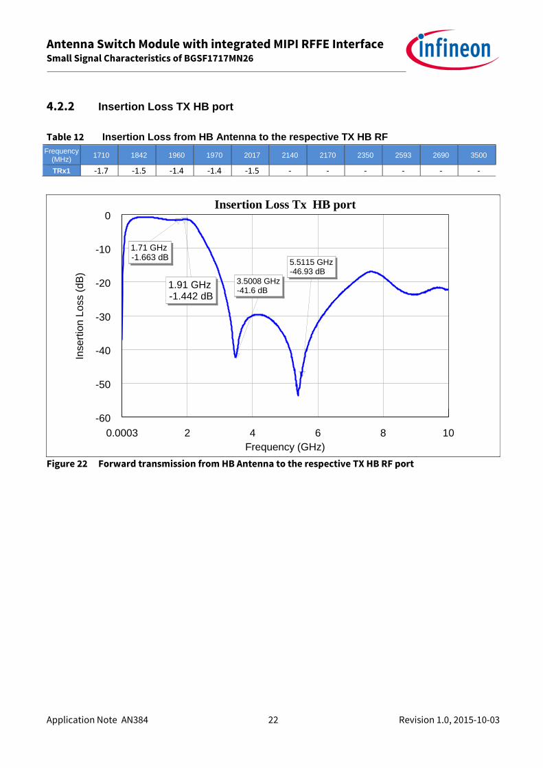
4.2.2 Insertion Loss TX HB port
Figure 22 Forward transmission from HB Antenna to the respective TX HB RF port
0.0003 2 4 6 8 10
Frequency (GHz)
Insertion Loss Tx HB port
-60
-50
-40
-30
-20
-10
0
Inse
rtio
n L
oss (
dB
)
5.5115 GHz-46.93 dB
3.5008 GHz-41.6 dB
1.91 GHz-1.442 dB
1.71 GHz-1.663 dB
Table 12 Insertion Loss from HB Antenna to the respective TX HB RF
Frequency (MHz)
1710 1842 1960 1970 2017 2140 2170 2350 2593 2690 3500
TRx1 -1.7 -1.5 -1.4 -1.4 -1.5 - - - - - -

Antenna Switch Module with integrated MIPI RFFE Interface Small Signal Characteristics of BGSF1717MN26
Application Note AN384 23 Revision 1.0, 2015-10-03
4.2.3 Return Loss from HB Antenna to the respective TRX HB RF Port
Table 13 Return Loss from HB Antenna to the respective TRX HB RF port
Frequency (MHz)
1710 1842 1960 1970 2017 2140 2170 2350 2593 2690 3500
TRx1 -27.8 -20 -16.6 -16.5 -15.6 -14.2 -14 -13.5 -15 -16.6 -15.6
TRx2 -24.3 -18.1 -15.3 -15.2 -14.5 -13.2 -13 -12.7 -14.1 -15.6 -20.3
TRx3 -23.4 -17.2 -14.3 -14.2 -13.4 -12 -11.7 -11.1 -12 -13.1 -23.4
TRx4 -21.4 -15.7 -12.6 -12.5 -11.6 -10 -10 -10 -10 -10 -19.4
TRx5 -19.5 -15.3 -13.1 -13 -12.4 -11.1 -10.9 -10.2 -10.5 -11 -19.5
TRx6 -17.5 -14 -12 -11.9 -11.3 -10.2 -10 -10 -10 -10 -14.9
Figure 23 Return Loss from HB Antenna to the respective TRX HB RF port
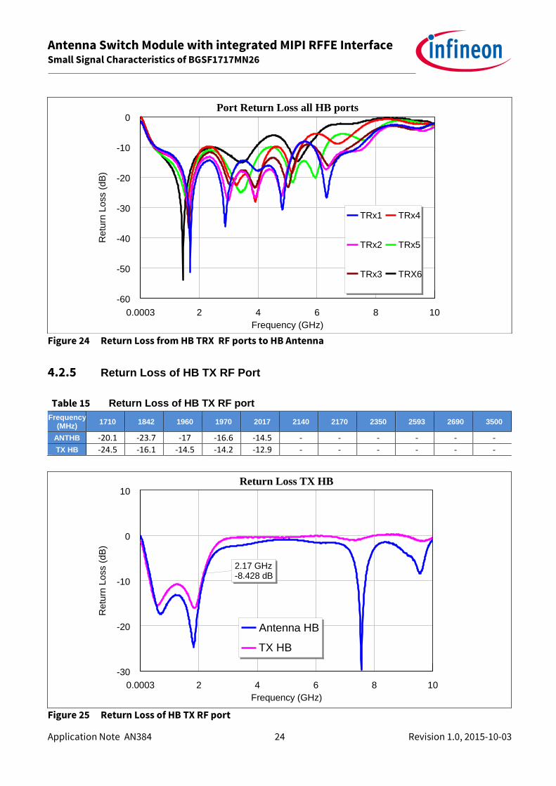
4.2.4 Return Loss of HB TRX RF Ports
Table 14 Return Loss from HB TRX RF ports to HB Antenna
Frequency (MHz)
1710 1842 1960 1970 2017 2140 2170 2350 2593 2690 3500
TRx1 -40.6 -22.7 -18.3 -18.1 -17.1 -15.5 -15.2 -14.4 -17.4 -20.2 -14.5
TRx2 -25.8 -19.4 -16.4 -16.2 -15.4 -14.2 -13.9 -13.3 -15.6 -17.5 -18.2
TRx3 -27.5 -19.1 -15.6 -15.4 -14.5 -13 -12.6 -11.7 -13.1 -14.4 -17.7
TRx4 -24.6 -17 -13.4 -13.1 -12.2 -10.4 -10 -10 -10 -10 -13.1
TRx5 -20.5 -16.4 -14 -13.9 -13.3 -12.1 -11.8 -11 -11.8 -12.5 -24.4
TRx6 -18.2 -14.7 -12.6 -12.5 -11.9 -10.8 -10.5 -10 -10.2 -10.7 -18.1
0.0003 2 4 6 8 10
Frequency (GHz)
ANT Return Loss all HB ports
-60
-50
-40
-30
-20
-10
0
Re
turn
Lo
ss (
dB
)
TRx1
TRx2
TRx3
TRx4
TRx5
Trx6
Antenna Switch Module with integrated MIPI RFFE Interface Small Signal Characteristics of BGSF1717MN26
Application Note AN384 24 Revision 1.0, 2015-10-03
Figure 24 Return Loss from HB TRX RF ports to HB Antenna
4.2.5 Return Loss of HB TX RF Port
Table 15 Return Loss of HB TX RF port
Frequency (MHz)
1710 1842 1960 1970 2017 2140 2170 2350 2593 2690 3500
ANTHB -20.1 -23.7 -17 -16.6 -14.5 - - - - - -
TX HB -24.5 -16.1 -14.5 -14.2 -12.9 - - - - - -
Figure 25 Return Loss of HB TX RF port
0.0003 2 4 6 8 10
Frequency (GHz)
Return Loss TX HB
-30
-20
-10
0
10
Re
turn
Lo
ss (
dB
)
2.17 GHz-8.428 dB
Antenna HB
TX HB
0.0003 2 4 6 8 10
Frequency (GHz)
Port Return Loss all HB ports
-60
-50
-40
-30
-20
-10
0
Re
turn
Lo
ss (
dB
)
TRx1
TRx2
TRx3
TRx4
TRx5
TRX6
Antenna Switch Module with integrated MIPI RFFE Interface Small Signal Characteristics of BGSF1717MN26
Application Note AN384 25 Revision 1.0, 2015-10-03
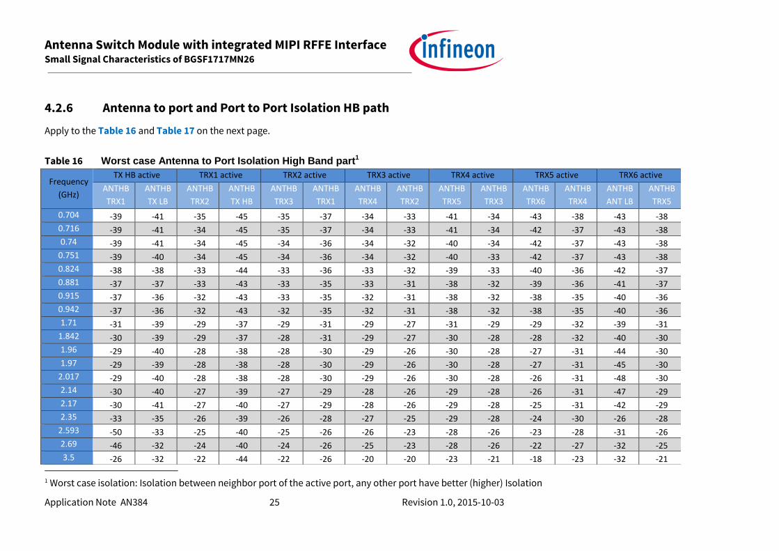
4.2.6 Antenna to port and Port to Port Isolation HB path
Apply to the Table 16 and Table 17 on the next page.
1 Worst case isolation: Isolation between neighbor port of the active port, any other port have better (higher) Isolation
Table 16 Worst case Antenna to Port Isolation High Band part1
Frequency
(GHz)
TX HB active TRX1 active TRX2 active TRX3 active TRX4 active TRX5 active TRX6 active
ANTHB
TRX1
ANTHB
TX LB
ANTHB
TRX2
ANTHB
TX HB
ANTHB
TRX3
ANTHB
TRX1
ANTHB
TRX4
ANTHB
TRX2
ANTHB
TRX5
ANTHB
TRX3
ANTHB
TRX6
ANTHB
TRX4
ANTHB
ANT LB
ANTHB
TRX5
0.704 -39 -41 -35 -45 -35 -37 -34 -33 -41 -34 -43 -38 -43 -38
0.716 -39 -41 -34 -45 -35 -37 -34 -33 -41 -34 -42 -37 -43 -38
0.74 -39 -41 -34 -45 -34 -36 -34 -32 -40 -34 -42 -37 -43 -38
0.751 -39 -40 -34 -45 -34 -36 -34 -32 -40 -33 -42 -37 -43 -38
0.824 -38 -38 -33 -44 -33 -36 -33 -32 -39 -33 -40 -36 -42 -37
0.881 -37 -37 -33 -43 -33 -35 -33 -31 -38 -32 -39 -36 -41 -37
0.915 -37 -36 -32 -43 -33 -35 -32 -31 -38 -32 -38 -35 -40 -36
0.942 -37 -36 -32 -43 -32 -35 -32 -31 -38 -32 -38 -35 -40 -36
1.71 -31 -39 -29 -37 -29 -31 -29 -27 -31 -29 -29 -32 -39 -31
1.842 -30 -39 -29 -37 -28 -31 -29 -27 -30 -28 -28 -32 -40 -30
1.96 -29 -40 -28 -38 -28 -30 -29 -26 -30 -28 -27 -31 -44 -30
1.97 -29 -39 -28 -38 -28 -30 -29 -26 -30 -28 -27 -31 -45 -30
2.017 -29 -40 -28 -38 -28 -30 -29 -26 -30 -28 -26 -31 -48 -30
2.14 -30 -40 -27 -39 -27 -29 -28 -26 -29 -28 -26 -31 -47 -29
2.17 -30 -41 -27 -40 -27 -29 -28 -26 -29 -28 -25 -31 -42 -29
2.35 -33 -35 -26 -39 -26 -28 -27 -25 -29 -28 -24 -30 -26 -28
2.593 -50 -33 -25 -40 -25 -26 -26 -23 -28 -26 -23 -28 -31 -26
2.69 -46 -32 -24 -40 -24 -26 -25 -23 -28 -26 -22 -27 -32 -25
3.5 -26 -32 -22 -44 -22 -26 -20 -20 -23 -21 -18 -23 -32 -21

Antenna Switch Module with integrated MIPI RFFE Interface Small Signal Characteristics of BGSF1717MN26
Application Note AN384 26 Revision 1.0, 2015-10-03
Table 17 Worst case Port to Port Isolation High Band part1
Frequency
(GHz)
TX HB active TRX1 active TRX2 active TRX3 active TRX4 active TRX5 active TRX6 active
TX HB
TRX1
TX HB
TX LB
TRX1
TRX2
TRX1
TX HB
TRX2
TRX3
TRX2
TRX1
TRX3
TRX4
TRX3
TRX2
TRX4
TRX5
TRX4
TRX3
TRX5
TRX6
TRX5
TRX4
TRX6 ANT
LB
TRX6
TRX5
0.704 -37.3 -34 -33.1 -39.3 -33.2 -35 -32.9 -31.6 -38.8 -32.9 -41.5 -35.6 -49.1 -36.1
0.716 -37.2 -33.8 -32.9 -39.2 -33 -35 -32.7 -31.5 -38.7 -32.7 -41.4 -35.4 -49.1 -36.1
0.74 -36.9 -33.6 -32.6 -39.1 -32.7 -34.7 -32.6 -31.2 -38.4 -32.6 -41.1 -35.2 -48.8 -36.1
0.751 -37 -33.6 -32.6 -38.9 -32.6 -34.5 -32.5 -31.2 -38.2 -32.4 -40.8 -34.9 -47.6 -35.5
0.824 -36.3 -33 -32 -38.1 -32 -34 -31.8 -30.6 -37.2 -31.8 -39.5 -34.5 -46.6 -34.9
0.881 -35.8 -32.5 -31.5 -37.6 -31.5 -33.5 -31.3 -30.1 -36.6 -31.4 -38.4 -33.9 -44.9 -34.6
0.915 -35.4 -32.3 -31.3 -37.3 -31.2 -33.2 -31.2 -29.9 -36.3 -31.1 -37.9 -33.7 -44.1 -34.1
0.942 -35.3 -32 -31.2 -37 -31 -33 -30.9 -29.7 -36 -30.8 -37.4 -33.4 -43.4 -34
1.71 -30.3 -38.5 -25.8 -31.3 -25.3 -27.3 -26 -24.2 -28.4 -25.3 -28 -28.1 -41.7 -27.3
1.842 -29.3 -38.6 -24.8 -31.6 -24.4 -26.5 -25.1 -23.2 -27.5 -24.4 -27 -27.3 -42.8 -26.3
1.96 -28.5 -38.2 -24.1 -32.3 -23.6 -25.6 -24.4 -22.4 -26.8 -23.7 -26.1 -26.6 -46.2 -25.4
1.97 -28.5 -38.4 -24 -32.3 -23.5 -25.5 -24.4 -22.3 -26.7 -23.6 -26 -26.4 -47.2 -25.3
2.017 -28.3 -38.6 -23.7 -32.8 -23.2 -25.2 -24.1 -22 -26.4 -23.3 -25.7 -26.2 -50.9 -24.9
2.14 -28.4 -38.7 -22.9 -33.9 -22.3 -24.4 -23.3 -21.2 -25.6 -22.5 -24.9 -25.4 -49.8 -24.1
2.17 -28.6 -38.6 -22.7 -34.3 -22.2 -24.2 -23.1 -21 -25.6 -22.4 -24.8 -25.2 -44.6 -23.9
2.35 -31 -35.6 -21.7 -37.4 -21.1 -23.3 -21.9 -20 -24.7 -21.3 -23.8 -24 -28.4 -22.7
2.593 -35.5 -35.5 -20.4 -39.1 -19.8 -21.9 -20.3 -18.6 -23.6 -19.9 -22.4 -22.4 -33.1 -21.5
2.69 -38.1 -35.3 -19.9 -39.9 -19.4 -21.5 -19.6 -18.2 -23.2 -19.4 -22 -21.8 -34.4 -21
3.5 -42.7 -31.1 -19.6 -45.6 -18.5 -20.9 -17.7 -17.9 -21.1 -18.4 -18.8 -19.6 -33.3 -18.7
1 Worst case isolation: Isolation between neighbor port of the active port, any other port have better (higher) Isolation
Antenna Switch Module with integrated MIPI RFFE Interface Small Signal Characteristics of BGSF1717MN26
Application Note AN384 27 Revision 1.0, 2015-10-03
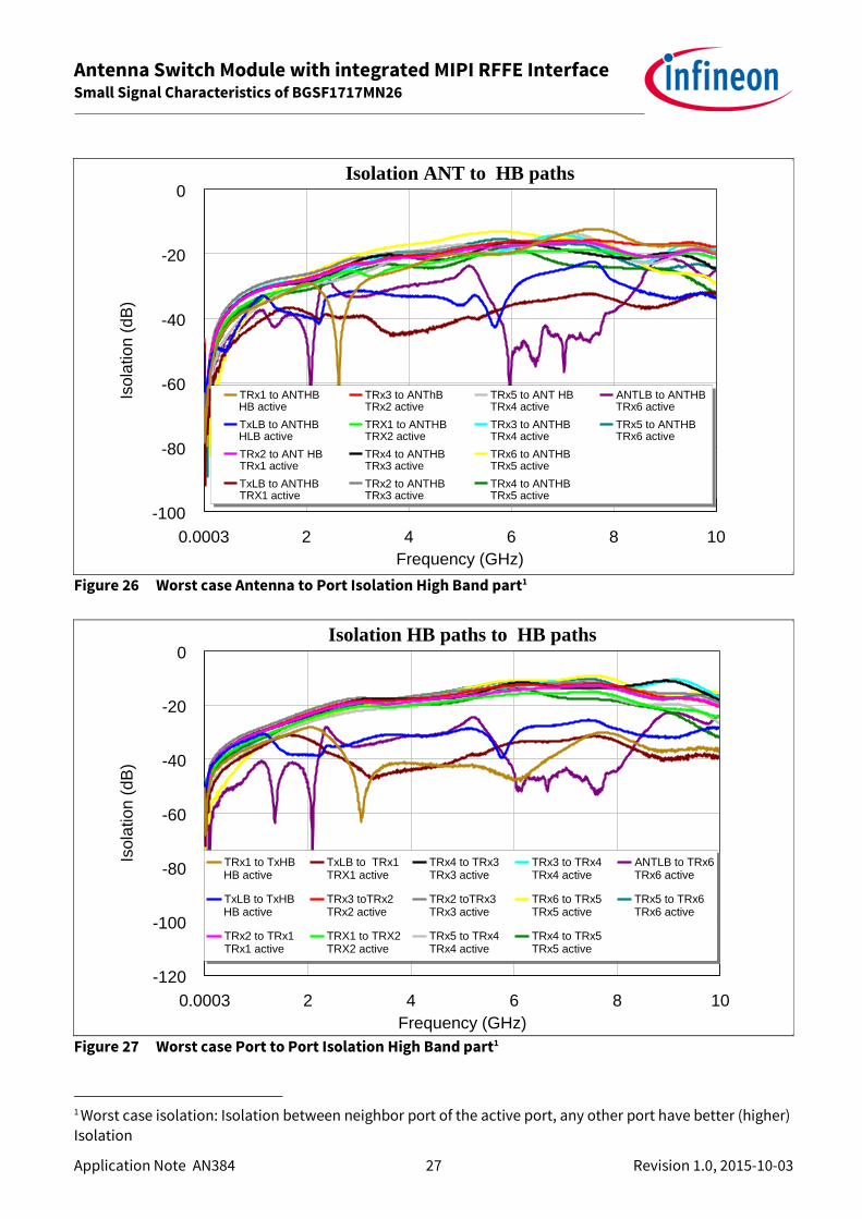
Figure 26 Worst case Antenna to Port Isolation High Band part1
Figure 27 Worst case Port to Port Isolation High Band part1
1 Worst case isolation: Isolation between neighbor port of the active port, any other port have better (higher)
Isolation
0.0003 2 4 6 8 10
Frequency (GHz)
Isolation ANT to HB paths
-100
-80
-60
-40
-20
0
Isola
tion (
dB
)
TRx1 to ANTHBHB active
TxLB to ANTHBHLB active
TRx2 to ANT HBTRx1 active
TxLB to ANTHBTRX1 active
TRx3 to ANThBTRx2 active
TRX1 to ANTHBTRX2 active
TRx4 to ANTHBTRx3 active
TRx2 to ANTHBTRx3 active
TRx5 to ANT HBTRx4 active
TRx3 to ANTHBTRx4 active
TRx6 to ANTHBTRx5 active
TRx4 to ANTHBTRx5 active
ANTLB to ANTHBTRx6 active
TRx5 to ANTHBTRx6 active
0.0003 2 4 6 8 10
Frequency (GHz)
Isolation HB paths to HB paths
-120
-100
-80
-60
-40
-20
0
Iso
latio
n (
dB
)
TRx1 to TxHBHB active
TxLB to TxHBHB active
TRx2 to TRx1TRx1 active
TxLB to TRx1TRX1 active
TRx3 toTRx2TRx2 active
TRX1 to TRX2TRX2 active
TRx4 to TRx3TRx3 active
TRx2 toTRx3TRx3 active
TRx5 to TRx4TRx4 active
TRx3 to TRx4TRx4 active
TRx6 to TRx5TRx5 active
TRx4 to TRx5TRx5 active
ANTLB to TRx6TRx6 active
TRx5 to TRx6TRx6 active

Antenna Switch Module with integrated MIPI RFFE Interface Non-Linear performance of BGSF1717MN26
Application Note AN384 28 Revision 1.0, 2015-10-03
5 Non-Linear performance of BGSF1717MN26
Smart phones today can operate across several cellular bands covering GSM / EDGE / CDMA / UMTS /
WCDMA / LTE/TD-SCDMA / TD-LTE / LTE-A. The design of the RF front-end part in modern cellular phones is
becoming increasingly complex and demanding due to the increasing number of frequency bands and
modes that the phone needs to support. One of the main components of the RF front-end is the antenna
switch that selects which transmitter (TX)/receiver (RX) path can be connected to the antenna. The RF
switch has to satisfy high linearity requirements. The following material describes some of the main
challenges of antenna switches in mobile applications.
Modern smartphones are multi-mode devices that are capable of connecting to 2G, 3G and 4G networks.
These networks often use different frequency bands. The smartphone’s RF frontend must therefore include
band-specific components. In order to appropriately route signals for a given mode and band of operation,
a high-performance RF switch is an essential component of the front-end circuitry. The performance
requirements of the RF switch are discussed in the following sections.
5.1 Intermodulation
Intermodulation Distortion (IMD2 and IMD3) is a parameter that describes the linearity of a device under
multi-tone conditions. The intermodulation between different frequency components generates undesired
output frequencies at the sum and difference frequencies of the input tones, and at multiples of those sum
and difference frequencies. Some of these possible intermodulation scenarios are shown in the Figure 28.
In this example, the transmitted (Tx) signal from the main antenna is coupled into the diversity antenna
with high power. This signal (20 dBm) and a received jammer signal (-15 dBm) are entering the switch.
Certain combinations of the TX and jammer frequencies are producing second- and third-order
intermodulation products that fall into the desired reception band, and reduce the sensitivity of the
receiver.
In Table 18 and Table 20 test conditions Band I and V and the linearity specifications for an undisturbed
communication are given.
Antenna Switch Module with integrated MIPI RFFE Interface Non-Linear performance of BGSF1717MN26
Application Note AN384 29 Revision 1.0, 2015-10-03
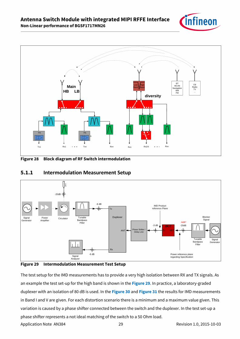
Figure 28 Block diagram of RF Switch intermodulation
5.1.1 Intermodulation Measurement Setup
Figure 29 Intermodulation Measurement Test Setup
The test setup for the IMD measurements has to provide a very high isolation between RX and TX signals. As
an example the test set-up for the high band is shown in the Figure 29. In practice, a laboratory-graded
duplexer with an isolation of 80 dB is used. In the Figure 30 and Figure 31 the results for IMD measurements
in Band I and V are given. For each distortion scenario there is a minimum and a maximum value given. This
variation is caused by a phase shifter connected between the switch and the duplexer. In the test set-up a
phase shifter represents a not ideal matching of the switch to a 50 Ohm load.
Lo
ad
Signal
Generator
Power
AmplifierCirculator
-20dB
Signal
Analyzer
-6 dB
-6 dB
Duplexer
Tx
Rx
ANTPhase Shifter /
Delay Line
Signal
Generator
DUT -20dB
Power reference plane
regarding Specification
Tx ANT
Tunable
Bandpass
Filter-3 dB
Tunable
Bandpass
Filter
Blocker
Signal
IMD Product
reference Plane
-6dB*
PA
PA
PA
Tx1 Rx1 Txn Rxn Rx1 Rx2/3 Rxn
BT
WLAN
Navigation
Wifi
FM
Low
Band
High
BandMain
HB LBdiversity
CB
Radio
TV
...

Antenna Switch Module with integrated MIPI RFFE Interface Non-Linear performance of BGSF1717MN26
Application Note AN384 30 Revision 1.0, 2015-10-03
5.1.2 Intermodulation Measurement conditions for Band I
Table 18 Test conditions and specifications of IMD measurements
Band 1
TX Interferer IMD product
Test case FIN (MHz) PIN (dBm) CW FIN (MHz) PIN (dBm) CW FIMD (MHz)
IMD3
1950 20
1760
-15 2140 IMD2 low 190
IMD2 high 4090
5.1.3 Intermodulation Measurement Results for Band I
IMD Band I IMD Test Set-up One (left)
Tx 1950 MHz PBL = -15 dBm
Rx 2140 MHz
T = 25°C BGSF1717MN26
IMD2Low ANT_HB - TRX1 ANT_HB – TX_HB
Blocker Vdd Min Max Min Max
fb = 190 MHz PTX = 20 dBm
3,3 -110,7 -101,2 -109,66 -102,6
IMD2High ANT_HB - TRX1 ANT_HB - TX_HB
Blocker Vdd Min Max Min Max
fb = 4090 MHz PTX = 20 dBm
3,3 -119,5 -115,8 -132,1 -123,4
IMD3 ANT_HB - TRX1 ANT_HB - TX_HB
Blocker Vdd Min Max Min Max
fb = 1760 MHz PTX = 20 dBm
3,3 -131,0 -127,8 -132,1 -121,7
Figure 30 Intermodulation measurement results for Band I
Table 19 Typical and maximal value of intermodulation products in dBm for Band I
IMD2 Low IMD2 High IMD3
Typ. Max. Typ. Max. Typ. Max.
-106,0 -101,2 -122,7 -115,8 -128,2 -121,7
Antenna Switch Module with integrated MIPI RFFE Interface Non-Linear performance of BGSF1717MN26
Application Note AN384 31 Revision 1.0, 2015-10-03
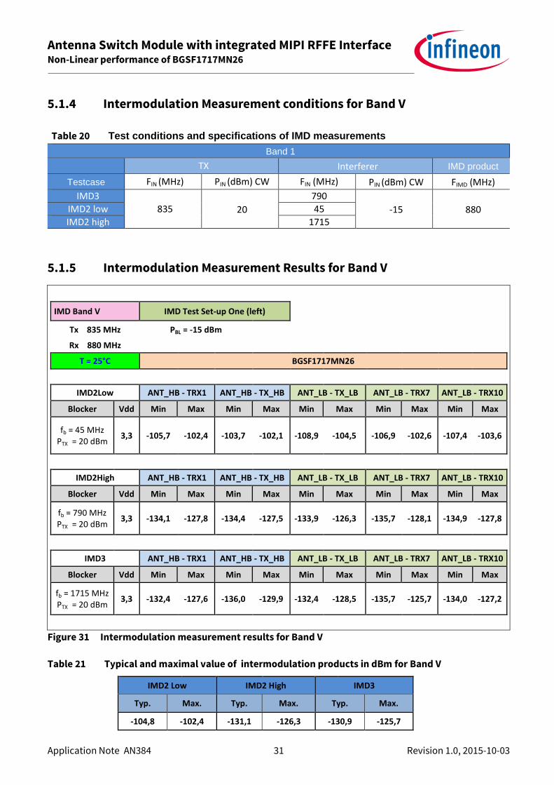
5.1.4 Intermodulation Measurement conditions for Band V
Table 20 Test conditions and specifications of IMD measurements
Band 1
TX Interferer IMD product
Testcase FIN (MHz) PIN (dBm) CW FIN (MHz) PIN (dBm) CW FIMD (MHz)
IMD3
835 20
790
-15 880 IMD2 low 45
IMD2 high 1715
5.1.5 Intermodulation Measurement Results for Band V
IMD Band V IMD Test Set-up One (left)
Tx 835 MHz PBL = -15 dBm
Rx 880 MHz
T = 25°C BGSF1717MN26
IMD2Low ANT_HB - TRX1 ANT_HB - TX_HB ANT_LB - TX_LB ANT_LB - TRX7 ANT_LB - TRX10
Blocker Vdd Min Max Min Max Min Max Min Max Min Max
fb = 45 MHz PTX = 20 dBm
3,3 -105,7 -102,4 -103,7 -102,1 -108,9 -104,5 -106,9 -102,6 -107,4 -103,6
IMD2High ANT_HB - TRX1 ANT_HB - TX_HB ANT_LB - TX_LB ANT_LB - TRX7 ANT_LB - TRX10
Blocker Vdd Min Max Min Max Min Max Min Max Min Max
fb = 790 MHz PTX = 20 dBm
3,3 -134,1 -127,8 -134,4 -127,5 -133,9 -126,3 -135,7 -128,1 -134,9 -127,8
IMD3 ANT_HB - TRX1 ANT_HB - TX_HB ANT_LB - TX_LB ANT_LB - TRX7 ANT_LB - TRX10
Blocker Vdd Min Max Min Max Min Max Min Max Min Max
fb = 1715 MHz PTX = 20 dBm
3,3 -132,4 -127,6 -136,0 -129,9 -132,4 -128,5 -135,7 -125,7 -134,0 -127,2
Figure 31 Intermodulation measurement results for Band V
Table 21 Typical and maximal value of intermodulation products in dBm for Band V
IMD2 Low IMD2 High IMD3
Typ. Max. Typ. Max. Typ. Max.
-104,8 -102,4 -131,1 -126,3 -130,9 -125,7

Antenna Switch Module with integrated MIPI RFFE Interface Non-Linear performance of BGSF1717MN26
Application Note AN384 32 Revision 1.0, 2015-10-03
5.2 Harmonic Distortion
Harmonic distortion is another important parameter for the characterization of an RF switch. RF switches
have to withstand high RF levels, up to 36 dBm. This high RF power at the input of a switch generates
harmonics of the waveform that is present. These harmonics (2nd and 3rd) can interfere with other reception
bands or can cause distortion in other RF applications (GPS, WLan) within the mobile phone.
Figure 32 Harmonic Generation Measurement setup
5.2.1 Harmonic Generation Measurement conditions
Table 22 Harmonic Generation measurement Conditions
Tx Harmonic Products
FIN (MHz) PIN (dBm), 50% DC FH2(MHz) FH3 (MHz)
824 20…36 TX LB port
1648 2472 20…27 TRX LB ports
1800 20…36 TX HB port
3600 3600 20…27 TRX HB ports
The result for the harmonic generation at 824 MHZ and 1800 MHz is shown in the Figure 33 and Figure 35.
The input power (Pin) is plotted on the X-Axis, and the generated harmonic amplitude is given in dBm on the
Y-Axis.
Lo
ad
Signal
Generator
Power
AmplifierCirculator
F = Ffundamantel
Lowpass Filter
Ffilter ≥ Ffundamental
-20dB
Directional
Coupler
Directional
CouplerSignal
Analyzer
-3dBPower meter
A
B
-20dB
-10dB
DUTTx ANT
-3 dB
-3 dB
Highpass Filter
Ffundamental << Ffilter ≤ Fharmonics
reference plane
Pin (Ffundamental)
reference plane
Pout (Fharmonic and
Ffundamental)
measurement
Pin (Ffundamental)
measurement
Pout (Ffundamental)
Antenna Switch Module with integrated MIPI RFFE Interface Non-Linear performance of BGSF1717MN26
Application Note AN384 33 Revision 1.0, 2015-10-03
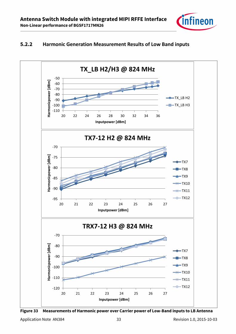
5.2.2 Harmonic Generation Measurement Results of Low Band inputs
Figure 33 Measurements of Harmonic power over Carrier power of Low-Band inputs to LB Antenna
-110
-100
-90
-80
-70
-60
-50
20 22 24 26 28 30 32 34 36Har
mo
nic
po
we
r [d
Bm
]
Inputpower [dBm]
TX_LB H2/H3 @ 824 MHz
TX_LB H2
TX_LB H3
-95
-90
-85
-80
-75
-70
20 21 22 23 24 25 26 27
Har
mo
nic
po
we
r [d
Bm
]
Inputpower [dBm]
TX7-12 H2 @ 824 MHz
TX7
TX8
TX9
TX10
TX11
TX12
-120
-110
-100
-90
-80
-70
20 21 22 23 24 25 26 27
Har
mo
nic
po
we
r [d
Bm
]
Inputpower [dBm]
TRX7-12 H3 @ 824 MHz
TX7
TX8
TX9
TX10
TX11
TX12

Antenna Switch Module with integrated MIPI RFFE Interface Non-Linear performance of BGSF1717MN26
Application Note AN384 34 Revision 1.0, 2015-10-03
Figure 34 Harmonic power measurements of high linear LB input TRX10 over the Band 17 carrier
In Figure 34 the generated harmonic power of a very high linear input TX10 is shown measured at the operating frequency of Band 17 FDD (710 MHz). The spacing between the carrier frequency and the
generated harmonic at the maximum operated power sets up to 98 dBc for H2 and 133 dBc for H3. This is an outstanding performance among other competitors.
-125
-115
-105
-95
-85
-75
-65
20 22 24 26
Har
mo
nic
po
we
r [d
Bm
]
Inputpower [dBm]
TX10 H2/H3 @ (Band 17 FDD) 710 MHz
H2
H3
Antenna Switch Module with integrated MIPI RFFE Interface Non-Linear performance of BGSF1717MN26
Application Note AN384 35 Revision 1.0, 2015-10-03
5.2.3 Harmonic Generation Measurement Results of High Band inputs
Figure 35 Measurements of Harmonic power over Carrier power of High-Band inputs to HB Antenna
-125
-115
-105
-95
-85
-75
-65
20 22 24 26 28 30 32 34 36
Har
mo
nic
po
we
r [d
Bm
]
Inputpower [dBm]
TX_HB H3 @ 1800 MHz
TX_HB H3
TX_HB H2
-110
-105
-100
-95
-90
-85
-80
20 21 22 23 24 25 26 27
Har
mo
nic
po
we
r [d
Bm
]
Inputpower [dBm]
TRX1-6 H2 @ 1800 MHz
TX1
TX2
TX3
TX4
TX5
TX6
-110
-105
-100
-95
-90
-85
-80
-75
-70
20 21 22 23 24 25 26 27
Har
mo
nic
po
we
r [d
Bm
]
Inputpower [dBm]
TRX1-6 H3 @ 1800 MHz
TX1
TX2
TX3
TX4
TX5
TX6
Antenna Switch Module with integrated MIPI RFFE Interface Switching time
Application Note AN384 36 Revision 1.0, 2015-10-03
6 Switching time
Table 23 Switching time values
Parameter Symbol Values Unit Note / Test Conditions
Min. Typ. Max.
Switching Time
On/Off ton/off - 1 - µs 10% ON to 90% ON; 90% OFF to 10% OFF
Boost Converter
Settling Time
tBC - - 25 µs After power down mode
For a “switching time” measurement a signal generator and a digital oscilloscope is used. A 100 MHz continuous sine signal with 0 dBm signal level was switched to all LB and HB inputs one after another. The
output of the switch connected from one side either to HB Antenna or to LB Antenna and from the other side to a digital oscilloscope. Typical time required to raise the signal power from 10% ON Mode up to 90 % ON of
the Signal Level lies by 1 µs. In the Figure 36 the switching time of the TX_LB input is shown. Maximum time required between switch power-up till being able to switch to desired RF-path is 25 µs.
Figure 36 Switching time measurements of the TX_LB input to the LB Antenna

Antenna Switch Module with integrated MIPI RFFE Interface Appendix: Switch Controller Unit
Application Note AN384 37 Revision 1.0, 2015-10-03
7 Appendix: Switch Controller Unit
The BGSF1717MN26 is controlled via MIPI interface and Infineon offers a MIPI-Controller unit to ease the
evaluation of its BGSF1717MN26 on application board. The unit is very simple to use with a few buttons to
select the right device and different states. This section helps as a short user guide for the controller unit
shown in Figure 37. The controller unit requires a DC supply of 5.5V with a current capability of ~50mA.
Figure 37 Switch Controller Unit Board
7.1 Operating Guide
Please observe the following steps to use the controller unit:
1. Connect evaluation board and control unit via controller cable
2. Connect control unit to power supply
3. Press P1 and P3 simultaneously until desired switch type is displayed
- “77” for BGSF1717MN26
4. Press P1 or P3 to enable active mode “PU” is displayed*
5. Press P1 or P3 to alter switch state
- IS … Isolation Mode (all channels off)
- PD … Power Down Mode (low current consumption)
- PU ... Power Up Mode (active mode)
- T1 – TC and LB, HB ... TRX1 – TRX12 and TX LB and TXHB are enabled
P3
P2
P1
to BGSF18D
G V G
N C N
D C D
GND GND
GND GND
Vcc NC
LVdd SPI
FRM CLK
I/F Cable to BGSF1717MN26

Antenna Switch Module with integrated MIPI RFFE Interface Appendix: Switch Controller Unit
Application Note AN384 38 Revision 1.0, 2015-10-03
7.2 Display Settings of the Controller Unit
Table 24 Setting Display of Active RF Path, Power UP, Power Down and Isolation State
LED Display State of BGSF1717MN26
T1 TRX1
T2 TRX2
T3 TRX3
T4 TRX4
T5 TRX5
T6 TRX6
T7 TRX7
T8 TRX8
T9 TRX9
TA TRX10
TB TRX11
TC TRX12
LB TX LB
HB TX LB
IS Isolation State
PU Power Up State
PD Power Down State

Antenna Switch Module with integrated MIPI RFFE Interface Authors
Application Note AN384 39 Revision 1.0, 2015-10-03
8 Authors Andre Dewai, Senior Application Engineer of the Business Unit “RF and Sensors”
Sergey Karpov, Application Engineer of the Business Unit “RF and Sensors”

Antenna Switch Module with integrated MIPI RFFE Interface Authors
Application Note AN384 40 Revision 1.0, 2015-10-03
Remark 1) The graphs are generated with the simulation program AWR Microwave Office®.
Revision History
Major changes since the last revision
Page or Reference Description of change
This is 1st
version (Rev. 1.0)

Published by
Infineon Technologies AG
81726 Munich, Germany
© 2016 Infineon Technologies AG. All Rights Reserved.
Do you have a question about any
aspect of this document?
Email: [email protected]
Document reference
Legal Disclaimer THE INFORMATION GIVEN IN THIS APPLICATION NOTE (INCLUDING BUT NOT LIMITED TO CONTENTS OF REFERENCED WEBSITES) IS GIVEN AS A HINT FOR THE IMPLEMENTATION OF THE INFINEON TECHNOLOGIES COMPONENT ONLY AND SHALL NOT BE REGARDED AS ANY DESCRIPTION OR WARRANTY OF A CERTAIN FUNCTIONALITY, CONDITION OR QUALITY OF THE INFINEON TECHNOLOGIES COMPONENT. THE RECIPIENT OF THIS APPLICATION NOTE MUST VERIFY ANY FUNCTION DESCRIBED HEREIN IN THE REAL APPLICATION. INFINEON TECHNOLOGIES HEREBY DISCLAIMS ANY AND ALL WARRANTIES AND LIABILITIES OF ANY KIND (INCLUDING WITHOUT LIMITATION WARRANTIES OF NON-INFRINGEMENT OF INTELLECTUAL PROPERTY RIGHTS OF ANY THIRD PARTY) WITH RESPECT TO ANY AND ALL INFORMATION GIVEN IN THIS APPLICATION NOTE.
Information For further information on technology, delivery terms and conditions and prices, please contact the nearest Infineon Technologies Office (www.infineon.com).
Warnings Due to technical requirements, components may contain dangerous substances. For information on the types in question, please contact the nearest Infineon Technologies Office. Infineon Technologies components may be used in life-support devices or systems only with the express written approval of Infineon Technologies, if a failure of such components can reasonably be expected to cause the failure of that life-support device or system or to affect the safety or effectiveness of that device or system. Life support devices or systems are intended to be implanted in the human body or to support and/or maintain and sustain and/or protect human life. If they fail, it is reasonable to assume that the health of the user or other persons may be endangered.
www.infineon.com
Trademarks of Infineon Technologies AG AURIX™, C166™, CanPAK™, CIPOS™, CIPURSE™, CoolGaN™, CoolMOS™, CoolSET™, CoolSiC™, CORECONTROL™, CROSSAVE™, DAVE™, DI-POL™, DrBLADE™, EasyPIM™, EconoBRIDGE™, EconoDUAL™, EconoPACK™, EconoPIM™, EiceDRIVER™, eupec™, FCOS™, HITFET™, HybridPACK™, ISOFACE™, IsoPACK™, i-Wafer™, MIPAQ™, ModSTACK™, my-d™, NovalithIC™, OmniTune™, OPTIGA™, OptiMOS™, ORIGA™, POWERCODE™, PRIMARION™, PrimePACK™, PrimeSTACK™, PROFET™, PRO-SIL™, RASIC™, REAL3™, ReverSave™, SatRIC™, SIEGET™, SIPMOS™, SmartLEWIS™, SOLID FLASH™, SPOC™, TEMPFET™, thinQ!™, TRENCHSTOP™, TriCore™.
Other Trademarks Advance Design System™ (ADS) of Agilent Technologies, AMBA™, ARM™, MULTI-ICE™, KEIL™, PRIMECELL™, REALVIEW™, THUMB™, µVision™ of ARM Limited, UK. ANSI™ of American National Standards Institute. AUTOSAR™ of AUTOSAR development partnership. Bluetooth™ of Bluetooth SIG Inc. CAT-iq™ of DECT Forum. COLOSSUS™, FirstGPS™ of Trimble Navigation Ltd. EMV™ of EMVCo, LLC (Visa Holdings Inc.). EPCOS™ of Epcos AG. FLEXGO™ of Microsoft Corporation. HYPERTERMINAL™ of Hilgraeve Incorporated. MCS™ of Intel Corp. IEC™ of Commission Electrotechnique Internationale. IrDA™ of Infrared Data Association Corporation. ISO™ of INTERNATIONAL ORGANIZATION FOR STANDARDIZATION. MATLAB™ of MathWorks, Inc. MAXIM™ of Maxim Integrated Products, Inc. MICROTEC™, NUCLEUS™ of Mentor Graphics Corporation. MIPI™ of MIPI Alliance, Inc. MIPS™ of MIPS Technologies, Inc., USA. muRata™ of MURATA MANUFACTURING CO., MICROWAVE OFFICE™ (MWO) of Applied Wave Research Inc., OmniVision™ of OmniVision Technologies, Inc. Openwave™ of Openwave Systems Inc. RED HAT™ of Red Hat, Inc. RFMD™ of RF Micro Devices, Inc. SIRIUS™ of Sirius Satellite Radio Inc. SOLARIS™ of Sun Microsystems, Inc. SPANSION™ of Spansion LLC Ltd. Symbian™ of Symbian Software Limited. TAIYO YUDEN™ of Taiyo Yuden Co. TEAKLITE™ of CEVA, Inc. TEKTRONIX™ of Tektronix Inc. TOKO™ of TOKO KABUSHIKI KAISHA TA. UNIX™ of X/Open Company Limited. VERILOG™, PALLADIUM™ of Cadence Design Systems, Inc. VLYNQ™ of Texas Instruments Incorporated. VXWORKS™, WIND RIVER™ of WIND RIVER SYSTEMS, INC. ZETEX™ of Diodes Zetex Limited. Last Trademarks Update 2014-07-17
Edition 2015-10-03
AN_2014_11_PL32_003