ORDER NO. VM1202001CEB27
High Definition Video CameraModel No. HC-V500MP
HC-V500MPCHC-V500MPUHC-V500MEBHC-V500MECHC-V500MEEHC-V500MEGHC-V500MEPHC-V500MGAHC-V500MGCHC-V500MGKHC-V500MGNHC-V500MGTHC-V500PHC-V500PCHC-V500EBHC-V500ECHC-V500EEHC-V500EFHC-V500EGHC-V500EPHC-V500GAHC-V500GCHC-V500GKHC-V500GN
© Panasonic Corporation 2012 Unauthorized copy-ing and distribution is a violation of law.
HC-V500GTColour[HC-V500](K)...........Black Type(S)...........Silver Type (except P/PC/EC/EF/GK/GT)(R)...........Red Type (except P/PC/EB/EE/GN/GT)
[HC-V500M](K)...........Black Type(R)...........Red Type (only GK)
TABLE OF CONTENTSPAGE PAGE
1 Safety Precautions -----------------------------------------------31.1. General Guidelines ----------------------------------------31.2. Leakage Current Cold Check ---------------------------31.3. Leakage Current Hot Check (See Figure 1.)--------3
2 Warning --------------------------------------------------------------42.1. Prevention of Electrostatic Discharge (ESD)
to Electrostatically Sensitive (ES) Devices ----------42.2. How to Recycle the Lithium Ion Battery (U.S.
Only)-----------------------------------------------------------42.3. Caution for AC Cord (For EB/GC) ---------------------52.4. How to Replace the Lithium Battery-------------------6
3 Service Navigation------------------------------------------------73.1. Introduction --------------------------------------------------73.2. General Description About Lead Free Solder
(PbF) ----------------------------------------------------------73.3. Important Notice 1:(Other than U.S.A. and
Canadian Market) ------------------------------------------73.4. How to Define the Model Suffix (NTSC or PAL
model)---------------------------------------------------------83.5. Formatting----------------------------------------------------9
4 Specifications ---------------------------------------------------- 105 Location of Controls and Components------------------ 126 Service Mode ----------------------------------------------------- 16
6.1. Built-in Memory Self Check Execution (HC-V500M only) ----------------------------------------------- 17
6.2. Lock Search History Indication ----------------------- 176.3. Power ON Self Check Result Display--------------- 186.4. Erasing the lock histories ------------------------------ 186.5. Camera data indications while the video
playback ---------------------------------------------------- 197 Service Fixture & Tools --------------------------------------- 20
7.1. When Replacing the Main P.C.B. -------------------- 207.2. Service Position ------------------------------------------ 20
8 Disassembly and Assembly Instructions --------------- 218.1. Disassembly Flow Chart for the Unit ---------------- 218.2. PCB Location---------------------------------------------- 218.3. Disassembly Procedure for the Unit ---------------- 22
9 Measurements and Adjustments -------------------------- 299.1. Electric Adjustment -------------------------------------- 29
10 Factory Setting -------------------------------------------------- 3110.1. How To Turn On The Factory Settings? ----------- 3110.2. What Is The Factory Settings? ----------------------- 32
11 Block Diagram --------------------------------------------------- 3311.1. Overall Block Diagram---------------------------------- 3311.2. Camera/System Control Circuit Block
Diagram ---------------------------------------------------- 3411.3. Video/Audio Signal Process(1) Circuit Block
Diagram ---------------------------------------------------- 3511.4. Video/Audio Signal Process(2) Circuit Block
Diagram ---------------------------------------------------- 3611.5. Lens Drive Circuit Block Diagram ------------------- 3711.6. Power Supply Circuit Block Diagram --------------- 38
12 Wiring Connection Diagram -------------------------------- 3912.1. Interconnection Diagram------------------------------- 39
2
1 Safety Precautions1.1. General Guidelines
1. IMPORTANT SAFETY NOTICEThere are special components used in this equipmentwhich are important for safety. These parts are marked by
in the Schematic Diagrams, Circuit Board Layout,Exploded Views and Replacement Parts List. It is essen-tial that these critical parts should be replaced with manu-facturer’s specified parts to prevent X-RADIATION,shock, fire, or other hazards. Do not modify the originaldesign without permission of manufacturer.
2. An Isolation Transformer should always be used duringthe servicing of AC Adaptor whose chassis is not isolatedfrom the AC power line. Use a transformer of adequatepower rating as this protects the technician from acci-dents resulting in personal injury from electrical shocks. Itwill also protect AC Adaptor from being damaged by acci-dental shorting that may occur during servicing.
3. When servicing, observe the original lead dress. If a shortcircuit is found, replace all parts which have been over-heated or damaged by the short circuit.
4. After servicing, see to it that all the protective devicessuch as insulation barriers, insulation papers shields areproperly installed.
5. After servicing, make the following leakage currentchecks to prevent the customer from being exposed toshock hazards.
1.2. Leakage Current Cold Check1. Unplug the AC cord and connect a jumper between the
two prongs on the plug.2. Measure the resistance value, with an ohmmeter,
between the jumpered AC plug and each exposed metal-lic cabinet part on the equipment such as screwheads,connectors, control shafts, etc. When the exposed metal-lic part has a return path to the chassis, the readingshould be between 1 MΩ and 5.2 MΩ. When the exposedmetal does not have a return path to the chassis, thereading must be infinity.
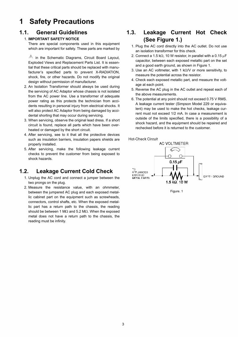
1.3. Leakage Current Hot Check(See Figure 1.)
1. Plug the AC cord directly into the AC outlet. Do not usean isolation transformer for this check.
2. Connect a 1.5 kΩ, 10 W resistor, in parallel with a 0.15 μFcapacitor, between each exposed metallic part on the setand a good earth ground, as shown in Figure 1.
3. Use an AC voltmeter, with 1 kΩ/V or more sensitivity, tomeasure the potential across the resistor.
4. Check each exposed metallic part, and measure the volt-age at each point.
5. Reverse the AC plug in the AC outlet and repeat each ofthe above measurements.
6. The potential at any point should not exceed 0.75 V RMS.A leakage current tester (Simpson Model 229 or equiva-lent) may be used to make the hot checks, leakage cur-rent must not exceed 1/2 mA. In case a measurement isoutside of the limits specified, there is a possibility of ashock hazard, and the equipment should be repaired andrechecked before it is returned to the customer.
Figure. 1
3
2 Warning2.1. Prevention of Electrostatic Discharge (ESD) to Electrostatically
Sensitive (ES) DevicesSome semiconductor (solid state) devices can be damaged easily by static electricity. Such components commonly are called Elec-trostatically Sensitive (ES) Devices. Examples of typical ES devices are integrated circuits and some field-effect transistors andsemiconductor "chip" components. The following techniques should be used to help reduce the incidence of component damagecaused by electrostatic discharge (ESD).
1. Immediately before handling any semiconductor component or semiconductor-equipped assembly, drain off any ESD on yourbody by touching a known earth ground. Alternatively, obtain and wear a commercially available discharging ESD wrist strap,which should be removed for potential shock reasons prior to applying power to the unit under test.
2. After removing an electrical assembly equipped with ES devices, place the assembly on a conductive surface such as alumi-num foil, to prevent electrostatic charge buildup or exposure of the assembly.
3. Use only a grounded-tip soldering iron to solder or unsolder ES devices.4. Use only an antistatic solder removal device. Some solder removal devices not classified as "antistatic (ESD protected)" can
generate electrical charge sufficient to damage ES devices.5. Do not use freon-propelled chemicals. These can generate electrical charges sufficient to damage ES devices.6. Do not remove a replacement ES device from its protective package until immediately before you are ready to install it. (Most
replacement ES devices are packaged with leads electrically shorted together by conductive foam, aluminum foil or compara-ble conductive material).
7. Immediately before removing the protective material from the leads of a replacement ES device, touch the protective materialto the chassis or circuit assembly into which the device will be installed.CAUTION :
Be sure no power is applied to the chassis or circuit, and observe all other safety precautions.8. Minimize bodily motions when handling unpackaged replacement ES devices. (Otherwise harmless motion such as the
brushing together of your clothes fabric or the lifting of your foot from a carpeted floor can generate static electricity (ESD) suf-ficient to damage an ES device).
2.2. How to Recycle the Lithium Ion Battery (U.S. Only)
4

2.3. Caution for AC Cord (For EB/GC)
2.3.1. Information for Your SafetyIMPORTANT
Your attention is drawn to the fact that recording of pre-recorded tapes or discs or other published or broadcastmaterial may infringe copyright laws.
WARNINGTo reduce the risk of fire or shock hazard, do not exposethis equipment to rain or moisture.
CAUTIONTo reduce the risk of fire or shock hazard and annoyinginterference, use the recommended accessories only.
FOR YOUR SAFETY DO NOT REMOVE THE OUTER COVERTo prevent electric shock, do not remove the cover. No userserviceable parts inside. Refer servicing to qualified servicepersonnel.
2.3.2. Caution for AC Mains LeadFor your safety, please read the following text carefully.
This appliance is supplied with a moulded three-pin mains plugfor your safety and convenience.A 5-ampere fuse is fitted in this plug.Should the fuse need to be replaced please ensure that thereplacement fuse has a rating of 5 amperes and it is approvedby ASTA or BSI to BS1362Check for the ASTA mark or the BSI mark on the body of thefuse.
If the plug contains a removable fuse cover you must ensurethat it is refitted when the fuse is replaced.If you lose the fuse cover, the plug must not be used until areplacement cover is obtained.A replacement fuse cover can be purchased from your localPanasonic Dealer.
If the fitted moulded plug is unsuitable for the socket outlet inyour home then the fuse should be removed and the plug cutoff and disposed of safety.There is a danger of severe electrical shock if the cut off plug isinserted into any 13-ampere socket.
If a new plug is to be fitted please observe the wiring code asshown below.If in any doubt, please consult a qualified electrician.
2.3.2.1. ImportantThe wires in this mains lead are coloured in accordance withthe following code:
As the colours of the wires in the mains lead of this appliancemay not correspond with the coloured markings identifying theterminals in your plug, proceed as follows:
The wire which is coloured BLUE must be connected to the ter-minal in the plug which is marked with the letter N or colouredBLACK.
The wire which is coloured BROWN must be connected to theterminal in the plug which is marked with the letter L or colouredRED.
Under no circumstances should either of these wires be con-nected to the earth terminal of the three pin plug, marked withthe letter E or the Earth Symbol.
2.3.2.2. Before UseRemove the Connector Cover as follows.
2.3.2.3. How to Replace the Fuse1. Remove the Fuse Cover with a screwdriver.
2. Replace the fuse and attach the Fuse cover.
Blue NeutralBrown Live
5
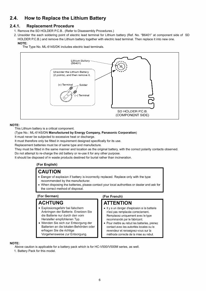
2.4. How to Replace the Lithium Battery2.4.1. Replacement Procedure
1. Remove the SD HOLDER P.C.B.. (Refer to Disassembly Procedures.)2. Unsolder the each soldering point of electric lead terminal for Lithium battery (Ref. No. “B6401” at component side of SD
HOLDER P.C.B.) and remove the Lithium battery together with electric lead terminal. Then replace it into new one.NOTE:
The Type No. ML-614S/DK includes electric lead terminals.
NOTE:This Lithium battery is a critical component. (Type No.: ML-614S/DN Manufactured by Energy Company, Panasonic Corporation)It must never be subjected to excessive heat or discharge.It must therefore only be fitted in requirement designed specifically for its use.Replacement batteries must be of same type and manufacture.They must be fitted in the same manner and location as the original battery, with the correct polarity contacts observed.Do not attempt to re-charge the old battery or re-use it for any other purpose.It should be disposed of in waste products destined for burial rather than incineration.
NOTE:Above caution is applicable for a battery pack which is for HC-V500/V500M series, as well.1. Battery Pack for this model.
6

3 Service Navigation3.1. IntroductionThis service manual contains technical information, which allow service personnel’s to understand and service this model.Please place orders using the parts list and not the drawing reference numbers.If the circuit is changed or modified, the information will be followed by service manual to be controlled with original service manual.
3.2. General Description About Lead Free Solder (PbF)The lead free solder has been used in the mounting process of all electrical components on the printed circuit boards used for thisequipment in considering the globally environmental conservation.The normal solder is the alloy of tin (Sn) and lead (Pb). On the other hand, the lead free solder is the alloy mainly consists of tin(Sn), silver (Ag) and Copper (Cu), and the melting point of the lead free solder is higher approx.30°C (86°F) more than that of thenormal solder.Distinction of P.C.B. Lead Free Solder being used
Service caution for repair work using Lead Free Solder (PbF)• The lead free solder has to be used when repairing the equipment for which the lead free solder is used.
(Definition: The letter of “PbF” is printed on the P.C.B. using the lead free solder.)• To put lead free solder, it should be well molten and mixed with the original lead free solder.• Remove the remaining lead free solder on the P.C.B. cleanly for soldering of the new IC.• Since the melting point of the lead free solder is higher than that of the normal lead solder, it takes the longer time to melt the
lead free solder.• Use the soldering iron (more than 70W) equipped with the temperature control after setting the temperature at 350±30°C
(662±86°F).Recommended Lead Free Solder (Service Parts Route.)
• The following 3 types of lead free solder are available through the service parts route.RFKZ03D01KS-----------(0.3mm 100g Reel)RFKZ06D01KS-----------(0.6mm 100g Reel)RFKZ10D01KS-----------(1.0mm 100g Reel)
Note* Ingredient: tin (Sn) 96.5%, silver (Ag) 3.0%, Copper (Cu) 0.5%, Cobalt (Co) / Germanium (Ge) 0.1 to 0.3%
3.3. Important Notice 1:(Other than U.S.A. and Canadian Market)1. The service manual does not contain the following information, because of the impossibility of servicing at component level
without concerned equipment/facilities.a. Schematic diagram, Block Diagram and P.C.B. layout of MAIN P.C.B..b. Parts list for individual parts for MAIN P.C.B..
When a part replacement is required for repairing MAIN P.C.B., replace as an assembled parts. (Main P.C.B.)2. The following category is /are recycle module part. Please send it/them to Central Repair Center.
• MAIN P.C.B. (VEP03J47A: HC-V500MP/PC/PU/EB/EC/EE/EG/EP/GA/GC/GK/GN/GT)• MAIN P.C.B. (VEP03J47C: HC-V500P/PC/EB/EC/EE/EF/EG/EP/GA/GC/GK/GN/GT)
7
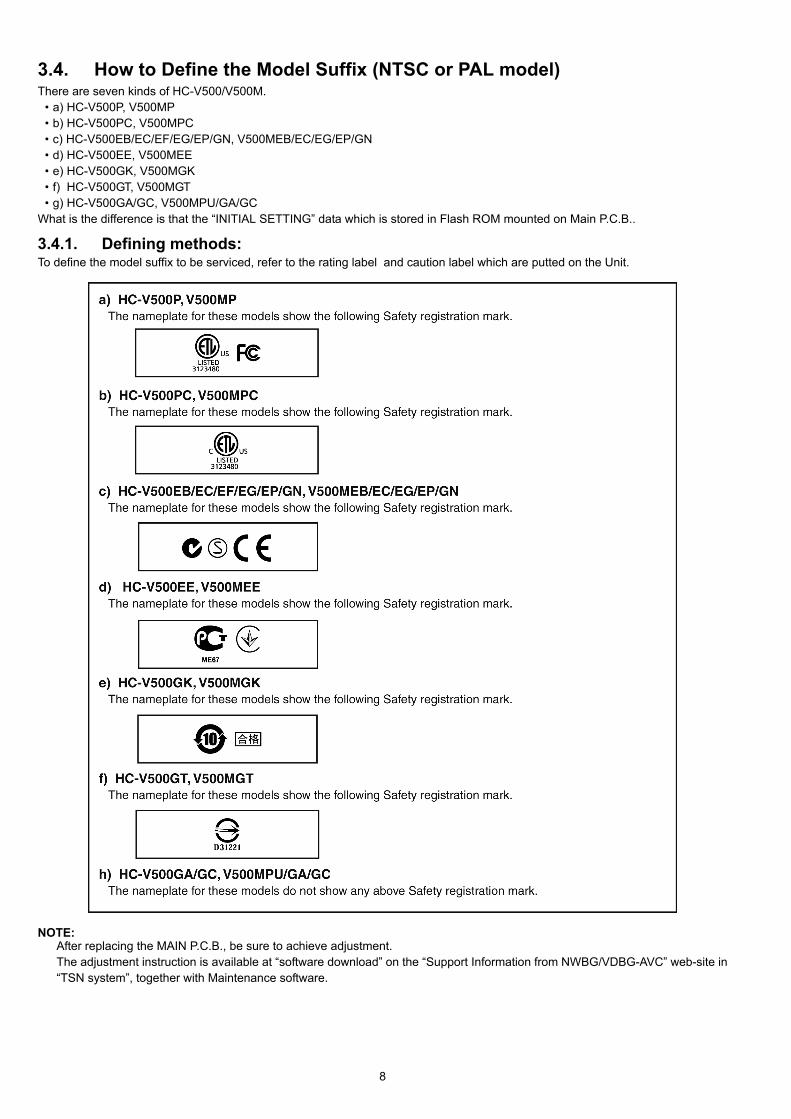
3.4. How to Define the Model Suffix (NTSC or PAL model)There are seven kinds of HC-V500/V500M.
• a) HC-V500P, V500MP• b) HC-V500PC, V500MPC• c) HC-V500EB/EC/EF/EG/EP/GN, V500MEB/EC/EG/EP/GN• d) HC-V500EE, V500MEE• e) HC-V500GK, V500MGK• f) HC-V500GT, V500MGT• g) HC-V500GA/GC, V500MPU/GA/GC
What is the difference is that the “INITIAL SETTING” data which is stored in Flash ROM mounted on Main P.C.B..
3.4.1. Defining methods:To define the model suffix to be serviced, refer to the rating label and caution label which are putted on the Unit.
NOTE:After replacing the MAIN P.C.B., be sure to achieve adjustment.The adjustment instruction is available at “software download” on the “Support Information from NWBG/VDBG-AVC” web-site in“TSN system”, together with Maintenance software.
8
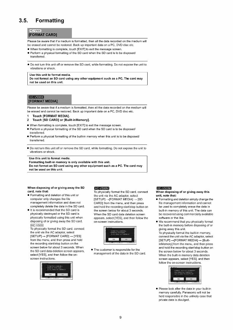
3.5. Formatting
9
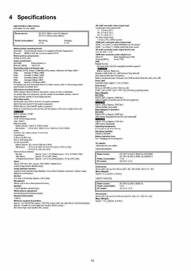
4 Specifications
10
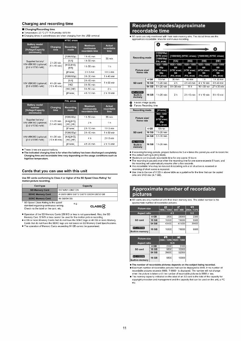
11

5 Location of Controls and Components1 Power button [ ]
2 Speaker
3 USB terminal [ ]
4 Intelligent auto/Manual button
[iA/MANUAL]
5 Optical image stabilizer button
[ O.I.S.]
6 1080/60p button [1080/60p] (NTSC areas)
7 Battery release lever [BATT]
8 HDMI mini connector [HDMI]
9 AV multi connector [AV MULTI]
● Use the AV multi cable (only the supplied
cable).
10 Lens cover
● The lens cover opens in Motion
Picture Recording Mode or Still
Picture Recording Mode.
11 LED light
● It can be used as a Video light or Photo
light.
12 Lens
13 Internal stereo microphones
2
456
3
7
1
AV MULTI
98
10
12
11
13
1080/50p button [1080/50p] (PAL areas)
14 Mode switch
15 Status indicator
16 Recording start/stop button
17 LCD monitor (Touch screen)
● It can open up to 90 .
● It can rotate up to 180 towards the lens
or 90 towards the opposite direction.
18 Battery holder
14 15 16
1817
Due to limitations in LCD production
technology, there may be some tiny bright
or dark spots on the LCD monitor screen.
However, this is not a malfunction and
does not affect the recorded picture.
12
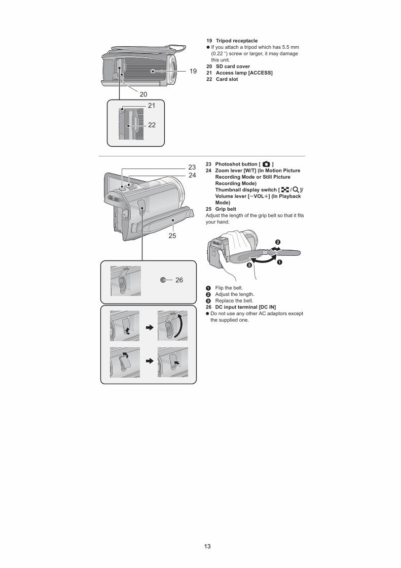
19 Tripod receptacle
● If you attach a tripod which has 5.5 mm
(0.22 ) screw or larger, it may damage
this unit.
20 SD card cover
21 Access lamp [ACCESS]
22 Card slot
19
21
22
20
23 Photoshot button [ ]
24 Zoom lever [W/T] (In Motion Picture
Recording Mode or Still Picture
Recording Mode)
Thumbnail display switch [ / ]/
Volume lever [ VOL ] (In Playback
Mode)
25 Grip belt
Adjust the length of the grip belt so that it fits
your hand.
Flip the belt.
Adjust the length.
Replace the belt.
26 DC input terminal [DC IN]
● Do not use any other AC adaptors except
the supplied one.
24
23
25
26
13

Change the mode to recording or playback.
Operate the mode switch to change the mode to , or .
You can operate by directly touching the LCD monitor (touch screen) with your finger.
■ Touch
Touch and release the touch screen to select icon or
picture.
● Touch the center of the icon.
● Touching the touch screen will not operate while
you are touching another part of the touch screen.
■ Slide while touching
Move your finger while pressing on the touch screen.
Selecting a mode
Motion Picture Recording Mode
Still Picture Recording Mode
Playback Mode
How to use the touch screen
■ About the operation icons
/ / / :
These icons are used to switch the menu and thumbnail
display page, for item selection and setting etc.
:
Touch to return to the previous screen such as when
setting menus.
14
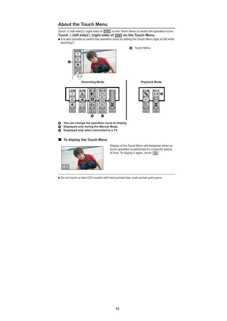
About the Touch Menu
Touch (left side)/ (right side) of on the Touch Menu to switch the operation icons.
Touch (left side)/ (right side) of on the Touch Menu.● It is also possible to switch the operation icons by sliding the Touch Menu right or left while
touching it.
You can change the operation icons to display.
Displayed only during the Manual Mode.
Displayed only when connected to a TV.
Touch Menu
Recording Mode Playback Mode
T
W
MENU
T
W
FOCUS
WB
SHTR
IRIS MENU
ALL
■ To display the Touch Menu
● Do not touch on the LCD monitor with hard pointed tips, such as ball point pens.
Display of the Touch Menu will disappear when no
touch operation is performed for a specific period
of time. To display it again, touch .
15

6 Service Mode1. Indication method of the service menu
Set the mode switch “Motion Picture Recording” mode.2. While the power is turned OFF, keep pressing the “Power” button, “Zoom lever” to W side and “intelligent auto/Manual” button
for more than 3 seconds until the top screen of the Service Mode Menu being displayed.
Service mode menu
NOTE:Do not using service mode except above table of Service mode menu.
3. End method of the top screen of the service mode menuTouch the [ EXIT ] of LCD to end the service mode, and then POWER OFF.
Screen display Contents Function1 Factory settings Function to throw a product up in a factory shipment state
(When recorded data in Built-in memory, “error display” is done)3 Built-in memory self check execution
(HC-V500M only)Function to check self as for the state of Built-in memory
4 Lock search history indication Display the camera system error cord for three histories savedin EEPROM
5 Power ON self check result display Power ON self check (function to diagnose correct function ofthe device and interface between devices) result display
10 Erasing the lock histories Erasing the error histories (working time is not erased)12 Camera data indications while the
video playbackDisplay the camera informations (Shutter speed, Iris value,White balance and focal length) while playing recorded video
16
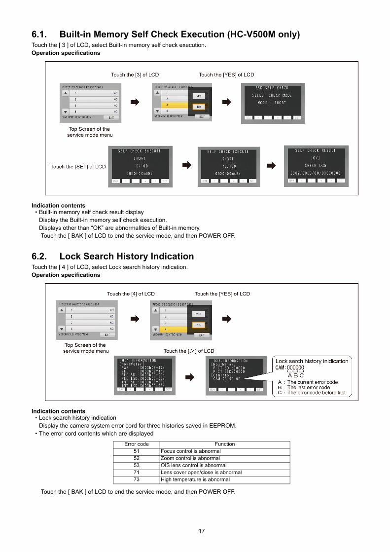
6.1. Built-in Memory Self Check Execution (HC-V500M only)Touch the [ 3 ] of LCD, select Built-in memory self check execution.Operation specifications
Indication contents• Built-in memory self check result display
Display the Built-in memory self check execution.Displays other than “OK” are abnormalities of Built-in memory.Touch the [ BAK ] of LCD to end the service mode, and then POWER OFF.
6.2. Lock Search History IndicationTouch the [ 4 ] of LCD, select Lock search history indication.Operation specifications
Indication contents• Lock search history indication
Display the camera system error cord for three histories saved in EEPROM.• The error cord contents which are displayed
Touch the [ BAK ] of LCD to end the service mode, and then POWER OFF.
Error code Function51 Focus control is abnormal52 Zoom control is abnormal53 OIS lens control is abnormal71 Lens cover open/close is abnormal73 High temperature is abnormal
17

6.3. Power ON Self Check Result DisplayTouch the [ 5 ] of LCD, select Power ON self check result display.Operation specifications
Indication contents• Power ON self check result display
Function to diagnose correct function of the device and interface between devices result display.
Display the following communication test result.- CAM-PWR : communication test between IC3401 and IC1503- CAM-UNI : Internal communication test of IC3401
Display other than “OK” are abnomalities of each lines.
Cutting of battery connection or AC power supply connection to end the service mode.
6.4. Erasing the lock historiesTouch the [ 10 ] of LCD, select erasing the lock histories execution.Operation specifications
Indication contents• Erasing the error histories stored in EEPROM. (working time is not erased)
Cutting of battery connection or AC power supply connection to end the service mode.
18
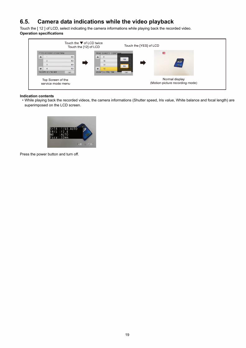
6.5. Camera data indications while the video playbackTouch the [ 12 ] of LCD, select indicating the camera informations while playing back the recorded video.Operation specifications
Indication contents• While playing back the recorded videos, the camera informations (Shutter speed, Iris value, White balance and focal length) are
superimposed on the LCD screen.
Press the power button and turn off.
19
7 Service Fixture & Tools7.1. When Replacing the Main P.C.B.After replacing the MAIN P.C.B., be sure to achieve adjustment.The adjustment instruction is available at “software download” on the “Support Information from NWBG/VDBG-AVC” web-site in“TSN system”, together with Maintenance software.
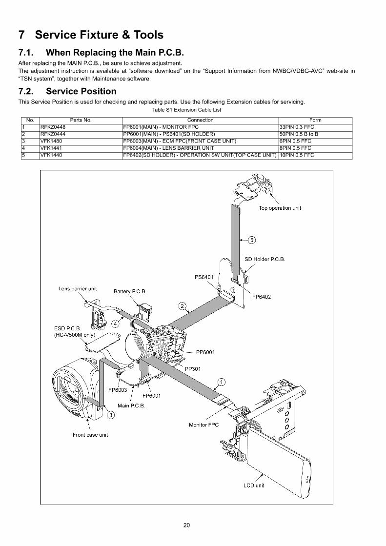
7.2. Service PositionThis Service Position is used for checking and replacing parts. Use the following Extension cables for servicing.
Table S1 Extension Cable List
No. Parts No. Connection Form1 RFKZ0448 FP6001(MAIN) - MONITOR FPC 33PIN 0.3 FFC2 RFKZ0444 PP6001(MAIN) - PS6401(SD HOLDER) 50PIN 0.5 B to B3 VFK1480 FP6003(MAIN) - ECM FPC(FRONT CASE UNIT) 6PIN 0.5 FFC4 VFK1441 FP6004(MAIN) - LENS BARRIER UNIT 8PIN 0.5 FFC5 VFK1440 FP6402(SD HOLDER) - OPERATION SW UNIT(TOP CASE UNIT) 10PIN 0.5 FFC
20

8 Disassembly and Assembly Instructions8.1. Disassembly Flow Chart for the UnitThis is a disassembling chart.When assembling, perform this chart conversely.
8.2. PCB Location
21
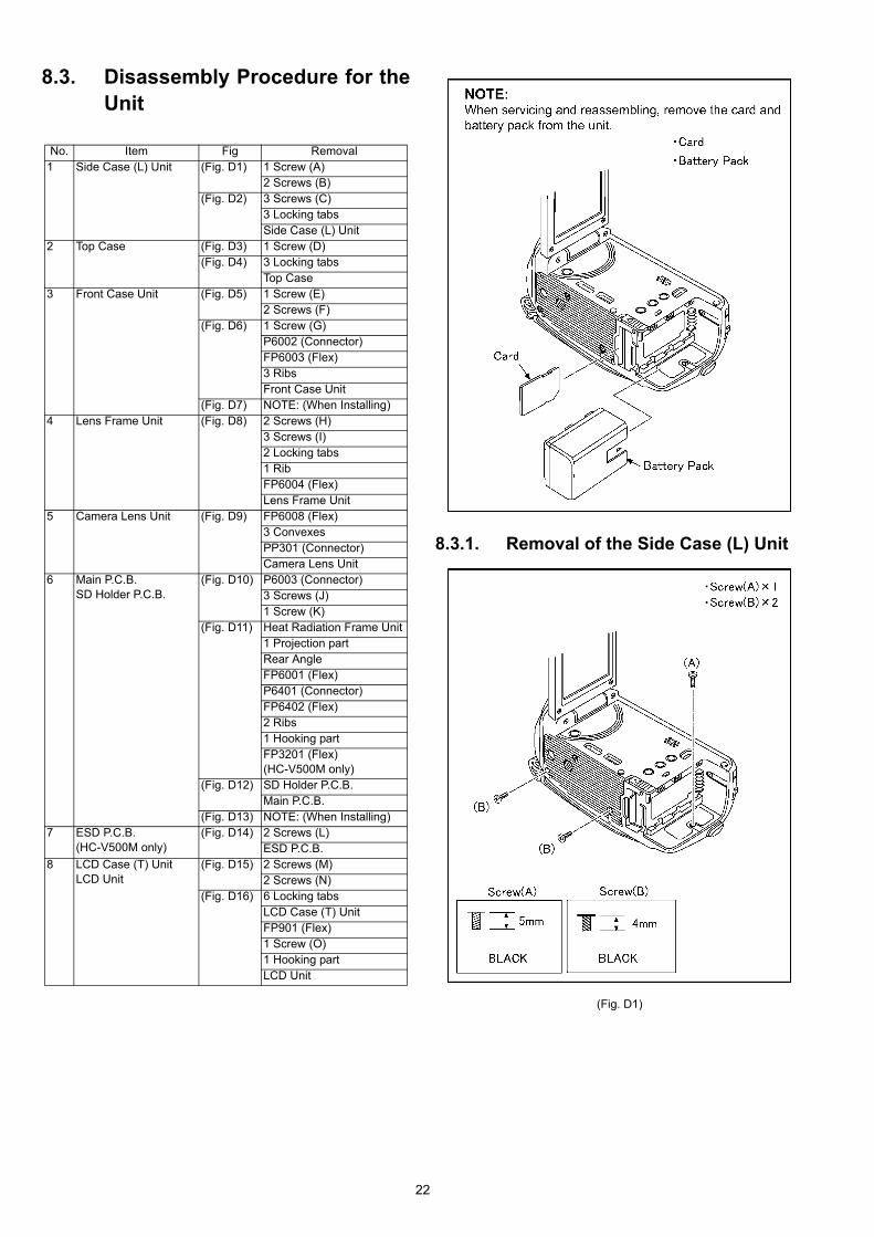
8.3. Disassembly Procedure for theUnit
8.3.1. Removal of the Side Case (L) Unit
(Fig. D1)
No. Item Fig Removal1 Side Case (L) Unit (Fig. D1) 1 Screw (A)
2 Screws (B)(Fig. D2) 3 Screws (C)
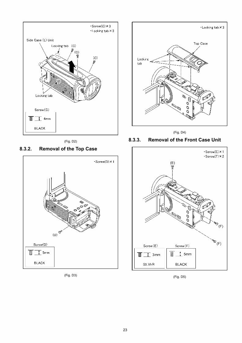
3 Locking tabsSide Case (L) Unit
2 Top Case (Fig. D3) 1 Screw (D)(Fig. D4) 3 Locking tabs
Top Case3 Front Case Unit (Fig. D5) 1 Screw (E)
2 Screws (F)(Fig. D6) 1 Screw (G)
P6002 (Connector)FP6003 (Flex)3 RibsFront Case Unit
(Fig. D7) NOTE: (When Installing)4 Lens Frame Unit (Fig. D8) 2 Screws (H)
3 Screws (I)2 Locking tabs1 RibFP6004 (Flex)Lens Frame Unit
5 Camera Lens Unit (Fig. D9) FP6008 (Flex)3 ConvexesPP301 (Connector)Camera Lens Unit
6 Main P.C.B. SD Holder P.C.B.
(Fig. D10) P6003 (Connector)3 Screws (J)1 Screw (K)
(Fig. D11) Heat Radiation Frame Unit1 Projection partRear AngleFP6001 (Flex)P6401 (Connector)FP6402 (Flex)2 Ribs1 Hooking partFP3201 (Flex) (HC-V500M only)
(Fig. D12) SD Holder P.C.B.Main P.C.B.
(Fig. D13) NOTE: (When Installing)7 ESD P.C.B.
(HC-V500M only)(Fig. D14) 2 Screws (L)
ESD P.C.B.8 LCD Case (T) Unit
LCD Unit(Fig. D15) 2 Screws (M)
2 Screws (N)(Fig. D16) 6 Locking tabs
LCD Case (T) UnitFP901 (Flex)1 Screw (O)1 Hooking partLCD Unit
22
(Fig. D2)
8.3.2. Removal of the Top Case
(Fig. D3)
(Fig. D4)
8.3.3. Removal of the Front Case Unit
(Fig. D5)
23

(Fig. D6)
(Fig. D7)
24
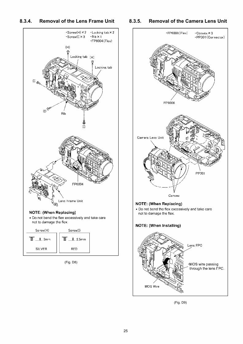
8.3.4. Removal of the Lens Frame Unit
(Fig. D8)
8.3.5. Removal of the Camera Lens Unit
(Fig. D9)
25

8.3.6. Removal of the Main P.C.B. and SDHolder P.C.B.
(Fig. D10)
(Fig. D11)
26

(Fig. D12)
(Fig. D13)
8.3.7. Removal of the ESD P.C.B.(HC-V500M only)
(Fig. D14)
27
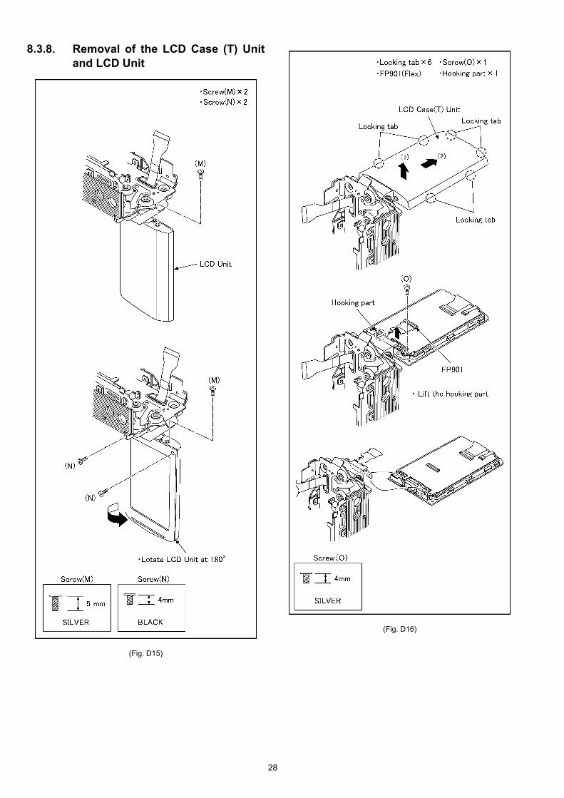
8.3.8. Removal of the LCD Case (T) Unitand LCD Unit
(Fig. D15)
(Fig. D16)
28
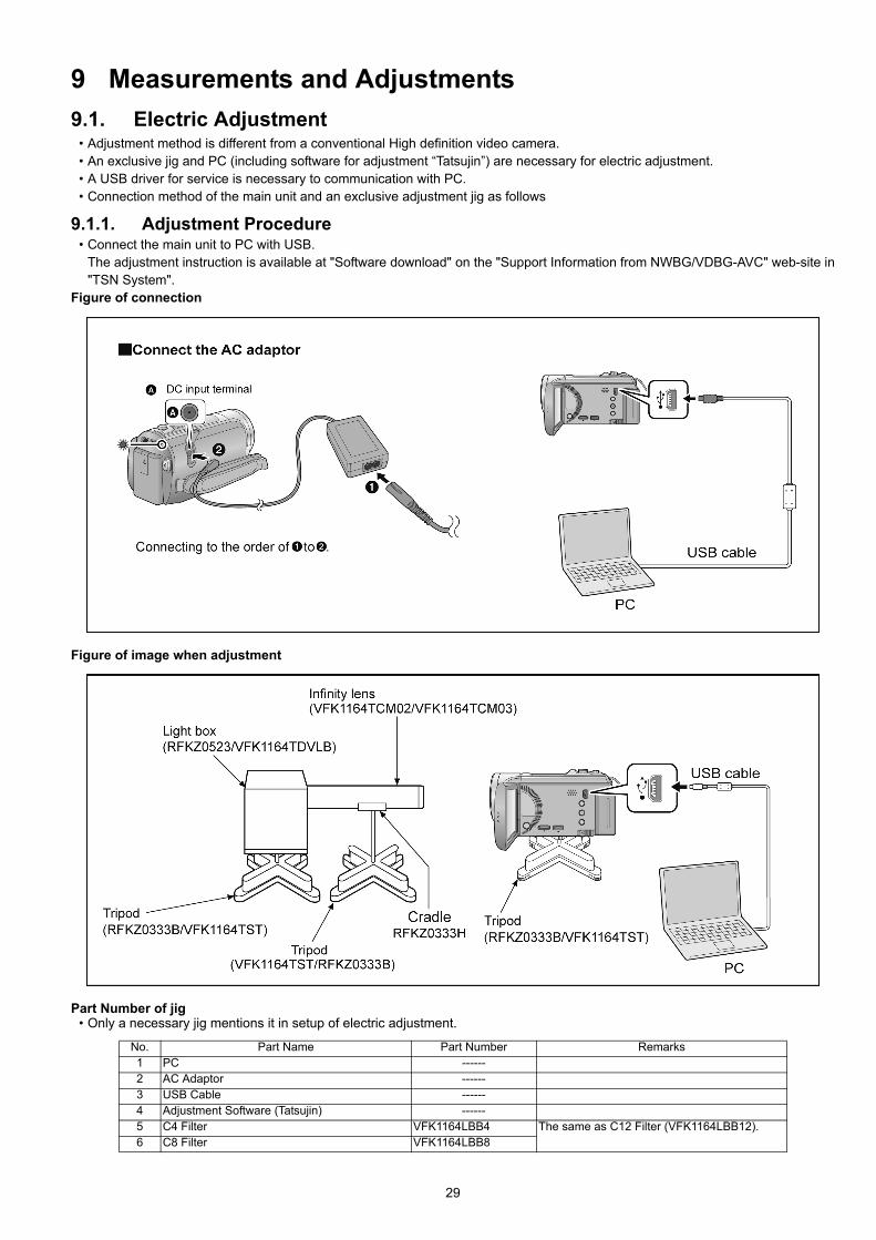
9 Measurements and Adjustments9.1. Electric Adjustment
• Adjustment method is different from a conventional High definition video camera.• An exclusive jig and PC (including software for adjustment “Tatsujin”) are necessary for electric adjustment.• A USB driver for service is necessary to communication with PC.• Connection method of the main unit and an exclusive adjustment jig as follows
9.1.1. Adjustment Procedure• Connect the main unit to PC with USB.
The adjustment instruction is available at "Software download" on the "Support Information from NWBG/VDBG-AVC" web-site in"TSN System".
Figure of connection
Figure of image when adjustment
Part Number of jig• Only a necessary jig mentions it in setup of electric adjustment.
No. Part Name Part Number Remarks1 PC ------2 AC Adaptor ------3 USB Cable ------4 Adjustment Software (Tatsujin) ------5 C4 Filter VFK1164LBB4 The same as C12 Filter (VFK1164LBB12).6 C8 Filter VFK1164LBB8
29

Adjustment Items• Adjustment item as follows.
The adjustment instruction is available at "Software download" on the "Support Information from NWBG/VDBG-AVC" web-site in"TSN System".
30
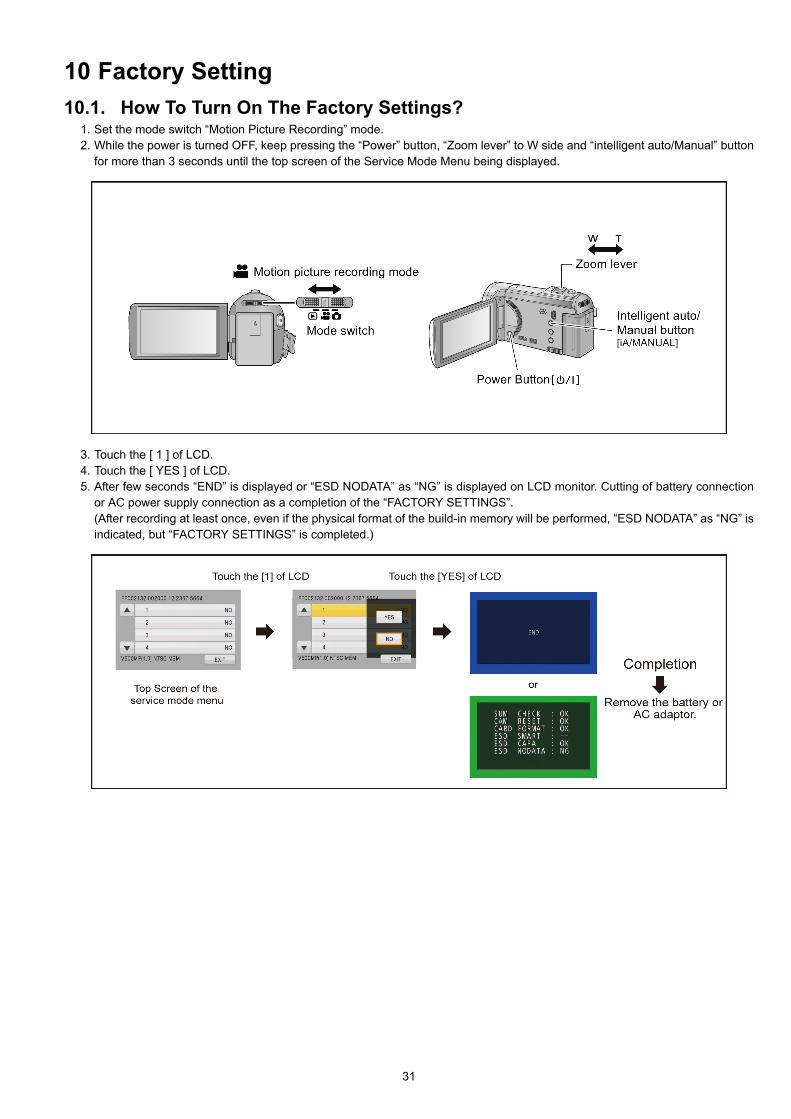
10 Factory Setting10.1. How To Turn On The Factory Settings?
1. Set the mode switch “Motion Picture Recording” mode.2. While the power is turned OFF, keep pressing the “Power” button, “Zoom lever” to W side and “intelligent auto/Manual” button
for more than 3 seconds until the top screen of the Service Mode Menu being displayed.
3. Touch the [ 1 ] of LCD.4. Touch the [ YES ] of LCD.5. After few seconds “END” is displayed or “ESD NODATA” as “NG” is displayed on LCD monitor. Cutting of battery connection
or AC power supply connection as a completion of the “FACTORY SETTINGS”.(After recording at least once, even if the physical format of the build-in memory will be performed, “ESD NODATA” as “NG” isindicated, but “FACTORY SETTINGS” is completed.)
31

10.2. What Is The Factory Settings?The factory settings clean up and/or refresh the following settings.
1. MENU, MODE, ADJUSTMENT VALUE.2. SD card format.3. Reset the folder number and file number of still pictures.
(Setting the folder number is 100, and file number is 0.)4. Clear the mechanism lock information.5. Clear the service mode information contents.6. Close the lens cover7. Initialize the VIERA Link Physical Address.
(HC-V500M)If the "Factory Settings" is completed, physical format of the build-in memory is not performed, execute physical format according tothe following procedure.
The setting position of factory settings:
Name Setting positionMode switch Motion picture recording mode
32

SD
CARD
SPEAKER
ECM
A/V
MULTI
TERMINAL
HDMI mini
CONNECTOR
Analog
Analog
Analog
Analog
AnalogIC3401
MPEG CODEC
(SPICa)
NOTE : VIDEO SIGNAL
: AUDIO SIGNAL
: CLK or CONTROL LINE
COLOR LCD
PANEL
IC3701
AVIO
IC3702
HD VIDEO
AMP
IC3201
INTERNAL MEMORY
/16GB
HC-V500M/V500 OVERALL BLOCK DIAGRAM
HC-V500M ONLY
IC3402
DDR SDRAM/
512Mbit
IC4801
MIC AMP
IC3403
NAND
FLASH ROM/
512Mbit
IC3405
RESET
10 Block Diagram10.1. Overall Block Diagram
OVERALL BLOCK DIAGRAM
IRIS
LENS(F1.8 4.2 38x)
IC701
LENS/OIS DRIVE
OPERATION
TOUCH PANEL
DC IN
BATTERY
SH
UT
TE
R IC201
MOS IMAGE
SENSOR
ZOOM/
FOCUS
MOTOR/
OIS
IC7101
PHOTO
LIGHT DRV
IC1001
POWER
IC1502
BATTERY
MONITOR
PHOTO LIGHT
X3402
OSC
(60MHz)
IC202,302
GATE ICIC705
LENS SHUTTER
DRIVE
X2303
(32.768kHz)
IC1503
RTC/CHARAGE/
POWER CONTROL
USB TERMINAL
IC301,703,704,1011,
1301,1421,1431,1471
REGULATOR
IC6401
GYRO
SENSOR
(PIT/YAW)
IC751
GYRO
SENSOR
(ROLL)
IC761
ROLL GYRO
AMP
IC2301
RESET
IC1501
VOLTAGE
DET.
IC511
MAGNETIC
SENSOR
33
X2303(32.768kHz)
S6001
LCD OPEN/CLOSE
CARD LED B
KEYIN4
POWER LED B
D6401
CARD
LED
PW REG3V
QR6402
FP905
X RIGHT
Y BOT
X LEFT
Y TOP
1
2
3
4
PW REG3V
PW REG3V
PW REG3V
V31
N29
P29
P30
P31
C28
B28
A29
B29
QR6006
PW REG3V
STANDBYLED B U30 QR6401
R30
QR3413 QR3411
QR3412
QR3410
A27
TOUCH PANEL
UNIT
QR6007
KEYIN1 A28
W29
IC1503(RTC/CHARGE/POWER CONTROL)
S6002
POWER ON/OFF
D3
G5
G6
/SWIN1
E3/SWIN2
XIN
XOUT
A5 LED
IC511(MAGNETIC SENSOR)
4
3
1
2VDD
OUT
GND
NC
HC-V500M/V500 CAMERA/SYSTEM CONTROL CIRCUIT BLOCK DIAGRAM
AD TPY RIGHT
AD TPY LEFT
AD TPX TOP
SEL2 ON LOW
SEL2 ON HI
LCD RVS
SEL1 ON HI
SEL1 ON LOW
AD TPX BOT
DI CHA
DO CHA
CLK CHA
CS CHA
L31
L30
L29
K31
B6 CS
B7 SCK
C6 SDI
C7 SDO
CH3422
CH3423
CH3424
QR3403
PW RTCVREG32
ZSW
(To IC701-49)
TOP OPERATION UNIT
FP6402
ZOOMAD
PHOTO1 HANOSHI
PHOTO2 ZENOSHI
2
3
4
5
7
8POWER LED
9
STANDBY LED
AVREF
AVREF
10VTR KEY 1
PW REG3V
S6404
S/S SW
S6403
IA
S6401
60P(NTSC)
50P(PAL)S6402
OISMODE SWITCH
ZOOM LEVER
PHOTO SHOT BUTTON
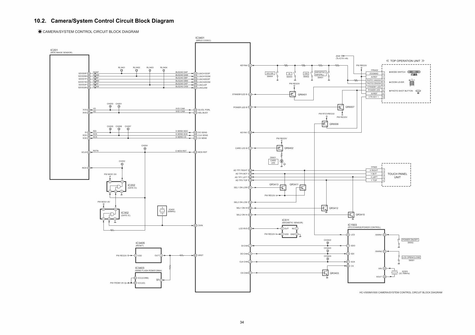
10.2. Camera/System Control Circuit Block Diagram
IC3401(MPEG CODEC)
CAMERA/SYSTEM CONTROL CIRCUIT BLOCK DIAGRAM
IC201(MOS IMAGE SENSOR)
AJ30 LVACH1DOP
LVACH1DOM
LVACH2DOP
LVACH2DOM
LVACLKP
LVACLKM
AJ31
AH28
X3402(60MHz)
5
1
4
32
IC302(GATE IC)
CH202
CH205 CH206
CH203 CH201
CH207
PW MOS1.8V
55
62
53SDOD0P
SDOD0M
SDOD1P
AH29
AH30
AH3163
54
64SDOD1M
SDOD2P
SDOD2M
RL3401 RL3402 RL3403 RL3404
IC3405(RESET)
XRST4VDDPW REG3V 2 AB31
CKINAE1
GLVDL PORLAF25
IC3403(NAND FLASH ROM/512Mbit)
RP 1754
55
VCC(CORE)
VCC(IO)PW FROM1.8V
OUT
BUS240 DAP
BUS240 DAM
BUS240 DBP
BUS240 DBM
BUS240 CKP
BUS240 CKM
49XVSXVD CAM
HDL BUSYAF2442XHSXHD CAM
DO SENSAH2235SIS SENS SDO
CLK SENSAF2136SCKS SENS SCK
CS SENSAH2114XCES SENS CS
MOS RSTAE2022XCLRE MOS RST
DOAP
DOAM
DOBP
DOBM
DCKP
DCKM
VD
HD
SDI
SCK
SCS
RSTN
50INCK
5
1
4
32
IC202(GATE IC)
PW MOS1.8V
CH204
34
AMCK
AIDAT
AD
M0
AD
M15
EC
LK
NF
CY
C
XE
CS
0 X
NF
CE
XE
WE
XN
FW
E
XE
RE
XN
FR
E
XA
VD
NFA
LE
NA
ND
RY
BY
FRO
M IN
T XN
FWP
C4 G8 C1 D2A3 C2 D1 E4D3
AODAT
E AVIO RST
MAIN CPU
HDMI
CONTROL
HDMI DMA I/F
CAMERA SIGNAL PROCESSOR
AUDIO DSP
DATA
M/512M-bit)
AL10
AK11
AJ11
AJ10
AL11
1019 36 53 56 147 8 21 28 35
CTL SIG
CS AVIO
HC-V500M/V500 VIDEO/AUDIO SIGNAL PROCESS(1) CIRCUIT BLOCK DIAGRAM
CLK+
CLK-
PW 3.2V
PR G PRA14
ALRCK AE11
ABCK1 AF11
PB G PBSDCA12
Y G HDYSDYA13
HD STBY HD STBYE29
29 33 47 49
DATA2+
DATA2-
DATA1+
DATA1-
DATA0+
DATA0-
HPD
SCL
SDA
CEC
1 8
72
FL6001
2
3
3 6
54
5
6
1 8
72
FL6002
8
9
14
3 6
54
11
12
15
16
19
PW 3.2V
JK6003
HDMI CONNECTOR
AK18TX2P
AK14
AJ13
CEC
HPD
AK13SDA
AL13SCL
AL18TX2M
AK17TX1P
AL17TX1M
AK16TX0P
AL16TX0M
AK15TXCP
AL15
AH1
AH6
AE6
AF6
AG2
AH2
AH3
AJ1
AJ2
TXCM
1
2
3
6
5
4
QR3402
Q3401
QR3401
To IC3701
(AUDIO AD/DA&VIDEO AMP)
To IC3702
(HD VIDEO AMP)
YCO LCD0
YCO LCD7
VCLKO LCD
YCO LCD1
YCO LCD2
YCO LCD3
YCO LCD4
YCO LCD5
YCO LCD6
H LCD AE8
V LCD AF8
DO LCDAVIO AL9
CLK LCDAVIO AK9
CS LCD AK10
LCD
CH907
CH906 CH903
CH901 CH902
CH905
BUS9 LCDYC0
BUS9 LCDYC1
BUS9 LCDYC2
BUS9 LCDYC3
BUS9 LCDYC4
BUS9 LCDYC5
BUS9 LCDYC6
BUS9 LCDYC7
BUS9 LCDH
BUS9 LCDV
S CS LCD
S DO LCD
S DO AVIO
S CLK LCD
S CLK AVIO
S CS AVIO
AIDAT0
AODAT0
E AVIO RST
CLK 12M
CLK LR1
CLK B1
CLK18 LCD
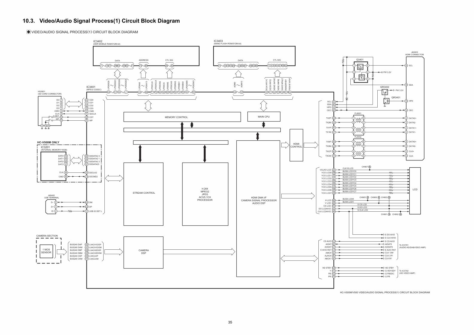
10.3. Video/Audio Signal Process(1) Circuit Block Diagram
1 MOS
SENSOR
CAMERA SECTION
IC3401(MPEG CODEC)
IC3201(INTERNAL MEMORY/16GB)
VIDEO/AUDIO SIGNAL PROCESS(1) CIRCUIT BLOCK DIAGRAM
3
4
2
USB TERMINAL
D-
D+
JK6402
AC4 G1 U3 M4
LP
D0C
LK
LP
D0X
CLK
LP
D0C
KE
LP
D0C
S
LP
D0W
E
LP
D0C
AS
LP
D0R
AS
P2 N4P1 M3 N3 R4
LP
D0B
A1
LP
D0B
A0
T4 R3N2
MEMORY CONTROL
CAMERA
DSP
H.264
MPEG2
JPEG
AC3/5.1CH
PROCESSOR
IC3403(NAND FLASH RO
18
AL24
AL25
Y31
DM
DP
USB ID DET LID
STREAM CONTROL
AJ30 LVACH1DOP
LVACH1DOM
LVACH2DOP
LVACH2DOM
LVACLKP
LVACLKM
AJ31
AH28
AH29
AH30
AH31
BUS240 DAP
BUS240 DAM
BUS240 DBP
BUS240 DBM
BUS240 CKP
BUS240 CKM
IC3402(DDR MOBILE RAM/512M-bit)
28 40 11 13
LP
D0D
Q0
LP
D0D
Q31
W3 M2
LP
D0D
M0
LP
D0D
M3
W4 L1
LP
D0D
QS
0
LP
D0D
QS
3
LP
D0A
0
LP
D0A
13
ADDRESS CTL SIG
17 267 14 52 59 62 71 73 85
DATA
HC-V500M ONLY
7
8
9
1
2
5
10
12
D0
D1
D2
D3
CMD
CLKC.DET
WP
11
U3
V1
U2
V3
T2
T1
U5
U1
HS3901
(SD CARD CONNECTOR)
CD0
CD1
CD2
CD3
CMD
SDCLK
CDT
WP
13 14
DAT0
DAT1
DAT2
DAT3
G20
F20
F21
G21
C20
C19
CLK
CMD
SDCLK2
SDCMD2
H3
H4
H5
J2
W6
W5
SDDATA2 0
SDDATA2 1
SDDATA2 2
SDDATA23
35
HC-V500M/V500 VIDEO/AUDIO SIGNAL PROCESS(2) CIRCUIT BLOCK DIAGRAM
JK6002
(AV JACK)
VOUT1
PLUGIN L9
HDYOUT2
PBOUT6
PROUT10
LOUT5
ROUT11
SPEAKER
PW 5V
IC3702(HD VIDEO AMP)
9
10
13 1
2
8
7
6dB
6dB
6dB
5
4
14 15
3
Y IN
PB IN
PR IN
CP GND C MINUS
Y OUT
PB OUT
PR OUT
VEE OUT
VEE IN
12
PW 3.2V
IC3701(AVIO)
37
I2S IF
MCLK
39BCLK
38LRCLK
LPF
14YIN BUF
CLAMPPGA
15CIN BUF
CLAMPPGA
+ 18VOUT
SERIAL IF/
REGISTER
3CS X
4SCLK
5SDIN
36RESET X
1DAC DIN
2ADC DOUT
31LIN L
PGAADC
16bit
32LIN R
PGAADC
16bit
ALC
CONT.INTERFACE
DAC
16bit
DAC
16bit
SEL
SEL
MIXAMP
CONTROL
25SPP
22SPN
29LOUTL
30LOUTR
19VDDV5
26VDDH
12VDDV
35VDDANA
12VDDV
35VDDANA
8VDDIO
6VDDDIG
23VDDSP
PW REG3V
PW SPK3.2V
PLUG IN L
(To IC3401-E30)
STBY
CHARGE PUMP
27MHz LPF
15MHz LPF
15MHz LPF
NVCC
C PLUS
CPVCC
STBY
RL3706
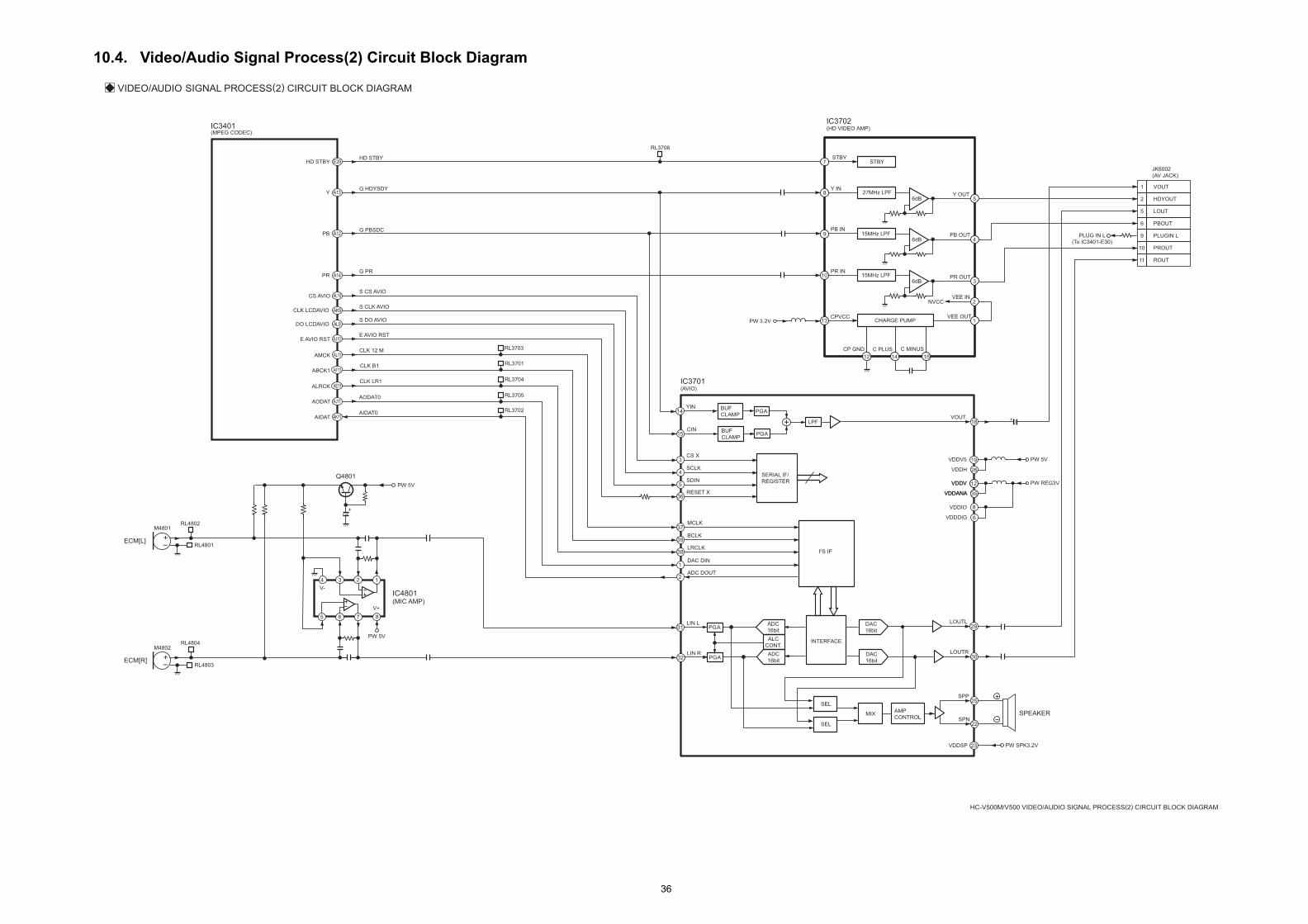
10.4. Video/Audio Signal Process(2) Circuit Block Diagram
VIDEO/AUDIO SIGNAL PROCESS(2) CIRCUIT BLOCK DIAGRAM
+-
+-
ECM[R]
ECM[L]
M4802
M4801RL4802
RL4801
RL4804
RL4803
RL3703
RL3701
RL3704
RL3705
RL3702
IC4801(MIC AMP)
4
5
2
7 8
1
6
3
Q4801
V-
V+
PW 5V
PW 5V
+
CLK 12 M
E AVIO RST
S DO AVIO
S CLK AVIO
S CS AVIO
G PR
G PBSDC
G HDYSDY
HD STBY
CLK B1
CLK LR1
IC3401(MPEG CODEC)
AIDAT0
AODAT0
AMCK
AIDAT
AODAT
E AVIO RST
AL10
AK11
AJ11
AJ10
AL11
CS AVIO
PR A14
ALRCK AE11
ABCK1 AF11
PB A12
Y A13
HD STBY E29
DO LCDAVIO AL9
CLK LCDAVIO AK9
36
IC3401(MPEG CODEC)
PW REG3V
QR751
LENS BALEA LED CNT
PW GYRO3V
HD225
NSCS LEN
SCK LEN
SDO LEN
VD60
PW STNOREG
AL28
AK27
J30
J31
K29
N30
U31
CH728
CH711
CH3426
CH3425
SDI LEN
DACLD LEN
E LENS RST
K30
J29
D30
S GSE PL SCL
S GSE PL SDA
LEDDRV FLASH
LEDDRV TORCH
(GYRO SENSOR: PIT/YAW)
11 MOSI
10 MISO
8 CSB
CL6401 CL6406
CL6402
CL6403
9 SCLK
CL64041VCC
7VDD
PW LENS3V
IC751
IC6401
(GYRO SENSOR: ROLL)
4 VOUT
1 VREF
3VCC
S GSE PL SCL
D25
C27
PHOTO TEMP2
PHOTO TEMP1
S GSE PL SDA
P ZABS LEN
FABS LEN
AA30
F31
ZABS LENF30
F29
P FABS LENE31
LENS TEMPA25
SHTR OPENR29
LEDCONT LEN
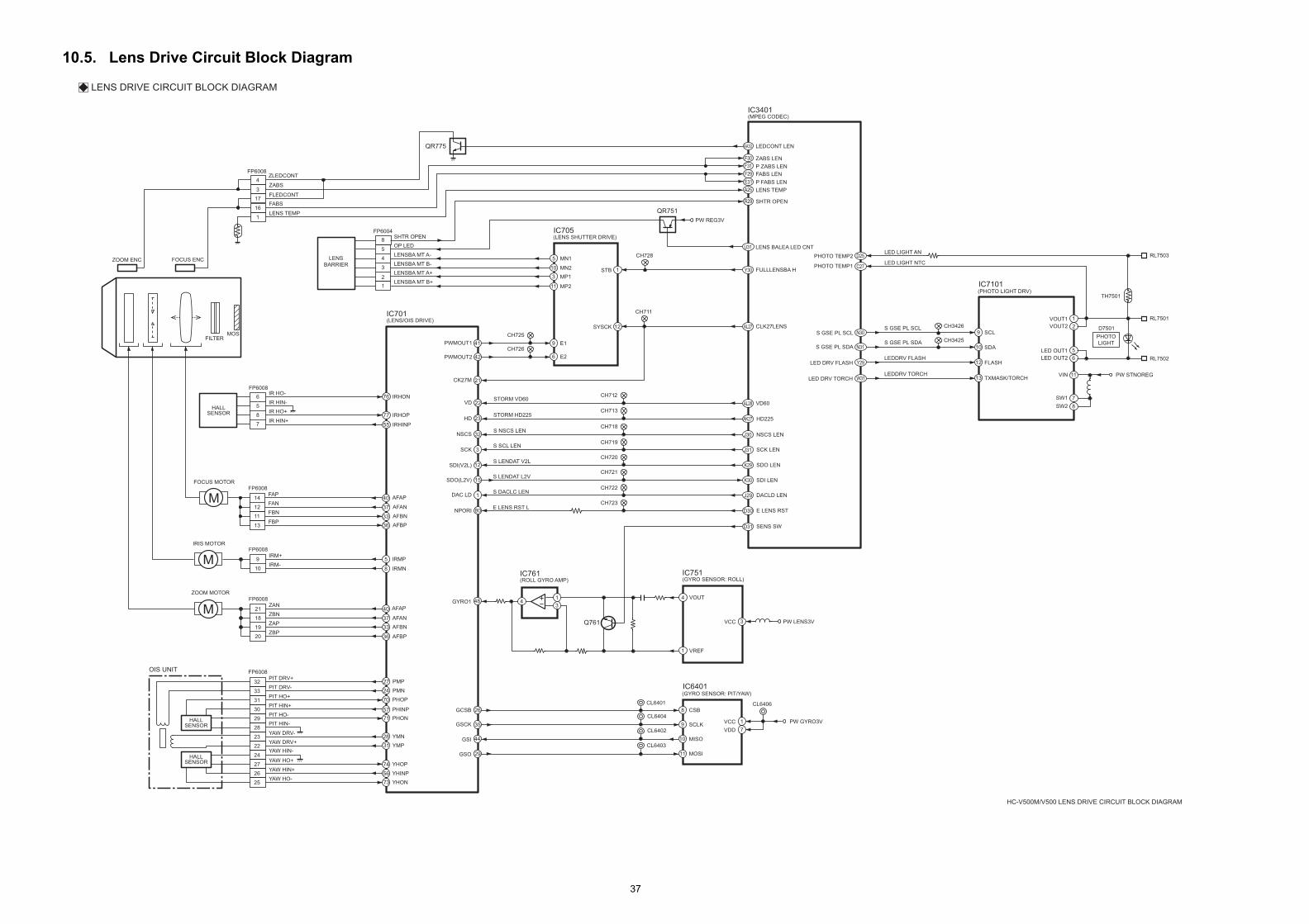
HC-V500M/V500 LENS DRIVE CIRCUIT BLOCK DIAGRAM
FULLLENSBA HY30
CLK27LENSAL27
IC7101(PHOTO LIGHT DRV)
9
1
2SCL
VOUT1
VOUT2
5
6
LED OUT1
LED OUT2
11VIN
8SW2
7SW1
10 SDA
12 FLASH
13 TXMASK/TORCH
N31
Y29LED DRV FLASH
W31LED DRV TORCH
RL7501
RL7503
TH7501
RL7502
D7501
PHOTO
LIGHT
SENS SWD31
LED LIGHT AN
LED LIGHT NTC
10.5. Lens Drive Circuit Block Diagram
FILTERMOS
M
5
8
7
21
18
19
20
IC701(LENS/OIS DRIVE)
6
ZAP
ZBP
M
IRIS MOTOR
FP6008
ZBN
ZAN
9
HALLSENSOR
HALLSENSOR
OIS UNIT FP6008PIT DRV+
PIT DRV-
PIT HO+
PIT HIN+
YAW DRV-
YAW DRV+
YAW HIN+
YAW HIN-
YAW HO-
32
33
31
30
29
28
23
22
24
27
26
25
PIT HO-
PIT HIN-
YAW HO+
IRM+
IRM-
FP6008
FP6008
IR HO+
IR HIN+
IR HO-
IR HIN-HALL
SENSOR
PMP
IRHOP
76 IRHON
31
71
YMP
PHON
28 YMN
70
24
PHOP
57 PHINP
PMN
77
27
IRHINP55
IRMP5
IRMN8
AFBN
40 AFAP
33
AFAN37
AFBP36
73 YHON
74
56
YHOP
YHINP
GCSB
GSCK
GSI
GSO
GYRO1
29
23
32
3
12
HD
NSCS
SCK
SDI(V2L)
SDO(L2V)
DAC LD
NPORI
22VD
10
CH712
CH725
CH726
CH713
CH718
CH719
CH720
15
1
80
CH721
CH722
CH723
42
PWMOUT1
PWMOUT2
FP6004
4
3
2
1
5
SHTR OPEN
OP LED
LENSBA MT A-
LENSBA MT B-
LENSBA MT A+
LENSBA MT B+
LENS
BARRIER
8
44
26
35
IC761(ROLL GYRO AMP)
481
3
ZOOM ENC
FP6008
4
17
3
16
1
FLEDCONT
FABS
LENS TEMP
ZABS
QR775
ZLEDCONT
ZOOM MOTOR
FOCUS ENC
4
41
(LENS SHUTTER DRIVE)
5 MN1
10 MN2
3 MP1
11 MP2
9 E1
6 E2
1STB
SYSCK
IC705
12
21CK27M
M
FOCUS MOTOR
FAP
FAN
FBN
FBP
14
12
11
13
FP6008
AFAN
40 AFAP
37
AFBN33
AFBP36
Q761
STORM VD60
STORM HD225
S NSCS LEN
S SCL LEN
S LENDAT V2L
S LENDAT L2V
S DACLC LEN
E LENS RST L
LENS DRIVE CIRCUIT BLOCK DIAGRAM
37

CL1461
DCG
LX7
RT
FLT7
INV6
VREF5
INV4
VCC
INV7
PGND4
STB6
HS
6L
HX
567
LE
D
VO2S
LX1
PGND13
LX3
VO2
LX22
HX13
SELDRV
SCP
LX21
PGND2
INV
1
ST
B5
HX
4
UD
SE
L
VO
7
VR
EG
A
HX
2
LX
4
PW
M7
ST
B1234
INV
3
LX
5
INV
5
GN
D
PG
ND
567
LX
6
22 21 1820 1719 16 15 14 13 12
23
24
25
26
27
28
29
30
31
32
33
11
10
9
8
7
6
5
4
3
2
1
37 38 39 40 4134 35 36
IC1001(POWER)
HC-V500M/V500 POWER SUPPLY CIRCUIT BLOCK DIAGRAM
PW SPK3.2V
PW LENS3.2V
PW 3.2V
PW REG3V
CL1331
CL1422
PW VBUS
PW 5V
PW HDM5V
PW RTCVREG32
CL1301
CL1011
CL1421
CL1321PW SD3.2V
1 3
QR1002
QR1001
QR1101
5
1
4
32
IC1301(REGULATOR)GND
VOUTVIN
NP
VBUS ON H
(From IC3401-U29)
CL1351
CL1371
CL1471
5
1
4
32
IC1471(REGULATOR)GND
VOUTVIN
NCCONT.
V OUT
NP
VIN
VCONT
5
1
4
32
IC1011(REGULATOR)GND
24
23
22
21
AN0
P07
VIN12
AT ON H
20
19
18
17
HG ON H
VIN2
BAT IN
P06
16
TX
D
25
AN
2
AN
1
IC1501(VOLTAGE DET.)
2
1
3
4OUT
VSS
VDD
NC
PW STNOREG
(To IC7101-11)
R1261
QR2308
CL1102
CL1105
CL1101
CL1103
1-AF7)
IC1431(REGULATOR)
3
2
4
1
VIN
VOUT
STBY
GND
PW PLL1.1V
PW LENS1.5V
PW VID1.1V
PW 5.4V
PW REG1.8V
PW FROM1.8V
PW SENS1.8V
CH1231
CH1101
CL1341
IC703(REGULATOR)
3
2
4
1
VIN
VOUT
STBY
GND
D902-905
(LCD BACK LIGHT)
CL1001
CL1002
6 45
2
IC1421(REGULATOR)NOISE
VIN VOUTVOUT
GNDSTBYIC704(REGULATOR)
3
2
4
1
VIN
VOUT
STBY
GND
PW LENS3V
5
1
4
32
IC301(REGULATOR)
GND
OUTIN
NCCE
MOSSENS ON H
(From IC3401-AF20)
PW MOS2.7V
VCONT
10.6. Power Supply Circuit Block Diagram
POWER SUPPLY CIRCUIT BLOCK DIAGRAM
JK6701
1
3
4
2
+
T
D
-
JK6401
1
3
2
+
-
BATTERY
DC IN FUSE RESISTOR:
Q1501
1 2 3 4
568 7
IC1502(BATTERY
MONITOR)
32
1
2
3
4
5
6
7
8
31 30 29
9 10 11 12
VSS
CS
AFE DI
AFE CLKIN
/RESET OUT
LED CONT
A0
VDD
B
RIN
ISE
NS
0
ISE
NS
1
VR
EG
VN
VS
S
AF
E D
O
P01
VS
S
C
13 14 15
AF
E C
LK
OU
T
BK
UP
CO
NT
RX
D
28 27 26
VC
C
AN
3
Q1502
1 2 3 4
568 7
1 2 3
46 5
Q1503
IC3401(MPEG CODEC)
DI CHA
DO CHA
CLK CHA
CS CHA
SW NOREG
FGMICOM RXD
FGMICOM TXD
FGMICOM SCK
CS FG
L31
L30
L29
K31
H31
H30
H29
G31
B25
T31
QR1503
R1001
IC2301(RESET)
1
2
4
3VDD
GND
CD
OUT
Q1504
PW REG3V
BL CONT
(From IC340
BATT RXD
AL29USB DET H
T30BATT TXD
G29FG RST H
IC1503(RTC/CHARGE/POWER CONTROL)
/SWIN3
VREG32
D6
E4
WKUP F3
B2USB
A1OUT
C2
A3
USBSW
BAT DEC
G2VREG25
(R1001/R1261/R6412)
Please check the Fuse Rsistor when an output
voltage does not output.
IP1502
IP6401
1
USB TERMINAL
VBUS
JK6402
ADPSW
PWSW
A2 ADP
C1 VADP
SW
F2
USB DETE6
E2
E7BAT
E1VUSB
D7 ISNS
F7 TDET
B6 CS
B7 SCK
E5SWIN4
F4WKUP RST
C6 SDI
C7 SDO
S6002
POWER ON/OFF
LI BATT
D3 /SWIN1
B6401
G4COINBAT
G3
DVIN A6
CHG EN F5
FULLSET D2
BATSET D1
USB EN F6
USB WK CNT B4
R6412
CH3422
CH3423
CH3424
QR3403
38
HC-V500M/V500 INTERCONNECTION DIAGRAM
MAIN P.C.B. (FOIL SIDE)
: (COMPONENT SIDE)
SD HOLDER P.C.B. (FOIL SIDE)
FP
6004
8 6 4 2
SH
TR
OP
EN
D G
ND
LE
NS
BA
MT
A-
LE
NS
BA
MT
A+
LENSBARRIER
P6003
6 5 4 3 2 1
BA
TT-
BA
TT-
D TB
AT
T+
BA
TT
+
D G
ND
OP
EN
LE
DL
EN
SB
A M
T B
-L
EN
SB
A M
T B
+
FB
PF
EN
CV
CC
FLE
DC
ON
TZ
AP
ZA
NY
AW
DR
V-
YA
WH
O-
YA
WH
O+
PIT
HO-
PIT
HO
+P
ITD
RV-
12
14
16
18
20
22
24
26
28
30
32
FA
NFA
PFA
BS
ZB
NZ
BP
YA
WD
RV
+Y
AW
HIN
-Y
AW
HIN
+P
ITH
IN-
PIT
HIN
+P
ITD
RV
+
13
15
17
19
21
23
25
27
29
31
33
PP301
12345678901234567890
NCNCNC
RSTNSDIHD
SCKSCSVD
MCLK2.7V
DOBPDOBMDCKPDCKMDOAPDOAM1.8V1.8V1.8V
PP6001
CARD LED BNOREGNOREGNOREGNOREGNOREGNOREGD GND
PW REG3VVBUSVBUSD GND
ZOOMADD GND
POWER LEDSTANDBY LED
VTR KEY 1E CARD DETPW SD3R2VPW SD3R2VPW SD3R2V
IDPW LIBATTE KEYIN4
E CARD PRO
SD CMDDGND
SD DATA2SD DATA3SD DATA0SD DATA1
DGNDSD CLKD GNDD GNDD GND
S GYRO CSBS GYRO SCKS GYRO SOS GYRO SI
PW GYRO3VG EPGYRO REFG EPGYRORGYRO GND
SP OUT2SP OUT1D GND
D+D-
D GND
25242322212019181716151413121110987654321
26272829303132333435363738394041424344454647484950
P6701
123456
BATT +BATT +
TD
BATT -BATT -
JK
67
01
1 2 3 4
+ T D -
BATTERY
BATTERY CATCHER P.C.B.(FOIL SIDE)
: (COMPONENT SIDE)
PS6401
CA
RD
LE
D B
NO
RE
GN
OR
EG
NO
RE
GN
OR
EG
NO
RE
GN
OR
EG
D G
ND
PW
RE
G3V
VB
US
VB
US
D G
ND
ZO
OM
AD
D G
ND
PO
WE
R L
ED
STA
ND
BY
LE
DV
TR
KE
Y 1
E C
AR
D D
ET
PW
SD
3R
2V
PW
SD
3R
2V
PW
SD
3R
2V
IDP
W L
IBA
TT
E K
EY
IN4
E C
AR
D P
RO
SD
CM
DD
GN
DS
D D
ATA
2S
D D
ATA
3S
D D
ATA
0S
D D
ATA
1D
GN
DS
D C
LK
D G
ND
D G
ND
D G
ND
S G
YR
O C
SB
S G
YR
O S
CK
S G
YR
O S
OS
GY
RO
SI
PW
GY
RO
3V
G E
PG
YR
O R
EF
G E
PG
YR
OR
GY
RO
GN
DS
P O
UT
2S
P O
UT
1D
GN
DD
+D-
D_G
ND
25
24
23
22
21
20
19
18
17
16
15
14
13
12
11
10 9 8 7 6 5 4 3 2 1
26
27
28
29
30
31
32
33
34
35
36
37
38
39
40
41
42
43
44
45
46
47
48
49
50
FP
64
02
10 9 8 7 6 5 4 3 2 1
VT
R K
EY
1A
VR
EF
PO
WE
R L
ED
STA
ND
BY
LE
DG
ND
PH
OT
O2
ZE
NO
SH
IP
HO
TO
1 H
AN
OS
HI
AV
RE
FZ
OO
M A
DG
ND
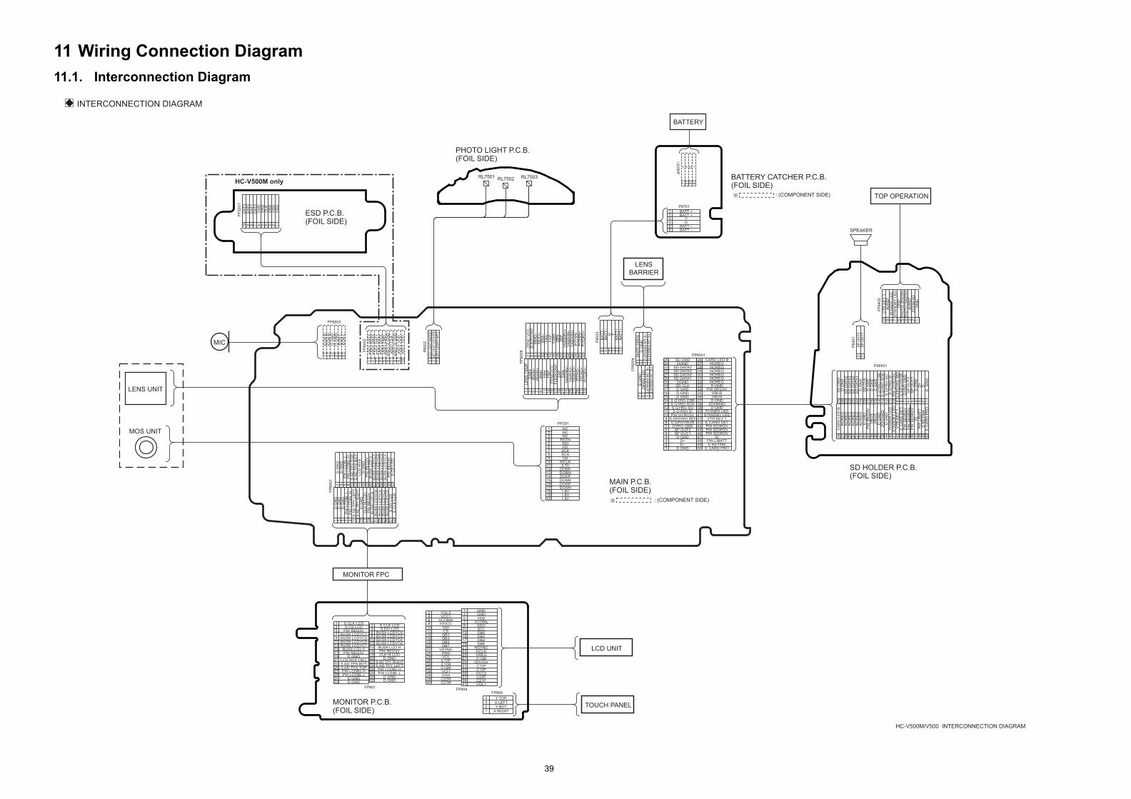
TOP OPERATION
SPEAKER
P6401
2 1S
P O
UT
2S
P O
UT
1
LCD UNIT
7 5 3 1
TOUCH PANEL
11 Wiring Connection Diagram11.1. Interconnection Diagram
INTERCONNECTION DIAGRAM
ESD P.C.B.(FOIL SIDE)
MONITOR P.C.B.(FOIL SIDE)
LE
NS
TE
MP
ZA
BS
IRH
IN-
IRH
IN+
IRM
+F
BN
2 4 6 8 10
ZE
NC
VC
CZ
LE
DC
ON
TIR
HO-
IRH
O+
IRM-
1 3 5 7 9 11
FP
6008P
6002
3 2 1
LE
D L
IGH
T A
NO
DE
LED
LIG
HT
CAT
HO
DE
LE
D L
IGH
T N
TC
11111111112
D G
ND
D G
ND
D G
ND
PW
LC
DB
L L
PW
LC
DB
L H
S A
D T
PY
LE
FT
S A
D T
PY
RIG
HT
D G
ND
CLK
18 L
CD
PW
RE
G3V
BU
S9 L
CD
HB
US
9 L
CD
YC
6B
US
9 L
CD
YC
4B
US
9 L
CD
YC
2B
US
9 L
CD
YC
0S
DO
LC
DS
CLK
LC
D
2 4 6 8 10
12
14
16
18
20
22
24
26
28
30
32
D G
ND
D G
ND
PW
LC
DB
L L
PW
LC
DB
L H
S A
D T
PX
TO
PS
AD
TP
X B
OT
LC
D R
VS
D G
ND
PW
RE
G3V
BU
S9 L
CD
VB
US
9 L
CD
YC
7B
US
9 L
CD
YC
5B
US
9 L
CD
YC
3B
US
9 L
CD
YC
1P
W R
EG
3V
S C
S L
CD
1 3 5 7 9 11
13
15
17
19
21
23
25
27
29
31
33
FP
6001
MONITOR FPC
FP
6002
1 2 3 4 5 6 7 8 9 10
eS
D1 D
AT
3eS
D1 D
AT
0eS
D1 D
AT
1eS
D1 D
AT
2eS
D1 C
MD
eS
D1 D
GN
DeS
D1 C
LK
eS
D1 D
GN
DeS
D1 V
DD
eS
D1 V
DD
FP60031 2 3 4 5 6
EC
M R
EC
M R
D G
ND
D G
ND
EC
M L
EC
M L
FP
32
01
10 9 8 7 6 5 4 3 2 1
DA
T3
DA
T0
DA
T1
DA
T2
CM
DG
ND
CLK
GN
DV
DD
VD
D
PHOTO LIGHT P.C.B.(FOIL SIDE)
RL7501 RL7503RL7502
S CLK LCDS CS LCD
PW REG3VBUS9 LCDYC1BUS9 LCDYC3BUS9 LCDYC5BUS9 LCDYC7BUS9 LCD VPW REG3V
D GNDLCD RVS ON LS AD TPX BOTS AD TPX TOPPW LCDBL HPW LCDBL L
D GNDD GND
2468
101214161820222426283032
S CLK LCDS DO LCD
BUS9 LCDYC0BUS9 LCDYC2BUS9 LCDYC4BUS9 LCDYC6BUS9 LCD HPW REG3VCLK18 LCD
D GNDS AD TPY RIGHTS AD TPY LEFTPW LCDBL HPW LCDBL L
D GNDD GND
13579111315171921232527293133
FP901FP904
GNDGNDVDD
VCOMLSDOSCLDB0DB2DB4DB6
HSYNCDCLKVREGC13M
DDVDHC11PC12PVCC2C22PC21PVGL1
2468
10121416182022242628303234363840
VGL2VCC1
VCOMHIOVCC
SDICS
DB1DB3DB5DB7
VSYNCGNDVCL
C13PC11MC12MVCI1VGHC22MC21M
1357911131517192123252729313335373941
MOS UNIT
LENS UNIT
MIC
HC-V500M only
Y TOPX LEFTY BOT
X RIGHT
4321
FP905
39
Model No. : HC-V500/V500M Schematic Diagram Note

Model No. : HC-V500/V500M Parts List Note

Model No. : HC-V500/V500M Main Connection (Main P.C.B.)

Model No. : HC-V500/V500M Video (Main P.C.B.)

Model No. : HC-V500/V500M Lens Drive (Main P.C.B.)
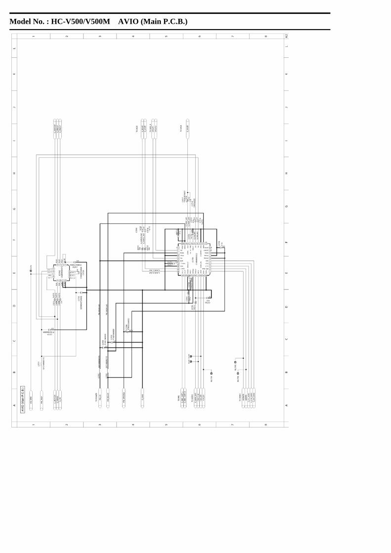
Model No. : HC-V500/V500M AVIO (Main P.C.B.)

Model No. : HC-V500/V500M HDMI (Main P.C.B.)
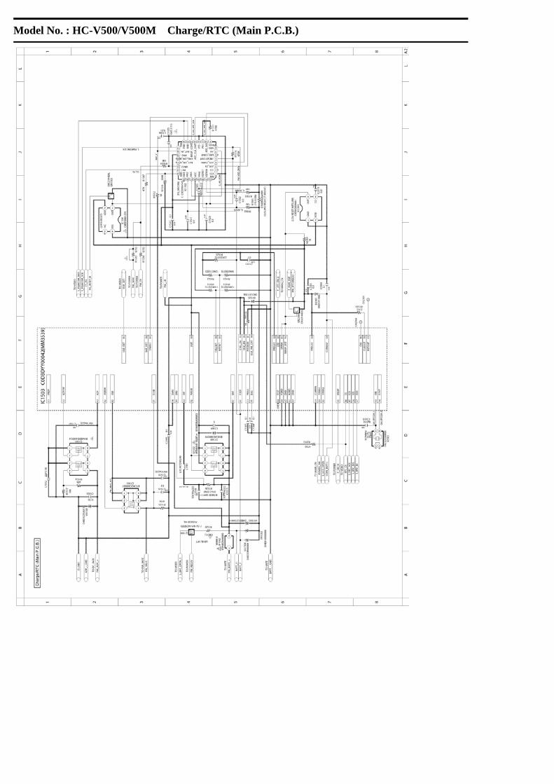
Model No. : HC-V500/V500M Charge/RTC (Main P.C.B.)

Model No. : HC-V500/V500M MIC (Main P.C.B.)

Model No. : HC-V500/V500M Photo Light (Main P.C.B.)
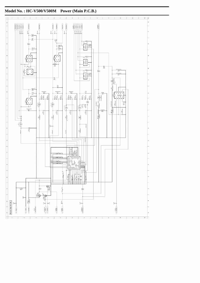
Model No. : HC-V500/V500M Power (Main P.C.B.)

Model No. : HC-V500/V500M MOS Connection (Main P.C.B.)
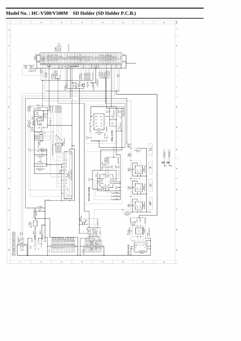
Model No. : HC-V500/V500M SD Holder (SD Holder P.C.B.)

Model No. : HC-V500/V500M Main P.C.B. (Component Side)

Model No. : HC-V500/V500M Main P.C.B. (Foil Side)

Model No. : HC-V500/V500M SD Holder P.C.B.(Component Side)

Model No. : HC-V500/V500M SD Holder P.C.B.(Foil Side)

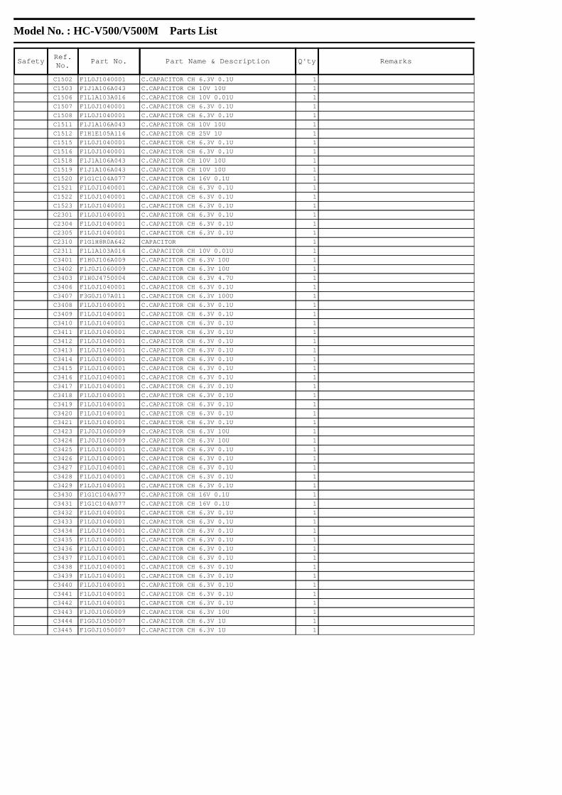
Model No. : HC-V500/V500M Parts List
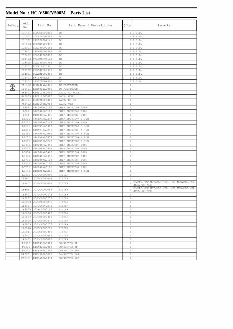
Safety Ref. No. Part No. Part Name & Description Q'ty Remarks
B6401 ML-614S/DK BATTERY 1
C302 F1L0J1040001 C.CAPACITOR CH 6.3V 0.1U 1
C303 F1G0J1050007 C.CAPACITOR CH 6.3V 1U 1
C304 F1G0J1050007 C.CAPACITOR CH 6.3V 1U 1
C305 F1G1C104A077 C.CAPACITOR CH 16V 0.1U 1
C309 F1G0J1050007 C.CAPACITOR CH 6.3V 1U 1
C701 F1G0J1050007 C.CAPACITOR CH 6.3V 1U 1
C702 F1G0J1050007 C.CAPACITOR CH 6.3V 1U 1
C703 F1J1A106A043 C.CAPACITOR CH 10V 10U 1
C704 F1G0J1050007 C.CAPACITOR CH 6.3V 1U 1
C705 F1G0J1050007 C.CAPACITOR CH 6.3V 1U 1
C706 F1G0J1050007 C.CAPACITOR CH 6.3V 1U 1
C708 F1J1A106A043 C.CAPACITOR CH 10V 10U 1
C709 F1J1A106A043 C.CAPACITOR CH 10V 10U 1
C715 F1G1C104A077 C.CAPACITOR CH 16V 0.1U 1
C716 F1L1A103A016 C.CAPACITOR CH 10V 0.01U 1
C718 F1G1E1030005 C.CAPACITOR CH 25V 0.01U 1
C719 F1G1E1030005 C.CAPACITOR CH 25V 0.01U 1
C720 F1G1E1030005 C.CAPACITOR CH 25V 0.01U 1
C721 F1G1E1030005 C.CAPACITOR CH 25V 0.01U 1
C722 F1G1E1030005 C.CAPACITOR CH 25V 0.01U 1
C723 F1G1E1030005 C.CAPACITOR CH 25V 0.01U 1
C724 F1G1E1030005 C.CAPACITOR CH 25V 0.01U 1
C725 F1G1E1030005 C.CAPACITOR CH 25V 0.01U 1
C726 F1G1E1030005 C.CAPACITOR CH 25V 0.01U 1
C727 F1G1E1030005 C.CAPACITOR CH 25V 0.01U 1
C751 F1J1A106A043 C.CAPACITOR CH 10V 10U 1
C753 F1L0J1040001 C.CAPACITOR CH 6.3V 0.1U 1
C761 F1G1E1030005 C.CAPACITOR CH 25V 0.01U 1
C763 F1J0J226A088 C.CAPACITOR CH 6.3V 22U 1
C765 F1G0J1050007 C.CAPACITOR CH 6.3V 1U 1
C767 F1G1C104A077 C.CAPACITOR CH 16V 0.1U 1
C771 F1L0J1040001 C.CAPACITOR CH 6.3V 0.1U 1
C772 F1L0J1040001 C.CAPACITOR CH 6.3V 0.1U 1
C777 F1G1C104A077 C.CAPACITOR CH 16V 0.1U 1
C1001 F1J1A106A043 C.CAPACITOR CH 10V 10U 1
C1012 F1G1H102A640 C.CAPACITOR CH 50V 1000P 1
C1013 F1G0J1050007 C.CAPACITOR CH 6.3V 1U 1
C1061 F1H0J4750004 C.CAPACITOR CH 6.3V 4.7U 1
C1101 F1G0J1050007 C.CAPACITOR CH 6.3V 1U 1
C1102 F1G1C104A077 C.CAPACITOR CH 16V 0.1U 1
C1103 F1G0J1050007 C.CAPACITOR CH 6.3V 1U 1
C1161 F1G0J1050007 C.CAPACITOR CH 6.3V 1U 1
C1221 F1G0J1050007 C.CAPACITOR CH 6.3V 1U 1
C1222 F1J1A106A043 C.CAPACITOR CH 10V 10U 1
C1231 F1G0J1050007 C.CAPACITOR CH 6.3V 1U 1
C1232 F1J1A106A043 C.CAPACITOR CH 10V 10U 1
C1242 F1J1A106A043 C.CAPACITOR CH 10V 10U 1
C1251 F1G0J1050007 C.CAPACITOR CH 6.3V 1U 1
C1252 F1J1A106A043 C.CAPACITOR CH 10V 10U 1
C1261 F1H1E105A116 C.CAPACITOR CH 25V 1U 1
C1271 F1G0J1050007 C.CAPACITOR CH 6.3V 1U 1
C1272 F1J1A106A043 C.CAPACITOR CH 10V 10U 1
C1273 F1G1H220A644 C.CAPACITOR CH 50V 22P 1
C1303 F1G1H102A640 C.CAPACITOR CH 50V 1000P 1
C1304 F1G0J1050007 C.CAPACITOR CH 6.3V 1U 1
C1342 F3F0G4760004 E.CAPACITOR CH 4V 47U 1
C1356 F3F0G4760004 E.CAPACITOR CH 4V 47U 1
C1422 F1G0J1050007 C.CAPACITOR CH 6.3V 1U 1
C1431 F1H0J4750004 C.CAPACITOR CH 6.3V 4.7U 1
C1471 F1G0J1050007 C.CAPACITOR CH 6.3V 1U 1
C1501 F1J1A106A043 C.CAPACITOR CH 10V 10U 1
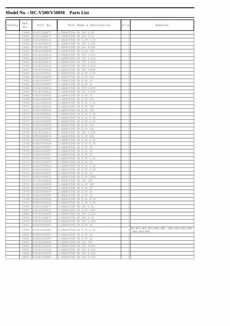
Model No. : HC-V500/V500M Parts List
Safety Ref. No. Part No. Part Name & Description Q'ty Remarks
C1502 F1L0J1040001 C.CAPACITOR CH 6.3V 0.1U 1
C1503 F1J1A106A043 C.CAPACITOR CH 10V 10U 1
C1506 F1L1A103A016 C.CAPACITOR CH 10V 0.01U 1
C1507 F1L0J1040001 C.CAPACITOR CH 6.3V 0.1U 1
C1508 F1L0J1040001 C.CAPACITOR CH 6.3V 0.1U 1
C1511 F1J1A106A043 C.CAPACITOR CH 10V 10U 1
C1512 F1H1E105A116 C.CAPACITOR CH 25V 1U 1
C1515 F1L0J1040001 C.CAPACITOR CH 6.3V 0.1U 1
C1516 F1L0J1040001 C.CAPACITOR CH 6.3V 0.1U 1
C1518 F1J1A106A043 C.CAPACITOR CH 10V 10U 1
C1519 F1J1A106A043 C.CAPACITOR CH 10V 10U 1
C1520 F1G1C104A077 C.CAPACITOR CH 16V 0.1U 1
C1521 F1L0J1040001 C.CAPACITOR CH 6.3V 0.1U 1
C1522 F1L0J1040001 C.CAPACITOR CH 6.3V 0.1U 1
C1523 F1L0J1040001 C.CAPACITOR CH 6.3V 0.1U 1
C2301 F1L0J1040001 C.CAPACITOR CH 6.3V 0.1U 1
C2304 F1L0J1040001 C.CAPACITOR CH 6.3V 0.1U 1
C2305 F1L0J1040001 C.CAPACITOR CH 6.3V 0.1U 1
C2310 F1G1H8R0A642 CAPACITOR 1
C2311 F1L1A103A016 C.CAPACITOR CH 10V 0.01U 1
C3401 F1H0J106A009 C.CAPACITOR CH 6.3V 10U 1
C3402 F1J0J1060009 C.CAPACITOR CH 6.3V 10U 1
C3403 F1H0J4750004 C.CAPACITOR CH 6.3V 4.7U 1
C3406 F1L0J1040001 C.CAPACITOR CH 6.3V 0.1U 1
C3407 F3G0J107A011 C.CAPACITOR CH 6.3V 100U 1
C3408 F1L0J1040001 C.CAPACITOR CH 6.3V 0.1U 1
C3409 F1L0J1040001 C.CAPACITOR CH 6.3V 0.1U 1
C3410 F1L0J1040001 C.CAPACITOR CH 6.3V 0.1U 1
C3411 F1L0J1040001 C.CAPACITOR CH 6.3V 0.1U 1
C3412 F1L0J1040001 C.CAPACITOR CH 6.3V 0.1U 1
C3413 F1L0J1040001 C.CAPACITOR CH 6.3V 0.1U 1
C3414 F1L0J1040001 C.CAPACITOR CH 6.3V 0.1U 1
C3415 F1L0J1040001 C.CAPACITOR CH 6.3V 0.1U 1
C3416 F1L0J1040001 C.CAPACITOR CH 6.3V 0.1U 1
C3417 F1L0J1040001 C.CAPACITOR CH 6.3V 0.1U 1
C3418 F1L0J1040001 C.CAPACITOR CH 6.3V 0.1U 1
C3419 F1L0J1040001 C.CAPACITOR CH 6.3V 0.1U 1
C3420 F1L0J1040001 C.CAPACITOR CH 6.3V 0.1U 1
C3421 F1L0J1040001 C.CAPACITOR CH 6.3V 0.1U 1
C3423 F1J0J1060009 C.CAPACITOR CH 6.3V 10U 1
C3424 F1J0J1060009 C.CAPACITOR CH 6.3V 10U 1
C3425 F1L0J1040001 C.CAPACITOR CH 6.3V 0.1U 1
C3426 F1L0J1040001 C.CAPACITOR CH 6.3V 0.1U 1
C3427 F1L0J1040001 C.CAPACITOR CH 6.3V 0.1U 1
C3428 F1L0J1040001 C.CAPACITOR CH 6.3V 0.1U 1
C3429 F1L0J1040001 C.CAPACITOR CH 6.3V 0.1U 1
C3430 F1G1C104A077 C.CAPACITOR CH 16V 0.1U 1
C3431 F1G1C104A077 C.CAPACITOR CH 16V 0.1U 1
C3432 F1L0J1040001 C.CAPACITOR CH 6.3V 0.1U 1
C3433 F1L0J1040001 C.CAPACITOR CH 6.3V 0.1U 1
C3434 F1L0J1040001 C.CAPACITOR CH 6.3V 0.1U 1
C3435 F1L0J1040001 C.CAPACITOR CH 6.3V 0.1U 1
C3436 F1L0J1040001 C.CAPACITOR CH 6.3V 0.1U 1
C3437 F1L0J1040001 C.CAPACITOR CH 6.3V 0.1U 1
C3438 F1L0J1040001 C.CAPACITOR CH 6.3V 0.1U 1
C3439 F1L0J1040001 C.CAPACITOR CH 6.3V 0.1U 1
C3440 F1L0J1040001 C.CAPACITOR CH 6.3V 0.1U 1
C3441 F1L0J1040001 C.CAPACITOR CH 6.3V 0.1U 1
C3442 F1L0J1040001 C.CAPACITOR CH 6.3V 0.1U 1
C3443 F1J0J1060009 C.CAPACITOR CH 6.3V 10U 1
C3444 F1G0J1050007 C.CAPACITOR CH 6.3V 1U 1
C3445 F1G0J1050007 C.CAPACITOR CH 6.3V 1U 1
Model No. : HC-V500/V500M Parts List
Safety Ref. No. Part No. Part Name & Description Q'ty Remarks
C3446 F1G1C104A077 C.CAPACITOR CH 16V 0.1U 1
C3447 F1G1C104A077 C.CAPACITOR CH 16V 0.1U 1
C3449 F1L0J1040001 C.CAPACITOR CH 6.3V 0.1U 1
C3450 F1L1A103A016 C.CAPACITOR CH 10V 0.01U 1
C3451 F1G1H472A571 C.CAPACITOR CH 50V 4700P 1
C3452 F1H0J106A009 C.CAPACITOR CH 6.3V 10U 1
C3453 F1L1A103A016 C.CAPACITOR CH 10V 0.01U 1
C3454 F1L1A103A016 C.CAPACITOR CH 10V 0.01U 1
C3455 F1L1A103A016 C.CAPACITOR CH 10V 0.01U 1
C3456 F1L1A103A016 C.CAPACITOR CH 10V 0.01U 1
C3457 F1G1H102A640 C.CAPACITOR CH 50V 1000P 1
C3459 F1L0J1040001 C.CAPACITOR CH 6.3V 0.1U 1
C3460 F1H0J106A009 C.CAPACITOR CH 6.3V 10U 1
C3461 F1G0J1050007 C.CAPACITOR CH 6.3V 1U 1
C3462 F1G0J1050007 C.CAPACITOR CH 6.3V 1U 1
C3464 F1L1A103A016 C.CAPACITOR CH 10V 0.01U 1
C3465 F1L1A103A016 C.CAPACITOR CH 10V 0.01U 1
C3466 F1G0J1050007 C.CAPACITOR CH 6.3V 1U 1
C3468 F1H0J106A009 C.CAPACITOR CH 6.3V 10U 1
C3469 F1L0J1040001 C.CAPACITOR CH 6.3V 0.1U 1
C3470 F1J0J1060009 C.CAPACITOR CH 6.3V 10U 1
C3471 F1J0J1060009 C.CAPACITOR CH 6.3V 10U 1
C3472 F1L0J1040001 C.CAPACITOR CH 6.3V 0.1U 1
C3473 F1L0J1040001 C.CAPACITOR CH 6.3V 0.1U 1
C3474 F1L0J1040001 C.CAPACITOR CH 6.3V 0.1U 1
C3701 F1J0J1060009 C.CAPACITOR CH 6.3V 10U 1
C3702 F1J0J1060009 C.CAPACITOR CH 6.3V 10U 1
C3703 F1L1A103A016 C.CAPACITOR CH 10V 0.01U 1
C3704 F3F0J226A016 T.CAPACITOR CH 6.3V 22U 1
C3705 F1L0J1040001 C.CAPACITOR CH 6.3V 0.1U 1
C3706 F1H0J4750004 C.CAPACITOR CH 6.3V 4.7U 1
C3707 F1G0J1050007 C.CAPACITOR CH 6.3V 1U 1
C3709 F1G0J1050007 C.CAPACITOR CH 6.3V 1U 1
C3710 F1G0J1050007 C.CAPACITOR CH 6.3V 1U 1
C3712 F1L0J1040001 C.CAPACITOR CH 6.3V 0.1U 1
C3713 F1G0J1050007 C.CAPACITOR CH 6.3V 1U 1
C3714 F1L0J1040001 C.CAPACITOR CH 6.3V 0.1U 1
C3715 F1L0J1040001 C.CAPACITOR CH 6.3V 0.1U 1
C3716 F1G0J1050007 C.CAPACITOR CH 6.3V 1U 1
C3717 F3G0J107A011 C.CAPACITOR CH 6.3V 100U 1
C3718 F1J1A106A043 C.CAPACITOR CH 10V 10U 1
C3731 F1J0J1060009 C.CAPACITOR CH 6.3V 10U 1
C3732 F1G0J1050007 C.CAPACITOR CH 6.3V 1U 1
C3733 F1G0J1050007 C.CAPACITOR CH 6.3V 1U 1
C3734 F1G0J1050007 C.CAPACITOR CH 6.3V 1U 1
C3736 F1H0J4750004 C.CAPACITOR CH 6.3V 4.7U 1
C3737 F1H0J4750004 C.CAPACITOR CH 6.3V 4.7U 1
C3906 F1G1C104A077 C.CAPACITOR CH 16V 0.1U 1
C3907 F3G0J107A011 C.CAPACITOR CH 6.3V 100U 1
C3908 F1G1E1030005 C.CAPACITOR CH 25V 0.01U 1
C3909 F1G1C104A077 C.CAPACITOR CH 16V 0.1U 1
C3910 F1G1E1030005 C.CAPACITOR CH 25V 0.01U 1
C3911 F1G0J1050007 C.CAPACITOR CH 6.3V 1U 1
C3956 F1L0J1040001 C.CAPACITOR CH 6.3V 0.1U 1 MP,MPC,MPU,MGT,MEG,MEC, MEP,MEB,MGC,MGA ,MEE,MGN,MGK
C4801 F1G0J1050007 C.CAPACITOR CH 6.3V 1U 1
C4802 F1G0J1050007 C.CAPACITOR CH 6.3V 1U 1
C4803 F1J1A106A043 C.CAPACITOR CH 10V 10U 1
C4804 F1G1H332A640 C.CAPACITOR CH 50V 3300P 1
C4805 F1G1E1030005 C.CAPACITOR CH 25V 0.01U 1
C4806 F1G1E1030005 C.CAPACITOR CH 25V 0.01U 1
C4807 F1G1E1030005 C.CAPACITOR CH 25V 0.01U 1

Model No. : HC-V500/V500M Parts List
Safety Ref. No. Part No. Part Name & Description Q'ty Remarks
C4809 F1G1H332A640 C.CAPACITOR CH 50V 3300P 1
C4810 F1G1E1030005 C.CAPACITOR CH 25V 0.01U 1
C4812 F1J1A106A043 C.CAPACITOR CH 10V 10U 1
C6003 F1L0J1040001 C.CAPACITOR CH 6.3V 0.1U 1
C6004 F1G1C104A077 C.CAPACITOR CH 16V 0.1U 1
C6005 F1G1H472A571 C.CAPACITOR CH 50V 4700P 1
C6006 F1G1H472A571 C.CAPACITOR CH 50V 4700P 1
C6008 F1G1H680A644 C.CAPACITOR CH 50V 68P 1
C6009 F1G1H680A644 C.CAPACITOR CH 50V 68P 1
C6010 F1G1H680A644 C.CAPACITOR CH 50V 68P 1
C6011 F1G1H680A644 C.CAPACITOR CH 50V 68P 1
C6012 F1G1H680A644 C.CAPACITOR CH 50V 68P 1
C6013 F1G1H680A644 C.CAPACITOR CH 50V 68P 1
C6014 F1G1H680A644 C.CAPACITOR CH 50V 68P 1
C6015 F1G1H680A644 C.CAPACITOR CH 50V 68P 1
C6018 F1L0J1040001 C.CAPACITOR CH 6.3V 0.1U 1
C6022 F1L0J1040001 C.CAPACITOR CH 6.3V 0.1U 1
C6023 F1L0J1040001 C.CAPACITOR CH 6.3V 0.1U 1
C6030 F1L0J1040001 C.CAPACITOR CH 6.3V 0.1U 1
C6403 F1G1C104A077 C.CAPACITOR CH 16V 0.1U 1
C6404 F1G1C104A077 C.CAPACITOR CH 16V 0.1U 1
C6405 F1G1C104A077 C.CAPACITOR CH 16V 0.1U 1
C6407 F1G1C104A077 C.CAPACITOR CH 16V 0.1U 1
C6408 ECJ1VB1A105K C.CAPACITOR CH 10V 1U 1
C6412 F1H1E105A116 C.CAPACITOR CH 25V 1U 1
C6421 F1J0J1060009 C.CAPACITOR CH 6.3V 10U 1
C7101 F1J1A106A043 C.CAPACITOR CH 10V 10U 1
C7103 F1J1A106A043 C.CAPACITOR CH 10V 10U 1
D1261 B0JCMD000077 DIODE 1 E.S.D.
D1271 B0JCGD000016 DIODE 1 E.S.D.
D1503 B0JCMC000019 DIODE 1 E.S.D.
D1505 DB2S31100L DIODE 1 E.S.D.
D2301 DB2S31100L DIODE 1 E.S.D.
D3401 DB2S31100L DIODE 1 E.S.D.
D3402 DB2S31100L DIODE 1 E.S.D.
D3403 DB2S31100L DIODE 1 E.S.D.
D6401 B3AAB0000343 LED 1 E.S.D.
FL3401 F1H0J105A037 FILTER 1
FL6001 J0ZZB0000122 FILTER 1
FL6002 J0ZZB0000122 FILTER 1
FL6004 F1H0J105A037 FILTER 1
FP6001 K1MY33AA0199 CONNECTOR 33P 1
FP6002 K1MY10BA0370 CONNECTOR 10P 1 MP,MPC,MPU,MGT,MEG,MEC, MEP,MEB,MGC,MGA ,MEE,MGN,MGK
FP6004 K1MN08A00072 CONNECTOR 8P 1
FP6008 K1MY33AA0199 CONNECTOR 33P 1
FP6402 K1MY10BA0370 CONNECTOR 10P 1
HS3901 K1NA09E00098 SD CARD CONNECTOR 1
IC301 C0DBGYY02227 IC 1 E.S.D.
IC302 C0JBAA000582 IC 1 E.S.D.
IC701 C1AB00003719 IC 1 E.S.D.
IC703 C0DBGYY01172 IC 1 E.S.D.
IC704 C0DBGYY02595 IC 1 E.S.D.
IC705 C1AB00003450 IC 1 E.S.D.
IC707 C0JBAZ002875 IC 1 E.S.D.
IC751 L2ES00000039 IC 1 E.S.D.
IC761 C0ABGA000035 IC 1 E.S.D.
IC1001 C1ZBZ0004347 IC 1 E.S.D.
IC1011 C0CBCDC00073 IC 1 E.S.D.
IC1301 C0CBCCC00157 IC 1 E.S.D.
IC1421 C0CBCYY00078 IC 1 E.S.D.
IC1431 C0DBGYY00534 IC 1 E.S.D.
Model No. : HC-V500/V500M Parts List
Safety Ref. No. Part No. Part Name & Description Q'ty Remarks
IC1471 C0DBGHD00008 IC 1 E.S.D.
IC1501 C0EBY0001291 IC 1 E.S.D.
IC1502 C1ZBZ0004145 IC 1 E.S.D.
IC1503 C0DBDYY00042 IC 1 E.S.D.
IC2301 C0EBY0000661 IC 1 E.S.D.
IC3401 C1AB00003898 IC 1 E.S.D.
IC3402 C3ABSY000096 IC 1 E.S.D.
IC3403 TC58RYM9B12A IC 1 E.S.D.
IC3405 C0EBY0000906 IC 1 E.S.D.
IC3701 VUEALLPT032 IC 1 E.S.D.
IC3702 C9ZB00000575 IC 1 E.S.D.
IC4801 C0ABBB000369 IC 1 E.S.D.
IC6401 EWTS9PSL1A IC 1 E.S.D.
IC7101 C1ZBZ0004522 IC 1 E.S.D.IP1502 K5H402YA0080 IC PROTECTOR 1IP6401 K5H402YA0080 IC PROTECTOR 1
JK6002 K2HZ112E0002 JACK, AV MULTI 1
JK6003 K1FA119E0020 JACK, HDMI 1
JK6401 K2EBYB000003 JACK, DC IN 1
JK6402 K2HZ105E0013 JACK, USB 1
L301 G1C100KA0115 CHIP INDUCTOR 10UH 1
L302 G1C100KA0115 CHIP INDUCTOR 10UH 1
L751 G1C100MA0495 CHIP INDUCTOR 10UH 1
L1221 G1C3R3MA0249 CHIP INDUCTOR 3.3UH 1
L1231 G1C100MA0249 CHIP INDUCTOR 10UH 1
L1241 G1C3R3MA0478 CHIP INDUCTOR 3.3UH 1
L1251 G1C4R7ZA0240 CHIP INDUCTOR 4.7UH 1
L1261 G1C6R8MA0061 CHIP INDUCTOR 6.8UH 1
L1271 G1C6R8MA0478 CHIP INDUCTOR 6.8UH 1
L1501 G1C4R7ZA0240 CHIP INDUCTOR 4.7UH 1
L3401 G1C100MA0495 CHIP INDUCTOR 10UH 1
L3402 G1C100MA0408 CHIP INDUCTOR 10UH 1
L3404 G1C100MA0495 CHIP INDUCTOR 10UH 1
L3405 G1C100MA0495 CHIP INDUCTOR 10UH 1
L3701 G1C100KA0115 CHIP INDUCTOR 10UH 1
L3702 G1C100KA0115 CHIP INDUCTOR 10UH 1
L3731 G1C100KA0115 CHIP INDUCTOR 10UH 1
L7101 G1C1R5ZA0222 CHIP INDUCTOR 1.5UH 1
LB301 J0JBC0000099 FILTER 1
LB3401 J0JBC0000099 FILTER 1
LB3402 J0JBC0000099 FILTER 1 MP,MPC,MPU,MGT,MEG,MEC, MEP,MEB,MGC,MGA ,MEE,MGN,MGK
LB3951 J0JGC0000059 FILTER 1 MP,MPC,MPU,MGT,MEG,MEC, MEP,MEB,MGC,MGA ,MEE,MGN,MGK
LB6001 J0JCC0000276 FILTER 1
LB6002 J0JCC0000276 FILTER 1
LB6003 J0JCC0000276 FILTER 1
LB6004 J0JCC0000276 FILTER 1
LB6005 J0JBC0000115 FILTER 1
LB6006 J0JCC0000408 FILTER 1
LB6007 J0JCC0000408 FILTER 1
LB6008 J0JCC0000276 FILTER 1
LB6009 J0JCC0000276 FILTER 1
LB6010 J0JCC0000276 FILTER 1
LB6011 J0JCC0000408 FILTER 1
LB6401 J0JJC0000015 FILTER 1
LB6402 J0JJC0000015 FILTER 1
P6002 K1KA03BA0014 CONNECTOR 3P 1
P6401 K1KA02BA0014 CONNECTOR 2P 1
PP301 K1KY20AA0805 CONNECTOR 20P 1
PP6001 K1KY50BA0082 CONNECTOR 50P 1
PS6401 K1KB50AA0094 CONNECTOR 50P 1
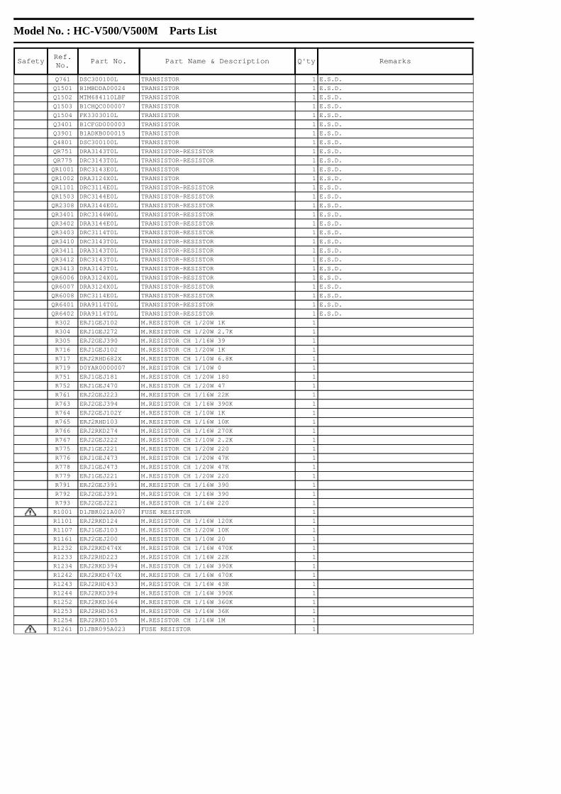
Model No. : HC-V500/V500M Parts List
Safety Ref. No. Part No. Part Name & Description Q'ty Remarks
Q761 DSC300100L TRANSISTOR 1 E.S.D.
Q1501 B1MBDDA00024 TRANSISTOR 1 E.S.D.
Q1502 MTM684110LBF TRANSISTOR 1 E.S.D.
Q1503 B1CHQC000007 TRANSISTOR 1 E.S.D.
Q1504 FK3303010L TRANSISTOR 1 E.S.D.
Q3401 B1CFGD000003 TRANSISTOR 1 E.S.D.
Q3901 B1ADKB000015 TRANSISTOR 1 E.S.D.
Q4801 DSC300100L TRANSISTOR 1 E.S.D.
QR751 DRA3143T0L TRANSISTOR-RESISTOR 1 E.S.D.
QR775 DRC3143T0L TRANSISTOR-RESISTOR 1 E.S.D.
QR1001 DRC3143E0L TRANSISTOR 1 E.S.D.
QR1002 DRA3124X0L TRANSISTOR 1 E.S.D.
QR1101 DRC3114E0L TRANSISTOR-RESISTOR 1 E.S.D.
QR1503 DRC3144E0L TRANSISTOR-RESISTOR 1 E.S.D.
QR2308 DRA3144E0L TRANSISTOR-RESISTOR 1 E.S.D.
QR3401 DRC3144W0L TRANSISTOR-RESISTOR 1 E.S.D.
QR3402 DRA3144E0L TRANSISTOR-RESISTOR 1 E.S.D.
QR3403 DRC3114T0L TRANSISTOR-RESISTOR 1 E.S.D.
QR3410 DRC3143T0L TRANSISTOR-RESISTOR 1 E.S.D.
QR3411 DRA3143T0L TRANSISTOR-RESISTOR 1 E.S.D.
QR3412 DRC3143T0L TRANSISTOR-RESISTOR 1 E.S.D.
QR3413 DRA3143T0L TRANSISTOR-RESISTOR 1 E.S.D.
QR6006 DRA3124X0L TRANSISTOR-RESISTOR 1 E.S.D.
QR6007 DRA3124X0L TRANSISTOR-RESISTOR 1 E.S.D.
QR6008 DRC3114E0L TRANSISTOR-RESISTOR 1 E.S.D.
QR6401 DRA9114T0L TRANSISTOR-RESISTOR 1 E.S.D.
QR6402 DRA9114T0L TRANSISTOR-RESISTOR 1 E.S.D.
R302 ERJ1GEJ102 M.RESISTOR CH 1/20W 1K 1
R304 ERJ1GEJ272 M.RESISTOR CH 1/20W 2.7K 1
R305 ERJ2GEJ390 M.RESISTOR CH 1/16W 39 1
R716 ERJ1GEJ102 M.RESISTOR CH 1/20W 1K 1
R717 ERJ2RHD682X M.RESISTOR CH 1/10W 6.8K 1
R719 D0YAR0000007 M.RESISTOR CH 1/10W 0 1
R751 ERJ1GEJ181 M.RESISTOR CH 1/20W 180 1
R752 ERJ1GEJ470 M.RESISTOR CH 1/20W 47 1
R761 ERJ2GEJ223 M.RESISTOR CH 1/16W 22K 1
R763 ERJ2GEJ394 M.RESISTOR CH 1/16W 390K 1
R764 ERJ2GEJ102Y M.RESISTOR CH 1/10W 1K 1
R765 ERJ2RHD103 M.RESISTOR CH 1/16W 10K 1
R766 ERJ2RKD274 M.RESISTOR CH 1/16W 270K 1
R767 ERJ2GEJ222 M.RESISTOR CH 1/10W 2.2K 1
R775 ERJ1GEJ221 M.RESISTOR CH 1/20W 220 1
R776 ERJ1GEJ473 M.RESISTOR CH 1/20W 47K 1
R778 ERJ1GEJ473 M.RESISTOR CH 1/20W 47K 1
R779 ERJ1GEJ221 M.RESISTOR CH 1/20W 220 1
R791 ERJ2GEJ391 M.RESISTOR CH 1/16W 390 1
R792 ERJ2GEJ391 M.RESISTOR CH 1/16W 390 1
R793 ERJ2GEJ221 M.RESISTOR CH 1/16W 220 1R1001 D1JBR021A007 FUSE RESISTOR 1
R1101 ERJ2RKD124 M.RESISTOR CH 1/16W 120K 1
R1107 ERJ1GEJ103 M.RESISTOR CH 1/20W 10K 1
R1161 ERJ2GEJ200 M.RESISTOR CH 1/10W 20 1
R1232 ERJ2RKD474X M.RESISTOR CH 1/16W 470K 1
R1233 ERJ2RHD223 M.RESISTOR CH 1/16W 22K 1
R1234 ERJ2RKD394 M.RESISTOR CH 1/16W 390K 1
R1242 ERJ2RKD474X M.RESISTOR CH 1/16W 470K 1
R1243 ERJ2RHD433 M.RESISTOR CH 1/16W 43K 1
R1244 ERJ2RKD394 M.RESISTOR CH 1/16W 390K 1
R1252 ERJ2RKD364 M.RESISTOR CH 1/16W 360K 1
R1253 ERJ2RHD363 M.RESISTOR CH 1/16W 36K 1
R1254 ERJ2RKD105 M.RESISTOR CH 1/16W 1M 1R1261 D1JBR095A023 FUSE RESISTOR 1
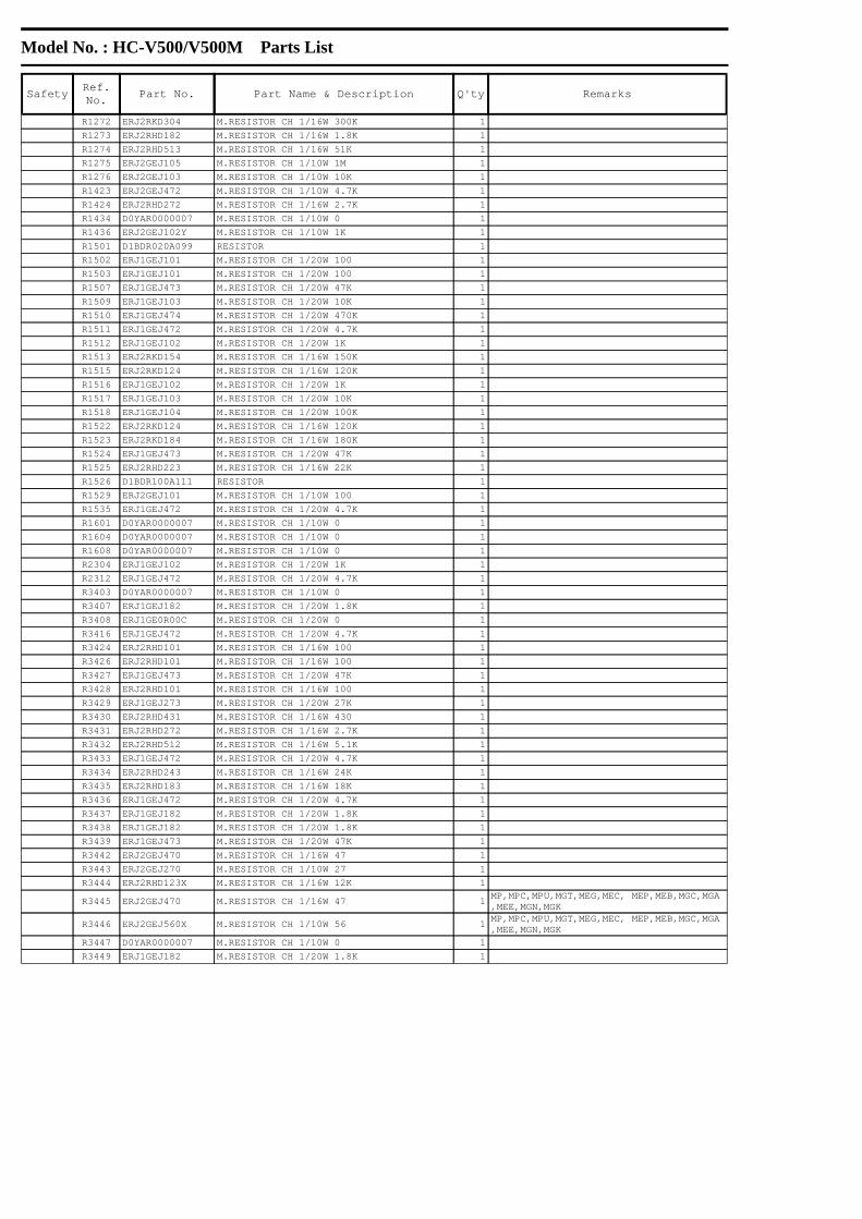
Model No. : HC-V500/V500M Parts List
Safety Ref. No. Part No. Part Name & Description Q'ty Remarks
R1272 ERJ2RKD304 M.RESISTOR CH 1/16W 300K 1
R1273 ERJ2RHD182 M.RESISTOR CH 1/16W 1.8K 1
R1274 ERJ2RHD513 M.RESISTOR CH 1/16W 51K 1
R1275 ERJ2GEJ105 M.RESISTOR CH 1/10W 1M 1
R1276 ERJ2GEJ103 M.RESISTOR CH 1/10W 10K 1
R1423 ERJ2GEJ472 M.RESISTOR CH 1/10W 4.7K 1
R1424 ERJ2RHD272 M.RESISTOR CH 1/16W 2.7K 1
R1434 D0YAR0000007 M.RESISTOR CH 1/10W 0 1
R1436 ERJ2GEJ102Y M.RESISTOR CH 1/10W 1K 1
R1501 D1BDR020A099 RESISTOR 1
R1502 ERJ1GEJ101 M.RESISTOR CH 1/20W 100 1
R1503 ERJ1GEJ101 M.RESISTOR CH 1/20W 100 1
R1507 ERJ1GEJ473 M.RESISTOR CH 1/20W 47K 1
R1509 ERJ1GEJ103 M.RESISTOR CH 1/20W 10K 1
R1510 ERJ1GEJ474 M.RESISTOR CH 1/20W 470K 1
R1511 ERJ1GEJ472 M.RESISTOR CH 1/20W 4.7K 1
R1512 ERJ1GEJ102 M.RESISTOR CH 1/20W 1K 1
R1513 ERJ2RKD154 M.RESISTOR CH 1/16W 150K 1
R1515 ERJ2RKD124 M.RESISTOR CH 1/16W 120K 1
R1516 ERJ1GEJ102 M.RESISTOR CH 1/20W 1K 1
R1517 ERJ1GEJ103 M.RESISTOR CH 1/20W 10K 1
R1518 ERJ1GEJ104 M.RESISTOR CH 1/20W 100K 1
R1522 ERJ2RKD124 M.RESISTOR CH 1/16W 120K 1
R1523 ERJ2RKD184 M.RESISTOR CH 1/16W 180K 1
R1524 ERJ1GEJ473 M.RESISTOR CH 1/20W 47K 1
R1525 ERJ2RHD223 M.RESISTOR CH 1/16W 22K 1
R1526 D1BDR100A111 RESISTOR 1
R1529 ERJ2GEJ101 M.RESISTOR CH 1/10W 100 1
R1535 ERJ1GEJ472 M.RESISTOR CH 1/20W 4.7K 1
R1601 D0YAR0000007 M.RESISTOR CH 1/10W 0 1
R1604 D0YAR0000007 M.RESISTOR CH 1/10W 0 1
R1608 D0YAR0000007 M.RESISTOR CH 1/10W 0 1
R2304 ERJ1GEJ102 M.RESISTOR CH 1/20W 1K 1
R2312 ERJ1GEJ472 M.RESISTOR CH 1/20W 4.7K 1
R3403 D0YAR0000007 M.RESISTOR CH 1/10W 0 1
R3407 ERJ1GEJ182 M.RESISTOR CH 1/20W 1.8K 1
R3408 ERJ1GE0R00C M.RESISTOR CH 1/20W 0 1
R3416 ERJ1GEJ472 M.RESISTOR CH 1/20W 4.7K 1
R3424 ERJ2RHD101 M.RESISTOR CH 1/16W 100 1
R3426 ERJ2RHD101 M.RESISTOR CH 1/16W 100 1
R3427 ERJ1GEJ473 M.RESISTOR CH 1/20W 47K 1
R3428 ERJ2RHD101 M.RESISTOR CH 1/16W 100 1
R3429 ERJ1GEJ273 M.RESISTOR CH 1/20W 27K 1
R3430 ERJ2RHD431 M.RESISTOR CH 1/16W 430 1
R3431 ERJ2RHD272 M.RESISTOR CH 1/16W 2.7K 1
R3432 ERJ2RHD512 M.RESISTOR CH 1/16W 5.1K 1
R3433 ERJ1GEJ472 M.RESISTOR CH 1/20W 4.7K 1
R3434 ERJ2RHD243 M.RESISTOR CH 1/16W 24K 1
R3435 ERJ2RHD183 M.RESISTOR CH 1/16W 18K 1
R3436 ERJ1GEJ472 M.RESISTOR CH 1/20W 4.7K 1
R3437 ERJ1GEJ182 M.RESISTOR CH 1/20W 1.8K 1
R3438 ERJ1GEJ182 M.RESISTOR CH 1/20W 1.8K 1
R3439 ERJ1GEJ473 M.RESISTOR CH 1/20W 47K 1
R3442 ERJ2GEJ470 M.RESISTOR CH 1/16W 47 1
R3443 ERJ2GEJ270 M.RESISTOR CH 1/10W 27 1
R3444 ERJ2RHD123X M.RESISTOR CH 1/16W 12K 1
R3445 ERJ2GEJ470 M.RESISTOR CH 1/16W 47 1 MP,MPC,MPU,MGT,MEG,MEC, MEP,MEB,MGC,MGA ,MEE,MGN,MGK
R3446 ERJ2GEJ560X M.RESISTOR CH 1/10W 56 1 MP,MPC,MPU,MGT,MEG,MEC, MEP,MEB,MGC,MGA ,MEE,MGN,MGK
R3447 D0YAR0000007 M.RESISTOR CH 1/10W 0 1
R3449 ERJ1GEJ182 M.RESISTOR CH 1/20W 1.8K 1

Model No. : HC-V500/V500M Parts List
Safety Ref. No. Part No. Part Name & Description Q'ty Remarks
R3450 D0YAR0000007 M.RESISTOR CH 1/10W 0 1
R3452 ERJ1GEJ473 M.RESISTOR CH 1/20W 47K 1
R3453 ERJ2GEJ103 M.RESISTOR CH 1/10W 10K 1
R3454 ERJ1GEJ473 M.RESISTOR CH 1/20W 47K 1
R3455 ERJ1GEJ473 M.RESISTOR CH 1/20W 47K 1
R3456 ERJ1GEJ102 M.RESISTOR CH 1/20W 1K 1
R3457 ERJ1GEJ103 M.RESISTOR CH 1/20W 10K 1
R3460 ERJ1GEJ473 M.RESISTOR CH 1/20W 47K 1
R3461 ERJ1GEJ104 M.RESISTOR CH 1/20W 100K 1
R3462 ERJ1GEJ473 M.RESISTOR CH 1/20W 47K 1
R3463 ERJ1GEJ104 M.RESISTOR CH 1/20W 100K 1
R3466 ERJ1GEJ473 M.RESISTOR CH 1/20W 47K 1
R3467 ERJ2RKD184 M.RESISTOR CH 1/16W 180K 1
R3468 ERJ2RKD184 M.RESISTOR CH 1/16W 180K 1
R3476 ERJ1GEJ102 M.RESISTOR CH 1/20W 1K 1
R3477 ERJ2GEJ183 M.RESISTOR CH 1/10W 18K 1
R3478 ERJ1GEJ473 M.RESISTOR CH 1/20W 47K 1
R3479 ERJ1GEJ473 M.RESISTOR CH 1/20W 47K 1
R3480 ERJ1GEJ473 M.RESISTOR CH 1/20W 47K 1
R3481 ERJ1GEJ152 M.RESISTOR CH 1/20W 1.5K 1
R3482 ERJ1GEJ153 M.RESISTOR CH 1/20W 15K 1
R3483 ERJ1GEJ153 M.RESISTOR CH 1/20W 15K 1
R3484 ERJ1GEJ104 M.RESISTOR CH 1/20W 100K 1
R3485 ERJ1GEJ101 M.RESISTOR CH 1/20W 100 1
R3486 ERJ2GEJ473Y M.RESISTOR CH 1/10W 47K 1
R3489 ERJ1GEJ101 M.RESISTOR CH 1/20W 100 1
R3490 ERJ1GEJ101 M.RESISTOR CH 1/20W 100 1
R3496 ERJ1GEJ103 M.RESISTOR CH 1/20W 10K 1
R3499 ERJ1GEJ103 M.RESISTOR CH 1/20W 10K 1
R3701 ERJ2GEJ102Y M.RESISTOR CH 1/10W 1K 1
R3711 ERJ1GEJ561 M.RESISTOR CH 1/20W 560 1
R3712 ERJ1GEJ561 M.RESISTOR CH 1/20W 560 1
R3901 ERJ2GEJ470 M.RESISTOR CH 1/16W 47 1
R3902 ERJ2GEJ560X M.RESISTOR CH 1/10W 56 1
R3903 ERJ2GEJ103 M.RESISTOR CH 1/10W 10K 1
R3904 ERJ2GEJ271 M.RESISTOR CH 1/10W 270 1
R3905 ERJ2GEJ331 M.RESISTOR CH 1/16W 330 1
R3906 ERJ2GEJ102Y M.RESISTOR CH 1/10W 1K 1
R3907 ERJ2GEJ102Y M.RESISTOR CH 1/10W 1K 1
R3909 ERJ2GEJ333 M.RESISTOR CH 1/16W 33K 1
R3910 D0GB150JA057 M.RESISTOR CH 1/10W 15 1
R3951 ERJ2GEJ470 M.RESISTOR CH 1/16W 47 1 MP,MPC,MPU,MGT,MEG,MEC, MEP,MEB,MGC,MGA ,MEE,MGN,MGK
R3956 ERJ1GEJ103 M.RESISTOR CH 1/20W 10K 1 MP,MPC,MPU,MGT,MEG,MEC, MEP,MEB,MGC,MGA ,MEE,MGN,MGK
R4802 ERJ1GEJ472 M.RESISTOR CH 1/20W 4.7K 1
R4803 ERJ1GEJ223 M.RESISTOR CH 1/20W 22K 1
R4804 ERJ1GEJ333 M.RESISTOR CH 1/20W 33K 1
R4805 ERJ2GEJ334 M.RESISTOR CH 1/16W 330K 1
R4806 ERJ2GEJ823 M.RESISTOR CH 1/16W 82K 1
R4807 VRE0071E392 M.RESISTOR CH 1/10W 3.9K 1
R4808 ERJ2GEJ334 M.RESISTOR CH 1/16W 330K 1
R4809 ERJ2GEJ823 M.RESISTOR CH 1/16W 82K 1
R4810 VRE0071E392 M.RESISTOR CH 1/10W 3.9K 1
R6001 ERJ2GEJ471 M.RESISTOR CH 1/10W 470 1
R6002 ERJ1GEJ820 M.RESISTOR CH 1/20W 82 1
R6006 ERJ1GEJ102 M.RESISTOR CH 1/20W 1K 1
R6008 ERJ1GEJ820 M.RESISTOR CH 1/20W 82 1
R6009 ERJ1GEJ151 M.RESISTOR CH 1/20W 150 1
R6027 ERJ2RKD750 M.RESISTOR CH 1/16W 75 1
R6028 ERJ2RKD750 M.RESISTOR CH 1/16W 75 1
R6029 ERJ2RKD750 M.RESISTOR CH 1/16W 75 1

Model No. : HC-V500/V500M Parts List
Safety Ref. No. Part No. Part Name & Description Q'ty Remarks
R6030 ERJ2RKD750 M.RESISTOR CH 1/16W 75 1
R6401 ERJ2RHD103 M.RESISTOR CH 1/16W 10K 1
R6402 ERJ2GEJ222 M.RESISTOR CH 1/10W 2.2K 1
R6403 ERJ2GEJ102Y M.RESISTOR CH 1/10W 1K 1
R6405 ERJ2GEJ101 M.RESISTOR CH 1/10W 100 1
R6406 ERJ2RHD202 M.RESISTOR CH 1/16W 2K 1
R6407 ERJ2RHD302 M.RESISTOR CH 1/16W 3K 1
R6408 ERJ2RHD512 M.RESISTOR CH 1/16W 5.1K 1
R6409 ERJ2RHD103 M.RESISTOR CH 1/16W 10K 1
R6410 ERJ2RHD303 M.RESISTOR CH 1/16W 30K 1R6412 D1JBR084A023 FUSE RESISTOR 1
RX3401 D1H82704A024 RESISTOR NETWORKS 1
RX3402 D1H85604A024 RESISTOR NETWORKS 1 MP,MPC,MPU,MGT,MEG,MEC, MEP,MEB,MGC,MGA ,MEE,MGN,MGK
RX3403 D1H84724A024 RESISTOR NETWORKS 1
RX3404 D1H84734A024 RESISTOR NETWORKS 1
RX3405 EXB28V103JX RESISTOR NETWORKS 1
RX3406 EXB28V103JX RESISTOR NETWORKS 1
RX3410 EXB28V103JX RESISTOR NETWORKS 1
RX3901 D1H85604A024 RESISTOR NETWORKS 1
RX3902 EXB28V103JX RESISTOR NETWORKS 1
RX3951 D1H86834A024 RESISTOR NETWORKS 1 MP,MPC,MPU,MGT,MEG,MEC, MEP,MEB,MGC,MGA ,MEE,MGN,MGK
RX6001 EXBN8V100J RESISTOR NETWORKS 1
RX6002 EXBN8V100J RESISTOR NETWORKS 1
S6001 ESE18L62BXFD SWITCH 1
S6002 K0H1BA000580 SWITCH 1
S6401 K0H1BA000580 SWITCH 1
S6402 K0H1BA000580 SWITCH 1
S6403 K0H1BA000580 SWITCH 1
S6404 K0F111A00475 SWITCH 1
VA301 D4ED16R80001 VARISTOR 1
VA1501 D4ED1270A011 VARISTOR 1
VA1502 D4ED1270A011 VARISTOR 1
VA1503 D4ED18R00008 VARISTOR 1
VA1504 D4ED18R00008 VARISTOR 1
VA3902 D4EDY1310001 VARISTOR 1
VA6001 D4ED18R00008 VARISTOR 1
VA6404 D4EDY1310001 VARISTOR 1
X2303 H0J327200085 CRYSTAL OSCILLATOR 1
X3402 H1A6005B0019 CRYSTAL OSCILLATOR 1
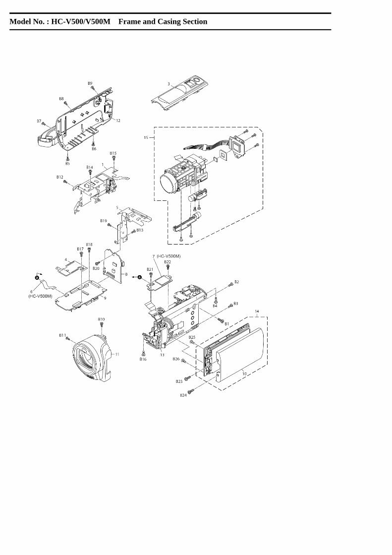
Model No. : HC-V500/V500M Frame and Casing Section

Model No. : HC-V500/V500M Packing Parts and Accessories Section

Model No. : HC-V500/V500M Parts List
Safety Ref. No. Part No. Part Name & Description Q'ty Remarks
1 VXK1997 LENS FRAME UNIT 1
3 VKM9826 TOP CASE 1 (-K,-R)
3 VKM9955 TOP CASE 1 (-S)
4 VXK2002 HEAT RADIATION FRAME UNIT 1
5 VMP0C20 REAR ANGLE 1
6 VWJ2260 RELAY FFC 1 MP,MPC,MPU,MGT,MEG,MEC, MEP,MEB,MGC,MGA ,MEE,MGN,MGK
7 VEP03J60E ESD P.C.B. UNIT (16GB) 1 E.S.D. MP,MPC,MPU,MGT,MEG,MEC, MEP,MEB, MGC,MGA,MEE,MGN,MGK
8 VEP03J50A SD HOLDER P.C.B. UNIT 1 (RTL) E.S.D.
9 VEP03J47A MAIN P.C.B. UNIT 1 (RTL) E.S.D. MP,MPC,MPU,MGT,MEG,MEC, ME P,MEB,MGC,MGA,MEE,MGN,MGK
9 VEP03J47C MAIN P.C.B. UNIT 1 (RTL) E.S.D. PK,PCK,GTK,EG,EF,EC,EP, EB ,GC,GA,EE,GN,GK
10 VYK5J56 LCD CASE(T) UNIT 1 MPK,MPCK,MPUK,MGTK,MEGK, MECK,MEPK,MEBK ,MGCK,MGAK, MEEK,MGNK,MGKK
10 VYK5K71 LCD CASE(T) UNIT 1 MGKR
10 VYK5K63 LCD CASE(T) UNIT 1 PK,PCK,GTK,EGK,EFK,ECK, EPK,EBK,GCK,GAK ,EEK,GNK,GKK
10 VYK5K68 LCD CASE(T) UNIT 1 (-S)
10 VYK5K72 LCD CASE(T) UNIT 1 EGR,EFR,ECR,EPR,GCR,GAR,GKR
11 VYK5J60 FRONT CASE UNIT 1 (-K)
11 VYK5K75 FRONT CASE UNIT 1 (-S)
11 VYK5K76 FRONT CASE UNIT 1 (-R)
12 VYK5J64 SIDE CASE(L) UNIT 1
13 VYK5W47 SIDE CASE(R) UNIT 1 MPK,MPCK,MPUK,MGTK, PK,PCK,GTK
13 VYK5W44 SIDE CASE(R) UNIT 1MEGK,MECK,MEPK,MEBK,MGCK, MGAK,MEEK,MGN K,MGKK,EGK, EFK,ECK,EPK,EBK,GCK,GAK, E EK,GNK,GKK
13 VYK5W46 SIDE CASE(R) UNIT 1 (-S)
13 VYK5W45 SIDE CASE(R) UNIT 1 (-R)
14 VYK5V96 LCD UNIT 1 MPK,MPCK,MPUK,MGTK,MEGK, MECK,MEPK,MEBK ,MGCK,MGAK, MEEK,MGNK,MGKK
14 VYK5V97 LCD UNIT 1 MGKR
14 VYK5V93 LCD UNIT 1 PK,PCK,GTK, EGK,EFK,ECK, EPK,EBK,GCK,GA K,EEK,GNK, GKK
14 VYK5V95 LCD UNIT 1 (-S)
14 VYK5V94 LCD UNIT 1 EGR,EFR,ECR,EPR,GCR,GAR,GKR
15 VXW1350 CAMERA LENS UNIT 1
B1 XQN16+BJ5FJK SCREW 1
B2 XQN16+BJ5FJK SCREW 1
B3 XQN16+BJ5FJK SCREW 1
B4 XQN16+BJ5FJK SCREW 1
B5 XQN16+B4FJK SCREW 1
B6 XQN16+B4FJK SCREW 1
B7 XQN16+B4FJK SCREW 1
B8 XQN16+B4FJK SCREW 1
B9 XQN16+B4FJK SCREW 1
B10 XQN16+B3FN SCREW 1
B11 VHD1919 SCREW 1
B12 VHD1919 SCREW 1
B13 VHD1919 SCREW 1
B14 XQN16+B3FN SCREW 1
B15 XQN16+B3FN SCREW 1
B16 VHD1919 SCREW 1
B17 VHD1919 SCREW 1
B18 VHD1919 SCREW 1
B19 XQN16+BJ5FJK SCREW 1
B20 VHD1919 SCREW 1
B21 VHD1919 SCREW 1
B22 VHD1919 SCREW 1
B23 VHD1688 SCREW 1

Model No. : HC-V500/V500M Parts List
Safety Ref. No. Part No. Part Name & Description Q'ty Remarks
B24 VHD1688 SCREW 1
B25 XQN16+BJ4FJK SCREW 1
B26 XQN16+BJ4FJK SCREW 1
301 K1HY12YY0016 MULTI D/RCA CABLE 1
302 K2KYYYY00201 USB CABLE 1303 K2CA2CA00025 AC CORD W/PLUG 1 MP,MPC,MPU,P,PC303 K2CA2YY00129 AC CORD W/PLUG 1 MGT,GT303 K2CA2YY00130 AC CORD W/PLUG 1 MGK,GK303 K2CT3YY00034 AC CORD W/PLUG 1 MEB,MGC,MGA,EB,GC,GA303 K2CJ2YY00052 AC CORD W/PLUG 1 MGN,GN
303 K2CQ2YY00082 AC CORD W/PLUG 1 MEG,MEC,MEP,MGC,MGA,MEE, EG,EF,EC,EP,GC ,GA,EE
304 VSK0780 AC ADAPTOR 1 MP,MPC,P,PC
304 VSK0781 AC ADAPTOR 1 MPU,MEG,MEC,MEP,MEB,MGC, MGA,MEE,MGN,MG K,EG,EF,EC, EP,EB,GC,GA,EE,GN,GK
304 VSK0714 AC ADAPTOR 1 MGT,GT
305 VFF0890-S CD-ROM 1MP,MGC,MPC,MPU,MGT,MEG, MEC,MEP,MEB,MGA ,MEE,MGN, P,GC,PC,GT,EG,EF,EC,EP, EB,G A,EE,GN
305 VFF0891-S CD-ROM 1 MGK,GK
306 VPF1294 BAG, POLYETHYLENE 1307 VQT4D56 OPERATING INSTRUCTIONS (ENGLISH) 1 P307 VQT3W31 OPERATING INSTRUCTIONS (ENGLISH) 1 MPC,MPU,PC307 VQT3W32 OPERATING INSTRUCTIONS (CANADIAN FRENCH) 1 PC307 VQT3W33 OPERATING INSTRUCTIONS (SPANISH) 1 MPU
307 VQT3W45 OPERATING INSTRUCTIONS (CHINESE(TRADITIONAL)) 1 GT
307 VQT3W34 OPERATING INSTRUCTIONS (GERMAN/TURKISH/ITALIAN/DUTCH) 1 EG
307 VQT3W35 OPERATING INSTRUCTIONS (FRENCH) 1 EG,EF
307 VQT3W36 OPERATING INSTRUCTIONS (SPANISH/PORTUGUESE/SWEDISH/ DANISH) 1 EC
307 VQT3W37 OPERATING INSTRUCTIONS (ENGLISH/POLISH/CZECH/HUNGARIAN) 1 EP
307 VQT3W38 OPERATING INSTRUCTIONS (ENGLISH) 1 EB307 VQT3W39 OPERATING INSTRUCTIONS (ENGLISH) 1 GC307 VQT3W40 OPERATING INSTRUCTIONS (ARABIC/PERSIAN) 1 GC307 VQT3W41 OPERATING INSTRUCTIONS (ENGLISH) 1 GA,GN
307 VQT3W42 OPERATING INSTRUCTIONS (THAI/CHINESE(TRADITIONAL)/HINDI) 1 GA
307 VQT3W43 OPERATING INSTRUCTIONS (RUSSIAN/UKRAINIAN) 1 EE
307 VQT3W44 OPERATING INSTRUCTIONS (CHINESE(SIMPLIFIED)) 1 GK
308 VPG3B42 PACKING CASE 1 MPK
308 VPG3B61 PACKING CASE 1 MPCK
308 VYQ7870 PACKING CASE UNIT 1 MPUK
308 VPG3B62 PACKING CASE 1 MGTK,MEGK,MECK,MEPK,MEBK, MGAK,MEEK,MGN K
308 VPG3B43 PACKING CASE 1 MGCK
308 VYQ7239 PACKING CASE UNIT 1 MGKK
308 VYQ7737 PACKING CASE UNIT 1 MGKR
308 VPG3B44 PACKING CASE 1 PK
308 VPG3B64 PACKING CASE 1 PCK
308 VPG3B65 PACKING CASE 1 GTK,EGK,EFK,ECK,EPK,EBK, GAK,EEK,GNK
308 VYQ7245 PACKING CASE UNIT 1 EGS,EPS,EBS,GAS,EES,GNS
308 VYQ7246 PACKING CASE UNIT 1 EGR,EFR,ECR,EPR,GAR
308 VPG3B45 PACKING CASE 1 GCK
308 VYQ7252 PACKING CASE UNIT 1 GCS
308 VYQ7253 PACKING CASE UNIT 1 GCR
308 VYQ7243 PACKING CASE UNIT 1 GKK
308 VYQ7736 PACKING CASE UNIT 1 GKR
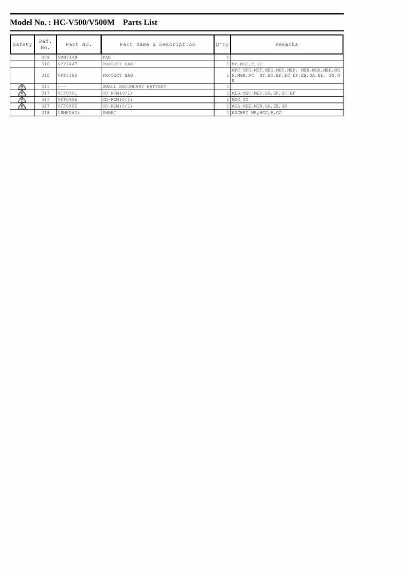
Model No. : HC-V500/V500M Parts List
Safety Ref. No. Part No. Part Name & Description Q'ty Remarks
309 VPN7349 PAD 1
310 VPF1447 PROTECT BAG 1 MP,MGC,P,GC
310 VPF1388 PROTECT BAG 1MPC,MPU,MGT,MEG,MEC,MEP, MEB,MGA,MEE,MG N,MGK,PC, GT,EG,EF,EC,EP,EB,GA,EE, GN,G K
311 --- SMALL SECONDARY BATTERY 1317 VFF0901 CD-ROM(O/I) 1 MEG,MEC,MEP,EG,EF,EC,EP317 VFF0996 CD-ROM(O/I) 1 MGC,GC317 VFF0902 CD-ROM(O/I) 1 MGA,MEE,MGN,GA,EE,GN
318 LSMF0623 SHEET 1 EXCEPT MP,MGC,P,GC


![Model No. HC-W585 HC-W585M HC-V385 - Panasonic USA … · HC-W585 [W585] HC-W585M [W585M] HC-V385 [V385] These operating instructions are designed for use with models , and . Pictures](https://static.cupdf.com/doc/110x72/5f0237ed7e708231d40329d1/model-no-hc-w585-hc-w585m-hc-v385-panasonic-usa-hc-w585-w585-hc-w585m-w585m.jpg)


![HD Видеокамера HC-V770 HC-V760 HC-VX870 HC-VX870M · hc-v770 [v770] Серияv770 / серия [v770] hc-v770m [v770m] hc-v760 [v760] – Данная инструкция](https://static.cupdf.com/doc/110x72/5e697831d35b2b14c40ee20b/hd-hc-v770-hc-v760-hc-vx870-hc-vx870m-hc-v770-v770-v770.jpg)