A D N A N O Z S O Y A N D J E R O M E M I T C H E L L
C S C I B 6 4 9 PA R A L L E L A R C H I T E C T U R E S A N D P R O G R A M M I N G
P R O F. A . C H A U H A N
GRAPHICS PROCESSING UNIT ARCHITECTURES

GRAPHICS PROCESSING UNIT
• Graphics Processing Unit (GPU) • A specialized circuit designed to rapidly manipulate and alter
memory • Accelerate the building of images in a frame buffer intended for
output to a display • GPU -> General Purpose Graphics Processing Unit
(GPGPU) • A general purpose graphics processing unit as a modified form
of stream processor • Transforms the computational power of a modern graphics
accelerator's shader pipeline into general-purpose computing power
2/46 INTRO NVIDIA AMD INTEL CONCLUSION
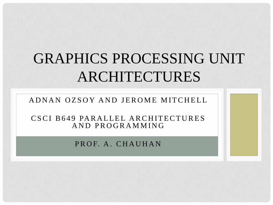
CONVENTIONAL CPU ARCHITECTURE
• Space devoted to control logic instead of ALU
• CPUs are optimized to minimize the latency of a single thread • Can efficiently handle control flow
intensive workloads • Multi level caches used to hide
latency • Limited number of registers due
to smaller number of active threads
• Control logic to reorder execution, provide ILP and minimize pipeline stalls
Perhaad Mistry & Dana Schaa, Northeastern Univ Computer Architecture Research Lab, with Ben Gaster, AMD © 2011
Conventional CPU Block Diagram
Control Logic
ALU
L2 Cache L3 Cach
e
~ 25 GBps
System Memory
A present day multicore CPU could have more than one ALU ( typically < 32) and some of the cache hierarchy is usually shared across cores
3/46 INTRO NVIDIA AMD INTEL CONCLUSION

MODERN GPU ARCHITECTURE
• Generic many core GPU • Less space devoted to control logic
and caches • Large register files to support
multiple thread contexts • Low latency hardware managed
thread switching • Large number of ALU per “core”
with small user managed cache per core
• Memory bus optimized for bandwidth • ~150 GBps bandwidth allows us to
service a large number of ALUs simultaneously
Perhaad Mistry & Dana Schaa, Northeastern Univ Computer Architecture Research Lab, with Ben Gaster, AMD © 2011
On Board System Memory
High Bandwidth bus to ALUs
Simp
le ALUs
Cache
~ 150 GBps
4/46 INTRO NVIDIA AMD INTEL CONCLUSION
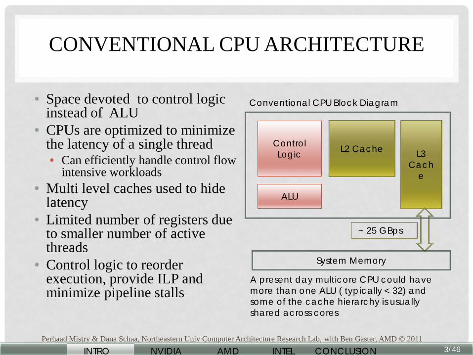
WHAT IS BEHIND SUCH AN EVOLUTION?
• The GPU is specialized for compute-intensive, highly data
parallel computation (exactly what graphics rendering is about) • So, more transistors can be devoted to data processing rather than
data caching and flow control
• The fast-growing video game industry exerts strong economic pressure that forces constant innovation 5
DRAM
Cache
ALU Control
ALU
ALU
ALU
DRAM
CPU GPU
5/46 INTRO NVIDIA AMD INTEL CONCLUSION
GPU VENDORS
6/46 INTRO NVIDIA AMD INTEL CONCLUSION

GPU VENDORS
Courtesy of marketing and research firm Jon Peddie Research (JPR) * May 4 2011, Integrated GPUs, http://jonpeddie.com/press-releases/details/surprising-q1 -results-graphics-shipments-up-10.3-while-pc-shipments-down-5/
7/46 INTRO NVIDIA AMD INTEL CONCLUSION

GPU VENDORS
May 17 2011 , Discrete GPUs, http://jonpeddie.com/publications/add-in-board-report/
Courtesy of marketing and research firm Jon Peddie Research (JPR)
8/46 INTRO NVIDIA AMD INTEL CONCLUSION
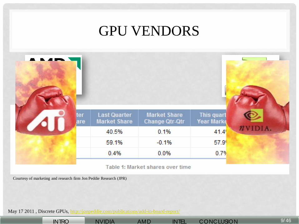
GPU VENDORS
May 17 2011 , Discrete GPUs, http://jonpeddie.com/publications/add-in-board-report/
Courtesy of marketing and research firm Jon Peddie Research (JPR)
9/46 INTRO NVIDIA AMD INTEL CONCLUSION
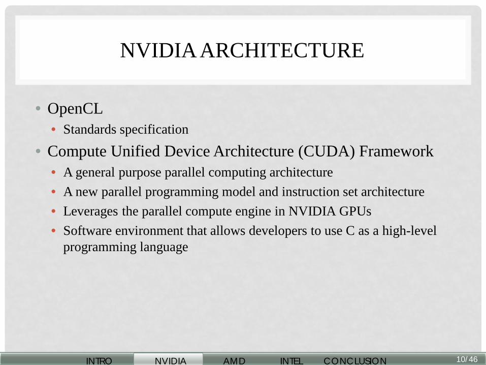
NVIDIA ARCHITECTURE
• OpenCL • Standards specification
• Compute Unified Device Architecture (CUDA) Framework • A general purpose parallel computing architecture • A new parallel programming model and instruction set architecture • Leverages the parallel compute engine in NVIDIA GPUs • Software environment that allows developers to use C as a high-level
programming language
10/46 INTRO NVIDIA AMD INTEL CONCLUSION
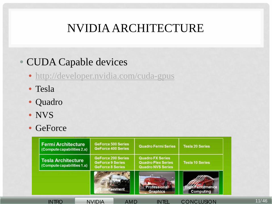
NVIDIA ARCHITECTURE
• CUDA Capable devices • http://developer.nvidia.com/cuda-gpus • Tesla • Quadro • NVS • GeForce
11/46 INTRO NVIDIA AMD INTEL CONCLUSION

TERMINOLOGY REVIEW • Device = GPU = set of multiprocessor • Warp = A scheduling unit of up to 32 threads • Multiprocessor = set of processors & shared memory • Kernel = GPU program • Grid = array of thread blocks that execute a kernel • Thread block = group of SIMD threads that execute a kernel
and can communicate via shared memory
Memory Location Cached Access Who Local Off-chip No Read/write One thread Shared On-chip N/A - resident Read/write All threads in a block Global Off-chip No Read/write All threads + host Constant Off-chip Yes Read All threads + host Texture Off-chip Yes Read All threads + host
12/46 INTRO NVIDIA AMD INTEL CONCLUSION
NVIDIA ARCHITECTURE
• Compute Capability • Specifications and features depend on compute capability • “backward compatible but not forward compatible” • Main differences between 1.x and 2.x
• Increased the number of threads per blocks • Packing up to 462 cores in a single chip • Fermi can run multiple kernels simultaneously • Shared memory has been increased from 16 KB to 48KB • The number of streaming processors in one SM have been increased to 32. • ECC support • support for C++, virtual functions, function pointers, dynamic object
allocation, and C++ exception handling operations • CUDA Programming Guide 4.0 pg. 170-171
13/46 INTRO NVIDIA AMD INTEL CONCLUSION
NVIDIA ARCHITECTURE
• Compute Capability • 1.x (1.0, 1.1, 1.2, 1.3)
• A multiprocessors has 8 CUDA cores • 1 double-precision FP unit for double-precision FP arithmetic operations, • 2 special function units for single-precision FP transcendental functions
(these units can also handle single-precision floating-point multiplications), • 1 warp scheduler.
14/46 INTRO NVIDIA AMD INTEL CONCLUSION
NVIDIA ARCHITECTURE
• Compute Capability • 2.x (2.0, 2.1 – Fermi family)
• For devices of compute capability 2.0: • 32 CUDA cores for integer and FP arithmetic operations, • 4 special function units for single-precision FP
• For devices of compute capability 2.1: • 48 CUDA cores for integer and FP arithmetic operations, • 8 special function units for single-precision FP
• 2 warp schedulers. • GPUDirect
15/46 INTRO NVIDIA AMD INTEL CONCLUSION
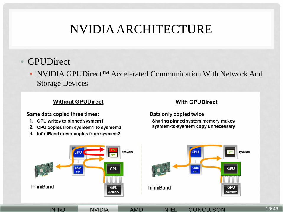
• GPUDirect • NVIDIA GPUDirect™ Accelerated Communication With Network And
Storage Devices
16/46 INTRO NVIDIA AMD INTEL CONCLUSION
NVIDIA ARCHITECTURE
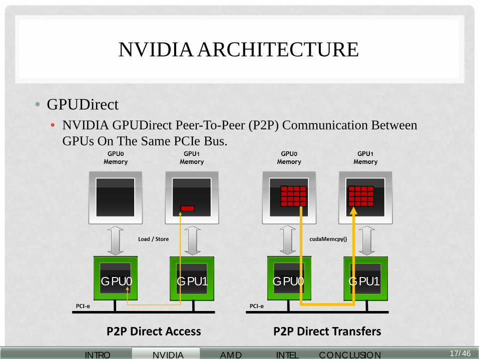
• GPUDirect • NVIDIA GPUDirect Peer-To-Peer (P2P) Communication Between
GPUs On The Same PCIe Bus.
17/46 INTRO NVIDIA AMD INTEL CONCLUSION
NVIDIA ARCHITECTURE
GPU0 GPU1 GPU0 GPU1

G80 HARDWARE IMPLEMENTATION: A SET OF SIMD MULTIPROCESSORS
• The device is a set of 16 multiprocessors
• Each multiprocessor is a set of 32-bit processors with a Single Instruction Multiple Data architecture – shared instruction unit
• At each clock cycle, a multiprocessor executes the same instruction on a group of threads called a warp
• The number of threads in a warp is the warp size
Device
Multiprocessor N
Multiprocessor 2
Multiprocessor 1
Instruction Unit
Processor 1 …
Processor 2 Processor M
18/46 INTRO NVIDIA AMD INTEL CONCLUSION

19/46 INTRO NVIDIA AMD INTEL CONCLUSION
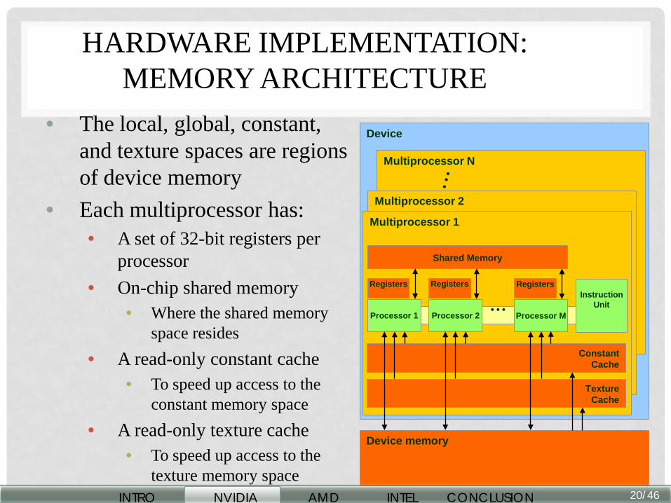
HARDWARE IMPLEMENTATION: MEMORY ARCHITECTURE
• The local, global, constant, and texture spaces are regions of device memory
• Each multiprocessor has: • A set of 32-bit registers per
processor • On-chip shared memory
• Where the shared memory space resides
• A read-only constant cache • To speed up access to the
constant memory space • A read-only texture cache
• To speed up access to the texture memory space 20
Device
Multiprocessor N
Multiprocessor 2
Multiprocessor 1
Device memory
Shared Memory
Instruction Unit
Processor 1
Registers
… Processor 2
Registers
Processor M
Registers
Constant Cache
Texture Cache
20/46 INTRO NVIDIA AMD INTEL CONCLUSION

HARDWARE IMPLEMENTATION: EXECUTION MODEL (REVIEW)
• Each thread block of a grid is split into warps, each gets executed by one multiprocessor (SM) • The device processes only one grid at a time
• Each thread block is executed by one multiprocessor • So that the shared memory space resides in the on-chip shared memory
• A multiprocessor can execute multiple blocks concurrently • Shared memory and registers are partitioned among the threads of all
concurrent blocks • So, decreasing shared memory usage (per block) and register usage (per
thread) increases number of blocks that can run concurrently
21/46 INTRO NVIDIA AMD INTEL CONCLUSION

ACCESS TIMES
• Register – dedicated HW - single cycle • Shared Memory – dedicated HW - single cycle • Local Memory – DRAM, no cache - *slow* • Global Memory – DRAM, no cache - *slow* • Constant Memory – DRAM, cached, 1…10s…100s of cycles,
depending on cache locality • Texture Memory – DRAM, cached, 1…10s…100s of cycles,
depending on cache locality
22/46 INTRO NVIDIA AMD INTEL CONCLUSION
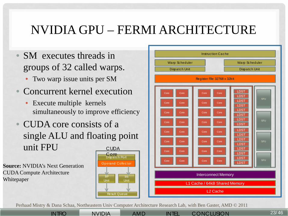
NVIDIA GPU – FERMI ARCHITECTURE
• SM executes threads in groups of 32 called warps. • Two warp issue units per SM
• Concurrent kernel execution • Execute multiple kernels
simultaneously to improve efficiency
• CUDA core consists of a single ALU and floating point unit FPU
Perhaad Mistry & Dana Schaa, Northeastern Univ Computer Architecture Research Lab, with Ben Gaster, AMD © 2011
Source: NVIDIA’s Next Generation CUDA Compute Architecture Whitepaper
Dispatch Port
Operand Collector
FP Unit
Int Unit
Result Queue
CUDA Core
Register File 32768 x 32bit
Warp Scheduler
Core Core
Core Core
Core Core
Core Core
Core Core
Core Core
Core Core
Core Core
Dispatch Unit
Instruction Cache
LDST LDST LDST LDST LDST LDST LDST LDST
LDST LDST LDST LDST LDST LDST LDST LDST
SFU
SFU
SFU
SFU
Interconnect Memory
L1 Cache / 64kB Shared Memory
L2 Cache
Warp Scheduler
Dispatch Unit
Core Core
Core Core
Core Core
Core Core
Core Core
Core Core
Core Core
Core Core
23/46 INTRO NVIDIA AMD INTEL CONCLUSION

NVIDIA MEMORY HIERARCHY
• L1 cache per SM configurable to support shared memory and caching of global memory • 48 KB Shared / 16 KB of L1 cache • 16 KB Shared / 48 KB of L1 cache
• Data shared between work items of a group using shared memory
• Each SM has a 32K register bank • L2 cache (768KB) that services all
operations (load, store and texture) • Unified path to global for loads and stores
Perhaad Mistry & Dana Schaa, Northeastern Univ Computer Architecture Research Lab, with Ben Gaster, AMD © 2011
Shared Memory L1 Cache
L2 Cache
Global Memory
Thread Block
Registers
24/46 INTRO NVIDIA AMD INTEL CONCLUSION
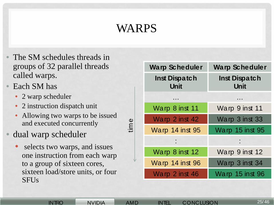
WARPS
Warp Scheduler Warp Scheduler Inst Dispatch
Unit Inst Dispatch
Unit … …
Warp 8 inst 11 Warp 9 inst 11 Warp 2 inst 42 Warp 3 inst 33
Warp 14 inst 95 Warp 15 inst 95 : :
Warp 8 inst 12 Warp 9 inst 12 Warp 14 inst 96 Warp 3 inst 34 Warp 2 inst 46 Warp 15 inst 96
• The SM schedules threads in groups of 32 parallel threads called warps.
• Each SM has • 2 warp scheduler • 2 instruction dispatch unit • Allowing two warps to be issued
and executed concurrently • dual warp scheduler
• selects two warps, and issues one instruction from each warp to a group of sixteen cores, sixteen load/store units, or four SFUs
time
25/46 INTRO NVIDIA AMD INTEL CONCLUSION
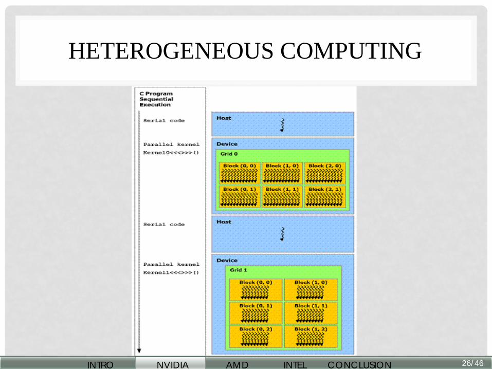
HETEROGENEOUS COMPUTING
26/46 INTRO NVIDIA AMD INTEL CONCLUSION

NVIDIA ARCHITECTURE
• Performance Guidelines • Performance optimization revolves around three basic strategies:
• Maximize parallel execution to achieve maximum utilization; • Optimize memory usage to achieve maximum memory throughput; • Optimize instruction usage to achieve maximum instruction throughput
27/46 INTRO NVIDIA AMD INTEL CONCLUSION
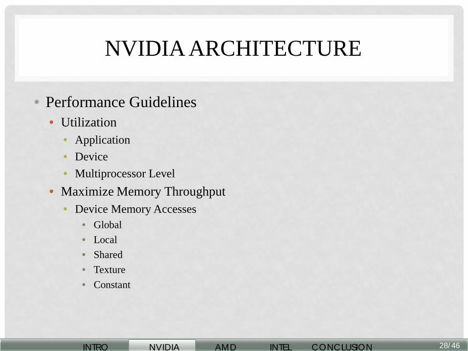
NVIDIA ARCHITECTURE
• Performance Guidelines • Utilization
• Application • Device • Multiprocessor Level
• Maximize Memory Throughput • Device Memory Accesses
• Global • Local • Shared • Texture • Constant
28/46 INTRO NVIDIA AMD INTEL CONCLUSION
NVIDIA ARCHITECTURE
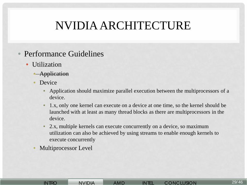
• Performance Guidelines • Utilization
• Application • Device
• Application should maximize parallel execution between the multiprocessors of a device.
• 1.x, only one kernel can execute on a device at one time, so the kernel should be launched with at least as many thread blocks as there are multiprocessors in the device.
• 2.x, multiple kernels can execute concurrently on a device, so maximum utilization can also be achieved by using streams to enable enough kernels to execute concurrently
• Multiprocessor Level
29/46 INTRO NVIDIA AMD INTEL CONCLUSION

NVIDIA ARCHITECTURE
• Performance Guidelines • Utilization
• Application • Device • Multiprocessor Level
• Utilization is therefore directly linked to the number of resident warps. • At every instruction issue time, a warp scheduler selects a warp that is ready to
execute its next instruction, if any. • Hide the latency by having more instructions (more warps)
30/46 INTRO NVIDIA AMD INTEL CONCLUSION

NVIDIA ARCHITECTURE
• Performance Guidelines • Maximum memory throughput
• Minimize data transfers with low bandwidth • Host – Device • Global memory
• Memory access patterns • Global memory • Shared memory
31/46 INTRO NVIDIA AMD INTEL CONCLUSION

NVIDIA ARCHITECTURE
• Performance Guidelines • Memory access patterns
• Global memory resides in device memory and device memory is accessed via 32-, 64-, or 128-byte memory transactions, called segments
• maximize coalescing
32/46 INTRO NVIDIA AMD INTEL CONCLUSION
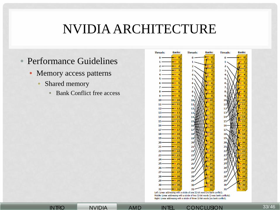
NVIDIA ARCHITECTURE
• Performance Guidelines • Memory access patterns
• Shared memory • Bank Conflict free access
33/46 INTRO NVIDIA AMD INTEL CONCLUSION
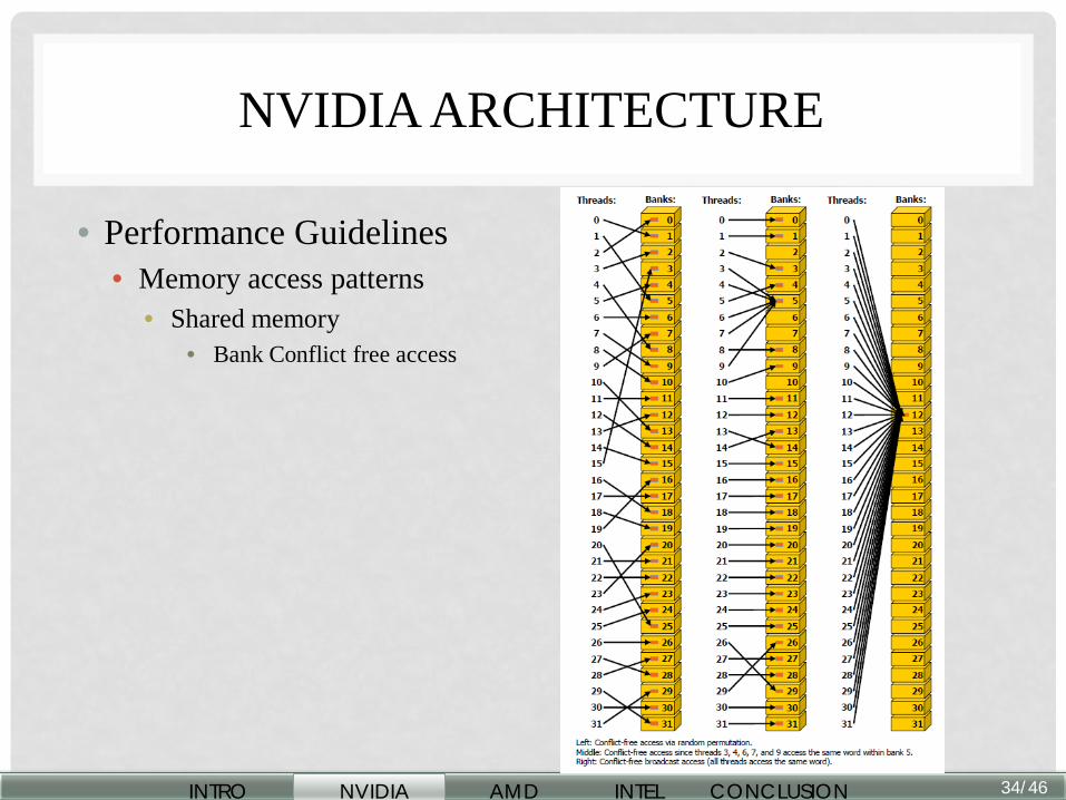
NVIDIA ARCHITECTURE
• Performance Guidelines • Memory access patterns
• Shared memory • Bank Conflict free access
34/46 INTRO NVIDIA AMD INTEL CONCLUSION
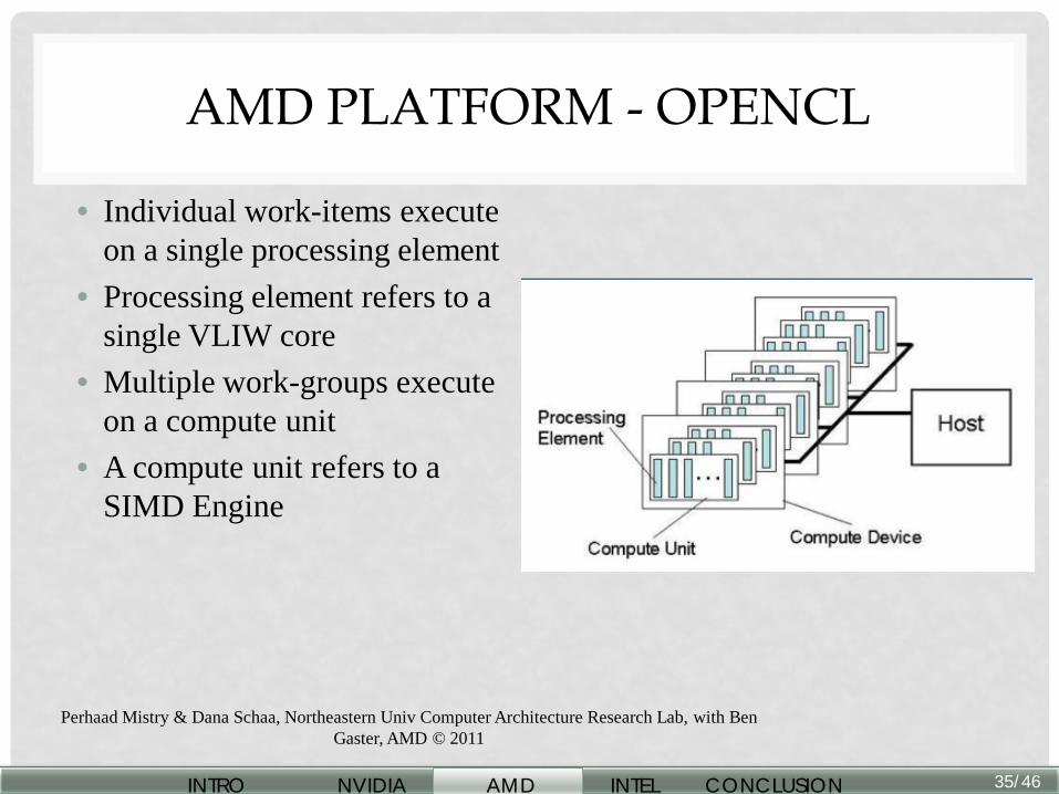
AMD PLATFORM - OPENCL
• Individual work-items execute on a single processing element
• Processing element refers to a single VLIW core
• Multiple work-groups execute on a compute unit
• A compute unit refers to a SIMD Engine
Perhaad Mistry & Dana Schaa, Northeastern Univ Computer Architecture Research Lab, with Ben Gaster, AMD © 2011
35/46 INTRO NVIDIA AMD INTEL CONCLUSION
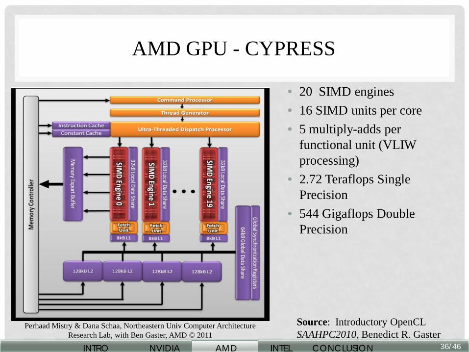
AMD GPU - CYPRESS
• 20 SIMD engines • 16 SIMD units per core • 5 multiply-adds per
functional unit (VLIW processing)
• 2.72 Teraflops Single Precision
• 544 Gigaflops Double Precision
Perhaad Mistry & Dana Schaa, Northeastern Univ Computer Architecture Research Lab, with Ben Gaster, AMD © 2011
Source: Introductory OpenCL SAAHPC2010, Benedict R. Gaster
36/46 INTRO NVIDIA AMD INTEL CONCLUSION
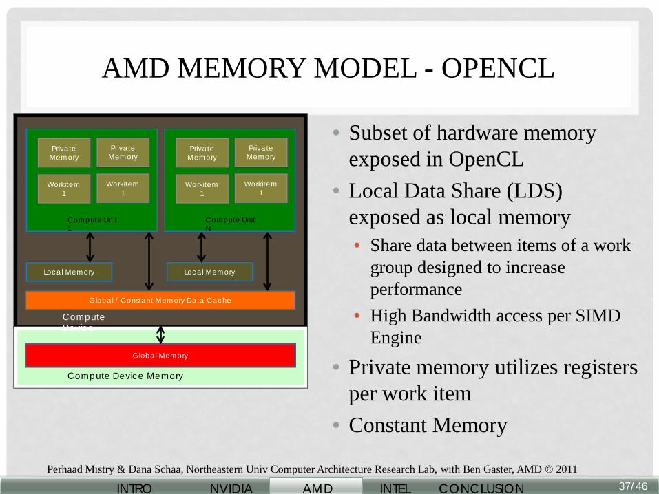
AMD MEMORY MODEL - OPENCL
• Subset of hardware memory exposed in OpenCL
• Local Data Share (LDS) exposed as local memory • Share data between items of a work
group designed to increase performance
• High Bandwidth access per SIMD Engine
• Private memory utilizes registers per work item
• Constant Memory
Global Memory
Private Memory
Workitem 1
Private Memory
Workitem 1
Compute Unit 1
Local Memory
Global / Constant Memory Data Cache
Local Memory
Private Memory
Workitem 1
Private Memory
Workitem 1
Compute Unit N
Compute Device
Compute Device Memory
Perhaad Mistry & Dana Schaa, Northeastern Univ Computer Architecture Research Lab, with Ben Gaster, AMD © 2011 37/46 INTRO NVIDIA AMD INTEL CONCLUSION
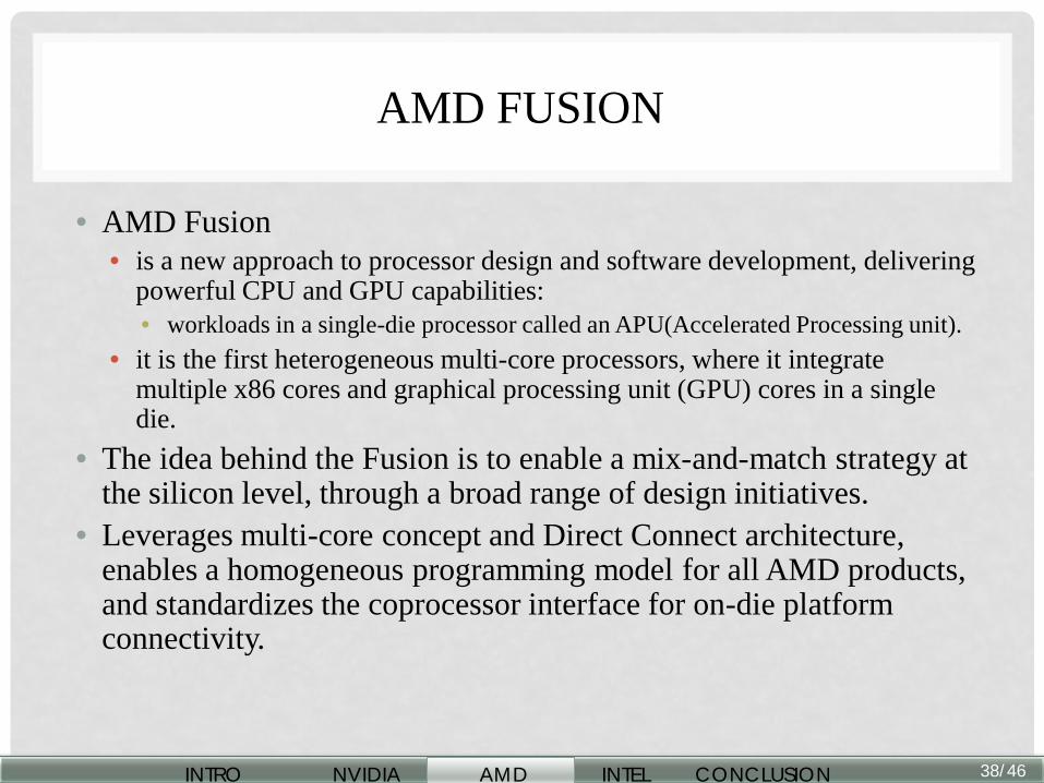
AMD FUSION
• AMD Fusion • is a new approach to processor design and software development, delivering
powerful CPU and GPU capabilities: • workloads in a single-die processor called an APU(Accelerated Processing unit).
• it is the first heterogeneous multi-core processors, where it integrate multiple x86 cores and graphical processing unit (GPU) cores in a single die.
• The idea behind the Fusion is to enable a mix-and-match strategy at the silicon level, through a broad range of design initiatives.
• Leverages multi-core concept and Direct Connect architecture, enables a homogeneous programming model for all AMD products, and standardizes the coprocessor interface for on-die platform connectivity.
38/46 INTRO NVIDIA AMD INTEL CONCLUSION
WHAT IS AN APU?
• http://www.youtube.com/watch?v=BihrG7DhhBM
39/46 INTRO NVIDIA AMD INTEL CONCLUSION

INTEL
• Intel GMA • Series of Intel integrated graphics processors built into
various motherboard chip sets. • These integrated graphics products allow a computer to
be built without a separate graphics card, which can reduce cost, power consumption and noise.
• They rely on the computer's main memory for storage • Performance penalty • CPU and GPU access memory over the same bus
• In early 2007, 90% of all PCs sold had integrated graphics.
• Sandy Bridge / Ivy Bridge • The built-in GPU has up to 12 execution units in Sandy
Bridge • Ivy Bridge will have next Generation Intel HD
Graphics with DirectX 11, OpenGL 3.1, and OpenCL 1.1 support.
40/46 INTRO NVIDIA AMD INTEL CONCLUSION
INTEL
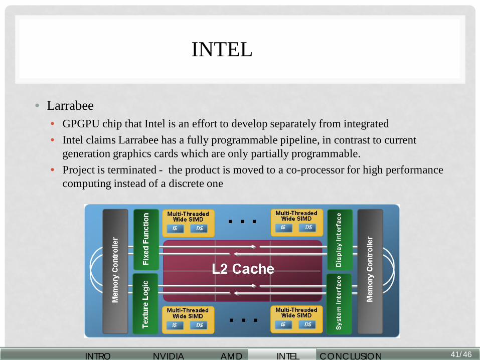
• Larrabee • GPGPU chip that Intel is an effort to develop separately from integrated • Intel claims Larrabee has a fully programmable pipeline, in contrast to current
generation graphics cards which are only partially programmable. • Project is terminated - the product is moved to a co-processor for high performance
computing instead of a discrete one
41/46 INTRO NVIDIA AMD INTEL CONCLUSION

INTEL
42/46 INTRO NVIDIA AMD INTEL CONCLUSION
INTEL
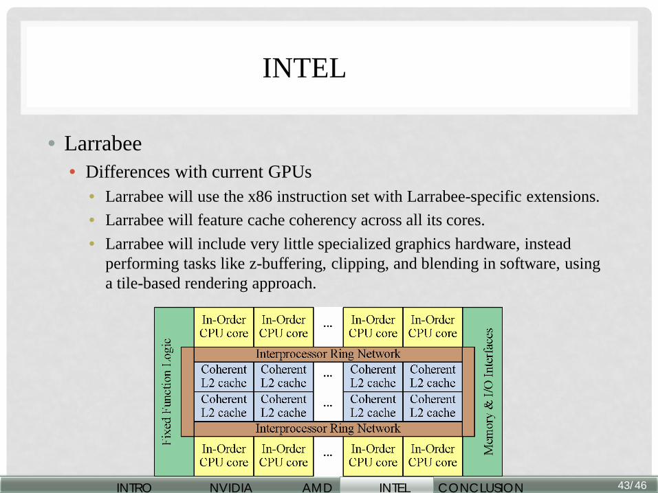
• Larrabee • Differences with current GPUs
• Larrabee will use the x86 instruction set with Larrabee-specific extensions. • Larrabee will feature cache coherency across all its cores. • Larrabee will include very little specialized graphics hardware, instead
performing tasks like z-buffering, clipping, and blending in software, using a tile-based rendering approach.
43/46 INTRO NVIDIA AMD INTEL CONCLUSION

INTEL
• Larrabee • Differences with CPUs
• Larrabee's x86 cores will be based on the much simpler P54C Pentium design with no out-of-order execution
• Each Larrabee core contains a 462-bit vector processing unit, able to process 16 single precision floating point numbers at a time
• Larrabee includes one major fixed-function graphics hardware feature: texture sampling units.
• Larrabee has a 1024-bit (462-bit each way) ring bus for communication between cores and to memory.
• Larrabee includes explicit cache control instructions to reduce cache thrashing
• Each core supports 4-way interleaved multithreading
44/46 INTRO NVIDIA AMD INTEL CONCLUSION
INTEL
• Larrabee • Comparison with Intel GMA
• A discrete GPU • Separate from motherboards • Expected to perform well enough for consideration in the next generation of
video game consoles.
45/46 INTRO NVIDIA AMD INTEL CONCLUSION
CONCLUSIONS
• We went over 3 major GPU vendors • These architectures are on rapid change • It is not a field that reached to a point of maturity for parallel
programming • The limitations include memory accesses, data movement
between host and GPU, architectural dependencies • Knowing the architecture is crucial for achieving high
performance 46/46 INTRO NVIDIA AMD INTEL CONCLUSION

Q & A