International Journal of Microelectronics Engineering (IJME), Vol. 1, No.1 , 2015
51
GENETIC ALGORITHM FOR LEAKAGE REDUCTION
THROUGH IVC USING VERILOG
S.Meera 1, D.Umamaheswari
2
1. PG Vlsi Design, Department of ECE, EBET Group of Institutions,
Kangeyam, Tamilnadu, India.
2. Head of the Department, Department of ECE, EBET Group of Institutions,
Kangeyam, Tamilnadu, India.
ABSTRACT:
VLSI design constraints are always area, power and delay. Power consumption of VLSI has become a leading
design concern with the growth of complexity and density. Leakage power reduces battery life for the entire portable
battery operated device such as mobile phones, laptop and camcoder and so on. Reduction of leakage power is of
peak concern in the present trend of nanotechnology. Many techniques have been projected to reduce the leakage
power consumption, but most of these approaches require the process technology support. Input Vector Control is
one of the approaches used for static power reduction in standby mode. Leakage in a circuit depends on input vector
applied at primary inputs due to stack effect. Minimum leakage vector is the input vector to which a circuit can
suggest a minimum leakage for a certain set of test patterns. This paper presents Minimum Leakage Vector for
various test circuits using genetic algorithm. The algorithm is simulated in Verilog HDL to acquire MLV. Results
explore that heuristic approaches can be considered as better algorithms in finding optimum solution. Another
improvement begins during simulation is that implementation of algorithm in HDL converges in lesser number of
iterations with runtime savings compared to random search method.
Keywords:
Leakage Power, Genetic Algorithm, Input Vector Control, Minimum Leakage Vector, Verilog HDL implementation.
1. INTRODUCTION
As the VLSI technology and supply/threshold voltage maintain scaling down, leakage power has develop
into more and most important in the power dissipation of today‟s CMOS circuits. For example, it is
proposed that sub- threshold leakage power can supply as much as 42% of the total power in the 90 nm
process generation [5]. Many techniques thus have been projected recently to reduce the leakage power
consumption. Dual threshold voltage process use devices with higher threshold voltage along non-critical
paths to decrease leakage current while maintaining the performance [2].
Multiple-threshold CMOS (MTCMOS) technique places a high Vth device in sequence with low Vth
circuitry, creating a sleep transistor [4]. Calhoun et al. proposed a methodology to comprise sleep
transistors in MTCMOS [8]. In dynamic threshold MOS (DTMOS) [5], the gate and body are coupled
International Journal of Microelectronics Engineering (IJME), Vol. 1, No.1 , 2015
52
together and the threshold voltage is changed dynamically to suit the operating state of the circuit.
Another technique to dynamically regulate threshold voltages is the variable threshold CMOS(VTCMOS)
[9]. Controlling the body bias voltage to reduce leakage is discussed in [8]. All of these approaches
require the process technology support. Scaling down the technology to nanometer, results in the increase
of sub threshold leakage current exponentially with the reduction of supply voltage(Vdd) and threshold
voltage. Sub threshold leakage current dominates other leakage current components in current CMOS
technologies. Minimizing leakage power in portable devices is the major task to extend the battery life, as
most of the time, portable devices operate in standby mode. Minimizing leakage power in portable
devices is the major task to extend the battery life, as most of the time, portable devices operate in
standby mode.
IVC is a popular approach used for leakage power reduction. IVC is preferred over other approaches as it
is independent of process technology parameters. IVC is based on transistor stacking effect. This
technique involves parking a circuit in minimum leakage state with no performance over head. Minimum
leakage vector (MLV) is the minimum leakage state among set of test inputs. This MLV can be forced in
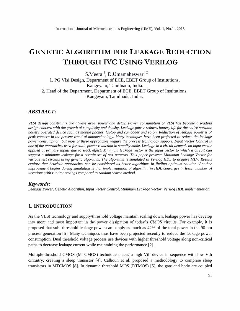
to test circuit using multiplexers (with sleep signal used as a select signal for the MUX)[7]. Sub threshold
Fig.1. Two Input NAND Gate
and gate oxide leakage currents varies with the input vector applied to the CMOS gate[2].
Figure.1 shows two input NAND gate. Due to stacking effect of transistors in NAND gate leakage current
depends on input vector [7]. This leakage depends on number of off transistors connected in the stack.
Table.1 shows leakage currents for all possible input combinations of a two input NAND gate. These
leakage current values of Table.1 [2] and used for future calculations of overall leakage currents of test
circuits.
International Journal of Microelectronics Engineering (IJME), Vol. 1, No.1 , 2015
53
Table.1 presents worst case leakage for 11 combination and best leakage for 00 combination which is the
minimum leakage vector for two input NAND gate. Chen. et al introduced genetic algorithm for
searching MLV with accurate leakage current model [3]. Xiaoying Zhao et al [4] also used genetic
algorithm to solve MLV problem with circuit status difference (CSD) as fitness function to overcome the
problems from the proposed technique of [3].
The same CSD as fitness function along with genetic algorithm to find optimal solution. The algorithm is
implemented in Verilog HDL unlike with „C‟ language as in [4]. HDL implementation of the algorithm
converges in less time towards best solution. In this paper by using Verilog HDL implementation of
genetic algorithm, an innovative attempt is made and succeeded to find optimal solution in fewer number
of iterations compared to random search method. It is also reduces the runtime with leakage power
reduction. The paper is organized as follows. Brief description of genetic algorithm is given in Section II
provides the motivation of this paper and section III and Section IV provides the explanations about
genetic algorithm and fitness function. Section V deals with simulation results and analysis of circuits
designed. Finally, section VI concludes the paper and section VII defines about future scope of this paper.
Table 1: Leakage Currents For Two Input Nand Gate
2. MOTIVATION
IVC utilizes the stacking effect of the circuit where more number off transistor in series reduced the
leakage. In logic circuit leakage is directly describing by means of the input of the gate. It means among
all possible combination some input values offer less leakage than other. Table1 describes the leakage
power dissipation of NAND logic. Data obtained by simulation in Synopsys HSPICE using the 180 nm
TSMC model at 1.8V supply voltage. This is seen from Table 1, changing a logic gate in its minimum
leakage vector (00 as in the case of NAND logic) can reduces leakage by on 92.2% of the Worst Leakage
State WLS (i.e. 11 as in the case of NAND logic). Implementation using HSPICE and other tools taken a
more number of iterations to converge and larger runtime. But implementation of genetic algorithm using
verilog HDL providing better result. In combinational circuit every logic gates are directly or not directly
depends on the output of the previous logic gate input. It is concluded that an exhaustive approach is
Input Power Leakage
Vector Dissp. current(nA)
(W)
00 2.42E-12 37.84 (best)
01 2.61E-11 100.30
10 2.15E-11 95.17
11 3.09E-11 454.5(worst)
International Journal of Microelectronics Engineering (IJME), Vol. 1, No.1 , 2015
54
required to locate a minimum leakage vector for a particular circuit while compared to all of its possible
input combinations.
Steps for finding MLV
Consider node and link as a transistor and an interconnection respectively.
i) Select primary input from its primary value to final value or a threshold value.
ii) Ensure for the transistor which is in OFF states in every path of the graph at a given input.
iii) If above than one transistor having OFF state in a path around no leakage takes place.
iv) This process counts the number of OFF transistor in a circuit at every input sample. And a pattern
which gives the minimum leakage set as a MLV.
v) Calculate leakage of the circuit.
3. GENETIC ALGORITHM TO FIND MLV
Evolutionary algorithms (EAs) are population dependent heuristic optimization algorithms that use
biologically stimulated mechanisms. Best fitness value is the optimum solution after iterating through
number of generation ns [11]. Genetic algorithm is a subclass of evolutionary algorithms inspired by the
biological process of genetics and evolution by creating the population of chromosomes. The algorithm
starts with the initial population represented by set of chromosomes. Fitness is evaluated for each
chromosome in the population. Off springs can be generated by different process steps like selection,
cross over and mutation. Off springs with best fitness values will survive to form future generations.
When stopping criteria is satisfied for the given number of iterations, algorithm gives the optimum
solution. Genetic Algorithm (GA) has the advantage of exploiting historical information to consider on
new search points with expected better performance. It derives its behaviour from a metaphor of normal
selection and natural genetics by the formation of a population of chromosomes.
The pseudo code of our GA is given as follows.
GA ( )
{
chromosome_length=length of primary inputs pop size=100; pc =0.96; pm =0.16; generation=1;
initialize a population of the chromosomes while
CSD reduction between ten generations > 0 do
{
evaluate every chromosome in the population roulette wheel selection to select parents crossover and
mutation to form children produce a new generation of the children
}
generation++
}
International Journal of Microelectronics Engineering (IJME), Vol. 1, No.1 , 2015
55
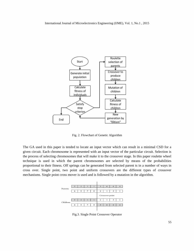
Fig. 2. Flowchart of Genetic Algorithm
The GA used in this paper is tended to locate an input vector which can result in a minimal CSD for a
given circuit. Each chromosome is represented with an input vector of the particular circuit. Selection is
the process of selecting chromosomes that will make it to the crossover stage. In this paper roulette wheel
technique is used in which the parent chromosomes are selected by means of the probabilities
proportional to their fitness. Off springs can be generated from selected parent ts in a number of ways in
cross over. Single point, two point and uniform crossovers are the different types of crossover
mechanisms. Single point cross mover is used and is followed by a mutation in the algorithm.
Fig.3. Single Point Crossover Operator

International Journal of Microelectronics Engineering (IJME), Vol. 1, No.1 , 2015
56
Crossover is the process of comprising the genes of one chromosome with those of another to create
offspring that inherit behaviour of both parents (As shown in Figure 3).
Mutation is the process of shifting bits from one to zero or zero to one in the population. Mutation rate is
considered in the paper as 0.01.In this paper, CSD is used as fitness function, which will be introduced
afterwards. The GA will be terminated when CSD not reduced between 10 generations.
4. CIRCUIT STATUS DIFFERENCE (CSD) AS FITNESS FUNCTION
CIRCUIT STATUS DIFFERENCE (CSD) [4] is the metric used to determine which input will give
minimum leakage current. CSD is considered as fitness function in the paper. It is calculated as the sum
of the products of number of transistors in a gate with its hamming distance. Hamming distance is the
number of bits with which the given vector is differed from its ideal vector.
Some related definitions:
Input state of a cell: For an n-input cell c i in a circuit C, a state s is an n-bit number, with every bit
representing the respective input bit (0 or 1) to the cell. The set of all possible states is represented as Si
for cell ci .
Ideal input state of a cell: For an n-input cell type ci , its ideal state s ideal(i) ∈ Si is the one that results in
the minimum leakage power of ci .
Ideal status of a circuit: When all the cells of the circuit are in their ideal input states, it is supposed that
the circuit was in an ideal status. However, in reality, this ideal status often does not survive because of
the conflicting requirements of cells‟ inputs. Thus our effort would be to find an near to the ideal circuit
status for maximum leakage power reduction.
Circuit status difference: For a input vector v i∈ V, the CSD of v i is defined as
CSD(vi) = ∑ weight (ci) ⋅ HD(si , s ideal(i)) ---(1)
where HD(si,s ideal(i)) is the hamming distance among si and sideal(i) for standard cell c i ∈ C .
Intuitively, the leakage power of a cell is relative to its number of transistors in the cell. The significance
has an additional advantage that it does not change by process technology.
The CSD shows the likelihood of a circuit status under input vector v i and the ideal circuit status. The
lesser the CSD is, the more likely the circuit status under input vi will be to its ideal status.
5. EXPERIMENTAL ANALYSIS
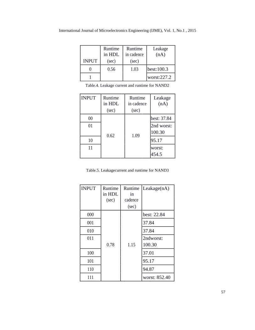
The circuits of INVERTER,NAND2 AND NAND3 were simulated using both cadence and Verilog
HDL.The Leakage current and runtime implementation of INVERTER, NAND2 and NAND3 were
shown in the Table.3 to Table.5.
Table.3. Leakage current and runtime for INVERTER
International Journal of Microelectronics Engineering (IJME), Vol. 1, No.1 , 2015
57
Table.4. Leakage current and runtime for NAND2
INPUT Runtime Runtime Leakage
in HDL in cadence (nA)
(sec) (sec)
00 best: 37.84
01 2nd worst:
0.62
1.09
100.30
10
95.17
11 worst:
454.5
Table.5. Leakagecurrent and runtime for NAND3
INPUT Runtime Runtime Leakage(nA)
in HDL in
(sec) cadence
(sec)
000 best: 22.84
001 37.84
010 37.84
011
0.78
1.15
2ndworst:
100.30
100 37.01
101 95.17
110 94.87
111 worst: 852.40
Runtime Runtime Leakage
in HDL in cadence (nA)
INPUT (sec) (sec)
0 0.56 1.03 best:100.3
1 worst:227.2
International Journal of Microelectronics Engineering (IJME), Vol. 1, No.1 , 2015
58
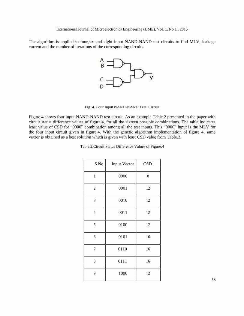
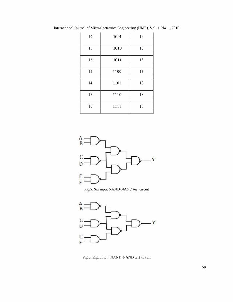
The algorithm is applied to four,six and eight input NAND-NAND test circuits to find MLV, leakage
current and the number of iterations of the corresponding circuits.
Fig. 4. Four Input NAND-NAND Test Circuit
Figure.4 shows four input NAND-NAND test circuit. As an example Table.2 presented in the paper with
circuit status difference values of figure.4, for all the sixteen possible combinations. The table indicates
least value of CSD for “0000” combination among all the test inputs. This “0000” input is the MLV for
the four input circuit given in figure.4. With the genetic algorithm implementation of figure 4, same
vector is obtained as a best solution which is given with least CSD value from Table.2.
Table.2.Circuit Status Difference Values of Figure.4
S.No Input Vector CSD
1 0000 8
2 0001 12
3 0010 12
4 0011 12
5 0100 12
6 0101 16
7 0110 16
8 0111 16
9 1000 12
International Journal of Microelectronics Engineering (IJME), Vol. 1, No.1 , 2015
59
Fig.5. Six input NAND-NAND test circuit
Fig.6. Eight input NAND-NAND test circuit
10 1001 16
11 1010 16
12 1011 16
13 1100 12
14 1101 16
15 1110 16
16 1111 16
International Journal of Microelectronics Engineering (IJME), Vol. 1, No.1 , 2015
60
The Figures 5 and 6 are the six and eight input NANAD-NAND test circuits.The MLV, Leakage current
and number of iterations for the corresponding circuits are shown in table 6.
Table.6. Minimum leakage vectors for test circuits
Test circuit MLV Leakage No.of
current iterations
(nA)
4 input 0000 115.52 10
NAND NAND
circuit
6 input circuit 0000 229.65 20
8 input circuit 0000 278.04 95
Table.6 shows minimum leakage vectors and leakage currents for various test circuits along with number
of iterations. All test circuits can be forced to MLV during standby mode to have minimum leakage
current. These MLVs are obtained from genetic algorithm. HDL implementation of algorithm takes less
number of iterations compared to random methods to give optimum solution. Genetic algorithm with
HDL implementation converges faster as it takes less number of iterations with runtime saving.
Genetic algorithm is implemented in Verilog HDL to find minimum leakage state of the combinational
test circuit. Simulation and synthesis is carried out using Xilinx tool with ISE 9.2i version. Test circuits
can be parked with the respective minimum leakage state during standby mode to reduce leakage power.
This improves backup time of any mobile operated device, which operates most of the time in sleep state
or standby mode.
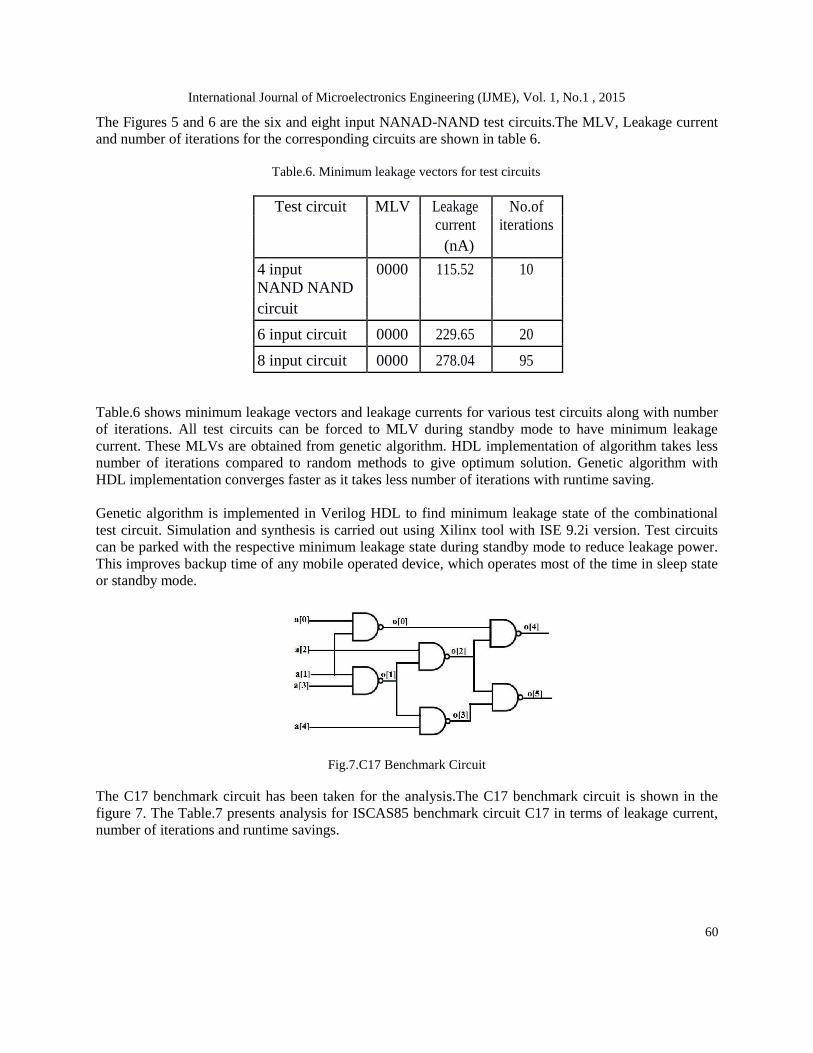
Fig.7.C17 Benchmark Circuit
The C17 benchmark circuit has been taken for the analysis.The C17 benchmark circuit is shown in the
figure 7. The Table.7 presents analysis for ISCAS85 benchmark circuit C17 in terms of leakage current,
number of iterations and runtime savings.
International Journal of Microelectronics Engineering (IJME), Vol. 1, No.1 , 2015
61
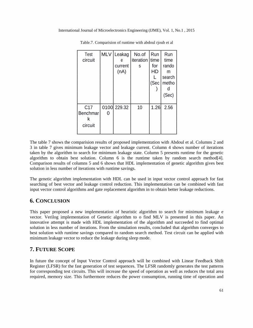
Table.7. Comparision of runtime with abdoul rjoub et al
Test MLV Leakag No.of Run Run circuit e iteration time time
current s for rando (nA) HD m L search (Sec metho ) d
(Sec)
C17 0100 229.32 10 1.26 2.56 Benchmar 0
k
circuit
The table 7 shows the comparision results of proposed implementation with Abdoul et al. Columns 2 and
3 in table 7 gives minimum leakage vector and leakage current. Column 4 shows number of iterations
taken by the algorithm to search for minimum leakage state. Column 5 presents runtime for the genetic
algorithm to obtain best solution. Column 6 is the runtime taken by random search method[4].
Comparison results of columns 5 and 6 shows that HDL implementation of genetic algorithm gives best
solution in less number of iterations with runtime savings.
The genetic algorithm implementation with HDL can be used in input vector control approach for fast
searching of best vector and leakage control reduction. This implementation can be combined with fast
input vector control algorithms and gate replacement algorithm in to obtain better leakage reductions.
6. CONCLUSION
This paper proposed a new implementation of heuristic algorithm to search for minimum leakage e
vector. Verilog implementation of Genetic algorithm to o find MLV is presented in this paper. An
innovative attempt is made with HDL implementation of the algorithm and succeeded to find optimal
solution in less number of iterations. From the simulation results, concluded that algorithm converges to
best solution with runtime savings compared to random search method. Test circuit can be applied with
minimum leakage vector to reduce the leakage during sleep mode.
7. FUTURE SCOPE
In future the concept of Input Vector Control approach will be combined with Linear Feedback Shift
Register (LFSR) for the fast generation of test sequences. The LFSR randomly generates the test patterns
for corresponding test circuits. This will increase the speed of operation as well as reduces the total area
required, memory size. This furthermore reduces the power consumption, running time of operation and
International Journal of Microelectronics Engineering (IJME), Vol. 1, No.1 , 2015
62
number of iterations. This implementation can be combined with other algorithms like fast input vector
control and gate replacement to obtain better leakage reductions.
REFERENCES [1] Nikhil Jayakumar, Sunil P Khatri, “An Algorithm to Minimize Leakage through Simultaneous Input Vector
Control and Circuit Modification”, IEEE Design Automation conference,DATE07,2007.
[2] Lin Yuan, Gang Qu, “ A combined gate replacement and input vector control approach for leakage current
reduction” , IEEE transactions on very large scale integration (vlsi) systems, vol. 14, no. 2, february 2006
[3] Zhanping chen, Liqiong Wei,Mark johnson,Kaushik Roy, “Estimation of standby leakage power in CMOS
circuits considering Accurate modeling of Transistor stacks”, ACM transactions, international symposium on
Low power electronics and design, ISLPED, pp.239- 244,1998.
[4] Xiaoying Zhao, Jiangfang Yi, Dong Tong, Xu Cheng, “Leakage power reduction for cmos combinational
circuits”, IEEE international conference on solid state and integrated circuit technology,2006.
[5] Abdoul Rjoub, Almotasem Belleah Alajlouni,Hassan Almanasrah, “ A Fast input Vector Control App roach for
subthreshold Leakage power reduction” , IEEE electro technical international conference, MELECON, 2012.
[6] Leicheng, Deming Chen,Martin D.Wong, “ A Fast simultaneous input vector generation and gate replacement
algorithm for leakage reduction”ACM transactions,Vol.13,No.2,April 2008.
[7] Weiiun Hung,YuanXie,Narayanan vijay krishnan,Mohamut kandemir, Mary jane irwan, “Total power
optimization for combinational logic using Genetic algorithms”, journal of signal processing
systems,springer,2010.
[8] Rahul Malhotra, Narinder Sing & Yaduvir Singh,“Genetic Algorithms: Concepts, Design for Optimization of
Process Controllers”, vol.4, No.2, March 2011.
[9] WeiiunHung,YuanXie,Narayanan vijay krishnan,Mohamut kandemir,Mary jane irwan, “Total power
optimization for combinational logic using Genetic algorithms”, journal of signal processing
systems,springer,2010.
[10] D. Duarte, Y. Tsai, N. Vijaykrishnan and M. Irwin, “Evaluating Run-Time Techniques for Leakage Power
Reduction,” Proc. Of 15th Intnl. Conjerence on VLSI Design, pp. 31-38,2002.
[11] F. Gao and J. P. Hayes, “Exact and Heuristic Approaches to Input Vector Control for Leakage Power
Reduction”, in Proc. of ICCAD, pp. 527-532 (2004).
[12] A. Abdollahi, F. Fallah and M. Pedram, “Leakage Current Reduction in CMOS VLSI Circuits by Input Vector
Control”, in IEEE Trans. on VLSI, vol. 12, pp.140-154 (2004).
[13] Mohab Anis, Mohamed Elmasry “Multi-Threshold CMOS Digital Circuits : Managing Leakage Power”,
Springer, October 2003.
[14] D. Blaauw, S. Martin, T.N. Mudge, Krisztia‟n Flautner, “Leakage Current Reduction in VLSI Systems”,
Journal of Circuits, Systems, and Computers 11(6): 621-636 (2002).
[15] R.M. Rao, F. Liu, J.L. Burns, and R.B. Brown, “A Heuristic to Determine Low Leakage Sleep State Vectors for
CMOS Combinational Circuits”, IEEE International Conference on Computer-Aided Design, November 2003.