International Journal of Soft Computing and Engineering (IJSCE)
ISSN: 2231-2307, Volume-2, Issue-3, July 2012
451
Published By:
Blue Eyes Intelligence Engineering
& Sciences Publication Retrieval Number: C0799062312 /2012©BEIESP
FSK Modem using PSoC
Y. Sukanya, Sridivya Pathapati
Abstract: The trend to low-cost distributed data
communications over the switched telephone network has
developed the need to integrate even more functions into a single
device. Until recently, the baseband to pass band (and vice versa)
transformation on the serial data produced by a typical data
terminal relied on expensive and bulky external MODEMS to
perform that function. This paper will describe the
implementation of a single-chip FSK Modem circuit based on a
Programmable System on Chip that integrates a modulator, a
demodulator, filters, timers and a baud-rate generator to
accomplish that transformation. The goal is to demonstrate the
possibilities offered by system-on-chip programmable devices in
specific processing systems, where the costs make the use of
specific integrated circuits unaffordable. A common way of
reducing system costs when low baud rates are acceptable is to
use an FSK modem. The modem is responsible for both the
transmission and reception of the data encoded signal. The
device is capable of transmitting and receiving FSK signals in
simplex, half-duplex and asymmetrical full-duplex modes over
two-wire lines and symmetrical full-duplex signals over four-wire
telephone lines. The programming environment of PSoC i.e., PSoC Designer
Integrated Development Environment will assist in configuring,
source code compiling, building, and debugging the system that
runs from internal memory of the PSoC device.
Keywords: FSK, Modem, PSoC, PWM, Programmable.
I. INTRODUCTION
RECENT advances in programmable devices have
provided a viable solution for rapid prototyping of complex
systems focused primarily on digital programmable devices
such as FPGAs, CPLDs, and reconfigurable processors.
Discrete programmable analog arrays have also been
released as products with limited acceptance due to their
high price/performance ratio. High-volume consumer
applications often make use of a small processor and
peripheral devices that are implemented with a few off-the-
shelf parts, and low analog price/performance ratios.
Integration of programmable analog and digital
peripherals with a microcontroller can facilitate the realization of low-cost single-chip embedded systems.
A configurable mixed-signal microcontroller system
should offer cost-effective support for a very wide range of
applications [1]. Programmable resources can be optimized
to support a target application without the time and cost of
designing a custom application-specific integrated circuit
(ASIC). A high level of silicon efficiency can be achieved
by reconfiguring the programmable resources “on the fly” to implement functionality as needed by the application [2].
Manuscript received on July, 2012.
Y.Sukanya, Department of Electronics and Communications
Engineering, Vignan’s Institute of Information Technology, Duvvada,
Visakhapatnam, Andhra Pradesh, India.
Sridivya Pathapati, Department of Electronics and Communications
Engineering, Vignan's Institute of Information Technology, Duvvada,
Visakhapatnam, Andhra Pradesh, India.
So this paper focuses on the implementation of the
Frequency Shift Keying (FSK) modem through the use of
PSoC focusing on reconfigurable hardware as it provides an
excellent platform for design space exploration of low-
power designs with the reprogramability of software making
the task of finding a power effective solution for an intended
application relatively easy.
A.FSK Generation
In the future our society may require and depend on the
ability to move large volumes of information swiftly
between far distant locations. Many examples exist today of
large companies, banks, and even home hobbyists who daily
transmit and receive digital information either over phone
lines or cable systems. Many people who need to transmit data often employ a device known as a modem.
A modem allows digital information to be translated into
a modulated signal which can be easily transmitted over a
phone line [3]. FSK encodes digital data to be transmitted in
an analog fashion by assigning one frequency to a logical 0
and another frequency to a logical 1[4,5]. Transmitting data
in this manner is a simple, robust and standard method for
communicating over telephone lines and a variety of other
transmission media. In the following article, FSK modem
shall be analyzed with a general description of the modem
system and its environment.
Conventional method of FSK
The classical method of generating the FSK employing
monostable multivibrator, multiplexer and using the external
circuitry is complex in nature thereby increasing the cost
and size in implementation. The distortion can also be
introduced due to the non-linearity effect of the transistors which are used externally on a PCB[6].
Simplified Method of FSK in PSoC
Figure1: Block diagram of the Proposed System
While having the benefits of traditional programmable
devices, this approach is significantly less expensive in terms of die area and overall product cost, making it cost
competitive with traditional microcontroller
implementations.

FSK Modem Using PSoC
452
Published By:
Blue Eyes Intelligence Engineering &
Sciences Publication Retrieval Number: C0799062312 /2012©BEIESP
B. PSoC Architecture Overview
Analysis of microcontroller-based systems for sensors, communications, industrial control, and consumer
applications shaped the basic programmable system-on-chip
(PSoC) architecture. A key innovation in this architecture is
the interaction of the heterogeneous programmable blocks,
allowing for study of tradeoffs between analog and digital
implementations. The analog and digital blocks can be
configured as autonomous processors, providing more
parallelism and processing power than with a single-
threaded approach [7].
Figure2: Schematic view of PSoC architecture
The PSoC architecture is shown in Figure2 [8]. The chip
uses the M8 microcontroller used previously in USB
applications. The on-chip clocking solution enables the
device to function with no external components. The chip
family is fabricated in a silicon–oxide–nitride–oxide–silicon
also (SONOS) CMOS technology, offering speeds up to 24
MHz at 5 V, 12 MHz at 3.3 V, and flash memory sizes to 16 kB. Registers mapped into the input/output (I/O) address
space of the microcontroller are used to configure analog
and digital blocks for a specific function, mode, or
interconnect configuration. The function, mode, or
interconnect of blocks may be reconfigured by writing
configuration information to the registers in each of the
programmable blocks.
Both programmable analog and digital circuits are
designed to support a moderate level of abstraction,
balancing flexibility against cost and performance.
The analog blocks are programmed using a set of four 8-bit registers embedded in each block and mapped into the
microcontroller I/O space. Programming fields are defined
for various multiplexer choices, capacitor sizing, clocking
control, switch configuration, and power levels. The switch
configuration and multiplexer choices were defined with
little encoding to provide maximum flexibility in
configuring the analog functions [7].
The digital programmable blocks are designed to offer an
array of peripheral functions commonly used in
microcontroller applications. A specific set of fixed
functions, such as timers, counters, pulse width modulators
(PWMs), cyclic redundancy check (CRC) blocks, and dead-band generators, can be obtained by configuring the digital
blocks. A second type of digital block can be programmed
to add UART and SPI communications capability [7].
A key difference between the PSOC architecture and
previous microcontroller architectures is in the
configurability and interconnection of these digital resources
[9].
II. DESCRIPTION OF FSK MODEM
The Proposed System represents the Implementation of
FSK modulation and demodulation using PSoC.
A.FSK Modulation
Figure3: Block diagram representation of FSK
Modulation The FSK Signal can be generated by using two PWMs
operating at a multiple of the output frequency. The PWMs
are controlled by simulated FSK data driving the PWM
enable inputs. The simulated FSK data is provided by
UART which outputs a pulse train clocked at the Baud rate.
The baud rate utilized for FSK implementation according to
the operating frequencies 2200Hz and 1200Hz is 300
bit/sec.
Baudrate=System clock/ VC1*VC2*VC3Divider*8
Figure4: Configuring UART in PSoC
PWM_freq1 or PWM2200Hz divides the clock source to
provide a fixed multiple of the output frequency at the
logical 1 frequency, 80*2200 Hz. or 177 KHz.PWM_freq0
or PWM1200HZ divides the clock source to provide a fixed
multiple of the output frequency at the logical 0 frequency,
80*1200 Hz or 96 KHz.
The output of UART is interconnected as the input for
PWM1200Hz and PWM2200Hz. It can be configured in
PSoC as follows:

FSK Modem Using PSoC
453
Published By:
Blue Eyes Intelligence Engineering
& Sciences Publication Retrieval Number: C0799062312 /2012©BEIESP
Figure5: Interconnection of UART
PWM 2200Hz is enabled when the data input is high.
PWM1200Hz has its enable input inverted, so that it runs
when the data input is low and stops when the enable input
is high. With one of the PWM enables inverted, when the
output of one PWM is toggling, the other is static. The
outputs are added together with an exclusive-OR gate. When one input is low and static, the output follows the other
toggling input. Thus, when one of PWM 2200Hz or PWM
1200Hz is static, the output follows the toggling input of the
other PWM. The result is a square wave output PWM with
no interrupts. The XOR is implemented in the LUT (Look-
Up Table) that combines two adjacent digital row outputs.
Figure6: XOR Gate Implementation
The output waveform uses the combined outputs (XORd)
of two blocks, but the clock to the filter can only come from
a single block selected by the analog clock multiplexer. This
signal is derived by using PWM (Filter_clock) configured
according to the frequencies of 1200Hz and 2200Hz, then
using this output as the clock source for the analog column
and PGA.
Figure7: Routing of the Digital FSK output
The digital FSK output can be observed at Port 2_0 and is
externally routed to the input of PGA which enables the use
of additional gain for a wider input dynamic range. The output of the PGA is directed to the input of the Switched
Capacitor Band pass filter which generates the analog FSK
output and the filter output performance mainly depends on
the synchronized over sample clock.
Figure8: Placement of analog user modules in PSoC
Software:
The software required to run this FSK generator is simple
and short. The entire code to operate the FSK modulator is
listed in C. Firstly, the User Modules need to be initialized
and started.
The process of debugging is employed to load this
complete integrated process into CY8C29466-24PXI PSoC
device chip consisting of 16 Digital Blocks and 12 Analog
Blocks . The FSK output can be observed by connecting
Port 0_3 to the oscilloscope.

FSK Modem Using PSoC
454
Published By:
Blue Eyes Intelligence Engineering &
Sciences Publication Retrieval Number: C0799062312 /2012©BEIESP
The final schematic view of FSK Generation in PSoC
Designer is as follows:
Figure9: Schematic view of FSK modulator
B. FSK Demodulator
The proposed system uses demodulator which is the
combination of a simple analog and digital hardware. The
core element in the FSK detector is the correlator, consisting
of a delay line and a multiplier. FSK Detection is performed in CY8C27443-PXI Device.
Figure10: Functional Block diagram of FSK
Demodulator
Digital Buffer:
The switched capacitor analog band pass filter generating
the FSK signal is connected to the comparator which forms
the sine wave to square wave conversion. The band pass
filter's comparator bus output is routed to the digital buffer
(DigBuf) User Module for which the output of the DigBuf is
routed to an output row and the adjacent digital block. This
enables use of the output row logic lookup table (LUT) to implement the XOR
(a) (b)
Figure11: Digital buffer User module a) placement in
PSoC b) Parameter configuration
Correlator Implementation:
The elements of the correlator are easily implemented in
the PSoC device. The time delay function is a simple shift
register, with the length and clock set for the delay required,
and the sample rate high enough to faithfully represent the
waveform.
Figure12: General block diagram of Correlator
The delay line delivers a time-delayed replica of the
source signal. The multiplier multiplies the input signal by this delayed replica. The shift register is a modification of
the pseudo random sequence (PRS) generator user module.
This user module has selectable feedback taps that are
XORed back to the input, normally used to generate a
maximum length digital sequence. For this application, the
polynomial routes the single tap at the end of the shift
register chain back to the PRS input.
Figure13: PRS implementation in PSoC
The PRS is hard-wired to invert the output fed back to the
input using an XOR.The shift register clock is derived from
the 24 MHz system clock. With the delay set to 448 μsec
and a 24-bit shift register, we calculate a delay clock of
fCLK = 1/(448 μs/24) = 53.57 kHz, divided down by a PWM and the VC1 clock. The length of the shift register is
set by selecting the proper tap on the 24-bit PRS using the
Write Polynomial API provided as part of the user module.
In this case, the maximum length is set with dwPoly =
00800000h.
There are two ways to implement the multiplier. One way
is to use an analog modulator. Mathematically equivalent,
and even easier to implement, an Exclusive-OR (XOR) gate
acts as a digital multiplier. The output of the XOR is passed
to the same filter that would be used on the modulator
version. The multiplier output waveform appears as a digital signal with a low duty cycle at fL and a high duty cycle at
fH[11].
FSK Modem Using PSoC
455
Published By:
Blue Eyes Intelligence Engineering
& Sciences Publication Retrieval Number: C0799062312 /2012©BEIESP
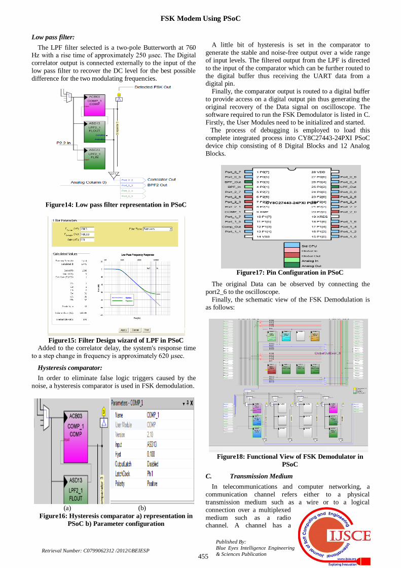
Low pass filter:
The LPF filter selected is a two-pole Butterworth at 760 Hz with a rise time of approximately 250 μsec. The Digital
correlator output is connected externally to the input of the
low pass filter to recover the DC level for the best possible
difference for the two modulating frequencies.
Figure14: Low pass filter representation in PSoC
Figure15: Filter Design wizard of LPF in PSoC
Added to the correlator delay, the system's response time
to a step change in frequency is approximately 620 μsec.
Hysteresis comparator:
In order to eliminate false logic triggers caused by the
noise, a hysteresis comparator is used in FSK demodulation.
(a) (b)
Figure16: Hysteresis comparator a) representation in
PSoC b) Parameter configuration
A little bit of hysteresis is set in the comparator to
generate the stable and noise-free output over a wide range
of input levels. The filtered output from the LPF is directed
to the input of the comparator which can be further routed to
the digital buffer thus receiving the UART data from a digital pin.
Finally, the comparator output is routed to a digital buffer
to provide access on a digital output pin thus generating the
original recovery of the Data signal on oscilloscope. The
software required to run the FSK Demodulator is listed in C.
Firstly, the User Modules need to be initialized and started.
The process of debugging is employed to load this
complete integrated process into CY8C27443-24PXI PSoC
device chip consisting of 8 Digital Blocks and 12 Analog
Blocks.
Figure17: Pin Configuration in PSoC
The original Data can be observed by connecting the
port2_6 to the oscilloscope.
Finally, the schematic view of the FSK Demodulation is
as follows:
Figure18: Functional View of FSK Demodulator in
PSoC
C. Transmission Medium
In telecommunications and computer networking, a
communication channel refers either to a physical
transmission medium such as a wire or to a logical
connection over a multiplexed
medium such as a radio channel. A channel has a

FSK Modem Using PSoC
456
Published By:
Blue Eyes Intelligence Engineering &
Sciences Publication Retrieval Number: C0799062312 /2012©BEIESP
certain capacity for transmitting information, often
measured by its bandwidth in Hz or its data rate in bits per
second [12]. The mode of transmission used here is the
simplex mode by means of a wire for data communication
between the transmitter and receiver.
III. RESULTS:
Input data provided using UART:
Figure19: Selection of the Baud rate from
HyperTerminal
The corresponding output waveforms at the transmitting
section:
Fig (a)
Fig (b)
Figure20: a) Output of PWM1200Hz
b) Output of PWM2200Hz
Baud rate: 15.4b/s
Fig (a)
Fig (b)
Figure21: Character ‘3’ a) Digital FSK Output
b) Analog FSK Output

FSK Modem Using PSoC
457
Published By:
Blue Eyes Intelligence Engineering
& Sciences Publication Retrieval Number: C0799062312 /2012©BEIESP
Fig (a)
Fig (b)
Figure22: a)RS232 Output for character ‘L’
b) FSK Output for character ‘L’
Baud rate 10.1 bit/sec:
Fig (a)
Fig (b)
Figure23: a) Transmitter output for letter ‘i’
b) Transmitter output for letter ‘o’
Baud rate 100.16 bit/sec:
Fig (a)
Fig (b)
Figure24: a) Transmitter output for letter ‘Z’
b) Transmitter output for letter ‘F’
Demodulated Outputs:
Fig (a)
Fig (b)

FSK Modem Using PSoC
458
Published By:
Blue Eyes Intelligence Engineering &
Sciences Publication Retrieval Number: C0799062312 /2012©BEIESP
Fig (c)
Fig (d)
Figure25: a) FSK Detection output for character“f”
b) Demodulated output with respective delay
c) Demodulated output for the letter “u”
d) Demodulated output for the letter “o”
IV. CONCLUSION
This paper demonstrates the possibilities offered by
programmable system on chip which is used for the
implementation of FSK modem. PSoC is an industrial tool,
aiming shorter design to market cycle [10]. The PSoC
architecture integrates heterogeneous abstractions for
programmability and supports dynamic reconfiguration.
With some performance improvement in the future, a mixed
analog /digital programmable IC such as the PSoC is a
promising candidate for designing the low cost modem. This
can be a low cost solution offering fully integrated MCU
with mixed analog, digital peripherals with programmability
and configurability; simple interfaces among peripherals
such as A/D, D/A, PWM, and comparator that can be
configured through design tools; no specific analog or
digital IC knowledge is required for designers[2]. The
programmable approach provides distinct advantages for
mixed-signal systems in rapid prototyping, responsiveness
to late specification changes, exploration of design
alternatives, and support for a wide range of applications
using a single part. This cost-effective approach facilitates
the introduction of programmable analog features to a wider
application space. Final results of this implementation are
very relevant for its precision, flexibility and hardware
reduction.
REFERENCES
1. PSoC Microcontroller Datasheet [Online]. Available:
http://www.cypressmicro.com
2. A. Doboli, and E. Curry,Introduction to Mixed Signal Embedded
Design, San Jose, CA USA :Cypress University Alliance 2008.
3. David R. Smith, "Digital Transmission Systems", Kluwer
International Publishers, 2003, ISBN 1-4020-7587-1
4. Simon Haykin, "Digital Communications", John Wiley & Sons,
1988. ISBN 978-0-471-62947-4.
5. John Proakis, "Digital Communications", 4th edition, McGraw-Hill,
2000. ISBN 0-07-232111-3.
6. Lorraine J. Plaga ,”A General analysis of two FSK modem
demodulators”, IEEE Transactions on Consumer Electronics, Vol.
CE-28, No. 4, November 1982, Consumer Strategic Marketing
Phoenix, Arizona 85062.
7. Monte Mar, Member, IEEE, Bert Sullam, Member, IEEE, and Eric
Blom,”An Architecture for a Configurable Mixed-Signal Device”,
IEEE Journal of Solid-State Circuits, VOL. 38, NO. 3, March 2003.
8. PSoCDeviceDatasheets_CY8C29x66_E, http://www.cypress.com//
9. J. Faura, C. Horton, P. V. Duong, J. Madrenas, M. A. Aguirre, and
J.M. Insenser, “A novel mixed-signal programmable device with on-
chip microprocessor,” in Proc. Custom Integrated Circuits Conf.
(CICC’97), Santa Clara, CA, 1997, pp. 103–106.
10. David Tomanek, DAT Consulting Cons, Pasadena, “What is PSoC”,
Applied Electronics (AE), 2010 International Conference on
California, USA
11. Dennis Seguine, “Simplified FSK Detection”, Application Note,
Cypress Microsystems
12. Channel(communications)
http://en.wikipedia.org/wiki/Communication_channel
AUTHORS PROFILE
Sukanya.Y received her B. Tech Degree in ECE
Department from S.R.K.R Engineering College,
Bheemavaram and obtained her M.Tech degree in
Digital Electronics and Communication Systems from
Gudlavalleru Engineering College. She has eight years
of teaching experience, currently working at Vignan's
Institute of Information Technology, Visakhapatnam as
Associate Professor in Department of ECE. Her Area
of interests are Communication systems and signal
processing.
Sridivya Pathapati obtained her B.Tech degree from
Pydah Engineering College, Visakhapatnam and she is
pursuing M. Tech degree from Vignan's institute of
Information and Technology in the Department of
Electronics & Communications Engineering.
Her Area of interests are Communication systems and
Embedded system design.