Graduate Theses and Dissertations Iowa State University Capstones, Theses andDissertations
2014
Evaluating thermal imaging for identification andcharacterization of solar cell defectsJiahao ChenIowa State University
Follow this and additional works at: https://lib.dr.iastate.edu/etd
Part of the Electrical and Electronics Commons, Mechanics of Materials Commons, and the Oil,Gas, and Energy Commons
This Thesis is brought to you for free and open access by the Iowa State University Capstones, Theses and Dissertations at Iowa State University DigitalRepository. It has been accepted for inclusion in Graduate Theses and Dissertations by an authorized administrator of Iowa State University DigitalRepository. For more information, please contact [email protected].
Recommended CitationChen, Jiahao, "Evaluating thermal imaging for identification and characterization of solar cell defects" (2014). Graduate Theses andDissertations. 13973.https://lib.dr.iastate.edu/etd/13973

Evaluating thermal imaging for identification and characterization of solar cell defects
by
Jiahao Chen
A thesis submitted to the graduate faculty
in partial fulfillment of the requirements for the degree of
MASTER OF SCIENCE
Major: Materials Science and engineering
Program of Study Committee: Kristen P. Constant, Major Professor
Kai-Ming Ho Sumit Chaudhary
Iowa State University
Ames, Iowa
2014
Copyright © Jiahao Chen, 2014. All rights reserved.

ii
TABLE OF CONTENTS
CHAPTER 1 INTRODUCTION ......................................................................... 1
CHAPTER 2 LITERATURE REVIEW ............................................................... 3 2.1 Photovoltaic and Amorphous Silicon Solar Cells .......................................... 3 2.2 Shunts in Solar Cells ...................................................................................... 13 2.3 Infrared Technology in Solar Cell Research and Industry ............................. 18 CHAPTER 3 EXPRIMENTAL METHOD .......................................................... 22 3.1 Camera Calibration ........................................................................................ 23 3.2 Sample Preparation ........................................................................................ 26 3.3 Electrical Measurement and Characterization ............................................... 30 CHAPTER 4 RESULTS AND DISCUSSION ..................................................... 33 4.1 Edge Etching for Sample Preparation ............................................................ 33 4.2 Thermal Imaging ............................................................................................ 36 4.3 Effects of Hot Spot Etching ........................................................................... 40 4.4 Examining the Degradation of Performance after Etching ............................ 46 4.5 Characterization of Solar Cells ...................................................................... 48 CHAPTER 5 FUTURE WORK ............................................................................ 52
REFERENCES .......................................................................................................... 54
ACKNOWLEDGEMENTS ....................................................................................... 57

1
CHAPTER 1
INTRODUCTION
Solar cells have become a primary technology in today’s world for harvesting clean
and renewable energy. Progress has been made towards improving the performance and
quality of solar cells and reducing the cost. Both industry and researchers have done a lot
of work in designing the solar cell structures, finding better materials for fabricating solar
cells and studying the physics of solar cells. However, there remain challenges in
fabrication and materials that degrade the performance of solar cells, one of which is the
existence of shunts. Shunts have been broadly studied and are known to be common
defects in solar cells reducing voltage, current, fill factor and efficiency.
The objective of this research is to develop a method to locate shunts with an IR
camera, quantitatively define the extent to which the shunts affect the efficiency of solar
energy conversion, and explore the nature of shunts. The system chosen for this work is
one of the most common solar cell materials and structures, amorphous silicon solar cells.
In this work, commercially available solar cells are used and prepared for study. IR
inspection is then used to locate the shunts. Then electrical testing is performed to
measure the characteristics of the solar cell. The shunts are then isolated. Then
performance is tested once more to compare with previous data. Microscopy was used to
explore the nature of shunts.
Thesis Organization
The thesis is divided into three main chapters, the literature review, the experimental
method, and results and discussion. The literature review introduces the recent

2
developments in solar cell research and development, basic physics of solar cells and
shunts, and infrared technology for quality control and testing of solar cells. The
experimental approach chapter discusses the details of the sample preparation, testing
tools and conditions, and test procedures. The final chapter reports the results of solar cell
tests and analysis and discussion. Finally, suggestions for future work are made.

3
CHAPTER 2
LITERATURE REVIEW
2.1 Photovoltaic and Amorphous Silicon Solar Cells
A photovoltaic solar cell, which is usually abbreviated as PV, is a device that employs
the photovoltaic effect in semiconducting materials to convert solar energy into electrical
energy. Solar energy is renewable and clean energy, which makes photovoltaics a
promising method to ease the energy crisis without harming the environment. The
photovoltaic effect, [1] first discovered by Alexandre-Edmond Becquerel in 1839, [2] is
the effect that electrons in the valence band are excited into the conduction band by
photons and then electrons in the conduction band are driven into a dissimilar material by
the Galvani potential forming electromotive force. A solar cell can be made of a
semiconductor such as silicon or conducting polymers.
Solar cells are widely studied, their fabrication methods well developed and
performance well characterized. Much of the research aims to develop new solar cell
materials and structures to achieve higher conversion efficiency. Figure 2-1 shows a
recent report from National Renewable Energy Laboratory of solar cell efficiency records
(source: http://www.nrel.gov/ncpv/images/efficiency_chart.jpg). The chart shows the
trend that solar energy conversion has made rapid progress in the recent three decades.
Multi-junction solar cells have as high as 44.4% conversion rate; mono-crystalline silicon
solar cells have also achieved a high conversion efficiency of around 25%; and the other
emerging solar cell technologies are also progressing. All these achievements are positive

4
steps towards making it possible for solar cells to be used as significant source of power
for residential needs.
Figure 2-1: Reported timeline of solar cell energy conversion efficiencies (from National Renewable Energy Laboratory (USA))
2.1.1 Types of Solar Cells
As is illustrated in Figure2-1, solar cells are usually categorized by the materials
comprising the cells. Typically, there are three primary categories of solar cells: silicon
based PV, thin film PV and emerging PV. Silicon solar cells and thin film solar cells are
common and commercially available. This includes expensive mono-crystalline Si, poly-
crystalline Si solar cells and comparatively less expensive thin film solar cells. Other
emerging solar cell technologies are currently under development and mass production
and reliable lifetimes cannot yet be achieved.

5
2.1.1.1 Mono-crystalline Si Solar Cell
Mono-crystalline Si (c-Si) solar cells, also called single-crystal Si solar cells, are
usually made from single crystal silicon wafers with high purity silicon. They have the
advantages of high efficiency and a long lifetime. Most commercial solar modules have
efficiencies of more than 15% and a 20-year expected lifetime. A premium commercial
solar panel from SunPower Inc. can achieve efficiency as high as 20.4%. [3] From this
perspective, this type of solar cell is ideal for residential use. However, because this type
of solar cell is made from single crystalline silicon wafers, it is relatively expensive.
2.1.1.2 Polycrystalline Silicon Solar Cells
Poly-crystalline Si, also known as multi-crystalline silicon (mc-Si), is produced by
casting and cooling molten silicon, followed by a cutting process to make a silicon wafer.
A poly-crystalline silicon solar cell is made from such a silicon wafer. This process is less
expensive than growing mono-crystalline silicon, so the cost of polycrystalline silicon
solar cells is much lower than mono-crystalline Si solar cells. Polycrystalline solar cells
are slightly lower in efficiency. However, the ease of production and resulting lower cost
make them commercially viable. [4]
2.1.1.3 Thin Film Solar Cells
In the 1970s, much research was done on the search for new solar energy materials
and lower-cost solar conversion devices to ease the energy crisis. [5] This resulted in the
development of thin film solar cells, which have been considered as an alternative to
expensive bulk silicon solar cells. After almost 40 years research and development, thin
film solar cells were commercialized. Amorphous silicon (a-Si), Cadmium Telluride

6
(CdTe) and Copper Indium Gallium Selenide (CIS/CIGS) are three types of thin film
solar cell that are now commercially available, as is shown in Figure 2-2.
Thin film solar cells have several advantages, such as simple mass-production, which
makes them cheaper to manufacture, have good flexibility and are lightweight, which
opens up many new potential applications. They can also have comparatively better
performance at high temperatures and in the shade. Low efficiency and fast degradation
are the two main drawbacks of thin-film solar panels, making them less desirable in most
residential applications.
Figure 2-2: Structure of thin film solar cells. (A) CIGS solar cell, (B) CdTe solar cell, (C) Amorphous silicon solar cell [6]
Cadmium telluride solar cells are based on cadmium telluride thin films. CdTe solar
cells are the only thin-film solar panels that have surpassed the cost-efficiency of
crystalline silicon solar panels. The efficiency of solar panels based on cadmium telluride
usually operates in the range of 9-11%. As of May 2014, First Solar has installed over 8
gigawatts (GW) [7] of cadmium telluride thin-film solar panels worldwide. Also, the
company holds the world record for CdTe PV module efficiency of 17.0%. [8]
Copper Indium Gallium Selenide solar cells are based on CuInXGa1-XSe2, which is
a direct bandgap semiconductor. The CIGS absorber can be deposited on a glass or
A B C

7
plastic substrates; due to the high absorption coefficient of the material, the CIGS layer
can be made as a thin film for fabrication of solar cells and is thus flexible, just like
amorphous silicon and CdTe. CIGS solar cells have shown the most potential in terms of
efficiency, and are better than amorphous silicon solar cells in this way. Compared to
CdTe solar cells, CIGS solar cells contain less toxic material and are therefore more eco-
friendly. The efficiency for CIGS solar panels is typically in the range of 10-12%.
Commercialization of CIGS solar cells is comparatively recent, beginning in 2011 in
Germany.
Amorphous silicon solar cells will be discussed in more detail in the next section.
As technology advances, thin-film solar cell efficiencies have increased substantially.
According to Figure 2-1, CIGS and CdTe solar cells have even reached 20.8% and
20.4% respectively. The market for thin-film PV has been growing since 2002. In the
most recent years, market share of thin-film solar cells in the U.S. is close to 5%.
2.1.1.4 Emerging PV Cells
Beyond commercialized solar cells, there are several emerging solar cell technologies
that are being widely studied and developed, among which the most promising are Dye
Sensitized Solar Cells (DSSC) and Organic Solar Cells, also called organic photovoltaics
(OPV).
Dye-sensitized solar cells are an inexpensive alternative to common silicon solar cells
and are based on a semiconductor formed between a photo-sensitized anode and
an electrolyte. Different from silicon solar cells, a DSSC is a
photoelectrochemical system. Modern DSSCs were first developed in 1988 by Brian
O'Regan and Michael Grätzel and the first work on fabrication of DSSCs and
8
measurement of efficiency was published in Nature in 1991. [9] Some characteristics of
DSSC are very promising. DSSC are cost effective and can be fabricated using a simple
conventional roll-printing technique that does not require a clean room or very high
purity materials for the cell itself. DSSCs can also be made semi-flexible and semi-
transparent with the selection of the materials and structure. In practice, there are still
some drawbacks. A number of expensive materials are needed to produce DSSCs,
notably platinum and ruthenium. Also, the required liquid electrolyte limits its
application in some areas with severe weather.
In 2006, Y. Chabal et al. reported a record efficiency of 11.1% for a DSSC [10]. In
2012, a group of scientists announced a new type of DSSC with a solid-state electrolyte
[11], increasing both the efficiency and the lifetime, thereby making it more applicable to
all weather use.
The organic PV cell (OPV) is a type of low cost polymer solar cell that uses
functional polymers for light absorption, conduction and the photovoltaic effects. The
polymer is made of conductive organic polymers or small organic molecules. Cost and
flexibility are the two advantages for OPVs. Materials properties, such as the energy gap,
can be simply modified by changing the molecular composition, which is easier than the
doping process required for silicon semiconductors. The main disadvantages preventing
OPVs from commercialization are low efficiency, low stability and low strength,
compared to inorganic photovoltaic cells.
2.1.2 Amorphous Silicon (a-Si) Solar Cells
Amorphous silicon solar cells are a type of thin-film photovoltaic solar cell. Various
substrates can be used for depositing such thin film layers. Because of the thin film form,
9
only 1% of the silicon used in crystalline silicon solar cells is required in amorphous
silicon solar cells. Also, the substrates required for a-Si solar cell, such as stainless steel
and polyimide films, are inexpensive. As a result, a-Si solar cells are significantly
cheaper than crystalline silicon solar cells.
Amorphous Si solar cells are flexible and light-weight, which allows other
applications beyond mass energy collection. Being light-weight and flexible, a-Si solar
cell can be made into portable devices, such as portable chargers.
2.1.2.1 Amorphous Silicon
Amorphous silicon and solar cells based on amorphous silicon have a long history.
Due to the low output power and low conversion efficiency, initially, this type of solar
cell was only used for small devices such as calculators. With innovations in deposition
technology and multi-junction structures, a-Si solar cells gained potential for more large-
scale applications.
The most common form of amorphous silicon used for solar cells is hydrogenated
amorphous silicon, also known as a-Si:H. Amorphous silicon (a-Si:H) was first deposited
onto substrates in 1969 by R. Chittick. [12] The a-Si:H layers were obtained by reacting
with a SiH4 plasma. Then the process of producing a-Si:H was further developed by W.E.
Spear and co-workers. [13] Plasma enhanced chemical vapor deposition (PECVD) was
introduced to the process, making the deposition more stable and controllable. Doping the
silicon film can also be done by changing the atmosphere gas. Radio Frequency PECVD
(13.56 MHz) is a technique being widely used today for depositing a-Si thin films. [14]
PECVD permits energetic reactions at low temperatures (even 100°C in some cases), due
10
to the formation of cold plasma by electrical ionization rather than thermal ionization, so
that only the electrons are energetic while the ions remain relatively cool.
2.1.2.2 The p-i-n Structure
The typical structure of a p-n junction is not advisable for a-Si solar cells for three
reasons: 1) doping of a-Si is poor; 2) a detrimental effect caused by doping affects the a-
Si layer quality; 3) minority carriers in a-Si have small diffusion lengths. [15] As a result,
a p-i-n structure is used for a-Si solar cell instead of p-n junction structure. Light
absorption and photo-generation of carriers happens in the i-layer, which has a high built-
in electric field to separate the carriers. Typically, the p-layer and n-layer are around tens
of nano meters thick, while the i-layer is around several hundred nano meters. The
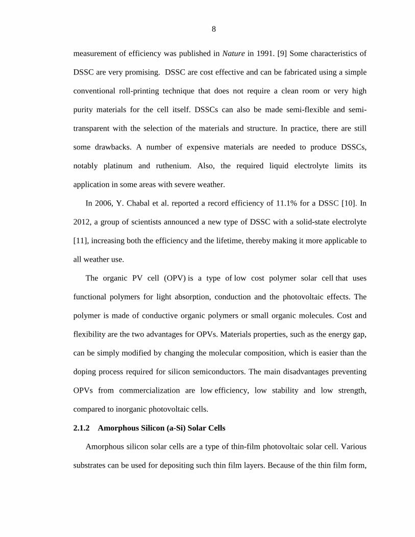
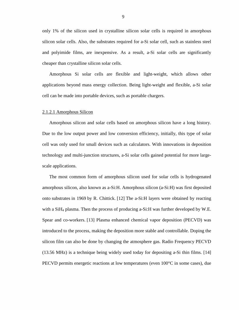
structure of a typical a-Si solar module is shown in Figure 2-3A. Cells are usually
connected in series. Figure 2-3B shows a schematic of the cross-section of an a-Si solar
cell, indicating the position and thickness each layers of an a-Si solar cell.
A
11
Figure 2-3 (A) Structure of an amorphous silicon solar module deposited on glass, (B) schematic of the cross-section of a single junction a-Si solar cell indicating position of each layers. [16]
The first p-i-n a-Si:H solar cell was made by D. Carlson at Princeton. [17] The
introduction of the p-i-n structure greatly increases the efficiency of a-Si solar cells. An
efficiency of 10% had been achieved in a-Si:H solar cells by 1982. [18] However, the
problem of degradation is a main threat to the stability of this type of solar cell. The
efficiency of solar cell will decrease significantly after exposure to light for a certain
time. This light-induced degradation is also called Staebler-Wronsli effect.
2.1.2.3 Multi-junction
As previously mentioned, the efficiency of a-Si:H solar cells is low due to the
Staebler-Wronski effect. One of the methods used today to increase the efficiency is to
build double-junction (tandem) and triple-junction solar cells. Making such multi-
junction solar cell is referred to as “stacking”, which means two or more p-i-n layers of a-
B

12
Si solar cells are stacked one on top of the other. As is shown in Figure 2-4, two cells are
combined by stacking. If the upper cell has a bigger bandgap and the lower cell has
smaller bandgap, this can increase the efficiency. [19]
Figure 2-4: Structure of tandem solar cells where two cells with different band gap are combined [16].
There are two methods to reduce the bandgap of amorphous silicon (1.75 eV). The
first one is to introduce germanium to a-Si:H by alloying. The cell underneath is made of
silicon germanium alloys (a-Si,Ge:H) has an lower bandgap [20][21], which can boost
the efficiency, which has been mentioned above. The other method is to use a two-phase
mixture of amorphous silicon and micro-crystalline silicon (μc-Si) for the bottom cell.
This micro-crystalline silicon has the bandgap of 1.1 eV, similar to wafer-based cells.
This large difference in band gap between the two cells can result in better performance.

13
2.2 Shunts in Solar Cells
Manufacturing does not often produce perfect solar cells, which means that there are
always some defects that affect the performance of solar cells, reducing their efficiency.
One of the most common defects is the existence of shunts.
2.2.1 Solar Cell Theory
A shunt is localized current increase in the dark forward current. Shunts may arise
from materials defects or process induced defects or even improper handling. Figure 2-5
shows a commonly used simplified electrical schematic for a solar cell. It is shown that
equivalent circuit of solar cell has multiple parts, among which the most important
elements are series resistance (RS), shunt resistance (RSH) and the diode.
Figure 2-5: Equivalent circuit model for solar cell
When the solar cell is illuminated, it will create photo-generated current (IL), passing
through the diode (ID) and the shunts (ISH). Thus, the output current can be calculated as:
I = IL−ID−ISH; (1)
The current is controlled by the voltage. The output voltage (V) can also be written
as:
V = Vj - IRS or Vj = V + IRS (2)

14
Where:
Vj = voltage across both diode and resistor RSH
According to Shockley diode equation and Ohm’s law, the current through the diode
and the shun resistor can be expressed by:
(3)
(4)
Where:
I0 = reverse saturation current
n = diode ideality factor
q = elementary charge
k = Boltzmann's constant
T = absolute temperature
Equation (5) can be derived by substituting equation (3) and (4) into equation (1), as
follows:
(5)
From equation (5), it has been shown that there is a relation between output current (I)
and output voltage (V). Though the I cannot be solved for when given a particular V, it is
still physically instructive. If the equation is plotted with certain I0, n, RS, and RSH, the
curve will have the shape shown in Figure 2-6. ISC is short circuit current, which is the
output current (I) when V=0. VOC refers to the open circuit voltage, which is the output
voltage when I=0.

15
Figure 2-6: Illuminated I-V curve of solar cells
2.2.2 Effects of Shunts
Studies show that a low shunt resistance affect the voltages, fill factors, currents and
also the efficiency. [22] Various shunt resistances with a constant series resistance results
in different I-V curves, as shown in Figure 2-7A. A decreased shunt resistance will result
in a voltage decrease. Also, the slope of the curve is significantly affected by the shunt
resistance change, hence resulting in a significant fill factor and output power change.
Shunt resistance is shown to be directly responsible for the fill factors change, as shown
in Figure 2-7B. Low shunt resistance yield low fill factor. Figure 2-7C shows the
relation between output power and shunt resistance. The cell with lower shunt resistance
has lower output power. Since the efficiency equals to output power divided by
illumination intensity, Figure 2-7C shows that efficiency decrease as shunt resistance
decreases. [22]
It can be simply concluded that the presence of shunts in solar cell strongly influences
their performance.

16
Figure 2-7: (A) I-V curve with different Shunt Resistance, (B) Fill Factor with different Shunt Resistance, (C) Power with different Shunt Resistance. [22]
A
B
C
17
2.2.3 Origins of Shunts
Much of the recent research and development in solar cells has focused on higher
efficiency and lower cost. However, the presence of shunts resulting from defects
degrades the efficiency of the solar cells as discussed above. Some defects in the material
will act as recombination centers by introducing different energy levels in the band gap,
and thus reducing the lifetime of free charge carriers and hence efficiency. Typically,
there are several types of shunts in today’s solar cells, caused by material defects such as
dislocations and impurities or processing induced defects.
As indicated by O. Breitenstein etc. in 2004, [23] there are 9 main types of shunts in
silicon solar cells. Six of them are process induced shunts and three of them are materials
induced shunts. It has also been suggested that process induced shunts include linear and
non-linear edge shunts, cracks and Schottky—type shunts within the silicon and scratches
and aluminum contamination at the surface.
For a-Si solar cell, there remain uncertainties about the origin of shunts, types of
shunts and the observed phenomenon of shunt busting. Shunt busting refers to the
observed shunt current reduction when a reverse bias is applied to the cell for a certain
period of time. [36] It was proposed by Sourabh Dongaonkar et al. that in a-Si:H solar
cells, one of the causes of shunts is aluminum contamination in the silicon layer. [24] In
their Al incursion hypothesis, Al diffuses into a-Si and works as a counter-dopant,
converting the p-i-n structure to a p-i-p structure, as shown in Figure 2-8. This
hypothesis also explains the shunt-busting phenomenon, which can be often observed in
a-Si solar cells.

18
Regardless of origin, it remains desirable to detect and characterize shunts in solar
cells either as a quality control measure or in process optimization.
Figure 2-8: Schematics of possible localized shunt structures in a-Si:H solar cells [24]
2.3 Infrared Technology in Solar Cell Research and Industry
Infrared thermal imaging, also called thermography, is a very rapidly evolving field in
research as well as in industry. An IR camera can detect radiation in the infrared range of
the electromagnetic spectrum, roughly 9,000–14,000 nanometers.
Any object above absolute zero will emit infrared radiation according to the black
body radiation law. The characteristics of this radiation can be used to measure
temperature. An IR camera can detect and image the radiation from objects and
variations in temperature of the objects can be observed in this way.
Advancements in IR detection design, optics and electronics have made possible the
use of thermography in various fields in science and industry, such as nondestructive
testing and condition monitoring. Inspection for shunts in solar cells for quality control is
another of its applications.

19
2.3.1 Application of Thermography in Solar Cell Research and Industry
Shunts, imaged in solar cells under bias, were first studied with infrared
thermography in 1990. [25] A reverse bias was applied to the solar cell while monitoring
with an IR camera. Shunts in solar cells are indicated as higher temperature because of
the increased current, and thus are called hot spots. In addition to use in research, IR
cameras are increasingly being used for solar panel quality control and maintenance after
being installed. Figure 2-9 shows thermal imaging with a FLIR brand (FLIR Systems,
Inc.) camera to inspect the hot area or bad modules over large area of solar panels.
Figure 2-9 Thermal images taken by a FLIR P660 camera a solar farm (left) and from the back of a solar module (right) [26]
As shown above, a thermal image can clearly show the areas that are hotter in a solar
panel. Because several shunt types exist in solar cells, hot spots and hot areas can give
some, but not all, information about such shunts, especially in crystalline silicon solar
cells, depending on the shape and location. For example, interconnection problems, not
the problems within the cells, can cause heating of an entire module. Also, bypass diodes
can cause strings of cells to heat up, showing up as a patchwork pattern. Shunts,

20
shadowing and cracks in solar cells appear as hot spots under IR camera. Table 2.1
shows the cause of most types of temperature variation in solar cells.
Table 2-1: List of typical module errors. (Source: ZAE Bayern e.V, Überprüfung der Qualität von Photovoltaik- Modulen mittels Infrarot-Aufnahmen, 2007)
Problems types Example Thermal imaging appearance
Processing induced defects Impurities Hot spot (or cold spot)
Cracks inside Crack-like heating
Damages Cracks Crack-like heating
Cracks inside Partially heated
Shading Pollution,
Bird droppings, Humidity
Hot spot
Bypassing diode Patchwork pattern
Bad interconnection Not connected Whole area hotter
2.3.2 Lock-in Thermography (LIT)
Direct thermal imaging has low spatial resolution when inspecting hot spots under
bias. Thermal blurring is the main cause of such low resolution, which is caused by heat
diffusion in the materials. Lock-in thermography, LIT, invented by P.K. Kuo in 1984 is
an effective way to improve the quality of imaging. [27] Lock-in thermography is an IR
camera-based imaging technique that uses modulated excitation to periodically excite
carriers or apply voltages. Signals obtained from the IR camera are processed with frame
catcher software according to the frequency. With such analysis the sensitivity of the
infrared camera is improved. Thus, the shunts in solar cells can be detected with better
spatial resolution because heat diffusion is suppressed giving LIT the advantage over
traditional direct imaging.

21
In 1999, LIT was used for thermal imaging to detect shunts in solar cells under bias
for the first time. [28] With recent development of technology, LIT can now be used to
image the lifetime distribution, which provided information of VOC, excessive series
resistances and Joule type power loss. [29]
22
CHAPTER 3
EXPERIMENTAL METHODS
The solar panels used for experiments were acquired from PowerFilm, Inc., an Ames,
Iowa company that specializes in a-Si thin film solar cells. Samples provided were from
their typical production runs, some of which were known to have more defects than their
typical product. These solar cells are deposited on a polyimide substrate, which is very
flexible. On the polymer substrate is a thin stainless steel layer with an aluminum coating,
which serves as the back electrode. The a-Si layer is deposited on the metal backing. A
transparent conducting oxide (TCO) is deposited on the a-Si layers, serving as the top
electrode.
A typical solar module is of 15.5cm wide and 30cm long with a series of 13
interconnected cells. The total thickness of the module is 1.12mm. Typical VOC and ISC
are higher than 21.5V and 190mA, respectively. Thus for a single cell, the VOC will be
1.65V or higher. Each cell has multiple silver contact fingers. This gives a short circuit
current density of 6mA/cm2.
In order to measure the dark and light I-V response, solar cells were cut into smaller
sections. Large solar panels cannot be measured with precision for light I-V measurement
due to the lack of uniformity of light intensity on the surface. Thus, cutting the cell is
necessary to improve the accuracy of measurements. Edge etching was required to
remove shorts at the edges produced by cutting.
The general procedure of the experiments to identify and characterize shunts is as
follows: 1. Cut samples and etch the edges to prepare for testing; 2. Inspect with an IR
23
camera to locate the hot spots, 3. Test the I-V properties; 4. Etch selected hot spots with
acid to isolate the shunts; 5. Inspect with an IR camera again; 6. Perform electrical testing
and analyze the data.
3.1 IR Camera Calibrations
3.1.1 Camera Specifications
Camera model: FLIR A325SC Infrared Camera;
Lens: FLIR Close-up lens 4X (100μm), (32 × 24mm FOV, ±2.0 mm depth of
field lens);
Resolution: 320 x 230 pixels;
Temporal resolution: 50mK;
Spectral range: 7.5-13.0 μm.
3.1.2 Camera Calibration
An IR camera images and measures the infrared radiation emitted from the sample
being tested, which is also a function of the surface temperature. However, the radiation
received by the camera does not only come from the sample surface but also the
reflection of surroundings, which is influenced by atmosphere absorption. As a result,
there are always several other parameters, besides the real temperature, that affect the
reading of the temperature of the test sample, such as emissivity, reflection radiation and
absorption of the atmosphere. In order to account for these factors, the camera must be
calibrated. To do so, five parameters are measured and entered into the camera software,
including:
• Sample Emissivity
24
• Reflected temperature of sample surface
• Distance between sample and camera
• Relative humidity
• Temperature of the atmosphere
Emissivity is the most important sample parameter, qualifying how much radiation is
emitted compared to a blackbody. Reflected temperature is used to compensate for the
radiation reflected in the sample. Both parameters can be measured with IR camera.
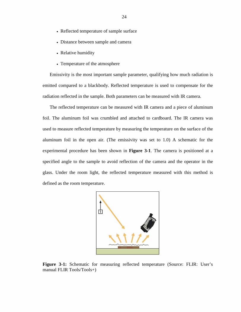
The reflected temperature can be measured with IR camera and a piece of aluminum
foil. The aluminum foil was crumbled and attached to cardboard. The IR camera was
used to measure reflected temperature by measuring the temperature on the surface of the
aluminum foil in the open air. (The emissivity was set to 1.0) A schematic for the
experimental procedure has been shown in Figure 3-1. The camera is positioned at a
specified angle to the sample to avoid reflection of the camera and the operator in the
glass. Under the room light, the reflected temperature measured with this method is
defined as the room temperature.
Figure 3-1: Schematic for measuring reflected temperature (Source: FLIR: User’s manual FLIR Tools/Tools+)

25
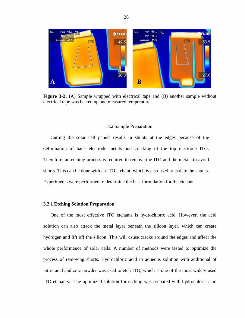
The emissivity of the sample is estimated using electrical tape and a hot plate. The
sample is wrapped with electrical tape and put on the hot plate, which was heated to at
least 45°C. The temperature of the electrical tape was measured afterwards with the
emissivity set to 0.97, a typical value for electrical tape, as shown in Figure 3-2A. Using
this method, the average temperature measured on surface was 45.3°C. After that, the
temperature of the sample is measured in the same way and the emissivity was set to an
appropriate value so that the temperature reads the same as with the electric tape. This
method assumes that the tape and sample reached thermal equilibrium and are at the same
temperature. For example, as is shown in Figure 3-2B, after changing the emissivity to
0.82, the average temperature measured on surface was 45.5°C, approximately the same
temperature obtained in the previous step. In this way, an emissivity of 0.82 was obtained
for an amorphous silicon solar cell. According to literature, [33] the simulated value of
emissivity of a-Si ranges from 0.83-0.96 and the emissivity of ITO is 0.9. Thus, the
emissivity of the solar cells measured by his method was consistent with expected values.
The distance between sample and camera was 10 cm. The atmosphere temperature
was room temperature and the default humidity was used.
With all the parameters obtained and entered, the IR camera software calibration
was run.
26
Figure 3-2: (A) Sample wrapped with electrical tape and (B) another sample without electrical tape was heated up and measured temperature
3.2 Sample Preparation
Cutting the solar cell panels results in shunts at the edges because of the
deformation of back electrode metals and cracking of the top electrode ITO.
Therefore, an etching process is required to remove the ITO and the metals to avoid
shorts. This can be done with an ITO etchant, which is also used to isolate the shunts.
Experiments were performed to determine the best formulation for the etchant.
3.2.1 Etching Solution Preparation
One of the most effective ITO etchants is hydrochloric acid. However, the acid
solution can also attack the metal layer beneath the silicon layer, which can create
hydrogen and lift off the silicon. This will cause cracks around the edges and affect the
whole performance of solar cells. A number of methods were tested to optimize the
process of removing shorts. Hydrochloric acid in aqueous solution with additional of
nitric acid and zinc powder was used to etch ITO, which is one of the most widely used
ITO etchants. The optimized solution for etching was prepared with hydrochloric acid
A B

27
(36.5-38%), alcohol (99.5%) and nitric acid (68.0-70.0%). Table 3-1 shows the recipes of
the acids solutions that were used as ITO etchant to optimize the process.
Table 3-1: Acid solution composition
The solution was designed to allow for etching the top ITO without etching of the
metal layer beneath the silicon layers. Water-based acid solutions resulted in greater
reaction with the metal layer to create hydrogen, which lifted off the silicon layers. Also,
water based acid solution required lower concentration of acids; otherwise concentrated
acids attacked the metal and quickly destroyed the solar cell structure. Solution 1 was too
strong and damaged the silicon layer while the acid attacked the metal. However, when
the solution had a low concentration of acid, the etching speed becomes very slow and
required longer exposure time. This resulted in damage at the edges as the silicon layer
lifted away due to the metal corrosion. Solutions 2 and 3 required long etching time
resulting in unacceptable damage to both the silicon and the metal back. Ethanol based
acid solutions prevented the corrosion of metal and thus less hydrogen was created.
Ethanol based solutions with higher acid concentrations were effective in etching in short
times without metal attack or other damage to the cell. Solution 4 was found to yield
optimum results and was used in these experiments.
Solution type Solution Composition
1 Water-based
acid solution
10ml H2O + 10ml HCl + 5 droplets of HNO3
2 20ml H2O + 10ml HCl + 5 droplets of HNO3 + Zn Powder
3 20ml H2O + 10ml HCl + 5 droplets of HNO3
4 Ethanol-based
acid solution
10ml Ethanol + 10ml HCl + 5 droplets of HNO3
5 20ml Ethanol + 10ml HCl + 5 droplets of HNO3
28
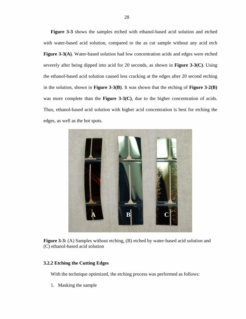
Figure 3-3 shows the samples etched with ethanol-based acid solution and etched
with water-based acid solution, compared to the as cut sample without any acid etch
Figure 3-3(A). Water-based solution had low concentration acids and edges were etched
severely after being dipped into acid for 20 seconds, as shown in Figure 3-3(C). Using
the ethanol-based acid solution caused less cracking at the edges after 20 second etching
in the solution, shown in Figure 3-3(B). It was shown that the etching of Figure 3-2(B)
was more complete than the Figure 3-3(C), due to the higher concentration of acids.
Thus, ethanol-based acid solution with higher acid concentration is best for etching the
edges, as well as the hot spots.
Figure 3-3: (A) Samples without etching, (B) etched by water-based acid solution and (C) ethanol-based acid solution
3.2.2 Etching the Cutting Edges
With the technique optimized, the etching process was performed as follows:
1. Masking the sample
A B C
29
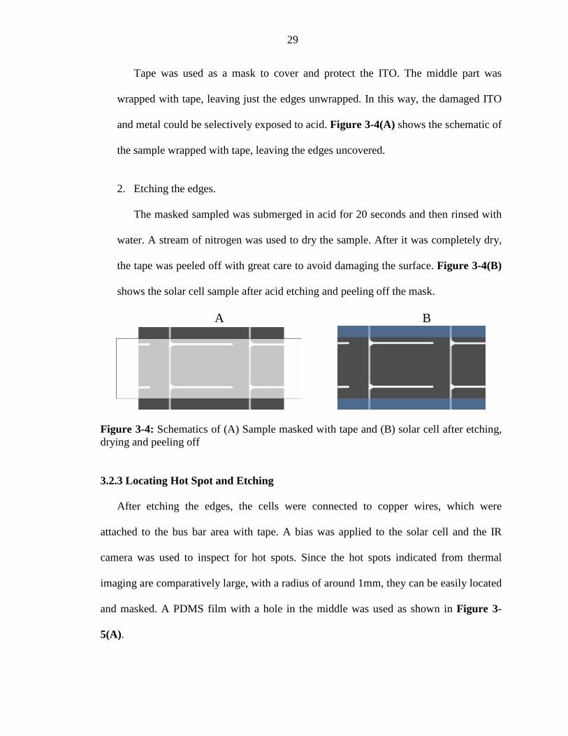
Tape was used as a mask to cover and protect the ITO. The middle part was
wrapped with tape, leaving just the edges unwrapped. In this way, the damaged ITO
and metal could be selectively exposed to acid. Figure 3-4(A) shows the schematic of
the sample wrapped with tape, leaving the edges uncovered.
2. Etching the edges.
The masked sampled was submerged in acid for 20 seconds and then rinsed with
water. A stream of nitrogen was used to dry the sample. After it was completely dry,
the tape was peeled off with great care to avoid damaging the surface. Figure 3-4(B)
shows the solar cell sample after acid etching and peeling off the mask.
A B
Figure 3-4: Schematics of (A) Sample masked with tape and (B) solar cell after etching, drying and peeling off
3.2.3 Locating Hot Spot and Etching
After etching the edges, the cells were connected to copper wires, which were
attached to the bus bar area with tape. A bias was applied to the solar cell and the IR
camera was used to inspect for hot spots. Since the hot spots indicated from thermal
imaging are comparatively large, with a radius of around 1mm, they can be easily located
and masked. A PDMS film with a hole in the middle was used as shown in Figure 3-
5(A).

30
Figure 3-5: Schematics of (A) Sample being inspected and masked for hot spot etching and (B) Sample after etching and drying
After placing the mask, a droplet of acid was applied into the hole in the PDMS. After
etching for 15-20 seconds, the sample was rinsed with water and dried with a stream of
nitrogen, as shown in Figure 3-5(B).
3.3 Electric Measurement and Characterization
3.3.1 Dark I-V Measurement
I-V measurement was conducted with a multi-meter and amplifier controlled by a
LabVIEW program. LabVIEW, product of National Instruments, is software for
measurement or control systems. LabVIEW was also programmed to supply power.
Voltage was swept in 0.2V increments. The multi-meter measured the amplified current
and was computer recorded.
3.3.2 Illuminated I-V Measurement
For a precise measurement of the light I-V curve, a stable light source is required,
which should also closely match the conditions of sunlight. Both the intensity and the
A B

31
spectrum must be matched to a standard. The sun itself can be used for testing solar
cells, but it is difficult to control and varies according to atmospheric conditions and
over the course of the day and the year. These require correction to compare
measurements over time. [31]
The most common alternative is to use an artificial light source that simulates the
sun. The ideal illumination source should have the following features: [32]
• A spatial non uniformity of less than 1%,
• A variation in total irradiance with time of less than 1%,
• Filtered for a given reference spectrum to have a spectral mismatch error of less
than 1%.
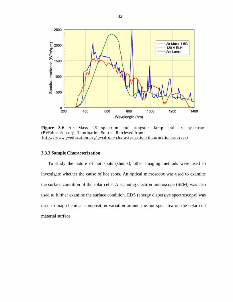
Most solar simulators fit these criteria; however such a simulator was not available
for this study. The spectrum of a tungsten lamp is not as close to solar the spectrum
(A.M. 1.5). But it can also be used for measuring solar cell efficiency, as it has a large
area of overlap with solar spectrum, shown as Figure 3-6.
The light source used here for measuring light I-V curve is of lower intensity. But it is
sufficient for comparison among the samples evaluated.
After the sample was prepared and the light was stabilized, the sample was connected
to lead wires and placed under the light. The position was recorded to ensure uniform
measurement conditions. The following steps were the same as dark I-V measurement
and data was recorded electronically.
32
Figure 3-6 Air Mass 1.5 spectrum and tungsten lamp and arc spectrum (PVEducation.org, Illumination Source, Retrieved from: http://www.pveducation.org/pvcdrom/characterisation/illumination-sources)
3.3.3 Sample Characterization
To study the nature of hot spots (shunts), other imaging methods were used to
investigate whether the cause of hot spots. An optical microscope was used to examine
the surface condition of the solar cells. A scanning electron microscope (SEM) was also
used to further examine the surface condition. EDS (energy dispersive spectroscopy) was
used to map chemical composition variation around the hot spot area on the solar cell
material surface.
33
CHAPTER 4
RESULTS AND DISCUSSION
4.1 Edge Etching for Sample Preparation
Cutting the sample into small pieces was necessary for I-V measurement. When the
solar cell was cut, the metal, silicon, polymer and the top conducting oxide were all
deformed, leading to shorting around the periphery. Etching at the edges is necessary to
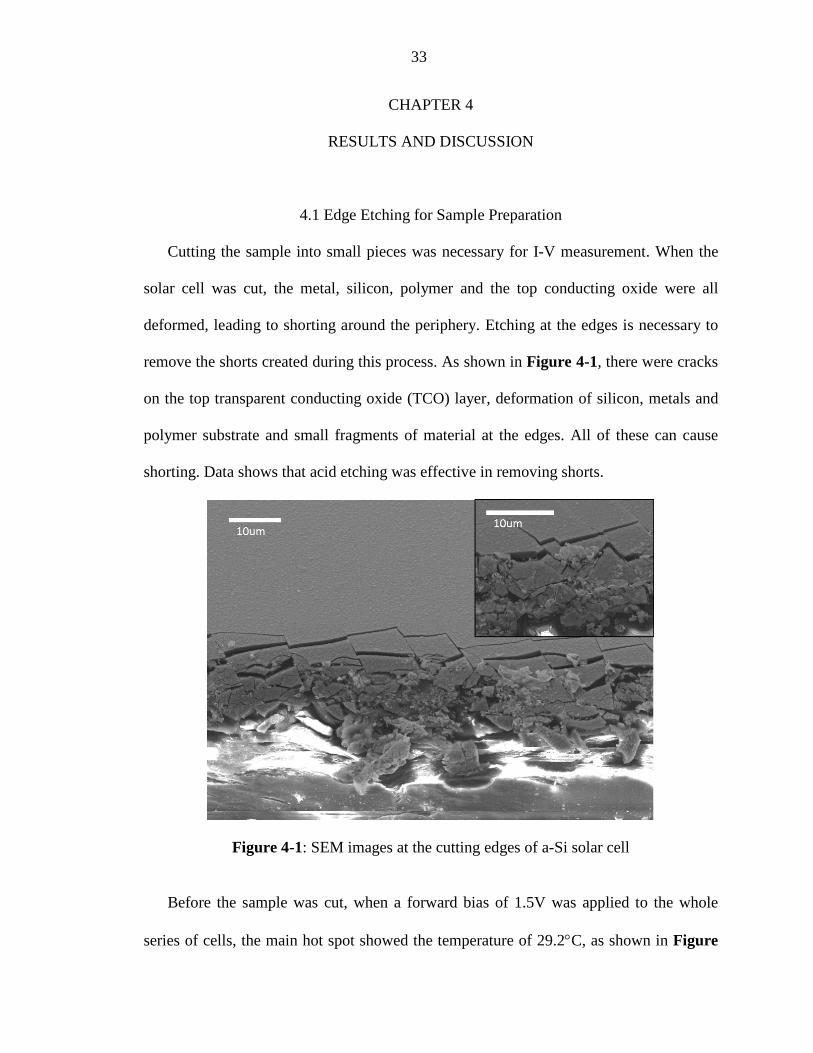
remove the shorts created during this process. As shown in Figure 4-1, there were cracks
on the top transparent conducting oxide (TCO) layer, deformation of silicon, metals and
polymer substrate and small fragments of material at the edges. All of these can cause
shorting. Data shows that acid etching was effective in removing shorts.
Figure 4-1: SEM images at the cutting edges of a-Si solar cell
Before the sample was cut, when a forward bias of 1.5V was applied to the whole
series of cells, the main hot spot showed the temperature of 29.2°C, as shown in Figure
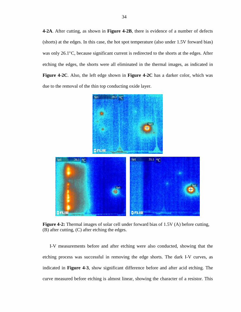
34
4-2A. After cutting, as shown in Figure 4-2B, there is evidence of a number of defects
(shorts) at the edges. In this case, the hot spot temperature (also under 1.5V forward bias)
was only 26.1°C, because significant current is redirected to the shorts at the edges. After
etching the edges, the shorts were all eliminated in the thermal images, as indicated in
Figure 4-2C. Also, the left edge shown in Figure 4-2C has a darker color, which was
due to the removal of the thin top conducting oxide layer.
Figure 4-2: Thermal images of solar cell under forward bias of 1.5V (A) before cutting, (B) after cutting, (C) after etching the edges.
I-V measurements before and after etching were also conducted, showing that the
etching process was successful in removing the edge shorts. The dark I-V curves, as
indicated in Figure 4-3, show significant difference before and after acid etching. The
curve measured before etching is almost linear, showing the character of a resistor. This
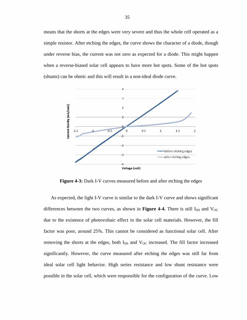
35
means that the shorts at the edges were very severe and thus the whole cell operated as a
simple resistor. After etching the edges, the curve shows the character of a diode, though
under reverse bias, the current was not zero as expected for a diode. This might happen
when a reverse-biased solar cell appears to have more hot spots. Some of the hot spots
(shunts) can be ohmic and this will result in a non-ideal diode curve.
Figure 4-3: Dark I-V curves measured before and after etching the edges
As expected, the light I-V curve is similar to the dark I-V curve and shows significant
differences between the two curves, as shown in Figure 4-4. There is still ISH and VOC
due to the existence of photovoltaic effect in the solar cell materials. However, the fill
factor was poor, around 25%. This cannot be considered as functional solar cell. After
removing the shorts at the edges, both ISH and VOC increased. The fill factor increased
significantly. However, the curve measured after etching the edges was still far from
ideal solar cell light behavior. High series resistance and low shunt resistance were
possible in the solar cell, which were responsible for the configuration of the curve. Low

36
shunt resistance was certainly caused by the existence of the main shunt in the solar cell.
High series resistance could indicate defects in the solar cell.
Figure 4-4: Illuminated I-V curves measured before etching the edges and after the edges
Through the light and dark I-V curves and the thermal images, it can be concluded
that the acid etching at the cutting edge can successfully remove the shorts caused by
cutting. Samples prepared in this way are ready for further characterization.
4.2 Thermal Imaging
The FLIR IR camera was used to detect hot spots under bias. The thermal images
were used to locate the hot spot and compare the performance of cells containing hot
spots and examine the effectiveness of removing damage through etching. Figure 4-5
shows thermal images of hot spots in solar cells under forward bias. For better resolution,
the scaling for the temperature was set to scale automatically. Spot 1 (Sp1) and spot 2
(Sp2) were two evident hot spots (Figure 4-5C and Figure 4-5D) and spot 3 (Sp3) was a
randomly chosen nearby spot.

37
Figure 4-5: Thermal imaging of solar cell hot spots under a forward bias of (A) 0V; (B) 1.2V; (C) 1.6V; (D) 2.0V
Figure 4-5A showed thermal image of a solar cell with 0 volt forward bias, showing
no hot spots. Due to the difference in emissivity, the silver fingers appear to be hotter
than the silicon, despite being at the same actual temperature.
Figure 4-5B, 4-5C and 4-5D showed thermal images of the same sample at the same
position with a forward bias of 1.2V, 1.60V and 2.0V respectively. With the increase of
voltage, the temperature of hot spot increased. Figure 4-6A shows that temperature of all
three spots increased with voltage. However, the I-V character of the solar cell, which is
shown in Figure 4-6B, indicates that there is low current when the voltage is below 1.4V,
resulting in less heating. When the voltage is higher than 1.4 where the current increases,
the temperature of these three spots was observed to increase. These two hot spots were
considered minor hot spots since they were less than 2 °C hotter than the rest of cell at
A B
C D

38
working voltage range (1.0V-1.8V). Note that spot 3 also increased in temperature
although there appears no discernable hot spot.
Figure 4-6: (A) Hot spots temperature increase with voltage, (B) I-V character when applied to a forward bias.
Different defects can result in hot spots of different intensity as demonstrated by the
two samples shown in Figure 4-7.These two samples have comparatively stronger hot
spots under forward bias, shown in Figure 4-7. Spot 1 is a clear hot spots and spot 2 was
randomly chosen spot on solar cell. Thermal imaging shows that in Figure 4-7A the hot
spot, which was under a forward bias of 1.6V, was 4.6 degrees hotter than the whole cell.
A
B

39
And in Figure 4-7B the hot spot was also under1.6V forward bias and was 8.6 degrees
hotter than the whole cell.
Figure 4-7: Two samples with primary hot spots under forward bias of 1.6V. (A) Cell one; (B) Cell two.
When the voltage was increased, the spot hot temperature also increased. In these two
samples, however, spot 2 did not change with increasing voltage. This is in contrast to the
sample in Figure 4-6A. Figure 4-8 shows temperature vs bias voltage curves of cell one
and cell two. It is clearly shown that the hot spot temperature increased significantly
while the reminder of the cell (as indicated by spot 2) is at constant temperature.
Comparing these with Figure 4-6, it can be inferred that minor hot spots do not redirect
significant current. The steady temperature increase with voltage in the sample with
minor hot spots appears uniformly all over the cell, not just the hot spots. However, the
existence of primary hot spots (shunts) can distribute the current such that little current
flows in the remaining portion of the cell as indicated by the stable temperature. In effect,
the majority of the current in the solar cell flows through shunts.
A B

40
Figure 4-8: Plot of temperature vs voltage
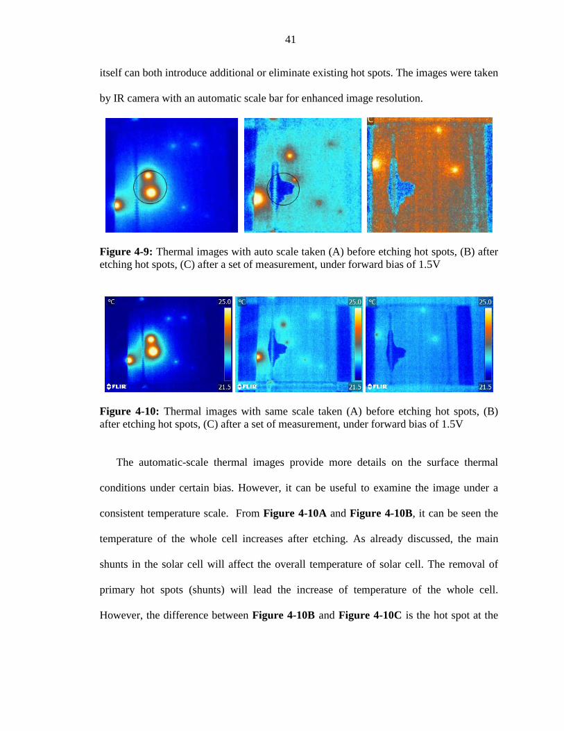
4.3 Effects of Hot Spot Etching
After etching the edges, the hot spots were also inspected with the IR camera and
selected hot spots were removed by acid etching, through a process specified earlier. In
Figure 4-9, there are some thermal images showing location and removal of hot spots
that show that while etching is effective in removing hot spots, the measurement process
Cell One
Cell Two
41
itself can both introduce additional or eliminate existing hot spots. The images were taken
by IR camera with an automatic scale bar for enhanced image resolution.
Figure 4-9: Thermal images with auto scale taken (A) before etching hot spots, (B) after etching hot spots, (C) after a set of measurement, under forward bias of 1.5V
Figure 4-10: Thermal images with same scale taken (A) before etching hot spots, (B) after etching hot spots, (C) after a set of measurement, under forward bias of 1.5V
The automatic-scale thermal images provide more details on the surface thermal
conditions under certain bias. However, it can be useful to examine the image under a
consistent temperature scale. From Figure 4-10A and Figure 4-10B, it can be seen the
temperature of the whole cell increases after etching. As already discussed, the main
shunts in the solar cell will affect the overall temperature of solar cell. The removal of
primary hot spots (shunts) will lead the increase of temperature of the whole cell.
However, the difference between Figure 4-10B and Figure 4-10C is the hot spot at the
42
left edges. This hot spot existed in Figure 4-10A and Figure 4-10B, but was eliminated
in Figure 4-10C. There are two possible causes:
1. The hot spot was caused by incomplete etching or improper handling, and thus the
hot spot was a weak short and was broken while handling during the
measurement;
2. The hot spot was burned out when reverse bias was applied to the sample.
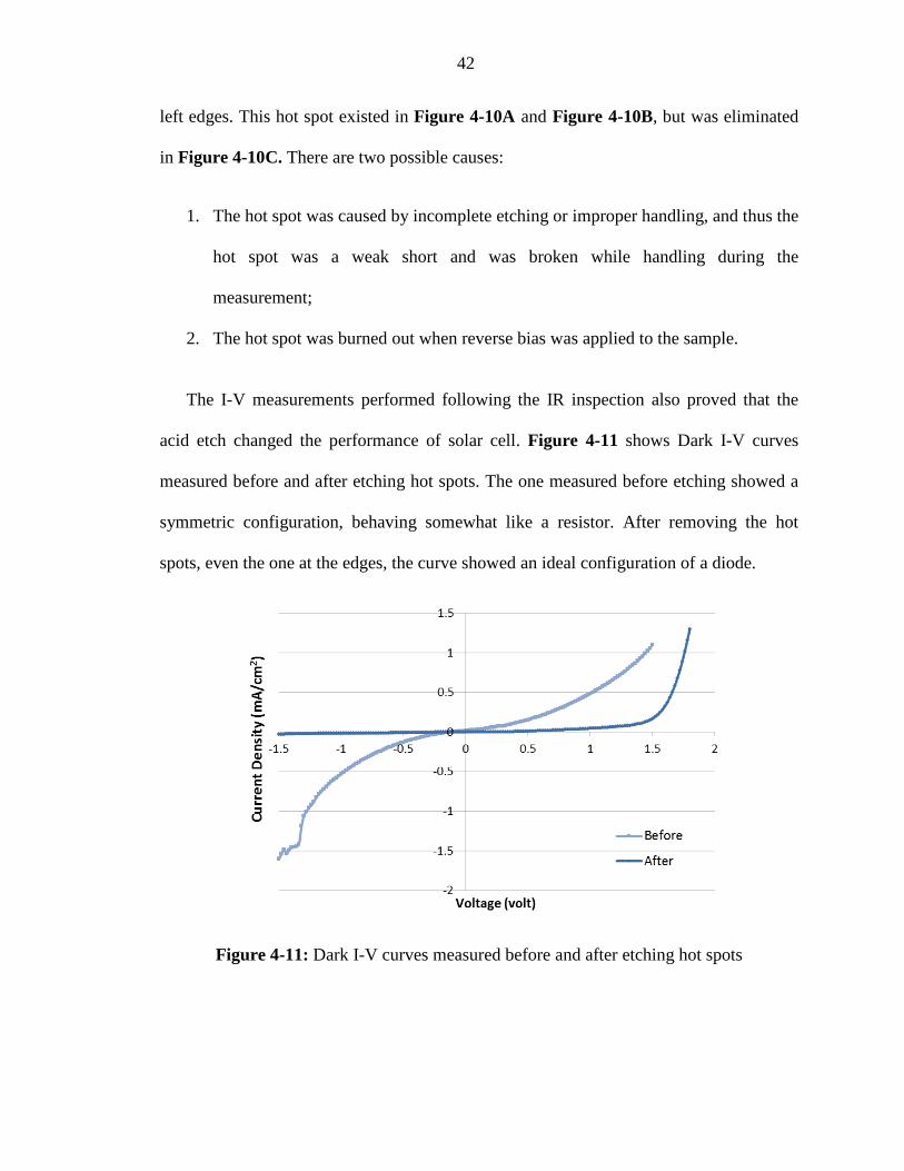
The I-V measurements performed following the IR inspection also proved that the
acid etch changed the performance of solar cell. Figure 4-11 shows Dark I-V curves
measured before and after etching hot spots. The one measured before etching showed a
symmetric configuration, behaving somewhat like a resistor. After removing the hot
spots, even the one at the edges, the curve showed an ideal configuration of a diode.
Figure 4-11: Dark I-V curves measured before and after etching hot spots
43
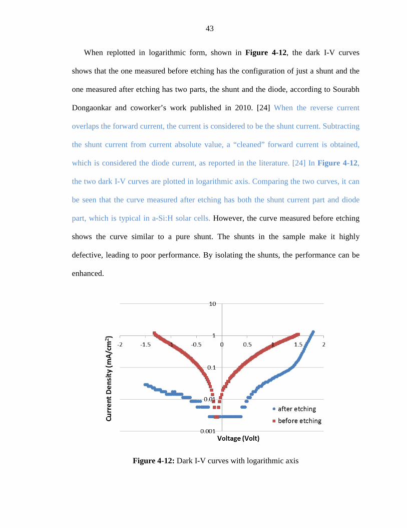
When replotted in logarithmic form, shown in Figure 4-12, the dark I-V curves
shows that the one measured before etching has the configuration of just a shunt and the
one measured after etching has two parts, the shunt and the diode, according to Sourabh
Dongaonkar and coworker’s work published in 2010. [24] When the reverse current
overlaps the forward current, the current is considered to be the shunt current. Subtracting
the shunt current from current absolute value, a “cleaned” forward current is obtained,
which is considered the diode current, as reported in the literature. [24] In Figure 4-12,
the two dark I-V curves are plotted in logarithmic axis. Comparing the two curves, it can
be seen that the curve measured after etching has both the shunt current part and diode
part, which is typical in a-Si:H solar cells. However, the curve measured before etching
shows the curve similar to a pure shunt. The shunts in the sample make it highly
defective, leading to poor performance. By isolating the shunts, the performance can be
enhanced.
Figure 4-12: Dark I-V curves with logarithmic axis

44
Light I-V curves were also measured following IR inspection. As is shown in Figure
4-13, the short circuit current didn’t change, but the open circuit voltage and fill factor
changed significantly.
Figure 4-13: Light I-V curves measured before and after etching hot spots
From Table 4-1, it can be conclude that under the light source the open circuit
voltage was improved by 20% from 1.31V to 1.57V; the fill factor was improved by
67.2% from 34.8 to 58.2; and maximum power was improved by 97.4% from 2.35mW to
4.64mW. At a specific light intensity, it can be noted that the efficiency also increased by
97.4%. The curve measured after etching showed an expected behavior for a normal solar
cell light I-V curve with low series resistance and low shunt resistance as measured from
the curve. This is consistent with the conclusion drawn from dark I-V analysis.
45
Table 4-1: Solar cell performance has been improved after etching the hot spot Before After Improvement
Isc 1.4 mA/cm2 1.41 mA/cm2 0 Voc 1.31V 1.57V 20% FF 34.8 58.2 67.2%
Max Power 2.35mW 4.64mW 97.4%
To investigate the extent to which the shunts affect the performance, several samples
were measured and compared. Data showed that removing the hot spots through etching
could drastically increase the VOC, FF, maximum power and thus efficiency. In the most
samples shown in Figure 4-14A, the ISC changed little or remain constant. In solar cells,
changes in shunt resistance affect voltage more than current. Thus, Figure 4-14B shows
that voltage increases for all samples. Samples with smaller voltages showed a large
increase. As previously reported, the parameter most drastically affected by etching is the
fill factor, which directly reflects the output power and conversion efficiency. The FF
chart below shows that FFs of all the samples before etching are around 30. The existence
of primary shunts leads to overall poor performance. After removing some of the main
spots, the fill factors all increased to some extent. While the absolute value of fill factors
measured do not indicate a good solar cell, it should be noted that the measurement
methods here are for comparison purposes only and should not be compared to
standardized measurements using a solar simulator. For comparison, FF can be increased
by 19%-67% by removing the main shunts. Together with all the other parameters,
maximum power is the most crucial in determining the performance of a solar cell. The
last chart in Figure 4-14 shows that maximum power increased significantly. The output
power or efficiency almost doubles. These numbers confirm that primary shunts in solar

46
cells severely affect the VOC, FF and efficiency and the acid etch method can reduce such
negative effects.
Figure 4-14: Comparison of electrical measurement data from before etching to after etching, which were obtained from four different samples. (A) shows the ISC changes; (B) (C) (D) shows the improvements by percentage of VOC, FF and Max power, respectively.
4.4 Examining The Degradation of Performance After Etching
The acid etch method of removing defects has the potential to degrade device
performance due to the corrosion of materials. In order to further characterize this
approach, a set of comparison experiments was conducted.
Dark and light I-V were measured immediately after the sample was first prepared
and hot spots were etched. The sample was then stored in a dry and dark environment for
three weeks and then I-V curves were remeasured using the same measurement
A B
D C

47
conditions (the same light intensity and same position of the sample). Figure 4-15 shows
light I-V curves before storing and after aging. The two curves are very similar within
experimental accuracy. The curves show no significant changes on VOC, ISH and FF.
Thus, efficiency is consistent.
Figure 4-15: Light I-V curve measured before and after a gap of three weeks
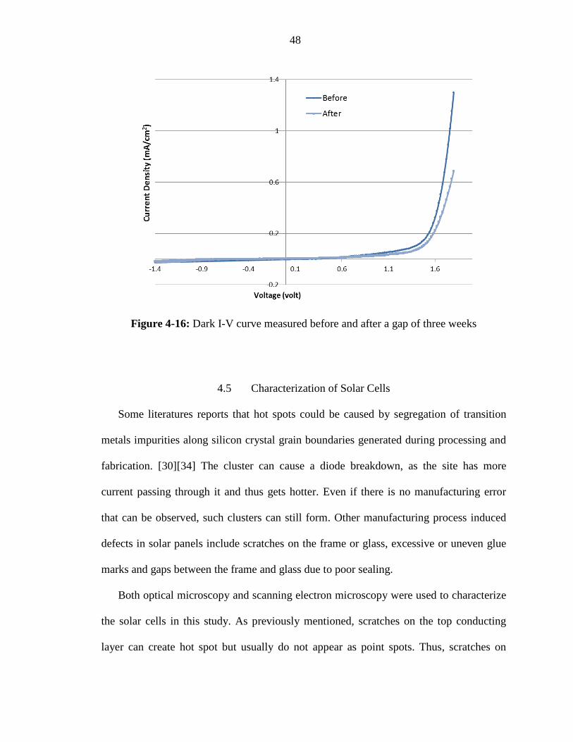
Light I-V curves were also measured and compared. There are still no significant
changes in the curvature but the current density has changed a small amount, as shown in
Figure 4-16. Since the current density is small, this variation may be within measurement
error.
According to the result from light I-V curves and dark I-V curves, the acid-etch
method has little influence on degradation on solar cell materials and performance within
the time frame measured.
48
Figure 4-16: Dark I-V curve measured before and after a gap of three weeks
4.5 Characterization of Solar Cells
Some literatures reports that hot spots could be caused by segregation of transition
metals impurities along silicon crystal grain boundaries generated during processing and
fabrication. [30][34] The cluster can cause a diode breakdown, as the site has more
current passing through it and thus gets hotter. Even if there is no manufacturing error
that can be observed, such clusters can still form. Other manufacturing process induced
defects in solar panels include scratches on the frame or glass, excessive or uneven glue
marks and gaps between the frame and glass due to poor sealing.
Both optical microscopy and scanning electron microscopy were used to characterize
the solar cells in this study. As previously mentioned, scratches on the top conducting
layer can create hot spot but usually do not appear as point spots. Thus, scratches on

49
transparent conducting oxide (TCO) are not considered as the likely cause for hot spots
imaged here. According to the work O. Breitenstein and coworker published in 2004,
[23] one of the causes for shunts are cracks and holes in the silicon layer. If there were
holes and cracks before final metallization or final coating process of TCO, the TCO or
other conductor will penetrate the silicon layer and lead to severe ohmic shunts. Thus, it
could be determined with careful microscopy whether such holes and cracks are the
primary cause of hot spots.
To determine whether such defects are visible with microscopy, a sample was cut and
inspected with SEM. Figure 4-17 shows that the TCO is thin compared to the amorphous
silicon layers. There were some cracks and small holes on the surface. However, these
cracks may have been caused by mechanical damage during handling and preparation.
Fig 4-17: SEM images of a-Si solar cells surface
To image the surface of the silicon layer, TCO must be removed and this was
accomplished with acid etching. As is shown in Figure 4-18, the optical microscope
image after etching the TCO indicated there were no significant visible flaws found on
the surface. However, a defect that results in a hot spot could be much smaller than what
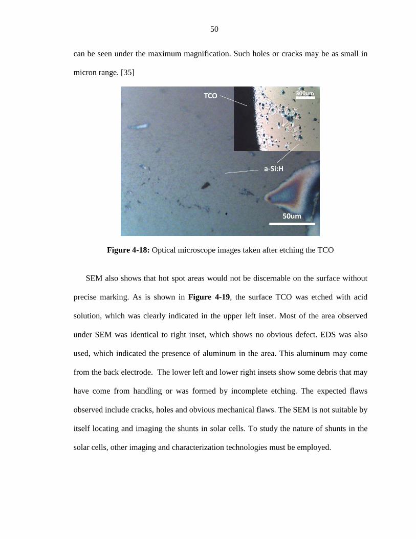
50
can be seen under the maximum magnification. Such holes or cracks may be as small in
micron range. [35]
Figure 4-18: Optical microscope images taken after etching the TCO
SEM also shows that hot spot areas would not be discernable on the surface without
precise marking. As is shown in Figure 4-19, the surface TCO was etched with acid
solution, which was clearly indicated in the upper left inset. Most of the area observed
under SEM was identical to right inset, which shows no obvious defect. EDS was also
used, which indicated the presence of aluminum in the area. This aluminum may come
from the back electrode. The lower left and lower right insets show some debris that may
have come from handling or was formed by incomplete etching. The expected flaws
observed include cracks, holes and obvious mechanical flaws. The SEM is not suitable by
itself locating and imaging the shunts in solar cells. To study the nature of shunts in the
solar cells, other imaging and characterization technologies must be employed.

51
Figure 4-19: SEM images of hot spot area on a-Si solar cell surface with the ITO etched away

52
CHAPTER 5
FUTURE WORK
Better precision could be achieved by repeating the above study with a solar
simulator and larger number of samples, but it is unlikely that this could yield
information regarding the characteristics and causes of shunts in these solar panels.
Other techniques must be employed.
An emerging promising technique that could be employed to further this study is that
of laser-based photoluminescence imaging.
PL imaging is a versatile technique that can characterize solar cell materials and
device properties. Spatial resolved PL can provide more details of the hot spots inspected
under an IR camera. IR imaging is limited by thermal blurring and thus has low
resolution. The actual size of the defect causing a hot spot cannot be measured through
thermal imaging. Photoluminescence imaging of solar cells has been developed over
recent years, offering vastly superior speed and spatial resolution. Both excitation and
detection are conducted by optical signals, and thus PL imaging is contactless. This can
alleviate measurement errors caused by contact problem.
Additionally, due to the correlation between local the PL signal and the local voltage
in solar cells, series resistance can also be imaged by PL, which can also allow
quantitative assessment. Furthermore, if the setup is also equipped with a PL
spectrometer, chemical composition variation over the solar cell can also be mapped.
More information about the nature of the defects formed in solar cells can be obtained
from such mapping. PL imaging and later analysis can be done with the same instrument

53
without moving the sample, which avoids the challenges related to locating and marking
areas of interest required for SEM and IR study.

54
REFERENCES
[1] R. Williams (1960). Becquerel Photovoltaic Effect in Binary Compounds, The Journal of Chemical Physics 32 (5): 1505–1514. [2] E. Becquerel (1839). "Mémoire sur les effets électriques produits sous l'influence des rayons solaires". Comptes Rendus 9: 561–567. [3] SunPower Corp., SunPower Announces World-Record Solar Panel With a 20.4 Percent Total Area Efficiency. (October 26, 2009) Retrieved, May 27, 2014, from http://investors.sunpower.com/releasedetail.cfm?ReleaseID=417965 [4] NPD Solarbuzz, Multicrystalline Silicon Modules to Dominate Solar PV Industry in 2014, According to NPD Solarbuzz (Oct. 25, 2013) Retrieved, May 27, from http://www.solarbuzz.com/news/recent-findings/multicrystalline-silicon-modules-dominate-solar-pv-industry-2014 [5] I.M. Dharmadasa, advances in thin-film solar cells, Singapore: Panstanford Publishing, 2013, Print. [6] Mathias Aarre Maehlum, (March 15, 2014). Best Thin Film Solar Panels – Amorphous, Cadmium Telluride or CIGS? Retrieve from: http://energyinformative.org/best-thin-film-solar-panels-amorphous-cadmium-telluride-cigs/ [7] FirstSolar Inc., First Solar Series 3 Black™ Module, Retrieve from: http://www.firstsolar.com/en/solutions/commercial-industrial. [8] FirstSolar Inc. (March 19, 2014), First solar sets thin-film modules efficiency world record of 17.0 percent, Retrieve from: http://investor.firstsolar.com/releasedetail.cfm?ReleaseID=833971 [9] Brian O'Regan, Michael Grätzel, "A low-cost, high-efficiency solar cell based on dye-sensitized colloidal TiO2 films". Nature 353 (6346): 737–740. [10] Y. Chibal, A. Islam, Y. Watanabe, R. Komiya, N. Koide and L. Han, Dye-sensitized solar cells with conversion efficiency of 11.1%, Jpn. J. Appl. Phys. Vol. 45, 638-640 (2006) [11] I. Chung, B. Lee, J. He, R. P. H. Chang, M. G. Kanatzidis, All-solid-state dye-sensitized solar cells with high efficiency, Nature, 2012, 485, 486. [12] RC Chittick, JH Alexander, HF Sterling, The preparation and properties of amorphous silicon, Journal of the electrochemical society, 1969; 116: 77-81

55
[13] Spear WE, Lecomber PG. Electronic properties of substitutionnally doped amorphous Si and Ge, Philosophical Magazine 1976; 33: 935–949. [14] Karl W. Böer, Handbook of the physics of Thin-Film Solar Cells, Berlin: Springer, 2013, Print [15] Shah, A. V., Schade, H., Vanecek, M., etc., Thin film silicon solar cell technology, J. Prog. PhotoVoltaics 2004, 12 (2-3), 113–142. [16] Green MA. Thin-film solar cells: review of technologies and commercial status. ANZSES Solar 05 Conference, Dunedin, November, 2005. [17] Carlson DE, Wronski CR, Pankove JI. Properties of amorphous silicon and a-Si solar cell, RCA review 1977; 38(2): 211-225. [18] Catalano A, D’Aiello R, Dresner J, Faughnan B, Firester A, Kane J, Schade H, Smith ZE, Swart G, Triano A., attainment of 10% conversion efficiency in amorphous silicon solar cells. Proceedings of the 16th IEEE photovoltaic specialists conference, San Diego, 1982; 1421-1422 [19] Martin A. Green, Third generation photovoltaics: Advanced solar energy conversion, Berlin; New York : Springer, Print [20] Guha S, Yang J. Science and technology of amorphous silicon alloy photovoltaics. IEEE Transactions on Electron Devices, 1999; 46: 2080–2085. [21] Guha S, Yang J, Pawlikiewicz A, Glatfelter T, Ross R, Ovshinsky SR. Bandgap profiling for improving the efficiency of amorphous silicon alloy solar cells. Applied Physics Letters, 1989; 54: 2330–2332. [22] Dhass. A.D., Natarajan E., Lakshmi Ponnusamy, Influence of Shunt Resistance on the performance of solar photovoltaic cell, International Conference on Emerging Trends in Electrical Engineering and Energy Management, IEEE Conf, 2012, pp: 382-386 [23] O. Breitenstein et al, Shunt Types in Crystalline Silicon Solar Cells, Prog. Photovolt: Res. Appl. 2004; 12:529–538 [24] S. Dongaonkar, J. D. Servaites, G. M. Ford, S. Loser, J. Moore, R. M. Gelfand, H. Mohseni, H. W. Hillhouse, R. Agrawal, M. A. Ratner, T. J. Marks, M. S. Lundstrom and M. A. Alam, J. Appl. Phys., 2010, 108, 124509–124510 [25] A. Simo, S. Martinuzzi, Proc. 21st IEEE PVSC (Kissimee 1990), 800 [26] FLIR Systems Inc., Thermal imaging cameras: a fast and reliable tool for testing solar panels. Retrieved June, 2014 from http://www.flir.com/cs/emea/en/view/?id=41872

56
[27] P.K. Kuo, T. Ahmed, H. Jin, R.L. Thomas, Phase-Locked Image Acquisition In Thermography, SPIE, 1004 (1988) 41. [28] X.P.V. Maldague, Theory and Practice of Infrared Technology for Nondestructive Testing, Wiley, New York, 2001. [29] O. Breitenstein, J.P. Rakotoniana, M. Kaes, S. Seren, T. Pernau, G.Hahn, W. Warta, and J. Isenberg, Lock-in thermalgraphy- a universal tool for local analysis of solar cells, 20th European Photovoltaic Solar Energy Conference, 6-10 June 2005, Barcelona, Spain, PP: 590-593 [30] B. Sopori, Impurities and Defects in Photovoltaic Si Devices: A Review, 10th International Workshop on the Physics of Semiconductor Devices, Delhi, India, December 13, 1999. [31] Keogh W, Blakers AW. Natural Sunlight Calibration of Silicon Solar Cells. 17th European Photovoltaic Solar Energy Conference. 2001 [32] Emery K, Myers D, Rummel S. SOLAR SIMULATION - PROBLEMS AND SOLUTIONS. 20th IEEE PV Specialists Conference. 1988 :1087. [33] G. Acciani, O. Falcone and S. Vergura, Analysis of the thermal heating of poly-Si and a-Si photovoltaic cell by means of Fem, International Conference on Renewable Energies and Power Quality, Granada (Spain), March, 2010 [34] Isolde E. Reis, Stephan Riepe, Wolfgang Koch, et al., Effect of impurities on solar cell parameters in intentionally contaminated multicrystalline silicon, 24th European Photovoltaic Solar Energy Conference, 21-25 September 2009, Hamburg, Germany [35] J. Bauer, W. Kwapil, D. Lausch, M.C. Schubert, W. Warta, K. Bothe, O. Breitenstein, Comments on the paper “Detection and analysis of hot-spot formation in solar cells” published by M. Simon and E.L. Meyer in Solar Energy Materials & Solar Cells 94 (2010) 106–113, Solar Energy Materials and Solar Cells, 2012; 99:362–364 [36] T. R. Johnson, G. Ganguly, G. S. Wood, and D. E. Carlson, “Investigation of the causes and variation of leakage currents in amorphous silicon p-i-n diodes”, in Amorphous and Nanocrystalline Silicon-Based-Films-2003, Vol. 762, (Materials Research Society, Warrendale, PA, 2003), pp. 381–386.

57
ACKNOWLEDGEMENTS
I would like to express my sincere appreciation to my major professor Dr. Kristen
Constant, who has been continuously giving me guidance and inspiring me for course
study and project research. I would like to thank Dr. Kaiming Ho for proving me the
opportunity to work in the lab and for his strong and helpful supports to my research. I
would also like to thank Dr. Sumit Chaudhary, who has been offering me valuable
suggestions on my research.
I would like to thank my group member Geyuan Liu, from who I have learned a lot of
precious experience in the lab. I shall also thank other group members Dr. Joongmok
Park, Dr. Wai Leung and Yuqing Chen, who have offered me lots of assistance and
taught me technical skills for research and experiments.
Finally, I want to express my thankfulness to my parents, Xianqing Jiang and
Jianqiang Chen. Without their support and love, I cannot go this far and they will
continue to be my strongest support.