1
Dr. Jeff Jackson Lecture 4-1Electrical & Computer Engineering – Embedded Systems
Embedded Systems
The Altera NIOS II Embedded Development Kit Overview
Dr. Jeff Jackson Lecture 4-2Electrical & Computer Engineering – Embedded Systems
NIOS II Embedded Evaluation Kit Features
• Cyclone III EP3C25F324 FPGA– 25,000 logic elements (LEs)– NIOS II processor implemented on this device
• 32 MB DDR SDRAM• 1 MB synchronous SRAM• 16 MB Flash• 50MHz on-board oscillator (fundamental clock source)• Four user controlled pushbuttons, four user-controlled LEDs• LCD daughter card (High Speed Mezzanine Card – HSMC)
– 800x480 touch-screen LCD display– 24-bit CD-quality audio coder/decoder (CODEC)
• Can be used as basic ADC/DAC circuitry
– SD card socket– Ethernet 10/100 Mbps– VGA output– Composite video input– PS2 connector– RS-232 connector

2
Dr. Jeff Jackson Lecture 4-3Electrical & Computer Engineering – Embedded Systems
Block Diagram of NIOS II Embedded Evaluation Kit
Dr. Jeff Jackson Lecture 4-4Electrical & Computer Engineering – Embedded Systems
Cyclone III FPGA Starter Board

3
Dr. Jeff Jackson Lecture 4-5Electrical & Computer Engineering – Embedded Systems
Top View of the Cyclone III FPGA Starter Board
Dr. Jeff Jackson Lecture 4-6Electrical & Computer Engineering – Embedded Systems
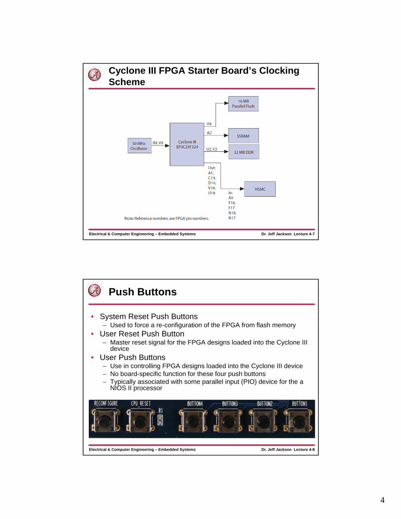
Clocking Circuitry
• A single 50 MHz clock input is used and all other clocks are generated using the Cyclone III device’s phase-locked loops (PLLs)
• The dedicated PLLs are used to distribute the flash, SSRAM, and HSMC clocks– All necessary clocks for all components– Some may be slower/faster than the NIOS II processor
core clock– The NIOS II clock itself is usually derived from the 50
MHz clock (using a PLL)• Various NIOS II systems may execute at different clock rates• Use care in creating code that depends on a specific processor
clock rate (e.g. software delay loops, etc.)
4
Dr. Jeff Jackson Lecture 4-7Electrical & Computer Engineering – Embedded Systems
Cyclone III FPGA Starter Board’s Clocking Scheme
Dr. Jeff Jackson Lecture 4-8Electrical & Computer Engineering – Embedded Systems
Push Buttons
• System Reset Push Buttons– Used to force a re-configuration of the FPGA from flash memory
• User Reset Push Button– Master reset signal for the FPGA designs loaded into the Cyclone III
device
• User Push Buttons– Use in controlling FPGA designs loaded into the Cyclone III device– No board-specific function for these four push buttons– Typically associated with some parallel input (PIO) device for the a
NIOS II processor
5
Dr. Jeff Jackson Lecture 4-9Electrical & Computer Engineering – Embedded Systems
LEDs
• User LEDs– Status and debugging signals are driven to the user LEDs from
FPGA designs loaded into the Cyclone III device– No board-specific function for these LEDs– Typically associated with some parallel output (PIO) device for
the a NIOS II processor
• Board Specific LEDs– Power indicator, configuration LED, etc.
Dr. Jeff Jackson Lecture 4-10Electrical & Computer Engineering – Embedded Systems
LCD Multimedia HSMC
• MAX II CPLD used for– Time-division multiplexing of signals– Voltage level shifting
• Interfaces– HSMC expansion interface– Audio codec interface– Video decoder interface– VGA interface– Serial interface– PS/2 interface– Ethernet
• Clocking circuitry• Memory

6
Dr. Jeff Jackson Lecture 4-11Electrical & Computer Engineering – Embedded Systems
Top View of the LCD Multimedia HSMC
Dr. Jeff Jackson Lecture 4-12Electrical & Computer Engineering – Embedded Systems
Interface Device
• The LCD Multimedia HSMC uses the MAX II 2210 CPLD device
• The primary functions for this device are to:– Provide time-division multiplexing (TDM) functions to the
LCD and VGA color data bus
– Provide level shifting feature for the 2.5V input (Cyclone III FPGA) and 3.3V required by many of the interface chips

7
Dr. Jeff Jackson Lecture 4-13Electrical & Computer Engineering – Embedded Systems
Block Diagram of MAX II Bus Controller