1
ABSTRACT
Title: ELECTROSTATIC DISCHARGE AND
ELECTRICAL OVERSTRESS FAILURES OF
NON-SILICON DEVICES
Yu-Chul Hwang
Doctor of Philosophy, 2004 Directed By: Professor Michael G. Pecht
Department of Mechanical Engineering Electrostatic discharge (ESD) causes a significant percentage of the failures in the
electronics industry. The shrinking size of semiconductor circuits, thinner gate oxides,
complex chips with multiple power supplies and mixed-signal blocks, larger chip
capacitance and faster circuit operation, all contribute to increased ESD sensitivity of
advanced semiconductor devices. Therefore, understanding and controlling ESD is
indispensable for higher quality and reliability of advanced device technologies.
This thesis provides a comprehensive understanding of ESD and EOS failures in
GaAs and SiGe devices. In the first part of this thesis, characteristics of internal damage
caused by several ESD test models and EOS stress in non-silicon devices (GaAs and
SiGe) are identified. Failure signatures are correlated with field failures using various
failure analysis techniques.
The second part of this thesis discusses the effects of ESD latent damage in GaAs
devices. Depending on the stress level, ESD voltage can causes latent failures if the
device is repeatedly stressed under low ESD voltage conditions, and can cause premature

2
damage leading eventually to catastrophic failures. Electrical degradation due to ESD-
induced latent damage in GaAs MESFETs after cumulative low-level ESD stress is
studied. Using failure analysis, combined with electrical characterization, the failure
modes and signatures of EOS stressed devices with and without prior low-level ESD
stress are compared.
To predict the power-to-failure level of GaAs and silicon devices, an ESD failure
model using a thermal RC network was developed. A correlation method of the real ESD
stress and square wave pulse has been developed. The equivalent duration of the square
pulse is calculated and proposed for the HBM ESD stress. The dependence of this value
on the ESD stress level and material properties is presented as well.
3
ELECTROSTATIC DISCHARGE AND ELECTRICAL
OVERSTRESS FAILURES OF NON-SILICON DEVICES
By
Yu-Chul Hwang
Dissertation submitted to the Faculty of the Graduate School of the University of Maryland at College Park in partial fulfillment
of the requirements for the degree of Doctor of Philosophy
May 2005
Advisory Committee:
Professor Michael Pecht, Advisor Professor Christopher Davis Associate Professor Peter Sandborn Associate Professor Patrick McCluskey Associate Professor Omar Ramahi

i
© Copyright by Yu-Chul Hwang
2005

ii
ACKNOWLEDGEMENTS
This dissertation is the result of three and half years of work through which I
have been accompanied and supported by many people around me. It is pleasant
that I have now the opportunity to express my gratitude to all of them.
First, I am greatly grateful to my advisor, Dr. Michael G. Pecht, for his
academic guidance and support throughout my Ph.D. studying, for his wisdom,
open mind, and illuminations when I need most, for his energetic working style that
gave me guidance to develop and complete my research and academic work.
Second, I would like to thank Dr. Christopher Davis, Dr. Patrick McCluskey,
Dr. Sandborn and Dr. Omar Ramahi for kindly consenting to be on my thesis
committee and their time, suggestions and comments. I also want to give my special
thanks to Dr. Mikyoung Lee who has kept an eye on the progress of my research,
who has been always available when I needed her advises. I would like to thank Dr.
BongTae Han for his kind advice on my research, course work, serving as a Ph. D.
qualifying exam committee and life in the U.S. for last three and half years. His
strict and extensive comments and instructions had a direct impact on the quality of
Ph. D. work and improvement of my research and presentation skills as well.
I am grateful to my many Korean friends in CALCE, Chang-Woon, Junpyo,
Seungmin, Seunyeol, Yuri, Kyoungjun, and Dae-Whan.
Mr. Ho-Sung Jeon, Dong-Su Ryu, and Jin-Woo Kim for introducing me to
the CALCE Center and their advices and help over the years in my six year working
period at the Quality and Reliability Lab. of Daewoo Electronics Co. Ltd.. I am also
iii
grateful to Dr. Das for his instructions that helped me get started in the new
environment, Keith Rogers for his friendship, his unselfish help in the laboratory as
well as his encouragement, Ping Zhao who started Ph. D. work at the same time
with me, Tong Fang, Sanjay Tiku, Yuki Fukuda, Sheng Zhen and other teammates
who made the office a pleasant place for work and study, Dr. Azarian and Mr. Chris
Wilkinson, for discussions during the last period of my thesis.
I would like to give thank to many of my friends in Korea (Bon-Young,
Seoung-Hoon, Inseon, Heon-Gyu, Jae-Woo, Inchan, Si-Young, Sea-Jong, Hyun-
Jung, Dong-Ju, Jae-Sang, Hyuk-Jae, Jin-Young, Hack-Soo, Jae-Goo, Min-Gyu,
Hac-Ju, Chan-Hee, Dong-Kyung and many others). Even though we have not seen
each other for a long time, our continuous communications over the phone and on
the web have always reminded me of lovely memories of my homeland, Korea.
I would like to express heartfelt thanks to all colleagues and other people in
the CALCE Electronic Products and Systems Center, Department of Mechanical
Engineering, for their valuable help and friendship.
Last but certainly not least, I am especially indebted to my wife, Dami, my
lovely daughter Emily, and parents in Korea for their encouragement, support, and
love, as always.

iv
TABLE OF CONTENTS
TABLE OF CONTENTS ......................................................................................... IV
LIST OF TABLES.................................................................................................... VI
LIST OF FIGURES.................................................................................................VII
LIST OF FIGURES.................................................................................................VII
1. INTRODUCTION .............................................................................................. 1
1.1 Creating Electrostatic Charge..................................................................... 3
1.2 ESD/EOS Effects in Electronic Industries ................................................. 6
1.3 ESD/EOS Protection Circuits ................................................................... 10
2. ESD CHARACTERIZATION IN IC DEVICES............................................. 14
2.1 Basic Device Physics................................................................................ 15
2.2 ESD/EOS Induced-Failure Mode and Mechanism................................... 17
2.3 ESD Test Models...................................................................................... 21
3. OBJECTIVES AND OUTLINE OF THIS THESIS ........................................ 33
4. FAILURE ANALYSIS AND ESD EVALUATION OF SIGE OPAMPS...... 36
4.1 SiGe devices and ESD.............................................................................. 36
4.2 Wideband Fixed-Gain Amplifiers ............................................................ 40
4.3 ESD test and electrical characterization ................................................... 42
4.4 Failure analysis results.............................................................................. 47
4.5 Discussions and conclusions .................................................................... 54
5. INVESTIGATION OF FIELD FAILURES AND FAILURES CAUSED BY
EOS AND ESD IN GAAS MMIC ........................................................................... 59
5.1 GaAs devices and ESD............................................................................. 59
5.2 Experimental approach............................................................................. 61
5.3 ESD and EOS failure threshold test results .............................................. 64
5.4 Failure analysis results.............................................................................. 65
5.4.1. Failure mode identifications ............................................................. 66
5.4.2. X-Ray observation............................................................................ 67
5.4.3. Decapsulation and optical microscopy/ESEM observations ............ 68
5.5 Summary and conclusions ........................................................................ 72

v
6. ESD-INDUCED LATENT FAILURES........................................................... 76
6.1 ESD Latent failure .................................................................................... 76
6.2 GaAs Devices and Latent Failure............................................................. 78
6.3 Experimental procedure............................................................................ 79
6.4 Test Results............................................................................................... 82
6.4.1. ESD/EOS failure threshold test results............................................. 82
6.4.2. ESD latent damage test result ........................................................... 83
6.4.3. EOS test after low level ESD stress.................................................. 85
6.4.4. The effect of thermal annealing........................................................ 87
6.5 Failure Analysis Results ........................................................................... 88
6.5.1. ESD stressed device.......................................................................... 88
6.5.2. EOS stressed devices with no prior ESD stress................................ 89
6.5.3. EOS stressed devices with initial ESD stress ................................... 90
6.5.4. Field failed devices ........................................................................... 93
6.6 Conclusions .............................................................................................. 93
7. ESD FAILURE PREDICTION ........................................................................ 95
7.1 Background of ESD Failure Prediction and Power-to-Failure Prediction
Models .................................................................................................................. 95
7.2 Heat Flow Model Using Thermal RC Circuit .......................................... 99
7.3 Power-to-failure generation.................................................................... 103
7.4 Failure prediction for ESD pulse ............................................................ 106
7.5 Correlation of ESD and square pulse ..................................................... 109
7.6 Conclusions ............................................................................................ 112
8. CONTRIBUTIONS........................................................................................ 114
9. REFERENCES............................................................................................... 116
vi
LIST OF TABLES
Table 1.1 Possible ESD phenomena in real life [6].................................................... 4
Table 1.2 Loses due to ESD in electronic industries [12] .......................................... 7
Table 2.1 ESD immunity classification .................................................................... 31
Table 4.1 Properties of semiconductor materials [34]-[36]...................................... 37
Table 4.2 Features, applications, and device data .................................................... 41
Table 4.3 Absolute maximum ratings....................................................................... 41
Table 4.4 Recommended operating conditions ........................................................ 41
Table 4.5 ESD failure threshold test results ............................................................. 43
Table 4.6 Measurements of electrical parameters (DC characteristics) of all the 20
devices before being subjected to ESD stress .................................................. 46
Table 4.7 Electrical parameters (DC characteristics) measured after ESD exposure
.......................................................................................................................... 46
Table 4.8 Characteristics of failure signatures ......................................................... 54
Table 5.1 ESD and EOS failure threshold test results .............................................. 64
Table 5.2 Devices investigated for failure analysis .................................................. 65
Table 5.3 Characteristics of failure signatures ......................................................... 73
Table 6.1 ESD and EOS failure threshold test result ............................................... 82
Table 6.2 ESD/EOS threshold test results after multiple stresses ............................ 86

vii
LIST OF FIGURES
Figure 1.1 The mechanism of triboelectric charge – contact and separation [3]........ 3
Figure 1.2 Distribution of failure causes in IC devices [9], [10]................................ 6
Figure 1.3 Pareto chart of the failure causes of IC devices [11]................................ 7
Figure 1.4 Fishbone Diagram for Electrostatic discharge failures on IC devices [13]
............................................................................................................................ 9
Figure 1.5 Typical CMOS input protection scheme................................................. 11
Figure 2.1 Decrease in thermal conductivity of silicon with increasing temperature
[25].................................................................................................................... 16
Figure 2.2 A rapid decrease in resistivity of doped silicon with increasing
temperature [25] ............................................................................................... 16
Figure 2.3 Cross sectional drawing of ESD damage in bipolar structures [25] ....... 20
Figure 2.4 Cross sectional drawing of ESD damage in MOS structures [25] .......... 20
Figure 2.5 HBM ESD waveform at 500 V, short circuit [26] .................................. 22
Figure 2.6 HBM test circuit [26] .............................................................................. 22
Figure 2.7 Machine model waveform at 500 V, short circuit [26] ........................... 25
Figure 2.8 MM ESD test circuit [28]........................................................................ 25
Figure 2.9 CDM ESD test setup ............................................................................... 27
Figure 2.10 Typical current waveform from CDM .................................................. 27
Figure 4.1 Advantages of SiGe devices.................................................................... 38
Figure 4.2 Pin assignments and top view) ................................................................ 40
Figure 4.3 Test setup used for DC characteristics measurements ............................ 44
Figure 4.4 Typical DC characteristics with Vs=±2.5V before and after ESD stress 45
Figure 4.5 Failure analysis procedure....................................................................... 47
Figure 4.6 Test set-up for liquid crystal thermal imaging analysis .......................... 49
Figure 4.7 Liquid crystal analysis result for a good device...................................... 49
Figure 4.8 Liquid crystal analysis result for failed devices ...................................... 50
Figure 4.9 HBM ESD testing showing transient failure on ESD protection circuitry
.......................................................................................................................... 51

viii
Figure 4.10 MM ESD testing showing transient failure on ESD protection circuitry
.......................................................................................................................... 52
Figure 4.11 CDM ESD testing showing transient failure on ESD protection and
internal circuitry of the gain stage .................................................................... 53
Figure 4.12 ESD paths through the internal circuit .................................................. 56
Figure 5.1 Flowchart of failure analysis process ...................................................... 61
Figure 5.2 Schematic circuit of the device ............................................................... 62
Figure 5.3 Failure mode identifications.................................................................... 66
Figure 5.4 X-Ray observations (top vie and side view) ........................................... 67
Figure 5.5 HBM-stressed device .............................................................................. 68
Figure 5.6 HBM-stressed device .............................................................................. 69
Figure 5.7 MM-stressed device ................................................................................ 69
Figure 5.8 CDM-stressed device .............................................................................. 70
Figure 5.9 EOS stressed device ................................................................................ 70
Figure 5.10 Field failed device ................................................................................. 71
Figure 5.11 Field failed device showing the failure in the resistor area and a
mechanical crack in the capacitor area............................................................. 71
Figure 6.1 Experimental procedure .......................................................................... 79
Figure 6.2 Leakage current comparison (IGDO) ........................................................ 84
Figure 6.3 Drain-source current (IDS, VGS=1V)........................................................ 85
Figure 6.4 EOS failure threshold comparison .......................................................... 87
Figure 6.5 ESD stressed device ................................................................................ 89
Figure 6.6 EOS-stressed device (with initial 80 %of ESD failure threshold voltage)
.......................................................................................................................... 90
Figure 6.7 EOS-stressed device (with initial 80 %of ESD failure threshold voltage)
.......................................................................................................................... 91
Figure 6.8 EOS-stressed device (with initial 20 %of ESD failure threshold voltage)
.......................................................................................................................... 91
Figure 6.9 EOS-stressed device (with initial 50 %of ESD failure threshold voltage)
.......................................................................................................................... 92

ix
Figure 7.1 (a) 3D thermal box region of heat dissipation for power-to-failure
prediction in an NMOS transistor, (b) Schematic of power-to-failure vs. width
of a square wave pulse...................................................................................... 98
Figure 7.2 Electrical-thermal equivalent schematic of a solid ................................. 99
Figure 7.3 Cross-sectional structure and heat source region .................................. 100
Figure 7.4 Electrical-thermal analogy modeling for heat source region ................ 101
Figure 7.5 Power-to-failure and Time-to-Failure (Tf) Determination .................... 104
Figure 7.6 Power-to-failure versus pulse duration, measurement versus prediction
for a silicon device.......................................................................................... 104
Figure 7.7 Comparison of predicted power-to-failure of silicon and GaAs devices
........................................................................................................................ 105
Figure 7.8 HBM current waveform for failure prediction...................................... 106
Figure 7.9 Temperature rise profile from the HBM ESD pulses............................ 107
Figure 7.10 Current profile and temperature rise from HBM ESD pulse .............. 109
Figure 7.11 Temperature rise from HBM ESD and square pulse .......................... 110
Figure 7.12 Correlation result for HBM ESD pulse and square pulse ................... 111

1
1. INTRODUCTION
Electrostatic discharge (ESD) is one of the most important reliability
problems in the integrated circuit industry. Typically, it is known that one-third to
one-half of all field failures are due to ESD and other failures known as electrical
overstress (EOS) [1], [2]. Therefore, to achieve higher quality and reliability
standards for IC products and to reduce the IC product loss due to ESD and EOS
related failures, ESD phenomenon should be well understood and controlled and
proper corrective actions should be taken through all phases of IC device design,
manufacturing, and use. As ESD damage has become more prevalent in newer
technologies due to the higher susceptibility of smaller circuit components, there has
been a corresponding increase in efforts to understand ESD failures through
modeling and failure analysis. This has resulted in a greater industry-wide
knowledge of ESD mechanisms and thus a greater ability to design robust ICs
which sustain fewer field failures and in order to obtain higher ESD robustness of
IC devices, significant progress has been made in understanding the implications of
different types of ESD events on the design of protection circuits, and in
implementing highly effective ESD protection circuits at each device technology.
However, despite these efforts, there are still ESD-related problems which
are not well understood. The advent of new generation of device technology always
leads to new challenges to higher ESD reliability and more efficient protection
circuit. ESD is comparatively well known issues in silicon devices and seriously
addressed during past years from the many researchers, but the ESD issue in non-

2
silicon devices such as GaAs and SiGe devices is only discussed in very few
publications. Although significant progress has been made in understanding ESD
and solving ESD related problems, there is still much room for improvement in the
case of non-silicon devices.
Electronic system manufacturers and microelectronics device manufacturers
claimed that they have trouble with microelectronics devices damaged after system
level burn-in screening. Although the companies comprehended the possibility that
the failure has occurred due to EOS or ESD, they have had difficulty in identifying
failure causes and the process conditions that lead for damage. However, they need
to define failure causes before the right protection can be implemented.
There have been efforts to find evidence of ESD and EOS failures in various
process technologies for the last twenty years. But not nearly enough work has been
done on classifying various ESD and EOS conditions such as the combination of
ESD modes or continuous EOS in accordance with failure characteristics.
Classification of failure characteristics will lead to a description of the quantitative
causes of failure and this is an important process because manufacturers can
understand why, where, and when these failures occur.
The focus of this thesis is on the characterization of ESD/EOS related IC
failures, particularly for non-silicon devices using GaAs and SiGe. The objective of
this study is to clarify ESD/EOS events experimentally and theoretically, and their
effects on semiconductor devices due to the high voltage and current. In order to
study ESD/EOS phenomenon, extensive experiments have been conducted, and an
analytical model for failure of IC devices is described to explain failure

3
mechanisms. An outline of the thesis and a list of its objectives are presented in
chapter 3.
1.1 Creating Electrostatic Charge
ESD is a subset of electrical overstress (EOS) and can be defined as “the
transfer of charge between two bodies at different electrical potentials” [3] either
through direct contact or through an induced electric field, so it is a charge driven
physical mechanism resulting from a charge imbalance. There are three major
charge-generation processes; triboelectric charging, induction, and conduction [4].
But usually, this imbalance of electrons on the surface of the material is caused by
friction between different materials, which is called triboelectric charging. The
potential induced by charges depends on the triboelectric properties of materials,
contact area, pressure applied, and friction between the two materials [5]. For
example, a person walking across the floor generates static electricity as shoe soles
+ ++
--
-
--
-
Material A Material B
(a) Material contact
-
-
--
-
Material A Material B
(b) Material separation
-+ +
++ +
++ +
++ +
+
--
-
--
-
Material A Material B
(a) Material contact
-
-
--
-
Material A Material B
(b) Material separation
-+ +
++ +
++ +
+
Figure 1.1 The mechanism of triboelectric charge – contact and separation [3]

4
Table 1.1 Possible ESD phenomena in real life [6]
contact and then separate from the floor surface. An electronic device sliding into or
out of a bag, magazine or tube generates an electrostatic charge as the device's
housing and metal leads make multiple contacts and separations with the surface of
the container. While the magnitude of electrostatic charge may be different in these
examples, static electricity is indeed generated. Table 1.1 shows that huge
electrostatic voltage can be generated even during normal daily life.
Triboelectric charging is generated by a contact and separation mechanism.
In an electrically neutral condition, the atoms of materials have same number of
positive protons and negative electrons. As shown in Figure 1.1(a), material "A"
consists of atoms with equal numbers of protons and electrons. Material "B" also
consists of atoms with equal (though perhaps different) numbers of protons and
electrons. Once they are placed into contact and separated (Figure 1.1(b)), negatively
charged electrons are transferred from the surface of one material to the surface of
the other material. Which material loses electrons and which gains electrons is
1500V18000VChair packed with polyurethane foam
1200V20000VPolyethylene bag lifted from a bench
7000V 600VVinyl cover
250V1200VPerson walking on a vinyl floor1500V3500VPerson walking on a carpet
65 to 90% RH10 to 20% RHGenerating Source
Electrostatic voltageExamples of electrostatic voltage
1500V18000VChair packed with polyurethane foam
1200V20000VPolyethylene bag lifted from a bench
7000V 600VVinyl cover
250V1200VPerson walking on a vinyl floor1500V3500VPerson walking on a carpet
65 to 90% RH10 to 20% RHGenerating Source
Electrostatic voltageExamples of electrostatic voltage

5
totally dependent on the tribo-electrical properties of the two materials. In the
example of Figure 1.1, the material "A" that loses electrons is charged positively
and the material "B" that gains electrons is charged negatively.
This process of material contact, electron transfer and separation is really a
more complex mechanism than described here. The amount of charge created by
triboelectric generation is affected by the area of contact, the speed of separation,
relative humidity, and other factors. Once the charge is created on a material, it
becomes an electrostatic charge if it remains on the material. This charge may be
transferred from the material, creating an electrostatic discharge, or ESD, event.
Additional factors such as the resistance of the actual discharge circuit and the
contact resistance at the interface between contacting surfaces also affect the actual
charge that can cause damage. Even though triboelectric charging is the most
common static charge generation mechanism, it can be generated by induction and
conduction.
An electrostatic charge also may be created on a material in other ways such
as by induction and conduction. Inductive charging is a two-step process. As a
conductive object comes into close with a charged object, part of the field
terminates on a conductive object, resulting in an internal separation of charge.
When a charged object is removed from the area, a net charge exists on a conductive
object but opposite in polarity from what existed on a charged object. The transient
caused by induction is similar to a charged device model (CDM) event [7].
One more charging process, conductive charging involves the physical
contact and balancing of voltage between two systems or objects at different

6
potentials. As a charged object is brought into physical contact with an isolated
object of lower potential, charge is transferred to the lower biased object until the
potential is balanced. When the objects are separated, the two objects have
accumulated a charge of the same polarity.
1.2 ESD/EOS Effects in Electronic Industries
ESD may be able to change the electrical or physical properties of electronic
devices, including semiconductor devices, degrading or destroying them (will be
explained in Chapter 2). ESD combined with EOS is one of the most frequently
occurring failures in the IC device industry and the potentially destructive nature of
ESD in IC devices became more apparent as IC devices became smaller and more
complex. As shown in Figure 1.2 (a), it is known that around 60 % of total IC
failures are caused by ESD and ESD. A Pareto chart for both plastic and hermetic
IC devices also shows that the number one failure mechanism is ESD/EOS (Figure
1.3). So there is no wonder that ESD/EOS is one of the most important failure
(a) Distribution of failure causes in Silicon ICs
EOS & ESD
58% 27%
Design, process, assembly related
25%
17%ETC No problem
41%
Application
19%
ETC(Design, not found,untestable)
(b) Distribution of failure causes in GaAs ICs Figure 1.2 Distribution of failure causes in IC devices [9], [10]

7
mechanisms in IC devices. Furthermore this ESD/EOS issue is expected to remain
important for future IC technology and future IC device materials like GaAs and
SiGe devices [8], [10]. (Figure 1.2 (b)) and this is also applicable to different types
of device technologies such as CMOS, bipolar, and MESFETs. In both Figure 1.2
Table 1.2 Loses due to ESD in electronic industries [12]
Failure Causes
0
5
10
15
20
25
EOS & ESD
Unresol
ved
Gold Ball
Bond Fail
at Bail
Bond
Not Veri
fiedOthers
Gold Ball
Bond
Fail at
Stitch B
ond
Shear
Stress-C
hip su
rface
Corrosio
n-Chip
Metalliz
ation/A
ssembly
Dielect
ric Fail
, Poly
-Meta
l, Meta
l-Meta
l
Oxide Defe
ct
Visible
Contam
ination
Metal S
hort,
Metal O
pen
Latch-u
p
Misproc
essed
-Wafe
r Fab
-Rela
ted
Chip Dam
age-Crac
ks/Scra
tches
Misprog
rammed
Oxide I
nstab
ility
Design o
f Chip
Diffusio
n Defe
ct
Final Test
Escape
Contact
Failure
Bond F
ailure,
Nongol
d
Protectiv
e Coat
ing D
efect
Assembly
-Othe
r
Polysili
con/S
ilicide
External
Contamina
tion
% o
f fai
led
devi
ces
0
10
20
30
40
50
60
70
80
90
100
Cum
ulat
ive
0
5
10
15
20
25
EOS & ESD
Unresol
ved
Gold Ball
Bond Fail
at Bail
Bond
Not Veri
fiedOthers
Gold Ball
Bond
Fail at
Stitch B
ond
Shear
Stress-C
hip su
rface
Corrosio
n-Chip
Metalliz
ation/A
ssembly
Dielect
ric Fail
, Poly
-Meta
l, Meta
l-Meta
l
Oxide Defe
ct
Visible
Contam
ination
Metal S
hort,
Metal O
pen
Latch-u
p
Misproc
essed
-Wafe
r Fab
-Rela
ted
Chip Dam
age-Crac
ks/Scra
tches
Misprog
rammed
Oxide I
nstab
ility
Design o
f Chip
Diffusio
n Defe
ct
Final Test
Escape
Contact
Failure
Bond F
ailure,
Nongol
d
Protectiv
e Coat
ing D
efect
Assembly
-Othe
r
Polysili
con/S
ilicide
External
Contamina
tion
% o
f fai
led
devi
ces
0
10
20
30
40
50
60
70
80
90
100
Cum
ulat
ive
Figure 1.3 Pareto chart of the failure causes of IC devices [11]
ESD losses reported
Description Minimum loss Maximum loss Estimated average loss
Component and manufacturers 4 % 97 % 16~22 %
Subcontractors 3 % 70 % 9~15 %
Contractors 2 % 35 % 8~14 %
User 5 % 70 % 27~33 %

8
and Figure 1.2, EOS and ESD are categorized as a one single failure mechanism,
“ESD and EOS”. This is because of the similarities in EOS and ESD failure modes
and failure signatures. So it is very difficult to distinguish between them. In many
field failure analysis cases, both EOS and ESD are categorized as one group of
failure causes.
Despite a great deal of effort during the past decade, ESD still affects
production yields, manufacturing costs, product quality, product reliability, and
profitability. Besides the loss directly associated with the damaged part, the loss
from ESD may include;
• engineering time
• loss of reputation
• possible loss of future sales
• rework and test facility
• customer dissatisfaction
• shock to personnel
• damage to equipment
Industry experts have estimated average product losses due to ESD to range from 8-
33% of total cost as shown in Table 1.2. Others estimate the actual cost of ESD
damage to the electronics industry as running into the billions of dollars annually.
The cost of damaged devices themselves ranges from only a few cents for a simple
diode to several hundred dollars for complex hybrids. When associated costs of
repair and rework, shipping, labor, and overhead are included, the total amount of
ESD related loss is significantly increased.
9
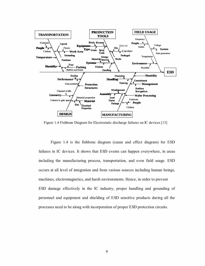
Figure 1.4 is the fishbone diagram (cause and effect diagram) for ESD
failures in IC devices. It shows that ESD events can happen everywhere, in areas
including the manufacturing process, transportation, and even field usage. ESD
occurs at all level of integration and from various sources including human beings,
machines, electromagnetics, and harsh environments. Hence, in order to prevent
ESD damage effectively in the IC industry, proper handling and grounding of
personnel and equipment and shielding of ESD sensitive products during all the
processes need to be along with incorporation of proper ESD protection circuits.
ESD
EnvironmentHumidity
People
System
FIELD USAGE
Voltage
Heat generation
Habits
Temperature
Frequency
People
Size ElectricalProperties
LeadFrame
Misalignment
Training
Discipline
Package
Furniture
Layout
FloorsClothes
Blowers
Humidity
Material
Geometry
Management
Assembly
Handling
Work Area
EquipmentType
MANUFACTURINGDESIGN
PRODUCTIONTOOLSTRANSPORTATION
Structures
Commitment
ProblemRecognition
Temperature
Scaling
Gate potential
Systems
Handling
Materials
Footware
Grounding
Brush
SprayTools
Ovens
Wafer
Die
PackagedEnergy Sources
Friction
People
Material properties
Size ElectricalProperties
LeadFrame
Misalignment
Training
Discipline
Package
Furniture
Layout
Bags
Clothes
Blowers
Humidity
Material
Humidity
Assembly
Handling
Packing
EquipmentType
DESIGN
ProtectionCommitment
ProblemRecognition
Scaling
Channel width
Systems
Handling
Wafer Processing
Materials
Footware
Grounding
Brush
SprayTools
Ovens
Wafer
Die
PackagedEnergy Sources
Friction
Contact to gate space
Performance
People
Bubble and foam
Material
Carriers
ESD
EnvironmentHumidity
People
System
FIELD USAGE
Voltage
Heat generation
Habits
Temperature
Frequency
People
Size ElectricalProperties
LeadFrame
Misalignment
Training
Discipline
Package
Furniture
Layout
FloorsClothes
Blowers
Humidity
Material
Geometry
Management
Assembly
Handling
Work Area
EquipmentType
MANUFACTURINGDESIGN
PRODUCTIONTOOLS
PRODUCTIONTOOLSTRANSPORTATION
Structures
Commitment
ProblemRecognition
Temperature
Scaling
Gate potential
Systems
Handling
Materials
Footware
Grounding
Brush
SprayTools
Ovens
Wafer
Die
PackagedEnergy Sources
Friction
People
Material properties
Size ElectricalProperties
LeadFrame
Misalignment
Training
Discipline
Package
Furniture
Layout
Bags
Clothes
Blowers
Humidity
Material
Humidity
Assembly
Handling
Packing
EquipmentType
DESIGN
ProtectionCommitment
ProblemRecognition
Scaling
Channel width
Systems
Handling
Wafer Processing
Materials
Footware
Grounding
Brush
SprayTools
Ovens
Wafer
Die
PackagedEnergy Sources
Friction
Contact to gate space
Performance
People
Bubble and foam
Material
Carriers
Figure 1.4 Fishbone Diagram for Electrostatic discharge failures on IC devices [13]
10
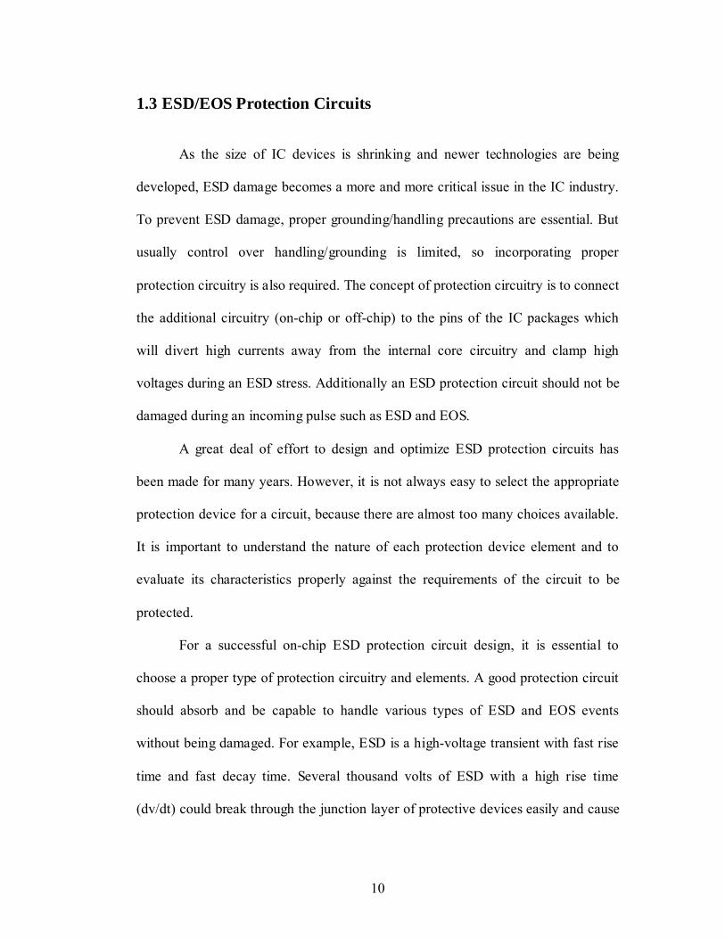
1.3 ESD/EOS Protection Circuits
As the size of IC devices is shrinking and newer technologies are being
developed, ESD damage becomes a more and more critical issue in the IC industry.
To prevent ESD damage, proper grounding/handling precautions are essential. But
usually control over handling/grounding is limited, so incorporating proper
protection circuitry is also required. The concept of protection circuitry is to connect
the additional circuitry (on-chip or off-chip) to the pins of the IC packages which
will divert high currents away from the internal core circuitry and clamp high
voltages during an ESD stress. Additionally an ESD protection circuit should not be
damaged during an incoming pulse such as ESD and EOS.
A great deal of effort to design and optimize ESD protection circuits has
been made for many years. However, it is not always easy to select the appropriate
protection device for a circuit, because there are almost too many choices available.
It is important to understand the nature of each protection device element and to
evaluate its characteristics properly against the requirements of the circuit to be
protected.
For a successful on-chip ESD protection circuit design, it is essential to
choose a proper type of protection circuitry and elements. A good protection circuit
should absorb and be capable to handle various types of ESD and EOS events
without being damaged. For example, ESD is a high-voltage transient with fast rise
time and fast decay time. Several thousand volts of ESD with a high rise time
(dv/dt) could break through the junction layer of protective devices easily and cause
11
damage. However, ESD surge energy is very small and it does not require much
energy-handling capability from a protective device. One the other hand, EOS is a
much slower phenomenon than ESD but much larger energy is involved. The
following factors need be considered for designing an ideal protection device for
EOS and ESD [14];
• Voltage-clamping devices should limit the surge voltage to a safe level for the
circuit or component being protected.
• Voltage-clamping devices should withstand several thousand volts in a fast
dv/dt impulse.
• Protective devices should be small enough to fit into a limited space on a
printed circuit board (PCB). Most components that require ESD protection are
small surface-mount devices (SMD).
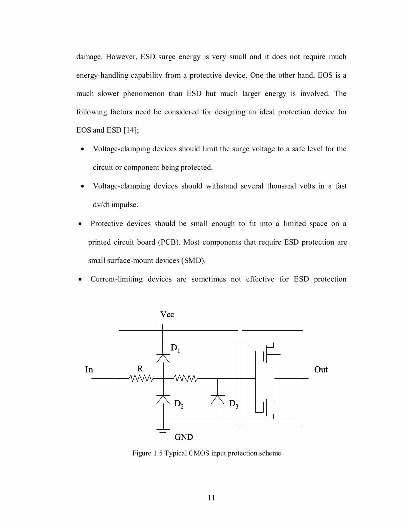
• Current-limiting devices are sometimes not effective for ESD protection
D1
D2 D3
In R Out
Vcc
GND
D1
D2 D3
In R Out
Vcc
GND Figure 1.5 Typical CMOS input protection scheme

12
because ESD current is very small and does not induce much voltage across the
device.
• Limiting devices with high impedance are not effective for ESD protection. The
stray capacitance in these devices could provide low reactance.
Relying upon on-chip protection to suppress ESD/EOS events may provide a
false sense of security if not carefully evaluated. In the past, 2kV-4kV of on-chip
ESD protection was thought to be adequate protection, but new standards such as
IEC 61000-4-2 have raised the minimum protection level to as much as 15kV. As
device geometries continue to shrink, it is becoming more difficult to add on-chip
protection with a common manufacturing process. As a result, devices operating at
low voltages may not be adequately protected.
Some integrated circuits feature built in protection by means of an internal
SCR (silicon controlled rectifier) or resistor and diode network. The basic
requirements of a protection network are that it provides a low impedance path for
the discharge energy while limiting the current and voltage seen by the active circuit.
This means that the transient energy is dissipated in the protection network itself.
The basic input protection circuit usually consists of the following elements:
• A shunt device to discharge positive polarity transients
• A shunt device to discharge negative polarity transients
• A series element for current limiting
A typical CMOS input protection circuit is shown in Figure 1.5. When an
ESD voltage is applied to the input structure, the on-chip diodes shunt the transient
current to the power line (Vcc) or ground. A positive transient voltage causes diode

13
D1 to be forward biased when the input voltage exceeds Vcc. Likewise, for negative
transients, diode D2 shunts the negative current. The polysilicon input resistors serve
to limit the peak currents. Since polysilicon resistors are thermally insulated by a
surrounding layer of SiO2 or glass, they are particularly susceptible to thermal
damage resulting from joule heating by ESD induced currents. A typical CMOS
input protection circuit can provide ESD immunity to approximately 4kV [15].

14
2. ESD CHARACTERIZATION IN IC DEVICES
In this chapter, a general overview of the characterization of ESD
phenomena as preliminary information for this dissertation is presented. The
ESD/EOS induced failure mode, basic device physics to explain ESD/EOS related
failure mechanisms, and the overview of ESD test models are provided as well.
For mathematical models of ESD/EOS induced failures, modeling
techniques have been proposed for failure mechanisms involved with semiconductor,
oxide and metallization failures. Selected approaches are included in this chapter as
well as the primary mechanisms associated with ESD and EOS.
In order to characterize the susceptibility of an IC to ESD damage, the IC
must be tested using models which accurately simulate real ESD events. These
models should be standardized so that testing is consistent and reliability can be
defined quantitatively. Actual ESD stresses occur during wafer fabrication,
packaging, testing, or any other time the circuit comes in contact with a person or
machine. The majority of stresses occur between two pins of an IC package when
the chip is not powered up, a fact reflected in the setup of ESD characterization tests
[17]. Specific tests are designed to model specific events such as human handling,
machine handling, and field induction.
The most common industrial tests used to measure ESD robustness are the
human-body model (HBM), the machine model (MM), and the charged-device
model (CDM) [18]-[20]. These most common models will be explained in detail in
this chapter together with other models. Briefly, the human-body model consists of
15
charging a capacitor to a high voltage and then discharging the capacitor through a
series resistor into the pins of a packaged IC with another pin grounded and all other
pins floating. HBM testing is often the sole means of qualifying ESD reliability
because the specifications of the test are standardized industry wide and because
several commercial HBM testers are available.
Similarly to the HBM, in the machine model a capacitor is charged up to a
high voltage and then discharged through the pins of an IC. Unlike the HBM, the
MM discharges the capacitor through only a very small, parasitic series resistance,
resulting in an oscillatory input pulse comparable to a pulse generated by a charged
metal machine part contacting an IC pin.
The CDM test, which consists of charging a ground pin of a package using a
voltage source, removing the voltage source, and then discharging the package by
shorting a different pin, is meant to simulate the electrostatic charging of a package
due to improper grounding and its subsequent discharging when a low-resistance
path becomes available.
2.1 Basic Device Physics
Before examining failure mechanisms caused by ESD, a brief overview of
some device physics is useful to understand ESD failure phenomena. When silicon
is heated, the carriers normally present in the device are supplemented by thermally
generated carriers. This causes the resistivity of silicon to decrease sharply with an
increase in temperature, as shown in Figure 2.1. This is known as Runyan’s curve.

16
Additionally, Figure 2.2 shows that increasing the temperature of silicon causes its
thermal conductivity to decrease.
Room temperature
Temperature (0C)
Ther
mal
con
duct
ivity Room temperature
Temperature (0C)
Ther
mal
con
duct
ivity
Figure 2.1 Decrease in thermal conductivity of silicon with increasing temperature [25]
Room temperature
Temperature (0C)
Resis
tivity
0 200 400
Room temperature
Temperature (0C)
Resis
tivity
0 200 400
Figure 2.2 A rapid decrease in resistivity of doped silicon with increasing temperature [25]

17
Combining the effects shown in the two figures, some conclusions about the
thermo-mechanical behavior of silicon may be reached. When energy is suddenly
dumped into a silicon device in the form of an ESD impulse, the heating of the
silicon is inherently uneven. A small area of the junction will absorb current and
heat up, causing its resistivity to drop sharply. Once heating is taking place the small
area becomes effectively thermally isolated from its surroundings because the
thermal conductivity of the silicon decreases. This effect is a positive feedback
mechanism resulting in damage to the device known variously as a punchthrough or
a meltthrough.
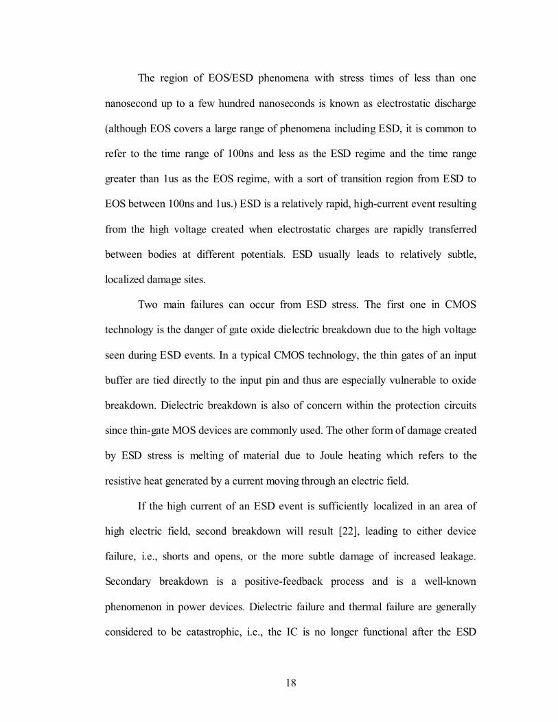
2.2 ESD/EOS Induced-Failure Mode and Mechanism
Electrical overstress (EOS) is defined as damage to a product caused by
exceeding maximum ratings. EOS usually leads to catastrophic damages in
integrated circuits resulting from high-energy events such as electrostatic discharge,
electromagnetic pulses, lightning, or reversal of power and ground pins. EOS failure
mechanisms fall into the two broad categories of thermally induced failures and
high electric-field failures. The duration of an EOS event may be anywhere from
less than one nanosecond to one millisecond and longer. Long EOS events can lead
to damaged areas such as blown metal lines, cavities in the silicon, or discoloration
of silicon due to local heating with a characteristic radius of 100um or greater. This
damage leads to either a reduction in IC performance (e.g., increased leakage
current on one or more pines) or total circuit failure [21].
18
The region of EOS/ESD phenomena with stress times of less than one
nanosecond up to a few hundred nanoseconds is known as electrostatic discharge
(although EOS covers a large range of phenomena including ESD, it is common to
refer to the time range of 100ns and less as the ESD regime and the time range
greater than 1us as the EOS regime, with a sort of transition region from ESD to
EOS between 100ns and 1us.) ESD is a relatively rapid, high-current event resulting
from the high voltage created when electrostatic charges are rapidly transferred
between bodies at different potentials. ESD usually leads to relatively subtle,
localized damage sites.
Two main failures can occur from ESD stress. The first one in CMOS
technology is the danger of gate oxide dielectric breakdown due to the high voltage
seen during ESD events. In a typical CMOS technology, the thin gates of an input
buffer are tied directly to the input pin and thus are especially vulnerable to oxide
breakdown. Dielectric breakdown is also of concern within the protection circuits
since thin-gate MOS devices are commonly used. The other form of damage created
by ESD stress is melting of material due to Joule heating which refers to the
resistive heat generated by a current moving through an electric field.
If the high current of an ESD event is sufficiently localized in an area of
high electric field, second breakdown will result [22], leading to either device
failure, i.e., shorts and opens, or the more subtle damage of increased leakage.
Secondary breakdown is a positive-feedback process and is a well-known
phenomenon in power devices. Dielectric failure and thermal failure are generally
considered to be catastrophic, i.e., the IC is no longer functional after the ESD

19
stress. However, as has been noted there is another type of ESD damage referred to
as latent damage. Latent damage consists of increased leakage current or reduced
oxide integrity, without loss of functionality. A latent ESD failure is defined as
“malfunction that occurs in use conditions because of earlier exposure to ESD that
did not result in an immediately detectable discrepancy” [23]. Latent damage is
often bake-recoverable. Low-level leakage (an increase in leakage which remains
below the failure threshold), also referred to as soft failure, may be due to injection
of hot carriers into the gate oxide, which would cause a threshold voltage shift, or to
damage in the silicon resulting from localized melting, or to both. A small damage
site could act like a high-resistance filament across a diode junction, thereby
increasing the leakage current to a significant but non-catastrophic level. Polgreen et
al. [24] found this to be true for MOSFETs with pulse widths below a certain critical
value. They postulated that a certain amount of total current is needed to cause
widespread device damage. Extensive damage will not occur until the device is
driven deeper into second breakdown by being stressed with a higher current.
During pulsed overstress, carriers are generated by avalanche multiplication.
This thermally driven impact generation process occurs much faster than carrier
generation during normal device operation. Thermal propagation is relatively slow
compared to the avalanche breakdown mechanism, confining the heat generated to a
small region of the device. Taken together, this results in current filamentation,
shown in Figure 2.3. With repeated pulsing, a hot spot will develop because heat is
being generated faster at the generation site than it can be dissipated.

20
In bipolar transistors, the base injection no longer controls the collector
current, and the device is in thermal runaway. The mobility decreases with impurity
concentration and decreases with increasing temperature. Depending on circuit
conditions, the hot spot may also quickly develop temperatures at which the
aluminum and silicon form an alloy, and the device is quickly shorted and
destroyed.
Fused metal
Silicon melting
Fused metal
Silicon melting
Figure 2.3 Cross sectional drawing of ESD damage in bipolar structures [25]
Gate oxide rupture
Gate metal fusing
Gate oxide rupture
Gate metal fusing
Figure 2.4 Cross sectional drawing of ESD damage in MOS structures [25]
21
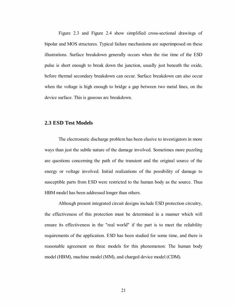
Figure 2.3 and Figure 2.4 show simplified cross-sectional drawings of
bipolar and MOS structures. Typical failure mechanisms are superimposed on these
illustrations. Surface breakdown generally occurs when the rise time of the ESD
pulse is short enough to break down the junction, usually just beneath the oxide,
before thermal secondary breakdown can occur. Surface breakdown can also occur
when the voltage is high enough to bridge a gap between two metal lines, on the
device surface. This is gaseous arc breakdown.
2.3 ESD Test Models
The electrostatic discharge problem has been elusive to investigators in more
ways than just the subtle nature of the damage involved. Sometimes more puzzling
are questions concerning the path of the transient and the original source of the
energy or voltage involved. Initial realizations of the possibility of damage to
susceptible parts from ESD were restricted to the human body as the source. Thus
HBM model has been addressed longer than others.
Although present integrated circuit designs include ESD protection circuitry,
the effectiveness of this protection must be determined in a manner which will
ensure its effectiveness in the "real world" if the part is to meet the reliability
requirements of the application. ESD has been studied for some time, and there is
reasonable agreement on three models for this phenomenon: The human body
model (HBM), machine model (MM), and charged device model (CDM).

22
Human Body Model (HBM) [18]
Under various conditions, the human body can be charged with electrical
energy and transfer that charge to a semiconductor device through normal handling
or assembly operations. To evaluate the effectiveness of the protection circuitry in
Figure 2.5 HBM ESD waveform at 500 V, short circuit [26]
Figure 2.6 HBM test circuit [26]
23
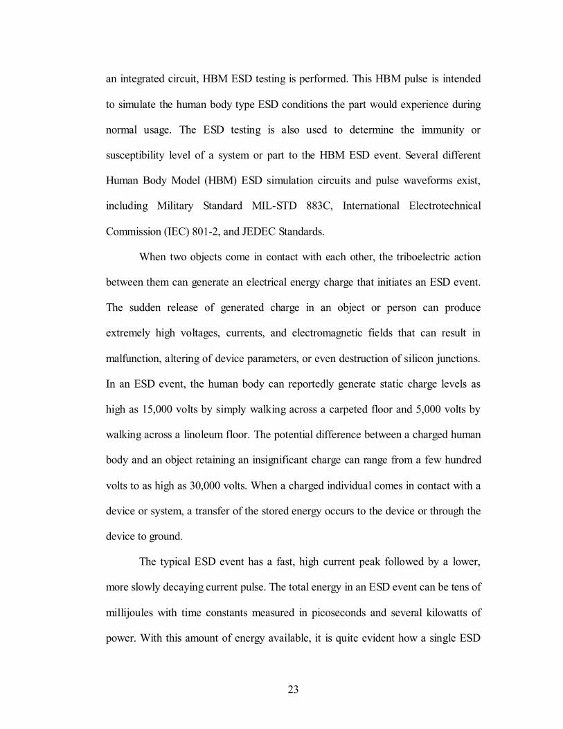
an integrated circuit, HBM ESD testing is performed. This HBM pulse is intended
to simulate the human body type ESD conditions the part would experience during
normal usage. The ESD testing is also used to determine the immunity or
susceptibility level of a system or part to the HBM ESD event. Several different
Human Body Model (HBM) ESD simulation circuits and pulse waveforms exist,
including Military Standard MIL-STD 883C, International Electrotechnical
Commission (IEC) 801-2, and JEDEC Standards.
When two objects come in contact with each other, the triboelectric action
between them can generate an electrical energy charge that initiates an ESD event.
The sudden release of generated charge in an object or person can produce
extremely high voltages, currents, and electromagnetic fields that can result in
malfunction, altering of device parameters, or even destruction of silicon junctions.
In an ESD event, the human body can reportedly generate static charge levels as
high as 15,000 volts by simply walking across a carpeted floor and 5,000 volts by
walking across a linoleum floor. The potential difference between a charged human
body and an object retaining an insignificant charge can range from a few hundred
volts to as high as 30,000 volts. When a charged individual comes in contact with a
device or system, a transfer of the stored energy occurs to the device or through the
device to ground.
The typical ESD event has a fast, high current peak followed by a lower,
more slowly decaying current pulse. The total energy in an ESD event can be tens of
millijoules with time constants measured in picoseconds and several kilowatts of
power. With this amount of energy available, it is quite evident how a single ESD
24
event can result in a device failure or possibly initiate a device weakness that can
cause failure with continued use.
Recent research on human body ESD events shows that discharge pulses
with fast rise times, on the order of 1 nanosecond or less, are the most disruptive to
the normal operation of electronic equipment. Therefore, ESD test systems using a
fast rise time pulse will more accurately simulate the human body discharge events
frequently encountered. Measurement of these parameters has been difficult due
primarily to the short time interval, large potential differences, and the measurement
bandwidth required to capture both the amplitude and frequency characteristics of
the ESD event. These limitations may cloud the issues of ESD susceptibility levels
and environmental factors which may protect or damage electronic devices.
The simplest human body ESD model is the series RLC circuit shown in
figure above in which the R corresponds to the body resistance, L is the
corresponding body inductance, and C is the capacitance of the body with respect to
its surroundings. The body inductance is often neglected, as in MIL-STD 883C,
while a body capacitance of 100 to 250 pF and body resistance of 1000 to 2000
ohms is generally used.
Machine Model (MM) [19]
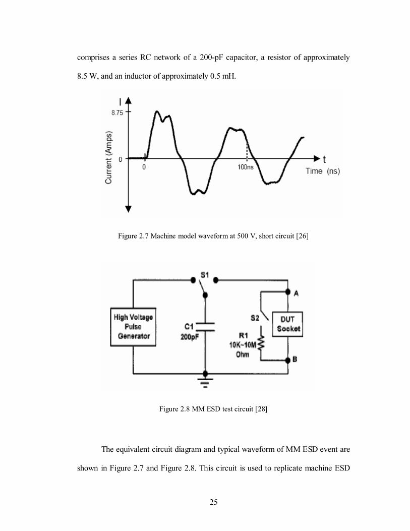
The Machine Model is designed to simulate a machine (test equipment,
furniture, etc.) discharging accumulated static charge through a device to ground. It
25
comprises a series RC network of a 200-pF capacitor, a resistor of approximately
8.5 W, and an inductor of approximately 0.5 mH.
Figure 2.7 Machine model waveform at 500 V, short circuit [26]
Figure 2.8 MM ESD test circuit [28]
The equivalent circuit diagram and typical waveform of MM ESD event are
shown in Figure 2.7 and Figure 2.8. This circuit is used to replicate machine ESD

26
events in semiconductor devices. Usually, a commercial IC is requested to sustain at
least 200 V MM ESD stress. A 200 V MM ESD event can generate an ESD current
peak of up to 3.5A with a rise time up to 10ns. The ESD damage to an IC caused by
MM ESD stress is similar to that caused by HBM ESD stress, but it occurs at a
significantly lower voltage. Typically, the ratio between HBM ESD robustness and
MM ESD robustness of the same IC product is about 8~12. But little research has
been done to correlate both ESD test models.
The primary MM standards are known as JEDEC EIA/JESD22-A115-A and
ESDA STM 5.2-1999. The JEDEC EIA/JESD22-A115-A was developed and
released in 1994 for eliminating flaws in the EIAJ test method. The ESDA ESD
STM 5.2 1999 was developed in early 90’s. Recently, the ESDA MM device testing
working group reviewed the results of additional round-robin testing using a
reduced number of pulses per stress level (1 pulse instead of 5). The results obtained
thus far reveal inconsistent failure thresholds. Further investigation into waveform
parameters revealed large variations while meeting standard requirements.
Charged Device Model (CDM) [20]
In 1974, Speakman [27] proposed the possibility of destroying an electronic
part, such as an integrated circuit, by rapid discharge of accumulated static on a
part’s own body. This type of failure has since been called the charged device model
(CDM) failure. The CDM ESD test is schematically drawn with the device in Figure
2.9 and a typical waveform is shown in Figure 2.10. In this CDM ESD event, the

27
ESD static charges are initially stored in the body of a floating IC. Most of the CDM
charges are initially stored in the body of an IC device.
Figure 2.9 CDM ESD test setup
Figure 2.10 Typical current waveform from CDM
When some pin of this charged IC is touched by an external ground, the
stored charged will be discharged from the inside of the IC to the outside ground. In
the CDM ESD test setup (Figure 2.9), the IC is initially charged by the field-induced
method without the socket, and then discharged through a grounded metal probe.

28
The IC is initially charged by the direct connection to the high voltage source
through the IC socket, and then discharge through the switch and the socket of the
tester to ground. Usually a commercial IC is requested to sustain at least 1 kV CDM
ESD stress. The typical 1 kV CDM ESD event from a charged IC (with an
equivalent 4pF capacitance to ground) can generate a current peak as high as 15A
within a rise time of only around 200ps. With such a large ESD current and so fast a
transition time, the I/O devices in CMOS IC’s are totally destroyed by such ESD
currents [28]. The primary CDM standards are ESDA STM 5.3.1-1999 and
JESD22-C101A. The original CDM waveform and subsequent test system was
designed by Bossard [29] in 1980. This architecture and waveform was the basis for
the development of the JESD22-C101-A. Besides, the ESDA began development on
its own method (ESD STM 5.3.1 & ESD STM 5.3.2).
Limitation of present ESD test methods
A discrepancy appears to exist between reality, measured reality, and
common practice as defined in some industry specifications. We feel a universally
accepted specification defining the actual ESD waveform is not presently available
due to various factors including:
1. The non-uniform conditions involved in the ESD environment.
2. The unpredictable circumstances of the ESD event.
3. The constant improvement in test equipment used to study the ESD event.

29
4. Supplier community resistance to adopting new standards that would
indicate some currently used protection circuits are inadequate.
5. Lack of a standardized procedure for capturing the ESD event. Some
procedures use measurement techniques that are not capable of capturing the high
frequency content or fast rise time of the waveform.
Previous investigations into ESD testing have resulted in two conflicting
philosophies. One philosophy states, "The test procedure must look like a human
ESD spark...including all variability observed in natural ESD phenomena". The
second testing philosophy is to choose a representative waveform from the range of
likely ESD events and generate an instrumentation approach to ESD testing. This
latter ESD testing philosophy employs test systems designed to produce a consistent
and repeatable ESD waveform.
The difficulty with ESD test systems has been the inability to deliver the
relatively fast risetime associated with the surface charge stored on the human body.
Many test systems incorporate lumped time constant circuitry and are plagued by
parasitic inductance, resistance, and capacitance of the various components. These
parasitics can greatly affect the response of the ESD test system and therefore result
in invalid ESD event rise times. The measured rise times are also limited by the
capabilities of the measurement equipment used to capture the ESD event
waveform. When the MIL-STD 883C testing procedure was released in 1989, the
risetime stated as less than 10 ns may have been accurate for the type of equipment
available for waveform verification. Measurement equipment presently available is

30
capable of detecting and capturing ESD waveforms with rise times as fast as a few
hundred picoseconds [30].
Other models
The socketed CDM (SCDM) test method is basically similar to CDM. This
model simulates a charged IC coming into contact with a low impedance conductive
surface. The device under test is placed in a socket, charged from a high-voltage
source, and then discharged. The SCDM test enhances the package parasitics by
placing the device in a socket, mounted on a test fixture board, and connected via
pogo pins to a relay switching matrix. Since the device itself is not in intimate
contact with a ground plane, the stored energy is located on the tester components,
associated with wiring, and to a much less degree, is located in the device socket
[31].
The field induced charged device model (FCDM) is also known as indirect
ESD. This type of ESD is not completely characterized, but it is generated by an
electrostatic field, which is created by the discharge of an ESD pulse. It is similar to
an EMI field which can induce a voltage and current on a data or power line. The
transient that is induced on the line or PCB trace is conducted into the IC
component. The level of ESD induced depends upon the length of the printed circuit
board (PCB) traces. Induced ESD effects are more PCB dependent and need to be
characterized by circuit/system design engineers [32].

31
ESD sensitivity classification levels
A set of test procedures explained above is normally used to evaluate the
ESD 'immunity' of a component, i.e., to evaluate the magnitude of an ESD discharge
that a component can absorb without permanent damage.
Different IC device technologies and different applications have different
levels of immunity to electrical stress such as ESD and EOS. So, there needs to be a
convenient classification to differentiate ESD-sensitive devices from those which
are not as vulnerable to ESD. Each of the ESD models used in ESD sensitivity
testing has its own classification system for categorizing devices according to their
ESD sensitivity. The ESD sensitivity of a device is usually specified in terms of the
highest ESD test voltage that it passes and the lowest ESD test voltage that it fails
per ESD model. Thus, ESD sensitivity is often expressed as a range of ESD voltage
Table 2.1 ESD immunity classification Class Voltage Range
0 < 250 volts
1A 250 volts to < 500 volts
1B 500 volts to < 1,000 volts
1C 1000 volts to < 2,000 volts
2 2000 volts to < 4,000 volts
3A 4000 volts to < 8000 volts
3B > = 8000 volts
Class Voltage Range
M1 < 100 volts
M2 100 volts to < 200 volts
M3 200 volts to < 400 volts
M4 > or = 400 volts
Class Voltage Range
C1 <125 volts
C2 125 volts to < 250 volts
C3 250 volts to < 500 volts
C4 500 volts to < 1,000 volts
C5 1,000 volts to < 1,500 volts
C6 1,500 volts to < 2,000 volts
C7 =>2,000 volts
[ Human Body Model ] [ Machine Model ] [ Charged Device Model ]
Class Voltage Range
0 < 250 volts
1A 250 volts to < 500 volts
1B 500 volts to < 1,000 volts
1C 1000 volts to < 2,000 volts
2 2000 volts to < 4,000 volts
3A 4000 volts to < 8000 volts
3B > = 8000 volts
Class Voltage Range
0 < 250 volts
1A 250 volts to < 500 volts
1B 500 volts to < 1,000 volts
1C 1000 volts to < 2,000 volts
2 2000 volts to < 4,000 volts
3A 4000 volts to < 8000 volts
3B > = 8000 volts
ClassClassClass Voltage RangeVoltage RangeVoltage Range
00 < 250 volts< 250 volts
1A1A 250 volts to < 500 volts
250 volts to < 500 volts
1B1B 500 volts to < 1,000 volts
500 volts to < 1,000 volts
1C1C 1000 volts to < 2,000 volts
1000 volts to < 2,000 volts
22 2000 volts to < 4,000 volts
2000 volts to < 4,000 volts
3A3A 4000 volts to < 8000 volts
4000 volts to < 8000 volts
3B3B > = 8000 volts> = 8000 volts
Class Voltage Range
M1 < 100 volts
M2 100 volts to < 200 volts
M3 200 volts to < 400 volts
M4 > or = 400 volts
Class Voltage Range
M1 < 100 volts
M2 100 volts to < 200 volts
M3 200 volts to < 400 volts
M4 > or = 400 volts
ClassClassClass Voltage RangeVoltage RangeVoltage Range
M1M1 < 100 volts< 100 volts
M2M2 100 volts to < 200 volts
100 volts to < 200 volts
M3M3 200 volts to < 400 volts
200 volts to < 400 volts
M4M4 > or = 400 volts> or = 400 volts
Class Voltage Range
C1 <125 volts
C2 125 volts to < 250 volts
C3 250 volts to < 500 volts
C4 500 volts to < 1,000 volts
C5 1,000 volts to < 1,500 volts
C6 1,500 volts to < 2,000 volts
C7 =>2,000 volts
Class Voltage Range
C1 <125 volts
C2 125 volts to < 250 volts
C3 250 volts to < 500 volts
C4 500 volts to < 1,000 volts
C5 1,000 volts to < 1,500 volts
C6 1,500 volts to < 2,000 volts
C7 =>2,000 volts
ClassClassClass Voltage RangeVoltage RangeVoltage Range
C1C1 <125 volts<125 volts
C2C2 125 volts to < 250 volts
125 volts to < 250 volts
C3C3 250 volts to < 500 volts
250 volts to < 500 volts
C4C4 500 volts to < 1,000 volts
500 volts to < 1,000 volts
C5C5 1,000 volts to < 1,500 volts
1,000 volts to < 1,500 volts
C6C6 1,500 volts to < 2,000 volts
1,500 volts to < 2,000 volts
C7C7 =>2,000 volts=>2,000 volts
[ Human Body Model ] [ Machine Model ] [ Charged Device Model ]
32
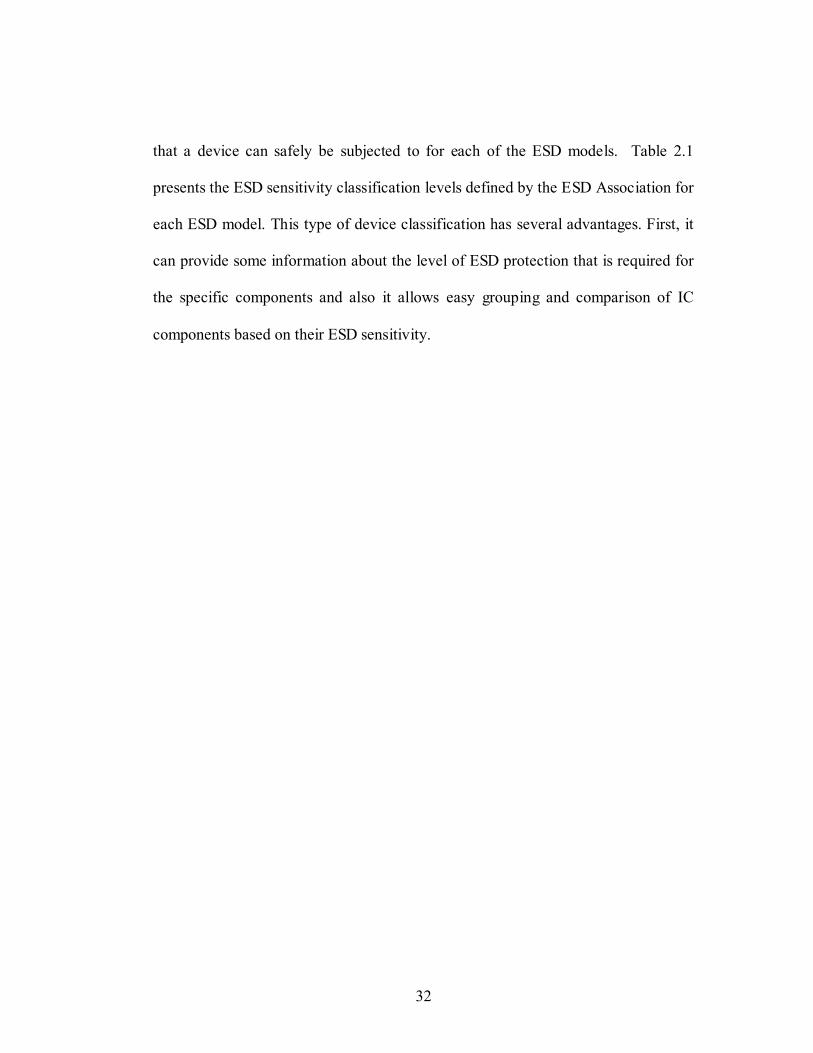
that a device can safely be subjected to for each of the ESD models. Table 2.1
presents the ESD sensitivity classification levels defined by the ESD Association for
each ESD model. This type of device classification has several advantages. First, it
can provide some information about the level of ESD protection that is required for
the specific components and also it allows easy grouping and comparison of IC
components based on their ESD sensitivity.
33
3. OBJECTIVES AND OUTLINE OF THIS THESIS
The objective of this study is to clarify ESD/EOS events experimentally and
theoretically and their effects on non-silicon semiconductor devices (GaAs and SiGe
devices) due to the high voltage and current. In order to study ESD/EOS
phenomena, extensive experiments would have been conducted, and an analytical
model for failure on IC devices will be developed. The specific experimental and
modeling objectives of this dissertation are to research some key questions. The
questions are listed below.
1. Can one differentiate ESD and EOS induced failures and develop a root
cause analysis process to assess ESD/EOS induced field failures?
2. Are there differences in the failure signatures, based on the ESD models for
non-silicon IC devices?
3. Can one reproduce field failures by EOS and several ESD test models?
4. What is the latent damage effect on GaAs MESFET devices?
5. Is there an acceptable model for failures caused by ESD conditions?
Chapter 1 and 2 presents a general overview of the characterization of the
ESD and EOS phenomena as preliminary information for better understanding of
this dissertation. The generation of ESD, the effect of ESD on electronics, type of
ESD-induced failure mode and mechanisms are provided. A brief overview of ESD
test models for replicating real ESD is presented as well.

34
Chapter 4 and chapter 5 addresses characterization and analysis for the
failures caused by ESD/EOS and field returned devices. The detailed procedure for
root cause analysis is documented with two case studies for SiGe and GaAs device.
The failure site and signature resulting from different stress conditions are also
documented and compared with those of field failures
In chapter 6, the effect of latent damage on GaAs devices is evaluated.
Experimental procedures and electrical/physical characteristics after low-level ESD
stress are presented. The difference of failure signatures resulting from different
electrical stress levels through a detailed failure analysis is also documented. The
effect of ESD stress below the threshold of hard failure to the susceptibility of the
device to subsequent electrical overstress is also presented. The failure signatures
from various types of ESD, EOS, and EOS-ESD combined stress are presented as
well and a possible screening method is proposed.
An application and development of an ESD failure model using a thermal
RC network to predict the power-to-failure level is presented in chapter 7, starting
with a general discussion of the development procedure of the analytical model. A
review of some previous prediction work and their comparison is also given. The
effect of device parameters and power-to-failure comparison are also evaluated
using a numerical model. Based on the analytical prediction model developed, the

35
correlation of HBM ESD stress and square wave pulse is presented and the issue of
HBM equivalent square wave pulse duration is discussed.

36
4. FAILURE ANALYSIS AND ESD EVALUATION
OF SiGe OPAMPS
In this chapter, Silicon-Germanium (SiGe) BiCMOS RF OpAmp devices
have been investigated for electrostatic discharge (ESD) evaluation. ESD evaluation
is particularly important in high-frequency RF wireless applications because the
ESD immunity level in RF devices is comparatively lower than other devices. Also,
application of ESD protection circuits or components for RF devices is not simple
due to their unique characteristics.
During this evaluation, the human body model, machine model, and charged
device model electrostatic discharge test models were applied to create ESD-
induced failures. Failure mode and effect analysis, visual inspection, electrical tests,
X-ray observation, liquid crystal application, focused ion beam examination, optical
microscopy, and scanning electron microscopy inspection were performed on ESD-
failed SiGe BiCMOS OpAmp RF devices. This study shows that the failure
locations and damage shapes varied, depending upon how the failures are created.
Results of failure analysis under different stress conditions are compared.
4.1 SiGe devices and ESD
Silicon-Germanium (SiGe) BiCMOS is a silicon technology that combines a
high-performance heterojunction bipolar transistor (HBT) with advanced CMOS
technology. Applications of SiGe technology are most important in microwave
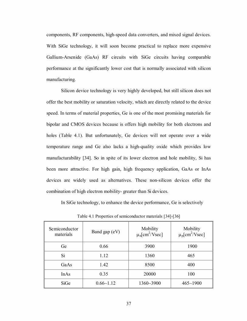
37
components, RF components, high-speed data converters, and mixed signal devices.
With SiGe technology, it will soon become practical to replace more expensive
Gallium-Arsenide (GaAs) RF circuits with SiGe circuits having comparable
performance at the significantly lower cost that is normally associated with silicon
manufacturing.
Silicon device technology is very highly developed, but still silicon does not
offer the best mobility or saturation velocity, which are directly related to the device
speed. In terms of material properties, Ge is one of the most promising materials for
bipolar and CMOS devices because is offers high mobility for both electrons and
holes (Table 4.1). But unfortunately, Ge devices will not operate over a wide
temperature range and Ge also lacks a high-quality oxide which provides low
manufacturability [34]. So in spite of its lower electron and hole mobility, Si has
been more attractive. For high gain, high frequency application, GaAs or InAs
devices are widely used as alternatives. These non-silicon devices offer the
combination of high electron mobility- greater than Si devices.
In SiGe technology, to enhance the device performance, Ge is selectively
Table 4.1 Properties of semiconductor materials [34]-[36]
Semiconductor materials Band gap (eV) Mobility
µn[cm2/Vsec] Mobility
µp[cm2/Vsec]
Ge 0.66 3900 1900
Si 1.12 1360 465
GaAs 1.42 8500 400
InAs 0.35 20000 100
SiGe 0.66~1.12 1360~3900 465~1900

38
introduced into the base region of the transistor. The smaller base bandgap of SiGe
compared to Si enhances electron injection, producing a higher current gain for the
same base doping level compared to a Si device. As shown in Figure 4.1 (a),
compared to a Si device, a SiGe device has better characteristics of high speed and
low power consumption which means it is more suitable for high speed RF
applications. For example, A SiGe transistor has up to 1.5 times higher peak
frequency and up to 7 times lower power consumption for the same frequency as
compared to a silicon based transistor [35]. One more advantage of a SiGe device is
its cost. As shown Figure 4.1(b), the cost of a chip in SiGe is comparable to that of
Si devices and performance of SiGe devices is comparable to GaAs devices which
is essential in applications where a particular circuit function cannot be
accomplished with silicon devices [36]. So SiGe devices are aimed at replacing
silicon devices in RF and microwave components. A heterojunction bipolar
transistor with SiGe technology was first demonstrated in 1988. The Si/SiGe system
was developed using molecular beam epitaxy [37]-[39]. Molecular beam epitaxy
Figure 4.1 Advantages of SiGe devices
39
(MBE) is a controlled thermal evaporation process under ultrahigh vacuum
conditions where a substrate is held in high vacuum while molecular or atomic
beams of the constituents impinge on its surface.
Products utilizing SiGe technology undergo essentially the same product
reliability stressing as products using bulk Si. Typical reliability test activities
include high temperature operating life (HTOL) at 125 oC for 1000 hours, with DC
and functional tests performed at 0 and 1000 hours. ESD testing is also included for
both the human body model and charged device model; latch-up characterization is
also completed [40].
With the increased volume and growth in the applications that use SiGe
BiCMOS devices, the ESD sensitivity characterization of SiGe BiCMOS devices
has become more important [41]. ESD evaluation is particularly important in high-
frequency RF wireless applications. This is because damage from ESD/EOS is
usually caused by localized overheating, which implies ESD robustness of devices
is a strong function of the material melting temperature and thermal conductivity.
Due to the low thermal conductivity and low melting temperature of SiGe, SiGe
devices are more sensitive to ESD than Si devices. Furthermore, application of ESD
protection circuit or components for RF devices is not simple due to its own unique
characteristics. In this study, HBM, MM, and CDM testing for an epitaxial base
SiGe device were carried out on all possible pin connections in order to duplicate
ESD failures.
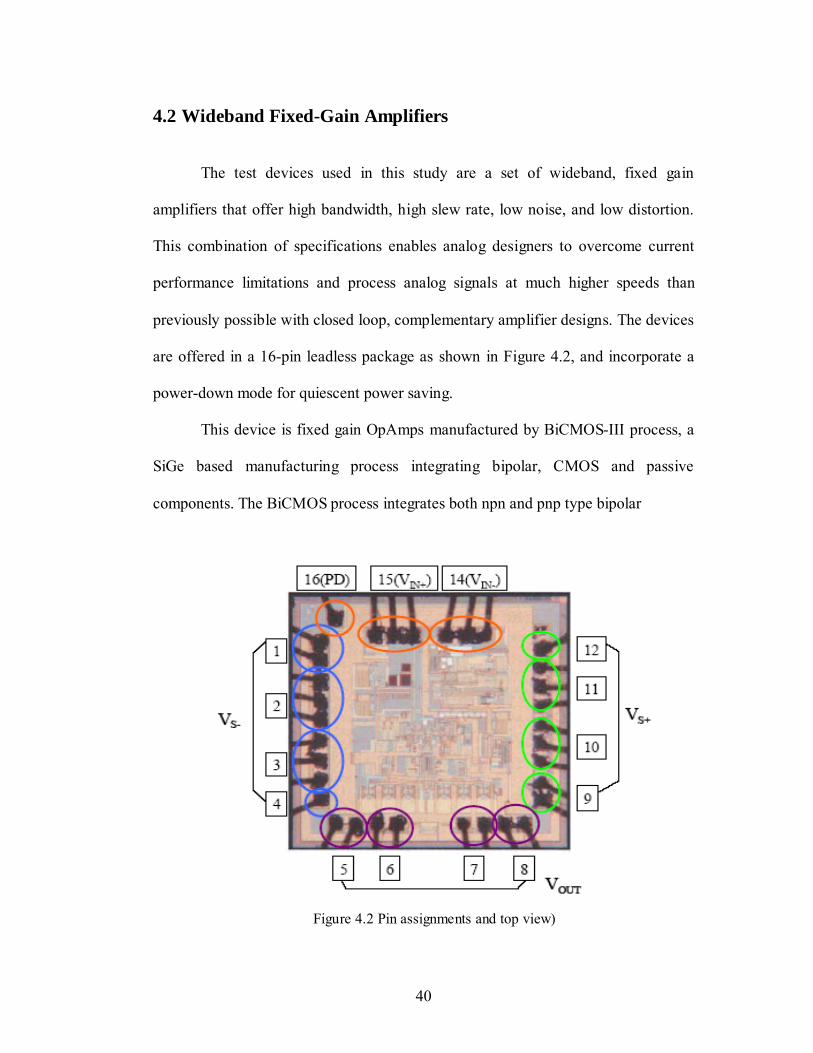
40
4.2 Wideband Fixed-Gain Amplifiers
The test devices used in this study are a set of wideband, fixed gain
amplifiers that offer high bandwidth, high slew rate, low noise, and low distortion.
This combination of specifications enables analog designers to overcome current
performance limitations and process analog signals at much higher speeds than
previously possible with closed loop, complementary amplifier designs. The devices
are offered in a 16-pin leadless package as shown in Figure 4.2, and incorporate a
power-down mode for quiescent power saving.
This device is fixed gain OpAmps manufactured by BiCMOS-III process, a
SiGe based manufacturing process integrating bipolar, CMOS and passive
components. The BiCMOS process integrates both npn and pnp type bipolar
Figure 4.2 Pin assignments and top view)

41
Table 4.2 Features, applications, and device data
Table 4.3 Absolute maximum ratings
Supply Voltage, VS 6V
Input voltage, VI ±VS
Output current, IO 200MA
Maximum junction temperature, TJ 150oC
Operating free-air temperature range, TA -40oC to 85oC
Storage temperature range, Tstg -65oC to 150oC
Lead temperature 1.6 mm (1/16 inch) from case for 10 seconds 300oC
Table 4.4 Recommended operating conditions
Min Max Unit
Dual Supply ±1.5 ±2.5 Supply voltage (VS+ and VS-)
Single Supply 3 5 V
Input common-mode voltage range VS-+1 VS+-1
THS4302 Features Applications for THS4302 Device Data
Fixed Gain Closed Loop Amplifiers
Gain: +5 V/V (14dB)
Wide Bandwidth: 2.4GHz
High Slew Rate: 5500V/µs
High Output Drive: ±180 mA
Power Supply Voltage: +3 V or +5 V
Wideband signal processing Wireless transceivers IF amplifier ADC preamplifier DAC Output buffers Test, Measurement, and instrumentation Medical and Industrial imaging
Die Name: RTHS4302IM Die Size: 53x53 Wafer Fab: TID Assembly site: CAR Pins/Package: 16/RGT Mold compound: SUM EME-7730LF Technology: BiCOM-III 1st metal: TiN/AlCu0.5% 2nd metal: TiN/AlCu0.5% 3rd metal: TiN/AlCu0.5% L/F material: Copper L/F finish: Solder Plate Die Mount: ABL 2600BT Bond Wire: 1.0mil Au, TS

42
transistors, achieving a three times speed increase and upto 50% noise reduction for
OpAmps and other high-performance mixed signal products. This process allows
analog components to operate at 100MHz with a distortion level of 100dB [42].
These parts are COTS (commercial-off-the-shelf) parts. Table 4.2 gives a summary
of various features of OpAmps, applications and device data, and Table 4.3 and
Table 4.4show absolute maximum ratings and recommended operating conditions
for this device.
4.3 ESD test and electrical characterization
The nine test devices were subjected to ESD exposure for the purpose of
evaluation. Test models used for ESD testing were HBM, MM, and CDM. The ESD
test involved “step stress test,” whereby the zapping voltage level is increased by
500 V in HBM and CDM and by 50 V in MM until the components exhibit
electrical malfunctions such as open, short, or parametric shift. In each voltage step,
electrical characteristics are verified and compared with those of the good devices
(test standards from MIL and JEDEC specify 1,000 V in HBM and CDM and 100 V
in MM [18]-[20]).
The devices (sample numbers 11 to 19 were used for ESD testing) were split
into three groups for the three models: three devices for HBM, three devices for
MM, and three devices for CDM. All possible pin connections were used for test pin
connections. The number of discharges was five in each voltage step. The discharge
off interval was 1 second in HBM and MM and 0.5 second in CDM. The discharge
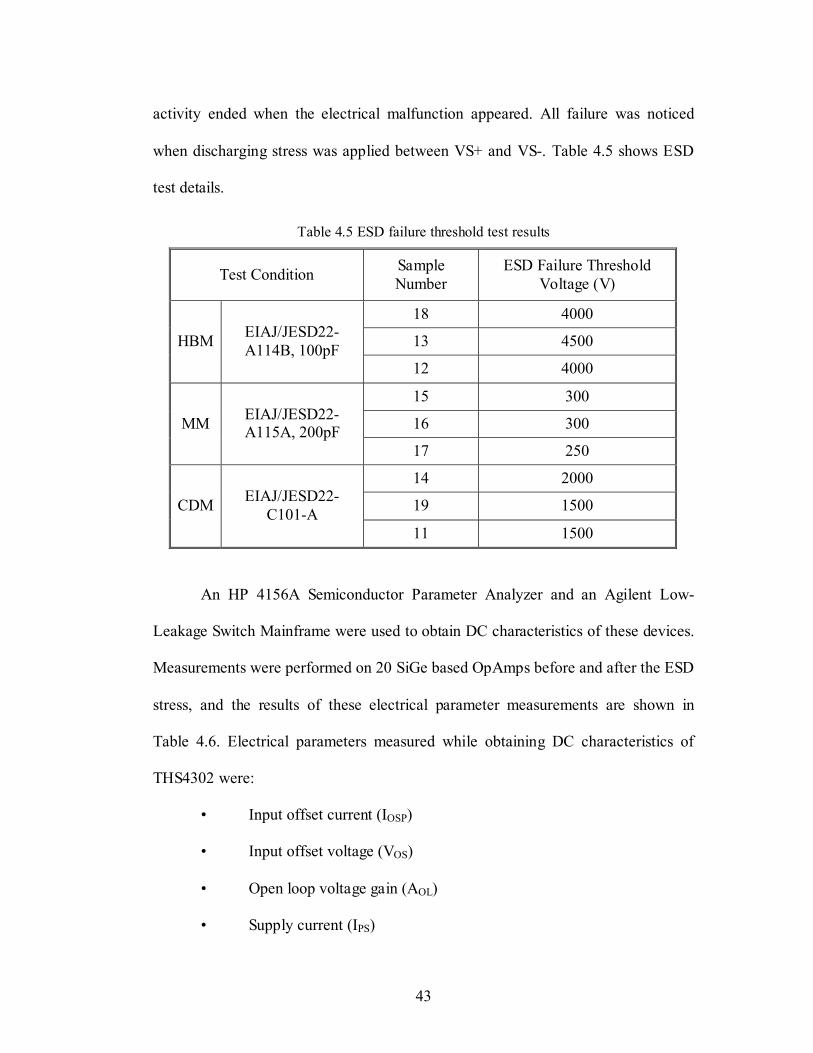
43
activity ended when the electrical malfunction appeared. All failure was noticed
when discharging stress was applied between VS+ and VS-. Table 4.5 shows ESD
test details.
Table 4.5 ESD failure threshold test results
Test Condition Sample Number
ESD Failure Threshold Voltage (V)
18 4000
13 4500 HBM EIAJ/JESD22-A114B, 100pF
12 4000
15 300
16 300 MM EIAJ/JESD22-A115A, 200pF
17 250
14 2000
19 1500 CDM EIAJ/JESD22-C101-A
11 1500
An HP 4156A Semiconductor Parameter Analyzer and an Agilent Low-
Leakage Switch Mainframe were used to obtain DC characteristics of these devices.
Measurements were performed on 20 SiGe based OpAmps before and after the ESD
stress, and the results of these electrical parameter measurements are shown in
Table 4.6. Electrical parameters measured while obtaining DC characteristics of
THS4302 were:
• Input offset current (IOSP)
• Input offset voltage (VOS)
• Open loop voltage gain (AOL)
• Supply current (IPS)

44
The above parameters were measured at two different values of supply
voltage (VS): ±2.5 V and ±1.5 V. The VS+ was applied to the source monitor unit
(SMU3) channel of the parameter analyzer, while VS- was applied to the SMU4
channel of the parameter analyzer (Figure 4.3). The voltage monitor unit (VMU1)
channel was used to measure the output voltage, and the SMU2 channel was used to
apply the negative input voltage (VNEG) to the OpAmp. The SMU1 channel of the
parameter analyzer was connected to ground; therefore, an inverting gain
configuration of the OpAmp was used during the electrical testing. The circuit
shown in Figure 4.3 was used as a test circuit for all measurements in tables and
figures. Figure 4.4 shows a typical DC characteristics of the device with Vs=±2.5 V
before and after ESD stress.
The measurements of electrical parameters (DC characteristics) of sample
numbers 11 to 19 before and after the ESD exposure are shown in Table 4.7 (see
SMU1
SMU2
SMU3
SMU4
VMU1
0.1µF0.1µF
0.1µF0.1µF
+
_
200Ω
SMU1
SMU2
SMU3
SMU4
VMU1
0.1µF0.1µF
0.1µF0.1µF
+
_
200Ω
Figure 4.3 Test setup used for DC characteristics measurements
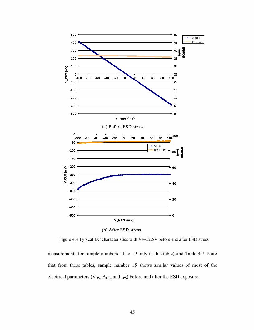
45
measurements for sample numbers 11 to 19 only in this table) and Table 4.7. Note
that from these tables, sample number 15 shows similar values of most of the
electrical parameters (VOS, AOL, and IPS) before and after the ESD exposure.
-500
-400
-300
-200
-100
0
100
200
300
400
500
-100 -80 -60 -40 -20 0 20 40 60 80 100
V_NEG (mV)
V_O
UT
(mV)
0
5
10
15
20
25
30
35
40
45
50
IPSPOS
(mA
)
VOU TIPSPOS
-500
-400
-300
-200
-100
0
100
200
300
400
500
-100 -80 -60 -40 -20 0 20 40 60 80 100
V_NEG (mV)
V_O
UT
(mV)
0
5
10
15
20
25
30
35
40
45
50
IPSPOS
(mA
)
VOU TIPSPOS
-500
-450
-400
-350
-300
-250
-200
-150
-100
-50
0-100 -80 -60 -40 -20 0 20 40 60 80 100
V_NEG (m V)
V_O
UT
(mV)
0
20
40
60
80
100
IPSPO
S (m
A)
VO UTIPSPOS
-500
-450
-400
-350
-300
-250
-200
-150
-100
-50
0-100 -80 -60 -40 -20 0 20 40 60 80 100
V_NEG (m V)
V_O
UT
(mV)
0
20
40
60
80
100
IPSPO
S (m
A)
VO UTIPSPOS
(a) Before ESD stress
(b) After ESD stress
-500
-400
-300
-200
-100
0
100
200
300
400
500
-100 -80 -60 -40 -20 0 20 40 60 80 100
V_NEG (mV)
V_O
UT
(mV)
0
5
10
15
20
25
30
35
40
45
50
IPSPOS
(mA
)
VOU TIPSPOS
-500
-400
-300
-200
-100
0
100
200
300
400
500
-100 -80 -60 -40 -20 0 20 40 60 80 100
V_NEG (mV)
V_O
UT
(mV)
0
5
10
15
20
25
30
35
40
45
50
IPSPOS
(mA
)
VOU TIPSPOS
-500
-450
-400
-350
-300
-250
-200
-150
-100
-50
0-100 -80 -60 -40 -20 0 20 40 60 80 100
V_NEG (m V)
V_O
UT
(mV)
0
20
40
60
80
100
IPSPO
S (m
A)
VO UTIPSPOS
-500
-450
-400
-350
-300
-250
-200
-150
-100
-50
0-100 -80 -60 -40 -20 0 20 40 60 80 100
V_NEG (m V)
V_O
UT
(mV)
0
20
40
60
80
100
IPSPO
S (m
A)
VO UTIPSPOS
(a) Before ESD stress
(b) After ESD stress Figure 4.4 Typical DC characteristics with Vs=±2.5V before and after ESD stress
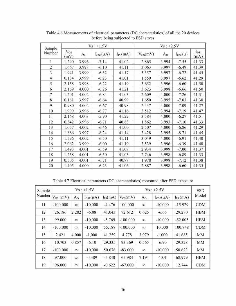
46
Table 4.6 Measurements of electrical parameters (DC characteristics) of all the 20 devices before being subjected to ESD stress
Vs : ±1.5V Vs : ±2.5V Sample Number VOS
(mV) AO IOSP(µA) IPS(mA) VOS(mV) AO IOSP(µ) IPS (mA)
1 1.290 3.996 -7.14 41.02 2.865 3.994 -7.55 41.33 2 1.667 3.998 -6.10 41.11 3.063 3.997 -6.49 41.39 3 1.941 3.999 -6.32 41.17 3.357 3.997 -6.72 41.45 4 0.134 3.999 -6.23 41.01 1.559 3.997 -6.62 41.29 5 2.158 3.998 -6.22 41.19 3.652 3.996 -6.60 41.50 6 2.169 4.000 -6.26 41.21 3.623 3.998 -6.66 41.50 7 1.201 4.002 -6.84 41.03 2.609 4.000 -7.26 41.31 8 0.161 3.997 -6.64 40.99 1.650 3.995 -7.03 41.30 9 0.980 4.002 -6.67 40.98 2.437 4.000 -7.09 41.27
10 1.999 3.996 -6.77 41.16 3.512 3.994 -7.19 41.47 11 2.168 4.003 -5.90 41.22 3.584 4.000 -6.27 41.51 12 0.342 3.996 -6.71 40.83 1.862 3.993 -7.10 41.33 13 1.057 4.002 -6.46 41.00 2.507 4.000 -6.86 41.29 14 1.886 3.997 -8.24 41.14 3.428 3.995 -8.71 41.45 15 1.596 4.002 -6.50 41.11 3.049 4.000 -6.91 41.40 16 2.062 3.999 -6.00 41.19 3.539 3.996 -6.39 41.48 17 1.493 4.001 -6.59 41.08 2.934 3.999 -7.00 41.37 18 1.258 4.001 -6.50 41.03 2.746 3.998 -6.89 41.33 19 0.505 4.001 -6.71 40.88 1.978 3.998 -7.12 41.38 20 1.405 4.000 -6.23 41.06 2.887 3.998 -6.60 41.35
Table 4.7 Electrical parameters (DC characteristics) measured after ESD exposure
Vs : ±1.5V Vs : ±2.5V Sample Number VOS (mV) AO IOSP(µA) IPS(mA) VOS(mV) AO IOSP(µA) IPS (mA)
ESD Model
11 -100.000 ∞ -10,000 -4.476 100.000 ∞ -10,000 -15.929 CDM
12 26.186 2.282 -6.08 41.043 72.612 0.625 -6.66 29.280 HBM
13 99.000 ∞ -10,000 -5.769 -100.000 ∞ -10,000 -52.005 HBM
14 -100.000 ∞ -10,000 55.188 -100.000 ∞ 10,000 100.848 CDM
15 2.421 4.000 -1,000 41.259 4.778 3.979 -1,000 41.685 MM
16 10.703 0.857 -6.10 29.335 93.369 0.565 -6.90 29.328 MM
17 -100.000 ∞ -10,000 50.676 -83.000 ∞ -10,000 50.623 MM
18 97.000 ∞ -0.389 -5.840 65.984 7.194 40.4 68.979 HBM
19 96.000 ∞ -10,000 -0.622 -67.000 ∞ -10,000 12.744 CDM

47
4.4 Failure analysis results
Once ESD testing and electrical characterization were completed, failure
analysis was performed using various identification methods for failure detection
and location. It included visual inspection for anomalies; and X-ray, optical
microscopy, and scanning electron microscopy (SEM) for locating the defect.
Liquid crystal thermal imaging technique and focused ion beam (FIB) microscope
observation were also implemented in order to detect and examine underlying
metallization, diffusion, and passivation layers for failure sites that are not found by
optical microscopy or SEM techniques. Detail failure analysis procedure is shown in
Figure 4.5.
Failure analysis procedures aim to identify the failure mode and failure
Destructive Physical Analysis
Internal Microscopic Examination - O/M, SEMVisible Failure Modes
Documentation of Findings(Photos Responses) Remove Metallization : Etching
Microscopic Exam. : O/M, SEM
Photo-Emissionor Liquid Crystal
Failure Mechanism Identification
Non-Visible Failure Modes
SEM Analysis O/M
ESD Simulation for good devices
Non-destructive analysis
Figure 4.5 Failure analysis procedure

48
location, and establish a physical signature associated with electrical failure of the
devices. Once all experimental devices had been functionally tested, the devices
failing the electrical testing acceptance criteria were subjected to failure analysis.
The failing devices were then decapsulated and examined using optical microscopy,
scanning electron microscopy and FIB techniques. Each device’s failure location
and signature were identified and documented for each ESD test model.
When the failure could not be located easily on the surface of the die, circuit
analysis and failure isolation techniques were required. In this study, thermal
imaging technique using liquid crystal was used to find the location of the failures.
Once the failure location was identified, subsurface analysis was required to further
reveal the damage location. A deprocessing technique was employed using reactive
ion etching (RIE) to remove the passivation layers and intermetallic dielectric
material. This also includes sub-micron cross-sectioning using focused ion beam
techniques.
Liquid Crystal Thermal Imaging Analysis
Liquid crystal thermal analysis for use on a decapsulated device is
considered to be a good technique for locating failure sites, especially for ESD
stressed devices. The test setup is shown in Figure 4.6. This process is capable of
detecting the abrupt temperature change on the die surface. In this process, first
liquid crystal was applied on the die surface of the decapsulated device, and input
voltage was directly applied to the device through the bond pads and test needles
that were connected to the DC power supply.

49
Figure 4.6 Test set-up for liquid crystal thermal imaging analysis
Figure 4.7 Liquid crystal analysis result for a good device
(b) After input voltage applied (a) Before input voltage applied

50
This was specified in device specifications in order to duplicate actual
electrical operating conditions. During the analysis, the die surface of the devices
was continuously monitored using optical microscopy to detect the transient
temperature profile. The results are shown in Figure 4.7 and Figure 4.8. In the case
of good devices (Figure 4.7), once input voltage is applied to the device, the
temperature of whole die almost uniformly goes up, which implies there is no
specific area on the die surface that generates excessive heat. However, in the case
of a failed device (Figure 4.8), the area of failure location on the die surface
generates excessive heat, and this can be detected as a color change of the liquid
crystal using optical microscopy. In Figure 4.8, the arrow indicates a certain region
that generates an abnormal amount of heat, and therefore further detailed failure
analysis should be focused on this region. Further analysis using focused ion beam
(FIB) and environmental scanning electron microscopy (E-SEM) to find exact
failure location will be described in the next section of this chapter.
Figure 4.8 Liquid crystal analysis result for failed devices
(a) Before input voltage applied (b) After input voltage applied
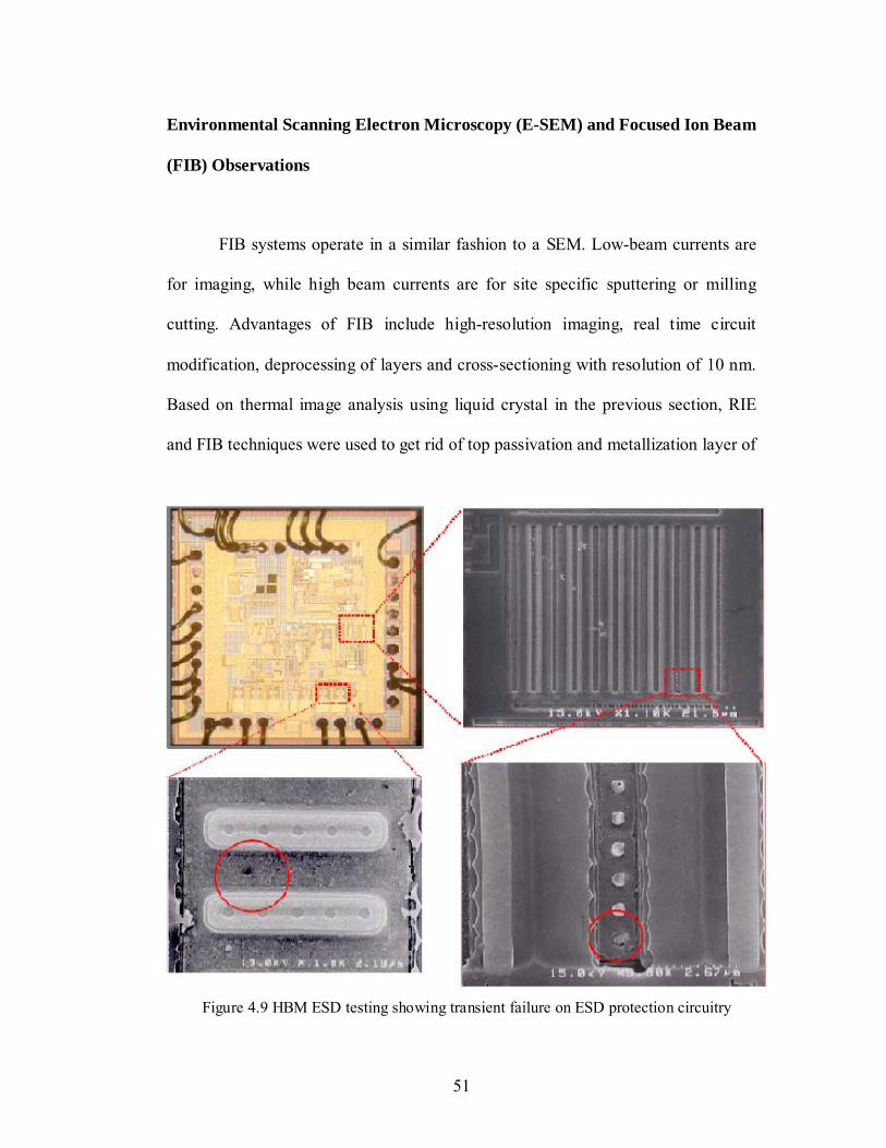
51
Environmental Scanning Electron Microscopy (E-SEM) and Focused Ion Beam
(FIB) Observations
FIB systems operate in a similar fashion to a SEM. Low-beam currents are
for imaging, while high beam currents are for site specific sputtering or milling
cutting. Advantages of FIB include high-resolution imaging, real time circuit
modification, deprocessing of layers and cross-sectioning with resolution of 10 nm.
Based on thermal image analysis using liquid crystal in the previous section, RIE
and FIB techniques were used to get rid of top passivation and metallization layer of
Figure 4.9 HBM ESD testing showing transient failure on ESD protection circuitry

52
the devices. Figure 4.9 shows the failure sites for HBM stressed devices observed
using E-SEM, after deprocessing the layers of die with RIE and FIB. The sizes of
defects were observed to be much smaller than 1 mm. The failure location was the
ESD protection transistor area for positive power supply voltage pins and contact
spiking failure was also observed in the ESD protection diode for positive power
supply voltage pins.
The same deprocessing and observation were performed for MM and CDM
ESD stressed devices. The results are shown in Figure 4.10 and Figure 4.11. In the
case of MM stressed device (Figure 4.10) failure location and signature were
Figure 4.10 MM ESD testing showing transient failure on ESD protection circuitry
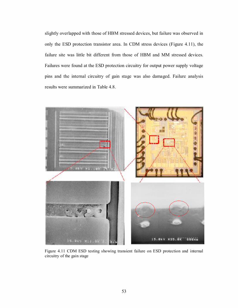
53
slightly overlapped with those of HBM stressed devices, but failure was observed in
only the ESD protection transistor area. In CDM stress devices (Figure 4.11), the
failure site was little bit different from those of HBM and MM stressed devices.
Failures were found at the ESD protection circuitry for output power supply voltage
pins and the internal circuitry of gain stage was also damaged. Failure analysis
results were summarized in Table 4.8.
Figure 4.11 CDM ESD testing showing transient failure on ESD protection and internal circuitry of the gain stage

54
Table 4.8 Characteristics of failure signatures
ESD test models
HBM MM CDM
Failure mode Electrical malfunction (resistive short between power supply pins)
Failure location
ESD protection transistor and diode area for input power supply voltage pins
Only ESD protection transistor area for input power supply voltage pins
ESD protection transistor area for output power supply voltage pins and gain stage of internal circuitry
Failure signature Junction burnout, gate oxide damage, contact spiking
Junction burnout, gate oxide damage
Junction burnout, gate oxide damage
4.5 Discussions and conclusions
The evaluation tests for the ESD failures show the main failure modes were
electrical malfunction and parametric shifts in device characteristics. The current/
voltage relationship before and after the ESD stress shows short circuit type failure
between supply voltage pins (VS+/VS-, positive and negative supply voltage pin).
Even though an identical level of ESD voltage was applied to all the possible pin
connections, no electrical degradation was found from the current voltage curve of
other pin connections in ESD stressed devices. This indicates that the supply voltage
pins are most sensitive to the ESD stress in this device, regardless of the type of
applied ESD test models.
The failure signatures and locations slightly overlap between HBM and MM
stressed devices. The failures from both test models show the failure on the ESD
55
protection circuitry for input supply voltage pins. But three different ESD test
models produced somewhat different failure locations and signatures on the same
device. After decapsulation and deprocessing by using reactive ion etching (RIE),
the physical failures could be seen as pits or melted junction failures. In terms of the
location, all failures resulting from HBM occurred in the protection transistor region
between supply voltage pins and no failure signature was found in the input and
output stages of the internal circuitry. In the case of MM ESD stress, similar but
little bit more severe failure happens same transistor area. But unlike HBM stress no
failure was observed in diode area. Failure occurs in only ESD protection transistor
area. On the other hand, CDM ESD stress caused damage both in the supply voltage
protection circuitry and internal gain stage of the circuitry. CDM stressed devices
showed more severe and localized catastrophic failure in different regions, as
compared to those in the case of HBM and MM stressed devices.
Through ESD failure threshold test and failure analysis, I showed different
ESD test models caused different failure location and signatures. This difference can
be explained like this. ESD protection elements are triggered by transient input
voltage or current depending on the type of protection structures and all protection
circuitry has their own triggering times. Usually, transistor protection circuit has
faster triggering time than diode and different ESD pulses have different speed,
which means different pulse duration. HBM pulse has around 10 ns rise time MM
pulse has 5 ns rise time. CDM has much faster so, it has less than 1ns.
The comparatively slow HBM pulse has been detected by both of ESD
protection diode and transistor, so both protection circuits failed. But in case of little

56
bit faster MM pulse, it is not detected by protection diode; it is only detected by
protection transistor. But much faster CDM pulse goes into the internal circuitry
without triggering both of protection circuitry.
So it shows that different speed of different ESD models caused different
failure location and signatures in the same devices and it is due to the different pulse
duration of the different ESD test models. This phenomenon needs to be considered
for the protection circuit design and root cause analysis for field failures.
Figure 4.12 ESD paths through the internal circuit
In general, HBM-like events tend to damage the protection circuit (input
buffer), while the majority of CDM failures tend to occur beyond the protection
circuit, which is partly due to the nature of CDM. Due to the rapid sub-nanosecond
rise time (usually less than 0.5 ns), protection devices may not be able to turn-on
57
and clamp the discharge voltage to a safe level before internal circuitry is damaged.
So, the ESD protection circuit for this particular device is not effective for CDM
ESD stress or CDM-like rapid electrical stress. Figure 4.12 shows ESD protection
circuitry and their locations for this device.
All ESD failure showed multiple damage sites on the device. A possible
explanation for this effect is that undetectable damage was generated before the
ESD voltage level went up to the hard threshold voltage, where the catastrophic
failure of the device occurred.
SiGe OpAmps, which are based on the BiCOM technology, were subjected
to ESD testing and failure analysis. This study demonstrates the potential of
physical failure analysis to reveal the subtle ESD failure location and signatures, as
it is very difficult to distinguish failures from failure mode and electrical
characteristic data of each ESD test model. The findings of this study are;
• The failure mode of all ESD stressed devices was electrical parametric
degradation caused by short circuits.
• Supply voltage pins are most sensitive to the ESD stress in this device,
regardless of the type of applied ESD test models.
• Based on physical failure analysis, failure locations match with protection
circuitry between power supply pins.
• HBM and MM stressed devices show different location and signature in the
same supply voltage protection circuitry.
• CDM stress causes damage in both supply voltage protection circuitry and
internal gain stage of the circuitry.
58
• All types of ESD test models caused multiple damage signatures on the devices.

59
5. INVESTIGATION OF FIELD FAILURES AND
FAILURES CAUSED BY EOS AND ESD IN GAAS
MMIC
In this chapter, the results of failure mode and effect analysis, visual
inspection, electrical test, X-ray inspection, optical microscopy and scanning
electron microscopy analysis are presented on failed GaAs MMIC voltage variable
absorptive attenuators. Human body model (HBM) and machine model (MM)
electrostatic discharge tests and electrical overstress test were performed to replicate
the failure and correlated with each other. ESD and EOS tested and field failed
devices have shown distinctive failure characteristics such as damage sites and
severity in accordance with controlled test conditions.
5.1 GaAs devices and ESD
As the high speed wired communication, wireless network, high-speed test
equipment, and magnetic recording industries are growing rapidly, advanced
semiconductors, such as gallium arsenide (GaAs), indium Phosphide and silicon
germanium carbon technologies are playing a more significant role. GaAs
monolithic microwave ICs (MMICs) are integrated structures, which contain planar
transmission lines, distributed elements, and active devices on the same substrate.
Unlike silicon-based technology, GaAs substrates have no dielectric oxide layer due
to their semi-insulating nature and gold or gold-based alloys, such as AuGeNi are

60
materials for metallization on the device [43]. So, it is not practical to build
MOSFETs on GaAs substrates. Hence the MESFET is the most common active
device in the GaAs IC industry. MMICs are commonly used in telecommunication
products, TV receivers for satellite broadcasting, and in radar and navigation
systems.
A number of publications have addressed the ESD sensitivity of GaAs
devices and they are more sensitive to ESD than silicon devices [44]-[46]. GaAs is
gaining acceptance as another standard material for IC devices, because the high
electron mobility compared to silicon enhances the performance of the device [47]
and is more applicable to high performance devices. However, GaAs devices have
lower thermal conductivity than silicon and ESD/EOS damage appears from
semiconductor melting caused by localized overheating. So, ESD robustness of
devices is a strong function of the material melting temperature, and thermal
conductivity [48]. Due to the low thermal conductivity and low melting temperature
of GaAs, GaAs devices are more sensitive to ESD than Si or SiGe devices. The low
conductivity of GaAs devices may impose additional thermal considerations. But
ESD robustness depends on feature size, process maturity and other parameters (not
only material properties). Additionally, the temperature dependence of material
properties needs to be considered to explain ESD characteristics. For example, the
thermal conductivity of GaAs is less than half of Si and it decreases with
temperature approximately to –1.29 power (silicon changes at about the –1 power).
This relationship implies that if circuits with identical power densities were

61
constructed from GaAs and Si, the GaAs device would get hotter than Si and the
generated heat can be easily concentrated in a smaller region.
5.2 Experimental approach
Controlled failure production through simulation could be the easiest way to
quantify root causes of failure due to ESD. In this study, a commercially available
simulator will be used to create HBM, MM, and CDM ESD damages. The testing
approach will attempt to reproduce the damage of ESD failure and quantify the
Visual Inspection
Non-Destructive Test
Establish Potential Failure Modes / Mechanisms
ESD Simulation with Known Good Device
FMEA Evaluation
Root CauseIdentified?
yes
no
Protection Method Development
Establish Assessment and Test Plan to Identify CausesRoot Cause
Analysis
Effectiveness Assessment of ESD Test Models
Correlationwith Actual Field FailureFailure Site/Signature Identification
Find Failure Mechanism
Destructive Physical Analysis
Figure 5.1 Flowchart of failure analysis process
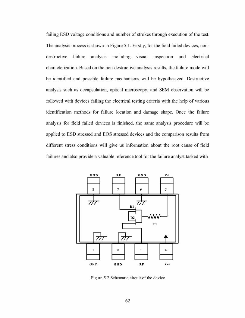
62
failing ESD voltage conditions and number of strokes through execution of the test.
The analysis process is shown in Figure 5.1. Firstly, for the field failed devices, non-
destructive failure analysis including visual inspection and electrical
characterization. Based on the non-destructive analysis results, the failure mode will
be identified and possible failure mechanisms will be hypothesized. Destructive
analysis such as decapsulation, optical microscopy, and SEM observation will be
followed with devices failing the electrical testing criteria with the help of various
identification methods for failure location and damage shape. Once the failure
analysis for field failed devices is finished, the same analysis procedure will be
applied to ESD stressed and EOS stressed devices and the comparison results from
different stress conditions will give us information about the root cause of field
failures and also provide a valuable reference tool for the failure analyst tasked with
1 2 3 4
8 7 6 5
V ccR FG N DG N D
G N D R F G N D V c
R 1
1 2 3 4
8 7 6 5
1 2 3 4
8 7 6 5
V ccR FG N DG N D
G N D R F G N D V c
R 1
D1
D2
1 2 3 4
8 7 6 5
V ccR FG N DG N D
G N D R F G N D V c
R 1
1 2 3 4
8 7 6 5
1 2 3 4
8 7 6 5
V ccR FG N DG N D
G N D R F G N D V c
R 1
D1
D2
Figure 5.2 Schematic circuit of the device

63
a transient event resulting in ESD and EOS failures.
The test device used for this study is an AT-110, a voltage absorptive
attenuator manufactured by MACOM based on GaAs MMIC technology. The
schematic circuit of this device is shown in Figure 5.2.
In order to insure proper simulation and repeatable ESD results, simulator
waveform performance will be verified with standard procedures outlined in the
ESD Association EIAJ/JEDEC 22-A114B HBM and A115A MM ESD
specifications and C101A CDM ESD specification. HBM simulation was performed
with three GaAs MMICs in a preliminary study. The devices had no power applied
during ESD testing. The result of the analysis was documented and kept in a
database. In this study, not only HBM but also MM and CDM were simulated in
accordance with different peak voltages and numbers of application. The
combination of these models and continuous model applications are also interested
for further analysis.
In order to analyze the failures associated with EOS, four unused (good)
devices were subjected to a DC voltage applied between Vcc and ground pin and Vc
and ground pins. Electrical characteristics of the devices were analyzed by I-V
curve tracer after EOS test. The test voltage was increased in steps 1 V, until the test
devices exhibit electrical malfunctions. No other power was supplied to devices
during EOS test and all other pins were floating.
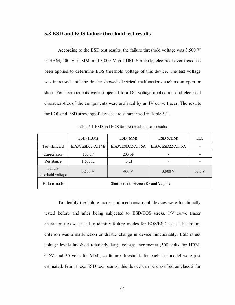
64
5.3 ESD and EOS failure threshold test results
According to the ESD test results, the failure threshold voltage was 3,500 V
in HBM, 400 V in MM, and 3,000 V in CDM. Similarly, electrical overstress has
been applied to determine EOS threshold voltage of this device. The test voltage
was increased until the device showed electrical malfunctions such as an open or
short. Four components were subjected to a DC voltage application and electrical
characteristics of the components were analyzed by an IV curve tracer. The results
for EOS and ESD stressing of devices are summarized in Table 5.1.
Table 5.1 ESD and EOS failure threshold test results
To identify the failure modes and mechanisms, all devices were functionally
tested before and after being subjected to ESD/EOS stress. I/V curve tracer
characteristics was used to identify failure modes for EOS/ESD tests. The failure
criterion was a malfunction or drastic change in device functionality. ESD stress
voltage levels involved relatively large voltage increments (500 volts for HBM,
CDM and 50 volts for MM), so failure thresholds for each test model were just
estimated. From these ESD test results, this device can be classified as class 2 for
400 V
0 Ω
200 pF
EIAJ/JESD22-A115A
ESD (MM)
Short circuit between RF and Vc pinsFailure mode
37.5 V3,000 V3,500 VFailure
threshold voltage
--1,500 ΩResistance
--100 pFCapacitance
-EIAJ/JESD22-A115AEIAJ/JESD22-A114BTest standard
EOSESD (CDM)ESD (HBM)
400 V
0 Ω
200 pF
EIAJ/JESD22-A115A
ESD (MM)
Short circuit between RF and Vc pinsFailure mode
37.5 V3,000 V3,500 VFailure
threshold voltage
--1,500 ΩResistance
--100 pFCapacitance
-EIAJ/JESD22-A115AEIAJ/JESD22-A114BTest standard
EOSESD (CDM)ESD (HBM)
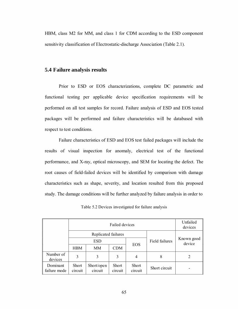
65
HBM, class M2 for MM, and class 1 for CDM according to the ESD component
sensitivity classification of Electrostatic-discharge Association (Table 2.1).
5.4 Failure analysis results
Prior to ESD or EOS characterizations, complete DC parametric and
functional testing per applicable device specification requirements will be
performed on all test samples for record. Failure analysis of ESD and EOS tested
packages will be performed and failure characteristics will be databased with
respect to test conditions.
Failure characteristics of ESD and EOS test failed packages will include the
results of visual inspection for anomaly, electrical test of the functional
performance, and X-ray, optical microscopy, and SEM for locating the defect. The
root causes of field-failed devices will be identified by comparison with damage
characteristics such as shape, severity, and location resulted from this proposed
study. The damage conditions will be further analyzed by failure analysis in order to
Table 5.2 Devices investigated for failure analysis
Failed devices Unfailed devices
Replicated failures ESD
HBM MM CDM EOS
Field failures Known good device
Number of devices 3 3 3 4 8 2
Dominant failure mode
Short circuit
Short/open circuit
Short circuit
Short circuit Short circuit -

66
find from where the damage causes are created and provide the methodology to
protect. Total 21 devices were subjected to failure analysis. It includes 11 ESD
stressed devices, 4 EOS stressed devices, 8 burn in-screen failed devices and 2
known good devices Table 5.2.
5.4.1. Failure mode identifications
The analysis involves running a DC analysis on each failed IC to check for
shorts and opens at the each terminal with I-V curve tracer. With ESD tested GaAs
MMIC, the path from RFin to RFout goes through the gate diodes in FET. A short
of either diode D1 or D2 produces an abnormal curve shape. The path from Vc to
RFin or RFout goes through either diode D1 or D2 and resistance R1. A short across
Figure 5.3 Failure mode identifications
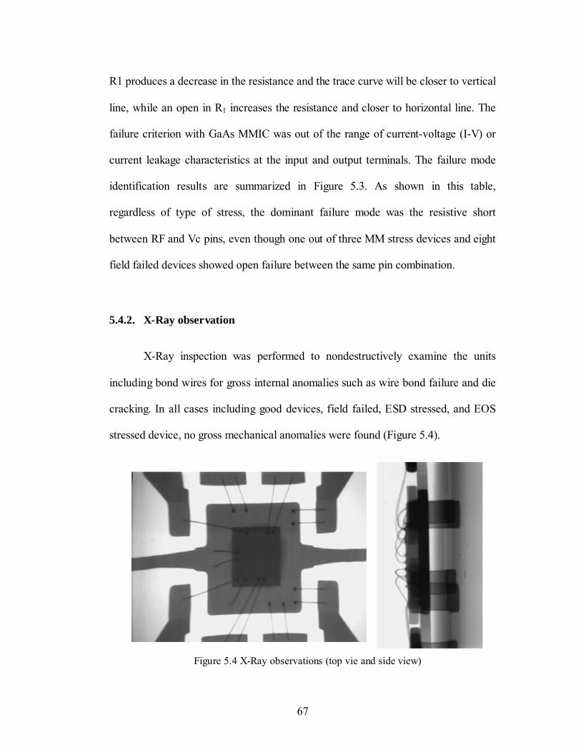
67
R1 produces a decrease in the resistance and the trace curve will be closer to vertical
line, while an open in R1 increases the resistance and closer to horizontal line. The
failure criterion with GaAs MMIC was out of the range of current-voltage (I-V) or
current leakage characteristics at the input and output terminals. The failure mode
identification results are summarized in Figure 5.3. As shown in this table,
regardless of type of stress, the dominant failure mode was the resistive short
between RF and Vc pins, even though one out of three MM stress devices and eight
field failed devices showed open failure between the same pin combination.
5.4.2. X-Ray observation
X-Ray inspection was performed to nondestructively examine the units
including bond wires for gross internal anomalies such as wire bond failure and die
cracking. In all cases including good devices, field failed, ESD stressed, and EOS
stressed device, no gross mechanical anomalies were found (Figure 5.4).
Figure 5.4 X-Ray observations (top vie and side view)

68
5.4.3. Decapsulation and optical microscopy/ESEM observations
Internal visual inspection of the die and bond wires was carried out at
various magnifications. A device with normal characteristics was also decapsulated
for visual comparison. HBM ESD stressed devices show anomalies near the RFout
pin, which leads for electrical short between RFout and Vc pins. In Figure 5.5, arrow
indicates electrical damage located in the gate channel regions of the devices. The
size of damage was as small as a few micro-meters and multiple damage spots were
found in the same device. As shown in Figure 5.6, larger molten damage was also
found in the same device.
CDM and MM stressed device shows similar failure signature with those of
HBM stressed devices. Figure 5.7 shows drain junction edge failure in MM stressed
devices and Figure 5.8 shows a molten failure of the internal FET junction region
Figure 5.5 HBM-stressed device

69
Figure 5.6 HBM-stressed device
Figure 5.7 MM-stressed device
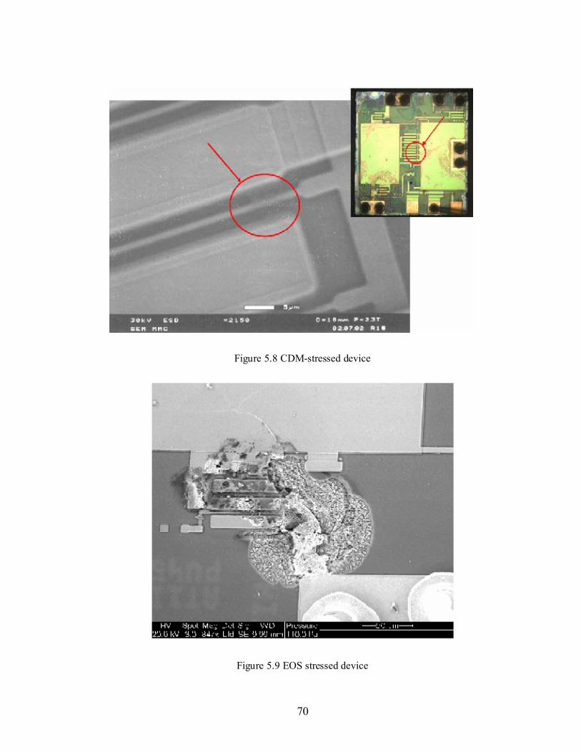
70
Figure 5.8 CDM-stressed device
Figure 5.9 EOS stressed device

71
Figure 5.10 Field failed device
Figure 5.11 Field failed device showing the failure in the resistor area and a mechanical crack in the capacitor area

72
resulting from CDM ESD stress. Like HBM stressed devices, multiple damage spots
were found in the same device, but the failure size was always smaller than a few
micro meters. Damage resulting from HBM and CDM ESD stress caused an
electrical short circuit and appears to be very typical damage due to ESD events.
This surface breakdown can occur when the voltage is high enough to bridge a gap
between metallization or junctions, which is called a gaseous arc breakdown.
Failures due to EOS were located on the die surface bond pad area and
damage was comparatively large (100 µm~) and single damage spots. Figure 5.9
shows the electrical short located near a gate channel of the device. In addition,
damage was located at the RF input resistor area.
In the case of field failed devices, the failure signature was very similar to
those of HBM and CDM stressed devices Figure 5.10 show junction burnout failure
of the input FET region. But the same device of field failure shows the damage of
input resistor and capacitor area, which is different from any ESD stressed device or
EOS stressed device. Figure 5.11 shows a mechanical crack in the capacitor area
and a molten anomaly in input resistor area.
5.5 Summary and conclusions
In this chapter, the damage caused by EOS and ESD was investigated
through EOS and ESD simulation tests and failure analysis. The failure modes and
signature were documented and photographed. In addition, EOS and ESD sensitivity

73
of the device was determined. The summary of the analysis results is shown in
Table 5.3.
The analysis of the failed device from the field, EOS and different ESD test
models revealed different failure locations and signature, even though they showed
exactly the same failure mode, which implies the failure mode by itself does not
provide enough information about the root cause. The study of EOS/ESD combined
stress and differentiating the subtle difference between damage due to the several
distinct ESD models should be performed to determine the root cause of field
failures.
Table 5.3 Characteristics of failure signatures
HBM ESD MM ESD CDM ESD EOS Field failure
Failure mode Resistive short between RF input FET
Failure location
gate junction area of
input FET
drain edge of
FET region
gate junction area of FET
Input resistor and
metallization close to bond
pad
gate junction area of input FET, Input/output resistor and capacitor
Failure signature
Junction burnout
Junction burnout
Junction burnout
Die burnout Metallization burnout Mechanical crack
Junction burnout, Mechanical crack
Failure size ~ 5 µm ~3 µm Around 100
µm ~5 µm, ~ 100 µm
HBM stressed devices show the damage in a gate channel of the FET and
CDM stressed devices show similar failure signature to those of HBM stressed
devices. Failures due to EOS are located on the die surface around the input pins

74
and damages are comparatively large (100 µm~) and single damage spots. So they
can be easily detected even at a low magnification observation. An important
difference between ESD and EOS damage was the size of the damaged site due to
the energy and pulse difference induced. Another difference was that damaged
devices from ESD stress showed multiple discharge damage spot, while EOS
showed single damage spot.
HBM stressed devices exhibit the damage in the gate channel of the FET. On
the other hand, CDM stressed devices show similar failure signature to those of
HBM stressed devices which is not consistent with the failure analysis result for
silicon device. In silicon devices, CDM is known to cause oxide breakdown damage
and HBM stress causes the junction damage which is a key difference of the failure
signature from HBM and CDM ESD stress. But in this case of GaAs MESFET,
there is no thin oxide that is vulnerable to CDM ESD stress, CDM type stress also
causes similar damage to that of HBM stress which makes root cause analysis more
confused in case of MESFET devices. This is also consistent with ESD failure
threshold voltage level in this case. In silicon devices, CDM ESD failure threshold
voltage is much lower than that of HBM ESD stress. But in this case, it is close to
HBM failure threshold level. (3500V in HBM 3000 V in CDM)
These analysis data can be used in replicating the actual field failures. Field
failed devices show similar signature to those of HBM stressed devices in terms of
failure location and size, but they do not exactly match with each other. Field failed
devices also showed electrical transient damage in the input resistor area and
mechanical cracks in the capacitor area, which are not observed in HBM ESD

75
stressed device. In order to find the root cause of the field failures, further analysis
needs to be performed. This will be described in the next chapter (Chapter 6).
In this chapter, the failure modes and signatures of ESD and EOS tested
samples were classified, documented, and photographed after failure analysis. They
were referenced to find root causes of field failed components by comparison. The
importance of the comparison process is to identify damage causing process
conditions that components can experience and to provide a process guideline and a
component and system level design strategies for ESD/EOS protection.

76
6. ESD-INDUCED LATENT FAILURES
This chapter describes the investigation of ESD susceptibility and latent
damage effect on GaAs MESFET devices. Electrical degradation due to ESD-
induced latent damage in GaAs MESFET devices after cumulative low-level ESD
stress is also studied.
ESD causes latent failures if the device is repeatedly stressed under low ESD
voltage conditions. Depending on the stress level, ESD voltage can cause other
premature damage leading eventually to component failures. Using detailed failure
analysis, combined with electrical characterization, the failure modes and signatures
of EOS stressed devices with/without initial low-level ESD stress were compared
and documented. A stress hardening effect on ESD susceptibility, partial alleviation
of cumulative effect of repeated ESD discharges by thermal annealing and the latent
failure mechanisms particularly for GaAs devices was also discussed in this chapter.
6.1 ESD Latent failure
ESD can cause catastrophic failure and latent failure as well. The threshold
of failure is determined by the magnitude of maximum voltage that a device can
absorb without permanent damage. Dielectric failure and thermal failure are
generally considered to be catastrophic failures because these failures cause
permanent electrical malfunction or degradation. However, it is also possible for
physical damage to be produced below this threshold voltage without degradation of

77
device functionality. ESD latent failure is a time-dependent malfunction that occurs
under use conditions as a result of earlier exposure to electrostatic discharge that
does not result in an immediately detectable problem [49], whereby a semiconductor
component stressed below its ESD threshold fails prematurely during normal
operation [50]. The existence of latent ESD damages in IC devices has been
addressed by several researchers, but latent failure still remains controversial. Some
researchers believe that while latency effects may be possible, they occur only with
a very low probability. Other researchers reported evidence to support the presence
of latent damages. Furthermore, as for compound semiconductor such as GaAs
devices, some researches reported that unlike silicon MOSFETs, GaAs MESFETs
have no gate oxide which is vulnerable to latent damage, so MESFETs and
MESFET-based ICs show no cumulative or long term effects from ESD pulses
applied below levels which cause instantaneous damages [51]. So far, there has not
been a clear quantification of the latent damage, nor has there been a correlation
established between the possible leakage current induced by latent ESD damage and
eventual failure.
In order to get a better understanding of latent failure phenomena in non-
silicon devices, in this study the ESD susceptibility and latent effect of GaAs will be
investigated to quantify damages due to ESD stress. GaAs MESFET devices were
subjected to various types of ESD stress; various test models (HBM, MM and
CDM) and various stress type (single stress and multiple stress). And during the
multiple ESD stress to the devices, a series of measurements including the backward
leakage current measurement were performed to monitor latent failures on

78
commercially available GaAs devices. To investigate latent effect on devices
reliability and lifetime, after the ESD tests, assessment of device reliability
including EOS test will be performed. Additionally, stress weakening and hardening
effect due to prior low-level ESD stress will be also discussed. The relationship
between ESD-related latent failure and EOS robustness of devices has not been
reported.
This part of study shows that ESD can cause catastrophic failures and also
cause the failures under the normal operating conditions. Additionally, this study
reports that ESD voltage lower than hard failure voltage can cause other damage
even though there is no electrical degradation of devices and no degradation of the
device in terms of ESD robustness.
6.2 GaAs Devices and Latent Failure
The topic of latent failure in the low ESD voltage condition has been and
continues to be a controversial subject. Many previous researches have reported
latency and the evidence that latent failures exist [52]-[54]. But in terms of latent
failure mechanism resulting from ESD, most of previous researches are focusing on
the gate oxide as a source of latency. Due to this reason, it has been believed that
damage from ESD is always catastrophic in GaAs devices even though it is
generally known that GaAs MESFETs have a low susceptibility to ESD. Rubalcave
and Roesch [55] did a study of the latent failure of GaAs MESFET devices and
circuits. This paper demonstrated that GaAs ICs have no latent or cumulative effects
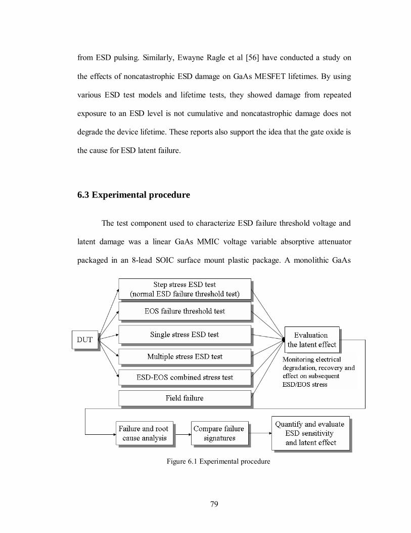
79
from ESD pulsing. Similarly, Ewayne Ragle et al [56] have conducted a study on
the effects of noncatastrophic ESD damage on GaAs MESFET lifetimes. By using
various ESD test models and lifetime tests, they showed damage from repeated
exposure to an ESD level is not cumulative and noncatastrophic damage does not
degrade the device lifetime. These reports also support the idea that the gate oxide is
the cause for ESD latent failure.
6.3 Experimental procedure
The test component used to characterize ESD failure threshold voltage and
latent damage was a linear GaAs MMIC voltage variable absorptive attenuator
packaged in an 8-lead SOIC surface mount plastic package. A monolithic GaAs
Figure 6.1 Experimental procedure

80
MMIC uses a mature 1 micron process and the device functional schematic is
illustrated in Figure 5.2 in chapter 5. All the electrical testing was performed at
room temperature. To investigate both cumulative and latent damage effects on the
ESD threshold voltage, several test methods including commercial test standards
(JEDEC, MIL-STD) have been proposed as follows and illustrated in Figure 6.1.
Three types of test using both positive and negative current discharge will be
performed on each new device.
1. Single-stress test: the purpose of this test is to determine the voltage level at
which a single pulse caused failure. The package pin under the test is subjected
to a single pulse starting at a specific low-level voltage. The test is repeated with
new devices until failure occurred after a single pulse
2. Step-stress test: the purpose of this test is to investigate whether the failure
threshold voltage is dependent on the previous applied voltage. The pin under
test is subjected to step stress starting at a specific low voltage level, and the
voltage is increased in equal increments as specified in test standards until
failures occur.
3. Multiple stress test: this test is performed to determine the typical voltage level
at which approximately 30 to 50 pulses are required to produce a significant
change in the electrical characteristics.
In the multiple stress tests, the test devices were initially subjected to ESD
stress at amplitudes less than the actual failure threshold voltage and the additional

81
level of ESD stress upto actual failure threshold voltage was applied to degraded
devices. After the tests, the failure threshold voltages obtained in each test were
compared with each other. The ESD latent damaged devices were then evaluated for
other reliability problem using an EOS or ESD threshold test. Higher voltage was
intentionally applied to the test devices through the input voltage pin until devices
showed an electrical malfunction and then those results were compared with the
result of controlled devices which are not pre-ESD stressed. Also, human body
model (HBM) and machine model (MM) ESD test were conducted. Since there is
no standard test method for the EOS test, a specific overvoltage was applied until
the devices showed electrical malfunction.
The ESD tests were performed using a commercially available ESD
simulator, Electro-tech system model 910. This simulator includes an RLC circuit
module to incorporate separate parallel paths for human body and machine model
discharges, to replicate actual ESD pulse conditions. The pin-under-test was
subjected to two types of HBM and MM tests and both positive and negative
polarity pulses. After all the tests were conducted, all the failed devices were
subjected to physical failure analysis, and failure mode, location and signature have
been compared with each other. Additionally the characteristics of failures are also
correlated with field failures described in the previous chapter (chapter 5).

82
6.4 Test Results
6.4.1. ESD/EOS failure threshold test results
First of all, to induce latent damage in the test devices and determine the
ESD hard failure threshold, generally accepted ESD test threshold tests have been
performed and then we determined proper stress level to induce ESD latent failure
on our test devices. Two primary test methods, human body model (HBM) and
machine model (MM) were used.
According to the ESD test results, failure threshold voltage was 3,500 V in
HBM and 400 V in MM. Similarly, electrical overstress has been applied to
determine the EOS threshold voltage of this device. The test voltage was increased
until the device showed electrical malfunctions such as open or short. Four
components were subjected to a DC voltage application and electrical characteristics
of the components were analyzed by I-V curve tracer. The results for EOS and ESD
Table 6.1 ESD and EOS failure threshold test result
ESD (HBM) ESD (MM) EOS
Test standard EIAJ/JESD22-A114B
EIAJ/JESD22-A115A -
Capacitance 100 pF 200 pF -
Resistance 1500 Ω 0 Ω -
Failure threshold voltage 3,500 V 400 V 37.5 V
Failure mode Short circuit between RF and Vc
Short circuit between RF and Vc
Short circuit between RF and
Vc

83
stressing of devices are summarized in Table 6.1.
To make sure the failure modes and mechanisms, all devices were
functionally tested before and after being subjected to ESD/EOS stress. I/V curve
tracer characteristics was used to identify failure modes for EOS/ESD tests. The
failure criterion was a malfunction or drastic change in device functionality. ESD
stress voltage levels involved relatively large voltage increments (500 volts for
HBM and 50 volts for MM), so failure thresholds for each test model were just
estimated.
6.4.2. ESD latent damage test result
Multiple ESD stresses of level lower than the failure threshold voltages
listed in Table 2 were applied to the device. Its stress levels were set at 20%, 50%,
and 80% of hard failure threshold voltages given in Table 2 for HBM and MM (700
V, 1,700 V, and 2,800 V). The voltage and current transfer characteristics were
found to be unaltered even after repeated multiple ESD stress. Regardless of the
number of discharges and the magnitude of ESD pulse applied, initial low-level
ESD stress produced no stress-hardening effect or degradation in device ESD
sensitivity. This is in contrast to the previous results for silicon devices where
changes in the grain structures of the polysilicon resistor and charge trapping in the
gate oxide resulted in stress-hardening or devices degradation [57],[58].
To investigate the relationship between the device characteristics and ESD
latent damage and determine the effects of repeated ESD stresses on the devices,

84
several parameters including leakage current and the change of drain current were
measured during the ESD stress applications. In low level ESD stress tests, no
electrical degradation of leakage current or drain-source current occurred. Figure 6.2
shows the leakage current for two stress levels and an unstressed device. As the
applied voltage increased upto around 80% of the hard failure threshold voltage, the
leakage current remained the same as for an unstressed device. At 3,500 V (hard
failure threshold voltage), characteristics switched directly to a short circuit without
any intermediate status. Figure 6.3 shows the relationship between the changes in
drain-source current (Ids) and the number of ESD zaps.
Even after 80 % of ESD hard failure threshold was applied 50 times, Ids
varied by less than 2 %. This indicates that low-level ESD stresses are not
Figure 6.2 Leakage current comparison (IGDO)

85
cumulative in this instance.
6.4.3. EOS test after low level ESD stress
The assessment of device reliability including EOS tests were performed on ESD
stressed devices. No electrical degradation was found for low-level ESD stressed
devices even after 50 zaps, but the EOS threshold voltage dropped dramatically
after low-level ESD stress as shown in Table 6.2. The EOS failure threshold voltage
level was very close to maximum operating voltage of this device.
In terms of ESD failure threshold voltage, the test devices showed no change
of ESD failure threshold voltage level, which means lower level ESD stress than the
Figure 6.3 Drain-source current (IDS, VGS=1V)

86
failure threshold voltage does not affect subsequent ESD stress and there is no stress
hardening or weakening effect due to lower ESD stress than the ESD failure
threshold voltage in this test device.
These results show that the device can be latently damaged by low level
ESD voltage without causing any electrical degradation or changes in ESD
robustness. Considering the maximum operating voltage of the device, the result
implies that once the device is stressed at low level of ESD stress, it may fail under
the normal operating voltage. But this effect varies according to the level of initial
ESD stress. For ESD stresses representing 20% and 50% of the ESD failure
threshold voltage, little or no variation in the EOS failure threshold voltage was
observed. Hence, ESD latent damage effect depends on the level of previous ESD
stress and less than 50% of ESD failure threshold voltage does not affect the device
performance and subsequent EOS robustness.
Table 6.2 ESD/EOS threshold test results after multiple stresses
HBM ESD MM ESD EOS
Failure threshold voltage (single stress) 3,500 V 400 V 37.5 V
After the initial ESD stress (80% of hard failure threshold) 3,500 V 400 V 9 V
After the initial ESD stress (50% of hard failure threshold) 3,750 V 400 V 35 V
After the initial ESD stress (20% of hard failure threshold) 3,500 V 400 V 32 V
Failure mode Short circuit between RF and Vc pins

87
6.4.4. The effect of thermal annealing
The purpose of this test is to determine whether latent damage caused by
electrical stress could be alleviated by thermal annealing process. The devices were
annealed at 200 0C for 24 hours after low level ESD stress application. Greason et al
[58] found that the microflaws or trapped charges in the device could be alleviated
or released when high temperature is applied. However in this study, no recovery
phenomenon was observed after high temperature exposure as shown in Figure 6.4.
This suggests that the latent damage in GaAs devices may not be directly related to
trapped charges and this is in line with the results of ESD threshold tests in the
previous section.
Figure 6.4 EOS failure threshold comparison
88
6.5 Failure Analysis Results
Once ESD/EOS test and ESD latent damage tests were completed, all the
failed devices were subjected to a detailed failure analysis. I-V curve tracer analysis,
optical microscopy, SEM and EDS were used to identify the failure mode, failure
locations and failure signatures of EOS/ESD-stressed and latent damaged devices.
The analysis involved running a DC analysis on each failed IC to check for
shorts and opens at the RF terminals. The path between RF pins goes through the
gate diodes in FET. Though all devices failed in the same failure mode, namely
electrical short circuit, totally different failure signatures were observed. The
observed physical characteristics of the ESD damaged failures at various stress
conditions provide a valuable reference tool for the failure analyst tasked with
classifying a transient event resulting in EOS/ESD and pre-ESD-stressed EOS
failures.
6.5.1. ESD stressed device
Figure 6.5 shows the signature of ESD-induced catastrophic failures. Failure
was characterized by electrical transient damage located in the gate channel of the
devices. This damage caused an electrical short between the RF pin and Vc pin,
which appears to be typical damage resulting from transient ESD pulses. The size of
the defects was 2 to 4 µm. This type of electrical short can occur when the voltage is
high enough to bridge the gap between two metal lines on the device surface.
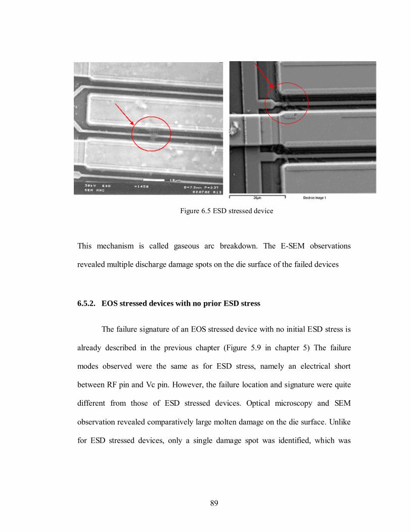
89
This mechanism is called gaseous arc breakdown. The E-SEM observations
revealed multiple discharge damage spots on the die surface of the failed devices
6.5.2. EOS stressed devices with no prior ESD stress
The failure signature of an EOS stressed device with no initial ESD stress is
already described in the previous chapter (Figure 5.9 in chapter 5) The failure
modes observed were the same as for ESD stress, namely an electrical short
between RF pin and Vc pin. However, the failure location and signature were quite
different from those of ESD stressed devices. Optical microscopy and SEM
observation revealed comparatively large molten damage on the die surface. Unlike
for ESD stressed devices, only a single damage spot was identified, which was
Figure 6.5 ESD stressed device

90
easily detectable at low-magnification optical microscopy. The metallization layer
of the EOS stressed device was found to be melted in the vicinity of the Vc pin.
6.5.3. EOS stressed devices with initial ESD stress
Figure 6.6 and Figure 6.7 show an EOS stressed device with initial ESD
stress at 80% of the hard failure threshold voltage. Though failure was caused by
subsequent EOS stress, the failure signature was completely different from those of
EOS-stressed device without initial ESD stress. Failure signature was rather similar
to that of ESD stressed devices, which implies that this device was damaged by
initial low-level ESD stress. This observation supports the existence of latent
damage phenomena in GaAs devices. It may be that from the initial low level ESD
stress, immeasurable and undetectable damage occurs in the device, and from the
subsequent EOS, further localized heating would be focused on the damaged region
Figure 6.6 EOS-stressed device (with initial 80 %of ESD failure threshold voltage)

91
Figure 6.7 EOS-stressed device (with initial 80 %of ESD failure threshold voltage)
Figure 6.8 EOS-stressed device (with initial 20 %of ESD failure threshold voltage)

92
and sufficiently aggravated to cause electrical failure. This is unlikely to occur
during ESD or EOS stress
Figure 6.8 and Figure 6.9 show the EOS stressed devices at 20% and 50% of
the ESD hard failure threshold voltage. The failure signature is completely different
from the previous EOS stressed with initial ESD stress in Figure 6.6 and Figure 6.7.
It is very similar to those of EOS stressed devices with no initial ESD stress in
Figure 5.9 in chapter 5. A single large molten damage was found on each die surface
of damaged device. This indicates that lower multiple stress (20% and 50% of hard
failure threshold voltage) does not affect the device. This is consistent with the
results from subsequent EOS failure threshold test after low-level ESD stress. The
level of initial ESD stress required to induce incipient latent damage is between
50% and 80% of the hard failure threshold voltage.
Figure 6.9 EOS-stressed device (with initial 50 %of ESD failure threshold voltage)

93
6.5.4. Field failed devices
The failure analysis result for field failed devices is presented in the previous
chapter (Figure 5.10 and Figure 5.11 in chapter 5). Field failed devices showed very
similar gate junction failure with that of HBM-stressed devices in the input FET
region, but they also showed a damaged resistor area and mechanical cracks in the
capacitor area, which are not observed in HBM stressed devices. These failure
signatures of field failures have been successfully replicated with EOS-ESD
combined stress test as shown in Figure 6.6 and Figure 6.7. Hence the root cause of
field failure is the EOS stress with prior exposure to ESD stress lower than ESD
failure threshold level.
6.6 Conclusions
Electrostatic discharge (ESD) latent damage effect in a GaAs device was
investigated using electrical overstress (EOS) and ESD stress tests. Failure analysis
and electrical characterization, the failure modes and signatures of EOS stressed
devices with/without prior low-level ESD stress were compared and documented.
In conclusion, no electrical performance degradation was detected even after
as many as 50 low-level ESD discharges at up to 80% of the ESD failure threshold
voltage, indicating that ESD stress lower than ESD failure threshold voltage is not
cumulative under these conditions. The susceptibility of the device to the
subsequent EOS increased after 50 ESD discharges at 80% of the ESD failure
threshold voltage. But no such increase was found after the same number of
94
discharges at 20% or 50% of the ESD failure threshold voltage. This indicates that
there is a specific magnitude of low-level ESD stress above which EOS failure
threshold is reduced without degradation of electrical performance.
Therefore, depending on the magnitude of ESD stress, latent damage can
pose a serious reliability concern in GaAs devices due to potentially higher
susceptibility to EOS and the specific magnitude of low-level ESD stress above
which EOS failure threshold is reduced, which should be considered as one of
important reliability factors in the case of GaAs devices. A proposed screening
method to detect latent damage is an EOS test at reduced voltage level compared to
the EOS failure threshold of the device without prior low-level ESD stress.
In EOS failures occurring at reduced EOS threshold following low-level
ESD stress (80% ESD failure threshold voltage), failure signatures were found to
resemble those of ESD-induced failures. On the other hand, in the case of EOS
failures occurring at normal EOS threshold voltage following 20 % and 50 % of
ESD failure threshold voltage, the failure signatures were very similar to those of
EOS-induced failures without prior ESD stress. Therefore EOS stressed devices
reveal different failure signatures depending on the level of prior ESD stress
voltage.
95
7. ESD FAILURE PREDICTION
In this chapter, the application and development of an electrostatic discharge
(ESD) failure model based on a thermal resistance and capacitance (RC) network is
explained to predict the power-to-failure level. A discussion is given for the
development of the analytical model and a review of previous predictions is given
as well. The correlation of square pulse and real ESD pulse is performed using the
equivalent maximum temperature rise approach. The prediction results are
compared with the experimental results described in the previous chapters (chapter
5 and chapter 6) and used to explain the mechanism of latent damage in GaAs
MESFET devices.
7.1 Background of ESD Failure Prediction and Power-to-Failure
Prediction Models
IC devices are required to remain functional in wide range of ESD stresses,
which subjected to range of current and voltage wave profiles. These electrical wave
profiles combine to produce an instantaneous power profile, P(t), which results in
device heat generation due to Joule heating, and under certain circumstances can
induce a thermal failure. For a given IC device and an electrical stress environment,
their thermal failure threshold is a function of device material properties and device
structures.

96
In previous models and ESD guideline, real ESD stress is considered to be a
equivalent square wave pulse with a duration of 150 ns [59]-[61] in human body
model (HBM) and 100 ns [62] in machine model (MM) for mathematical
convenience, instead of double exponential functions which can express more
realistic ESD pulses. In this chapter, this consideration will be investigated.
ESD or EOS related IC failures can be described by thermal process, as ESD
failures result from localized overheating due to Joule heating [63]. In the localized
region of the IC junction area, the only known way to convert electrical energy to
heat is through Joule heating [64]. When the electrical pulse is applied to IC devices
as a form of ESD or EOS, the temperature in the junction area rises or falls in direct
proportional to the net energy flux crossing the surfaces.
A device can fail at a lower pulse magnitude if the pulse is increased in
duration as the longer pulse period induces more electrical energy resulting in Joule
heating. To quantify this process, ESD failure models have been proposed which
defines linear region of power-to-failure vs. time-to failure as shown in Figure
7.1(b) [65], [66].
Wunsch and Bell [65] first showed that electrical transients could cause
changes in junction parameters due to localized heating. Local temperatures were
shown to become high enough to alter the chemical composition of the junction,
possibly melting and ultimately destroying the crystal structure. Wunsch and Bell
showed that catastrophic damage to semiconductor junctions could be modeled by
using one-dimensional unsteady conductive heat transfer analysis. In their model,
the one-dimensional approximation that takes into consideration the junction area,
97
the thermal constants of the semiconductor material, the temperature rise, and the
energy was provided. Wunsch-Bell model is described by
[ ] 2/1−−= tTTCAP
impf πκρ (eq. 7.1)
where, Pf is the power-to-failure in W, A is the area in cm2, CP is heat capacity in
J/gcm-K and ρ is density in g/cm3. κ is thermal conductivity in W/cm-K, t is the
width of a square pulse, Tm is melting temperature of the junction, Ti is the initial
temperature.
As ESD failure is a thermal process depending on material thermo-physical
properties, in the case of compound semiconductor materials such as gallium
arsenide (GaAs) and silicon germanium (SiGe), which have lower melting
temperatures, lower thermal diffusivity and lower thermal capacitance,
semiconductors heat up faster and melt earlier. Consequently, their susceptibility to
electrical stress is higher as relative to silicon. Based on Wunsch-Bell equation, it is
possible to quantitatively compare and calculate the power-to-failure of various
semiconductor materials, even though this semi-empirical model is experimentally
verified and proved only for silicon devices.
An improved model was proposed by Dwyer [64] to quantify power-to-
failure prediction using 3-dimensional unsteady conductive thermal model. This
model assumes a rectangular-box region of device heating source in the drain-side
junction depletion region of a MOSFET with a spatially uniform, time-invariant
power source (W/cm3) and defines four distinct regions of power-to-failure vs. time-
to failure by solving 3-dimensional heat diffusion equation.

98
Figure 7.1 (a) 3D thermal box region of heat dissipation for power-to-failure prediction in an NMOS transistor, (b) Schematic of power-to-failure vs. width of a square wave pulse
It also assumes constant temperature as a boundary condition on all sides of
the box region and no heating through outside the box. As shown in Figure 7.1, the
length of the box, a, is equal to the width of the device, the width, b, is related to the
gate length, and the depth, c, is approximately equal to the drain diffusion depth.
Such a model is reasonable because simulations and experiments show that the
junction sidewall is the region of highest electric field and current density and is
where most of the potential drop occurs, although the current density is about the
same on the source side, the electric field here is very low.
Although, the previous models show reasonably good agreement with the
experimental data, they have some limitations that affect the accuracy of the model.
In these models, square pulse (constant power) is chosen to provide the same current
amplitude damage level as is found in the ESD stressing models even though the
ESD pulse could be better described by a double exponential function of time and
material properties are assumed to be independent of temperature which is not true.

99
7.2 Heat Flow Model Using Thermal RC Circuit
Due to the structural similarity of electrical and thermal governing equation,
the thermal behavior of a solid media can be modeled by the electrical scheme
shown in Figure 7.2. In electro-thermal analogy, temperature (T), heat flux (Q), Rth
(thermal resistance), and Cth (thermal capacitance) in thermal system are
corresponding to voltage (V), current (I), electrical resistance (R), and electrical
capacitance (C) in electrical system, respectively.
tT
xT
∂∂
⋅=∂∂
α1
2
2
tVRC
xV
∂∂
=∂∂
2
2
(eq. 7.2)
∆y
∆x
∆z
RTxRTx
RTy
RTy
RTz
RTzC
P
x
y z
∆y
∆x
∆z
RTxRTx
RTy
RTy
RTz
RTzC
P
x
y z
x
y z
Figure 7.2 Electrical-thermal equivalent schematic of a solid
The temperature difference resulting from a steady state diffusion of heat
will be related to thermal conductivity (κ), area (A), and the path length (L). The
relationship is like follow.

100
ALqT
κ=∆ (eq. 7.3)
In electro-thermal analogy, thermal resistance Rth and x, y, and z directional thermal
resistance, Rxth, Ryth, Rzth can be defined as
ALRth κ
= , zy
xRxth ∆⋅∆∆
=κ
, xz
yRyth ∆⋅∆∆
=κ
, yx
zRzth ∆⋅∆∆
=κ
(eq. 7.4)
The rate of storage energy in a small volume of solid media, dV is described
by
dVtTCq P ⋅
∂∂
⋅= ρ (eq. 7.5)
Thermal capacitance Cth associated with the heat conduction through the material
volume can be defined in J/K as
dVcC Pth ⋅⋅= ρ (eq. 7.6)
Figure 7.3 Cross-sectional structure and heat source region

101
x
Heat source
Substrate
Schottky contact
GaAs
dx dxdx dx
Ta
GaAs
R
GGaAs CGaAs
CGaAs
g0g0
Ta
GaAs GGaAs
x1 x2L/2-L/2
x
Heat source
Substrate
Schottky contact
GaAs
dx dxdx dx
Ta
GaAs
R
GGaAs CGaAs
CGaAs
g0g0
Ta
GaAs GGaAs
x1 x2L/2-L/2
Figure 7.4 Electrical-thermal analogy modeling for heat source region
Based on electrical-thermal analogy, RC thermal network approach for
ESD/EOS has been previously developed [68]-[70]. In this study, similar modeling
methodology is used. Figure 7.3 shows the cross-sectional view and dimension of
heat source for the area of interest of IC device. Heat source region is defined in
Figure 7.3 and Figure 7.4. Its x-directional length, ∆x=x2-x1 is assumed to be equal
to the length of high field region [71] and depth of heat source region is assumed to
be equal to the depletion region of the device [64] . The z-directional depth of heat
source is the channel width. In this model, heat flow through the interconnects and
substrate area is negligible and insulating boundary conditions are assumed at the
boundaries of end of junction edges, x = ±L/2. Power input is lumped into the whole
heat source region and RC thermal network analogy modeling for heat source region
is shown in Figure 7.4.

102
In Figure 7.4, R is the thermal resistance per unit length, C and G are the
thermal capacitance per unit length and thermal conductance per unit length
respectively. The nodal equation of heat source region in Figure 7.4 can be given by
[70]
),(),(),( sxRdxQsdxxTsxT =+∆−∆ and (eq. 7.7(a))
dxsgsdxxTdxsYsdxxQsxQ )(),()(),(),( 0−+∆=+− (eq. 7.7(b))
where, ∆T(x,s) is the temperature rise and Q(x,s) is the heat flow at point x. The heat
source is represented by g0(s)dx and Y(s) is total equivalent admittance per unit
length. For the simpler calculation, all expressions are given in Laplace domain.
The power source g0 in the heat source region is given by
],[)(2],[
21012
210 xxSq
xxxxSP
g ⋅=−
⋅= (eq. 7.8)
where, P is input power, S[x1, x2] is unit step function in the heat source region from
x1 to x2.
By taking the limit dx -> 0 in equations above, two equations can be
combined into the following simple second-order differential equation.
s
sRgsxTsRY
xsxT )(
),()(),( 0
2
2
−∆=∂
∆∂ (eq. 7.9)
Using the series expansion method, this equation can be solved and transformed into
time domain by inverse Laplace transform like follows;
∑ ∑∞
=
∞
=
Γ+Γ=∆,..5,3,1 ...4,2,0
)()cos()()sin(),(n n
nn tL
xntL
xntxT ππ (eq. 7.10)

103
where, ∞=+
=Γ ........2,1,0,)]([
)( 2 nsRYs
RDs
n
nn γ
L
nn
πγ = ,
⎥⎦⎤
⎢⎣⎡ −= )sin()sin(2 120
Lxn
Lxn
nqDn
πππ
for n=1,3,5….
⎥⎦
⎤⎢⎣
⎡ −= )cos()cos(2 210
Lxn
Lxn
nq
Dnππ
π for n=0, 2,4,6…
Γ(s) is the Laplace transform of the equation Γ(t).
7.3 Power-to-failure generation
Using the RC network model described in section 7.2, the relationship
between power-to-failure and pulse duration can be generated for various types of
devices. Figure 7.5 shows the simulated time dependence of maximum temperature.
In this plot, tf (pulse duration of square pulse) is defined as the point at which the
maximum junction temperature equals to the device melting temperature which
infers the catastrophic failure of the device. The plot shows that different power
levels result in different temperature rise profile and pulse duration that causes
device melting temperature.

104
0
500
1000
1500
2000
2500
3000
1.E-12 1.E-11 1.E-10 1.E-09 1.E-08 1.E-07 1.E-06 1.E-05
Time (sec)
Tem
pera
ture
rise
(C)
0.1W0.02W0.05
Melting temperature
Tf
Figure 7.5 Power-to-failure and Time-to-Failure (Tf) Determination
1.0E-03
1.0E-02
1.0E-01
1.0E+00
1.0E+01
1.0E-09 1.0E-08 1.0E-07 1.0E-06 1.0E-05
Time (sec)
Failu
re p
ower
(W)
Analytical model
Experiments
Figure 7.6 Power-to-failure versus pulse duration, measurement versus prediction for a silicon device
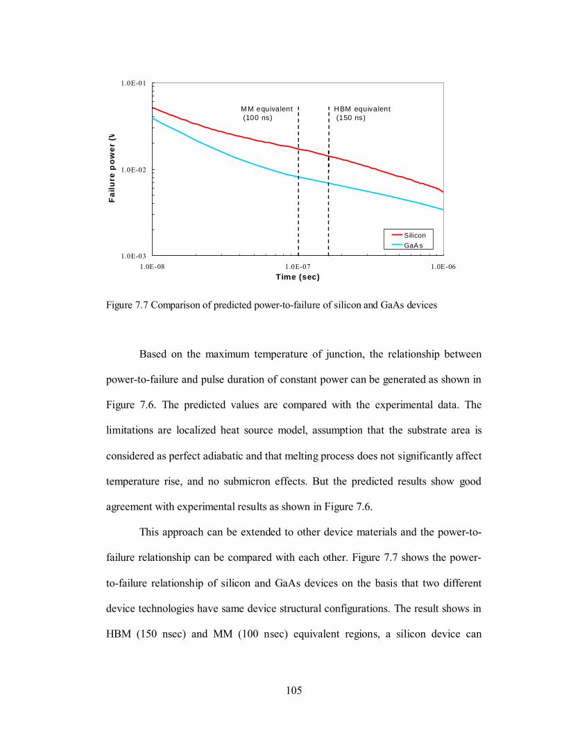
105
1.0E-03
1.0E-02
1.0E-01
1.0E-08 1.0E-07 1.0E-06Time (sec)
Failu
re p
ower
(W
SiliconGaA s
MM equivalent (100 ns)
HBM equivalent (150 ns)
Figure 7.7 Comparison of predicted power-to-failure of silicon and GaAs devices
Based on the maximum temperature of junction, the relationship between
power-to-failure and pulse duration of constant power can be generated as shown in
Figure 7.6. The predicted values are compared with the experimental data. The
limitations are localized heat source model, assumption that the substrate area is
considered as perfect adiabatic and that melting process does not significantly affect
temperature rise, and no submicron effects. But the predicted results show good
agreement with experimental results as shown in Figure 7.6.
This approach can be extended to other device materials and the power-to-
failure relationship can be compared with each other. Figure 7.7 shows the power-
to-failure relationship of silicon and GaAs devices on the basis that two different
device technologies have same device structural configurations. The result shows in
HBM (150 nsec) and MM (100 nsec) equivalent regions, a silicon device can

106
withstand higher power density than a GaAs device (approximately 1.9 times higher
in HBM and 2.3 times higher in MM).
7.4 Failure prediction for ESD pulse
Based on the power-to-failure approach (temperature rise prediction due to
the constant power), failure prediction can be extended to ESD pulses. By lumped
element model and principal waveform of ESD pulse in ESD test standards, the
HBM ESD pulse can be described by
[ ] )exp()exp(1)(RCt
LRt
RVtI −−−= (eq. 7.11)
where, V is voltage of HBM ESD pulse, R, C, and L are resistance, capacitance, and
inductance of HBM respectively.
Figure 7.8 HBM current waveform for failure prediction
Simulated profiles
Measured at 2000 V

107
The rise time of the waveform is given by 2L/R. Figure 7.8 shows the current
waveform of HBM pulses for different HBM voltage levels. Solid lines are from
circuit simulations and compared with measured data for 2,000 V which is dotted
line. Simulated current profiles show good agreement with the measurement profile.
The analysis results (Figure 7.9) show that maximum junction temperature
rise depends on the input ESD voltage stress level. The prediction of maximum
temperature rise is given for each HBM ESD pulses. As shown in this plot, at the
HBM ESD failure threshold voltage condition (3,500 V) which was determined in
previous chapter 5.3 and 6.4 by experiments, the temperature of junction area
exceeds the melting temperature, which means the catastrophic failure of the
devices occurs.
Figure 7.9 Temperature rise profile from the HBM ESD pulses

108
In case of 80 % of failure threshold voltage (2,800 V), as shown in the plot,
the temperature does not reach the device melting temperature which means
catastrophic failure does not occur, but it exceeds the intrinsic temperature of the
device.
The intrinsic temperature is the temperature at which the intrinsic carrier
concentration exceeds the background doping concentration and at this point,
thermal runaway is triggered [72], [73]. As the temperature increases from the room
temperature, the resistivity also increases due to mobility degradation. However, the
intrinsic carrier concentration increases with temperature, and when it finally meets
and exceeds the background doping concentration level, the resistivity of the
junction reaches a maximum and then starts decreasing, and leading to an even
higher current level and thus more heating. In this condition, if there is sufficient
power dissipation from the ESD pulse, the local temperature will exceed the device
melting temperature.
Although the resistivity in the hot spot area decreases, the surrounding high
temperature region still has a high resistivity and the overall device resistance may
not decrease until there is a large area in which the intrinsic concentration is larger
than the doping. Thermal runaway results in the creation of the hot spot during a
very short pulse period, but it is not sufficient to cause catastrophic damage. In the
hot spot, the heat affected zone can create latent damage in the device junction area
and increase the susceptibility to the subsequent EOS stress as described in chapter
6.
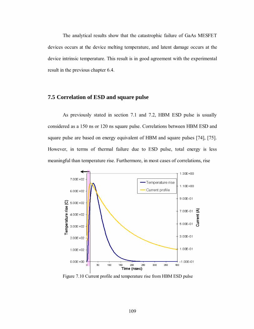
109
The analytical results show that the catastrophic failure of GaAs MESFET
devices occurs at the device melting temperature, and latent damage occurs at the
device intrinsic temperature. This result is in good agreement with the experimental
result in the previous chapter 6.4.
7.5 Correlation of ESD and square pulse
As previously stated in section 7.1 and 7.2, HBM ESD pulse is usually
considered as a 150 ns or 120 ns square pulse. Correlations between HBM ESD and
square pulse are based on energy equivalent of HBM and square pulses [74], [75].
However, in terms of thermal failure due to ESD pulse, total energy is less
meaningful than temperature rise. Furthermore, in most cases of correlations, rise
Figure 7.10 Current profile and temperature rise from HBM ESD pulse

110
(a) Temperature rise from square pulse (b) Temperature rise from HBM ESD
time
Tem
pera
ture
rise
TMAX
tequiv time
Tem
pera
ture
rise
tMAX_HBM
(a) Temperature rise from square pulse (b) Temperature rise from HBM ESD
time
Tem
pera
ture
rise
TMAX
tequiv time
Tem
pera
ture
rise
tMAX_HBMtime
Tem
pera
ture
rise
TMAX
tequiv time
Tem
pera
ture
rise
tMAX_HBM
Figure 7.11 Temperature rise from HBM ESD and square pulse
time of HBM pulse is ignored, because rise time (around 10~15 ns) is much lower
than decay time (around 300~400 ns). In terms of energy equivalent, this
assumption may be acceptable, but in the temperature rise from the ESD pulse,
analysis result (Figure 7.10) indicates that approximately 50 % of temperature rise
occurs during the rise time. This is illustrated by the arrow which indicates the
region of rise time area. This means the rise time region of the ESD pulse should be
considered in the correlation.
In the correlation proposed in this study, the maximum temperature rise has
been chosen as a correlation factor. The concept of the correlation is shown in
Figure 7.11. From the prediction of maximum temperature rise for ESD and square
pulses, the equivalent square pulse duration that causes same temperature rise from
real ESD pulses is determined.

111
In order to correlate HBM ESD and square pulses, several assumptions need
to be made. (1) Both HBM ESD and square pulses produce identical failure
mechanisms when the maximum temperature reaches the device melting
temperature. Although still controversial, Bridgewood [60], [76] previously showed
this assumption is true based on experiments. (2) In case of square pulse, it is
assumed that the maximum temperature occurs at the end of pulse. (3) The current
from square pulse is assumed HBM peak voltage (VHBM) divided by HBM
resistance (1,500Ω), which is generally accepted and experimentally proved by
Amerasekera [59].
Figure 7.12 Correlation result for HBM ESD pulse and square pulse
Based on the three assumptions and equivalent maximum temperature rise
approach, if we let equivalent pulse length of square wave pulse, tequiv, maximum
temperature rise from the HBM pulse TMAX, and the time at which the maximum

112
temperature reaches tMAX_HBM, at time tequiv, the temperature rise from the square
pulse needs to be same with maximum temperature rise from HBM pulses (Figure
7.11).
The correlation result is shown in Figure 7.12. The correlation of square
pulse and HBM ESD pulse has been performed using the equivalent maximum
junction temperature rise approach. The result suggests that HBM stress needs to be
considered to be square pulse with 80 ns duration rather than 120 or 150 ns as
suggested in other published studies.
7.6 Conclusions
The predicted temperature rise using RC thermal network was in good
agreement with experimental measurements for HBM ESD stress conditions.
Comparison of predicted power-to-failure for GaAs and silicon devices showed that
in the HBM and MM equivalent regions (150 nsec-HBM, 100 nsec-MM), a silicon
device can withstand approximately double the power density than a GaAs device.
The predicted temperature rise indicates that at the ESD failure threshold
voltage level for GaAs MESFET devices, the maximum junction temperature of the
device exceeds the device melting temperature. At the 80 % of failure threshold
voltage level, the maximum temperature does not reach the melting temperature but
exceeds device intrinsic temperature, which implies the latent damage of a GaAs
MESFET device occurs when the temperature of the device junction exceeds the
device intrinsic temperature.

113
Equivalent maximum temperature rise approach was applied to correlate the
square pulse and HBM ESD pulses. The correlation results suggest that HBM stress
needs to be considered for a square pulse with 80 ns duration which is smaller than
150 or 120 ns value suggested in literature. Furthermore, the equivalent square wave
pulse duration should not be considered as a fixed value as ESD stress varies.
114
8. CONTRIBUTIONS
GaAs and SiGe are becoming more popular in advanced technologies but
their susceptibility to electrostatic discharge (ESD) and electrical overstress (EOS)
is not well understood. This dissertation identifies the effects of ESD and EOS
phenomena on GaAs and SiGe semiconductor devices. The damage characterization
due to both ESD and EOS is performed and an approach to the assess root cause of
the failure is discussed. The effect of ESD latent damage is presented. Thermal RC
network analysis is shown to predict the ESD failure threshold level on various
types of IC devices.
The contributions of this thesis are:
1. Characteristics of internal damage caused by ESD test models and EOS stress in
GaAs and SiGe devices have been identified and the failure signatures have been
correlated with field failures. I found that even though different ESD test models,
EOS, and field failure reveal the same failure mode, the failure signatures are
different. This can provide a means to identify root causes.
2. I experimentally showed that ESD stresses lower than the ESD failure threshold
voltage does not cause any change in the ESD failure threshold or electrical
performance degradation.
3. I discovered that prior ESD stress, lower than the ESD failure threshold voltage,
can increase the susceptibility of a GaAs MESFET devices to subsequent EOS

115
stress without observable degradation of electrical performance. Such an effect
varies depending on the level of prior ESD stress.
4. EOS failures were found to be dependent on the level of the prior ESD stress
voltage. In EOS failures occurring at reduced EOS threshold following low-level
ESD stress, failure signatures were found to resemble those of ESD-induced
failures. On the other hand, in case of EOS failures occurring at normal EOS
threshold voltage, the failure signatures are very similar to those of EOS-induced
failures without prior ESD stress.
5. I demonstrated correlation of ESD induced EOS failure of GaAs MESFET
devices with actual field failures for the first time. This type of field failure has
been successfully replicated by EOS stress test with prior ESD stress testing.
6. ESD pulses which generate temperature above the device intrinsic temperature
can cause latent damage in GaAs MESFET devices.
116
9. REFERENCES
[1] Green, T. J. and Denson, W.K. “Review of EOS/ESD field failures in military
equipment,” Proceedings of 10th EOS/ESD Symposium, pp. 7-14, 1988.
[2] Diaz, C., et al, “Electrical overstress (EOS power profiles: A guideline to
qualify EOS hardness of semiconductor devices”, Proceedings of 14th
EOS/ESD Symposium, pp. 88-94, 1992.
[3] Electrostatic Discharge Association homepage, http://www.esda.org, 2003.
[4] Vinson, J. E. and Liou, J. J., “Electrostatic Discharge in Semiconductor
Devices: An Overview”, Proceedings of The IEEE, vol. 86, No. 2, Feb. 1998.
[5] Greason, W. D., and Castle, G, S. P., ‘The Effect of ESD on Microelectronics
Devices – A Review’, IEEE Transactions on Industrial Applications, vol. IA-
20, p. 247-252, 1984.
[6] Electrostatic Discharge Control Handbook for Protection of Electrical and
Electronic Parts, Assemblies and Equipment (Excluding Electrically Initiated
Explosive Devices) (Metric), July 31, 1994.
[7] Chemelli, R. G. et al, “ESD by Static Induction”, Proceedings of EOS/ESD
Symposium, pp. 29-36, 1983.
[8] Amerasekera, E. A, ESD in Silicon Integrated Circuits, John Wiley & Sons,
New York, 1995.
[9] Amerasekera, E. A. and Najm, F. N., Failure Mechanisms in Semiconductor
Devices, John Wiley & Sons, New York, 1997
[10] Roesch, W. J. et al, “GaAs IC Reliability, The Next Generation”, 15th Annual
GaAs IC Symposium, pp. 103-106, 1993.
[11] Pecht M. and Ramappan, V., “Review of Electronic System and Device Field
Failure Returns”, IEEE Transactions on CHMT, Vol. 15, No. 6, pp. 1160-1164,
1992.
[12] Halperin, S., Guidelines for Static Control Management, Eurostat, 1990.

117
[13] Pecht, M. G., R. Radojcic, and G. Rao, Guidebook for Managing Silicon Chip
Reliability, CRC Press, Boca Raton, Florida, 1999.
[14] Vinson, J. E. and Liou, J. J., “Electrostatic Discharge in Semiconductor
Devices: Protection Techniques,” Proceedings of the IEEE, vol. 88, pp. 1878-
1900, 2000.
[15] Russell, W, “Protecting Portable Devices from ESD Damage”, Communication
Systems Design Magazine, April, 1997.
[16] Overview of Quality and Reliability Issues in the National Technology
Roadmap for Semiconductors, SEMATECH Technology Transfer #
98013448A-TR, pp. 4, Date of Release: Jan-30, 1998.
[17] Kreiger, G., “ESD in Integrated Circuits--General Introduction,” ESD in
Integrated Circuits Short Course Proceedings, sponsored by University of
California, 1992.
[18] JEDEC Solid State Technology Association, JEDEC STANDARD No.22-
A114-B, “Electrostatic Discharge Sensitivity Testing Human Body Model”,
Arlington, VA, June 2000.
[19] Electronic Industries Association, EIA/JEDEC No.22-A115, “Electrostatic
Discharge Sensitivity Testing Machine Model”, Arlington, VA, October 1997.
[20] JEDEC Solid State Technology Association, JEDEC Standard No. 22-C101-A,
“Field-Induced Charged-Device Model Test Method for Electrostatic-
Discharge-Withstand Thresholds of Microelectronic Components, Arlington,
VA, June 2000.
[21] Middendorf, M. and Hanksen, T., “Observed physical defects and failure
analysis of EOS/ESD on MOS devices”, International Symposium for Test &
Failure Analysis, pp. 205-213, 1984.
[22] Melchior, H. and Strutt, M.J.O., “Secondary Breakdown in Transistors”,
Proceedings of IEEE, pp. 439-440, 1964.
[23] Mayaram, K. et al, “Electothermal Simulation Tools for Analysis and Design
of ESD Protection Devices”, IEDM Tech. Dig., pp. 909-912, 1991.

118
[24] Polgreen T.L. and Chatterjee, A., “ Improving the ESD Failure Threshold of
Silicided n-MOS Output Transistors by Ensuring Uniform Current Flow”,
IEEE Transaction on Electronic Devices, vol. ED-39, pp. 379-388, 1992.
[25] Thomas W Lee, “ESD and EOS – There Is a Difference”, Commercialization
of Military and Space Electronics Conference, pp. 49-65, February, 2002
[26] Kelly, M. et al, “Comparison of Electrostatic Discharge Models and Failure
Signatures for CMOS Integrated Circuit Devices”, Proceedings of EOS/ESD
Symposium, pp. 176-185, 1995.
[27] Speakman, T. S., “A Model for Failure of Bipolar Silicon Integrated Circuits
Subjected to Electrostatic Discharge”, Proceedings of International Reliability
Physics Symposium, pp. 60-69, 1974.
[28] Ker, M. D., et al, “ESD Test Methods on Integrated Circuits: An Overview”,
IEEE International Conference on Electronics, Circuits and Systems, vol. 2, pp.
1011-1014, 2001.
[29] Bossard, P. R. et al, 'ESD Damage from Triboelectrically Charged IC Pins',
Proceedings of EOS/ESD Symposium, pp. 17-22, 1980.
[30] Stephen G. Beebe, ‘Characterization, Modeling, and Design of ESD Protection
Circuits’, Ph. D. Thesis, Stanford University, 1998
[31] Chaine, M. et al, 'Investigation into Socketed CDM Tester Parasitics',
Proceedings of EOS/ESD Symposium., pp. 301-310, 1998
[32] Hutchins, D. W., 'On-chip Protection, A Self-Defense', ProTek Devices
Technical Notes, pp. 8.1-803, 1996.
[33] Electrostatic Discharge Association Homepage (http://www.ESDA.org), 2004.
[34] Areve, D.W., Field Effect Devices and Applications, pp. 315, 1998.
[35] Voldman, S. et al “ESD robustness of BiCMOS SiGe technology,” in
Proceedings of IEEE Bipolar/BiCMOS Circuits and Technology Meeting, pp.
214–217.2000.
[36] “SiGe Technology-The Enabling Technology for Entering HF Markets”,
Technical Report of Flash Communication Inc. 2002.
119
[37] Tatsumi, et al, “Si/Ge0.3Si0.7/Si heterojunction bipolar transistor made with Si
molecular beam epitaxy,” Applied Physics Letters, 52, 2239, 1988.
[38] Patton, G. L., et al, “Silicon-germanium base heterojunction transistor by
molecular beam epitaxy,” IEEE Electron Device Letters, 9, 165, 1988.
[39] Temkin, H., et al, “GexSi1-x strained layer heterostructure bipolar transistors,”
Applied Physics Letters, 52, 1089, 1988.
[40] Dunn, J., Harame, D., et al, “Trends in Silicon Germanium BiCMOS
Integration and Reliability,” Proceedings of the annual international reliability
physics symposium, San Jose, CA, pp. 237–242, IEEE 2000.
[41] Voldman, et al, “Electrostatic Discharge and High current Pulse
Characterization of Epitaxial-base SiGe Heterojunction Bipolar Transistors,”
Proceedings of the 38th IEEE Annual International Reliability Physics
Symposium, San Jose, CA, 2000.
[42] Electronic News, “TI innovates with SiGe process,”
[43] Christou, A., Reliability of Gallium Arsenide MMICs (Design and
Measurement in Electronic Engineering), John Wiley & Sons, 1991.
[44] Chase, E. W., “Theoretical Study of Expected EOS/ESD Sensitivity of Ш-V
Compound Semiconductor Devices”, Proceedings of EOS/ESD Symposium,
pp. 65-69, 1988.
[45] Ragle, D. et al, “ESD Effects on GaAs MESFET Lifetime”, 31st Annual
Proceedings of International Reliability Physics Symposium, pp. 352-362,
1993.
[46] Yamada, F.M. et al, “ESD Sensitivity Study of Various Diode Protection
Circuits Implemented in a Production 1 µm GaAs HBT technology”,
Proceedings of GaAs Reliability Workshop, pp. 139-146, 1999.
[47] Rubalcava, A. L. et al, “Electrostatic Discharge Effects on GaAs Integrated
Circuits”, Proceedings of EOS/ESD Symposium, pp. 159-171, 1986.
[48] Voldman, S., “ESD: Where Are We Heading? – Part2”, Technical Paper of
ESD Journal, 2002.

120
[49] McAteer, O. J. t al “Identification of Latent ESD Failures”, Proceedings of
EOS/ESD Symposium, pp. 54-57, 1980.
[50] Song, M. et al, “Quantifying ESD/EOS Latent Damage and Integrated Circuit
Leakage Currents”, Proceedings of EOS/ESD Symposium, pp. 304-310, 1995.
[51] Anthony L. Rubalcava and William J. Roesch, “Lack of Latent and
Cumulative ESD Effects on MESFET-Based GaAs ICs”, Proceedings of
EOS/ESD Symposium, pp. 62-64, 1988.
[52] Wu, J. et al, “Breakdown and Latent Damage of Ultra-Thin Gate Oxides under
ESD Stress Conditions”, Proceedings of EOS/ESD Symposium, pp. 287-295,
1995.
[53] Reiner, J. C., “Latent Gate Oxide Defects Caused by CDM-ESD”, Proceedings
of EOS/ESD Symposium, pp 311-321, 1995.
[54] Salome, P. et al, “An Attempt to Explain Thermally Induced Soft Failures
during Low Level ESD Stresses: Study of the Differences between Soft and
Hard NMOS Failures”, Proceedings of EOS/ESD Symposium, pp 337-345,
1997.
[55] Anthony L. Rubalcava and William J. Roesch, “Lack of Latent and
Cumulative ESD Effects on MESFET-Based GaAs ICs”, Proceedings of
EOS/ESD Symposium, pp. 62-64, 1988.
[56] Ragle, D. et al, “ESD Effects on GaAs MESFET Lifetime”, 31st Annual
Proceedings of International Reliability Physics Symposium, pp. 352-362,
1993.
[57] Crockett R. et al, “ESD Sensitivity and Latency Effects in Some HCMOS ICs”,
Proceedings of EOS/ESD Symposium, pp.196-201, 1994.
[58] Greason, W. D., Kucerovsky, J. and Chum, K., “Latent Failures Due to ESD in
CMOS Integrated Circuits”, IEEE Conference on Industry Applications
Society, pp. 1927-1933, Oct. 1989.
[59] Amerasekera, A. et al, “The impact of Technology scaling on ESD Robustness
and Protection Circuit Design”, Proceedings of EOS/ESD Symposium, pp.
237-245, 1994.

121
[60] Bridgewood, A. et al, “A Comparison of Threshold Damage Processes in
Thick Field Oxide Protection Devices Following Square Pulse and HBM
Injection”, Proceedings of EOS/ESD Symposium, pp. 129-136, 1988.
[61] Barth, J. E. et al, “TLP Calibration, Correlation, Standards, and New
Techniques”, IEEE Transactions on Electronics Packaging Manufacturing, vol.
24, No. 2, pp. 99-108, 2001.
[62] Banerjee K. et al, “High-current failure model for VLSI interconnects under
short-pulse stress conditions”, IEEE Electron Device Letters, vol. 18, pp. 405-
407, 1997.
[63] Smith, J. S., “General EOS/ESD Equation”, Proceedings of EOS/ESD
Symposium, pp. 59-67, 1997.
[64] Dwyer, V. et al, “Thermal Failure in Semiconductor Devices”, Solid State
Electron, Vol. 33. No. 5, pp. 553-560, 1990.
[65] Wunsch, D. C. et al, “Determination of Threshold Voltage Levels of
Semiconductor Diodes and Transistors Due to Pulsed Voltages”, IEEE
Transactions on Nuclear Science, vol. NS-15, No. 6, pp. 244-259, 1968.
[66] Tasca, D.M, “Pulse Power Failure Modes in Semiconductors”, IEEE
Transactions on Nuclear Science, vol.ns-17, no.6, pp. 364-372, 1970.
[67] Siemsen, K, “EOS Test Limits for Manufacturing Equipment”, Proceedings of
EOS/ESD Symposium, pp. 168-173, 1987.
[68] Bielefeld, J. et al, “Dynamic SPICE-Simulation of the Electrothermal Behavior
of SOI MOSFET’s”, IEEE Transactions on Electron Devices, vol. 42, no. 11,
pp. 1968-1974, 1995.
[69] Chiang, T. et al, “Compact Modeling and SPICE-based Simulation for
Electrothermal Analysis of Multilevel ULSI Interconnects”, IEEE/ACM
International Conference on Computer Aided Design, pp. 165-172, 2001.
[70] Raha, P., et al, “ESD Robustness Prediction and Protection Device Design in
Partially Depleted SOI Technology”, Microelectronics Reliability, vol.38,
no.11, pp. 1723-1731, 1998.

122
[71] Ko, P. K., “Approaches to Scaling”, Advanced MOS Device Physics, vol. 18,
N. G. Einspruch, Ed. New York, 1989.
[72] Amerasekera, A. and Seitchik, J., ‘Electothermal Behavior of Deep Submicron
nMOS Transistors Under High Current Snapback Conditions’, International
Electron Devices Meeting Technical Digest, pp. 455-458, 1994.
[73] Amerasekera, A. et al, ‘Characterization and Modeling of Second Breakdown
in NMOS for the Extraction of ESD-Related Process and Design Parameters’,
IEEE Electron Devices, vol. 38, no. 9, pp. 2161-2168, 1991.
[74] Barth, J. and Richner, J, “Correlation Considerations: Real HBM to TLP and
HBM Testers”, Microelectronics Reliability vol. 42, pp. 909-917, 2002.
[75] Dwyer, V. M., “Electrostatic Discharge Thermal Failure in Semiconductor
Devices”, IEEE Transactions on Electron Devices, vol. 37, no. 11, 1990.
[76] Amerasekera, A. et al, “An Analysis of Low Voltage ESD Damage in
Advanced CMOS Processes”, Proceedings of EOS/ESD Symposium, pp. 143-
150, 1990.