Current noise in topological Josephson junctions
Julia S. Meyer with Driss Badiane, Leonid Glazman, and Manuel Houzet
INT Seattle Workshop on Quantum Noise
May 29, 2013

Motivation
• active search for Majorana fermions in superconducting hybrid structures
proposed signatures:
• zero-energy bound state (visible in tunneling DoS) • fractional AC Josephson effect?
→ study properties of a biased topological Josephson junction
INT Seattle - May 29, 2013 2

Topological Phases
INT Seattle - May 29, 2013 3
BEST KNOWN EXAMPLE: QH system NOVEL ASPECTS: • time-reversal symmetry • strong spin-orbit interaction → band inversion
Example: HgTe/CdTe quantum wells Koenig et al., Science 421, 766 (2007)
[also InAs/GaSb Knez, Du & Sullivan, PRL 107, 136603 (2011)]
5
fluenced by a TR symmetry-breaking magnetic field. Furthertransport measurements (Roth et al., 2009) reported uniquenonlocal conduction properties due to the helical edge states.The QSH insulator state is invariant under TR, has a charge
excitation gap in the 2D bulk, but has topologically pro-tected 1D gapless edge states that lie inside the bulk insu-lating gap. The edge states have a distinct helical prop-erty: two states with opposite spin polarization counter-propagate at a given edge (Kane and Mele, 2005; Wu et al.,2006; Xu and Moore, 2006). For this reason, they are alsocalled helical edge states, i.e. the spin is correlated with thedirection of motion(Wu et al., 2006). The edge states comein Kramers doublets, and TR symmetry ensures the crossingof their energy levels at special points in the Brillouin zone.Because of this level crossing, the spectrum of a QSH insu-lator cannot be adiabatically deformed into that of a topo-logically trivial insulator without helical edge states. There-fore, in this precise sense, the QSH insulator represents a newtopologically distinct state of matter. In the special case thatSOC preserves a U(1)s subgroup of the full SU(2) spin rota-tion group, the topological properties of the QSH state can becharacterized by the spin Chern number (Sheng et al., 2006).More generally, the topological properties of the QSH stateare mathematically characterized by a Z2 topological invari-ant (Kane and Mele, 2005). States with an even number ofKramers pairs of edge states at a given edge are topologi-cally trivial, while those with an odd number are topologicallynontrivial. The Z2 topological quantum number can also bedefined for generally interacting systems and experimentallymeasured in terms of the fractional charge and quantized cur-rent on the edge (Qi et al., 2008), and spin-charge separationin the bulk (Qi and Zhang, 2008; Ran et al., 2008).In this section, we shall focus on the basic theory of the
QSH state in the HgTe/CdTe system because of its simplicityand experimental relevance, and provide an explicit and ped-agogical discussion of the helical edge states and their trans-port properties. There are several other theoretical propos-als for the QSH state, including bilayer bismuth (Murakami,2006), and the “broken-gap” type-II AlSb/InAs/GaSb quan-tum wells (Liu et al., 2008). Initial experiments in theAlSb/InAs/GaSb system already show encouraging signa-tures (Knez et al., 2010). The QSH system has also been pro-posed for the transition metal oxide Na2IrO3 (Shitade et al.,2009). The concept of fractional QSH state was proposedat the same time as the QSH (Bernevig and Zhang, 2006),and has been investigated theoretically in more details re-cently (Levin and Stern, 2009; Young et al., 2008).
A. Effective model of the two-dimensional time-reversalinvariant topological insulator in HgTe/CdTe quantumwells
In this section we review the basic electronic structure ofbulk HgTe and CdTe, and present a simple model first in-troduced by Bernevig, Hughes and Zhang (Bernevig et al.,
FIG. 2 (a) Bulk band structure of HgTe and CdTe; (b) schematic pic-ture of quantum well geometry and lowest subbands for two differentthicknesses. From Bernevig et al., 2006.
2006) (BHZ) to describe the physics of those subbands ofHgTe/CdTe quantum wells that are relevant for the QSH ef-fect. HgTe and CdTe crystallize in the zincblende lattice struc-ture. This structure has the same geometry as the diamondlattice, i.e. two interpenetrating face-centered-cubic latticesshifted along the body diagonal, but with a different atomon each sublattice. The presence of two different atoms perlattice site breaks inversion symmetry, and thus reduces thepoint group symmetry from Oh (cubic) to Td (tetrahedral).However, even though inversion symmetry is explicitly bro-ken, this only has a small effect on the physics of the QSHeffect. To simplify the discussion, we shall first ignore thisbulk inversion asymmetry (BIA).For both HgTe and CdTe, the important bands near
the Fermi level are close to the ! point in the Brillouinzone [Fig. 2(a)]. They are a s-type band (!6), and a p-typeband split by SOC into a J = 3/2 band (!8) and a J = 1/2band (!7). CdTe has a band ordering similar to GaAs with a s-type (!6) conduction band, and p-type valence bands (!8,!7)which are separated from the conduction band by a large en-ergy gap (! 1.6 eV). Because of the large SOC present inthe heavy element Hg, the usual band ordering is inverted:the negative energy gap of "300 meV indicates that the !8
band, which usually forms the valence band, is above the !6
band. The light-hole !8 band becomes the conduction band,the heavy-hole band becomes the first valence band, and thes-type band (!6) is pushed below the Fermi level to lie be-tween the heavy-hole band and the spin-orbit split-off band(!7) [Fig. 2(a)]. Due to the degeneracy between heavy-holeand light-hole bands at the ! point, HgTe is a zero-gap semi-conductor.When HgTe-based quantum well structures are grown, the
peculiar properties of the well material can be utilized to tunethe electronic structure. For wide QW layers, quantum con-finement is weak and the band structure remains “inverted”.
8
The coefficients a, b, c, d can be determined by imposing theopen boundary condition !(0) = 0. Together with the nor-malizability of the wave function in the region x > 0, theopen boundary condition leads to an existence condition forthe edge states: !"1,2 < 0 (c = d = 0) or !"1,2 > 0(a = b = 0), where ! stands for the real part. As seen fromEq. (15), these conditions can only be satisfied in the invertedregime when M/B > 0. Furthermore, one can show thatwhen A/B < 0, we have !"1,2 < 0, while when A/B > 0,we have!"1,2 > 0. Therefore, the wave function for the edgestates at the ! point is given by
!0(x) =
!
a"
e!1x " e!2x#
#+, A/B < 0;
c"
e!!1x " e!!2x#
#!, A/B > 0.(16)
The sign of A/B determines the spin polarization of the edgestates, which is key to determine the helicity of the DiracHamiltonian for the topological edge states. Another im-portant quantity characterizing the edge states is their decaylength, which is defined as lc = max
$
|!"1,2|!1%
.The effective edge model can be obtained by projecting the
bulk Hamiltonian onto the edge states "" and "# defined inEq. (11). This procedure leads to a 2 # 2 effective Hamil-tonian defined by H"#
edge(ky) = $""|&
H0 + H1
'
|"#%. Toleading order in ky , we arrive at the effective Hamiltonian forthe helical edge states:
Hedge = Aky$z . (17)
For HgTe QWs, we have A & 3.6 eV·A (Konig et al., 2008),and the Dirac velocity of the edge states is given by v =A/! & 5.5# 105 m/s.The analytical calculation above can be confirmed by exact
numerical diagonalization of the Hamiltonian (2) on a stripof finite width, which can also include the contribution ofthe %(k) term [Fig. 4]. The finite decay length of the heli-cal edge states into the bulk determines the amplitude for in-teredge tunneling (Hou et al., 2009; Strom and Johannesson,2009; Tanaka et al., 2009; Teo and Kane, 2009; Zhou et al.,2008; Zyuzin and Fiete, 2010).
C. Physical properties of the helical edge states
1. Topological protection of the helical edge states
From the explicit analytical solution of the BHZ model,there is a pair of helical edge states exponentially localizedat the edge, and described by the effective helical edge the-ory (17). In this context, the concept of “helical” edgestate (Wu et al., 2006) refers to the fact that states with op-posite spin counter-propagate at a given edge, as we see fromthe edge state dispersion relation shown in Fig. 4(b), or thereal space picture shown in Fig. 1(b). This is in sharp contrastto the “chiral” edge states in the QH state, where the edgestates propagate in one direction only, as shown in Fig. 1(a).
−0.02 −0.01 0 0.01 0.02−0.05
0
0.05
k (A−1)
E(k)
(eV)
−0.02 −0.01 0 0.01 0.02−0.05
0
0.05
k (A−1)
E(k)
(eV)
(a)
(b)
FIG. 4 Energy spectrum of the effective Hamiltonian (2) in a cylin-der geometry. In a thin QW, (a) there is a gap between conductionband and valence band. In a thick QW, (b) there are gapless edgestates on the left and right edge (red and blue lines, respectively).The dashed line stands for a typical value of the chemical potentialwithin the bulk gap. Adapted from Qi and Zhang, 2010.
In the QH effect, the chiral edge states can not be backscat-tered for sample widths larger than the decay length of theedge states. In the QSH effect, one may naturally ask whetherbackscattering of the helical edge states is possible. It turnsout that TR symmetry prevents the helical edge states frombackscattering. The absence of backscattering relies on thedestructive interference between all possible backscatteringpaths taken by the edge electrons.Before giving a semiclassical argument why this is so,
we first consider an analogy from daily experience. Mosteyeglasses and camera lenses have an antireflective coating[Fig. 5(a)], where light reflected from the top and bottom sur-faces interfere destructively, leading to no net reflection andthus perfect transmission. However, this effect is not robust,as it depends on a precise matching between the wavelengthof light and the thickness of the coating. Now we turn to thehelical edge states. If a nonmagnetic impurity is present nearthe edge, it can in principle cause backscattering of the heli-cal edge states due to SOC. However, just as for the reflec-tion of photons by a surface, an electron can be reflected bya nonmagnetic impurity, and different reflection paths inter-fere quantum-mechanically. A forward-moving electron withspin up on the QSH edge can make either a clockwise or acounterclockwise turn around the impurity [Fig. 5(b)]. Sinceonly spin down electrons can propagate backwards, the elec-tron spin has to rotate adiabatically, either by an angle of &or "&, i.e. into the opposite direction. Consequently, the two
X-L Qi & S-C Zhang, RMP 83, 1057 (2011)

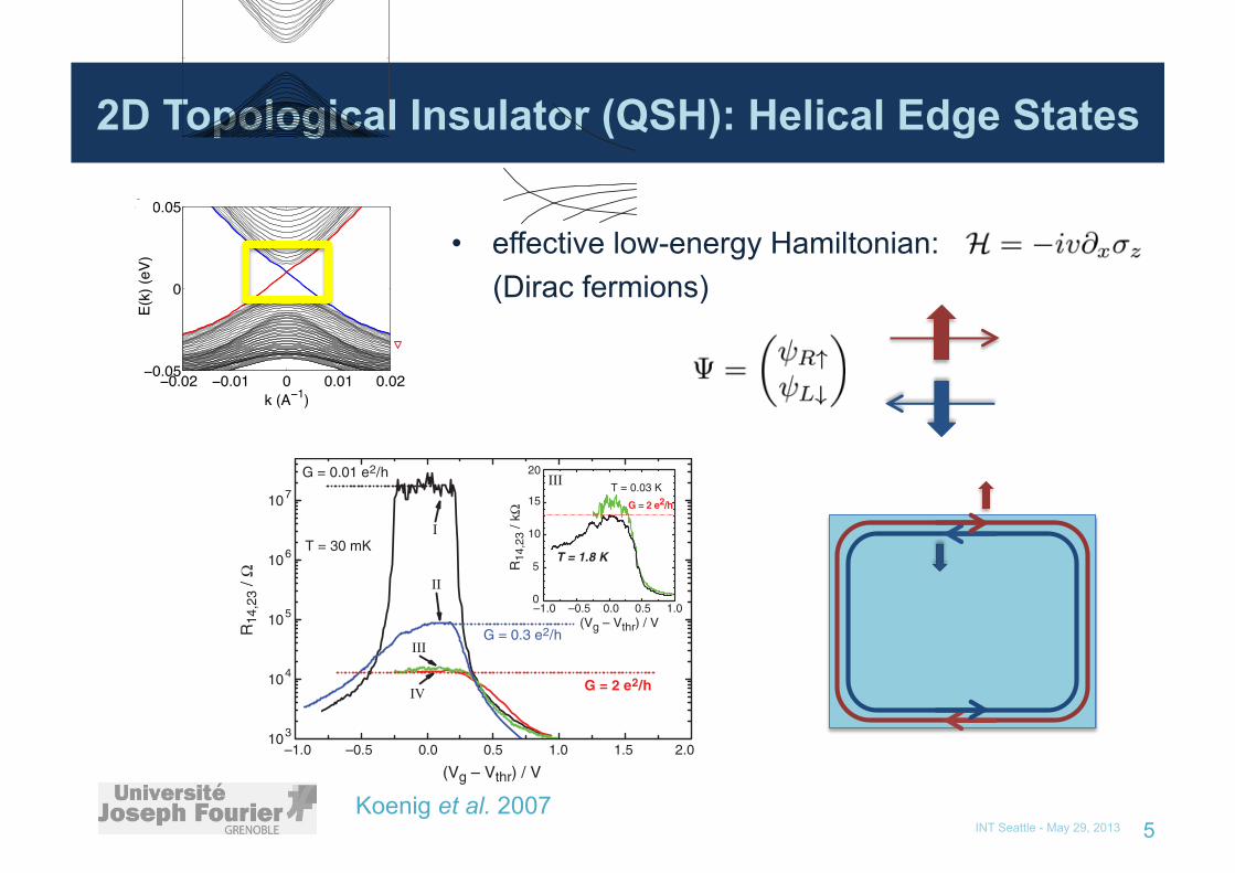
2D Topological Insulator (QSH): Helical Edge States
• effective low-energy Hamiltonian: (Dirac fermions)
INT Seattle - May 29, 2013 4
8
The coefficients a, b, c, d can be determined by imposing theopen boundary condition !(0) = 0. Together with the nor-malizability of the wave function in the region x > 0, theopen boundary condition leads to an existence condition forthe edge states: !"1,2 < 0 (c = d = 0) or !"1,2 > 0(a = b = 0), where ! stands for the real part. As seen fromEq. (15), these conditions can only be satisfied in the invertedregime when M/B > 0. Furthermore, one can show thatwhen A/B < 0, we have !"1,2 < 0, while when A/B > 0,we have!"1,2 > 0. Therefore, the wave function for the edgestates at the ! point is given by
!0(x) =
!
a"
e!1x " e!2x#
#+, A/B < 0;
c"
e!!1x " e!!2x#
#!, A/B > 0.(16)
The sign of A/B determines the spin polarization of the edgestates, which is key to determine the helicity of the DiracHamiltonian for the topological edge states. Another im-portant quantity characterizing the edge states is their decaylength, which is defined as lc = max
$
|!"1,2|!1%
.The effective edge model can be obtained by projecting the
bulk Hamiltonian onto the edge states "" and "# defined inEq. (11). This procedure leads to a 2 # 2 effective Hamil-tonian defined by H"#
edge(ky) = $""|&
H0 + H1
'
|"#%. Toleading order in ky , we arrive at the effective Hamiltonian forthe helical edge states:
Hedge = Aky$z . (17)
For HgTe QWs, we have A & 3.6 eV·A (Konig et al., 2008),and the Dirac velocity of the edge states is given by v =A/! & 5.5# 105 m/s.The analytical calculation above can be confirmed by exact
numerical diagonalization of the Hamiltonian (2) on a stripof finite width, which can also include the contribution ofthe %(k) term [Fig. 4]. The finite decay length of the heli-cal edge states into the bulk determines the amplitude for in-teredge tunneling (Hou et al., 2009; Strom and Johannesson,2009; Tanaka et al., 2009; Teo and Kane, 2009; Zhou et al.,2008; Zyuzin and Fiete, 2010).
C. Physical properties of the helical edge states
1. Topological protection of the helical edge states
From the explicit analytical solution of the BHZ model,there is a pair of helical edge states exponentially localizedat the edge, and described by the effective helical edge the-ory (17). In this context, the concept of “helical” edgestate (Wu et al., 2006) refers to the fact that states with op-posite spin counter-propagate at a given edge, as we see fromthe edge state dispersion relation shown in Fig. 4(b), or thereal space picture shown in Fig. 1(b). This is in sharp contrastto the “chiral” edge states in the QH state, where the edgestates propagate in one direction only, as shown in Fig. 1(a).
−0.02 −0.01 0 0.01 0.02−0.05
0
0.05
k (A−1)
E(k)
(eV)
−0.02 −0.01 0 0.01 0.02−0.05
0
0.05
k (A−1)E(
k) (e
V)
(a)
(b)
FIG. 4 Energy spectrum of the effective Hamiltonian (2) in a cylin-der geometry. In a thin QW, (a) there is a gap between conductionband and valence band. In a thick QW, (b) there are gapless edgestates on the left and right edge (red and blue lines, respectively).The dashed line stands for a typical value of the chemical potentialwithin the bulk gap. Adapted from Qi and Zhang, 2010.
In the QH effect, the chiral edge states can not be backscat-tered for sample widths larger than the decay length of theedge states. In the QSH effect, one may naturally ask whetherbackscattering of the helical edge states is possible. It turnsout that TR symmetry prevents the helical edge states frombackscattering. The absence of backscattering relies on thedestructive interference between all possible backscatteringpaths taken by the edge electrons.Before giving a semiclassical argument why this is so,
we first consider an analogy from daily experience. Mosteyeglasses and camera lenses have an antireflective coating[Fig. 5(a)], where light reflected from the top and bottom sur-faces interfere destructively, leading to no net reflection andthus perfect transmission. However, this effect is not robust,as it depends on a precise matching between the wavelengthof light and the thickness of the coating. Now we turn to thehelical edge states. If a nonmagnetic impurity is present nearthe edge, it can in principle cause backscattering of the heli-cal edge states due to SOC. However, just as for the reflec-tion of photons by a surface, an electron can be reflected bya nonmagnetic impurity, and different reflection paths inter-fere quantum-mechanically. A forward-moving electron withspin up on the QSH edge can make either a clockwise or acounterclockwise turn around the impurity [Fig. 5(b)]. Sinceonly spin down electrons can propagate backwards, the elec-tron spin has to rotate adiabatically, either by an angle of &or "&, i.e. into the opposite direction. Consequently, the two
Vacuum TI Vacuum Gap > 0 Gap < 0 Gap > 0
Position
Gap
2D Topological Insulator (QSH): Helical Edge States
• effective low-energy Hamiltonian: (Dirac fermions)
Koenig et al. 2007
INT Seattle - May 29, 2013 5
8
The coefficients a, b, c, d can be determined by imposing theopen boundary condition !(0) = 0. Together with the nor-malizability of the wave function in the region x > 0, theopen boundary condition leads to an existence condition forthe edge states: !"1,2 < 0 (c = d = 0) or !"1,2 > 0(a = b = 0), where ! stands for the real part. As seen fromEq. (15), these conditions can only be satisfied in the invertedregime when M/B > 0. Furthermore, one can show thatwhen A/B < 0, we have !"1,2 < 0, while when A/B > 0,we have!"1,2 > 0. Therefore, the wave function for the edgestates at the ! point is given by
!0(x) =
!
a"
e!1x " e!2x#
#+, A/B < 0;
c"
e!!1x " e!!2x#
#!, A/B > 0.(16)
The sign of A/B determines the spin polarization of the edgestates, which is key to determine the helicity of the DiracHamiltonian for the topological edge states. Another im-portant quantity characterizing the edge states is their decaylength, which is defined as lc = max
$
|!"1,2|!1%
.The effective edge model can be obtained by projecting the
bulk Hamiltonian onto the edge states "" and "# defined inEq. (11). This procedure leads to a 2 # 2 effective Hamil-tonian defined by H"#
edge(ky) = $""|&
H0 + H1
'
|"#%. Toleading order in ky , we arrive at the effective Hamiltonian forthe helical edge states:
Hedge = Aky$z . (17)
For HgTe QWs, we have A & 3.6 eV·A (Konig et al., 2008),and the Dirac velocity of the edge states is given by v =A/! & 5.5# 105 m/s.The analytical calculation above can be confirmed by exact
numerical diagonalization of the Hamiltonian (2) on a stripof finite width, which can also include the contribution ofthe %(k) term [Fig. 4]. The finite decay length of the heli-cal edge states into the bulk determines the amplitude for in-teredge tunneling (Hou et al., 2009; Strom and Johannesson,2009; Tanaka et al., 2009; Teo and Kane, 2009; Zhou et al.,2008; Zyuzin and Fiete, 2010).
C. Physical properties of the helical edge states
1. Topological protection of the helical edge states
From the explicit analytical solution of the BHZ model,there is a pair of helical edge states exponentially localizedat the edge, and described by the effective helical edge the-ory (17). In this context, the concept of “helical” edgestate (Wu et al., 2006) refers to the fact that states with op-posite spin counter-propagate at a given edge, as we see fromthe edge state dispersion relation shown in Fig. 4(b), or thereal space picture shown in Fig. 1(b). This is in sharp contrastto the “chiral” edge states in the QH state, where the edgestates propagate in one direction only, as shown in Fig. 1(a).
−0.02 −0.01 0 0.01 0.02−0.05
0
0.05
k (A−1)
E(k)
(eV)
−0.02 −0.01 0 0.01 0.02−0.05
0
0.05
k (A−1)E(
k) (e
V)
(a)
(b)
FIG. 4 Energy spectrum of the effective Hamiltonian (2) in a cylin-der geometry. In a thin QW, (a) there is a gap between conductionband and valence band. In a thick QW, (b) there are gapless edgestates on the left and right edge (red and blue lines, respectively).The dashed line stands for a typical value of the chemical potentialwithin the bulk gap. Adapted from Qi and Zhang, 2010.
In the QH effect, the chiral edge states can not be backscat-tered for sample widths larger than the decay length of theedge states. In the QSH effect, one may naturally ask whetherbackscattering of the helical edge states is possible. It turnsout that TR symmetry prevents the helical edge states frombackscattering. The absence of backscattering relies on thedestructive interference between all possible backscatteringpaths taken by the edge electrons.Before giving a semiclassical argument why this is so,
we first consider an analogy from daily experience. Mosteyeglasses and camera lenses have an antireflective coating[Fig. 5(a)], where light reflected from the top and bottom sur-faces interfere destructively, leading to no net reflection andthus perfect transmission. However, this effect is not robust,as it depends on a precise matching between the wavelengthof light and the thickness of the coating. Now we turn to thehelical edge states. If a nonmagnetic impurity is present nearthe edge, it can in principle cause backscattering of the heli-cal edge states due to SOC. However, just as for the reflec-tion of photons by a surface, an electron can be reflected bya nonmagnetic impurity, and different reflection paths inter-fere quantum-mechanically. A forward-moving electron withspin up on the QSH edge can make either a clockwise or acounterclockwise turn around the impurity [Fig. 5(b)]. Sinceonly spin down electrons can propagate backwards, the elec-tron spin has to rotate adiabatically, either by an angle of &or "&, i.e. into the opposite direction. Consequently, the two
Although the four-band Dirac model (Eq. 1)gives a simple qualitative understanding ofthis novel phase transition, we also performedmore realistic and self-consistent eight-bandk·p model calculations (13) for a 6.5-nm quan-tum well, with the fan chart of the Landaulevels displayed in Fig. 1B. The two anoma-lous Landau levels cross at a critical magneticfield Bc
!, which evidently depends on wellwidth. This implies that when a sample has itsFermi energy in the gap at zero magneticfield, this energy will always be crossed bythe two anomalous Landau levels, resulting ina QH plateau in-between the two crossingfields. Figure 3 summarizes the dependenceof Bc
! on well width d. The open red squaresare experimental data points that result fromfitting the eight-band k·p model to experi-mental data as in Fig. 1, while the filled redtriangles result solely from the k·p calcula-tion. For reference, the calculated gap ener-gies are also plotted in this graph as openblue circles. The band inversion is reflectedin the sign change of the gap. For relativelywide wells (d > 8.5 nm), the (inverted) gap
starts to decrease in magnitude. This is be-cause for these well widths, the band gap nolonger occurs between the E1 and HH1 lev-els, but rather between HH1 and HH2—thesecond confined hole-like level, as schemat-ically shown in the inset of Fig. 3 [see also(17)]. Also in this regime, a band crossing ofconductance- (HH1) and valence- (HH2) band–derived Landau levels occurs with increasingmagnetic field (13, 17, 18). Figure 3 clearlyillustrates the quantum phase transition thatoccurs as a function of d in the HgTe QWs:Only for d > dc does Bc
! exist, and at thesame time the energy gap is negative (i.e.,the band structure is inverted). The experimen-tal data allow for a quite accurate determi-nation of the critical thickness, yielding dc =6.3 ± 0.1 nm.
Zero-field edge channels and the QSHeffect. The actual existence of edge channelsin insulating inverted QWs is only revealedwhen studying smaller Hall bars [the typicalmobility of 105 cm2 V"1 s"1 in n-type materialimplies an elastic mean free path of lmfp #1 mm (19, 20)—and one may anticipate lower
mobilities in the nominally insulating regime].The pertinent data are shown in Fig. 4, whichplots the zero B-field four-terminal resistanceR14,23 $ V23/I14 as a function of normalized gatevoltage (Vthr is defined as the voltage for whichthe resistance is largest) for several devices thatare representative of the large number ofstructures we investigated. R14,23 is measuredwhile the Fermi level in the device is scannedthrough the gap. In the low-resistance regions atpositive Vg " Vthr, the sample is n-type; atnegative Vg " Vthr, the sample is p-type.
The black curve labeled I in Fig. 4 wasobtained from a medium-sized [(20.0 ! 13.3)mm2] device with a 5.5-nm QW and shows thebehavior we observe for all devices with anormal band structure: When the Fermi levelis in the gap, R14,23 increases strongly and isat least several tens of megohm (this is the de-tection limit of the lock-in equipment used inthe experiment). This clearly is the expectedbehavior for a conventional insulator. How-ever, for all devices containing an inverted QW,the resistance in the insulating regime remainsfinite. R14,23 plateaus at well below 100 kilohm(i.e., G14,23 = 0.3 e2/h) for the blue curvelabeled II, which is again for a (20.0 ! 13.3)mm2 device fabricated by optical lithography,but that contains a 7.3-nm-wide QW. For muchshorter samples (L = 1.0 mm, green and redcurves III and IV) fabricated from the samewafer, G14,23 actually reaches the predictedvalue close to 2e2/h, demonstrating the exis-tence of the QSH insulator state for invertedHgTe QW structures.
Figure 4 includes data on two devices withd = 7.3 nm, L = 1.0 mm. The green trace (III)is from a device with W = 1.0 mm, and the redtrace (IV) corresponds to a device with W =0.5 mm. Clearly, the residual resistance of thedevices does not depend on the width of thestructure, which indicates that the transportoccurs through edge channels (21). The tracesfor the d = 7.3 nm, L = 1.0 mm devices do notreach all the way into the p-region because theelectron-beam lithography needed to fabricatethe devices increases the intrinsic (Vg = 0 V)carrier concentration. In addition, fluctuationson the conductance plateaus in traces II, III,and IV are reproducible and do not stem from,e.g., electrical noise. Although all R14,23 tracesdiscussed so far were taken at the basetemperature (30 mK) of our dilution refriger-ator, the conductance plateaus are not limitedto this very-low-temperature regime. In theinset of Fig. 4, we reproduce the green 30-mKtrace III on a linear scale and compare it witha trace (in black) taken at 1.8 K from another(L ! W) = (1.0 ! 1.0) mm2 sample, which wasfabricated from the same wafer. In the fabrica-tion of this sample, we used a lower-illuminationdose in the e-beam lithography, resulting in abetter (but still not quite complete) coverage ofthe n-i-p transition. Clearly, in this furthersample, and at 1.8 K, the 2e2/h conductance
Fig. 3. Crossing field,Bc! (red triangles), andenergy gap, Eg (blueopen dots), as a func-tion of QW width dresulting from an eight-band k·p calculation.For well widths largerthan 6.3 nm, the QW isinverted and a mid-gapcrossing of Landau levelsderiving from the HH1conductance and E1 va-lence band occurs at fi-nite magnetic fields. Theexperimentally observedcrossing points are in-dicated by open redsquares. The inset showsthe energetic ordering of the QW subband structure as a function of QW width d. [See also (17)].
3 4 5 6 7 8 9 10 11 12
–40
–20
0
20
40
60
80
100
0
2
4
6
8
10
4 6 8 10 12 14–100
–50
0
50
100
150
200
HH4HH3HH2
HH1
E1E /
meV
d / nm
E2
Eg
/ meV
d / nm
normal inverted
Bc / T
Fig. 4. The longitudinal four-terminal resistance, R14,23, ofvarious normal (d = 5.5 nm)(I) and inverted (d = 7.3 nm)(II, III, and IV) QW structuresas a function of the gate volt-age measured for B = 0 T atT = 30 mK. The device sizesare (20.0 ! 13.3) mm2 fordevices I and II, (1.0 ! 1.0)mm2 for device III, and (1.0!0.5) mm2 for device IV. Theinset shows R14,23(Vg) of twosamples from the samewafer,having the same device size(III) at 30 mK (green) and1.8 K (black) on a linear scale.
–1.0 –0.5 0.0 0.5 1.0 1.5 2.0103
104
105
106
107
R14
,23
/ !
R14
,23
/ k!
G = 0.3 e2/h
G = 0.01 e2/h
T = 30 mK
–1.0 –0.5 0.0 0.5 1.00
5
10
15
20
G = 2 e2/h
G = 2 e2/h
T = 0.03 K
(Vg – Vthr) / V
(Vg – Vthr) / V
T = 1.8 K
www.sciencemag.org SCIENCE VOL 318 2 NOVEMBER 2007 769
RESEARCH ARTICLES
on
Janu
ary
10, 2
013
ww
w.s
cien
cem
ag.o
rgD
ownl
oade
d fro
m

1D Topological Superconductor: Majorana Fermions
• topological superconductor: 1D spinless p-wave • edge state = Majorana fermion
Oreg, Refael & von Oppen, PRL (2010) Lutchyn, Sau & Das Sarma, PRL (2010)
Alicea, Rep. Prog. Phys. (2012)
Kitaev, Phys. Usp. (2001)
Possible realizations: • 2D topological insulator (QSH) + conventional superconductor • nanowire with strong spin-orbit coupling & Zeeman field
+ conventional superconductor proximity effect → topological superconductivity
INT Seattle - May 29, 2013 6
(b) E
k
µ∆
Eso
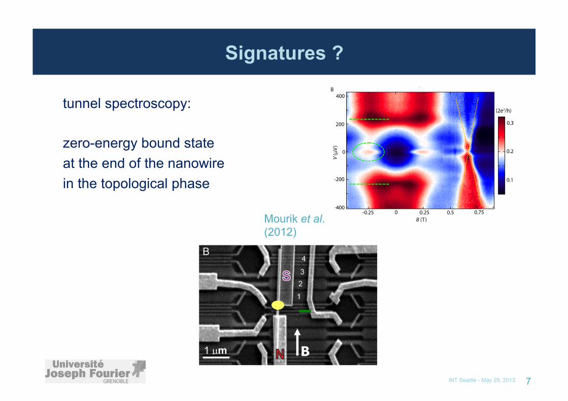
Signatures ?
tunnel spectroscopy: zero-energy bound state at the end of the nanowire in the topological phase
Mourik et al. (2012)
INT Seattle - May 29, 2013 7
!"#$$%&!!'''()*+,-*,./0(120!*1-$,-$!,/234!2,*,-$"!"56"7%2+3"6856"!"9/0,":"!"58(556;!)*+,-*,(5666:;8""
*1<,2,=" '+$#" )>%,2*1-=>*$12" +)" .>*#" 3,))" ,??,*$+<," =>," $1" ,??+*+,-$")*2,,-+-0("@#,"->.A,2"1?"1**>%+,=")>AA/-=)"+-"$#+)"%/2$"+)">-B-1'-C"A>$"+$"+)".1)$"3+B,34".>3$+D)>AA/-=("7)")#1'-"+-"?+0)("EF"/-="E55"1?"G!"H"',"=1"#/<,"$1"$>-,"0/$,"5"/-="$#,"$>--,3"A/22+,2"$1"$#,"2+0#$"2,0+.,"+-"12=,2"$1"1A),2<,"$#,"IJ9("
K,"#/<,".,/)>2,="+-"$1$/3"),<,2/3"#>-=2,="%/-,3)")',,%+-0"</2+1>)"0/$,)"1-"=+??,2,-$"=,<+*,)("L>2"./+-"1A),2</$+1-)"G!"H"/2,"G+H"IJ9",M+)$)"1<,2"/")>A)$/-$+/3"<13$/0,"2/-0,"?12",<,24"0/$,")$/2$+-0"?21."$#,"A/22+,2"0/$," >-$+3" 0/$," NC" G++H" '," */-" 1**/)+1-/334" )%3+$" $#," IJ9" +-" $'1" %,/B)"31*/$,=")4..,$2+*/334"/21>-="O,21C"/-="G+++H"',"*/-"-,<,2".1<,"$#,"%,/B"/'/4" ?21."O,21" $1" ?+-+$,"A+/)("P/$/" ),$)" )>*#"/)" $#1)," +-"Q+0)("6"/-=":"=,.1-)$2/$,"$#/$"$#,"IJ9"2,./+-)")$>*B"$1"O,21",-,204"1<,2"*1-)+=,2/A3,"*#/-0,)"+-"#"/-="0/$,"<13$/0,"$0("
Q+0>2,":P")#1')" $#," $,.%,2/$>2,"=,%,-=,-*,"1?" $#,"IJ9("K,"?+-="
$#/$"$#,"%,/B"=+)/%%,/2)"/$"/21>-="R:88".SC"%21<+=+-0"/"$#,2./3",-,204")*/3," 1?" %J&" R" :8" ,T(" @#," ?>33D'+=$#" /$" #/3?D./M+.>." /$" $#," 31',)$"$,.%,2/$>2,"+)"R68" ,TC"'#+*#"',"A,3+,<," +)"/"*1-),U>,-*,"1?" $#,2./3"A21/=,-+-0"/)":(VW%J&G;8".SH"X"5Y" ,T("
Z,M$"',"<,2+?4",M%3+*+$34"$#/$"/33"$#,"2,U>+2,="+-02,=+,-$)"+-"$#,"$#,1D2,$+*/3"[/\12/-/"%21%1)/3)" GQ+0("57H"/2," +-=,,=",)),-$+/3" ?12"1A),2<+-0"$#," IJ9(" K," #/<," /32,/=4" <,2+?+,=" $#/$" /" -1-O,21" #D?+,3=" +)" -,,=,=("Z1'C"',"$,)$"+?")%+-D12A+$"+-$,2/*$+1-"+)"*2>*+/3"?12"$#,"/A),-*,"12"%2,)D,-*,"1?" $#,"IJ9("@#,124" 2,U>+2,)" $#/$" $#,",M$,2-/3"#" #/)" /" *1.%1-,-$"%,2%,-=+*>3/2" $1"#)1("K,"#/<,".,/)>2,="/" ),*1-="=,<+*," +-"/"=+??,2,-$"),$>%"*1-$/+-+-0"/":P"<,*$12"./0-,$")>*#"$#/$"',"*/-")',,%"$#,"#"?+,3="+-"/2A+$2/24"=+2,*$+1-)("]-"Q+0("N"',")#1'"'(!'$"<,2)>)"$"'#+3,"</24+-0"$#,"/-03,"?12"/"*1-)$/-$"?+,3="./0-+$>=,("]-"Q+0("N7"$#,"%3/-,"1?"21$/$+1-"+)"/%%21M+./$,34",U>/3"$1"$#,"%3/-,"1?"$#,")>A)$2/$,("K,"*3,/234"1A),2<,"$#/$"$#,"IJ9"*1.,)"/-="01,)"'+$#"/-03,("@#,"IJ9"+)"*1.%3,$,34"/A),-$"/21>-=" !6C"'#+*#"$#,2,A4"',"=,=>*,"/)"$#,"=+2,*$+1-"1?"#)1("]-"Q+0("NJ"$#,"%3/-,"1?"21$/$+1-"+)"%,2%,-=+*>3/2"$1"#)1("]-=,,="',"1A),2<,"$#/$"$#,"IJ9"+)"-1'"%2,),-$"?12"/33"/-03,)C"A,*/>),"#"+)"-1'"/3'/4)"%,2%,-=+*>D3/2"$1"#)1("@#,),"1A),2</$+1-)"/2,"+-"?>33"/02,,.,-$"'+$#",M%,*$/$+1-)"?12"$#,")%+-D12A+$"=+2,*$+1-"+-"1>2")/.%3,)"G)*C+,)H("K,"#/<,"?>2$#,2"<,2+?+,="$#/$"$#+)"/-03,"=,%,-=,-*,"+)"-1$"/"2,)>3$"1?"$#,")%,*+?+*"./0-+$>=,"1?"#"12"/"</2+/$+1-"+-"-D?/*$12"G!"H("
7)"/"3/)$"*#,*B"',"#/<,"?/A2+*/$,="/-=".,/)>2,="/"=,<+*,"1?"+=,-$+D*/3"=,)+0-"A>$"'+$#"$#,")>%,2*1-=>*$12"2,%3/*,="A4"/"-12./3"7>"*1-$/*$"G+(,(C"/"ZDZKDZ"0,1.,$24H("]-"$#+)")/.%3,"',"#/<,"-1$"?1>-="/-4")+0-/D$>2,"1?"/"%,/B"$#/$")$+*B)"$1"O,21"A+/)"'#+3,"*#/-0+-0"A1$#"#"/-="$0"G!"H("
Fig. 3.!"#$%!&'($#)%!*%+%,*%,-%.! /A0!12!-'('3!+('$!'4!dI5dV!&%3676!V!#,*!&'($#)%!',!)#$%!1!#$!89:!;<!#,*!=>!;?.!@,A*3%%&! B'7,*! 6$#$%6! -3'66! $C3'7)C! D%3'! BE#6F! 4'3! %G#;+(%!,%#3!A:!H!/*'$$%*!(E,%60.!<C%!IJK!E6!&E6EB(%!43';!L8>!$'!M:!H!/#($C'7)C! E,! $CE6! -'('3! 6%$$E,)! E$! E6! ,'$! %N7#((O! &E6EB(%! %&%3OAPC%3%0.!Q+(E$!+%#R6!#3%!'B6%3&%*!E,!$C%!3#,)%!'4!9.:!$'!8>!H!/200.! S,! /B0!#,*! /C0!P%!-';+#3%!&'($#)%!6P%%+6!',!)#$%!T!4'3! >! #,*! 1>>!;<!PE$C! $C%! D%3'! BE#6! +%#R! #B6%,$! #,*! +3%A6%,$F! 3%6+%-$E&%(O.! <%;+%3#$73%! E6! :>!;?.! UV'$%! $C#$! E,! /W0!$C%!+%#R!%G$%,*6!#((!$C%!P#O!$'!L8>!H!/190.X!/D0!<%;+%3#$73%!*%+%,*%,-%.!dI5dV!&%3676!V!#$!8:>!;<.!<3#-%6!C#&%!#,!'44A6%$!4'3!-(#3E$O!/%G-%+$!4'3!$C%!('P%6$!$3#-%0.!<3#-%6!#3%!$#R%,!#$!*E44%3%,$! $%;+%3#$73%6! /43';!B'$$';! $'! $'+Y!=>F!8>>F! 81:F!8:>F!89:F!1>>F!11:F!1:>F!#,*!Z>>!;?0.!dI5dV!'7$6E*%!IJK!#$!V![!8>>! %H!E6!>.81!\!>.>8]1e15h!4'3!#((!$%;+%3#$73%6.!@!47((APE*$C! #$! C#(4A;#GE;7;!'4! 1>! %H! E6!;%#673%*! B%$P%%,! #3A3'P6.!@((!*#$#!E,!$CE6!4E)73%!#3%!43';!*%&E-%!8.
Fig. 2.! ^#),%$E-! 4E%(*! *%+%,*%,$! 6+%-$3'6-'+O.! /A0! dI5dV!&%3676!V!#$!9>!;?!$#R%,!#$!*E44%3%,$!BA4E%(*6!/43';!>! $'!T_>!;<!E,!8>!;<!6$%+6`!$3#-%6!#3%!'446%$!4'3!-(#3E$OF!%G-%+$!4'3!$C%!('P%6$! $3#-%!#$!B! [!>0.!2#$#! 43';!*%&E-%! 8.! /B0!W'('3! 6-#(%!+('$!'4!dI5dV!&%3676!V!#,*!B.!<C%!D%3'ABE#6!+%#R!E6!CE)C(E)C$A%*!BO!#!*#6C%*!'&#(.!2#6C%*!(E,%6!E,*E-#$%!$C%!)#+!%*)%6.!@$!M>.=! <! #! ,',A^#a'3#,#! 6$#$%! E6! -3'66E,)! D%3'! BE#6! PE$C! #!6('+%!%N7#(! $'!~Z!;%H5<! /E,*E-#$%*!BO!6('+%*!*'$$%*! (E,%60.!<3#-%6!E,!/@0!#3%!%G$3#-$%*!43';!/J0.
on
April
16,
201
2w
ww
.sci
ence
mag
.org
Dow
nloa
ded
from
!"#$$%&!!'''()*+,-*,./0(120!*1-$,-$!,/234!2,*,-$"!"56"7%2+3"6856"!"9/0,"6"!"58(556:!)*+,-*,(5666;:8""
$#21<0#1<$"$#,"0/%"2,0+1-("=4..,$2+*"2,)1-/-*,)"3+>,34"12+0+-/$,"?21."7-@2,,A"B1<-@")$/$,)"C!"D#!!ED"'#,2,/)"-1-F2,)1-/-$"*<22,-$" +-@+*/$,)"$#/$"$#,"%21G+.+$4"0/%"#/)"-1$"?<334"@,A,31%,@"C!$E("
H+0<2," 6" )<../2+I,)" 1<2" ./+-" 2,)<3$(" H+0<2," 67" )#1')" /" ),$" 1?"%&!%'"A,2)<)"'" $2/*,)"$/>,-"/$"+-*2,/)+-0"(F?+,3@)"+-"58".J")$,%)"?21."I,21" C31',)$" $2/*,E" $1" KL8".J" C$1%" $2/*,ED" 1??),$" ?12" *3/2+$4("M,"/0/+-"1B),2A,"$#,"0/%",@0,)"/$"N6O8" ,P("M#,-"',"/%%34"/"(F?+,3@"B,$',,-"Q588"/-@"QK88".J"/31-0"$#,"-/-1'+2,"/G+)"',"1B),2A,"/"%,/>"/$"'"R"8("J#,"%,/>"#/)"/-"/.%3+$<@,"<%"$1"Q8(8OS6)!!*"/-@"+)"*3,/234"@+)*,2-+B3,"?21."$#,"B/*>021<-@"*1-@<*$/-*,("7B1A,"QK88".J"',"1B),2A,"/"%/+2"1?"%,/>)("J#,"*1312"%/-,3"+-"H+0("6T"%21A+@,)"/-"1A,2A+,'"1?")$/$,)"/-@"0/%)"+-"$#,"%3/-,"1?",-,204"/-@"(F?+,3@"?21."U8(O"$1"5"J("J#,"1B),2A,@")4..,$24" /21<-@"(" R" 8" +)" $4%+*/3" ?12" /33" 1<2" @/$/" ),$)D" @,.1-)$2/$+-0"2,%21@<*+B+3+$4"/-@"$#,"/B),-*,"1?"#4)$,2,)+)("M,"+-@+*/$,"$#,"0/%",@0,)"'+$#"#12+I1-$/3"@/)#,@"3+-,)"C#+0#3+0#$,@"1-34"?12"("V"8E("7"%/+2"1?"2,)F1-/-*,)"*21)),)"I,21",-,204"/$"Q8(:O"J"'+$#"/")31%,"1?"12@,2"+W"C#+0#F3+0#$,@"B4"@1$$,@"3+-,)E("M,"#/A,"?1331',@"$#,),"2,)1-/-*,)"<%"$1"#+0#"B+/)"A13$/0,)"+-"C!,E"/-@"+@,-$+?+,@"$#,."/)"7-@2,,A")$/$,)"B1<-@"'+$#+-"$#," 0/%" 1?" $#," B<3>D"XBJ+X" )<%,2*1-@<*$+-0" ,3,*$21@,)" CQ6".,PE(" T4"*1-$2/)$D" $#,"I,21FB+/)"%,/>")$+*>)" $1"I,21",-,204"1A,2"/" 2/-0,"1?" ("Q";88".J"*,-$,2,@"/21<-@"Q6O8".J("70/+-"/$"QK88".J"',"1B),2A," $'1"%,/>)"31*/$,@"/$")4..,$2+*D"?+-+$,"B+/),)("
Y-" 12@,2" $1" +@,-$+?4" $#," 12+0+-" 1?" $#,)," I,21FB+/)" %,/>)" CWT9E" ',"-,,@" $1" *1-)+@,2" A/2+1<)" 1%$+1-)D" +-*3<@+-0" $#,"Z1-@1" ,??,*$D"7-@2,,A"B1<-@")$/$,)D"',/>"/-$+31*/3+I/$+1-"/-@"2,?3,*$+1-3,))"$<--,3+-0D"A,2)<)"/"*1-[,*$<2,"1?"\/[12/-/"B1<-@")$/$,)("WT9)"@<,"$1"$#,"Z1-@1",??,*$"C!-E"12" 7-@2,,A" )$/$,)" B1<-@" $1" )F'/A," )<%,2*1-@<*$12)" C!.E" */-" 1**<2" /$"?+-+$,"(("]1',A,2D"'#,-"*#/-0+-0"("$#,),"%,/>)"$#,-")%3+$"/-@".1A,"$1"?+-+$," ,-,204("7"Z1-@1" 2,)1-/-*,".1A,)"'+$#" $'+*,"+I" C!-ED"'#+*#" +)",/)4"$1"@+).+))"/)"$#,"12+0+-"?12"1<2"I,21FB+/)"%,/>"B,*/<),"1?"$#,"3/20,"/F?/*$12"+-"Y-=B("CX1$,"$#/$",A,-"/"Z1-@1",??,*$"?21."/-"+.%<2+$4"'+$#"/#0"6"'1<3@"B,"@+)*,2-+B3,(E"^,?3,*$+1-3,))"$<--,3+-0"+)"/-",-#/-*,.,-$"1?"7-@2,,A" 2,?3,*$+1-"B4" $+.,F2,A,2),@"%/$#)" +-"/"@+??<)+A,"-12./3" 2,0+1-"C!1E("7)"+-"$#,"*/),"1?"',/>"/-$+31*/3+I/$+1-D"$#,"2,)<3$+-0"WT9"+)"./G+F./3"/$"("R"8"/-@"@+)/%%,/2)"'#,-"("+)"+-*2,/),@D"),,"/3)1"C!,E("M,"$#<)"*1-*3<@,"$#/$"$#,"/B1A,"1%$+1-)"?12"/"WT9"@1"-1$"%21A+@,"-/$<2/3",G%3/F-/$+1-)" ?12"1<2"1B),2A/$+1-)("M,"/2,"-1$"/'/2,"1?" /-4".,*#/-+)." $#/$"
*1<3@",G%3/+-"1<2"1B),2A/$+1-)D"B,)+@,)"$#,"*1-[,*$<2,"1?"/"\/[12/-/("J1" ?<2$#,2" +-A,)$+0/$," $#," I,21FB+/)-,))" 1?" 1<2" %,/>D" '," .,/)<2,"
0/$,"A13$/0,"@,%,-@,-*,)("H+0<2,";7")#1')"/"*1312"%/-,3"'+$#"A13$/0,")',,%)"1-"0/$,"6("J#,"./+-"1B),2A/$+1-"+)"$#,"1**<22,-*,"1?"$'1"1%%1F)+$," $4%,)" 1?" B,#/A+12(" H+2)$D"'," 1B),2A," %,/>)" +-" $#," @,-)+$4" 1?" )$/$,)"$#/$" *#/-0,"'+$#" ,-,204"'#,-" *#/-0+-0" 0/$," A13$/0," C,(0(D" #+0#3+0#$,@"'+$#" @1$$,@" 3+-,)ED" $#,)," /2," $#," )/.," 2,)1-/-*,)" /)" )#1'-" +-" H+0(" 6T"/-@"/-/34I,@"+-"C!,E("J#,"),*1-@"1B),2A/$+1-"+)"$#/$"$#,"WT9"?21."H+0("6D"'#+*#"',"$/>,"/$"5_O".JD"2,./+-)")$<*>"$1"I,21"B+/)"'#+3,"*#/-0+-0"$#," 0/$," A13$/0," 1A,2" /" 2/-0," 1?" ),A,2/3" A13$)("`3,/234D" 1<2" 0/$,)"'12>")+-*,"$#,4"*#/-0,"$#,"7-@2,,A"B1<-@")$/$,)"B4"Q8(6".,P"%,2"P13$"1-"$#,"0/$,("9/-,3)"CTE"/-@"C`E"<-@,2)*12,"$#+)"1B),2A/$+1-"'+$#"A13$/0,")',,%)"1-"/"@+??,2,-$"0/$,D"-<.B,2"K("CTE")#1')"$#/$"/$"I,21"./0-,$+*"?+,3@"-1"WT9" +)" 1B),2A,@(" 7$" 688" .J" $#," WT9" B,*1.,)" /0/+-" A+)+B3," +-" C`E("`1.%/2+-0"$#,",??,*$"1?"0/$,)"6"/-@"KD"',"1B),2A,"$#/$"-,+$#,2".1A,)"$#,"WT9"/'/4"?21."I,21("
Y-+$+/334D"\/[12/-/"?,2.+1-)"',2,"%2,@+*$,@"+-")+-03,F)<BB/-@D"1-,F@+.,-)+1-/3"'+2,)"C2D#3ED"B<$"?<2$#,2"'12>",G$,-@,@"$#,),"%2,@+*$+1-)"$1".<3$+F)<BB/-@"'+2,)"C!45$,E("Y-"$#,"-/-1'+2,"),*$+1-"$#/$"+)"<-*1A,2,@"'," */-"0/$," $<-," $#,"-<.B,2"1?" 1**<%+,@" )<BB/-@)" ?21."8" $1"QK"'+$#")<BB/-@"),%/2/$+1-)"1?"),A,2/3".,P("a/$,"$<-+-0"+-"$#,"-/-1'+2,"),*$+1-"
Fig. 1.! "A#!$%&'()*! +,! &-*+.*&(/0'! 1.+1+20'23! "4+1#! 5+)/*1&%0'!6*7(/*!'08+%&!9(&-!0!2*:(/+)6%/&();!)0)+9(.*!()!1.+<(:(&8!&+!0)!2=907*!2%1*./+)6%/&+.3!>)!*<&*.)0'!B=,(*'6!(2!0'(;)*6!10.0''*'!&+!&-*! 9(.*3! 4-*!?02-@0! 21()=+.@(&! ()&*.0/&(+)! (2! ()6(/0&*6! 02! 0)!*,,*/&(7*!:0;)*&(/!,(*'6A!B2+A!1+()&();!1*.1*)6(/%'0.!&+!&-*!)0)=+9(.*3! 4-*! .*6! 2&0.2! ()6(/0&*! &-*! *<1*/&*6! '+/0&(+)2! +,! 0!B0C+.0)0!10(.3!"D+&&+:#!E)*.;8A!EA!7*.2%2!:+:*)&%:A!kA!,+.!0!FG! 9(.*! 9(&-! ?02-@0! 21()=+.@(&! ()&*.0/&(+)A! 9-(/-! 2-(,&2! &-*!21()=6+9)!@0)6!"@'%*#!&+!&-*!'*,&!0)6!21()=%1!@0)6!".*6#!&+!&-*!.(;-&3!D'%*!0)6!.*6!10.0@+'0!0.*!,+.!B!H!I3!D'0/J!/%.7*2!0.*!,+.!B! !IA!(''%2&.0&();!&-*!,+.:0&(+)!+,!0!;01!)*0.!k!H!I!+,!2(K*!g DB3!" !(2!&-*!L*.:(!*)*.;8!9(&-! !H!I!6*,()*6!0&!/.+22();!+,!10.0@+='02! 0&! k! H! I#3! 4-*! 2%1*./+)6%/&+.! ()6%/*2! 10(.();! @*&9**)!2&0&*2!+,!+11+2(&*!:+:*)&%:!0)6!+11+2(&*!21()!/.*0&();!0!;01!+,! 2(K*! 3! "B#! M:1'*:*)&*6! 7*.2(+)! +,! &-*+.*&(/0'! 1.+1+20'23!N/0))();!*'*/&.+)!:(/.+2/+1*!(:0;*!+,!&-*!6*7(/*!9(&-!)+.:0'!"O#!0)6! 2%1*./+)6%/&();! "N#! /+)&0/&23!4-*!N=/+)&0/&! +)'8! /+=7*.2!&-*!.(;-&!10.&!+,!&-*!)0)+9(.*3!4-*!%)6*.'8();!;0&*2A!)%:=@*.*6! F! &+! PA! 0.*! /+7*.*6! 9(&-! 0! 6(*'*/&.(/3! QO+&*! &-0&! ;0&*! F!/+))*/&2!&9+!;0&*2!0)6!;0&*!P!/+))*/&2!,+%.!)0..+9!;0&*2R!2**!"5#3S! "C#! "4+1#!N/-*:0&(/! +,! +%.! 6*7(/*3! "G+9)#! (''%2&.0&(+)! +,!*)*.;8!2&0&*23!T.**)!()6(/0&*2!&-*!&%))*'!@0..(*.!2*10.0&();!&-*!)+.:0'! 10.&! +,! &-*! )0)+9(.*! +)! &-*! '*,&! ,.+:! &-*! 9(.*! 2*/&(+)!9(&-!()6%/*6!2%1*./+)6%/&();!;01A! 3!QM)!"D#!&-*!@0..(*.!;0&*!(2!0'2+!:0.J*6!;.**)3S!>)!*<&*.)0'!7+'&0;*A!VA!011'(*6!@*&9**)!O!0)6!N!6.+12!0/.+22!&-*!&%))*'!@0..(*.3!?*6!2&0.2!0;0()!()6(/0&*!&-*! (6*0'(K*6! '+/0&(+)2! +,! &-*! B0C+.0)0! 10(.3! $)'8! &-*! '*,&!B0C+.0)0!(2!1.+@*6!()!&-(2!*<1*.(:*)&3!"D#!E<0:1'*!+,!6(,,*.*)=&(0'!/+)6%/&0)/*A!dIUdVA!7*.2%2!V!0&!B!H!I!0)6!VW!:XA!2*.7();!02!0!21*/&.+2/+1(/!:*02%.*:*)&!+)!&-*!6*)2(&8!+,!2&0&*2!()!&-*!)0)+9(.*!.*;(+)!@*'+9!&-*!2%1*./+)6%/&+.3!G0&0!,.+:!6*7(/*!F3!4-*!&9+!'0.;*!1*0J2A!2*10.0&*6!@8!Y A!/+..*21+)6!&+!&-*!Z%02(=10.&(/'*! 2();%'0.(&(*2! 0@+7*! &-*! ()6%/*6! ;013! 49+! 2:0''*.!2%@;01! 1*0J2A! ()6(/0&*6! @8! 0..+92A! '(J*'8! /+..*21+)6! &+! >)=6.**7!@+%)6!2&0&*2!'+/0&*6!28::*&.(/0''8!0.+%)6!K*.+!*)*.;83!B*02%.*:*)&2! 0.*! 1*.,+.:*6! ()! 6('%&(+)! .*,.(;*.0&+.2! %2();!2&0)60.6! '+9=,.*Z%*)/8! '+/J=()! &*/-)(Z%*! ",.*Z%*)/8! [[! \KA!*</(&0&(+)!]! ^#! ()! &-*! ,+%.=&*.:()0'! "6*7(/*2!F!0)6!]#!+.! &9+=&*.:()0'!"6*7(/*!Y#!/%..*)&=7+'&0;*!;*+:*&.83
on
April
16,
201
2w
ww
.sci
ence
mag
.org
Dow
nloa
ded
from

2D Topological Insulator
Fractional AC Josephson Effect ? – Setup
INT Seattle - May 29, 2013 8
Superconductor Superconductor
V

Fractional AC Josephson Effect ? – Setup
INT Seattle - May 29, 2013 9
Superconductor Superconductor
V

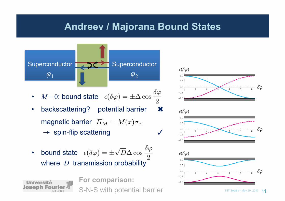
Andreev / Majorana Bound States
Hamiltonian:
INT Seattle - May 29, 2013 10
!0.5 0.5x!L
""x#
!0.5 0.5x!L
""x#
!0.5 0.5x!L
M"x#
Superconductor
φ1
Superconductor
φ2
1 2 3 4 5 6 !"
#1.0
#0.5
0.0
0.5
1.0
$!!""1 2 3 4 5 6 !"
#1.0
#0.5
0.0
0.5
1.0
$!!""
Andreev / Majorana Bound States
• M = 0: bound state
• backscattering? potential barrier
magnetic barrier → spin-flip scattering
• bound state where D transmission probability
For comparison: S-N-S with potential barrier INT Seattle - May 29, 2013 11
Superconductor
φ1
Superconductor
φ2
1 2 3 4 5 6 !"
#1.0
#0.5
0.0
0.5
1.0
$!!""
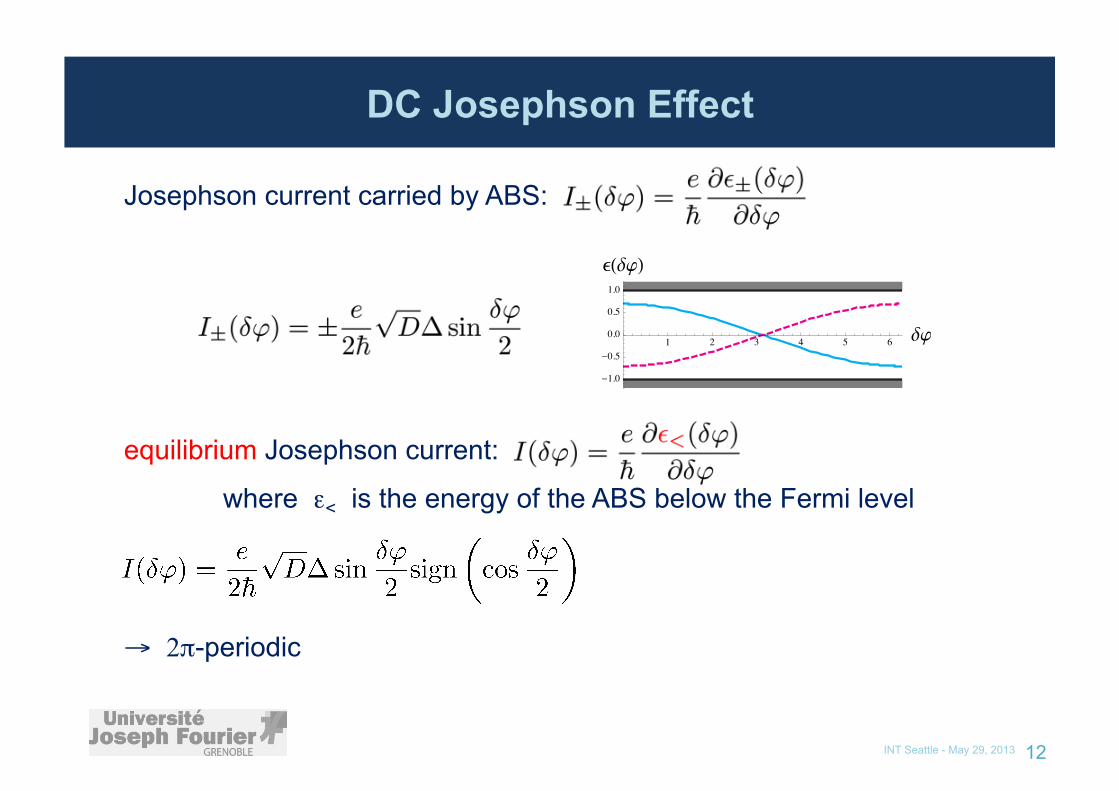
Josephson current carried by ABS:
equilibrium Josephson current:
where ε< is the energy of the ABS below the Fermi level
→ 2π-periodic
1 2 3 4 5 6 !"
#1.0
#0.5
0.0
0.5
1.0
$!!""
DC Josephson Effect
INT Seattle - May 29, 2013 12

Josephson current carried by ABS:
non-equilibrium Josephson current: δφ → 2eVdct
in the absence of inelastic processes • fractional Josephson effect at frequency eVdc = ωJ/2? • only even Shapiro steps?
for eVdc = kΩ (instead of 2eVdc = kΩ in S-N-S)
1 2 3 4 5 6 !"
#1.0
#0.5
0.0
0.5
1.0
$!!""
DC Josephson Effect
INT Seattle - May 29, 2013 13 Kitaev, Ann. Phys. (2003) Fu & Kane, PRB (2009)

Outline
• Andreev Bound States: S-N-S vs S-TI-S Josephson Junctions Fractional AC Josephson effect? • Effective Model: Bound State Dynamics
– Characteristic Time Scales – Average current & Noise
• Conclusions I
• Scattering Theory – Noise: comparison with the effective model – Additional signatures → MAR features
• Conclusions II
INT Seattle - May 29, 2013 14
NOTE: δϕ = ϕ = χ V = Vdc
Main Result
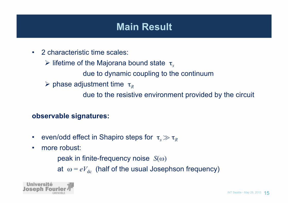
• 2 characteristic time scales: Ø lifetime of the Majorana bound state τs
due to dynamic coupling to the continuum Ø phase adjustment time τR
due to the resistive environment provided by the circuit observable signatures: • even/odd effect in Shapiro steps for τs À τR • more robust:
peak in finite-frequency noise S(ω) at ω = eVdc (half of the usual Josephson frequency)
INT Seattle - May 29, 2013 15
Effective Model
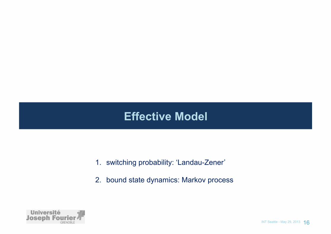
INT Seattle - May 29, 2013 16
1. switching probability: ‘Landau-Zener’
2. bound state dynamics: Markov process
2 ! 4 ! 6 ! 8 ! 10 ! 12 ! 14 ! 16 ! 18 ! 20 ! 22 ! 24 ! 26 ! 28 ! 30 !
Switching Probability: ‘Landau-Zener’
INT Seattle - May 29, 2013 17
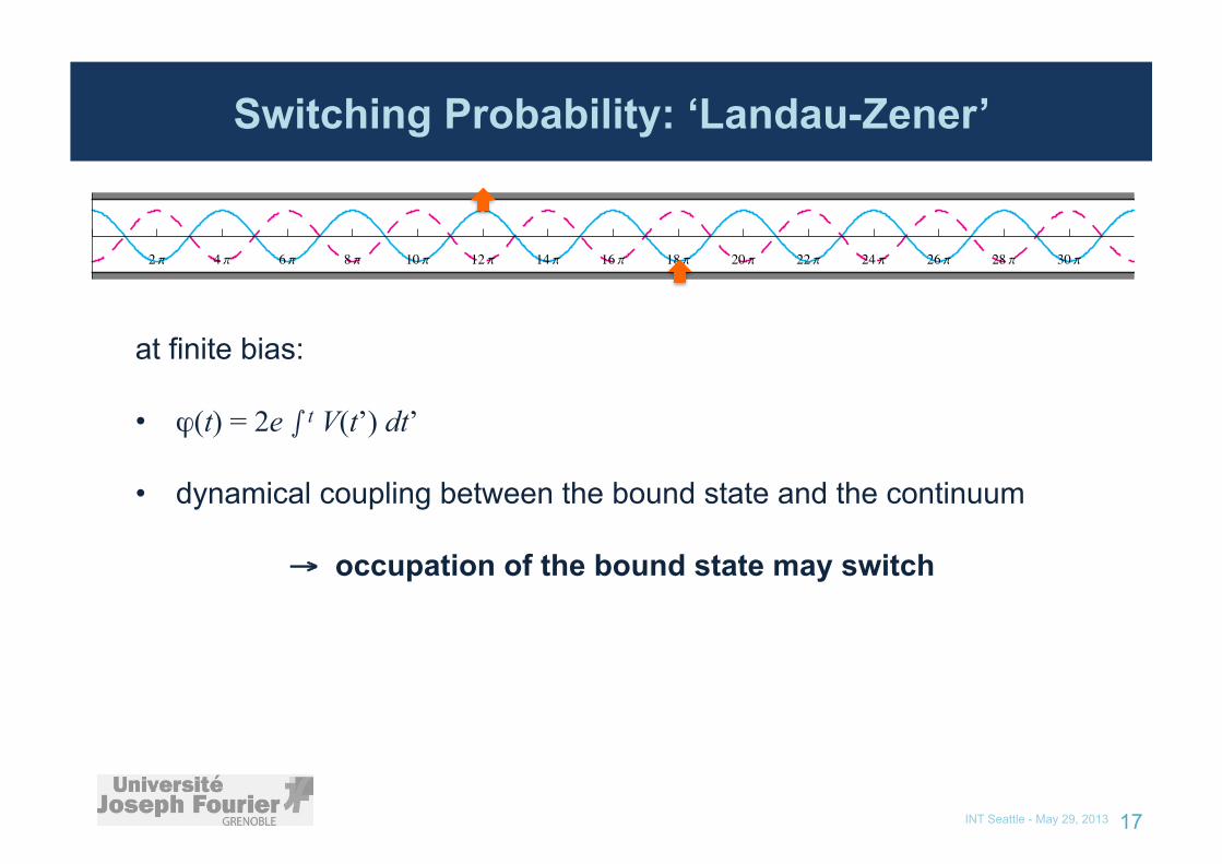
at finite bias: • ϕ(t) = 2e s t V(t’) dt’
• dynamical coupling between the bound state and the continuum
→ occupation of the bound state may switch

!2 " 2 " #!t"!1
1
$!#"#%
2 ! 4 ! 6 ! 8 ! 10 ! 12 ! 14 ! 16 ! 18 ! 20 ! 22 ! 24 ! 26 ! 28 ! 30 !
Switching Probability: ‘Landau-Zener’
INT Seattle - May 29, 2013 18
Hamiltonian : consider weak backscattering: R = 1–D ¿ 1
where R ~ (ML/v)2
!0.5 0.5x!L
""x#
!0.5 0.5x!L
""x#
!0.5 0.5x!L
M"x#

consider only states with energy near Δ:
ϕ ¿ 1 vp ¿ Δ
apply unitary transformation & diagonalize particle-hole space →
bound state similar to Shiba state created by a magnetic impurity in a superconductor
Shiba 1968, Rusinov 1969
Switching Probability at R ¿ 1
INT Seattle - May 29, 2013 19
!2 " 2 " #!t"!1
1
$!#"#%
+

+ time-dependent phase: ϕ = 2eVdc t use adiabatic basis
two-band version of transition from discrete state to continuum Demkov-Osherov (1967)
switching probability
Switching Probability at R ¿ 1
INT Seattle - May 29, 2013 20
! 3 "10!"5! "10 0 "
10"5
3 "10
#!t"0.8
0.9
1
1.1
$!#"#%
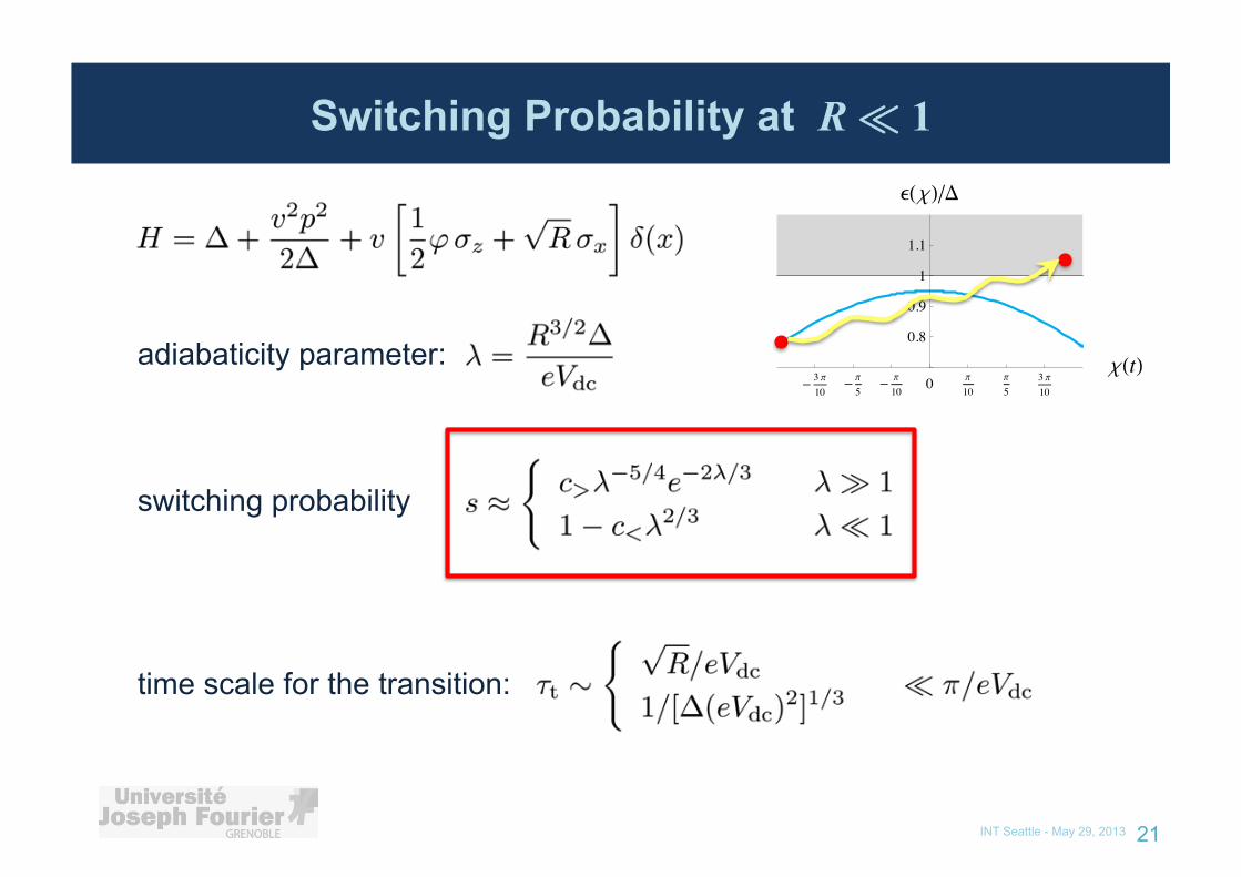
adiabaticity parameter: switching probability time scale for the transition:
Switching Probability at R ¿ 1
INT Seattle - May 29, 2013 21
! 3 "10!"5! "10 0 "
10"5
3 "10
#!t"0.8
0.9
1
1.1
$!#"#%

M. Houzet, JSM, D.M. Badiane & L.I. Glazman, arXiv:1303.4909
Switching Probability at R ¿ 1
INT Seattle - May 29, 2013 22
s 1 1.05 Λ23
s 0.93 Λ54 e2 Λ3
0 1 2 3 4 50.0
0.2
0.4
0.6
0.8
1.0
ΛR32eVdc
s

5 10 15!!t"#2"
I!t" 5 10 15!!t"#2"
#!t" 5 10 15!!t"#2"0
n!t"
Bound State Dynamics: Markov Process
INT Seattle - May 29, 2013 23
2 ! 4 ! 6 ! 8 ! 10 ! 12 ! 14 ! 16 ! 18 ! 20 ! 22 ! 24 ! 26 ! 28 ! 30 !

P probability of fermionic state to be occupied Q = 1 – P probability of fermionic state to be empty
s switching probability per half-period current: where
similar models have been used for Landau-Zener transitions near avoided crossings in conventional junctions Averin et al. 1995, Pikulin et al. 2011, Sau et al. 2012 …
Bound State Dynamics: Markov Process
INT Seattle - May 29, 2013 24
4 ! 6 ! "!t"4n¼ (4n+2)¼
1– s
s 1– s
s
Realistic Circuit: Time Scales
INT Seattle - May 29, 2013 25
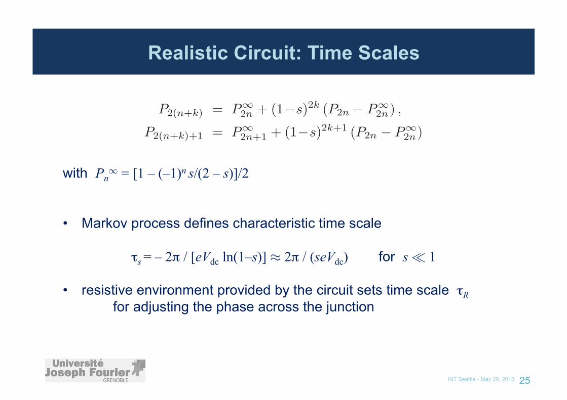
with Pn1 = [1 – (–1)n s/(2 – s)]/2
• Markov process defines characteristic time scale
τs = – 2π / [eVdc ln(1–s)] ¼ 2π / (seVdc) for s ¿ 1 • resistive environment provided by the circuit sets time scale τR
for adjusting the phase across the junction
3
!
!
!
!
!
!
!
!
!!!!!!!!!!!!!!!!!!!!!!!!!!!!!!!!!!!!!!!!!!!
!
!
!
!
!
""
"
"
"
"
"
s! 1 " 1.05 #2!3
s! 0.93 #"5!4 e"2 #!3
0 1 2 3 4 50.0
0.2
0.4
0.6
0.8
1.0
#$R3!2%!"eVdc#
s
FIG. 1: Switching probability s as a function of the adia-baticity parameter !. Dots: s found from a numerical solu-tion of the Schrodinger equation with Hamiltonian (3). Lines:asymptotic expressions for s, see text. Squares: s extractedfrom the “brute-force”evaluation of the noise spectrum bysolving numerically the problem of multiple Andreev reflec-tions [13] and fitting the result by Eq. (14), see [16] for details.
through s =!
p! |cp!(!)|2, using the initial conditionscA("!) = 1 and cp!("!) = 0. At ! # 1, using
cp!(t) $ i"(t)%#p!(t)| "H
"#(t) |#A(t)&$p! " $A(t)
e!i! t ds [$p!!$A(s)] ,
(7)the amplitudes cp!(!) are expressed through integralsthat may be evaluated by a saddle point method. Weobtain s ' 0.93!!5/4e!2%/3. Furthermore, we can iden-tify the time scale over which the transition happens,%t (
)R/(eVdc).
At arbitrary !, the switching probability can beobtained numerically by discretizing Eq. (3) on atight-binding lattice and solving the correspondingSchrodinger equation numerically. The result, togetherwith the asymptotes obtained above, is shown in Fig. 1.Using the fact that the transition time %t is much
shorter than the Josephson oscillation period, %t *&/(eVdc), we may now write an e!ective discrete Markovmodel for the bound state dynamics, cf. Fig. 2. Usinga discrete time evolution we assume that if the state isfilled, at phase "2n = 4n&, there is a probability s of theparticle to escape from the bound state to the continuum,whereas if the state is empty, at time "2n+1 = (4n+2)&,there is a probability s of a particle from the continuumfilling the bound state. Thus,
"
P2n+1
Q2n+1
#
=
"
1 s0 1" s
#"
P2n
Q2n
#
, (8a)
"
P2n
Q2n
#
=
"
1" s 0s 1
#"
P2n!1
Q2n!1
#
. (8b)
Here Pn is the probability for the state to be occupied,and Qn = 1 " Pn is the probability for the state to beempty at phases "n < "(t) < "n+1, corresponding ton = Int ["(t)/(2&)]. Solving these equations iteratively,
(a) 5 10 15eVdc t ! &0
n"t#
(b)5 10 15
eVdc t ! &
'"t#
(c)5 10 15
eVdc t ! &
I"t#
FIG. 2: Schematic view of the switching processes due to thecoupling with the continuum: (a) occupation n of the boundstate, (b) energy " of the system, and (c) Josephson currentI as a function of time t under dc bias voltage Vdc.
we obtain
P2(n+k) = P"2n + (1"s)2k (P2n " P"
2n) , (9a)
P2(n+k)+1 = P"2n+1 + (1"s)2k+1 (P2n " P"
2n). (9b)
The long-time probabilities at k # "1/ ln(1 " s), cor-responding to t # %s = "2&/[eVdc ln(1 " s)], are 4&-periodic and independent of the initial state: P"
n =[1" ("1)ns/(2" s)]/2.In order to determine the transport properties of the
junction, the switching time %s has to be compared toother characteristic time scales of the system. In par-ticular, if the junction is embedded into a circuit witha resistance R in series, the phase di!erence across thejunction may adjust over a typical time scale %R + R!1.If %s # %R, switching may be neglected (i.e., the
current may be obtained using the initial occupationsP0/Q0). Computing the dc current in the presence of anapplied voltage V (t) = Vdc + Vac cos("t) with Vac * Vdc
then yields the even-odd e!ect discussed in Refs. [8–10].Namely, taking into account a finite resistance R, theaverage current reads
Idc =$
k
'Vk
R
%
&
'
1" (
(
1""
RIk'Vk
#2)
*
1""
RIk'Vk
#2+
,
-
,
(10)where Ik = IJ |Jk())| is the height of the Shapiro stepat eVdc = k" and 'Vk = Vdc " k"/e. Here Jk are theBessel functions and ) = eVac/". The characteristic
time scale may be identified as [15, 16] % (k)R = 1/(eRIk)at eVdc ( k".A small resistance satisfying the relation RIJ * " is
advantageous for the resolution of Shapiro steps. Fur-thermore, long switching times require s * 1. Inthe small-s regime, the time scale %s decreases asexp[2R3/2#/(3k")] with increasing k. On the otherhand, at small ac perturbation, ) * 1, the time scale
% (k)R increases exponentially with k. The crossover from
RSJ Model
INT Seattle - May 29, 2013 26
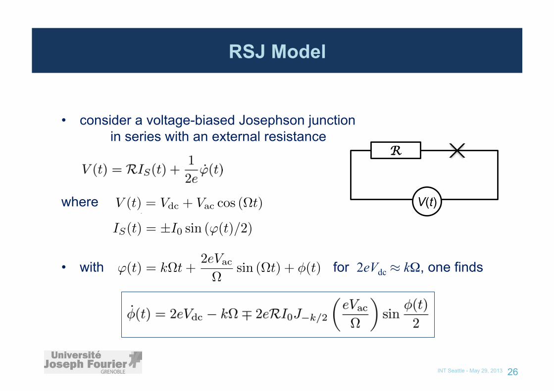
• consider a voltage-biased Josephson junction in series with an external resistance
where • with for 2eVdc ¼ kΩ, one finds
V(t)
R
JSM February 19, 2013 – (S-TI-S : Bound state dynamics – DC & Shapiro.) 2
I. SHAPE OF SHAPIRO STEPS
The voltage-biased RSJ-model is described by the equation
V (t) = RIS(t) +1
2eϕ(t), (10)
where V (t) = Vdc + Vac cos (Ωt) and IS(t) = I0∞
n=0 Bn sin (nϕ(t)/2 + a).We rewrite
ϕ(t) = kΩt+2eVac
Ωsin (Ωt) + φ(t).
Thus,
Vdc + Vac cos (Ωt) = RI0
∞
n=0
Bn sinn2ϕ(t) + a
+
1
2eϕ(t) (11)
⇔ Vdc + Vac cos (Ωt) = RI0
∞
n=1
Bn sin
n
2
kΩt+
2eVac
Ωsin (Ωt) + φ(t)
+ a
+
1
2e
kΩ+ 2eVac cos (Ωt) + φ(t)
(12)
⇔ Vdc −1
2ekΩ = RI0
∞
n=0
Bn
m
J−m
neVac
Ω
sin
nk
2−m
Ωt+
n
2φ(t) + a
+
1
2eφ(t) (13)
RI0
∞
n=0
BnJ−nk/2
neVac
Ω
sin
n2φ(t) + a
+
1
2eφ(t) (14)
for nk/2 ∈ Z and |Vdc − 12ekΩ| Vdc. Keeping only the dominant contribution to a given step, corresponding to the
minimal value m ≡ nmin such that nmink/2 ∈ Z, we obtain
Vdc −1
2ekΩ RI0BmJ−mk/2 (mα) sin
m2φ(t) + a
+
1
2eφ(t), (15)
where α = eVac/Ω.Thus, after rescaling φ → φ = mφ/2,
d
dtφ = meRI0BmJ−mk/2 (nα)
2eVdc − kΩ
2eRI0BmJ−mk/2 (mα)− sin
φ(t) + a
(16)
For |(2eVdc − kΩ)/(2eRI0BmJ−mk/2 (nα))| ≤ 1, we find the constant solution
sin(φ+ a) =2eVdc − kΩ
2eRI0BmJ−mk/2 (mα).
For |(2eVdc − kΩ)/(2eRI0BmJ−mk/2 (mα))| > 1,
dφ
sin(φ+ a) + 2eVdc−kΩCm,k
=m
2Cm,k
dt ⇒ 2π sign
2eVdc − kΩ
Cm,k
1
2eVdc−kΩCm,k
2− 1
=m
2Cm,kT, (17)
where Cm,k = 2eRI0BmJ−mk/2 (mα). Furthermore,
ddt
φ = 2π
T=
m
2Cm,k sign
2eVdc − kΩ
Cm,k
2eVdc − kΩ
Cm,k
2
− 1.
The current is then given as
IS = I0∞
n=1
Bn sinn2ϕ(t) + a
I0BmJ−mk/2 (mα) sin(φ+ a) (18)
= I0BmJ−mk/2 (nα)
2eVdc − kΩ
2eRI0BmJ−mk/2 (nα)− 1
meRI0BmJ−mk/2 (mα) ddt
φ
(19)
=1
2eR
2eVdc − kΩ− Cm,k sign
2eVdc − kΩ
Cm,k
θ
2eVdc − kΩ
Cm,k
2
− 1
2eVdc − kΩ
Cm,k
2
− 1
. (20)
JSM January 18, 2013 – (S-TI-S : Bound state dynamics – Shapiro.) 1
PRELIMINARY NOTES
S-TI-S : Bound state dynamics – Shapiro
January 18, 2013
I. RSJ-MODEL
The voltage-biased RSJ-model is described by the equation
V (t) = RIS(t) +1
2eϕ(t), (1)
where V (t) = Vdc + Vac cos (ωt) and IS(t) = ±I0 sin (ϕ(t)/2).We rescale times t → t = ωt/(2π) and introduce the variable v(t) = ϕ(t) to obtain
ϕ(t) = 2π
2eVdc
ω+
2eVac
ωcos (2πt)∓ 2eI0R
ωsin
ϕ(t)
2
. (2)
Furthermore, we introduce
V =2eVdc
ω, α =
2eVac
ω, IcR =
2eI0R
ω. (3)
Thus,
ϕ(t) = 2π
V + α cos (2πt)− pm IcR sin
ϕ(t)
2
, (4)
where pm takes the values ±1.If pm = −1 (the bound state is filled), at phase ϕ = 4nπ, there is a probablity s of its value to switch to pm = 1. If
pm = 1 (the bound state is empty), at phase ϕ = (4n+2)π, there is a probability s of its value to switch to pm = −1.The coupled equations can be integrated numerically, using an initial phase ϕ0 and including the switching processes
described above. We then compute
I = I01
N + 1
N
n=0
sinϕ(tn)
2. (5)
The noise is calculated as
S(0) =1
N + 1
100
Tmax
Tmax/100−1
n=0
δI ∗(ωn)δI(ωn)
,
where δI is the Fourier transform of δI = I − I.
JSM May 25, 2013 – (S-TI-S : Bound state dynamics – DC & Shapiro.) 2
I. SHAPE OF SHAPIRO STEPS
The voltage-biased RSJ-model is described by the equation
V (t) = RIS(t) +1
2eϕ(t), (10)
where V (t) = Vdc + Vac cos (Ωt) and IS(t) = I0 sin (ϕ(t)/2).We rewrite
ϕ(t) = kΩt+2eVac
Ωsin (Ωt) + φ(t).
Thus,
Vdc + Vac cos (Ωt) = RI0 sin (ϕ(t)/2) +1
2eϕ(t) (11)
⇔ Vdc + Vac cos (Ωt) = RI0 sin
1
2
kΩt+
2eVac
Ωsin (Ωt) + φ(t)
+
1
2e
kΩ+ 2eVac cos (Ωt) + φ(t)
(12)
⇔ Vdc −1
2ekΩ RI0J−k/2
eVac
Ω
sin
φ(t)
2+
1
2eφ(t) (13)
for nk/2 ∈ Z and |Vdc − 12ekΩ| Vdc. Keeping only the dominant contribution to a given step, corresponding to the
minimal value m ≡ nmin such that nmink/2 ∈ Z, we obtain
Vdc −1
2ekΩ RI0BmJ−mk/2 (mα) sin
m2φ(t) + a
+
1
2eφ(t), (14)
where α = eVac/Ω.Thus, after rescaling φ → φ = mφ/2,
d
dtφ = meRI0BmJ−mk/2 (nα)
2eVdc − kΩ
2eRI0BmJ−mk/2 (mα)− sin
φ(t) + a
(15)
For |(2eVdc − kΩ)/(2eRI0BmJ−mk/2 (nα))| ≤ 1, we find the constant solution
sin(φ+ a) =2eVdc − kΩ
2eRI0BmJ−mk/2 (mα).
For |(2eVdc − kΩ)/(2eRI0BmJ−mk/2 (mα))| > 1,
dφ
sin(φ+ a) + 2eVdc−kΩCm,k
=m
2Cm,k
dt ⇒ 2π sign
2eVdc − kΩ
Cm,k
1
2eVdc−kΩCm,k
2− 1
=m
2Cm,kT, (16)
where Cm,k = 2eRI0BmJ−mk/2 (mα). Furthermore,
ddt
φ = 2π
T=
m
2Cm,k sign
2eVdc − kΩ
Cm,k
2eVdc − kΩ
Cm,k
2
− 1.
The current is then given as
IS = I0∞
n=1
Bn sinn2ϕ(t) + a
I0BmJ−mk/2 (mα) sin(φ+ a) (17)
= I0BmJ−mk/2 (nα)
2eVdc − kΩ
2eRI0BmJ−mk/2 (nα)− 1
meRI0BmJ−mk/2 (mα) ddt
φ
(18)
=1
2eR
2eVdc − kΩ− Cm,k sign
2eVdc − kΩ
Cm,k
θ
2eVdc − kΩ
Cm,k
2
− 1
2eVdc − kΩ
Cm,k
2
− 1
. (19)
RSJ Model
INT Seattle - May 29, 2013 27
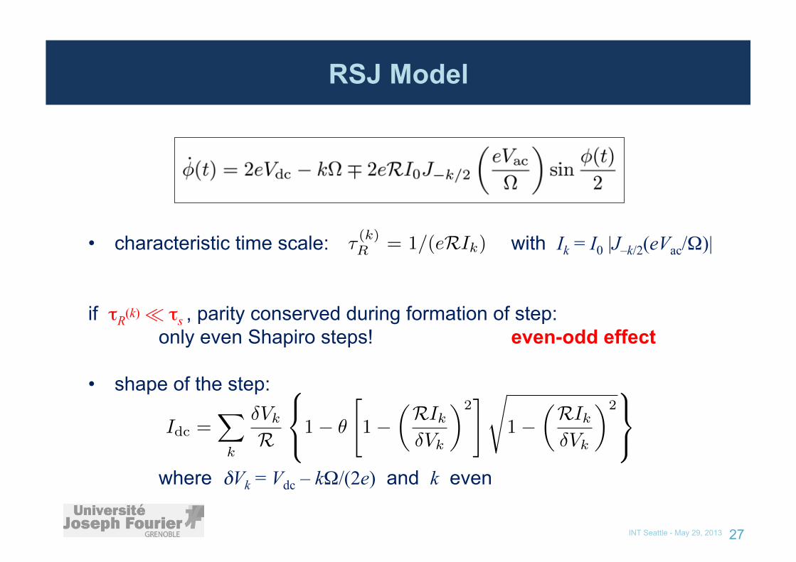
• characteristic time scale: with Ik = I0 |J–k/2(eVac/Ω)| if τR(k) ¿ τs , parity conserved during formation of step:
only even Shapiro steps! even-odd effect • shape of the step:
where δVk = Vdc – kΩ/(2e) and k even
3
!
!
!
!
!
!
!
!
!!!!!!!!!!!!!!!!!!!!!!!!!!!!!!!!!!!!!!!!!!!
s! 1 " 1.05 #2!3
s! 0.93 #"5!4
e"2 #!3
0 1 2 3 4 50.0
0.2
0.4
0.6
0.8
1.0
#$R3!2%!"eVdc#
s
FIG. 1: Switching probability s as a function of the adiabatic-ity parameter λ (dots). The lines correspond to the asymp-totic expressions for s, see text.
through s =
pσ|cpσ(∞)|2, using the initial conditions
cA(−∞) = 1 and cpσ(−∞) = 0. At λ 1, using
cpσ(t) ≈ iϕ(t)ψpσ(t)| ∂H
∂ϕ(t) |ψA(t)pσ − A(t)
e−i t
ds [pσ−A(s)] ,
(7)the amplitudes cpσ(∞) are expressed through integralsthat may be evaluated by a saddle point method. Weobtain s 0.93λ−5/4e−2λ/3. Furthermore, we can iden-tify the time scale over which the transition happens,τt ∼
√R/(eVdc).
At arbitrary λ, the switching probability can beobtained numerically by discretizing Eq. (3) on atight-binding lattice and solving the correspondingSchrodinger equation numerically. The result, togetherwith the asymptotes obtained above, is shown in Fig. 1.
Using the fact that the transition time τt is muchshorter than the Josephson oscillation period, τt π/(eVdc), we may now write an effective discrete Markovmodel for the bound state dynamics, cf. Fig. 2. Usinga discrete time evolution we assume that if the state isfilled, at phase ϕ2n = 4nπ, there is a probability s of theparticle to escape from the bound state to the continuum,whereas if the state is empty, at time ϕ2n+1 = (4n+2)π,there is a probability s of a particle from the continuumfilling the bound state. Thus,
P2n+1
Q2n+1
=
1 s0 1− s
P2n
Q2n
, (8a)
P2n
Q2n
=
1− s 0s 1
P2n−1
Q2n−1
. (8b)
Here Pn is the probability for the state to be occupied,and Qn = 1 − Pn is the probability for the state to beempty at phases ϕn < ϕ(t) < ϕn+1, corresponding ton = Int [ϕ(t)/(2π)]. Solving these equations iteratively,we obtain
P2(n+k) = P∞2n + (1−s)2k (P2n − P∞
2n) , (9a)
P2(n+k)+1 = P∞2n+1 + (1−s)2k+1 (P2n − P∞
2n). (9b)
(a) 5 10 15!!t"#2"0
n!t"
(b)5 10 15
!!t"#2"
#!t"
(c)5 10 15
!!t"#2"
I!t"
FIG. 2: Schematic view of the switching processes due to thecoupling with the continuum: (a) occupation n of the boundstate, (b) energy of the system, and (c) Josephson currentI as a function of time t under dc bias voltage Vdc.
The long-time probabilities at k −1/ ln(1 − s), cor-responding to t τs = −2π/[eVdc ln(1 − s)], are 4π-periodic and independent of the initial state: P∞
n=
[1− (−1)ns/(2− s)]/2.In order to determine the transport properties of the
junction, the switching time τs has to be compared toother characteristic time scales of the system. In par-ticular, if the junction is embedded into a circuit witha resistance R in series, the phase difference across thejunction may adjust over a typical time scale τR ∝ R−1.If τs τR, switching may be neglected (i.e., the
current may be obtained using the initial occupationsP0/Q0). Computing the dc current in the presence of anapplied voltage V (t) = Vdc + Vac cos(Ωt) with Vac Vdc
then yields the even-odd effect discussed in Refs. [8–10].Namely, taking into account a finite resistance R, theaverage current reads
Idc =
k
δVk
R
1− θ
1−
RIkδVk
2
1−RIkδVk
2
,
(10)where Ik = IJ |Jk(α)| is the height of the Shapiro stepat eVdc = kΩ and δVk = Vdc − kΩ/e. Here Jk are theBessel functions and α = eVac/Ω. The characteristic
time scale may be identified as [15, 16] τ (k)R
= 1/(eRIk)at eVdc ∼ kΩ.A small resistance satisfying the relation RIJ Ω is
advantageous for the resolution of Shapiro steps. Fur-thermore, long switching times require s 1. Inthe small-s regime, the time scale τs decreases asexp[2R3/2∆/(3kΩ)] with increasing k. On the otherhand, at small ac perturbation, α 1, the time scale
τ (k)R
increases exponentially with k. The crossover fromτs τR to the opposite limit, τs τR, upon increasingVdc may occur without violation of the condition s 1.This restricts the number of observable Shapiro steps inthe current-voltage characteristics, as we show now. At
3
!
!
!
!
!
!
!
!
!!!!!!!!!!!!!!!!!!!!!!!!!!!!!!!!!!!!!!!!!!!
s! 1 " 1.05 #2!3
s! 0.93 #"5!4
e"2 #!3
0 1 2 3 4 50.0
0.2
0.4
0.6
0.8
1.0
#$R3!2%!"eVdc#
sFIG. 1: Switching probability s as a function of the adiabatic-ity parameter λ (dots). The lines correspond to the asymp-totic expressions for s, see text.
through s =
pσ|cpσ(∞)|2, using the initial conditions
cA(−∞) = 1 and cpσ(−∞) = 0. At λ 1, using
cpσ(t) ≈ iϕ(t)ψpσ(t)| ∂H
∂ϕ(t) |ψA(t)pσ − A(t)
e−i t
ds [pσ−A(s)] ,
(7)the amplitudes cpσ(∞) are expressed through integralsthat may be evaluated by a saddle point method. Weobtain s 0.93λ−5/4e−2λ/3. Furthermore, we can iden-tify the time scale over which the transition happens,τt ∼
√R/(eVdc).
At arbitrary λ, the switching probability can beobtained numerically by discretizing Eq. (3) on atight-binding lattice and solving the correspondingSchrodinger equation numerically. The result, togetherwith the asymptotes obtained above, is shown in Fig. 1.
Using the fact that the transition time τt is muchshorter than the Josephson oscillation period, τt π/(eVdc), we may now write an effective discrete Markovmodel for the bound state dynamics, cf. Fig. 2. Usinga discrete time evolution we assume that if the state isfilled, at phase ϕ2n = 4nπ, there is a probability s of theparticle to escape from the bound state to the continuum,whereas if the state is empty, at time ϕ2n+1 = (4n+2)π,there is a probability s of a particle from the continuumfilling the bound state. Thus,
P2n+1
Q2n+1
=
1 s0 1− s
P2n
Q2n
, (8a)
P2n
Q2n
=
1− s 0s 1
P2n−1
Q2n−1
. (8b)
Here Pn is the probability for the state to be occupied,and Qn = 1 − Pn is the probability for the state to beempty at phases ϕn < ϕ(t) < ϕn+1, corresponding ton = Int [ϕ(t)/(2π)]. Solving these equations iteratively,we obtain
P2(n+k) = P∞2n + (1−s)2k (P2n − P∞
2n) , (9a)
P2(n+k)+1 = P∞2n+1 + (1−s)2k+1 (P2n − P∞
2n). (9b)
(a) 5 10 15!!t"#2"0
n!t"
(b)5 10 15
!!t"#2"
#!t"
(c)5 10 15
!!t"#2"
I!t"
FIG. 2: Schematic view of the switching processes due to thecoupling with the continuum: (a) occupation n of the boundstate, (b) energy of the system, and (c) Josephson currentI as a function of time t under dc bias voltage Vdc.
The long-time probabilities at k −1/ ln(1 − s), cor-responding to t τs = −2π/[eVdc ln(1 − s)], are 4π-periodic and independent of the initial state: P∞
n=
[1− (−1)ns/(2− s)]/2.In order to determine the transport properties of the
junction, the switching time τs has to be compared toother characteristic time scales of the system. In par-ticular, if the junction is embedded into a circuit witha resistance R in series, the phase difference across thejunction may adjust over a typical time scale τR ∝ R−1.If τs τR, switching may be neglected (i.e., the
current may be obtained using the initial occupationsP0/Q0). Computing the dc current in the presence of anapplied voltage V (t) = Vdc + Vac cos(Ωt) with Vac Vdc
then yields the even-odd effect discussed in Refs. [8–10].Namely, taking into account a finite resistance R, theaverage current reads
Idc =
k
δVk
R
1− θ
1−
RIkδVk
2
1−RIkδVk
2
,
(10)where Ik = IJ |Jk(α)| is the height of the Shapiro stepat eVdc = kΩ and δVk = Vdc − kΩ/e. Here Jk are theBessel functions and α = eVac/Ω. The characteristic
time scale may be identified as [15, 16] τ (k)R
= 1/(eRIk)at eVdc ∼ kΩ.A small resistance satisfying the relation RIJ Ω is
advantageous for the resolution of Shapiro steps. Fur-thermore, long switching times require s 1. Inthe small-s regime, the time scale τs decreases asexp[2R3/2∆/(3kΩ)] with increasing k. On the otherhand, at small ac perturbation, α 1, the time scale
τ (k)R
increases exponentially with k. The crossover fromτs τR to the opposite limit, τs τR, upon increasingVdc may occur without violation of the condition s 1.This restricts the number of observable Shapiro steps inthe current-voltage characteristics, as we show now. At

τs ¿ τR : Average Current
INT Seattle - May 29, 2013 28
• non-adiabatic processes important
average current: • determined by long-time probabilities
independent of initial state & 4¼-periodic
• 2¼-periodic • strongly suppressed for s ¿ 1
NOTE: for Vac ¿ Vdc & Ω ¿ δ, dependence of s on ac bias negligible
→ Shapiro steps suppressed
τs ¿ τR : Noise
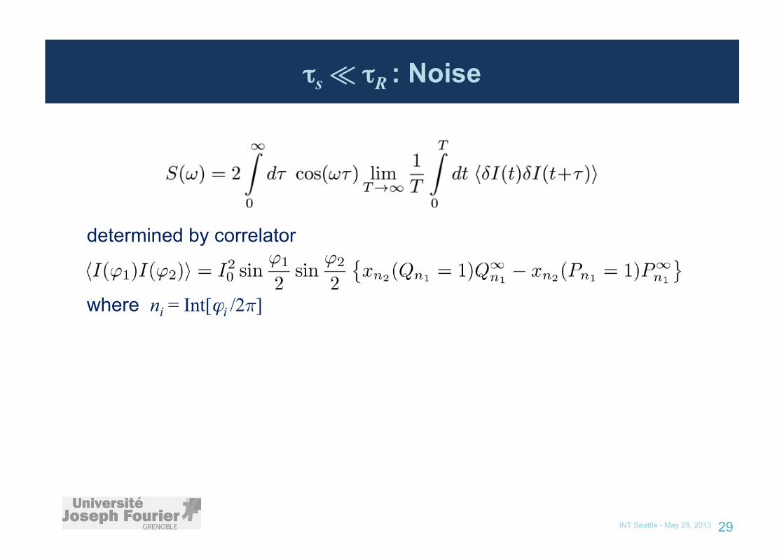
INT Seattle - May 29, 2013 29
determined by correlator where ni = Int[ϕi /2¼]

Noise – DC Bias
INT Seattle - May 29, 2013 30
finite-frequency noise: peak at ! = ± eVdc
for ! ¼ ± eVdc & s ¿ 1
• peak width → characteristic time scale τs
similar results for finite-size Majorana nanowires equivalently: fractional AC effect in transient regime Pikulin & Nazarov 2011 San-José, Prada & Aguado 2012
4
τs τR, we may use the long-time probabilities P∞/Q∞
to compute the current and take the limit τR → ∞. Atlong times, the average current is 2π-periodic,
I(t) = IJ sinϕ(t)
2
Q∞
Int[ϕ(t)/(2π)] − P∞Int[ϕ(t)/(2π)]
=sIJ2− s
sinϕ(t)
2
. (11)
More importantly, Eq. (11) shows that the current is pro-portional to the switching probability s 1. This resultis valid in the presence of microwave irradiation as long asVac Vdc,Ω/e, such that the phase velocity ϕ remainsalways positive [17]. Thus Shapiro steps are strongly sup-pressed, Ik ∝ s.
In order to reveal signatures of the 4π-periodicity inthe regime τs τR, we now turn to the current noisespectrum,
S(ω) = 2
∞
0
dτ cos(ωτ)δI(t)δI(t+ τ), (12)
where δI = I − I and the bar denotes time-averaging.It may be obtained from the correlator I(ϕ1)I(ϕ2) =I2J sin(ϕ1/2) sin(ϕ2/2)[Q∞
n1xn2(Pn1 = 0) − P∞
n1xn2(Pn1 =
1)] at ϕ1 < ϕ2, where ni = Int[ϕi/(2π)]. Using theconditional probabilities obtained from Eqs. (9), we find
δI(ϕ1)δI(ϕ2) =4I2J(1− s)
(2− s)2sin
ϕ1
2sin
ϕ2
2(1− s)n2−n1 .
(13)At dc bias only, the noise spectral density evaluates to
S(ω) =4sI2J
π(2− s)
(eVdc)3
[ω2−(eVdc)2]24 cos2 πω
2eVdc
4 cos2 πω2eVdc
+ s2
1−s
. (14)
If s 1, it has sharp peaks at ω = ±eVdc, i.e., at half ofthe “usual” Josephson frequency:
S(ω) I2J2
seVdc/π
(ω ∓ eVdc)2 + (seVdc/π)2(15)
at |ω ∓ eVdc| eVdc. In particular, the peak widthis 2seVdc/π. The position of the peak reveals the 4π-periodicity of the Andreev bound state whereas the in-verse width characterizes its lifetime τs ∝ s−1. The peakin the noise is due to the transient 4π-periodic behavior[18] of the current at times smaller than the lifetime ofthe bound state.
Under microwave irradiation, the peak may be shiftedto smaller frequencies. In particular, in the limit Vac Vdc,Ω/e, we find
S(ω) I2J2J2k (α)
seVdc/π
[ω ∓ (eVdc−kΩ)]2 + (seVdc/π)2(16)
at |ω∓ (eVdc−kΩ)| eVdc. As above, the peak width isset by the lifetime of the bound state which, thus, may
be probed by noise measurements. Eq. (16) holds forfrequencies ω not too close to zero. In the limit ω →0, additional features related to the Shapiro steps mayappear [16].
While we considered the helical edge states of 2Dtopological insulators, the model is also applicable tonanowires [2, 3] with strong spin-orbit coupling and aZeeman energy much larger than ∆. Note that, in addi-tion to the non-adiabatic processes that we considered,non-adiabatic processes in the vicinity of ϕ = (2n + 1)πbecome important if the zero-energy crossing is splitdue to the presence of additional Majorana modes atthe ends of the wire [18–20]. In particular, in orderto see signatures associated with the 4π-periodicity, theprobability of Landau-Zener tunneling across the gap atϕ = (2n + 1)π would have to be large while the switch-ing probability due to the coupling with the continuum,discussed in this work, remains small.
To summarize, we studied the characteristics of thevoltage-biased topological Josephson junctions. The dy-namic coupling between the Andreev bound state and thecontinuum yields a finite lifetime for the bound state. Ifthat lifetime is longer than the characteristic time scaleover which the phase in the circuit evolves to gener-ate Shapiro steps, these steps display an even-odd ef-fect. However, if the lifetime becomes comparable to thattimescale, signatures in the average current are obscuredwhile the current noise remains sensitive to the under-lying 4π-periodicity of the bound state, which leads tocharacteristic peaks in the noise spectrum. The peaks inthe finite-frequency noise, at dc bias, and low-frequencynoise, with additional ac bias, should be seen easily atvoltages eVdc < R3/2∆, where R is the reflection proba-bility. The peak width is a measure for the rate of parity-changing processes.
In the final stages of preparing the manuscript, we be-came aware of Ref. [21] considering related effects innanowire-based topological Josephson junctions.
We would like to acknowledge helpful discussions withJ. Sau. Part of this research was supported through ANRgrants ANR-11-JS04-003-01 and ANR-12-BS04-0016-03,an EU-FP7 Marie Curie IRG, and DOE under ContractNo. DEFG02-08ER46482. Furthermore, we thank theAspen Center for Physics for hospitality.
[1] L. Fu and C. L. Kane, Phys. Rev. B 79, 161408(R)
(2009).
[2] R. M. Lutchyn, J. D. Sau, and S. Das Sarma, Phys. Rev.
Lett. 105, 077001 (2010).
[3] Y. Oreg, G. Refael, and F. von Oppen, Phys. Rev. Lett.
105, 177002 (2010).
[4] V. Mourik, K. Zuo, S. M. Frolov, S. R. Plissard, E. P. A.
M. Bakkers, and L. P. Kouwenhoven, Science 336, 1003(2012).

Noise – DC+AC Bias
INT Seattle - May 29, 2013 31
noise peak shifted to lower (more accessible?) frequencies under microwave irradiation:
Conclusions I
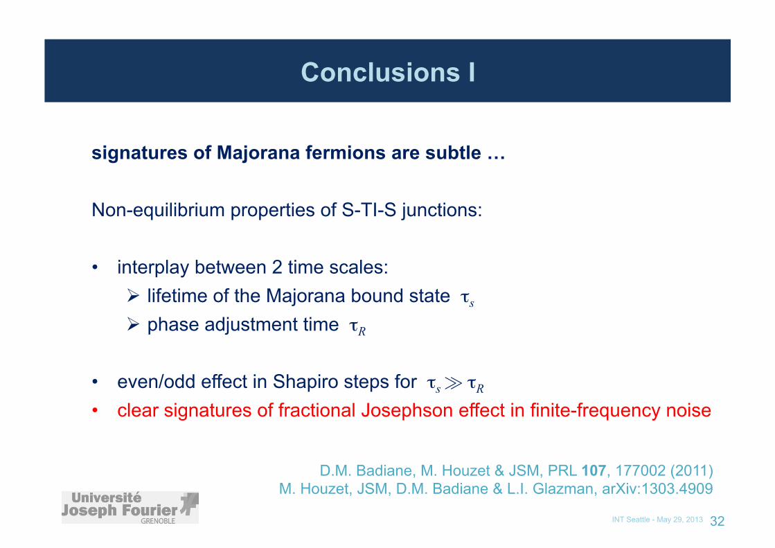
signatures of Majorana fermions are subtle … Non-equilibrium properties of S-TI-S junctions:
• interplay between 2 time scales: Ø lifetime of the Majorana bound state τs
Ø phase adjustment time τR
• even/odd effect in Shapiro steps for τs À τR • clear signatures of fractional Josephson effect in finite-frequency noise
D.M. Badiane, M. Houzet & JSM, PRL 107, 177002 (2011) M. Houzet, JSM, D.M. Badiane & L.I. Glazman, arXiv:1303.4909
INT Seattle - May 29, 2013 32

Alternative Approach: Scattering Theory
INT Seattle - May 29, 2013 33

• electrons/holes gain/lose energy eVdc when traversing the barrier
• only quasi-particles with energy |ε| > Δ can escape into reservoir
I-V characteristics: Multiple Andreev Reflections
INT Seattle - May 29, 2013 34
2eVdc
Superconductor Superconductor
Octavio, Blonder, Tinkham & Klapwijk 1993

Scattering Formalism
INT Seattle - May 29, 2013 35
Superconductor Superconductor

• Andreev reflection:
• scattering matrix for electrons:
+ applied voltage: • scattering matrix for holes:
Scattering Formalism
INT Seattle - May 29, 2013 36
scattering matrix
Andreev reflection
Andreev reflection
Superconductor Superconductor
!1 0 1 "
1!a""#$
e h e h

Scattering Formalism
INT Seattle - May 29, 2013 37
Superconductor Superconductor
• derive recursion relations for coefficients An, Bn
• obtain expression for current:
where
incoming electron from the left
e h e h
D Averin & A Bardas, PRL (1995)

Noise
INT Seattle - May 29, 2013 38
3
be understood due to the energy gap Eg = (1 !"D)!
between the bound states and the continuum. In addi-tion, singularities appear at voltages eV = !/q, where qis an integer [15]. This is to be contrasted with conven-tional Josephson junctions, where singularities appear atvoltages eV = 2!/q. These singularities are associatedwith the energy gap 2! between occupied and emptystates that quasiparticles have to overcome. Namely, newchannels for charge transfer open at the specific voltageseV = 2!/q when quasiparticles can overcome the energygap by performing q ! 1 Andreev reflections. In S/TI/Sjunctions, the presence of the MBS reduces the energygap between occupied and empty states to !.This manifests itself most clearly in the tunneling
regime (D # 1), where one sees a current onset ateV = !, cf. Fig. 1. The analytic expression for thedc current in the tunneling regime reads Itun0 (V ) =(eD/h)
!
d! "(!)"(! ! eV )[f(! ! eV ) ! f(!)]. Here, f(!)is the Fermi distribution, and the normalized density ofstates on either side of the junction, "(!) = #!$(!) +%(|!|!!)
"!2 !!2/|!|, shows the contributions of MBS
and continuum. At T = 0, the current Itun0 is the sumof two terms. The first term corresponds to the transferfrom the continuum to the MBS for voltages eV $ !,whereas the second term corresponds to the (conven-tional) transfer from continuum to continuum for volt-ages eV $ 2!. The suppression of the square-root sin-gularity at the gap edge in "(!) explains that the singularbehavior of I0(V ) at eV = 2! is smooth.For completeness, we provide the analytical expression
for the excess current, Iexc = I0! (e2/h)DV at eV % !,
Iexc = (2e/h)(D2!/R)(1 ! (D/"R) arctan
"R), where
R = 1!D, which varies between 0 in the tunneling limitand (8/3#)Ic at perfect transmission.We now turn to the ac components of the current. Mul-
tiple Andreev reflections yield ac components at multi-ples of the Josephson frequency &J . In particular, con-centrating on the first harmonic I1, we notice that, justas the dc current, both its real and imaginary part showMAR features at eV = !/q. More strikingly, I1 van-ishes in the limit V & 0 (except for perfectly transpar-ent junctions), and in the tunneling limit, I1 is stronglysuppressed even at finite voltages.At first sight, these results seem somewhat paradoxical:
Does the vanishing of I1 indicate the absence of an acJosephson e"ect? In fact, the fractional Josephson e"ectwith frequency &J/2 is absent in the formalism from theoutset, cf. Eq. (6), whereas the regular Josephson e"ectwith frequency &J vanishes at small voltage. The latter isin stark contrast with the case of conventional Josephsonjunctions, where the stationary value of the dc current isrecovered as V & 0 [13].To resolve this puzzle, we study the current-current
correlations. In particular, we consider the (sym-metrized) frequency-dependent current noise,
S(&) =
"
d'ei!" '$I(t)$I(t+') + $I(t+')$I(t)(, (8)
where $I(t) = I(t) ! I(t), and the bar denotes a timeaveraging. In terms of the coe#cients An, Bn, Cn, Dn,the noise can be expressed in the following form,
S(&) =e2
2h
#
±!
#
p
"
d! d!! J(!)J(!!)
$
(f(!)[1! f(!!)] + f(!!)[1 ! f(!)])) (9)
)
%
$(! ! !! ± & + 2peV )&
'
'
'
'
'
#
n
(
A"n+pA
!n + a"2(n+p)a
!2nA
"n+pA
!n ! (1 + a"2(n+p)a
!2n)B
"n+pB
!n
)
'
'
'
'
'
2
+
'
'
'
'
'
#
n
(1 + a"2(n+p)+1a!2n+1)
*
C"n+pC
!n !D"
n+pD!n
+
'
'
'
'
'
2,
+2$(!! !! ± & + (2p! 1)eV )
'
'
'
'
'
#
n
(
A"n+pC
!n + a"2(n+p)a
!2n+1A
"n+pC
!n ! (1 + a"2(n+p)a
!2n+1)B
"n+pD
!n
)
'
'
'
'
'
2 -
+(f(!)f(!!) + [1! f(!)][1! f(!!)]) )
)
%
$(! + !! ± & + 2peV )
'
'
'
'
'
#
n
.
Ap#nB!n !Bp#nA
!n ! a2(p#n)a
!2n
*
Ap#nB!n !Bp#nA
!n
+/
'
'
'
'
'
2
+$(!+ !! ± & + 2(p+ 1)eV )
'
'
'
'
'
#
n
(1! a2(p#n)+1a!2n+1) (Dp#nC
!n ! Cp#nD
!n)
'
'
'
'
'
2
+2$(!+ !! ± & + (2p+ 1)eV )
'
'
'
'
'
#
n
.
Ap#nD!n ! a2(p#n)a
!2n+1Ap#nD
!n !
*
1! a2(p#n)a!2n+1
+
Bp#nC!n
/
'
'
'
'
'
2 -0
.
compute
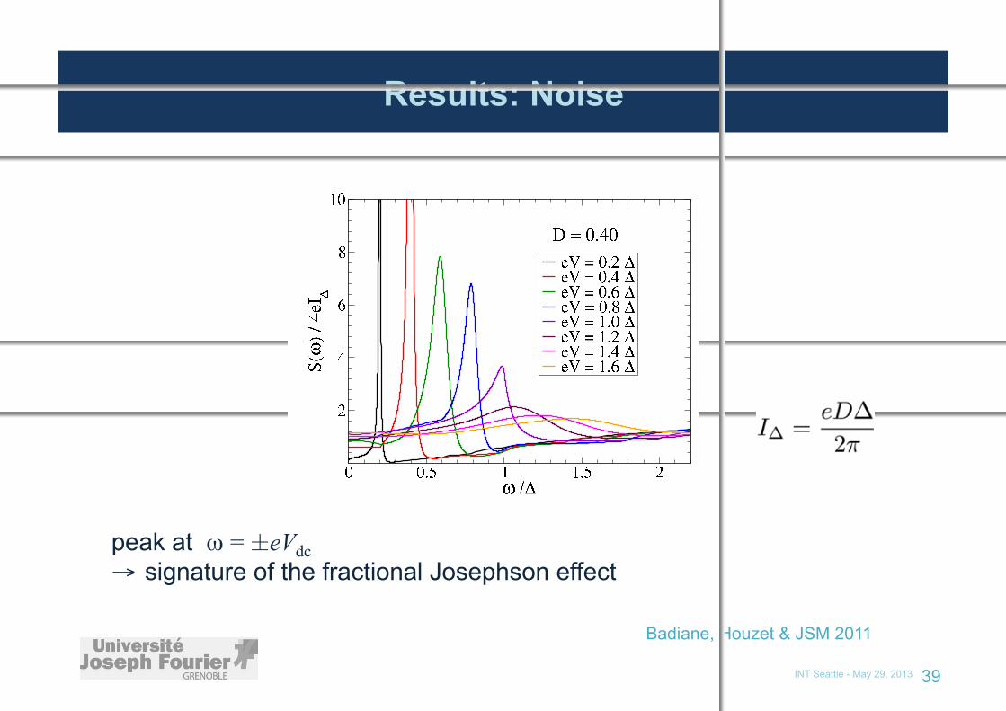
Results: Noise
INT Seattle - May 29, 2013 39
peak at ω = ±eVdc → signature of the fractional Josephson effect Badiane, Houzet & JSM 2011
Non-equilibrium Josephson e!ect through helical edge statesDriss M. Badiane, Manuel Houzet, and Julia S. Meyer
SPSMS, UMR-E CEA / UJF-Grenoble 1, INAC, Grenoble, F-38054, France
A - Motivations
! 2D-topological insulators (TI) admit robust helical edge states withup spins propagating in one direction and down spins in the oppositedirection [1].! Hybrid structures involving superconductors and 2D-TI are expectedto support zero energy Majorana bound states (MBS) [2].! Recent studies predict a fractional Josephson e!ect at half the con-ventional Josephson frequency (!J/2 = eV/!) [3].
In the framework of Landauer-Buttiker formalism we investigate theout-of-equilibrium properties of an S/TI/S junction. We show that:
! MBS signatures are visible in the dc current,
! the fractional Josephson e!ect is not visible in the average current,
! but it can be seen in the finite frequency current noise.
B - The model: equilibrium properties
D: transmission probability
Josephson junction between two s-wavesuperconductors connected through a TI:
H = vp"z#z +M(x)"x +"(x)ei$(x)#z#x
M(x) is a Zeeman field in the junction,"(x) and $(x) are the amplitude and phaseof the superconducting order parameter.
! Andreev bound states:S/TI/S for comparison: S/N/S
0 ! 2 !"1
0
1
#
$!#"#%
0 ! 2 !"1
0
1
#
$!#"#%
%±($) = ±"!D cos ($/2) %±($) = ±"
!
1"D sin2 ($/2)4&-periodic 2&-periodic
Current carried by the Andreev states: I± = 2e'%±(()'( .
$(t) = 2eV t/! =# I $ sin(eV t/!) ?
C - Out of equilibrium properties: current
Applied bias voltage induces multiple Andreev reflections (MAR):wave function for an incoming electron:
#el% (0, t) = J
"
n
#
$
$
%
)n0 + a2nAn
An
Bn
a2nBn
&
'
'
(
e"i(%+n2eV )t/!, 2eV
magnetic barrier characterized by scattering matrices:
Se =
)
r t%
t r%
*
, Sh =
)
"r& t%&
t& "r%&
*
, D = |t|2
Amplitudes in the scattering states can be obtained numerically by a set ofrecursive relations [4].
In terms of these amplitudes the current is given by: I(t) =+
n Inein2eV t,
In =e
h
,
DeV )n0 "-
d% tanh%
2TJ2
.
a&2nA&n + a"2nA"n
+"
m
(1 + a&2(m+n)a2m) (A&m+nAm "B&
m+nBm)
/0
DC current:
! Subgap structures at eV = "/n,(in S/N/S at eV = "/2n)
! tunnel current onset at eV = "(in S/N/S at eV = 2")
Tunnel limit shows a clear signature of MBS:
I tun0 (V ) = (eD/h)
-
d% *(%)*(%" eV )[f (%" eV )" f (%)],
where *(%) is the Normalized DOS on each side of the junction:
*(%) = &")(%) + +(|%|"")!
%2 ""2/|%|.AC current:
I1(V ' 0) ' 0 and I1(D ' 0) ' 0
. Q: Absence of an ac Josephson e!ect?
D - Current noise: probe of 4&-periodicity
Frequency dependent current noise:
S(!) =
-
d#ei!#()I(t), )I(t+# )),
where )I(t) = I(t) " I(t), and the bar de-notes a time averaging.! Peak at ! = eV/! as a consequence ofthe 4&-periodicity.
Broadening of the peak due to dynamical coupling between the bound stateand continuum.
! Tunnel limit: Stun(!) = e+
± I tun0 (V ± !!/e) coth[(eV ± !!)/2T ]
E - Conclusion and perspectives
! Clear signatures of the MBS: MAR features at eV = "/n,
! peak at ! = eV/! in the frequency dependent current noise.(arXiv:1108.3870)
! characteristic time scales for the coupling between the bound state and thecontinuum?
! more realistic models?
References
[1] M. Z. Hasan and C. L. Kane, Rev. Mod. Phys. 82, 3045 (2010).
[2] L. Fu and C. L. Kane, Phys. Rev. B 79, 161408(R) (2009).
[3] H. J. Kwon, K. Sengupta, and V. M. Yakovenko, Eur. Phys. J. B 37, 349(2003).
[4] D. Averin and A. Bardas, Phys. Rev. Lett. 75, 1831 (1995).
email: [email protected]
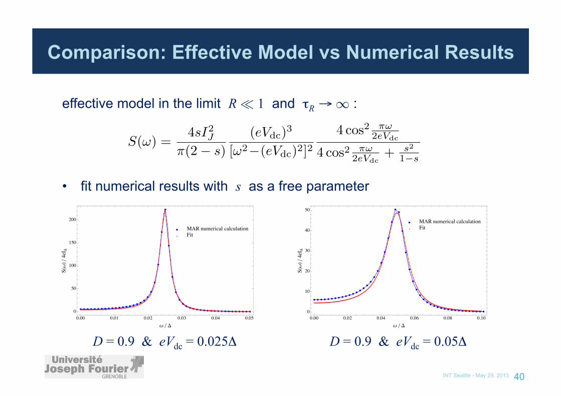
Comparison: Effective Model vs Numerical Results
INT Seattle - May 29, 2013 40
effective model in the limit R ¿ 1 and τR → 1 : • fit numerical results with s as a free parameter
D = 0.9 & eVdc = 0.025Δ D = 0.9 & eVdc = 0.05Δ
4
τs τR, we may use the long-time probabilities P∞/Q∞
to compute the current and take the limit τR → ∞. Atlong times, the average current is 2π-periodic,
I(t) = IJ sinϕ(t)
2
Q∞
Int[ϕ(t)/(2π)] − P∞Int[ϕ(t)/(2π)]
=sIJ2− s
sinϕ(t)
2
. (11)
More importantly, Eq. (11) shows that the current is pro-portional to the switching probability s 1. This resultis valid in the presence of microwave irradiation as long asVac Vdc,Ω/e, such that the phase velocity ϕ remainsalways positive [17]. Thus Shapiro steps are strongly sup-pressed, Ik ∝ s.
In order to reveal signatures of the 4π-periodicity inthe regime τs τR, we now turn to the current noisespectrum,
S(ω) = 2
∞
0
dτ cos(ωτ)δI(t)δI(t+ τ), (12)
where δI = I − I and the bar denotes time-averaging.It may be obtained from the correlator I(ϕ1)I(ϕ2) =I2J sin(ϕ1/2) sin(ϕ2/2)[Q∞
n1xn2(Pn1 = 0) − P∞
n1xn2(Pn1 =
1)] at ϕ1 < ϕ2, where ni = Int[ϕi/(2π)]. Using theconditional probabilities obtained from Eqs. (9), we find
δI(ϕ1)δI(ϕ2) =4I2J(1− s)
(2− s)2sin
ϕ1
2sin
ϕ2
2(1− s)n2−n1 .
(13)At dc bias only, the noise spectral density evaluates to
S(ω) =4sI2J
π(2− s)
(eVdc)3
[ω2−(eVdc)2]24 cos2 πω
2eVdc
4 cos2 πω2eVdc
+ s2
1−s
. (14)
If s 1, it has sharp peaks at ω = ±eVdc, i.e., at half ofthe “usual” Josephson frequency:
S(ω) I2J2
seVdc/π
(ω ∓ eVdc)2 + (seVdc/π)2(15)
at |ω ∓ eVdc| eVdc. In particular, the peak widthis 2seVdc/π. The position of the peak reveals the 4π-periodicity of the Andreev bound state whereas the in-verse width characterizes its lifetime τs ∝ s−1. The peakin the noise is due to the transient 4π-periodic behavior[18] of the current at times smaller than the lifetime ofthe bound state.
Under microwave irradiation, the peak may be shiftedto smaller frequencies. In particular, in the limit Vac Vdc,Ω/e, we find
S(ω) I2J2J2k (α)
seVdc/π
[ω ∓ (eVdc−kΩ)]2 + (seVdc/π)2(16)
at |ω∓ (eVdc−kΩ)| eVdc. As above, the peak width isset by the lifetime of the bound state which, thus, may
be probed by noise measurements. Eq. (16) holds forfrequencies ω not too close to zero. In the limit ω →0, additional features related to the Shapiro steps mayappear [16].
While we considered the helical edge states of 2Dtopological insulators, the model is also applicable tonanowires [2, 3] with strong spin-orbit coupling and aZeeman energy much larger than ∆. Note that, in addi-tion to the non-adiabatic processes that we considered,non-adiabatic processes in the vicinity of ϕ = (2n + 1)πbecome important if the zero-energy crossing is splitdue to the presence of additional Majorana modes atthe ends of the wire [18–20]. In particular, in orderto see signatures associated with the 4π-periodicity, theprobability of Landau-Zener tunneling across the gap atϕ = (2n + 1)π would have to be large while the switch-ing probability due to the coupling with the continuum,discussed in this work, remains small.
To summarize, we studied the characteristics of thevoltage-biased topological Josephson junctions. The dy-namic coupling between the Andreev bound state and thecontinuum yields a finite lifetime for the bound state. Ifthat lifetime is longer than the characteristic time scaleover which the phase in the circuit evolves to gener-ate Shapiro steps, these steps display an even-odd ef-fect. However, if the lifetime becomes comparable to thattimescale, signatures in the average current are obscuredwhile the current noise remains sensitive to the under-lying 4π-periodicity of the bound state, which leads tocharacteristic peaks in the noise spectrum. The peaks inthe finite-frequency noise, at dc bias, and low-frequencynoise, with additional ac bias, should be seen easily atvoltages eVdc < R3/2∆, where R is the reflection proba-bility. The peak width is a measure for the rate of parity-changing processes.
In the final stages of preparing the manuscript, we be-came aware of Ref. [21] considering related effects innanowire-based topological Josephson junctions.
We would like to acknowledge helpful discussions withJ. Sau. Part of this research was supported through ANRgrants ANR-11-JS04-003-01 and ANR-12-BS04-0016-03,an EU-FP7 Marie Curie IRG, and DOE under ContractNo. DEFG02-08ER46482. Furthermore, we thank theAspen Center for Physics for hospitality.
[1] L. Fu and C. L. Kane, Phys. Rev. B 79, 161408(R)
(2009).
[2] R. M. Lutchyn, J. D. Sau, and S. Das Sarma, Phys. Rev.
Lett. 105, 077001 (2010).
[3] Y. Oreg, G. Refael, and F. von Oppen, Phys. Rev. Lett.
105, 177002 (2010).
[4] V. Mourik, K. Zuo, S. M. Frolov, S. R. Plissard, E. P. A.
M. Bakkers, and L. P. Kouwenhoven, Science 336, 1003(2012).
0.00 0.01 0.02 0.03 0.04 0.050
50
100
150
200
Ω
SΩ4eI
MAR numerical calculation Fit
0.00 0.02 0.04 0.06 0.08 0.100
10
20
30
40
50
Ω SΩ
4eI
MAR numerical calculation Fit

!!
!
!
!
!
!
"
"
"
"
"
"
"
!, " D ! 0.85!, " D ! 0.90!, " D ! 0.95
0 1 2 3 4 50.0
0.2
0.4
0.6
0.8
1.0
"!R3!2#!"eVdc#
s
Comparison: Effective Model vs Numerical Results
INT Seattle - May 29, 2013 41
compare with s(λ) (Demkov-Osherov):

INT Seattle - May 29, 2013 42
SNS : I0
0 1 2 3eV/!
0
1
2
3
4
5
6
I 0 / (G
T/e!)
D = 1.00D = 0.99D = 0.90D = 0.70D = 0.50D = 0.30D = 0.10D = 0.01
GT = 2.e2/h.DSTIS : I0
0 1 2 3eV/!
0
1
2
3
4
5
6
I 0 / (G
T/e!)
D = 1.00D = 0.99D = 0.90D = 0.70D = 0.50D = 0.30D = 0.10D = 0.01
GT = 2.e2/h.D
Transparent junction (D = 1): IS-TI-S = 1/2 IS-N-S
Tunnel junction (D → 0): current onset at eVdc = Δ
GN = De2/h GN = 2De2/h
I 0 /
(GN¢
/e)
I 0 /
(GN¢
/e)
For comparison: S-N-S
midgap resonance
eV = 2Δ
Additional Signatures: DC Current

• subgap MAR structures at neVdc = Δ (vs neVdc = 2Δ for S-N-S)
Additional Signatures: DC Current
INT Seattle - May 29, 2013 43
STIS : Log(I0)
0 1 2 3 4 5 6!/eV
-10
-5
0
Log(
I/(G
/e!
) )
D = 0.90D = 0.70D = 0.50D = 0.30D = 0.10D = 0.01
G = e2/h
n = 2 n = 3
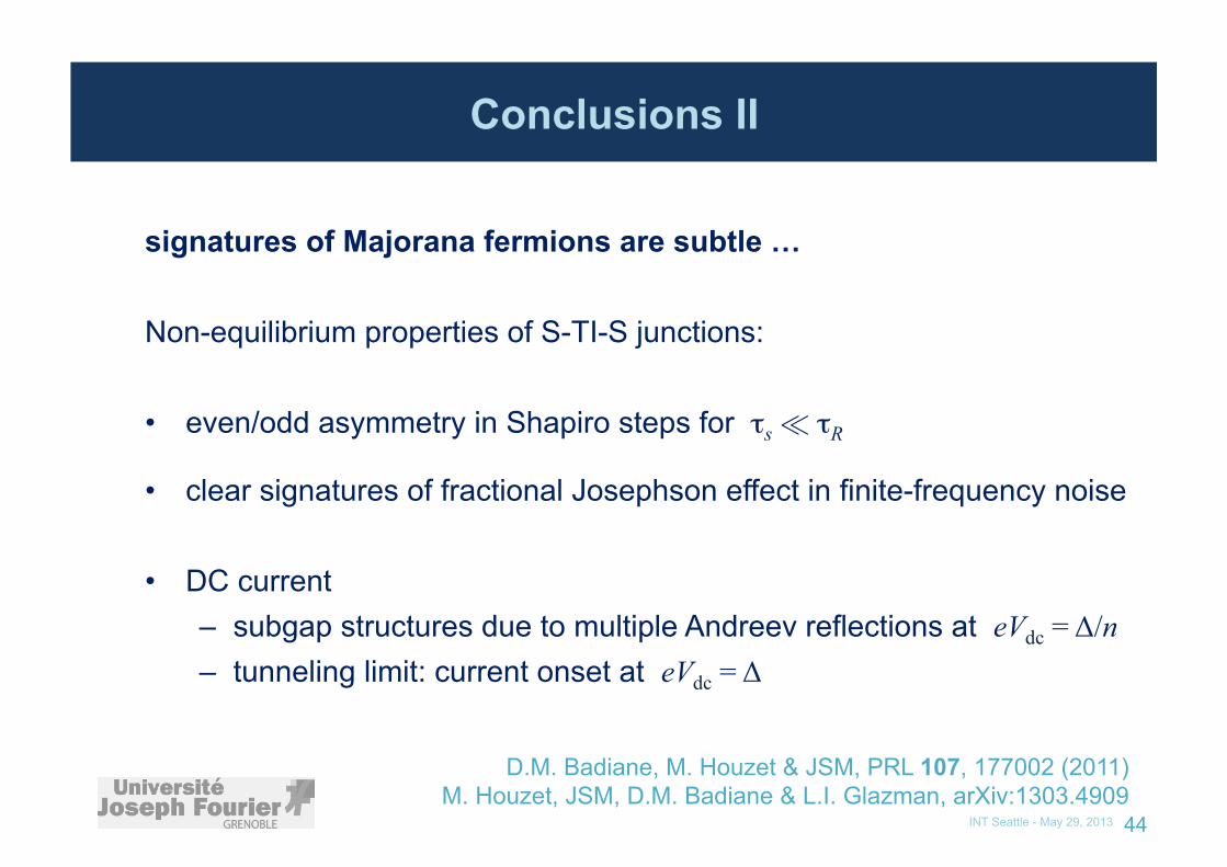
Conclusions II
signatures of Majorana fermions are subtle … Non-equilibrium properties of S-TI-S junctions:
• even/odd asymmetry in Shapiro steps for τs ¿ τR
• clear signatures of fractional Josephson effect in finite-frequency noise
• DC current – subgap structures due to multiple Andreev reflections at eVdc = Δ/n – tunneling limit: current onset at eVdc = Δ
D.M. Badiane, M. Houzet & JSM, PRL 107, 177002 (2011) M. Houzet, JSM, D.M. Badiane & L.I. Glazman, arXiv:1303.4909
INT Seattle - May 29, 2013 44

Thank you!
INT Seattle - May 29, 2013 45


![arXiv:1805.10435v1 [cond-mat.supr-con] 26 May 2018 · Unusual Superconducting Proximity E ect in Magnetically Doped Topological Josephson Junctions Rikizo Yano,1, Masao Koyanagi,](https://static.cupdf.com/doc/110x72/5fb40744e9e5871fb130a368/arxiv180510435v1-cond-matsupr-con-26-may-2018-unusual-superconducting-proximity.jpg)


![Quantum Bits with Josephson Junctions · etc. [2]. This great reliance on Josephson junctions sets constraints on the operating temperature and frequency of the superconducting circuits](https://static.cupdf.com/doc/110x72/5ec5592a13b08355f20aa431/quantum-bits-with-josephson-junctions-etc-2-this-great-reliance-on-josephson.jpg)