V o l t a g e P r o t e c t i o n D e v i c e s
February 2020
V o l t a g e P r o t e c t i o n D e v i c e s
February 2020
AVRM/AVR-M : Standard Type
AVRL : Low Capacitance Type
AVRH : High reliability Type
SGNE : Low Clamp Type
Chip varistors ESD/Voltage protection devices
AVR/SGNE series
REACHSVHC-Free
LeadFreeRoHS
Pb
HalogenFree
BrCl

(2/12)
20200217 / vpd_varistors_avr_en.fm
V o l t a g e P r o t e c t i o n D e v i c e s
Chip varistors
CHARACTERISTICS OF CHIP VARISTOR
Varistors are voltage dependent nonlinear resistive elements witha resistance that decreases rapidly when the voltage is over theconstant value.Varistors become zener diode of 2 serial connection and equiva-lent, and does not have polarity.
CURRENT vs. VOLTAGE CHARACTERISTICS
THE EFFECT OF THE VARISTORWithout varistorA malfunction and failure of electronic equipment
With VaristorSuppress abnormal voltage by inserting varistor in a circuit
EQUIVALENT CIRCUIT OF CHIP VARISTORS
CHIP VARISTORS FEATUREIEC61000-4-2 LEVEL4 compliant.Reliability characteristics evaluated based on AEC-Q200 con-dition. (Automotive products)High ESD withstanding voltageSmall-sized products are available125°C, 150°C Supported
Fig.1 Internal structure of multilayer chip varistors
Overview of the AVR/SGNE series
RoHS Directive Compliant ProductCompatible with lead-free solders
Chip varistor/V1mA:12V
Zener diode/Vz:6.8V
Positive direction
Negative direction
Voltage(V)
Cur
rent
( A) 10–1
10–2
10–3
10–4
10–5
–10–1
–10–2
–10–3
–10–4
–10–52–2 6–6 10–10 14–14 18–18
ESD, Surge voltage
Power lineSignal line
IC
ESD, Surge voltage
Power lineSignal line
Insert a varistor betweena line and ground
: Chip varistor
IC
No. Name(1) Semiconductor ceramics(2) Internal electrode(Pd)(3)
Terminal electrodeAg
(4) Ni(5) Sn
2 Zener Diodes
A capacitance content
②
③④⑤
①
(3/12)
20200217 / vpd_varistors_avr_en.fm
Please be sure to request delivery specifications that provide further details on the features and specifications of the products for proper and safe use.Please note that the contents may change without any prior notice due to reasons such as upgrading.
V o l t a g e P r o t e c t i o n D e v i c e s
Chip varistors
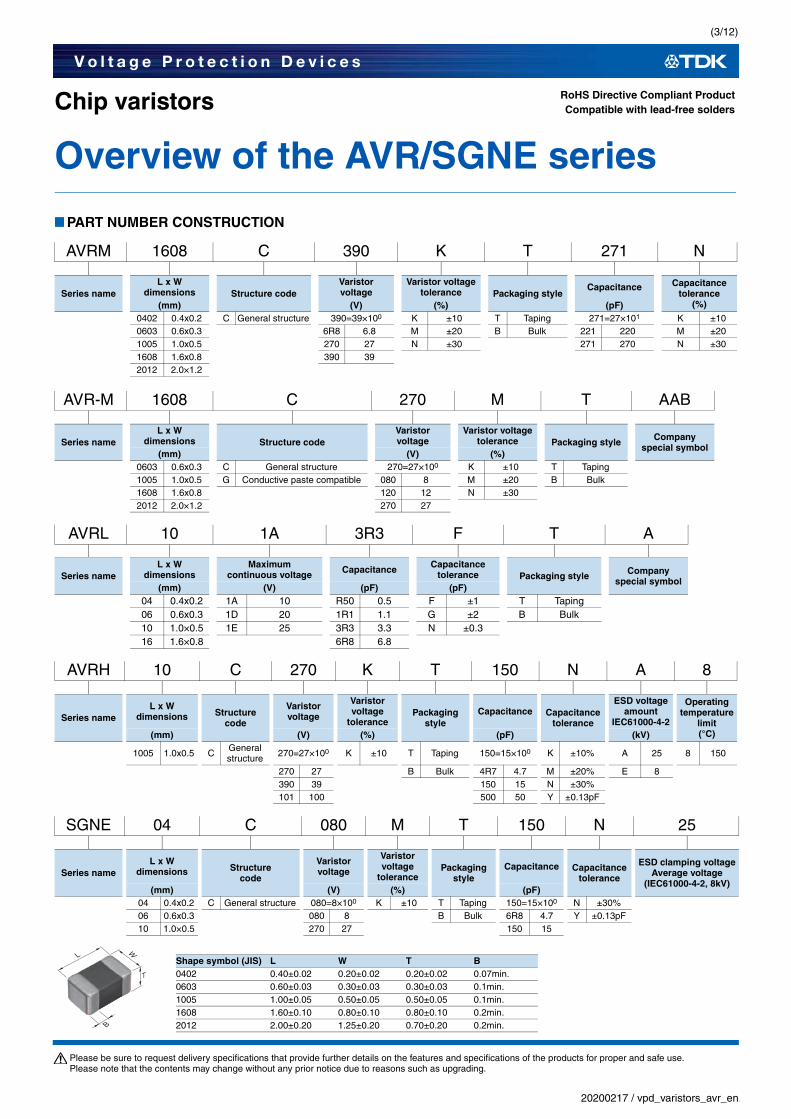
PART NUMBER CONSTRUCTION
Overview of the AVR/SGNE series
AVRM 1608 C 390 K T 271 N
Series nameL x W
dimensions Structure codeVaristor voltage
Varistor voltage tolerance Packaging style
Capacitance Capacitance tolerance
(%)(mm) (V) (%) (pF)0402 0.4x0.2 C General structure 390=39×100 K ±10 T Taping 271=27×101 K ±100603 0.6x0.3 6R8 6.8 M ±20 B Bulk 221 220 M ±201005 1.0x0.5 270 27 N ±30 271 270 N ±301608 1.6x0.8 390 392012 2.0×1.2
AVR-M 1608 C 270 M T AAB
Series nameL x W
dimensions Structure codeVaristor voltage
Varistor voltage tolerance Packaging style Company
special symbol(mm) (V) (%)
0603 0.6x0.3 C General structure 270=27×100 K ±10 T Taping1005 1.0x0.5 G Conductive paste compatible 080 8 M ±20 B Bulk1608 1.6x0.8 120 12 N ±302012 2.0×1.2 270 27
AVRL 10 1A 3R3 F T A
Series nameL x W
dimensionsMaximum
continuous voltage Capacitance Capacitance tolerance Packaging style Company
special symbol(mm) (V) (pF) (pF)
04 0.4x0.2 1A 10 R50 0.5 F ±1 T Taping06 0.6x0.3 1D 20 1R1 1.1 G ±2 B Bulk10 1.0×0.5 1E 25 3R3 3.3 N ±0.316 1.6×0.8 6R8 6.8
AVRH 10 C 270 K T 150 N A 8
Series nameL x W
dimensions Structure code
Varistor voltage
Varistor voltage
tolerancePackaging
styleCapacitance Capacitance
tolerance
ESD voltage amount
IEC61000-4-2
Operating temperature
limit(°C)(mm) (V) (%) (pF) (kV)
1005 1.0x0.5 C General structure 270=27×100 K ±10 T Taping 150=15×100 K ±10% A 25 8 150
270 27 B Bulk 4R7 4.7 M ±20% E 8390 39 150 15 N ±30%101 100 500 50 Y ±0.13pF
SGNE 04 C 080 M T 150 N 25
Series nameL x W
dimensions Structure code
Varistor voltage
Varistor voltage
tolerancePackaging
styleCapacitance Capacitance
tolerance
ESD clamping voltageAverage voltage
(IEC61000-4-2, 8kV)(mm) (V) (%) (pF)
04 0.4x0.2 C General structure 080=8×100 K ±10 T Taping 150=15×100 N ±30%06 0.6x0.3 080 8 B Bulk 6R8 4.7 Y ±0.13pF10 1.0×0.5 270 27 150 15
Shape symbol (JIS) L W T B0402 0.40±0.02 0.20±0.02 0.20±0.02 0.07min.0603 0.60±0.03 0.30±0.03 0.30±0.03 0.1min.1005 1.00±0.05 0.50±0.05 0.50±0.05 0.1min.1608 1.60±0.10 0.80±0.10 0.80±0.10 0.2min.2012 2.00±0.20 1.25±0.20 0.70±0.20 0.2min.
RoHS Directive Compliant ProductCompatible with lead-free solders
W
T
L
B

(4/12)
20200217 / vpd_varistors_avr_en.fm
Please be sure to request delivery specifications that provide further details on the features and specifications of the products for proper and safe use.Please note that the contents may change without any prior notice due to reasons such as upgrading.
V o l t a g e P r o t e c t i o n D e v i c e s
Chip varistors
TERMINOLOGY
1 8/20µs test waveform 2 10/1000µs test waveform
Overview of the AVR/SGNE series
Item Unit DescriptionVaristor voltage(Breakdown voltage)
V1mA
(V)Chip varistor-terminal voltage when DC1mA was flowed
Maximum continuous voltageVdc(V)
DC voltage that is continuously applied between chip varistor terminalsTerminal chip varistors leakage current-value: 50µA max.Voltage appearing across the varistor when a pulse current (8/20µs?1) of specified peak value isapplied.
Clamping voltageVcl(V)
Voltage between terminal chip varistors of the Specified peak current value of the impulse current (8/20µs1) is applied
Maximum energyE(Joule)
When applied specified peak impulse current-value current (10/1000µs2) once, maximum energy thatelectrical property of chip varistors be not deteriorated
Maximum peak currentIp(A)
When applied impulse current (8/20µs1) once, maximum current that electrical property of chip varis-tors be not deteriorated
CapacitanceC(pF)
Oscillator frequency 1kHz or 1MHz, capacitance between chip varistor-terminal in oscillator voltage 1Vrms
RoHS Directive Compliant ProductCompatible with lead-free solders
20µs
50%
90%100%
Cur
rent
Time
8µs1000µs
50%
90%100%
10µs
Cur
rent
Time
(5/12)
20200217 / vpd_varistors_avr_en.fm
Please be sure to request delivery specifications that provide further details on the features and specifications of the products for proper and safe use.Please note that the contents may change without any prior notice due to reasons such as upgrading.
V o l t a g e P r o t e c t i o n D e v i c e s
Chip varistors
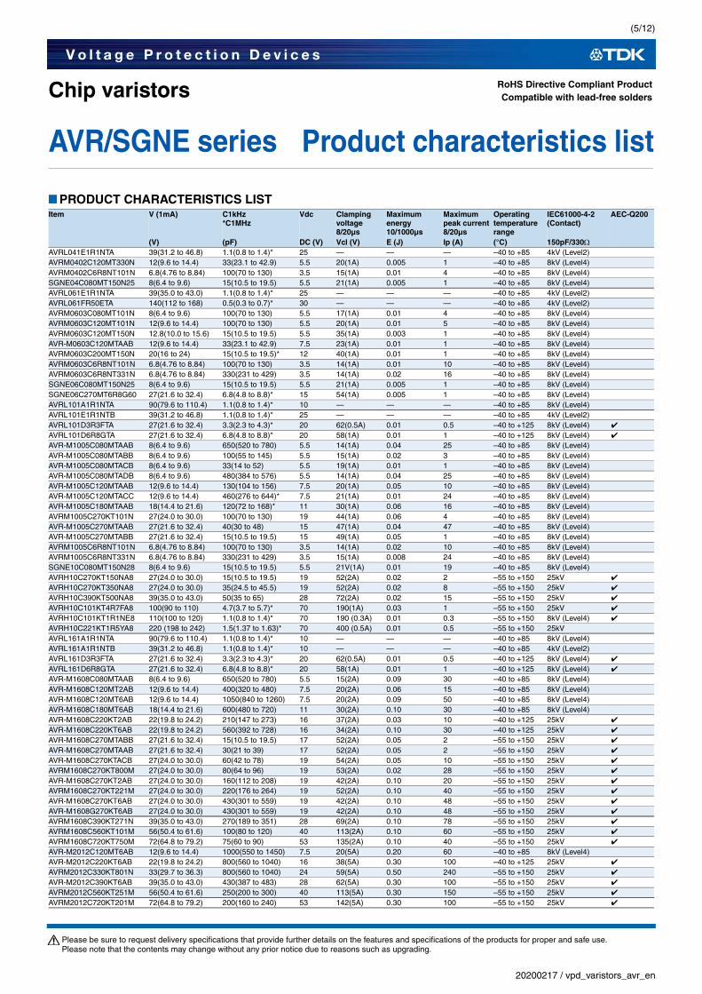
PRODUCT CHARACTERISTICS LIST
AVR/SGNE series Product characteristics list
Item V (1mA) C1kHz*C1MHz
Vdc Clamping voltage8/20µs
Maximum energy10/1000µs
Maximum peak current8/20µs
Operating temperature range
IEC61000-4-2(Contact)
AEC-Q200
(V) (pF) DC (V) Vcl (V) E (J) Ip (A) (°C) 150pF/330AVRL041E1R1NTA 39(31.2 to 46.8) 1.1(0.8 to 1.4)* 25 — — — –40 to +85 4kV (Level2)AVRM0402C120MT330N 12(9.6 to 14.4) 33(23.1 to 42.9) 5.5 20(1A) 0.005 1 –40 to +85 8kV (Level4)AVRM0402C6R8NT101N 6.8(4.76 to 8.84) 100(70 to 130) 3.5 15(1A) 0.01 4 –40 to +85 8kV (Level4)SGNE04C080MT150N25 8(6.4 to 9.6) 15(10.5 to 19.5) 5.5 21(1A) 0.005 1 –40 to +85 8kV (Level4)AVRL061E1R1NTA 39(35.0 to 43.0) 1.1(0.8 to 1.4)* 25 — — — –40 to +85 4kV (Level2)AVRL061FR50ETA 140(112 to 168) 0.5(0.3 to 0.7)* 30 — — — –40 to +85 4kV (Level2)AVRM0603C080MT101N 8(6.4 to 9.6) 100(70 to 130) 5.5 17(1A) 0.01 4 –40 to +85 8kV (Level4)AVRM0603C120MT101N 12(9.6 to 14.4) 100(70 to 130) 5.5 20(1A) 0.01 5 –40 to +85 8kV (Level4)AVRM0603C120MT150N 12.8(10.0 to 15.6) 15(10.5 to 19.5) 5.5 35(1A) 0.003 1 –40 to +85 8kV (Level4)AVR-M0603C120MTAAB 12(9.6 to 14.4) 33(23.1 to 42.9) 7.5 23(1A) 0.01 1 –40 to +85 8kV (Level4)AVRM0603C200MT150N 20(16 to 24) 15(10.5 to 19.5)* 12 40(1A) 0.01 1 –40 to +85 8kV (Level4)AVRM0603C6R8NT101N 6.8(4.76 to 8.84) 100(70 to 130) 3.5 14(1A) 0.01 10 –40 to +85 8kV (Level4)AVRM0603C6R8NT331N 6.8(4.76 to 8.84) 330(231 to 429) 3.5 14(1A) 0.02 16 –40 to +85 8kV (Level4)SGNE06C080MT150N25 8(6.4 to 9.6) 15(10.5 to 19.5) 5.5 21(1A) 0.005 1 –40 to +85 8kV (Level4)SGNE06C270MT6R8G60 27(21.6 to 32.4) 6.8(4.8 to 8.8)* 15 54(1A) 0.005 1 –40 to +85 8kV (Level4)AVRL101A1R1NTA 90(79.6 to 110.4) 1.1(0.8 to 1.4)* 10 — — — –40 to +85 8kV (Level4)AVRL101E1R1NTB 39(31.2 to 46.8) 1.1(0.8 to 1.4)* 25 — — — –40 to +85 4kV (Level2)AVRL101D3R3FTA 27(21.6 to 32.4) 3.3(2.3 to 4.3)* 20 62(0.5A) 0.01 0.5 –40 to +125 8kV (Level4) ✔
AVRL101D6R8GTA 27(21.6 to 32.4) 6.8(4.8 to 8.8)* 20 58(1A) 0.01 1 –40 to +125 8kV (Level4) ✔
AVR-M1005C080MTAAB 8(6.4 to 9.6) 650(520 to 780) 5.5 14(1A) 0.04 25 –40 to +85 8kV (Level4)AVR-M1005C080MTABB 8(6.4 to 9.6) 100(55 to 145) 5.5 15(1A) 0.02 3 –40 to +85 8kV (Level4)AVR-M1005C080MTACB 8(6.4 to 9.6) 33(14 to 52) 5.5 19(1A) 0.01 1 –40 to +85 8kV (Level4)AVR-M1005C080MTADB 8(6.4 to 9.6) 480(384 to 576) 5.5 14(1A) 0.04 25 –40 to +85 8kV (Level4)AVR-M1005C120MTAAB 12(9.6 to 14.4) 130(104 to 156) 7.5 20(1A) 0.05 10 –40 to +85 8kV (Level4)AVR-M1005C120MTACC 12(9.6 to 14.4) 460(276 to 644)* 7.5 21(1A) 0.01 24 –40 to +85 8kV (Level4)AVR-M1005C180MTAAB 18(14.4 to 21.6) 120(72 to 168)* 11 30(1A) 0.06 16 –40 to +85 8kV (Level4)AVRM1005C270KT101N 27(24.0 to 30.0) 100(70 to 130) 19 44(1A) 0.06 4 –40 to +85 8kV (Level4)AVR-M1005C270MTAAB 27(21.6 to 32.4) 40(30 to 48) 15 47(1A) 0.04 47 –40 to +85 8kV (Level4)AVR-M1005C270MTABB 27(21.6 to 32.4) 15(10.5 to 19.5) 15 49(1A) 0.05 1 –40 to +85 8kV (Level4)AVRM1005C6R8NT101N 6.8(4.76 to 8.84) 100(70 to 130) 3.5 14(1A) 0.02 10 –40 to +85 8kV (Level4)AVRM1005C6R8NT331N 6.8(4.76 to 8.84) 330(231 to 429) 3.5 15(1A) 0.008 24 –40 to +85 8kV (Level4)SGNE10C080MT150N28 8(6.4 to 9.6) 15(10.5 to 19.5) 5.5 21V(1A) 0.01 19 –40 to +85 8kV (Level4)AVRH10C270KT150NA8 27(24.0 to 30.0) 15(10.5 to 19.5) 19 52(2A) 0.02 2 –55 to +150 25kV ✔
AVRH10C270KT350NA8 27(24.0 to 30.0) 35(24.5 to 45.5) 19 52(2A) 0.02 8 –55 to +150 25kV ✔
AVRH10C390KT500NA8 39(35.0 to 43.0) 50(35 to 65) 28 72(2A) 0.02 15 –55 to +150 25kV ✔
AVRH10C101KT4R7FA8 100(90 to 110) 4.7(3.7 to 5.7)* 70 190(1A) 0.03 1 –55 to +150 25kV ✔
AVRH10C101KT1R1NE8 110(100 to 120) 1.1(0.8 to 1.4)* 70 190 (0.3A) 0.01 0.3 –55 to +150 8kV (Level4) ✔
AVRH10C221KT1R5YA8 220 (198 to 242) 1.5(1.37 to 1.63)* 70 400 (0.5A) 0.01 0.5 –55 to +150 25kVAVRL161A1R1NTA 90(79.6 to 110.4) 1.1(0.8 to 1.4)* 10 — — — –40 to +85 8kV (Level4)AVRL161A1R1NTB 39(31.2 to 46.8) 1.1(0.8 to 1.4)* 10 — — — –40 to +85 4kV (Level2)AVRL161D3R3FTA 27(21.6 to 32.4) 3.3(2.3 to 4.3)* 20 62(0.5A) 0.01 0.5 –40 to +125 8kV (Level4) ✔
AVRL161D6R8GTA 27(21.6 to 32.4) 6.8(4.8 to 8.8)* 20 58(1A) 0.01 1 –40 to +125 8kV (Level4) ✔
AVR-M1608C080MTAAB 8(6.4 to 9.6) 650(520 to 780) 5.5 15(2A) 0.09 30 –40 to +85 8kV (Level4)AVR-M1608C120MT2AB 12(9.6 to 14.4) 400(320 to 480) 7.5 20(2A) 0.06 15 –40 to +85 8kV (Level4)AVR-M1608C120MT6AB 12(9.6 to 14.4) 1050(840 to 1260) 7.5 20(2A) 0.09 50 –40 to +85 8kV (Level4)AVR-M1608C180MT6AB 18(14.4 to 21.6) 600(480 to 720) 11 30(2A) 0.10 30 –40 to +85 8kV (Level4)AVR-M1608C220KT2AB 22(19.8 to 24.2) 210(147 to 273) 16 37(2A) 0.03 10 –40 to +125 25kV ✔
AVR-M1608C220KT6AB 22(19.8 to 24.2) 560(392 to 728) 16 34(2A) 0.10 30 –40 to +125 25kV ✔
AVR-M1608C270MTABB 27(21.6 to 32.4) 15(10.5 to 19.5) 17 52(2A) 0.05 2 –55 to +150 25kV ✔
AVR-M1608C270MTAAB 27(21.6 to 32.4) 30(21 to 39) 17 52(2A) 0.05 2 –55 to +150 25kV ✔
AVR-M1608C270KTACB 27(24.0 to 30.0) 60(42 to 78) 19 54(2A) 0.05 10 –55 to +150 25kV ✔
AVRM1608C270KT800M 27(24.0 to 30.0) 80(64 to 96) 19 53(2A) 0.02 28 –55 to +150 25kV ✔
AVR-M1608C270KT2AB 27(24.0 to 30.0) 160(112 to 208) 19 42(2A) 0.10 20 –55 to +150 25kV ✔
AVRM1608C270KT221M 27(24.0 to 30.0) 220(176 to 264) 19 52(2A) 0.10 40 –55 to +150 25kV ✔
AVR-M1608C270KT6AB 27(24.0 to 30.0) 430(301 to 559) 19 42(2A) 0.10 48 –55 to +150 25kV ✔
AVR-M1608G270KT6AB 27(24.0 to 30.0) 430(301 to 559) 19 42(2A) 0.10 48 –55 to +150 25kV ✔
AVRM1608C390KT271N 39(35.0 to 43.0) 270(189 to 351) 28 69(2A) 0.10 78 –55 to +150 25kV ✔
AVRM1608C560KT101M 56(50.4 to 61.6) 100(80 to 120) 40 113(2A) 0.10 60 –55 to +150 25kV ✔
AVRM1608C720KT750M 72(64.8 to 79.2) 75(60 to 90) 53 135(2A) 0.10 40 –55 to +150 25kV ✔
AVR-M2012C120MT6AB 12(9.6 to 14.4) 1000(550 to 1450) 7.5 20(5A) 0.20 60 –40 to +85 8kV (Level4)AVR-M2012C220KT6AB 22(19.8 to 24.2) 800(560 to 1040) 16 38(5A) 0.30 100 –40 to +125 25kV ✔
AVRM2012C330KT801N 33(29.7 to 36.3) 800(560 to 1040) 24 59(5A) 0.50 240 –55 to +150 25kV ✔
AVR-M2012C390KT6AB 39(35.0 to 43.0) 430(387 to 483) 28 62(5A) 0.30 100 –55 to +150 25kV ✔
AVRM2012C560KT251M 56(50.4 to 61.6) 250(200 to 300) 40 113(5A) 0.30 150 –55 to +150 25kV ✔
AVRM2012C720KT201M 72(64.8 to 79.2) 200(160 to 240) 53 142(5A) 0.30 100 –55 to +150 25kV ✔
RoHS Directive Compliant ProductCompatible with lead-free solders

(6/12)
20200217 / vpd_varistors_avr_en.fm
Please be sure to request delivery specifications that provide further details on the features and specifications of the products for proper and safe use.Please note that the contents may change without any prior notice due to reasons such as upgrading.
V o l t a g e P r o t e c t i o n D e v i c e s
Chip varistors
DISCHARGE VOLTAGE WAVEFORM (EXAMPLE)
WITHOUT VARISTOR, WAVEFORM AT VARISTOR INSTALLATION WAVEFORM AT VARISTOR INSTALLATION
Test conditions
150pF/330 (IEC61000-4-2)
Contact discharge, Charged voltage 8kV
TEST CIRCUIT DIAGRAM
AVR/SGNE series Electrostatic absorption characteristics
RoHS Directive Compliant ProductCompatible with lead-free solders
–50 0 50 100 150 200 250 300Time(ns)
Vol
tage
( V)
1600
12001000
800
400600
200
–200
1800
1400
0
Without Varistor
AVRH10C270KT150NA8
AVR-M1608C270KT6AB
AVR-M1608C220KT6AB
–50 0 50 100 150 200 250 300Time(ns)
Vol
tage
( V)
160
120100
80
4060
20
–20
180
140
0
AVRH10C270KT150NA8
AVR-M1608C270KT6AB
AVR-M1608C220KT6AB
50Ω
Discharge gun
ESDsimulator
Testsample
Oscilloscope
60dB attenuator
I/O impedance: 50Ω
ESD Simulator
DischargePoint
ChipVaristor
PCB
SMAConnector
CoaxialCable
Attenuator(60dB)50Ω
Oscilloscope50Ω
Shield

(7/12)
20200217 / vpd_varistors_avr_en.fm
Please be sure to request delivery specifications that provide further details on the features and specifications of the products for proper and safe use.Please note that the contents may change without any prior notice due to reasons such as upgrading.
V o l t a g e P r o t e c t i o n D e v i c e s
Chip varistors
Board design
When attached to chip varistors, amount of silver used (fillet size)
has direct impact on chip varistors after mounting. Thus, sufficient
consideration is necessary.
Set of land dimensions(1) As the stress rises in the chip varistors owing to the increase in
silver, breakage and cracks will occur. Cause including crack, as
caution on board land design, configure the shape and dimensions
so that the amount of silver is appropriate. If you installed 2 or
more parts in the Common Land, separated by a solder resist and
special land of each component.
(2) When peak levels panning-at soldering is excessive, by solder
contraction stress, mechanical-thermal stress causes a Yasuku
chip crack. In addition, when the peak level is underestimated, ter-
minal electrode fixed strength is insufficient. This causes chip
dropouts and may affect circuit reliability. Representative example
of the panning of peak levels is shown in the following.
Recommended silver dose
Case and suggested protocol want to avoid
Attention on a circuit board design
RoHS Directive Compliant ProductCompatible with lead-free solders
Dimensions shapeSymbolA B C
0402 0.20 Nom. 0.15 to 0.21 0.18 to 0.200603 0.25 to 0.35 0.20 to 0.30 0.25 to 0.351005 0.30 to 0.50 0.35 to 0.45 0.40 to 0.601608 0.60 to 0.80 0.60 to 0.80 0.60 to 0.802012 0.90 to 1.20 0.70 to 0.90 0.90 to 1.20
AB
C
Solder volume overload
Solder stress is increased, and it is easy for a crack to form.
Decent solder volume
Solder volume deficit
Fixed strength is weak, and there is connection a prob-lem and risk of loss.
Example Cases to avoidImprovement example (land division)
Lead wire and land of part discrete doubles up
Arrangements in the vicinity
Arrangements of chip component's companion
Most large serving amountMinimum prime amount
SolderChip
Leads
PCB
Solder resist
Leads
Solder(ground solder)
Chassis
L1
Solder resist
L2 L2>L1
Land
Land
Excess solder
Missing solder
Solder resist
(8/12)
20200217 / vpd_varistors_avr_en.fm
Please be sure to request delivery specifications that provide further details on the features and specifications of the products for proper and safe use.Please note that the contents may change without any prior notice due to reasons such as upgrading.
V o l t a g e P r o t e c t i o n D e v i c e s
Chip varistors
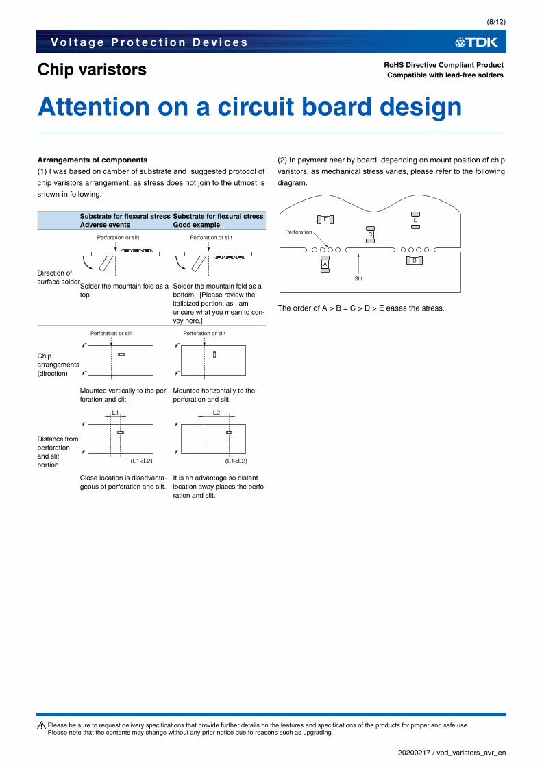
Arrangements of components(1) I was based on camber of substrate and suggested protocol of
chip varistors arrangement, as stress does not join to the utmost is
shown in following.
(2) In payment near by board, depending on mount position of chip
varistors, as mechanical stress varies, please refer to the following
diagram.
The order of A > B = C > D > E eases the stress.
Attention on a circuit board design
RoHS Directive Compliant ProductCompatible with lead-free solders
Substrate for flexural stressAdverse events
Substrate for flexural stressGood example
Direction of surface solder
Solder the mountain fold as a top.
Solder the mountain fold as a bottom. [Please review the italicized portion, as I am unsure what you mean to con-vey here.]
Chip arrangements(direction)
Mounted vertically to the per-foration and slit.
Mounted horizontally to the perforation and slit.
Distance from perforation and slit portion
Close location is disadvanta-geous of perforation and slit.
It is an advantage so distant location away places the perfo-ration and slit.
Perforation or slit Perforation or slit
Perforation or slit Perforation or slit
L1
(L1<L2)
L2
(L1<L2)
B
E D
A
C
Slit
Perforation
(9/12)
20200217 / vpd_varistors_avr_en.fm
Please be sure to request delivery specifications that provide further details on the features and specifications of the products for proper and safe use.Please note that the contents may change without any prior notice due to reasons such as upgrading.
V o l t a g e P r o t e c t i o n D e v i c e s
Chip varistors
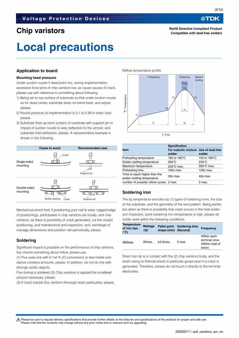
Application to board
Mounting head pressureUnder suction nozzle if dead point too, during implementation, excessive force joins of chip varistors low, as cause causes of crack, please use with reference to something about following.1) Being set to top surface of substrate so that under suction nozzle
as for dead center, substrate does not bend back, and adjust, please.
2) Nozzle pressure at implementation is 0.1 to 0.3N in static load, please.
3) Substrate fixes up back surface of substrate with support pin in impact of suction nozzle to wely deflection to the utmost, and substrate hold deflection, please. A representative example is shown in the following.
Mechanical shock that, if positioning your nail to wear, ragged edge of positionings, participates in chip varistors are locally, and chip varistors, as there is possibility of crack generated, cut the closed positioning, and maintenance and inspection, and, exchange of manage dimensions and position nail periodically, please.
Soldering
Significant impact is possible on the performance of chip varistors, flux checks something about follow, please use.(1) Flux uses one with 0.1wt % (Cl conversion) or less halide sub-stance contains amounts, please. In addition, do not do this with strongly acidic objects.Flux during is soldered (2) Chip varistors is applied the smalleset amount necessary, please.(3) If Used soluble flux, perform thorough wash particularly, please.
Reflow temperature profile
Soldering iron
The tip temperature and also by (1) types of soldering irons, the size of the substrate, and the geometry of the land pattern. Being earlier, but when as there is possibility that crack occurs in the heat ander-son impaction, point soldering iron temperature is high, please do solder work within the following conditions.
Direct iron tip is in contact with the (2) chip varistors body, and the strain owing to thermal shock in particular grows even if a crack is generated. Therefore, please do not touch it directly to the terminal electrodes.
Local precautions
RoHS Directive Compliant ProductCompatible with lead-free solders
Cases to avoid Recommended case
Single-sided mounting
Double-sided mounting
Crack
Support pin
Solder peeling Crack Support pin
ItemSpecificationFor eutectic mixture solder
Use of lead-free solder
Preheating temperature 160 to 180°C 150 to 180°CSolder melting temperature 200°C 230°CMaximum temperature 240°C max. 260°C max.Preheating time 100s max. 120s max.Time to reach higher than the solder melting temperature
30s max. 40s max.
number of possible reflow cycles 2 max. 2 max.
Temperatureof iron tips(°C)
Wattage(W)
Pallet point shape (mm)
Soldering time(Second)
Frequency
350max. 30max. ø3.0max. 5 max.
Within each terminal once(Within total of twice)
Naturalcooling
t3
t1
Preheating
t2
Soldering
T3 T3
T4
T2
T1
t: Time
Peak
T: T
empe
ratu
re

(10/12)
20200217 / vpd_varistors_avr_en.fm
Please be sure to request delivery specifications that provide further details on the features and specifications of the products for proper and safe use.Please note that the contents may change without any prior notice due to reasons such as upgrading.
V o l t a g e P r o t e c t i o n D e v i c e s
Chip varistors
Cleaning
(1) If cleaning liquid is inappropriate, residues and other foreign body of fluxes builds up on chip varistors, and can degrade the per-formance of chip varistors (particularly the insulation resistance).(2) Wash conditions may compromise performance of chip varistors if they are improper (wash due, wash excess).
2-1) For wash due (a) By substance of a system in flux residue halide, metal including
terminal electrodes may experience corrosion. (b) Substance of a system in flux residue halide builds up on chip
varistors, and reduces the insulation resistance.(c) Soluble flux makes comparisons of colophony series flux, and
there is event with trends of significant (1) and(2).
2-2) For excess wash(1) Owing to lavage, chip varistors deteriorates, and reduces perfor-
mance of chip varistors.(2) In ultrasonography, when output is passed, substrate resonates
size, and crack occurs in body and sprang of chip varistors in vibration of substrate. Since this may reduce the strength of the terminal electrode, please note the following conditions. [Please review the italicized portion, as I am unsure what you mean to convey here.]
Ultrasound outputUltrasonic frequencyUltrasound cleaning time
2-3) Concentration including halogen that when cleaning liquid to pollution, when you released is higher, and may cause similar of results into wash due.
Substrate handling after component mounting
(1) When substrate is divided, a flexible so that show in following dia-gram to substrate, and is given by stress including twist, as there is possibility that crack occurs of chip varistors, please check that stress is within acceptable limits.
(2) During each substrate operational check, push pressure with contact failure of check pin of boards checkers of check pin may be toned up to be prevented. As substrate is bent under loading, chip varistors is broken owing to stress. There is also the possibility that solder on the terminal electrode will peel off. Follow the diagram for reference, and check that the substrate bends, please.
Single-part component handling
To drop impact, as there is possibility that breakage and crack is
entered, do not chip varistors that(1) chip varistors falls.
(2) At stacking storage after implementation and treatment of sub-
strate, corner of boards is regarded as chip varistors. Please be
careful, as there is the possibility that breakage and cracks will
occur on impact.
Attention after implementation
RoHS Directive Compliant ProductCompatible with lead-free solders
Bends Twist
Item Cases to avoid Recommended case
Substrate sags
Peeling
Check pin Check pin
Support pin
Floor
Crack
BoardCrack
(11/12)
20200217 / vpd_varistors_avr_en.fm
Please be sure to request delivery specifications that provide further details on the features and specifications of the products for proper and safe use.Please note that the contents may change without any prior notice due to reasons such as upgrading.
V o l t a g e P r o t e c t i o n D e v i c e s
Chip varistors
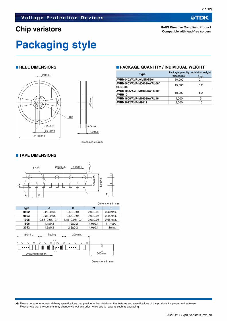
REEL DIMENSIONS PACKAGE QUANTITY / INDIVIDUAL WEIGHT
TAPE DIMENSIONS
Packaging style
RoHS Directive Compliant ProductCompatible with lead-free solders
ø180±2.0
2.0±0.5
ø13±0.2
ø21±0.8
Dimensions in mm
0.8
ø60
min
.
14.0max.
9.0max.
TypePackage quantity Individual weight
(pieces/reel) (mg)AVRM0402/AVRL04/SNGE04 20,000 0.1AVRM0603/AVR-M0603/AVRL06/SGNE06
15,000 0.2
AVRM1005/AVR-M1005/AVRL10/AVRH10
10,000 1.2
AVRM1608/AVR-M1608/AVRL16 4,000 5AVRM2012/AVR-M2012 2,000 13
Dimensions in mm
Type A B P1 T0402 0.26±0.04 0.46±0.04 2.0±0.05 0.40max.0603 0.38±0.05 0.68±0.05 2.0±0.05 0.45max.1005 0.65+0.05/–0.1 1.15+0.05/–0.1 2.0±0.05 0.65max.1608 1.1±0.2 1.9±0.2 4.0±0.1 1.1max.2012 1.5±0.2 2.3±0.2 4.0±0.1 1.1max
4.0±0.12.0±0.05
B
A P1
8.0±
0.3
1.75
±0.
1
3.5±
0.05
T
1.5 +0.10
Dimensions in mm
160min. Taping 200min.
300min.Drawing direction
(12/12)
20200217 / vpd_varistors_avr_en.fm
Please be sure to request delivery specifications that provide further details on the features and specifications of the products for proper and safe use.Please note that the contents may change without any prior notice due to reasons such as upgrading.
V o l t a g e P r o t e c t i o n D e v i c e s
REMINDERS FOR USING THESE PRODUCTSBefore using these products, be sure to request the delivery specifications.
SAFETY REMINDERSPlease pay sufficient attention to the warnings for safe designing when using this products.
Please pay careful attention to the precautions and follow safe designing practices when using these products.
Please observe the following precautions in order to avoid problems with chip varistors such as characteristic degradation and element
destruction
Please store these products in an environment with a temperature of 5 to 40°C and humidity level of 20 to 70%RH, and use them
within six months.
Poor storage conditions may lead to the deterioration of the solderability of the edge electrodes, so please be careful to avoid contact
with humidity, dew condensation, dust, toxic gas (hydrogen, hydrogen sulfide, sulfurous acid, chlorine, ammonia, etc.), direct sunlight,
and so on.
Please do not use products that have been dropped or detached when mounting.
Please solder with the reflow soldering method, and not the flow (dip) soldering method.
Please observe the following precautions to avoid problems with varistors such as characteristic degradation and element destruction,
which ultimately lead to the generation of heat and smoke with the elements.Do not use in locations where the temperatures exceed the operating temperature range such as under direct sunlight or near
sources of heat.
Do not use in locations where there are high levels of humidity such as under direct exposure to weather and areas where steam is
released.
Do not use in locations such as dusty areas, high-saline environments, places where the atmosphere is contaminated with corrosive
gas, etc.
Avoid powerful vibrations, impact (such as by dropping), pressure, etc. that may lead to splitting in the products.
Do not use with a voltage that exceeds the maximum allowable circuit voltage.When resin coating (including modular) a varistor, do not use a resin that will cause deterioration of the varistor. Be sure never to use
resin that generates hydrogen as palladium is used for the inner electrode.
Avoid attachment near combustible materials.
Please contact our sales offices when considering the use of the products listed on this catalog for applications, whose performance
and/or quality require a more stringent level of safety or reliability, or whose failure, malfunction or trouble could cause serious damage
to society, person or property ('specific uses' such as automobiles, airplanes,medical instruments, nuclear devices, etc.) as well as
when considering the use for applications that exceed the range and conditions of this catalog.
Please also contact us when using these products for automotive applications.
As range of catalog, conditions are transcended, or for damage that generated by was used in application specific, etc, accept no the
responsibility, wish.
Please take appropriate measures such as acquiring protective circuits and devices that meet the uses, applications, and conditions of
the instruments and keeping backup circuits.
REMINDERS