CHAPTER 2 (CONTD.)
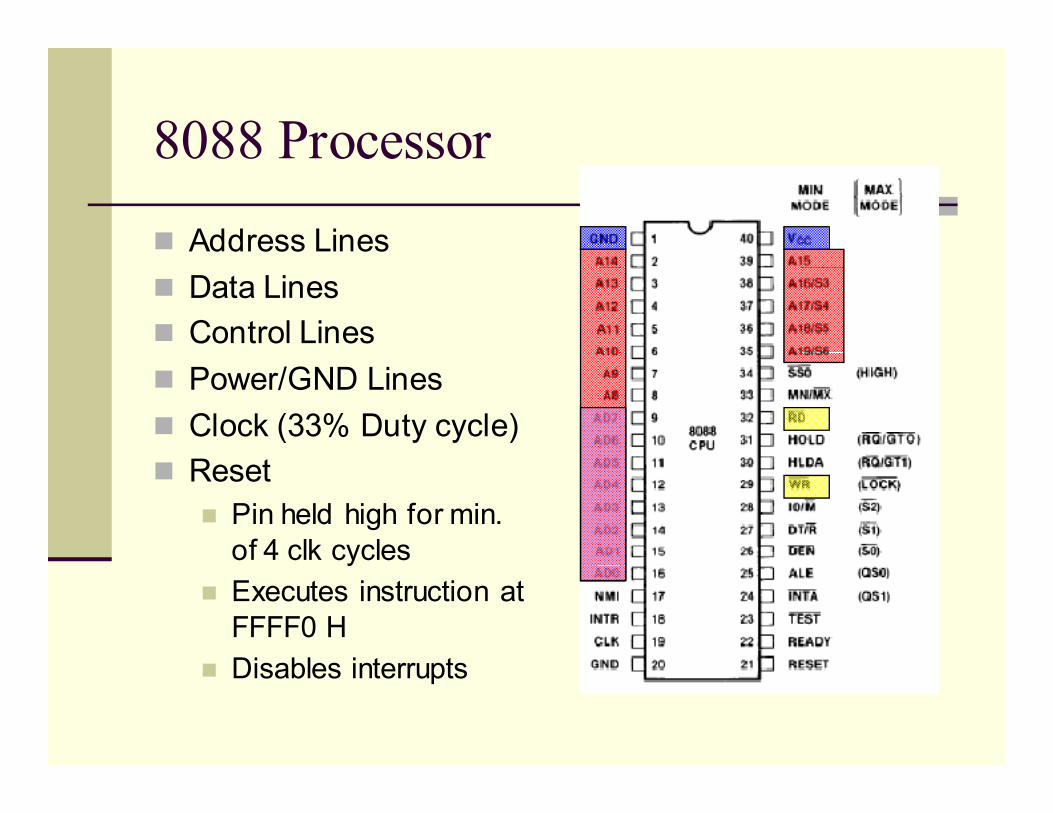
8088 Processor
� Address Lines
� Data Lines
� Control Lines
� Power/GND Lines
� Clock (33% Duty cycle)
� Reset
� Pin held high for min.
of 4 clk cycles
� Executes instruction at
FFFF0 H
� Disables interrupts
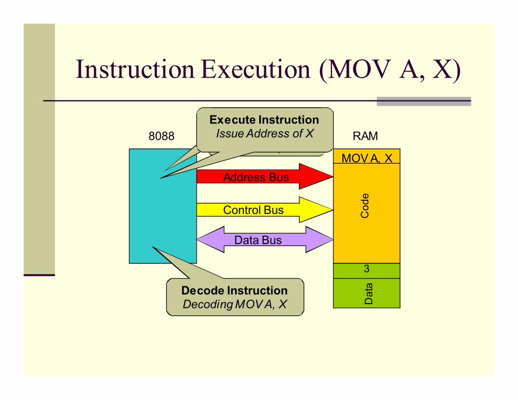
Instruction Execution (MOV A, X)
8088 RAM
Address Bus
Co
de
MOV A, X
Data Bus
Da
ta
3
Fetch Instruction
Issue Address of
MOV A, X
Control Bus
Decode Instruction
Decoding MOV A, X
Execute Instruction
Issue Address of X

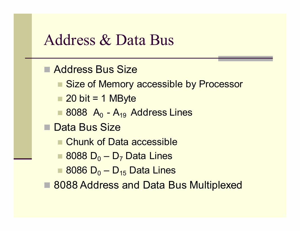
Address & Data Bus
� Address Bus Size
� Size of Memory accessible by Processor
� 20 bit = 1 MByte
� 8088 A0 - A19 Address Lines
� Data Bus Size
� Chunk of Data accessible
� 8088 D0 – D7 Data Lines
� 8086 D0 – D15 Data Lines
� 8088 Address and Data Bus Multiplexed
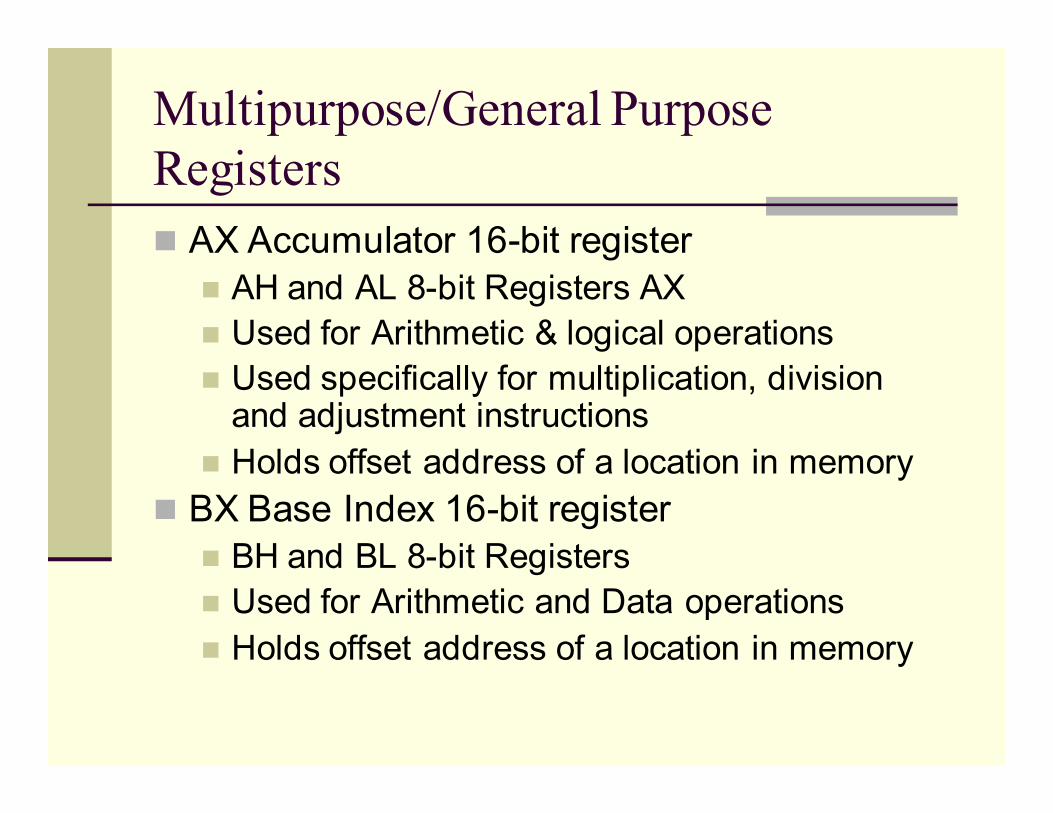
Multipurpose/General Purpose
Registers
� AX Accumulator 16-bit register
� AH and AL 8-bit Registers AX
� Used for Arithmetic & logical operations
� Used specifically for multiplication, division and adjustment instructions
� Holds offset address of a location in memory
� BX Base Index 16-bit register
� BH and BL 8-bit Registers
� Used for Arithmetic and Data operations
� Holds offset address of a location in memory
Multipurpose/General Purpose
Registers
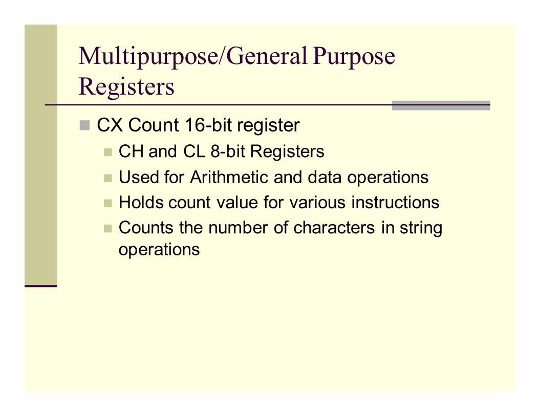
� CX Count 16-bit register
� CH and CL 8-bit Registers
� Used for Arithmetic and data operations
� Holds count value for various instructions
� Counts the number of characters in string
operations
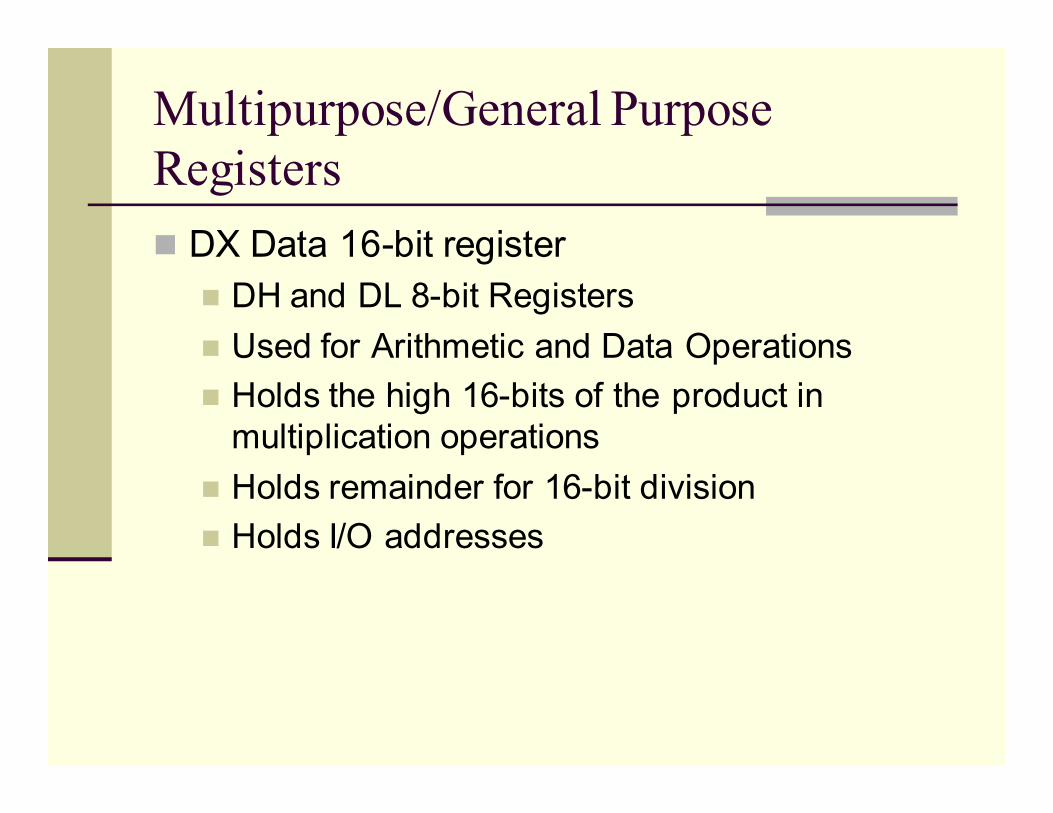
Multipurpose/General Purpose
Registers
� DX Data 16-bit register
� DH and DL 8-bit Registers
� Used for Arithmetic and Data Operations
� Holds the high 16-bits of the product in
multiplication operations
� Holds remainder for 16-bit division
� Holds I/O addresses

Base Registers
� Base Pointer BP 16-bit Register
� Points to a memory location
� Holds an offset or displacement from Stack Segment (SS) Register
� Used by subroutines to locate variables passed on stack by calling program
� BX Base Index 16-bit register
� BH and BL 8-bit Registers
� Used for Arithmetic and Data operations
� Holds offset address of a location in memory

Index Registers
� Destination Index DI 16-bit Register
� Addresses string destination for string
instructions
� Holds an offset or displacement from ES
register
� Source Index SI 16-bit Register
� Addresses string source for string instructions
� Holds an offset or displacement from DS
register

Stack Pointer Registers
� Stack Pointer SP 16-bit Register
� Addresses Stack memory
� Holds an offset or displacement from SS
Register
� Contents are combined with contents of SS
Register to give address of top of stack
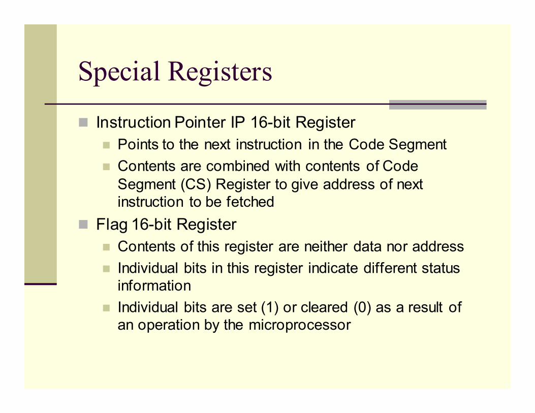
Special Registers
� Instruction Pointer IP 16-bit Register
� Points to the next instruction in the Code Segment
� Contents are combined with contents of Code
Segment (CS) Register to give address of next
instruction to be fetched
� Flag 16-bit Register
� Contents of this register are neither data nor address
� Individual bits in this register indicate different status
information
� Individual bits are set (1) or cleared (0) as a result of
an operation by the microprocessor
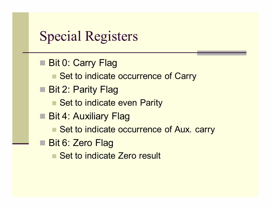
Special Registers
� Bit 0: Carry Flag
� Set to indicate occurrence of Carry
� Bit 2: Parity Flag
� Set to indicate even Parity
� Bit 4: Auxiliary Flag
� Set to indicate occurrence of Aux. carry
� Bit 6: Zero Flag
� Set to indicate Zero result
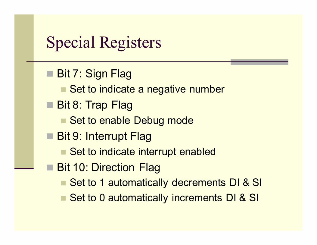
Special Registers
� Bit 7: Sign Flag
� Set to indicate a negative number
� Bit 8: Trap Flag
� Set to enable Debug mode
� Bit 9: Interrupt Flag
� Set to indicate interrupt enabled
� Bit 10: Direction Flag
� Set to 1 automatically decrements DI & SI
� Set to 0 automatically increments DI & SI
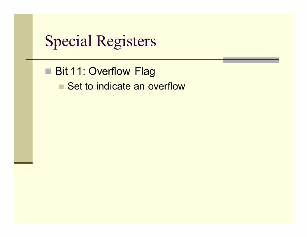
Special Registers
� Bit 11: Overflow Flag
� Set to indicate an overflow

Chapter 3
� 8086 microprocessor
� Internal registers
� Making of Memory address
� Number conversion

Instruction Execution (MOV A, X)
8088 RAM
Address Bus
Co
de
MOV A, X
Data Bus
Da
ta
3
Fetch Instruction
Issue Address of
MOV A, X
Control Bus
Decode Instruction
Decoding MOV A, X
Execute Instruction
Issue Address of X
Address & Data Bus
� Address Bus Size
� Size of Memory accessible by Processor
� 20 bit = 1 MByte
� 8088 A0 - A19 Address Lines
� Data Bus Size
� Chunk of Data accessible
� 8088 D0 – D7 Data Lines
� 8086 D0 – D15 Data Lines
� 8088 Address and Data Bus Multiplexed

8088 Processor
� Address Lines
� Data Lines
� Control Lines
� Power/GND Lines
� Clock (33% Duty cycle)
� Reset
� Pin held high for min.
of 4 clk cycles
� Executes instruction at
FFFF0 H
� Disables interrupts

Lecture 02 20
DC Characteristics
� Input Characteristics
� Input current and voltage requirements
� Logic 0 0.8 Vmax ±10 µAmax
� Logic 1 2 Vmin ±10 µAmax
� Inputs gate connections of MOSFETs
� Leakage currents
Lecture 02 21
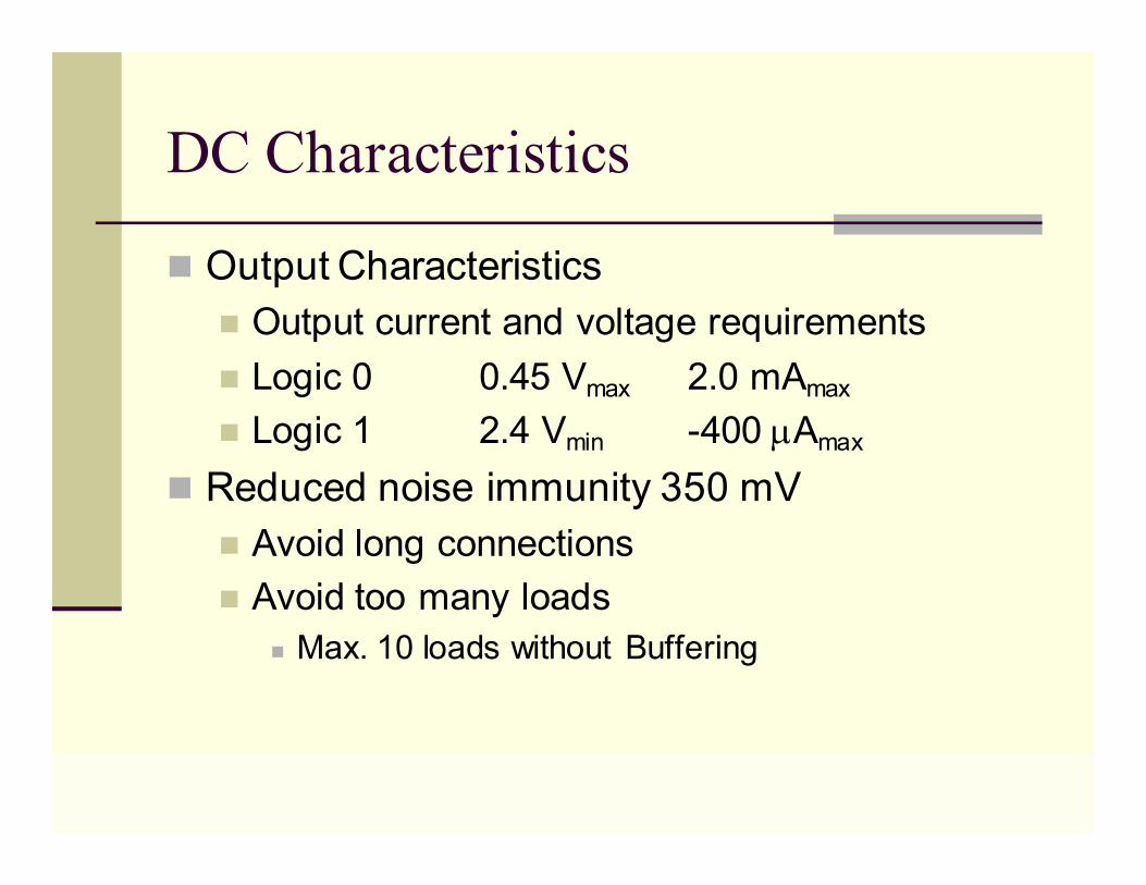
DC Characteristics
� Output Characteristics
� Output current and voltage requirements
� Logic 0 0.45 Vmax 2.0 mAmax
� Logic 1 2.4 Vmin -400 µAmax
� Reduced noise immunity 350 mV
� Avoid long connections
� Avoid too many loads
� Max. 10 loads without Buffering
Lecture 02 22
Bus Buffering & Latching
� Bus should be buffered for large systems
� Multiplexed Address & Data Buses should be
De-multiplexed
� Why De-multiplexed Buses?
� Address on the Address Bus has to remain
constant throughout a read and write cycle
� Read and Write Cycle?
� 8088/8086 read/write operation is completed
in a minimum period of 4 clocks
Lecture 02 23
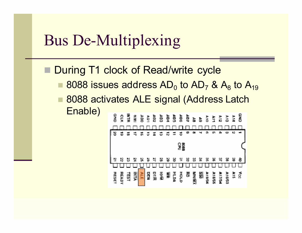
Bus De-Multiplexing
� During T1 clock of Read/write cycle
� 8088 issues address AD0 to AD7 & A8 to A19
� 8088 activates ALE signal (Address Latch
Enable)
Lecture 02 24
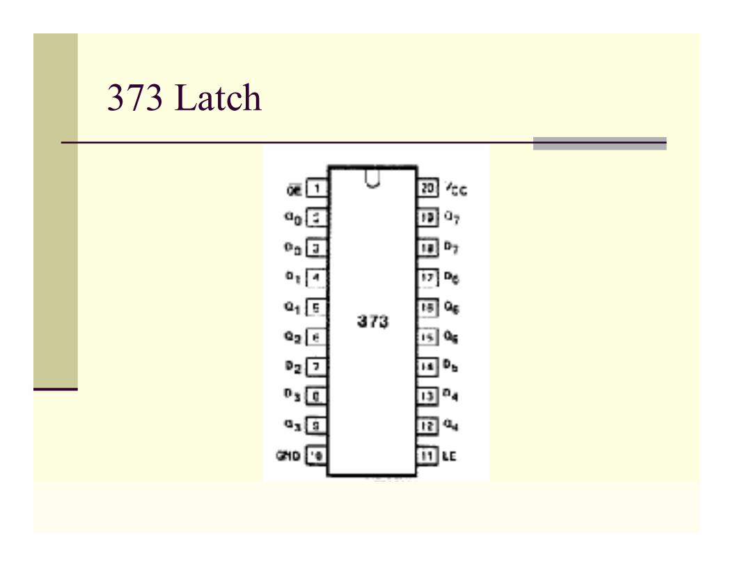
373 Latch
Lecture 03 25
Bus Buffering
� Address Lines A0 – A19 have to be buffered
� A0 – A7 & A16 – A19 have been buffered by 373
� Logic 0 sinks 32 mA
� Logic 1 sources 5.2 mA
� A8 – A15 have to be buffered
� 74LS244 Octal Buffer used for Buffering

De-multiplexed Bus
8088
AD0 – AD7
373 Latch
373
A0 – A7
A8 – A15
A16 – A19
ALELE
LE
GND
GND
OE*
OE*
D0 – D7
Lecture 03 27
Clock Circuitry
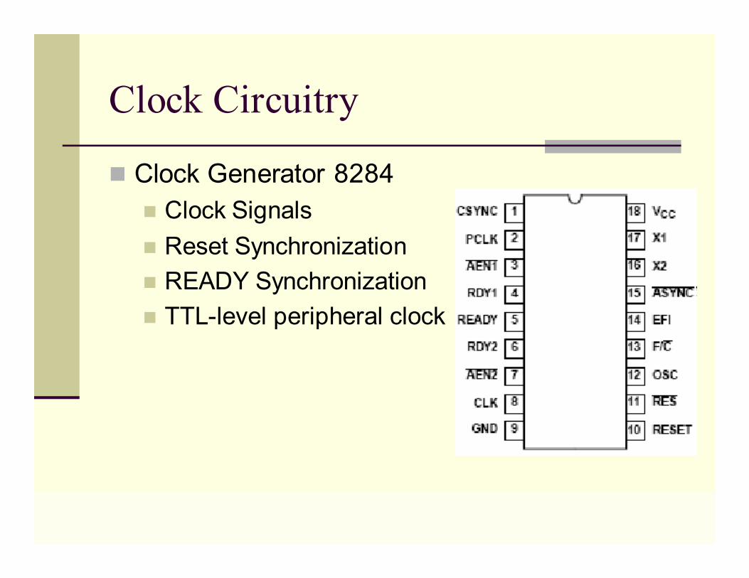
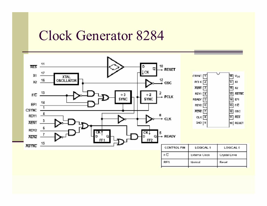
� Clock Generator 8284
� Clock Signals
� Reset Synchronization
� READY Synchronization
� TTL-level peripheral clock
Lecture 04 28
Clock Generator 8284
Lecture 04 29
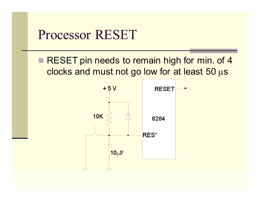
Processor RESET
� RESET pin needs to remain high for min. of 4
clocks and must not go low for at least 50 µs

Lecture 04 30
Bus Timing
� Memory & I/O is slow
� Rate of data transfer depends on access time
of Memory & I/O
� Processor Read/Write cycles have to be
extended to allow transfer from slow devices
� Basic Bus Operation
� Address, Data and Control Buses are
involved in reading and writing of data
� Address, Data and Control Bus operations are
carried out in a sequence

Lecture 04 31
Bus Timing
� 8086/8088 use the Memory/IO in periods
called Bus Cycles
� Each Bus Cycle equals 4 system clocking
periods (T states)
� Pentium has 2 T state Bus cycle
� At 5 MHz, one Bus cycle is completed at 0.8
µsec or 800 nsec
� Processor can read/write at a max. rate of
1.25 million times a sec.
Lecture 04 32
Bus Timing
� With internal queue processor can execute
2.5 million instructions per sec. [MIPS] in
bursts
� Pentium operates at much higher rates due to
higher clock rates, shorter Bus cycle and
internal queuing

Lecture 04 33
Bus Timing T1 Clock
� Address of the Memory/IO is issued via the
Address/Data Multiplexed Bus
� Following Signals are also issued
� ALE Address Latch Enable signal
� DT/R* Data Transmit/Receive signal
� IO/M* IO/Memory signal
Lecture 04 34
Bus Timing T2 & T3 Clocks
� RD* or WR* Read or Write Signal is issued
� Incase of Write the Data to be written also appears on the Data Bus
� DEN* Data Bus Enable signal is issued
� READY signal is sampled at the end of T2
� If READY is low T3 becomes a Wait State TW
� READY is again sampled in the middle of Wait State
� If the Bus Cycle is Read Cycle, Data Bus is sampled at the end of T3
Lecture 04 35
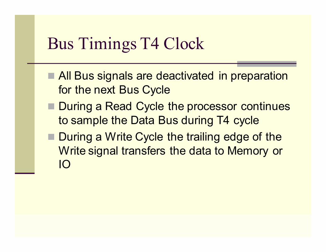
Bus Timings T4 Clock
� All Bus signals are deactivated in preparation
for the next Bus Cycle
� During a Read Cycle the processor continues
to sample the Data Bus during T4 cycle
� During a Write Cycle the trailing edge of the
Write signal transfers the data to Memory or
IO
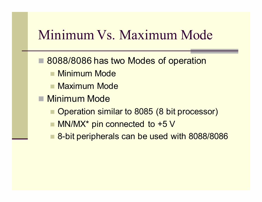
Minimum Vs. Maximum Mode
� 8088/8086 has two Modes of operation
� Minimum Mode
� Maximum Mode
� Minimum Mode
� Operation similar to 8085 (8 bit processor)
� MN/MX* pin connected to +5 V
� 8-bit peripherals can be used with 8088/8086
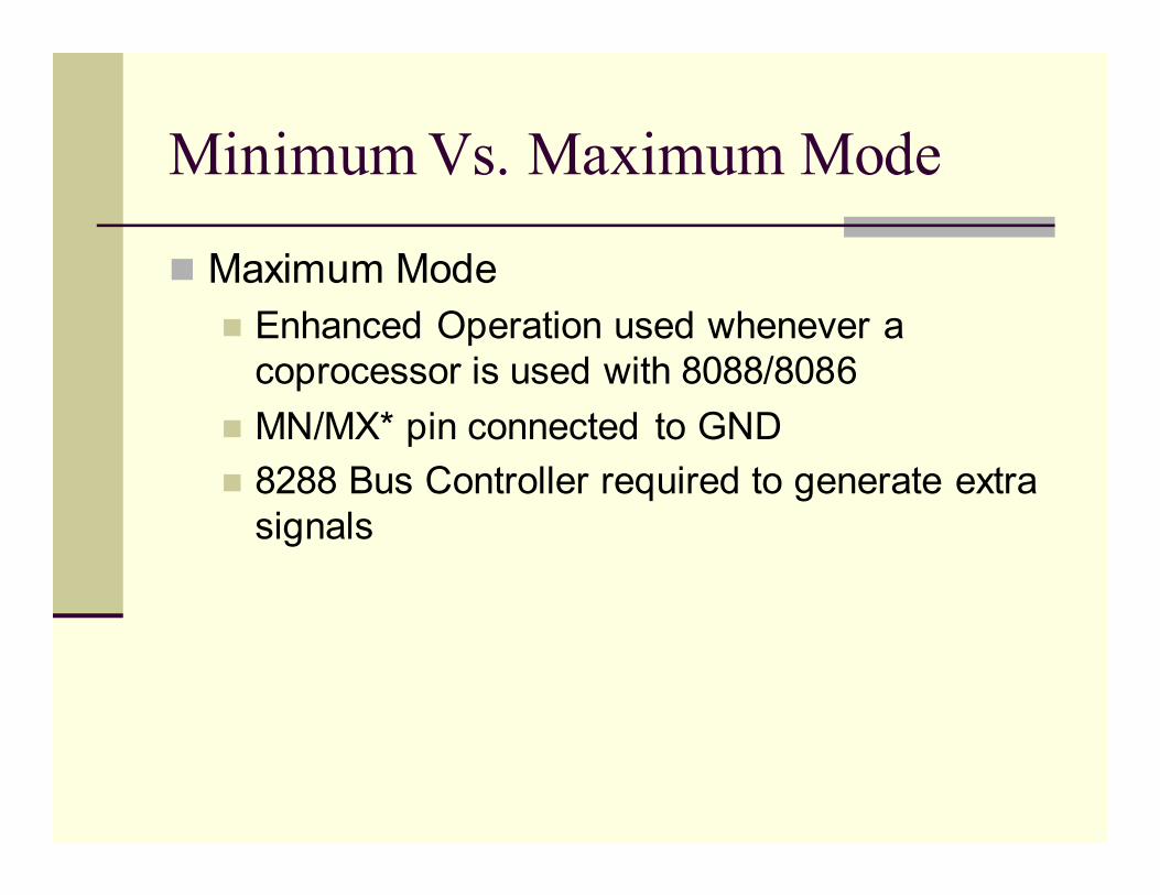
Minimum Vs. Maximum Mode
� Maximum Mode
� Enhanced Operation used whenever a
coprocessor is used with 8088/8086
� MN/MX* pin connected to GND
� 8288 Bus Controller required to generate extra
signals
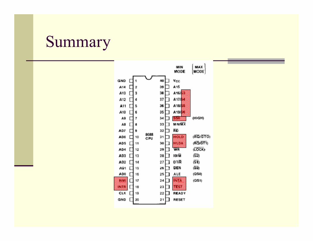
Summary
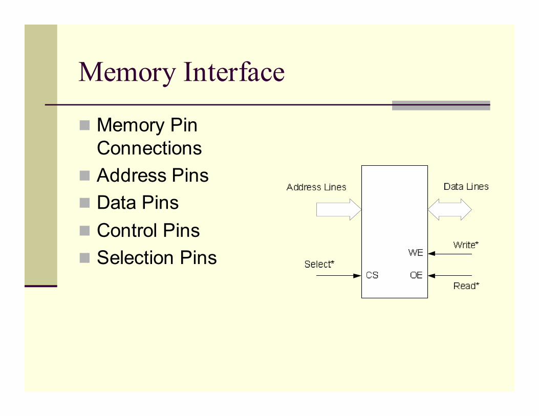
Memory Interface
� Memory Pin
Connections
� Address Pins
� Data Pins
� Control Pins
� Selection Pins
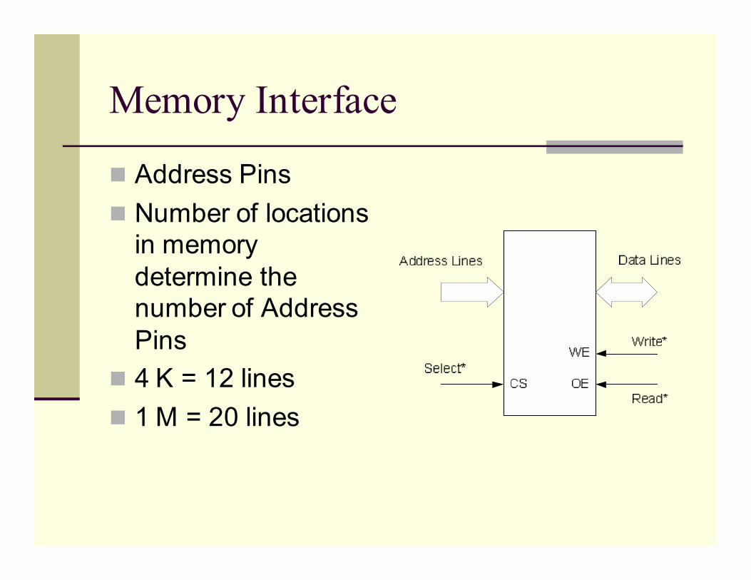
Memory Interface
� Address Pins
� Number of locations
in memory
determine the
number of Address
Pins
� 4 K = 12 lines
� 1 M = 20 lines
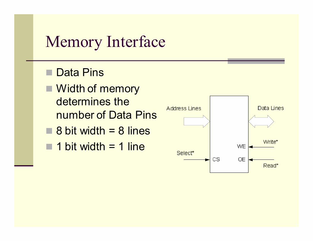
Memory Interface
� Data Pins
� Width of memory
determines the
number of Data Pins
� 8 bit width = 8 lines
� 1 bit width = 1 line

Memory Interface
� ROM Control Pins
� OE* or G* allows
data to flow out
� RAM Control Pins
� WE* allows data to
be written
� OE*allows data to
be read
� Can have a single
R/W* pin

Memory Interface
� Selection Pins
� CE* or CS* allows
the RAM/ROM chip
to be selected
� Sometimes there
are more than one
CS* signal
ROM
� Read Only ROM
� Permanently stores program/data
� Does not allow write (read Only)

2764 (8 KB) EPROM
Address Decoding
� Processors have very large address space
� Pentium 4 has a 64 GB memory space
� Entire memory space is not used
� Processor memory space is used for specific
purpose
� Operating System
� Program Code
� Data
� Interrupt Vector Table
Address Decoding
� RAM, ROM and I/O devices are mapped in
the processor memory space
� More memory can be added in the vacant
memory space
Memory Mapping
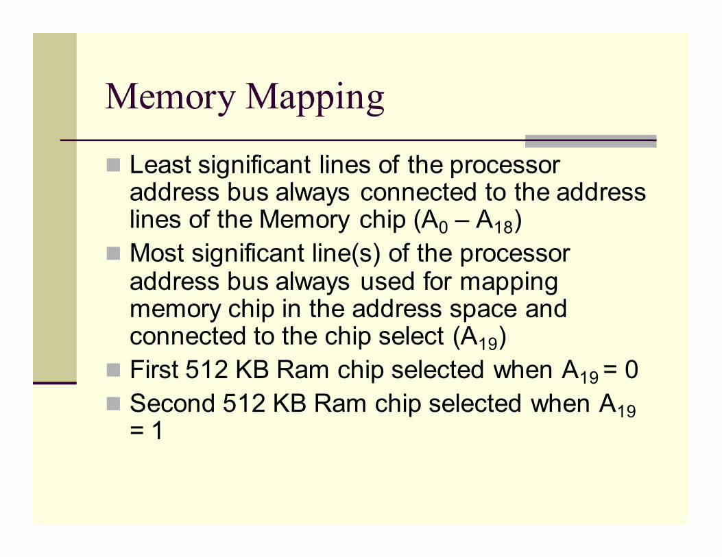
� Least significant lines of the processor address bus always connected to the address lines of the Memory chip (A0 – A18)
� Most significant line(s) of the processor address bus always used for mapping memory chip in the address space and connected to the chip select (A19)
� First 512 KB Ram chip selected when A19 = 0
� Second 512 KB Ram chip selected when A19
= 1

Memory Mapping

Memory Mapping
� 256 KB RAM chip (A0 – A17)
� Four 256 KB RAM chips should be connected
to completely map the 1 MB processor
memory space
� Address Lines A18 & A19 used for chip
selection

Gate Decoder
� 1st 256 KB RAM chip selected when A19 = 0 & A18 = 0
� A two input OR gate
� 2nd 256 KB RAM chip selected when A19 = 0 & A18 = 1
� A two input OR gate with A18 input inverted
� 3rd 256 KB RAM chip selected when A19 = 1 & A18 = 0
� A two input OR gate with A19 input inverted
� 4th 256 KB RAM chip selected when A19 = 1 & A18 = 1
� A two input NAND gate

Lecture 08 52
Designing Address Decoders
� Flexible Design
� can be easily modified
� Allow for future expansion
� Should introduce minimum gate delay
� Low chip count
Lecture 08 53
Address Decoding
� Full Address Decoding
� Entire address space is fully decoded
� More decoding circuitry is required
� Partial Address Decoding
� Address space is not fully decoded
� Less decoding circuitry is required
� Address clashes occur
� Block Address Decoding
� Memory space divided into blocks of equal sizes
Lecture 08 54
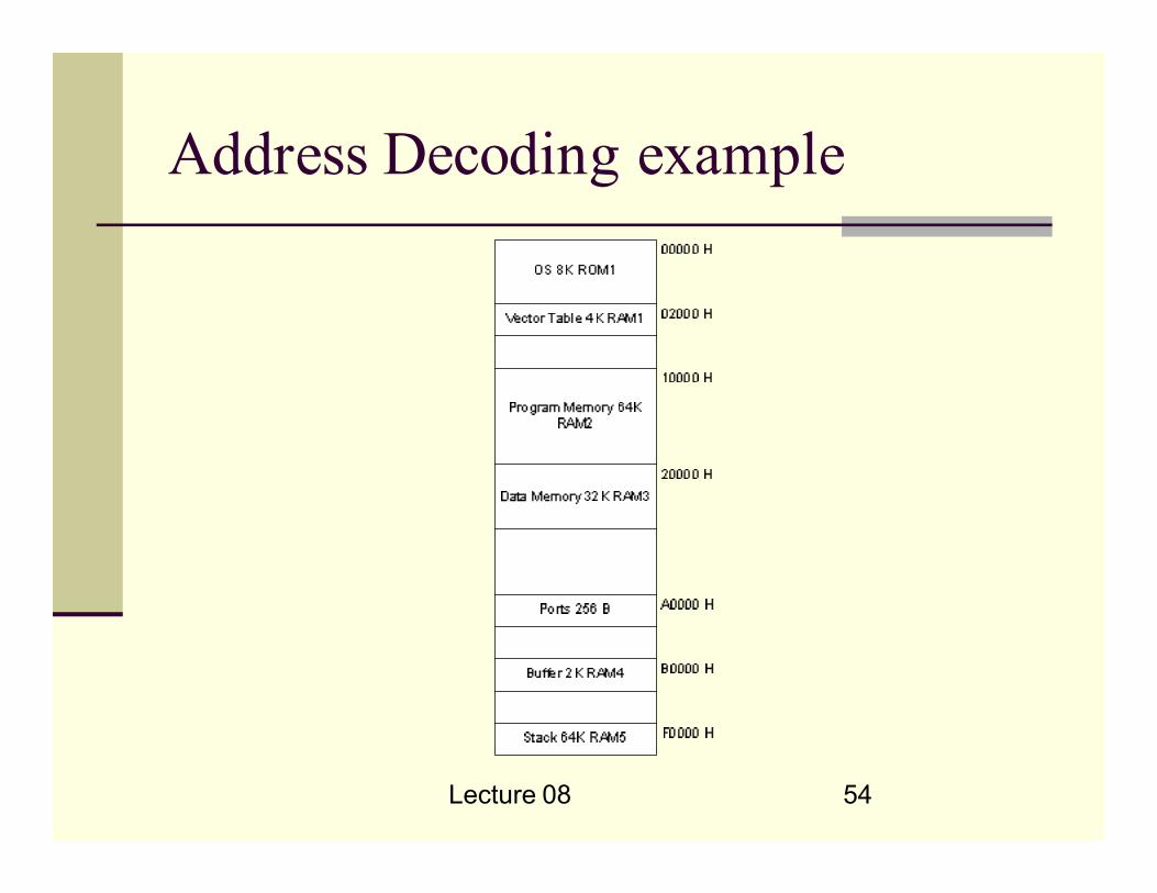
Address Decoding example
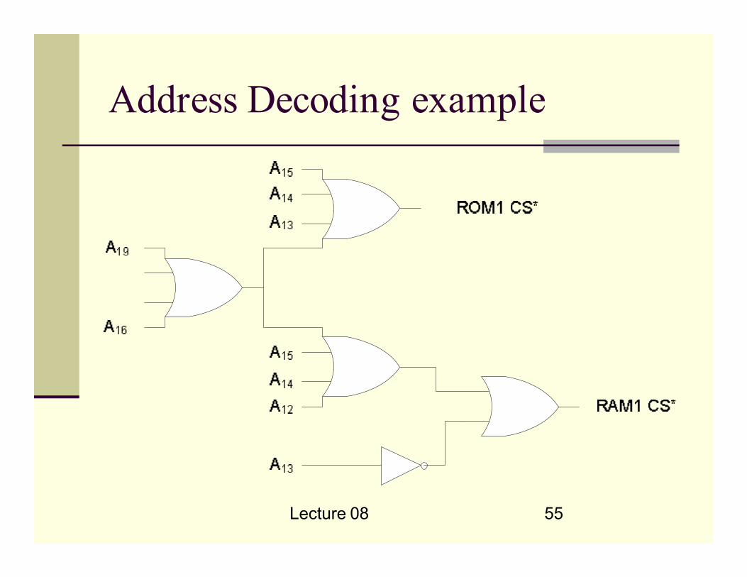
Lecture 08 55
Address Decoding example

Lecture 08 56
Address Decoding example

Lecture 08 57
Address Decoding example
Lecture 08 58
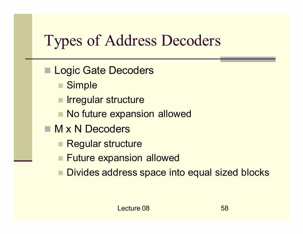
Types of Address Decoders
� Logic Gate Decoders
� Simple
� Irregular structure
� No future expansion allowed
� M x N Decoders
� Regular structure
� Future expansion allowed
� Divides address space into equal sized blocks

Lecture 08 59
Types of Address Decoders
� ROM based Decoders
� Very flexible
� New decoding scheme implemented by
reprogramming the ROM
� PLDs based Decoders
� Very flexible have replaced PROM based
Decoders
Lecture 09 60
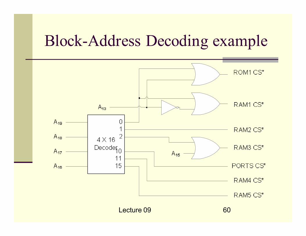
Block-Address Decoding example

Lecture 09 61
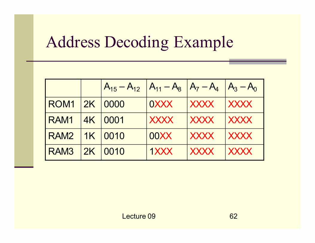
Address Decoding Example
� Map the memory chips in contiguous memory
locations starting from address 0000 H with
minimal empty slots
� 2K ROM1, 4K RAM1, 1K RAM2, 2K RAM3
� How should it be done?
� Start by sketching an Address Decoding Table
Lecture 09 62
Address Decoding Example
A15 – A12 A11 – A8 A7 – A4 A3 – A0
ROM1 2K 0000 0XXX XXXX XXXX
RAM1 4K 0001 XXXX XXXX XXXX
RAM2 1K 0010 00XX XXXX XXXX
RAM3 2K 0010 1XXX XXXX XXXX

Lecture 10 63
Types of Address Decoders
� Logic Gate Decoders
� Simple
� Irregular structure
� No future expansion allowed
� High chip count
� High decoding speed
Lecture 10 64
Types of Address Decoders
� M x N Decoders
� Regular structure
� Future expansion allowed
� Divides address space into equal sized blocks
� Low chip count
Lecture 10 65
Types of Address Decoders
� ROM based Decoders
� Very flexible
� New decoding scheme implemented by
reprogramming the ROM
� PLDs based Decoders
� Very flexible have replaced PROM based
Decoders
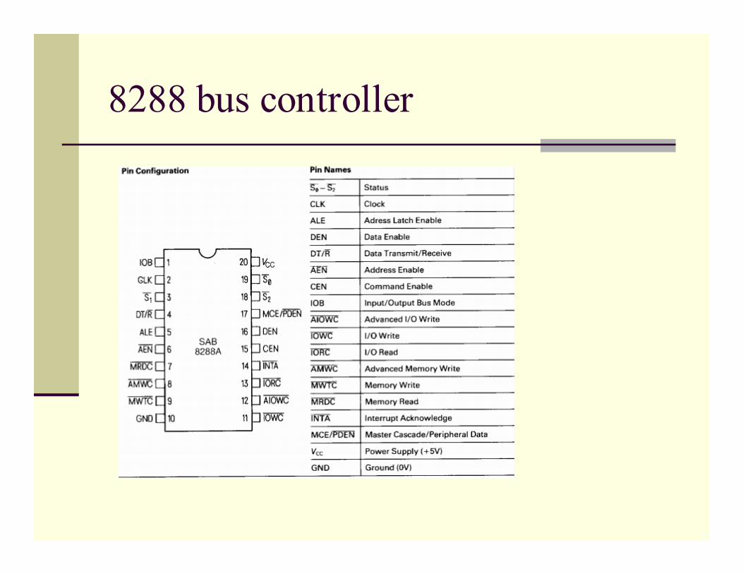
8288 bus controller
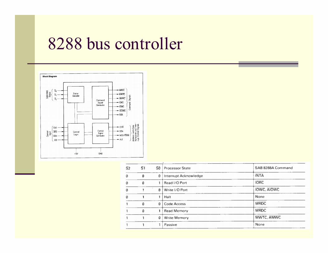
8288 bus controller

8155 chip


![KSZ9692PB ds r50 091311a - Microchip Technology...E1, E2, E3 SADDR[23..0] O SRAM Address Bus. The 24-bit address bus covers 16M word memory space of ROM/SRAM/FLASH, and 16M byte external](https://static.cupdf.com/doc/110x72/60c173a8f251cc06833b7903/ksz9692pb-ds-r50-091311a-microchip-technology-e1-e2-e3-saddr230-o-sram.jpg)