GB
CLASS 1LASER PRODUCT
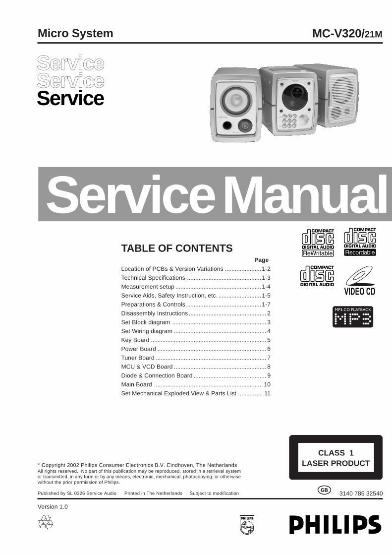
ServiceServiceServiceServiceService
MC-V320/21M
TABLE OF CONTENTSPage
Location of PCBs & Version Variations ......................1-2
Technical Specifications .............................................1-3
Measurement setup ....................................................1-4
Service Aids, Safety Instruction, etc. ..........................1-5
Preparations & Controls .............................................1-7
Disassembly Instructions ............................................... 2
Set Block diagram ......................................................... 3
Set Wiring diagram ........................................................ 4
Key Board ...................................................................... 5
Power Board .................................................................. 6
Tuner Board ................................................................... 7
MCU & VCD Board ........................................................ 8
Diode & Connection Board ............................................ 9
Main Board .................................................................. 10
Set Mechanical Exploded View & Parts List ............... 11
© Copyright 2002 Philips Consumer Electronics B.V. Eindhoven, The NetherlandsAll rights reserved. No part of this publication may be reproduced, stored in a retrieval systemor transmitted, in any form or by any means, electronic, mechanical, photocopying, or otherwisewithout the prior permission of Philips.
Published by SL 0326 Service Audio Printed in The Netherlands Subject to modification
Micro System
3140 785 32540
Version 1.0
Service Manual
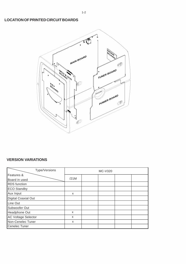
1-2
LOCATION OF PRINTED CIRCUIT BOARDS
VERSION VARIATIONS
Type/Versions MC-V320Features &
Board in usedRDS function
Aux Input
ECO Standby
Digital Coaxial Out
x
Subwoofer Out
Line Out
Headphone Out
/21M
AC Voltage Selector x
Non-Cenelec TunerCenelec Tuner
x
x
MAIN BOARD
TUNER BOARD
POWER BOARD
MCU & VCD
BOARD
KEYBOARD
DIODE
BOARD
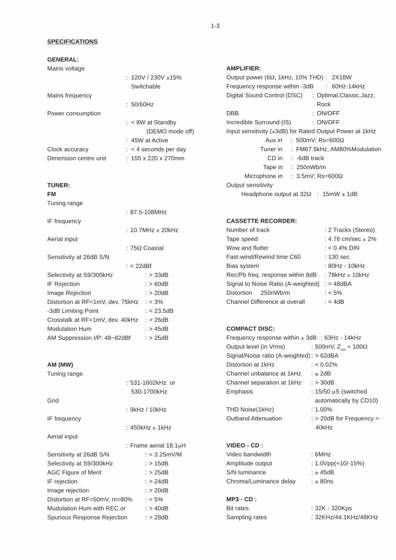
1-3
SPECIFICATIONS
GENERAL:
Mains voltage
: 120V / 230V ±15%
Switchable
Mains frequency
: 50/60Hz
Power consumption
: < 8W at Standby
(DEMO mode off)
: 45W at Active
Clock accuracy : < 4 seconds per day
Dimension centre unit : 155 x 220 x 270mm
TUNER:
FM
Tuning range
: 87.5-108MHz
IF frequency
: 10.7MHz ± 20kHz
Aerial input
: 75Ω Coaxial
Sensitivity at 26dB S/N
: < 22dBf
Selectivity at S9/300kHz : > 33dB
IF Rejection : > 60dB
Image Rejection : > 20dB
Distortion at RF=1mV, dev. 75kHz : < 3%
-3dB Limiting Point : < 23.5dB
Crosstalk at RF=1mV, dev. 40kHz : > 26dB
Modulation Hum : > 45dB
AM Suppression I/P: 48~82dBf : > 25dB
AM (MW)
Tuning range
: 531-1602kHz or
530-1700kHz
Grid
: 9kHz / 10kHz
IF frequency
: 450kHz ± 1kHz
Aerial input
: Frame aerial 18.1µH
Sensitivity at 26dB S/N : < 3.25mV/M
Selectivity at S9/300kHz : > 15dB
AGC Figure of Merit : > 25dB
IF rejection : > 24dB
Image rejection : > 20dB
Distortion at RF=50mV, m=80% : < 5%
Mudulation Hum with REC or : > 40dB
Spurious Response Rejection : > 28dB
AMPLIFIER:
Output power (6Ω, 1kHz, 10% THD) : 2X18W
Frequency response within -3dB : 60Hz-14kHz
Digital Sound Control (DSC) : Optimal,Classic,Jazz,
Rock
DBB : ON/OFF
Incredible Surround (IS) : ON/OFF
Input sensitivity (±3dB) for Rated Output Power at 1kHz
Aux in : 500mV; Rs=600Ω
Tuner in : FM67.5kHz, AM80%Modulation
CD in : -6dB track
Tape in : 250nWb/m
Microphone in : 3.5mV; Rs=600Ω
Output sensitivity
Headphone output at 32Ω : 15mW ± 1dB
CASSETTE RECORDER:
Number of track : 2 Tracks (Stereo)
Tape speed : 4.76 cm/sec ± 2%
Wow and flutter : < 0.4% DIN
Fast-wind/Rewind time C60 : 130 sec
Bias system : 80Hz - 10kHz
Rec/Pb freq. response within 8dB : 78kHz ± 10kHz
Signal to Noise Ratio (A-weighted) : > 48dBA
Distortion 250nWb/m : < 5%
Channel Difference at overall : < 4dB
COMPACT DISC:
Frequency response within ± 3dB : 63Hz - 14kHz
Output level (in Vrms) : 500mV, Zout = 100Ω
Signal/Noise ratio (A-weighted) : > 62dBA
Distortion at 1kHz : < 0.02%
Channel unbalance at 1kHz : ≤ 2dB
Channel separation at 1kHz : > 30dB
Emphasis : 15/50 µS (switched
automatically by CD10)
THD Noise(1kHz) : 1.00%
Outband Attenuation : > 20dB for Frequency >
40kHz
VIDEO - CD :
Video bandwidth : 6MHz
Amplitude output : 1.0Vpp(+10/-15%)
S/N luminance : ≥ 45dB
Chroma/Luminance delay : ≤ 80ns
MP3 - CD :
Bit rates : 32K - 320Kps
Sampling rates : 32KHz/44.1KHz/48KHz
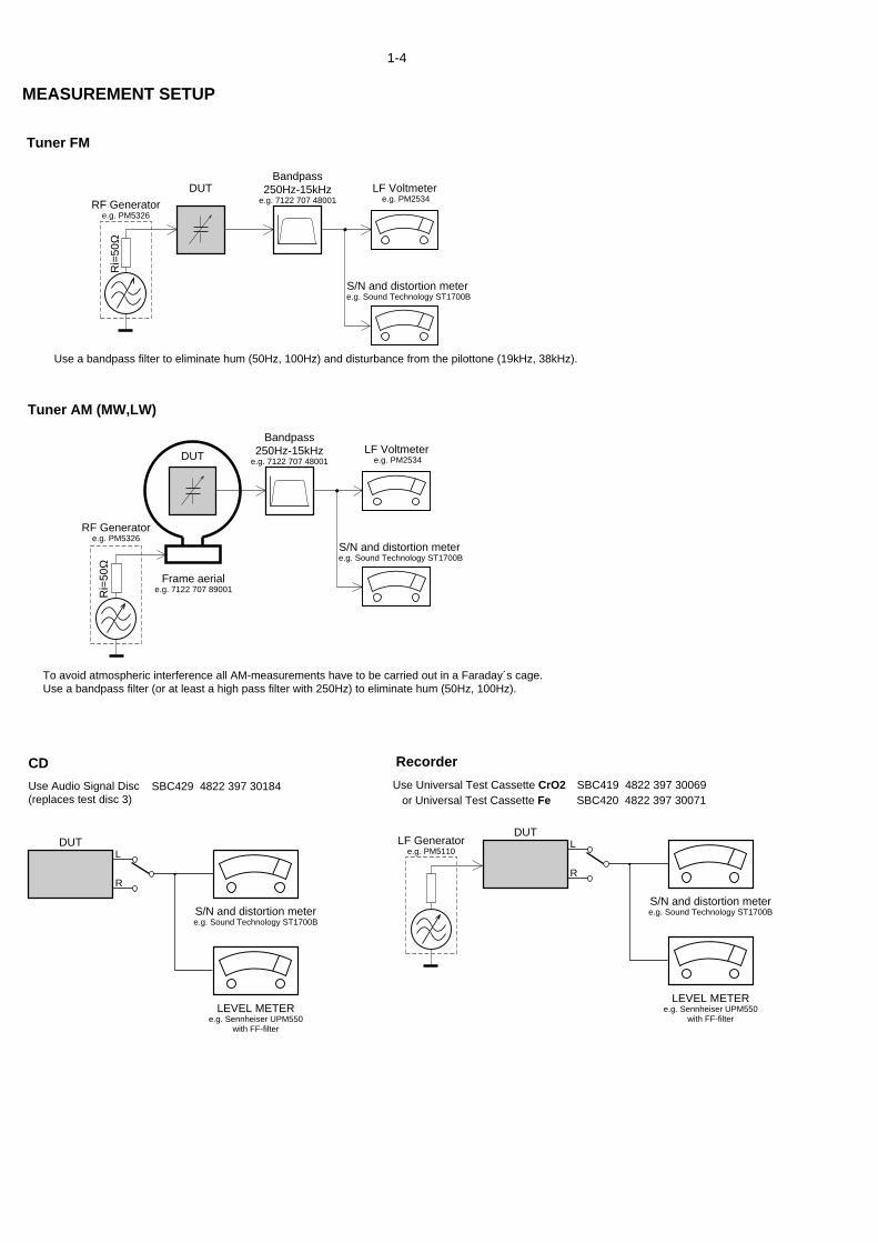
LF Generator e.g. PM5110
Recorder
Use Universal Test Cassette CrO2 SBC419 4822 397 30069
LEVEL METERe.g. Sennheiser UPM550
with FF-filter
S/N and distortion metere.g. Sound Technology ST1700B
L
R
DUT
or Universal Test Cassette Fe SBC420 4822 397 30071
LEVEL METERe.g. Sennheiser UPM550
with FF-filter
S/N and distortion metere.g. Sound Technology ST1700B
L
R
DUT
CD
Use Audio Signal Disc(replaces test disc 3)
SBC429 4822 397 30184
Bandpass250Hz-15kHz
e.g. 7122 707 48001LF Voltmeter
e.g. PM2534DUT
S/N and distortion meter e.g. Sound Technology ST1700B
Frame aeriale.g. 7122 707 89001
Tuner AM (MW,LW)
To avoid atmospheric interference all AM-measurements have to be carried out in a Faraday´s cage.Use a bandpass filter (or at least a high pass filter with 250Hz) to eliminate hum (50Hz, 100Hz).
RF Generator e.g. PM5326
Ri=
50Ω
Bandpass250Hz-15kHz
e.g. 7122 707 48001LF Voltmeter
e.g. PM2534DUT
RF Generator e.g. PM5326
S/N and distortion meter e.g. Sound Technology ST1700B
Use a bandpass filter to eliminate hum (50Hz, 100Hz) and disturbance from the pilottone (19kHz, 38kHz).
Ri=
50Ω
Tuner FM
MEASUREMENT SETUP
1-4
1-5
SERVICE AIDS
Service Tools:
Universal Torx driver holder .................................. 4822 395 91019
Torx bit T10 150mm ............................................. 4822 395 50456
Torx driver set T6 - T20 ......................................... 4822 395 50145
Torx driver T10 extended ...................................... 4822 395 50423
Cassette:
SBC419 Test cassette CrO2 ................................. 4822 397 30069
SBC420 Test cassette Fe ..................................... 4822 397 30071
MTT150 Dolby level 200nWb/M ............................ 4822 397 30271
Compact Disc:
SBC426/426A Test disc 5 + 5A ............................ 4822 397 30096
SBC442 Audio Burn-in Test disc 1kHz ................. 4822 397 30155
SBC429 Audio Signals disc .................................. 4822 397 30184
Dolby Pro-logic Test Disc ...................................... 4822 395 10216
ESD Equipment:
Anti-static table mat - large 1200x650x1.25mm ... 4822 466 10953
Anti-static table mat - small 600x650x1.25mm ..... 4822 466 10958
Anti-static wristband .............................................. 4822 395 10223
Connector box (1MΩ) ............................................ 4822 320 11307
Extension cable
(to connect wristband to conn. box) .................. 4822 320 11305
Connecting cable
(to connect table mat to conn. box) .................. 4822 320 11306
Earth cable (to connect product to mat or box) .... 4822 320 11308
Complete kit ESD3
(combining all above products) ......................... 4822 320 10671
Wristband tester .................................................... 4822 344 13999
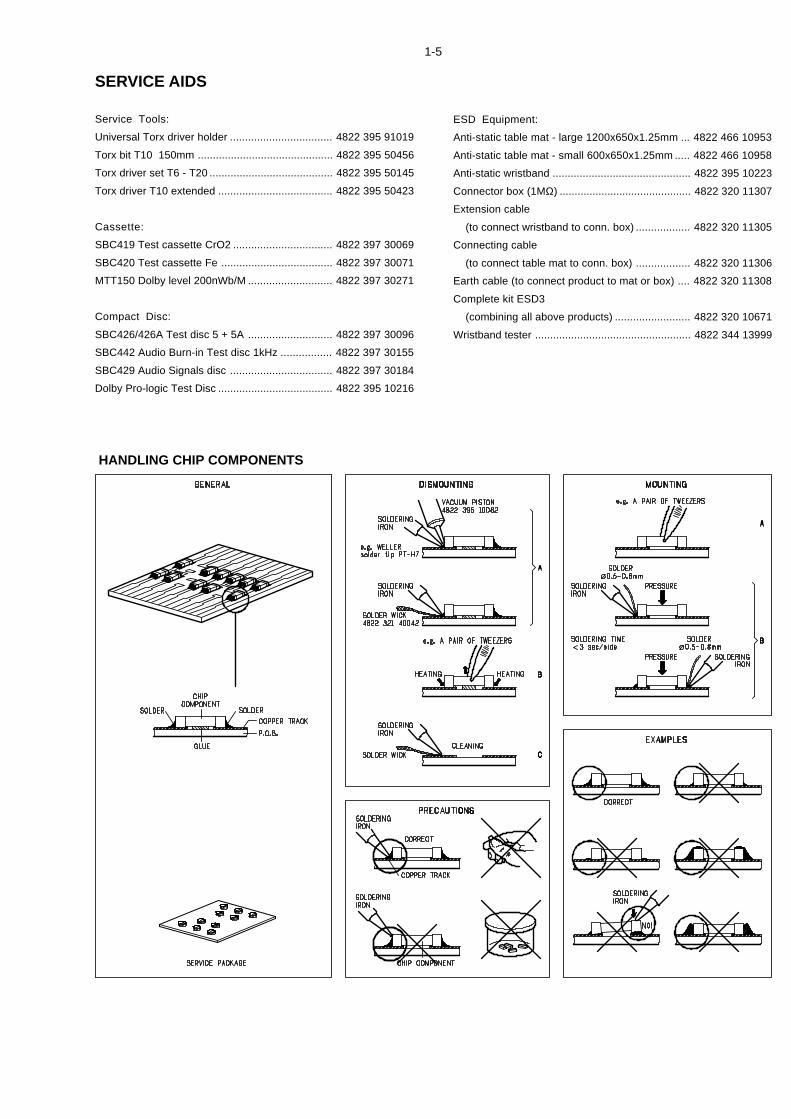
HANDLING CHIP COMPONENTS

1-6
GB WARNING
All ICs and many other semi-conductors aresusceptible to electrostatic discharges (ESD).Careless handling during repair can reduce lifedrastically.When repairing, make sure that you areconnected with the same potential as the massof the set via a wrist wrap with resistance.Keep components and tools also at thispotential.
F ATTENTION
Tous les IC et beaucoup d’autressemi-conducteurs sont sensibles auxdécharges statiques (ESD).Leur longévité pourrait être considérablementécourtée par le fait qu’aucune précaution n’estprise à leur manipulation.Lors de réparations, s’assurer de bien être reliéau même potentiel que la masse de l’appareil etenfiler le bracelet serti d’une résistance desécurité.Veiller à ce que les composants ainsi que lesoutils que l’on utilise soient également à cepotentiel.
ESD
D WARNUNG
Alle ICs und viele andere Halbleiter sindempfindlich gegenüber elektrostatischenEntladungen (ESD).Unsorgfältige Behandlung im Reparaturfall kandie Lebensdauer drastisch reduzieren.Veranlassen Sie, dass Sie im Reparaturfall überein Pulsarmband mit Widerstand verbundensind mit dem gleichen Potential wie die Massedes Gerätes.Bauteile und Hilfsmittel auch auf dieses gleichePotential halten.
NL WAARSCHUWING
Alle IC’s en vele andere halfgeleiders zijngevoelig voor electrostatische ontladingen(ESD).Onzorgvuldig behandelen tijdens reparatie kande levensduur drastisch doen verminderen.Zorg ervoor dat u tijdens reparatie via eenpolsband met weerstand verbonden bent methetzelfde potentiaal als de massa van hetapparaat.Houd componenten en hulpmiddelen ook opditzelfde potentiaal.
I AVVERTIMENTO
Tutti IC e parecchi semi-conduttori sonosensibili alle scariche statiche (ESD).La loro longevità potrebbe essere fortementeridatta in caso di non osservazione della piùgrande cauzione alla loro manipolazione.Durante le riparazioni occorre quindi esserecollegato allo stesso potenziale che quello dellamassa dell’apparecchio tramite un braccialettoa resistenza.Assicurarsi che i componenti e anche gli utensilicon quali si lavora siano anche a questopotenziale.
“Pour votre sécurité, ces documentsdoivent être utilisés par des spécia-listes agréés, seuls habilités à réparervotre appareil en panne”.
GBSafety regulations require that the set be restored to its originalcondition and that parts which are identical with those specified,be used.
NL
Veiligheidsbepalingen vereisen, dat het apparaat bij reparatie inzijn oorspronkelijke toestand wordt teruggebracht en dat onderdelen,identiek aan de gespecificeerde, worden toegepast.
F
Les normes de sécurité exigent que l’appareil soit remis à l’étatd’origine et que soient utiliséés les piéces de rechange identiquesà celles spécifiées.
D
Bei jeder Reparatur sind die geltenden Sicherheitsvorschriften zubeachten. Der Original zustand des Geräts darf nicht verändert werden;für Reparaturen sind Original-Ersatzteile zu verwenden.
I
Le norme di sicurezza esigono che l’apparecchio venga rimessonelle condizioni originali e che siano utilizzati i pezzi di ricambioidentici a quelli specificati.
"After servicing and before returning set to customer perform aleakage current measurement test from all exposed metal parts toearth ground to assure no shock hazard exist. The leakage currentmust not exceed 0.5mA."
CLASS 1LASER PRODUCT
3122 110 03420
GB Warning !Invisible laser radiation when open.Avoid direct exposure to beam.
S Varning !
Osynlig laserstrålning när apparaten är öppnad och spärrenär urkopplad. Betrakta ej strålen.
SF Varoitus !
Avatussa laitteessa ja suojalukituksen ohitettaessa olet alttiinanäkymättömälle laserisäteilylle. Älä katso säteeseen!
DK Advarse !
Usynlig laserstråling ved åbning når sikkerhedsafbrydere erude af funktion. Undgå udsaettelse for stråling.
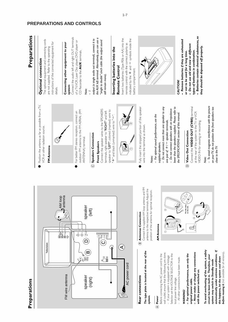
PREPARATIONS AND CONTROLS
1-7
Pre
par
atio
ns
Rea
r co
nn
ecti
on
s
The
typ
e p
late
is lo
cate
d at
the
rea
r of
the
syst
em.
AP
ower
Befo
re c
onne
ctin
g th
e A
C p
ower
cor
d to
the
wal
l out
let,
ensu
re t
hat
the
follo
win
g ar
e do
ne;
–If
your
sys
tem
is e
quip
ped
with
a V
olta
geSe
lect
or, s
et t
he V
OLT
AG
E SE
LEC
TOR
to
the
loca
l pow
er li
ne v
olta
ge.
–A
ll ot
her
conn
ectio
ns h
ave
been
mad
e.
WA
RN
ING
!–
For
opti
mal
per
form
ance
, use
onl
y th
eor
igin
al p
ower
cab
le.
–N
ever
mak
e or
cha
nge
any
conn
ecti
ons
wit
h th
e p
ower
sw
itch
ed o
n.
To a
void
ove
rhea
ting
of
the
syst
em, a
saf
ety
circ
uit
has
been
bui
lt in
. The
refo
re, y
our
syst
em m
ay s
wit
ch t
o St
andb
y m
ode
auto
mat
ical
ly u
nder
ext
rem
e co
ndit
ions
. If
this
hap
pen
s, le
t th
e sy
stem
coo
l dow
nbe
fore
reu
sing
it (
not a
vaila
ble
for a
ll ve
rsio
ns) .
BA
nte
nn
as C
on
nec
tio
nC
onne
ct t
he s
uppl
ied
AM
loop
ant
enna
and
FM
ante
nna
to t
he r
espe
ctiv
e te
rmin
als.
Adj
ust
the
posit
ion
of t
he a
nten
na fo
r op
timal
rec
eptio
n.
AM
An
ten
na
spea
ker
(rig
ht)
spea
ker
(left)
AC
pow
er c
ord
AM
loop
an
tenn
aF
M w
ire a
nten
na
A
BD C
VID
EO
IN
Tel
evis
ion
L
R
AU
DIO
O
UT
Pre
par
atio
ns
Po
sitio
n th
e an
tenn
a as
far
as p
ossib
le fr
om a
TV,
VC
R o
r ot
her
radi
atio
n so
urce
.
FM
An
ten
na
Fo
r be
tter
FM
ste
reo
rece
ptio
n, c
onne
ct a
nou
tdoo
r FM
ant
enna
to
the
FM A
ERIA
L (F
MA
NT
ENN
A)
term
inal
.
CS
pea
kers
Co
nn
ecti
on
Fro
nt
Sp
eake
rsC
onne
ct t
he s
peak
er w
ires
to t
he S
PEA
KER
Ste
rmin
als,
right
spe
aker
to
"RIG
HT
" and
left
spea
ker
to "L
EFT
", co
lore
d (m
arke
d) w
ire t
o"+
" and
bla
ck (
unm
arke
d) w
ire t
o "-
".
Fu
lly in
sert
the
str
ippe
d po
rtio
n of
the
spe
aker
wire
into
the
ter
min
al a
s sh
own.
Not
es:
–F o
r op
timal
sou
nd p
erfo
rman
ce, u
se th
esu
pplie
d sp
eake
rs.
–D
o no
t con
nect
mor
e th
an o
ne s
peak
er to
any
one
pair
of +
/- s
peak
er te
rmin
als.
–D
o no
t con
nect
spe
aker
s w
ith a
n im
peda
nce
low
er th
an th
e sp
eake
rs s
uppl
ied.
Ple
ase
refe
r to
the
SPEC
IFIC
ATIO
NS
sect
ion
of th
is m
anua
l.
D V
ideo
Ou
t C
on
nec
tio
n
Con
nect
the
VID
EO
OU
T (
CV
BS
) te
rmin
alat
the
rea
r of
the
sys
tem
to
the
TV
or V
CR
VID
EO IN
for
view
ing
or r
ecor
ding
.
Not
e:–
To a
void
mag
netic
inte
rfer
ence
with
the
pict
ure
on y
our T
V, do
not
pos
ition
the
front
spe
aker
s to
ocl
ose
to th
e TV
.
Op
tio
nal
co
nn
ecti
on
The
opt
iona
l equ
ipm
ent
and
conn
ectin
g co
rds
are
not
supp
lied.
Ref
er t
o th
e op
erat
ing
inst
ruct
ions
of t
he c
onne
cted
equ
ipm
ent
for
deta
ils.
Co
nn
ecti
ng
oth
er e
qu
ipm
ent
to y
ou
rsy
stem
Con
nect
the
aud
io le
ft an
d rig
ht O
UT
ter
min
als
of a
TV,
VC
R, L
aser
Disc
pla
yer,
DV
D p
laye
r or
CD
Rec
orde
r to
the
AU
X te
rmin
als.
Not
e:–
Iou
tput
(a s
ingl
e au
dio
out t
erm
inal
), co
nnec
t it t
oth
e AU
X le
ft te
rmin
al. A
ltern
ative
ly, y
ou c
an u
se a
“sin
gle
to d
oubl
e” c
inch
cab
le (
the
outp
ut s
ound
still
rem
ain
mon
o).
Inse
rtin
g b
atte
ries
into
th
eR
emo
te C
on
tro
lIn
sert
tw
o ba
tter
ies
(Typ
e R
06 o
r AA
) in
to t
here
mot
e co
ntro
l with
the
cor
rect
pol
arity
as
indi
cate
d by
the
+ a
nd -
sym
bols
insid
e th
eba
tter
y co
mpa
rtm
ent.
CA
UT
ION
!–
Rem
ove
batt
erie
s if
the
y ar
e ex
haus
ted
or n
ot t
o be
use
d fo
r a
long
tim
e.–
Do
not
use
old
and
new
or
diff
eren
tty
pes
of
batt
erie
s in
com
bina
tion
.–
Bat
teri
es c
onta
in c
hem
ical
sub
stan
ces,
soth
ey s
houl
d be
dis
pos
ed o
ff p
rop
erly
.
PREPARATIONS AND CONTROLS
1-8
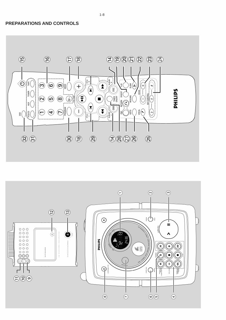
2 31
8 6 457
90!
@ #
⁄ º ª* §$ •
£™¡)($& *^%¤ ∞27
24
PREPARATIONS AND CONTROLS
1-9
Co
ntr
ols
Co
ntr
ols
on
th
e sy
stem
an
dre
mo
te c
on
tro
l
1D
isp
lay
–sh
ows
the
stat
us o
f the
sys
tem
.2
PR
OG
/ RE
Vfo
r VC
D/ C
D/ M
P3....
..pro
gram
mes
tra
cks
and
revi
ews
the
prog
ram
me.
for T
UN
ER....
........
........
....pr
ogra
mm
es t
uner
stat
ions
man
ually
or
auto
mat
ical
ly.fo
r TA
PE....
........
........
........
.. set
s ta
pe r
ever
se m
ode
3C
LO
CK
SE
T
for
CLO
CK
........
........
.......
set
the
cloc
k fu
nctio
n.fo
r VC
D/ C
D/ M
P3....
.. sta
rts
or in
terr
upts
CD
play
back
for T
APE
........
........
........
...... s
tart
s th
e ta
pe p
layb
ack
4M
od
e S
elec
tio
nV
OL
UM
E (-
/+)
–ad
just
s th
e vo
lum
e le
vel.
–on
the
syst
em o
nly
- ad
just
s th
e ho
ur a
nd m
inut
esfo
r th
e cl
ock/
timer
func
tions
.P
RE
SE
T/
TIM
ER
SE
T
/ (
TIT
LE
–/+
)fo
r TU
NER
........
........
........
sele
cts
a pr
eset
rad
iost
atio
n.fo
r VC
D/ C
D/ M
P3....
.. ski
ps t
o th
e be
ginn
ing
of a
curr
ent
trac
k/ p
revi
ous/
subs
eque
nt t
rack
........
........
........
........
........
........
.sel
ect
next
or
prev
ious
men
ufo
r Tim
er (
onl
y) t
o se
t tim
er u
nder
sta
ndby
SE
AR
CH
/ TU
NE
/
(A
LB
UM
–/+
)fo
r TU
NER
........
........
........
Tune
to
a st
atio
nfo
r VC
D/ C
D....
........
.......
fast
sea
rche
s ba
ck a
ndfo
rwar
d w
ithin
a t
rack
.fo
r M
P3....
........
........
........
...A
LBU
M s
elec
t.fo
r TA
PE....
........
........
........
.. fas
t re
win
d/ w
ind
tape
ST
OP
9
for V
CD
/ CD
/ MP3
...... s
tops
VC
D/ C
D/ M
P3pl
ayba
ck o
r er
ase
a VC
D/
CD
/ MP3
pro
gram
me.
for T
UN
ER....
........
........
....st
ops
prog
ram
min
gfo
r TA
PE....
........
........
........
..sto
ps t
ape
play
back
/re
cord
ing.
RE
C
........
........
........
.......
star
ts r
ecor
ding
.
5S
OU
RC
E
–se
lect
s th
e re
spec
ti ve
soun
d so
urce
for
CD
/T
UN
ER/ T
APE
/AU
X.
–sw
itche
s on
the
sys
tem
.6
DIS
PL
AY-
BA
ND
for T
UN
ER....
........
........
....ch
ange
the
tun
er r
adio
band
.(FM
/ MW
)fo
r VC
D/ C
D/ M
P3....
..cha
nge
the
CD
disp
l ay
mod
efo
r TA
PE....
........
........
........
.. sel
ect
tape
dire
ctio
n7
iR S
EN
SO
R–
infr
ared
sen
sor
for
rem
ote
cont
rol.
8S
TA
ND
BY
ON
2–
switc
hes
the
syst
em t
o st
andb
y.9
PH
ON
ES
- co
nnec
ts t
o he
adph
one.
0L
EV
EL
(m
ic)
–to
adj
ust
the
mix
ing
leve
l for
kar
aoke
or
mic
roph
one
reco
rdin
g.
!M
IC–
to c
onne
ct m
icro
phon
e ja
ck.
@ –op
en/ c
lose
the
cas
sett
e do
or.
#C
D O
PE
N
–op
en t
he C
D d
oor.
$IN
TE
RA
CT
IVE
SO
UN
D c
on
tro
ls:
DB
B....
........
........
........
........
(Dyn
amic
Bas
s Bo
ost)
enha
nces
the
bas
s.D
SC
........
........
........
........
..... (
Dig
ital S
ound
Con
trol
)se
lect
s so
und
char
acte
ristic
s: C
LASS
IC/
JAZ
Z/ R
OC
K/ O
PTIM
AL.
%2
–to
sw
itch
the
syst
em t
o St
andb
y m
ode.
^D
IGIT
0/-
- –
9(n
umbe
rs c
onsis
ting
mor
e th
an tw
o or
thre
e fig
ures
mus
t be
Pres
s &
hol
d 0/
--.)
–to
sel
ect
a tr
ack
num
ber
for
CD
/VC
D/M
P3-C
D.
–to
sel
ect
tune
r pr
eset
.&
MO
DE
RE
PE
AT
–re
peat
s a
trac
k/ C
D p
rogr
amm
e/ e
ntire
CD
.S
HU
FF
LE
–pl
ays
CD
tra
cks
in r
ando
m o
rder
.
Co
ntr
ols
*V
OL
UM
E (-
/+)
–to
incr
ease
or
decr
ease
the
vol
ume .
–ad
just
s th
e ho
ur a
nd m
inut
es fo
r th
e cl
ock/
tim
esju
nctio
ns.
(D
IGE
ST
–to
sca
n th
roug
h a
VC
D o
r a
spec
ific
trac
k.)
A -
B–
to p
layb
ack
a ce
rtai
n sc
ene
or p
assa
ge o
f a C
D/
VC
D r
epea
tedl
y.¡
SLO
WÖ
–to
wat
ch t
he V
CD
at
a slo
wer
spe
ed.
™R
ES
UM
E–
to c
ontin
ue p
layb
ack
agai
n fr
om w
here
you
hav
est
oppe
d (f
or V
CD
with
PBC
sw
itche
d of
f).
£E
CH
O-
/+–
to a
djus
t th
e V
CD
ech
o le
vel f
or k
arao
ke a
fter
inse
rted
the
mic
roph
one.
KE
Y C
ON
TR
OL
(I È i
)–
to c
hang
e th
e V
CD
key
ton
e le
vel t
o su
it yo
urvo
cal r
ange
.I
........
........
........
...to
dec
reas
e th
e ke
y to
ne le
vel.
È....
........
........
........
.. to
rest
ore
the
key
tone
leve
l to
orig
inal
set
ting.
i....
........
........
........
. to
incr
ease
the
key
ton
e le
vel.
VO
CA
L–
to fa
de o
ut t
he o
rigin
al v
ocal
from
a K
arao
keV
CD
or
to s
witc
h be
twee
n m
ono
or s
tere
om
ode
durin
g au
dio
disc
pla
ybac
k.§
GO
TO
–se
lect
tim
e to
beg
in p
layb
ack
with
in t
rack
.V
CD
Op
erat
ion
(fo
r VCD
ver
sion
2.0
only)
PB
C (
PL
AY
BA
CK
CO
NT
RO
L)
–to
sw
itch
on o
r of
f PBC
mod
e.R
ET
UR
N–
to r
etur
n to
the
pre
viou
s M
ENU
leve
l dur
ing
play
back
(fo
r VC
D w
ith P
BC s
witc
hed
on).
•T
IME
R O
N /
OF
F–
activ
ates
/dea
ctiv
ates
the
tim
er fu
nctio
n.
ªM
od
e S
elec
tio
nP
LA
Y P
AU
SE
fo
r C
D/V
CD
/MP3
-CD
…to
sta
rt o
r in
terr
upt
play
back
.fo
r TA
PE....
........
........
........
........
to s
tart
pla
ybac
k.à
/ á
(AL
BU
M ---- -
/ ++++ +)
for
MP3
-CD
onl
y....
........
....to
sel
ect
prev
ious
/nex
tA
lbum
for
CD
/VC
D....
........
........
...... t
o se
arch
bac
kwar
d/fo
rwar
d.fo
r TU
NER
........
........
........
...... t
o tu
ne t
o a
low
er o
rhi
gher
rad
io fr
eque
ncy.
for T
APE
........
........
........
........
....to
rew
ind
or fa
stfo
rwar
d.S
TO
P Ç
for
CD
/VC
D/M
P3-C
D....
. to
stop
pla
ybac
k or
to
clea
r a
prog
ram
me.
for T
APE
........
........
........
........
....to
sto
p pl
ayba
ck o
rre
cord
ing.
........
........
........
........
........
........
.......
to r
eset
tap
e co
unte
rnu
mbe
r.í
/ ë
(TIT
LE---- -
/ ++++ +)
for
MP3
-CD
onl
y....
........
....to
sel
ect
prev
ious
/nex
tT
itle.
for V
CD
onl
y....
........
........
......t
o se
lect
nex
t or
prev
ious
MEN
U o
rV
CD
tra
ck d
urin
gpl
ayba
ck (
for V
CD w
ithPB
C sw
itche
d on
).fo
r C
D/V
CD
........
........
........
.. to
skip
to
the
prev
ious
or n
ext
trac
k.fo
r TU
NER
........
........
........
...... t
o se
lect
a p
rese
t ra
dio
stat
ion.
ºP
RO
GR
AM
for
CD
/VC
D/M
P3-C
D…
to
prog
ram
me
disc
trac
ks.
for T
UN
ER....
........
........
........
.. to
prog
ram
me
pres
etra
dio
stat
ions
man
ually
or a
utom
atic
ally
⁄V
CD
/ CD
24
25
27
1-10
Co
ntr
ols
Not
es f
or r
emot
e co
ntro
l:–
Firs
t, se
lect
the
sou
rce
you
wis
h to
con
trol
by p
ress
ing
one
of t
he s
ourc
e se
lect
key
s on
the
rem
ote
cont
rol (
VCD
/ CD
or T
UN
ER
, for
exam
ple)
.–
The
n se
lect
the
des
ired
fun
ctio
n (
, ,
fo
r ex
ampl
e).
–to
sel
ect
disc
(th
is sy
stem
can
pla
ybac
k no
rmal
CD
/VC
D/M
P3-C
D fo
rmat
disc
).–
to s
elec
t co
rres
pond
ing
vide
o ou
tput
for
NT
SCor
PA
L sy
stem
of y
our T
V s
et (
exce
pt M
ulti-
syst
em T
V).
TU
NE
R–
to s
elec
t tu
ners
mod
e.T
AP
E–
to s
elec
t ta
pe d
eck
mod
e.A
UX
/ (C
DR
/DV
D)
–to
sel
ect
a co
nnec
ted
exte
rnal
sou
rce
:C
DR
/DV
D o
r AU
X (
auxi
liary
) m
ode.
OS
D (
ON
SC
RE
EN
DIS
PL
AY
)–
to s
witc
h on
or
off t
he o
n sc
reen
disp
lay
on t
heT
V.
PREPARATIONS AND CONTROLS
TROUBLESHOOTING
Tro
ubl
esh
oo
tin
g
WA
RN
ING
Und
er n
o ci
rcum
stan
ces
shou
ld y
ou t
ry t
o re
pai
r th
e sy
stem
you
rsel
f, as
thi
s w
ill in
valid
ate
the
war
rant
y. D
o no
t op
en t
he s
yste
m a
s th
ere
is a
ris
k of
ele
ctri
c sh
ock.
If a
fau
lt o
ccur
s, fi
rst
chec
k th
e p
oint
s lis
ted
belo
w b
efor
e ta
king
the
sys
tem
for
rep
air.
If y
ouar
e un
able
to
rem
edy
a p
robl
em b
y fo
llow
ing
thes
e hi
nts,
con
sult
you
r de
aler
or
serv
ice
cent
er.
Pro
blem
So
luti
on
CD
OP
ER
AT
ION
“NO DISC
” is
dis
pla
yed
.–
Inse
rt a
disc
.–
Che
ck if
the
disc
is in
sert
ed u
psid
e do
wn.
–W
ait
until
the
moi
stur
e co
nden
satio
n at
the
lens
has
clea
red.
–R
epla
ce o
r cl
ean
the
disc
, see
“M
aint
enan
ce”.
–U
se a
fina
lised
CD
-RW
or
CD
-R.
No
pic
ture
on
TV
scr
een
.–
Con
nect
the
cab
le b
etw
en t
he s
yste
m a
nd T
V.
No
co
lou
r o
n T
V.
–C
hang
e th
e sy
stem
to
the
resp
ectiv
e PA
L or
NT
SC s
ettin
g.
Can
no
t ad
just
th
e T
V s
yste
m t
o–
Rem
ove
the
MP-
3 C
D fr
om d
isc t
r ay
PAL
or
NT
SC
.
Mai
nte
nan
ce
Cle
anin
g th
e C
abin
et
Use
a s
oft
clot
h sli
ghtly
moi
sten
ed w
ith a
mild
dete
rgen
t so
lutio
n. D
o no
t us
e a
solu
tion
cont
aini
ng a
lcoh
ol, s
pirit
s, am
mon
ia o
r ab
rasiv
es.
Cle
anin
g D
iscs
W
hen
a di
sc b
ecom
es d
irty
,cl
ean
it w
ith a
cle
anin
g cl
oth.
Wip
e th
e di
sc fr
om t
he c
entr
eou
t.
Do
not
use
solv
ents
suc
h as
benz
ene,
thi
nner
, com
mer
cial
lyav
aila
ble
clea
ners
, or
antis
tatic
spra
y in
tend
ed fo
r an
alog
ue r
ecor
ds.
Cle
anin
g th
e d
isc
len
s
Afte
r pr
olon
ged
use,
dir
t or
dus
t m
ayac
cum
ulat
e at
the
disc
lens
. To
ensu
re g
ood
play
back
qua
lity,
clea
n th
e di
sc le
ns w
ith P
hilip
sC
D L
ens
Cle
aner
or
any
com
mer
cial
ly a
vaila
ble
clea
ner.
Follo
w t
he in
stru
ctio
ns s
uppl
ied
with
clea
ner.
Cle
anin
g th
e H
ead
s an
d t
he
Tap
e P
ath
s
To e
nsur
e go
od r
ecor
ding
and
pla
ybac
k qu
ality
,cl
ean
the
head
s A
, the
cap
stan
(s) B
, and
pres
sure
rol
ler(
s) C
afte
r ev
ery
50 h
ours
of
tape
ope
ratio
n.C
auti
on: D
o no
t ro
tate
the
hea
ds d
urin
gcl
eani
ng.
U
se a
cot
ton
swab
slig
htly
moi
sten
ed w
ithcl
eani
ng fl
uid
or a
lcoh
ol.
Yo
u ca
n al
so c
lean
the
hea
ds b
y pl
ayin
g a
clea
ning
tap
e on
ce.
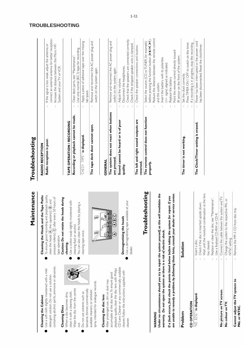
AA
BC
Dem
agn
etis
ing
the
hea
ds
U
se a
dem
agne
tisin
g ta
pe a
vaila
ble
at y
our
deal
er.
Tro
ubl
esh
oo
tin
g
RA
DIO
RE
CE
PT
ION
Rad
io r
ecep
tio
n is
po
or.
–If
the
signa
l is
too
wea
k, ad
just
the
ant
enna
or
conn
ect
an e
xter
nal a
nten
na fo
r be
tter
rec
eptio
n.–
Incr
ease
the
dist
ance
bet
wee
n th
e M
icro
HiF
iSy
stem
and
you
r TV
or V
CR
.
TA
PE
OP
ER
AT
ION
/ R
EC
OR
DIN
G
Rec
ord
ing
or
pla
ybac
k ca
nn
ot
be
mad
e.–
Cle
an d
eck
part
s, se
e “M
aint
enan
ce”.
–U
se o
nly
norm
al (
IEC
I) t
ape
for
reco
rdin
g.
“CHECK TAPE
” is
dis
pla
yed
.–
App
ly a
pie
ce o
f adh
esiv
e ta
pe o
ver
the
miss
ing
tab
spac
e.
Th
e ta
pe
dec
k d
oo
r ca
nn
ot
op
en.
–R
emov
e an
d re
conn
ect
the
AC
pow
er p
lug
and
switc
h on
the
sys
tem
aga
in.
GE
NE
RA
L
Th
e sy
stem
do
es n
ot
r eac
t w
hen
bu
tto
ns
–R
emov
e an
d re
conn
ect
the
AC
pow
er p
lug
and
are
pre
ssed
.sw
itch
on t
he s
yste
m a
gain
.
So
un
d c
ann
ot
be
hea
rd o
r is
of
po
or
–A
djus
t th
e vo
lum
e.q
ual
ity.
–D
iscon
nect
the
hea
dpho
nes.
–C
heck
tha
t th
e sp
eake
rs a
re c
onne
cted
cor
rect
ly.–
Che
ck if
the
str
ippe
d sp
eake
r w
ire is
cla
mpe
d.
Th
e le
ft a
nd
rig
ht
sou
nd
ou
tpu
ts a
re–
Che
ck t
he s
peak
er c
onne
ctio
ns a
nd lo
catio
n.re
vers
ed.
Th
e re
mo
te c
on
tro
l do
es n
ot
fun
ctio
n–
Sele
ct t
he s
ourc
e (C
D o
r TU
NER
, for
exa
mpl
e)p
rop
erly
.be
fore
pre
ssin
g th
e fu
nctio
n bu
tton
(,
, )
.–
Red
uce
the
dist
ance
bet
wee
n th
e re
mot
e co
ntro
lan
d th
e sy
stem
.–
Inse
rt t
he b
atte
ry w
ith it
s po
larit
ies
(+/–
sig
ns)
alig
ned
as in
dica
ted.
–R
epla
ce t
he b
atte
ry.
–Po
int
the
rem
ote
cont
rol d
irect
ly t
owar
dIR
sen
sor
on t
he fr
ont
of t
he s
yste
m.
Th
e ti
mer
is n
ot
wo
rkin
g.–
Set
the
cloc
k co
rrec
tly.
–Pr
ess T
IMER
ON
/ O
FF t
o sw
itch
on t
he t
imer
.–
If a
reco
rdin
g is
in p
rogr
ess,
stop
the
rec
ordi
ng.
Th
e C
lock
/Tim
er s
etti
ng
is e
rase
d.
–Po
wer
has
bee
n in
terr
upte
d or
the
pow
er c
ord
has
been
disc
onne
cted
. Res
et t
he c
lock
/tim
er.
1-11

1-12
TROUBLESHOOTING
2-1 2-1
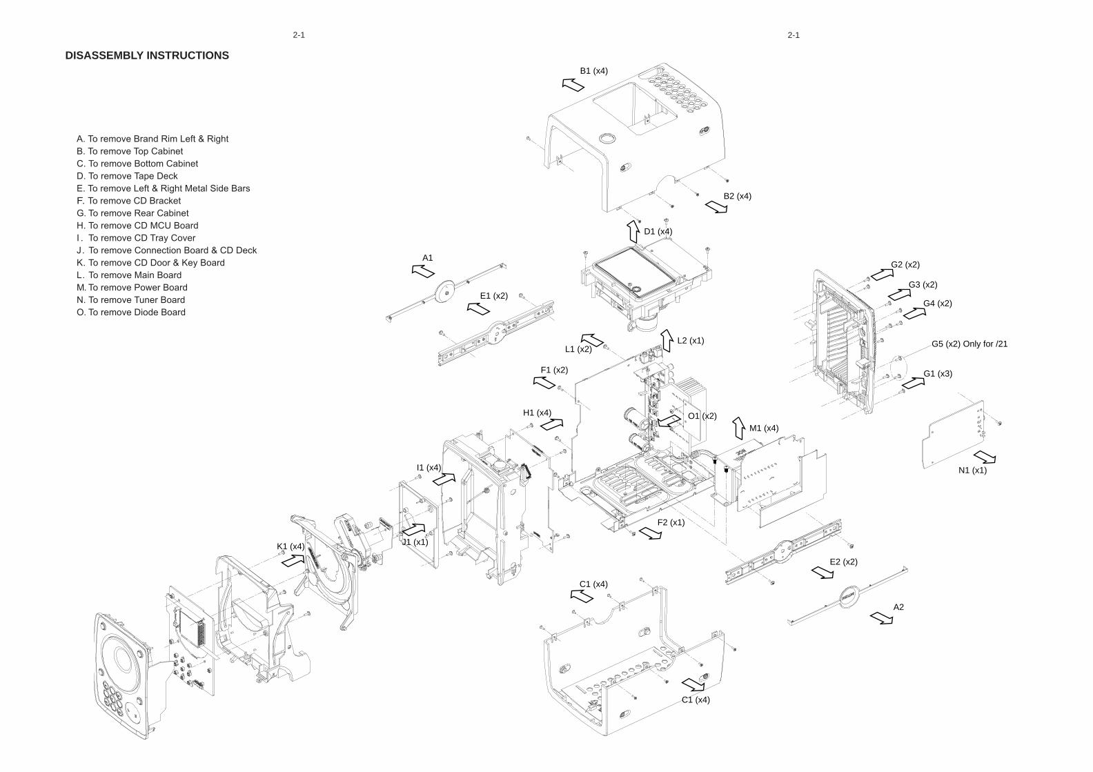
DISASSEMBLY INSTRUCTIONS
A. To remove Brand Rim Left & Right
B. To remove Top Cabinet
C. To remove Bottom Cabinet
D. To remove Tape Deck
E. To remove Left & Right Metal Side Bars
F. To remove CD Bracket
G. To remove Rear Cabinet
H. To remove CD MCU Board
I . To remove CD Tray Cover
J. To remove Connection Board & CD Deck
K. To remove CD Door & Key Board
L. To remove Main Board
M. To remove Power Board
N. To remove Tuner Board
O. To remove Diode Board
A2
E2 (x2)
B2 (x4)
B1 (x4)
D1 (x4)
E1 (x2)
A1
F1 (x2)
F2 (x1)
C1 (x4)
C1 (x4)
G5 (x2) Only for /21
G1 (x3)
G2 (x2)
G3 (x2)
G4 (x2)
L1 (x2)L2 (x1)
H1 (x4)
I1 (x4)
K1 (x4)
M1 (x4)
N1 (x1)
J1 (x1)
O1 (x2)

2-2 2-2

3-1 3-1
SET BLOCK DIAGRAM
L
TO POWER
R SUPPLY
TO CASS DECK
PRE-AMP
NJM4556AM
VC
C S
W
D60
2
D60
3
VL:8
V
VH:1
6V
+ CD 8V
+12V KA7812
CD-LCD-R
TDA T468DFUNCTION IC
POWERAMP
AN17830ASPK
HEADPHONE OUT
MCUTMP87EP26F
AMRF
AM IF
IC 101TA2149BN
FMIF
PLLTC
9257F
FMOSC
FM RF
TA 8142AP
P/B-R
85KHZ
+6V L7806REC-R
BA316NCASSETTDECK
OSC
DSPTC9462F
RFTA2153FN
DRIVE ICTA2092N
CDDECK
POWERSUPPLY
AM OSC
AUX
TU-R
AM ANT
TU-L
P/B-L
REC-L
LCD DRIVE ICHT1622
LCD
STP16N106
VIDEOES3207FP
MPEGES3210FP
DRAM256Kx16
EPROM27C020
VOLTAGEREGULATOR
NTCRES FAN

4-1 4-1
SET WIRING DIAGRAM
5-1
KEY BOARD
TABLE OF CONTENTS
IC Block Diagram........................................................................ 8-1
Circuit Diagram ........................................................................... 8-2
Layout Diagram-Component ...................................................... 8-3
Layout Diagram-SMD ................................................................. 8-3
Electrical parts list ...................................................................... 8-4
5-1
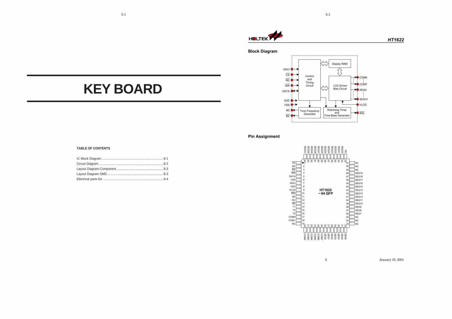
Block Diagram
Pin Assignment
HT1622
2 January 10, 2001
! " # $ % & ' ( ) !
% & ' $ * ' $ ' ) ' ( " (
% * + , - $
$ ( % . ' ( / % * $ % ( 0 %
" ) ( " ,
) !
% & % ) #
% ( 0 %
" ) ' $ 1 ( ' 2 0 ' ) - ' ) ' ( " (
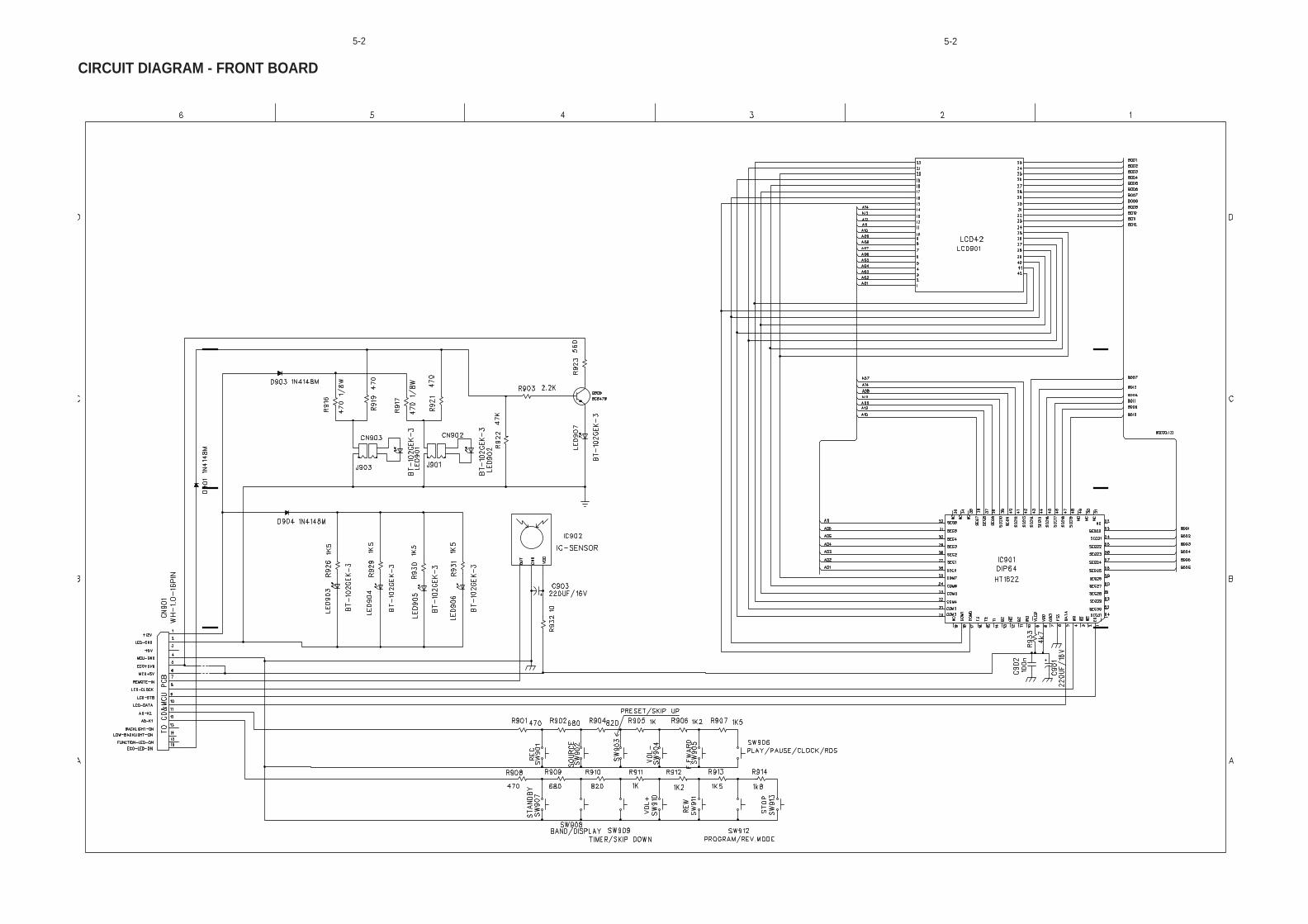
CIRCUIT DIAGRAM - FRONT BOARD
5-2 5-2
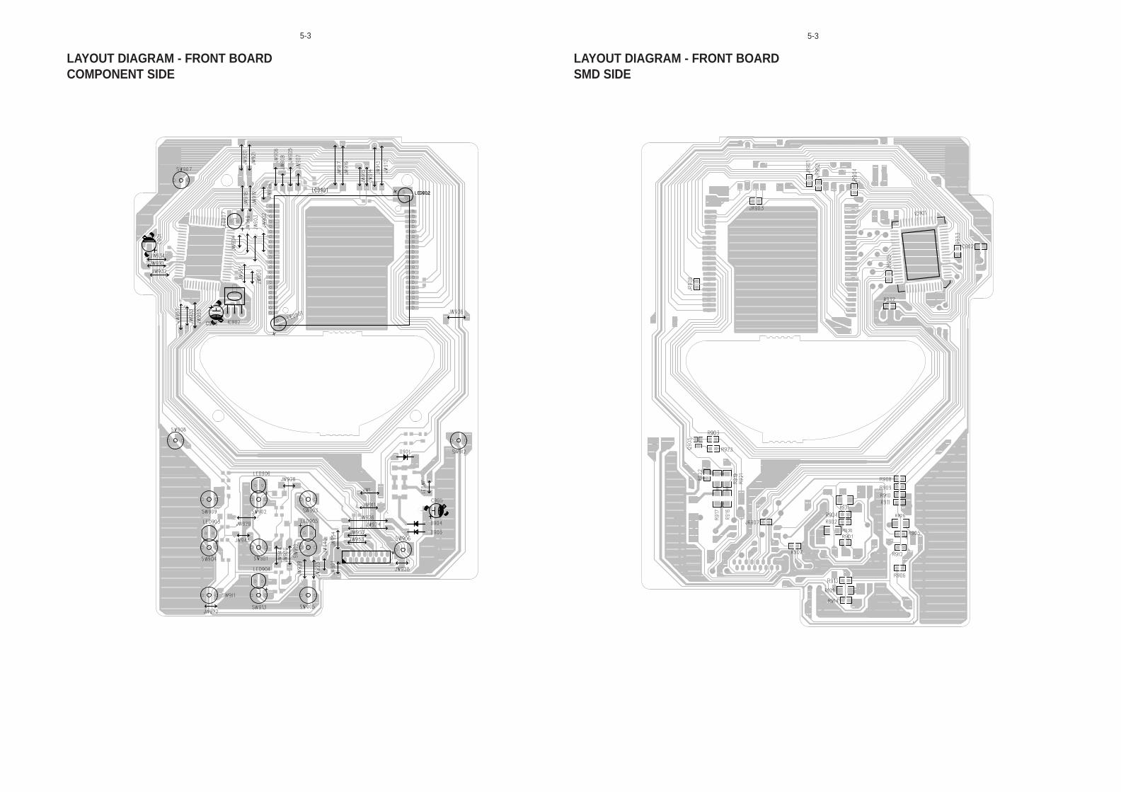
LAYOUT DIAGRAM - FRONT BOARDCOMPONENT SIDE
5-3 5-3
LAYOUT DIAGRAM - FRONT BOARDSMD SIDE
5-4 5-4
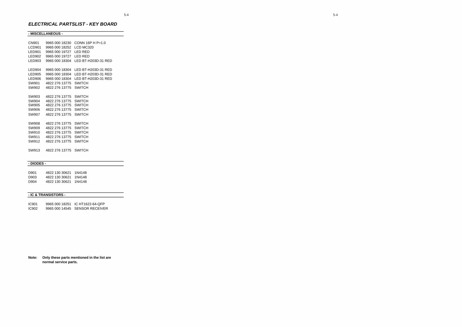
ELECTRICAL PARTSLIST - KEY BOARD
- MISCELLANEOUS -
CN901 9965 000 18230 CONN 16P H P=1.0LCD901 9965 000 18252 LCD MC320LED901 9965 000 19727 LED REDLED902 9965 000 19727 LED REDLED903 9965 000 18304 LED BT-H203D-31 RED
LED904 9965 000 18304 LED BT-H203D-31 REDLED905 9965 000 18304 LED BT-H203D-31 REDLED906 9965 000 18304 LED BT-H203D-31 REDSW901 4822 276 13775 SWITCHSW902 4822 276 13775 SWITCH
SW903 4822 276 13775 SWITCHSW904 4822 276 13775 SWITCHSW905 4822 276 13775 SWITCHSW906 4822 276 13775 SWITCHSW907 4822 276 13775 SWITCH
SW908 4822 276 13775 SWITCHSW909 4822 276 13775 SWITCHSW910 4822 276 13775 SWITCHSW911 4822 276 13775 SWITCHSW912 4822 276 13775 SWITCH
SW913 4822 276 13775 SWITCH
- DIODES -
D901 4822 130 30621 1N4148D903 4822 130 30621 1N4148D904 4822 130 30621 1N4148
- IC & TRANSISTORS -
IC901 9965 000 18251 IC HT1622-64-QFPIC902 9965 000 14545 SENSOR RECEIVER
Note: Only these parts mentioned in the list are normal service parts.
POWER BOARD
TABLE OF CONTENTS
CircuitDiagram ..............................................................6-2
PCB Layout ....................................................................6-3
Electrical PartsList..........................................................6-4
6-1 6-1
6-2 6-2
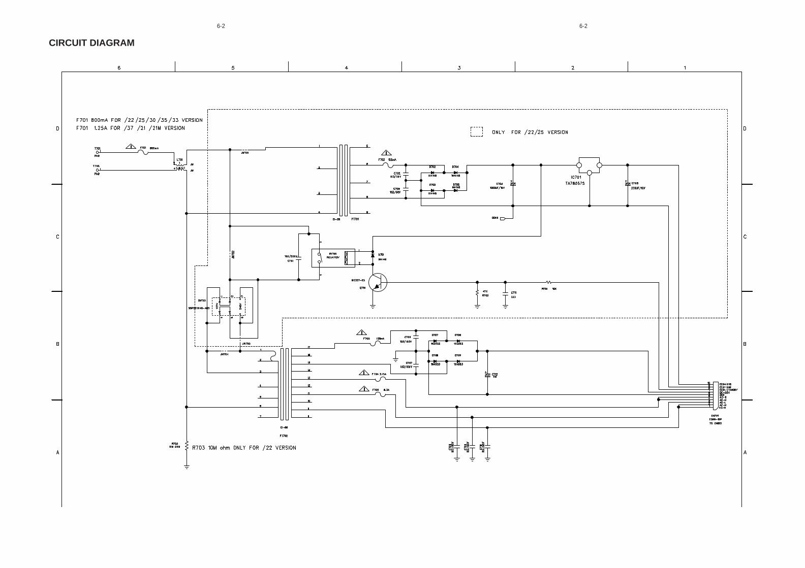
CIRCUIT DIAGRAM
6-3 6-3
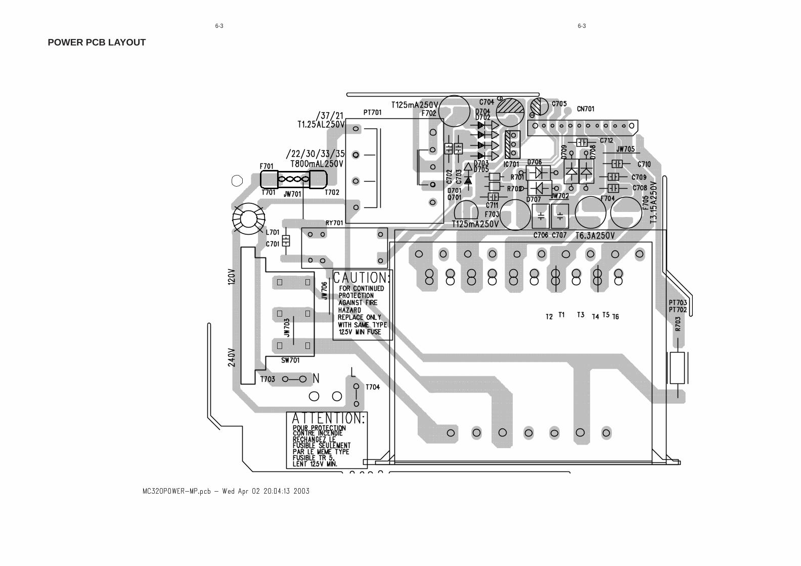
POWER PCB LAYOUT

6-4 6-4
ELECTRICAL PARTSLIST - POWER BOARD
- MISCELLANEOUS -
CN701 9965 000 19724 CON BM V 10P M 2.5 EHBF701 9965 000 19725 FUSE 1.6A TSD1.6A 250V /21F703 9965 000 18246 FUSE 125MA TAPPINGF704 9965 000 18247 FUSE 6.3A TAPPINGF705 9965 000 18248 FUSE 3.15A TAPPING
PT702 9965 000 18219 POWER TRANS. EI-66 H /21SW701 9965 000 11348 VOLTAGE SELECTOR 2P 5AT703 9965 000 18250 CONNECTORT704 9965 000 18250 CONNECTOR
- COILS & FILTERS -
L701 9965 000 11379 FILTER MAINS 400µH
- DIODES -
D706 4822 130 31878 1N4003GD707 4822 130 31878 1N4003GD708 4822 130 31878 1N4003GD709 4822 130 31878 1N4003G
Note: Only these parts mentioned in the list are normal service parts.
!
!
!
!
!
!
7-1
TUNER BOARD
TABLE OF CONTENTS
IC Block Diagram............................................................. 7-2 to 7-7
Circuit Diagram_Non Cenelec .................................................... 7-8
Layout Diagram-Component_Non Cenelec ............................... 7-9
Layout Diagram-SMD_Non Cenelec .......................................... 7-9
Electrical parts list .................................................................... 7-10
7-1
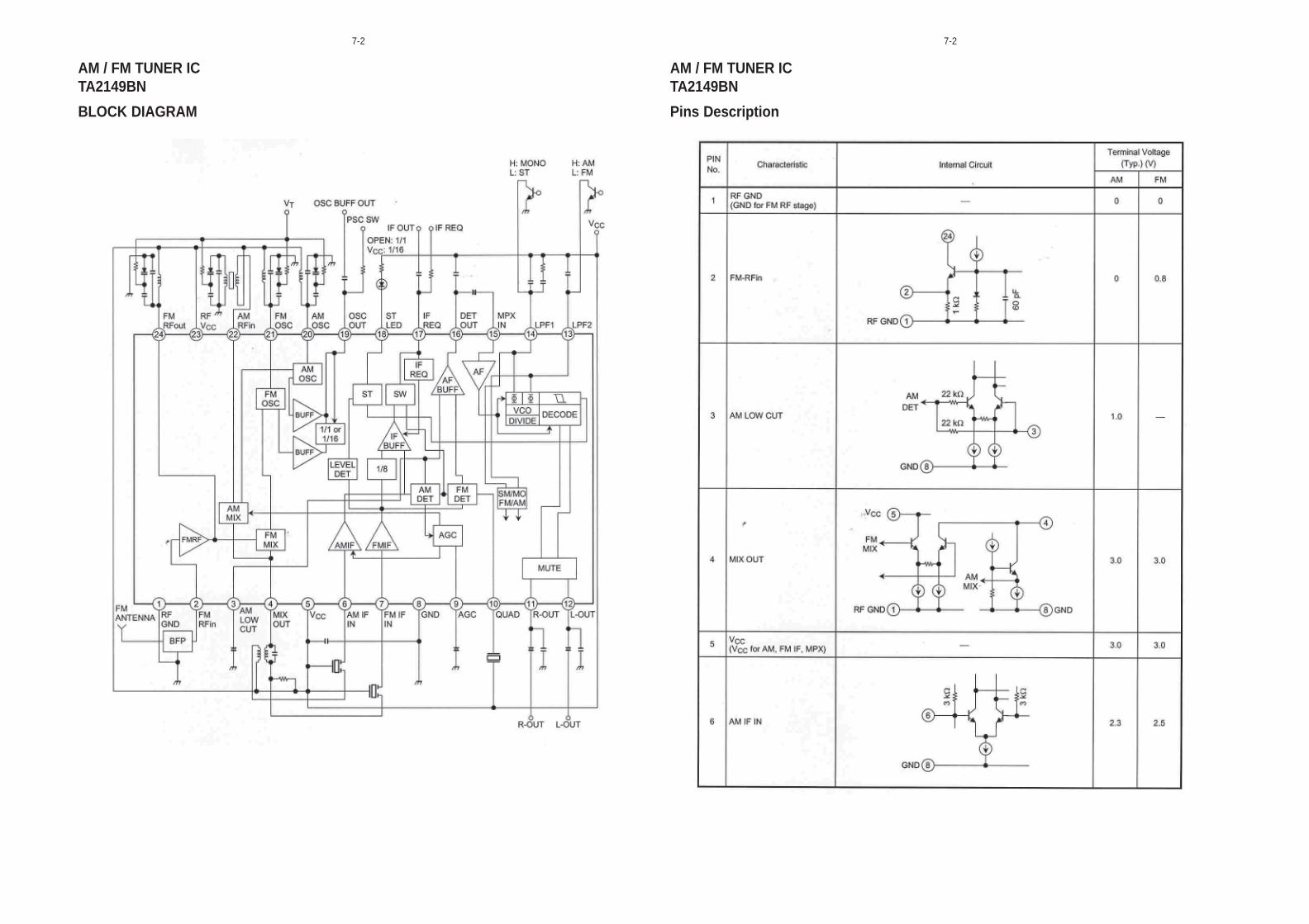
AM / FM TUNER ICTA2149BN
AM / FM TUNER ICTA2149BN
BLOCK DIAGRAM Pins Description
7-2 7-2
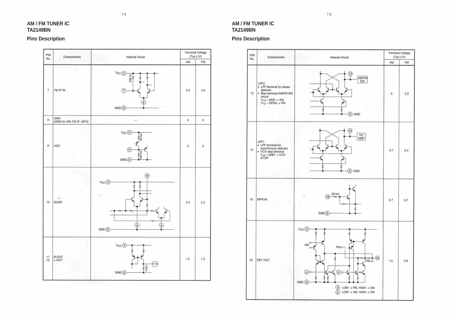
AM / FM TUNER ICTA2149BN
Pins Description Pins Description
AM / FM TUNER ICTA2149BN
7-3 7-3
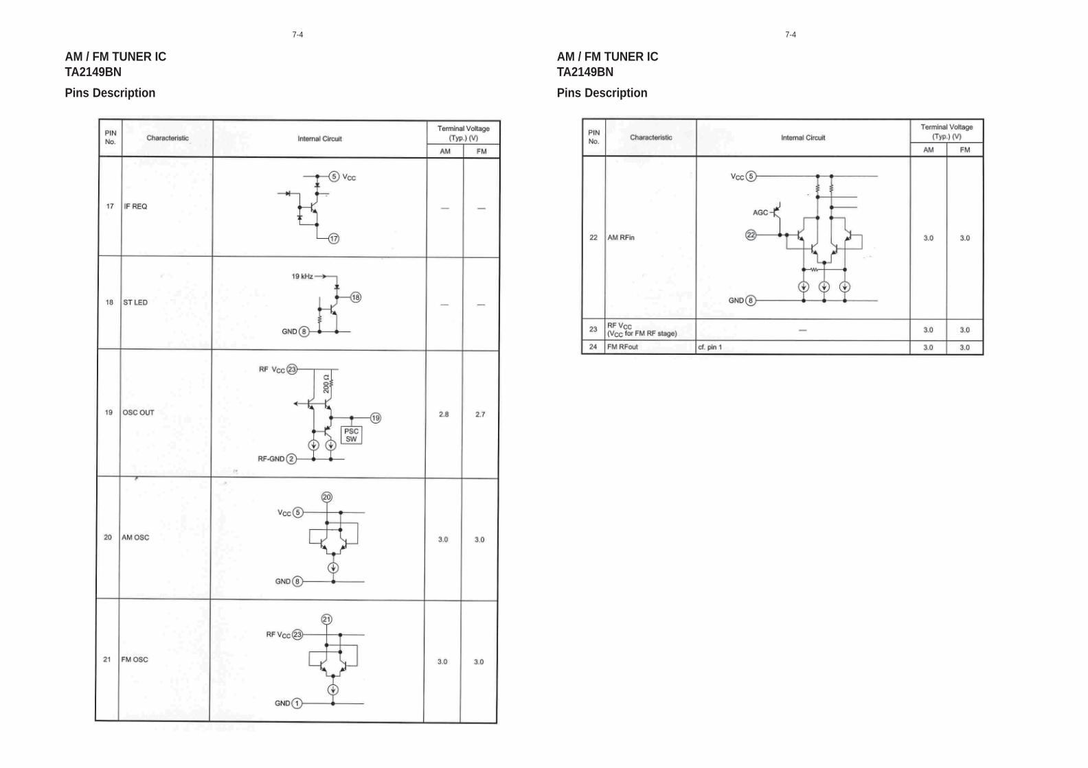
AM / FM TUNER ICTA2149BN
Pins Description
AM / FM TUNER ICTA2149BN
Pins Description
7-4 7-4
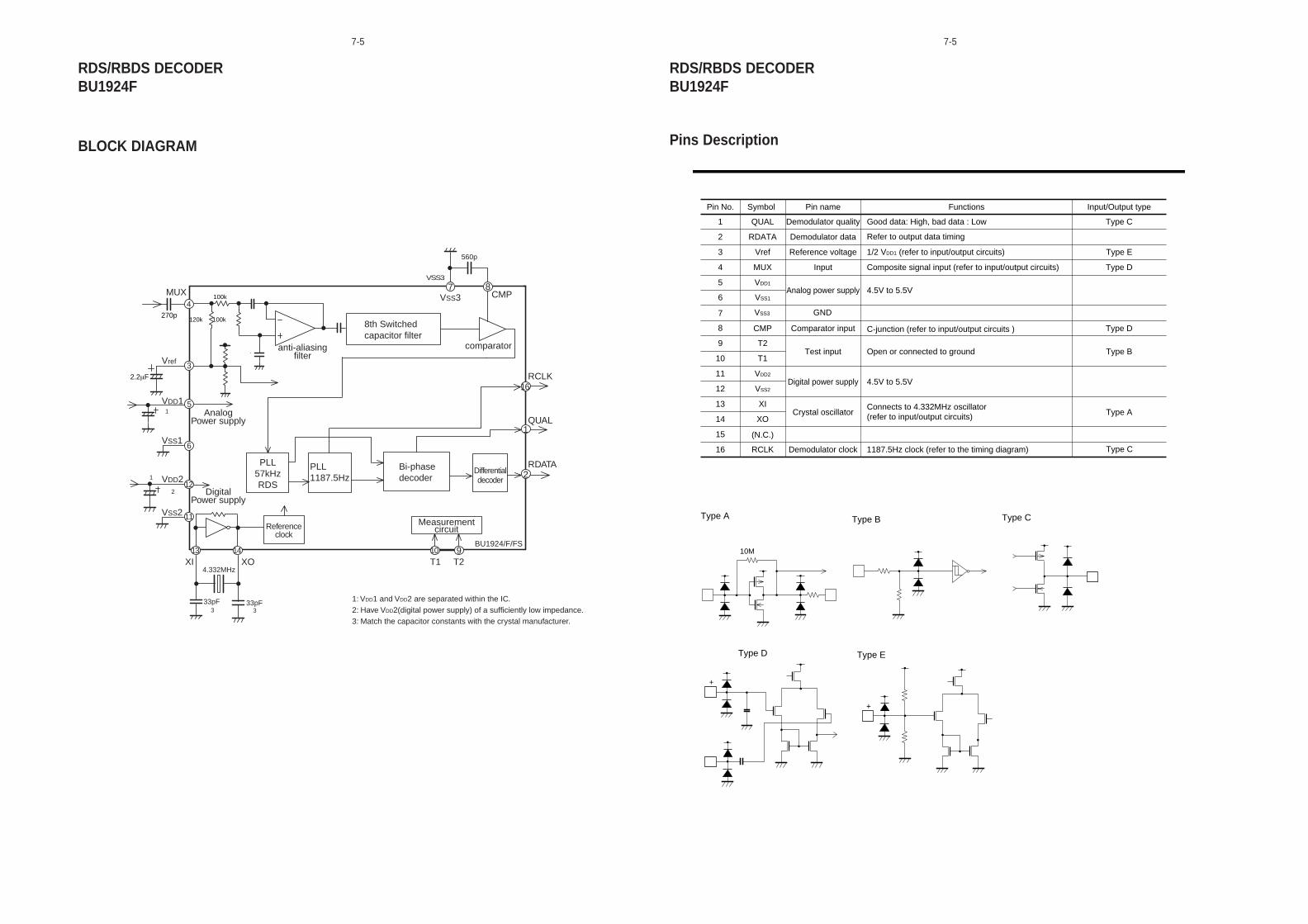
Pin No. Pin nameSymbol Functions Input/Output type
1 QUAL Demodulator quality Type CGood data: High, bad data : Low
Refer to output data timing
6 VSS1
7
CMP Comparator input Type DC-junction (refer to input/output circuits )8
VSS3 GND
2 RDATA Demodulator data
9 T2Test input Type BOpen or connected to ground
10 T1
3 Vref Reference voltage
4 MUX Input
Type E
Type D
1/2 VDD1 (refer to input/output circuits)
Composite signal input (refer to input/output circuits)
11 VDD2
Digital power supply 4.5V to 5.5V12 VSS2
13 XICrystal oscillator Type A
Connects to 4.332MHz oscillator (refer to input/output circuits)14 XO
15 (N.C.)
Type C16 RCLK Demodulator clock 1187.5Hz clock (refer to the timing diagram)
5 VDD1
Analog power supply 4.5V to 5.5V
Type A Type B
Type D
10M
Type C
Type E
+
+
RDS/RBDS DECODERBU1924F
RDS/RBDS DECODERBU1924F
Pins DescriptionBLOCK DIAGRAM
7-5 7-5
VSS3
8th Switchedcapacitor filter
Bi-phasedecoder
MeasurementcircuitReference
clock
PLL1187.5Hz
Differentialdecoder
comparator
CMP
RCLK
QUAL
RDATA
T2T1
560p
2.2µF
120k 100k
100k
270p
VSS3
VSS2
VSS1
VDD2
VDD1
Vref
MUX
DigitalPower supply
AnalogPower supply
anti-aliasingfilter
7
16
910XI XO
4.332MHz
33pF 3 3
2
1
1
33pF
13
11
12
6
3
4
5
14
1
2
8
PLL57kHzRDS
BU1924/F/FS
1: VDD1 and VDD2 are separated within the IC. 2: Have VDD2(digital power supply) of a sufficiently low impedance. 3: Match the capacitor constants with the crystal manufacturer.
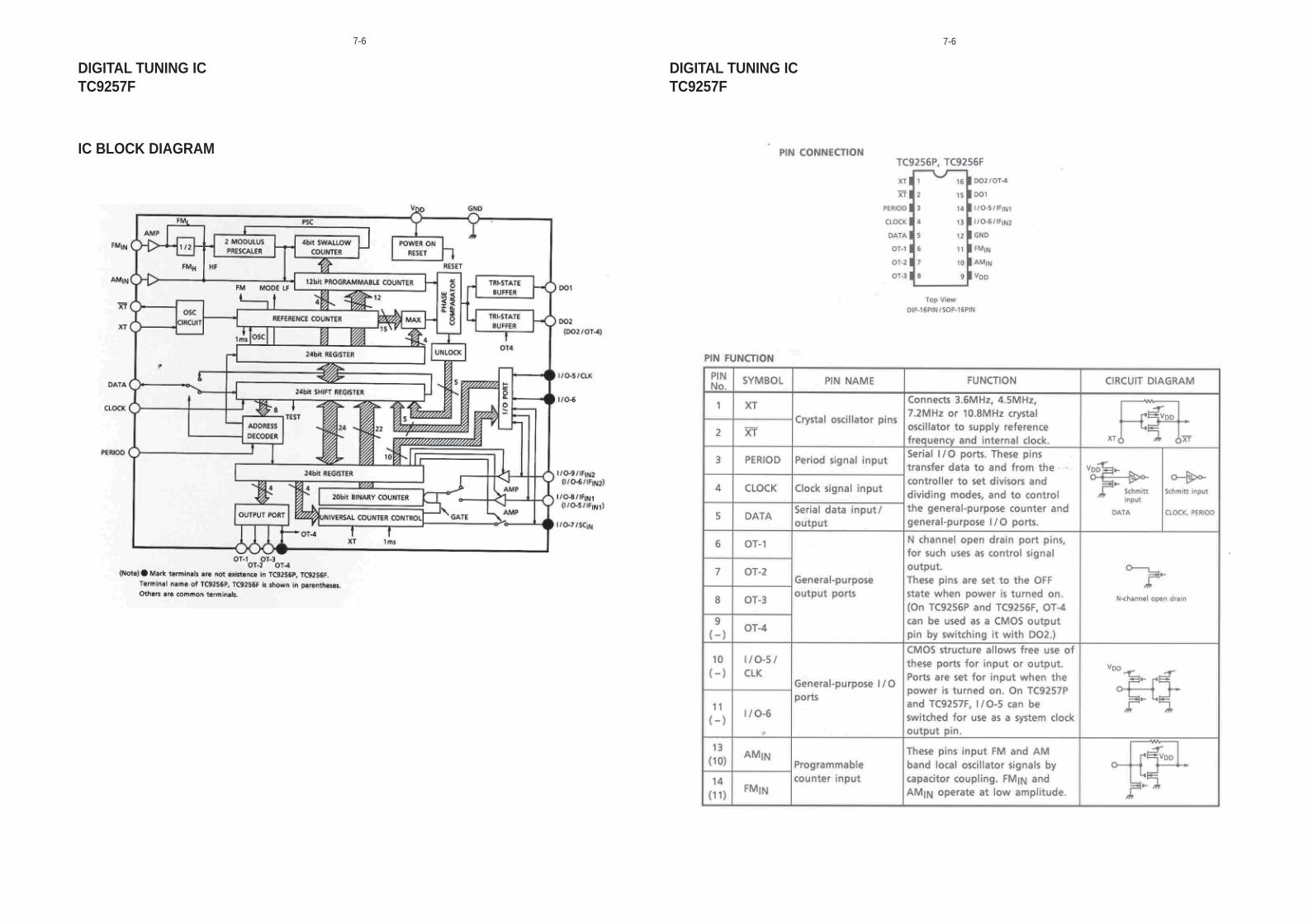
DIGITAL TUNING ICTC9257F
DIGITAL TUNING ICTC9257F
7-6 7-6
IC BLOCK DIAGRAM
7-7 7-7
DIGITAL TUNING ICTC9257F
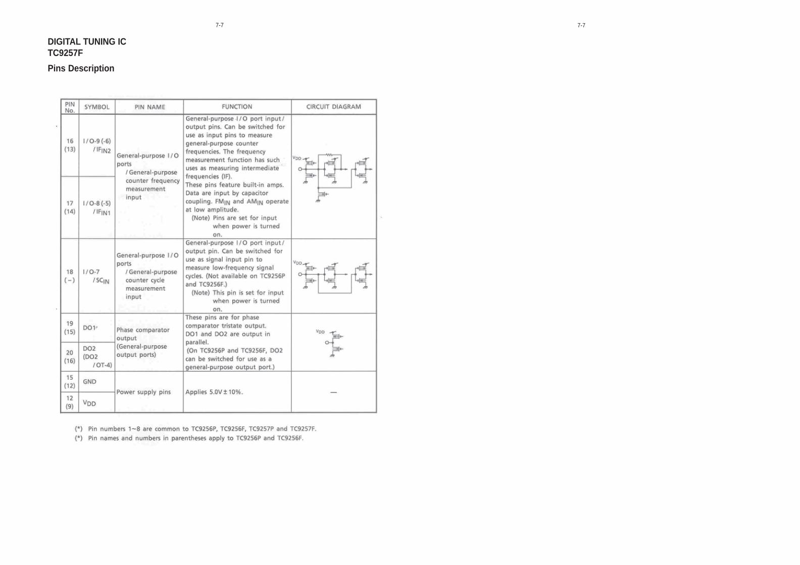
Pins Description
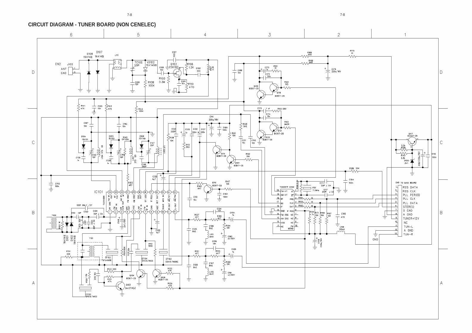
CIRCUIT DIAGRAM - TUNER BOARD (NON CENELEC)
7-8 7-8
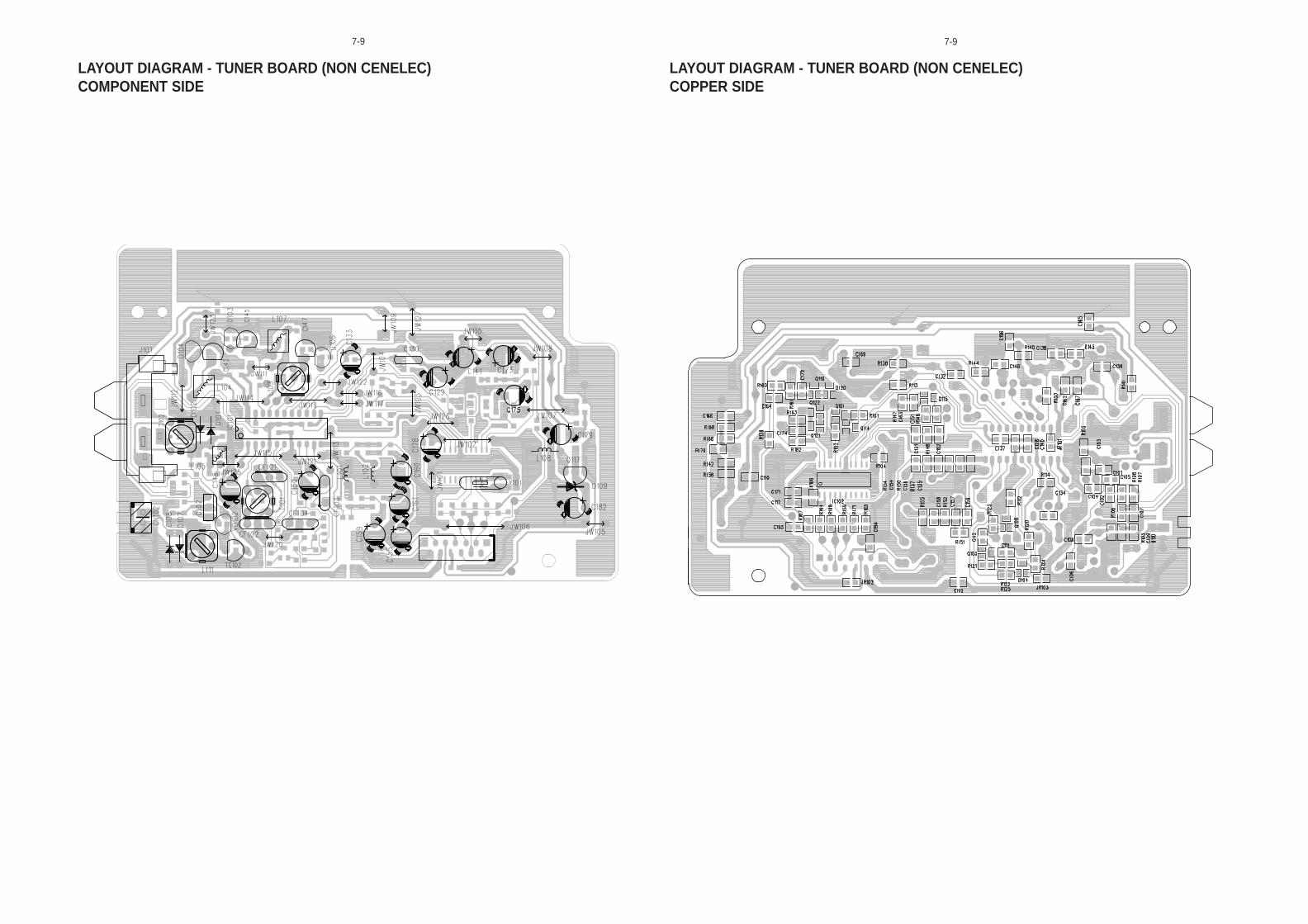
LAYOUT DIAGRAM - TUNER BOARD (NON CENELEC)COMPONENT SIDE
7-9 7-9
LAYOUT DIAGRAM - TUNER BOARD (NON CENELEC)COPPER SIDE
7-10 7-10
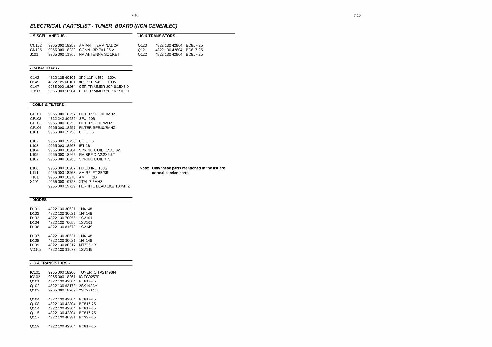
ELECTRICAL PARTSLIST - TUNER BOARD (NON CENENLEC)
- MISCELLANEOUS - - IC & TRANSISTORS -
CN102 9965 000 18259 AM ANT TERMINAL 2P Q120 4822 130 42804 BC817-25CN105 9965 000 18233 CONN 13P P=1.25 V Q121 4822 130 42804 BC817-25J101 9965 000 11365 FM ANTENNA SOCKET Q122 4822 130 42804 BC817-25
- CAPACITORS -
C142 4822 125 60101 3P0-11P N450 100VC145 4822 125 60101 3P0-11P N450 100VC147 9965 000 16264 CER TRIMMER 20P 6.15X5.9TC102 9965 000 16264 CER TRIMMER 20P 6.15X5.9
- COILS & FILTERS -
CF101 9965 000 18257 FILTER SFE10.7MHZCF102 4822 242 80989 SFU450BCF103 9965 000 18258 FILTER JT10.7MHZCF104 9965 000 18257 FILTER SFE10.7MHZL101 9965 000 19758 COIL CB
L102 9965 000 19758 COIL CBL103 9965 000 18263 IFT 2BL104 9965 000 18264 SPRING COIL 3.5XDIA5L105 9965 000 18265 FM BPF DIA2.2X6.5TL107 9965 000 18266 SPRING COIL 3T5
L108 9965 000 18267 FIXED IND 100µHL111 9965 000 18268 AM RF IFT 2B/3BT101 9965 000 18270 AM IFT 2BX101 9965 000 19728 XTAL 7.2MHZ
9965 000 19729 FERRITE BEAD 1KΩ 100MHZ
- DIODES -
D101 4822 130 30621 1N4148D102 4822 130 30621 1N4148D103 4822 130 70056 1SV101D104 4822 130 70056 1SV101D106 4822 130 81673 1SV149
D107 4822 130 30621 1N4148D108 4822 130 30621 1N4148D109 4822 130 80317 MTZJ5.1BVD102 4822 130 81673 1SV149
- IC & TRANSISTORS -
IC101 9965 000 18260 TUNER IC TA2149BNIC102 9965 000 18261 IC TC9257FQ101 4822 130 42804 BC817-25Q102 4822 130 63173 2SK192AYQ103 9965 000 18269 2SC2714O
Q104 4822 130 42804 BC817-25Q108 4822 130 42804 BC817-25Q114 4822 130 42804 BC817-25Q115 4822 130 42804 BC817-25Q117 4822 130 40981 BC337-25
Q119 4822 130 42804 BC817-25
Note: Only these parts mentioned in the list are normal service parts.
8-1
MCU & VCD BOARD
TABLE OF CONTENTS
IC Information ................................................................ 8-2 to 8-10
Circuit Diagram ......................................................................... 8-11
Layout Diagram-Component .................................................... 8-12
Layout Diagram-SMD ............................................................... 8-13
Electrical parts list .................................................................... 8-14
8-1

MICROPROCESSORTMP87EP26F
MICROPROCESSORTMP87EP26F
BLOCK DIAGRAM
8-2 8-2
PINS DESCRIPTION
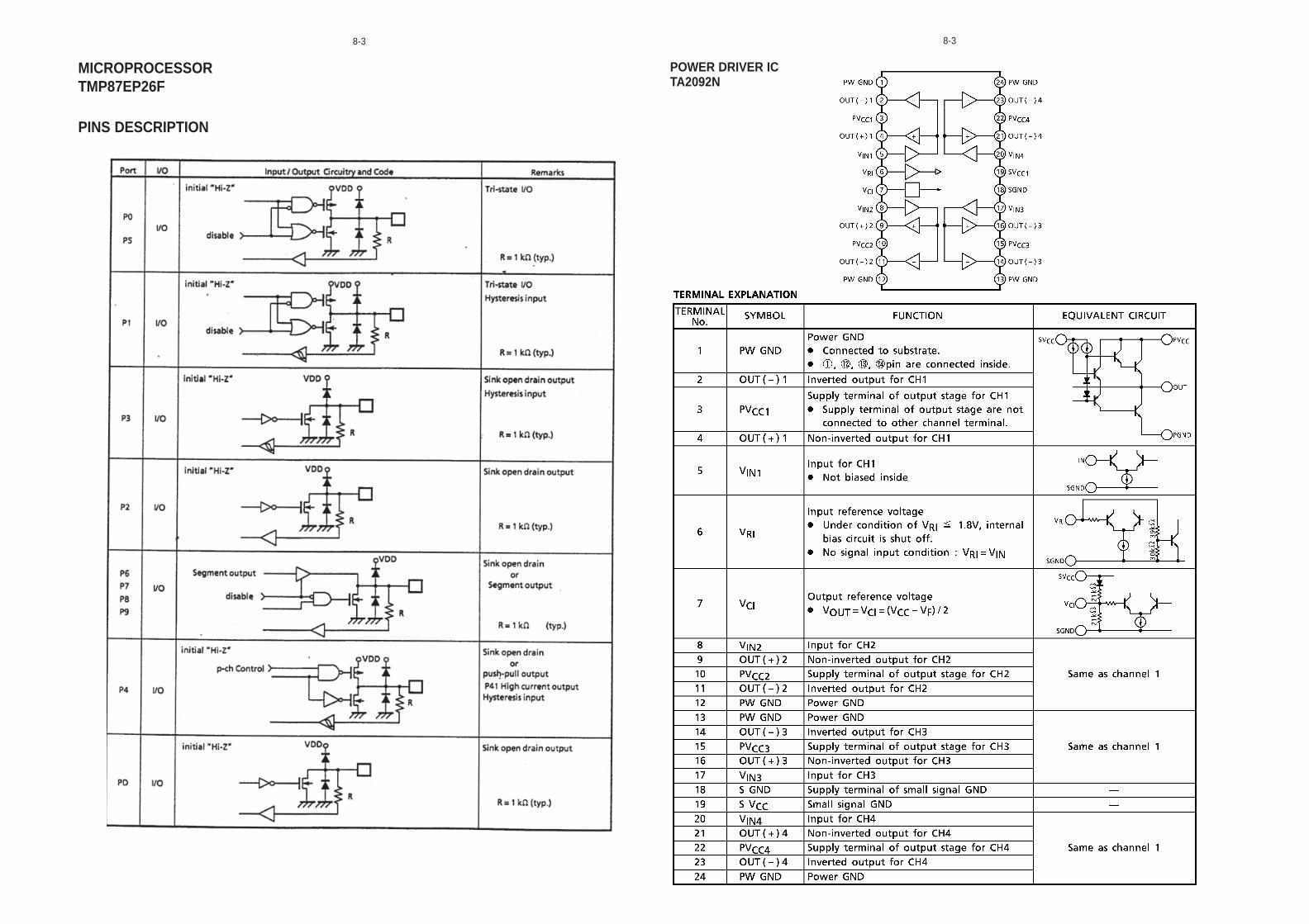
8-3 8-3
MICROPROCESSORTMP87EP26F
PINS DESCRIPTION
POWER DRIVER ICTA2092N
PIN DESCRIPTION
TSD 21 I Transmit audio data input.
TBCK 22 I Transmit audio bit clock.
RWS 23 O Dual-purpose pin. RWS is the receive audio frame sync.
SEL_PLL1 I Pins SEL_PLL[1:0] select the PLL clock frequency for the DCLK output.
RSTOUT# 24 O Reset output (active-low).
NC 27:28,65:76 No connect. Do not connect to these pins.
RSD
33
O Dual-purpose pin. RSD is the receive audio data input.
SEL_PLL0I SEL_PLL0 along with SEL_PLL1 select the PLL clock frequency for the DCLK out-
put. See the table for pin number 23.
RBCK
37
O Dual-purpose pin. RBCK is the receive audio bit clock.
SER_INI SER_IN is the serial input DSC mode.
0 = Parallel DSC mode.1 = Serial DSC mode.
VSSA 41,50:51,56:57,62:63 I Analog ground.
VREFM 42 I DAC and ADC minimum reference. Bypass to VCMR with 10 mF in parallel with 0.1 mF.
VREFP 43 I DAC and ADC maximum reference. Bypass to VCMR with 10 mF in parallel with 0.1 mF.
VCCA 44:45,59:60 I Analog VCC, 5 V.
AOR 46 O Right channel output.
AOL 47 O Left channel output.
MIC2 48 I Microphone input 2.
MIC1 49 I Microphone input 1.
VREF 52 I Internal resistor divider generates Common Mode Reference (CMR) voltage. Bypass to analog ground with 0.1 mF.
VCM 53 I ADC Common Mode Reference (CMR) buffer output. CMR is approximately 2.25 V. Bypass to analog ground with 47 mF electrolytic in parallel with 0.1 mF.
RSET 54 I Full scale DAC current adjustment.
COMP 55 I Compensation pin.
CDAC 58 O Modulated chrominance output.
YDAC 61 O Y luminance data bus for screen video port.
VDAC 64 O Composite video output.
XOUT 71 O Crystal output.
XIN 74 I 27 MHz crystal input.
PCLK 79 I/O 13.5 MHz pixel clock.
PCLK2X 80 I/O 27 MHz (2 times pixel clock).
HSYNC# 82 O Horizontal sync (active-low).
VSYNC# 84 O Vertical sync (active-low).
YUV[7:0] 86:89,92,94,96,98 I YUV data bus for screen video port.
Name Number I/O Definition
SEL_PLL1 SEL_PLL0 DCLK
0 0 Bypass PLL (input mode)
0 1 27 MHz (output mode)
1 0 32.4 MHz (output mode)
1 1 40.5 MHz (output mode)
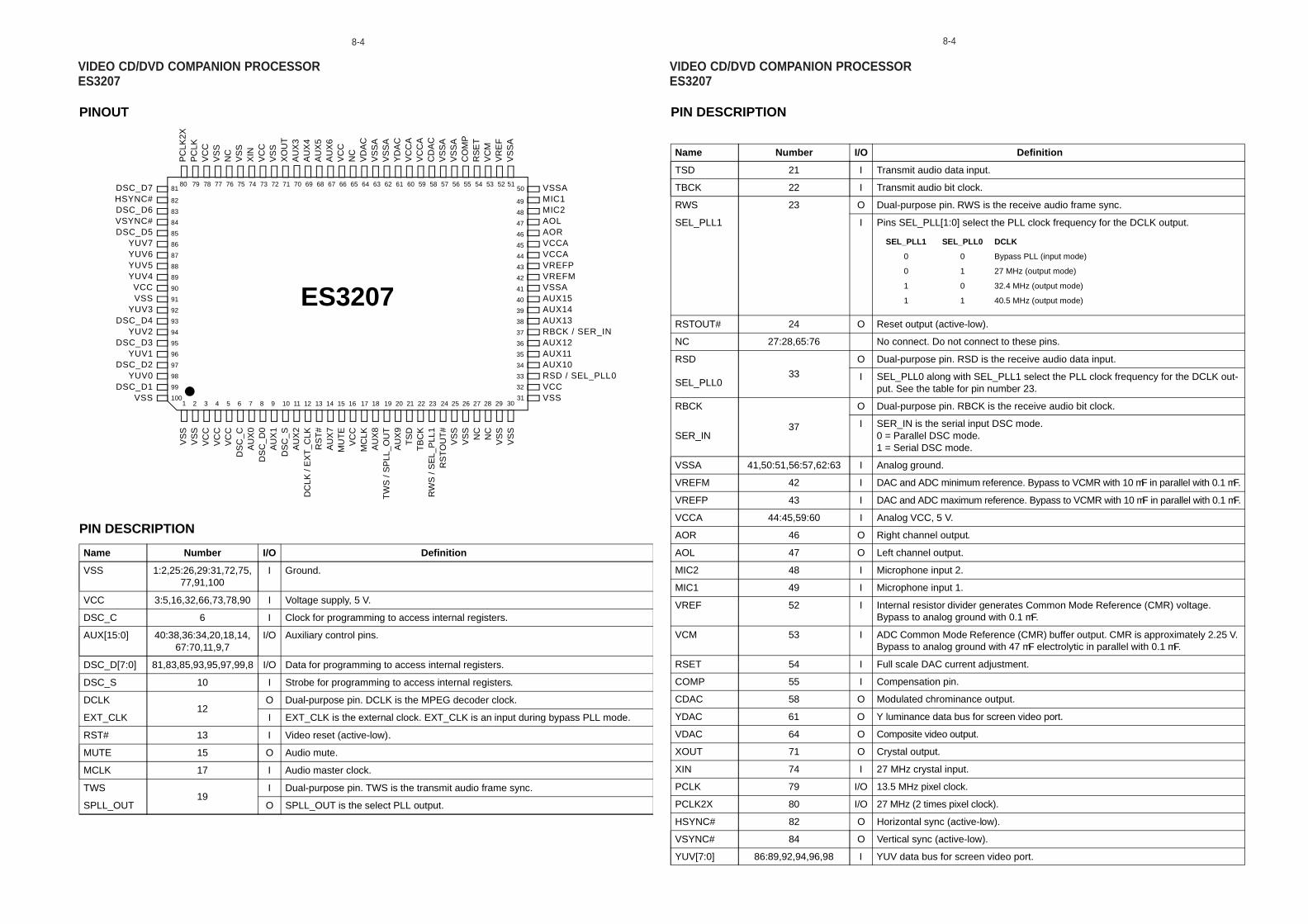
PINOUT
PIN DESCRIPTION
Name Number I/O Definition
VSS 1:2,25:26,29:31,72,75,77,91,100
I Ground.
VCC 3:5,16,32,66,73,78,90 I Voltage supply, 5 V.
DSC_C 6 I Clock for programming to access internal registers.
AUX[15:0] 40:38,36:34,20,18,14, 67:70,11,9,7
I/O Auxiliary control pins.
DSC_D[7:0] 81,83,85,93,95,97,99,8 I/O Data for programming to access internal registers.
DSC_S 10 I Strobe for programming to access internal registers.
DCLK12
O Dual-purpose pin. DCLK is the MPEG decoder clock.
EXT_CLK I EXT_CLK is the external clock. EXT_CLK is an input during bypass PLL mode.
RST# 13 I Video reset (active-low).
MUTE 15 O Audio mute.
MCLK 17 I Audio master clock.
TWS19
I Dual-purpose pin. TWS is the transmit audio frame sync.
SPLL_OUT O SPLL_OUT is the select PLL output.
1
VSSAMIC1MIC2AOLAORVCCAVCCAVREFPVREFMVSSAAUX15AUX14AUX13RBCK / SER_INAUX12AUX11AUX10RSD / SEL_PLL0VCCVSS
DSC_D7HSYNC#DSC_D6VSYNC#DSC_D5
YUV7YUV6YUV5YUV4
VCCVSS
YUV3DSC_D4
YUV2DSC_D3
YUV1DSC_D2
YUV0DSC_D1
VSST
SD
AU
X9
TW
S /
SP
LL_O
UT
AU
X8
MC
LKV
CC
MU
TE
AU
X7
RS
T#
DC
LK /
EX
T_C
LKA
UX
2D
SC
_SA
UX
1D
SC
_D0
AU
X0
DS
C_C
VC
CV
CC
VS
SV
SS
VS
SV
SS
VC
C
NC
NC
VS
SV
SS
RS
TO
UT
#R
WS
/ S
EL_
PLL
1T
BC
K
YD
AC
VS
SA
VS
SA
VD
AC
NC
VC
CA
UX
6A
UX
5A
UX
4A
UX
3X
OU
TV
SS
VC
CX
INV
SS
NC
VS
SV
CC
PC
LKP
CLK
2X
VS
SA
VR
EF
VC
MR
SE
TC
OM
PV
SS
AV
SS
AC
DA
CV
CC
AV
CC
A31
30
5150
8081
1002 3 4 5 6 7 8 9 10 11 12 13 14 15 16 17 18 19 20 21 22 23 24 25 26 27 28 29
49
48
47
46
45
44
43
42
41
40
39
38
37
36
35
34
33
32
79 78 77 76 75 74 73 72 71 70 69 68 67 66 65 64 63 62 61 60 59 58 57 56 55 54 53 52
82
83
84
85
86
87
88
89
90
91
92
93
94
95
96
97
98
99
ES3207
VIDEO CD/DVD COMPANION PROCESSORES3207
VIDEO CD/DVD COMPANION PROCESSORES3207
8-4 8-4
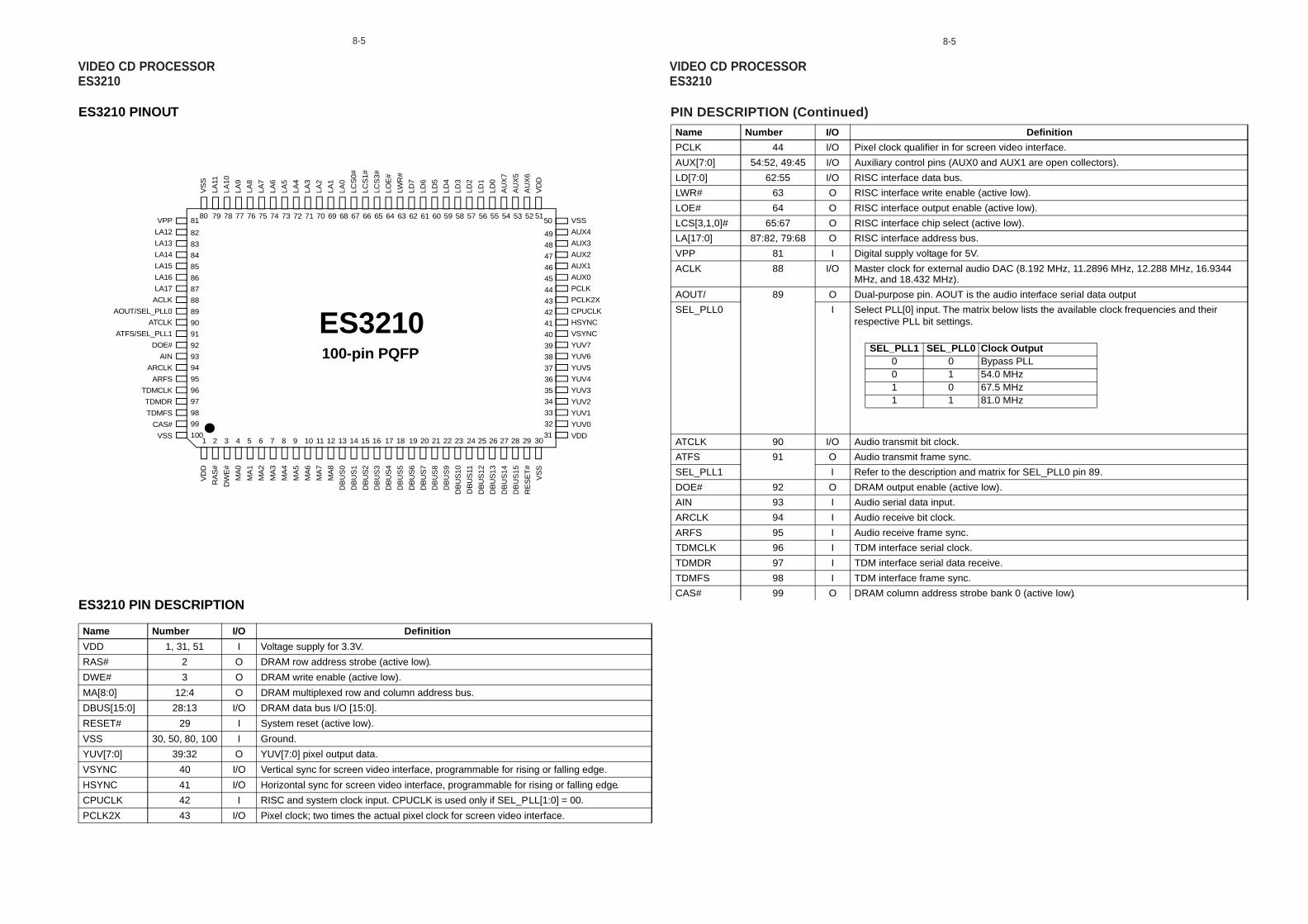
ES3210 PINOUT
ES3210 PIN DESCRIPTION
1
VSS
AUX4
AUX3
AUX2
AUX1
AUX0
PCLK
PCLK2X
CPUCLK
HSYNC
VSYNC
YUV7
YUV6
YUV5
YUV4
YUV3
YUV2
YUV1
YUV0
VDD
VPP
LA12
LA13
LA14
LA15
LA16
LA17
ACLK
AOUT/SEL_PLL0
ATCLK
ATFS/SEL_PLL1
DOE#
AIN
ARCLK
ARFS
TDMCLK
TDMDR
TDMFS
CAS#
VSSD
BU
S8
DB
US
7
DB
US
6
DB
US
5
DB
US
4
DB
US
3
DB
US
2
DB
US
1
DB
US
0
MA
8
MA
7
MA
6
MA
5
MA
4
MA
3
MA
2
MA
1
MA
0
RA
S#
VD
D
VS
S
RE
SE
T#
DW
E#
DB
US
14
DB
US
15
DB
US
13
DB
US
12
DB
US
11
DB
US
10
DB
US
9
LD6
LD7
LWR
#
LOE
#
LCS
3#
LCS
1#
LCS
0#
LA0
LA1
LA2
LA3
LA4
LA5
LA6
LA7
LA8
LA9
LA10
LA11
VS
S
VD
D
AU
X6
AU
X5
AU
X7
LD0
LD1
LD2
LD3
LD4
LD5
3130
5150
8081
1002 3 4 5 6 7 8 9 10 11 12 13 14 15 16 17 18 19 20 21 22 23 24 25 26 27 28 29
49
48
47
46
45
44
43
42
41
40
39
38
37
36
35
34
33
32
79 78 77 76 75 74 73 72 71 70 69 68 67 66 65 64 63 62 61 60 59 58 57 56 55 54 53 52
82
83
84
85
86
87
88
89
90
91
92
93
94
95
96
97
98
99
ES3210100-pin PQFP
Name Number I/O Definition
VDD 1, 31, 51 I Voltage supply for 3.3V.
RAS# 2 O DRAM row address strobe (active low).
DWE# 3 O DRAM write enable (active low).
MA[8:0] 12:4 O DRAM multiplexed row and column address bus.
DBUS[15:0] 28:13 I/O DRAM data bus I/O [15:0].
RESET# 29 I System reset (active low).
VSS 30, 50, 80, 100 I Ground.
YUV[7:0] 39:32 O YUV[7:0] pixel output data.
VSYNC 40 I/O Vertical sync for screen video interface, programmable for rising or falling edge.
HSYNC 41 I/O Horizontal sync for screen video interface, programmable for rising or falling edge.
CPUCLK 42 I RISC and system clock input. CPUCLK is used only if SEL_PLL[1:0] = 00.
PCLK2X 43 I/O Pixel clock; two times the actual pixel clock for screen video interface.
PCLK 44 I/O Pixel clock qualifier in for screen video interface.
AUX[7:0] 54:52, 49:45 I/O Auxiliary control pins (AUX0 and AUX1 are open collectors).
LD[7:0] 62:55 I/O RISC interface data bus.
LWR# 63 O RISC interface write enable (active low).
LOE# 64 O RISC interface output enable (active low).
LCS[3,1,0]# 65:67 O RISC interface chip select (active low).
LA[17:0] 87:82, 79:68 O RISC interface address bus.
VPP 81 I Digital supply voltage for 5V.
ACLK 88 I/O Master clock for external audio DAC (8.192 MHz, 11.2896 MHz, 12.288 MHz, 16.9344 MHz, and 18.432 MHz).
AOUT/ 89 O Dual-purpose pin. AOUT is the audio interface serial data output
SEL_PLL0 I Select PLL[0] input. The matrix below lists the available clock frequencies and their respective PLL bit settings.
ATCLK 90 I/O Audio transmit bit clock.
ATFS 91 O Audio transmit frame sync.
SEL_PLL1 I Refer to the description and matrix for SEL_PLL0 pin 89.
DOE# 92 O DRAM output enable (active low).
AIN 93 I Audio serial data input.
ARCLK 94 I Audio receive bit clock.
ARFS 95 I Audio receive frame sync.
TDMCLK 96 I TDM interface serial clock.
TDMDR 97 I TDM interface serial data receive.
TDMFS 98 I TDM interface frame sync.
CAS# 99 O DRAM column address strobe bank 0 (active low).
Name Number I/O Definition
SEL_PLL1 SEL_PLL0 Clock Output0 0 Bypass PLL0 1 54.0 MHz1 0 67.5 MHz1 1 81.0 MHz
PIN DESCRIPTION (Continued)
VIDEO CD PROCESSORES3210
VIDEO CD PROCESSORES3210
8-5 8-5

DIGITAL SERVO PROCESSORTC9462F
BLOCK DIAGRAM
8-6 8-6
DIGITAL SERVO PROCESSORTC9462F
DIGITAL SERVO PROCESSORTC9462F
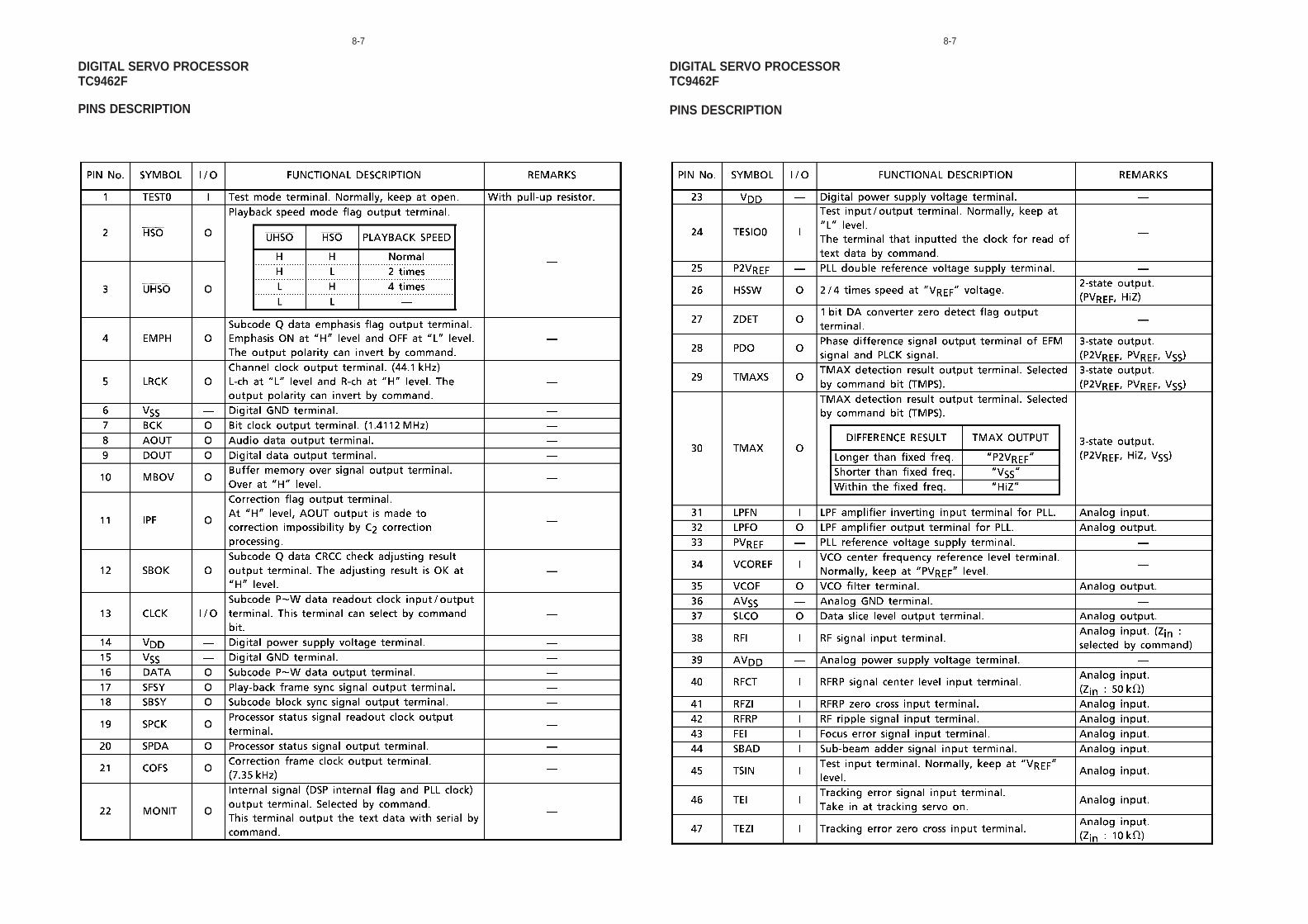
PINS DESCRIPTION PINS DESCRIPTION
8-7 8-7
DIGITAL SERVO PROCESSORTC9462F
PINS DESCRIPTION
DIGITAL SERVO PROCESSORTC9462F
PINS DESCRIPTION
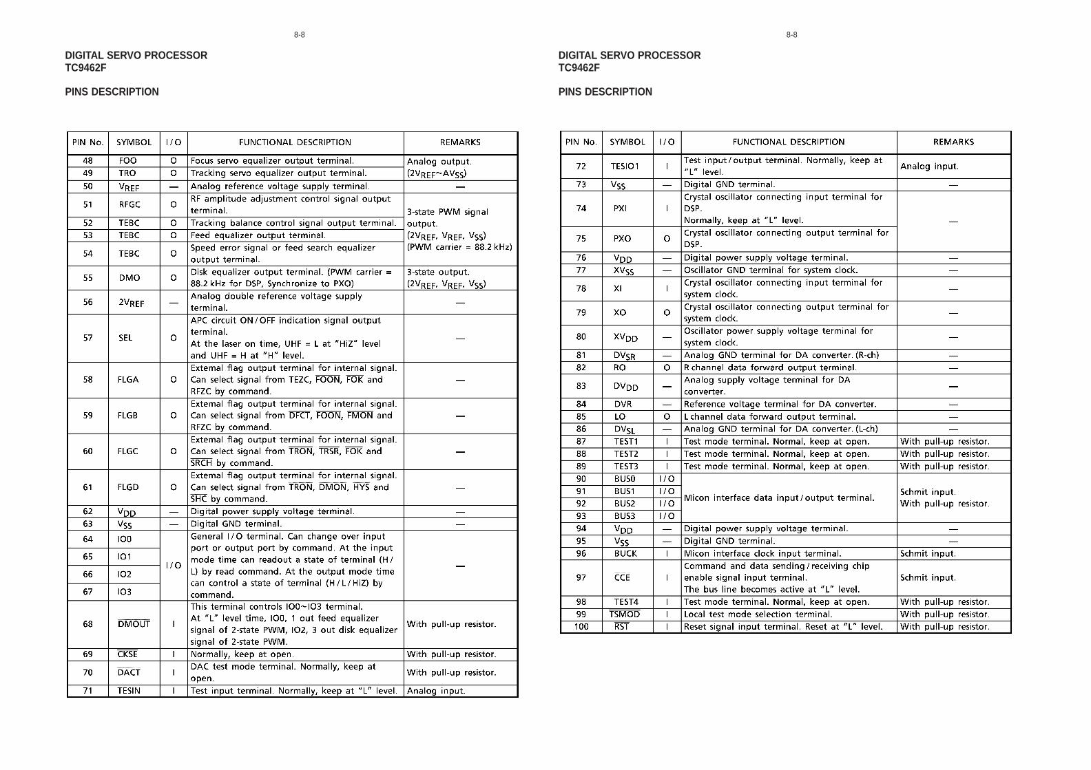
8-8 8-8

PIN CONFIGURATIONS
Q5
OE
A10
Q7
Q6
A13
A8
A9
A11
PGM
A17
Q0
A0
A2
A3
A4
A5
A6
A7
A12
A15
A16
A14
A1
VccVpp 1
2
3
4
5
6
7
8
9
10
11
12
13
14
15
16
30
31
32
25
26
27
28
29
20
21
22
23
24
19
18
17 Q3
Q4
GND
Q2
CE
Q1
32-pin DIP
BLOCK DIAGRAM
CONTROLOUTPUT
BUFFER
DECODER
CORE
ARRAY
Q0
Q7
.CE
OE
A0
.
PGM
V
GND
CC
VPP
A17
PIN DESCRIPTION
SYMBOL DESCRIPTION
A0−A17 Address Inputs
Q0−Q7 Data Inputs/Outputs
CE Chip Enable
OE Output Enable
PGM Program Enable
VPP Program/Erase Supply Voltage
VCC Power Supply
GND Ground
DRAMT224162B28S
E2PROMW27C020
8-9 8-9
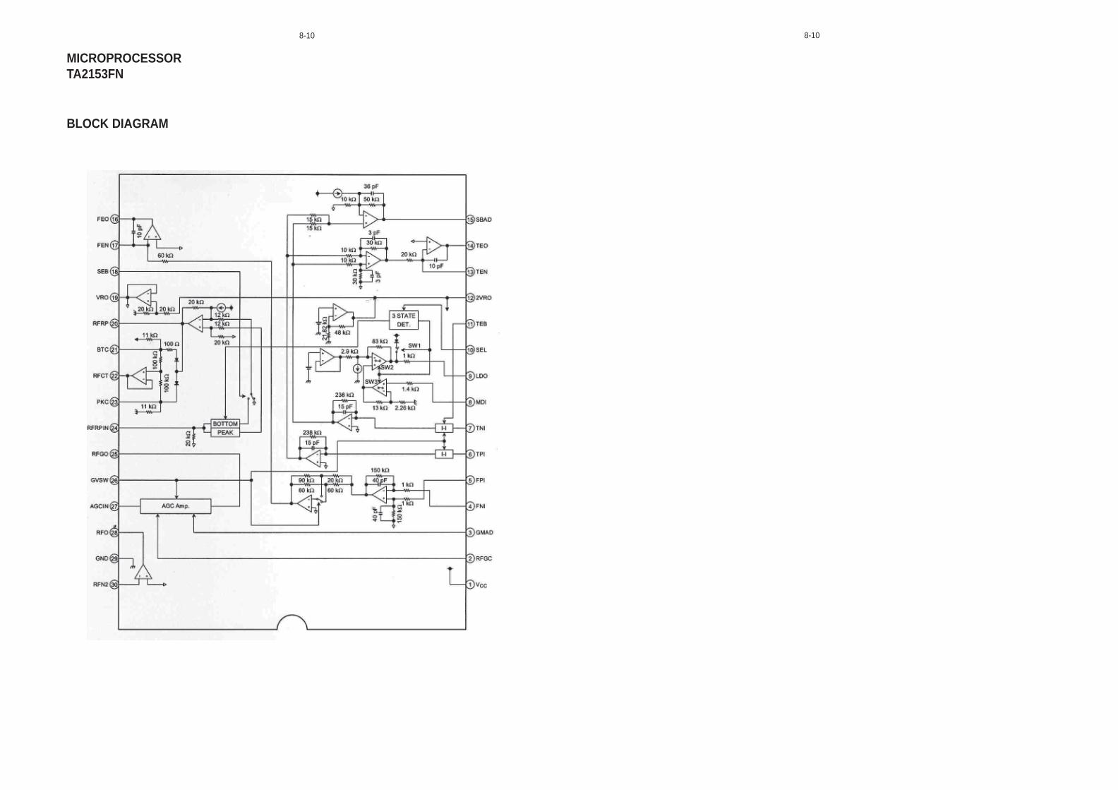
MICROPROCESSORTA2153FN
BLOCK DIAGRAM
8-10 8-10

CIRCUIT DIAGRAM - MCU & VCD BOARD
8-11 8-11
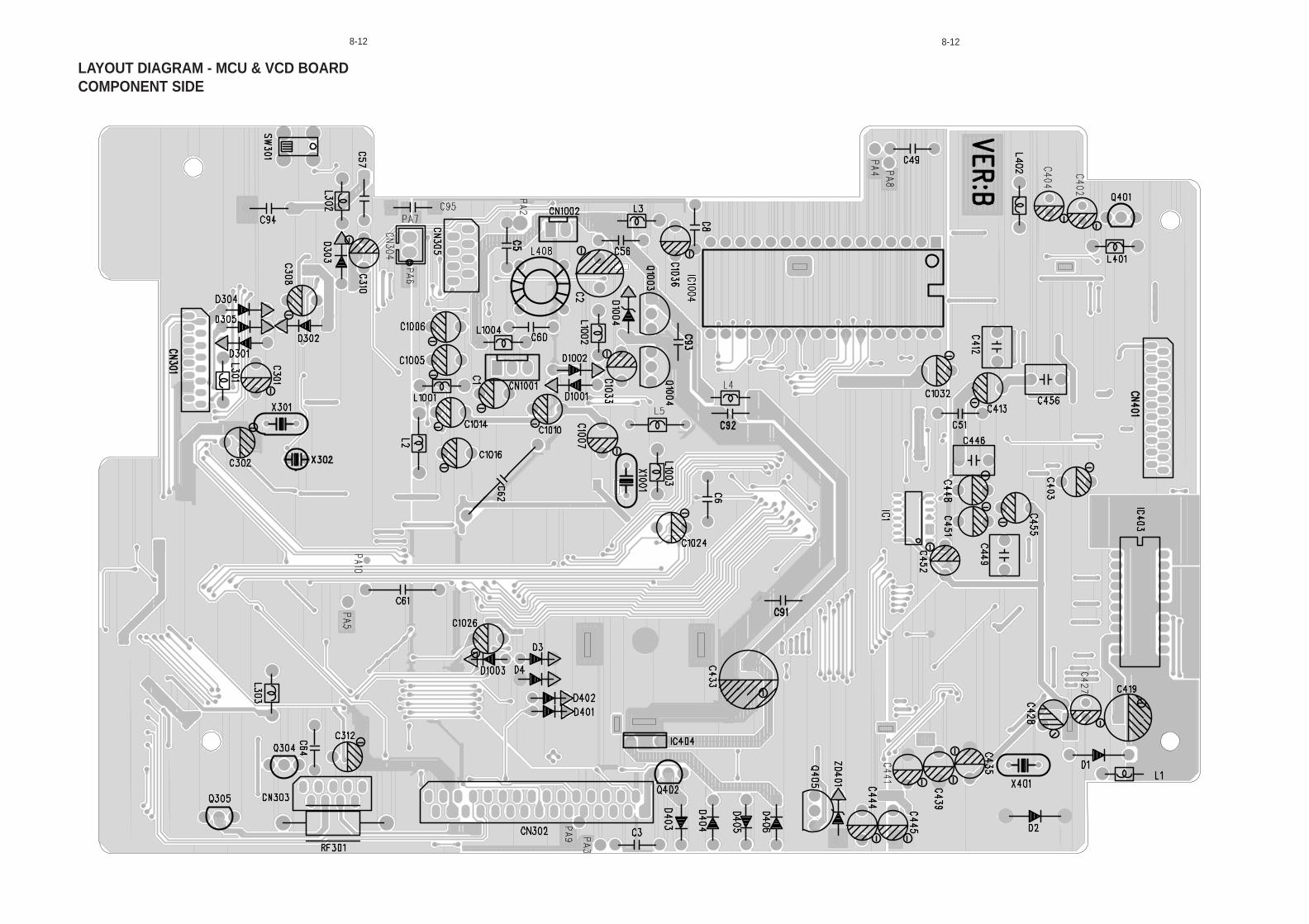
LAYOUT DIAGRAM - MCU & VCD BOARDCOMPONENT SIDE
8-12 8-12
8-13 8-13
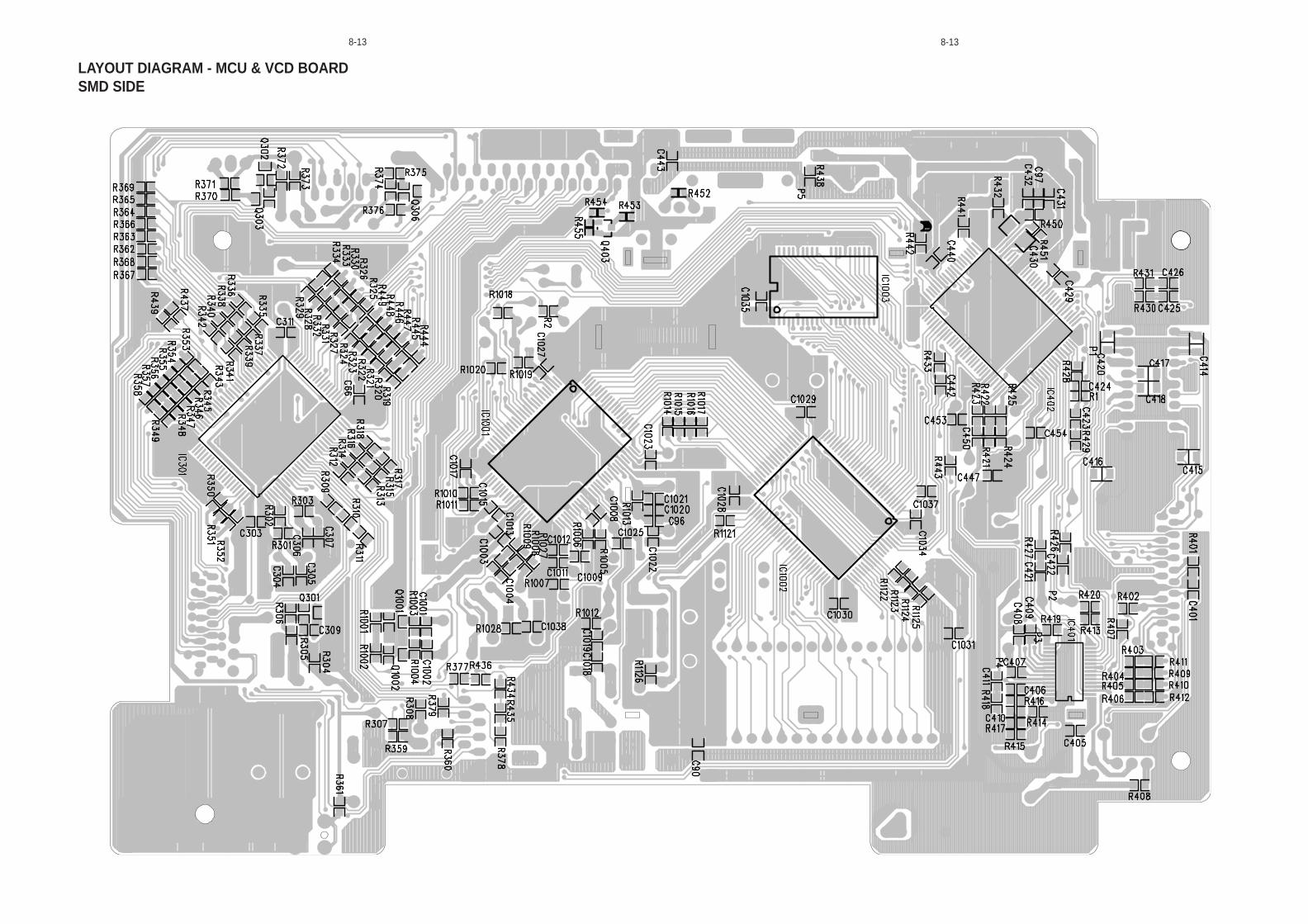
LAYOUT DIAGRAM - MCU & VCD BOARDSMD SIDE

8-14 8-14
- MISCELLANEOUS - - DIODES -
CN1001 9965 000 20205 CONN BASE 3P D405 4822 130 83883 FR202CN1002 9965 000 20206 CONNECTOR BASE 2P D406 4822 130 83883 FR202CN301 9965 000 18230 CONN 16P H P=1.0 ZD401 4822 130 83206 BZX79-B5V6CN302 9965 000 18232 CONN 30P P=1.25 VCN303 9965 000 18273 CONN 9P
- IC & TRANSISTORS -CN401 9965 000 18274 CONN 22PSW301 9965 000 18285 SWITCH SIDE SPVF130100 IC1001 9965 000 19731 IC ES3207FPPA4 9965 000 20208 WIRE 2P IC1002 9965 000 19732 IC ES3210FMPA5 9965 000 20209 WIRE 2P IC1003 9965 000 19734 IC T224162B-28SPA7 9965 000 14709 TERMINAL PIN IC1004 9965 000 14729 E2PROM W27C020
IC301 9965 000 18275 IC MCU TMP87EP26F4K76
- RESISTORS - IC401 9322 171 88668 IC SM TA2153FN (TOSJ) RIC402 9965 000 18276 IC TC9462F
RF301 9965 000 14537 1/2W 1Ω IC403 9965 000 18277 IC TA2092NIC404 4822 209 80817 L7805CVQ1001 5322 130 60159 BC846B
- COILS & FILTERS -Q1002 5322 130 60159 BC846B
L1001 9965 000 19740 FIXED IND 100µH TP=52MM Q1003 4822 130 40981 BC337-25L1002 9965 000 19760 FIXED IND 2.4µH (K) Q1004 4822 130 40981 BC337-25L1003 9965 000 19761 FIXED IND 3.3µH CECS Q301 5322 130 60159 BC846BL1004 9965 000 19762 FIXED IND 10µH Q302 5322 130 60159 BC846BL2 9965 000 14721 FILTER EMI BL01 RN1
Q303 5322 130 60159 BC846BL301 9965 000 19740 FIXED IND 100µH TP=52MM Q304 5322 130 44593 BC369L302 9965 000 19740 FIXED IND 100µH TP=52MM Q305 5322 130 44593 BC369L303 9965 000 19740 FIXED IND 100µH TP=52MM Q306 4822 130 60373 BC856BL401 9965 000 19762 FIXED IND 10µH Q401 4822 130 44568 BC557BL402 9965 000 19763 FIXED IND 47µH (K) T26
Q402 5322 130 44593 BC369L408 9965 000 20207 FIL EMI Q403 5322 130 60159 BC846BX1001 9965 000 19764 XTAL 27MHZ Q405 4822 130 40981 BC337-25X301 9965 000 18282 CRYSTAL 7.3728 MHZX302 9965 000 18283 CRYSTAL 32.768KHZX401 9965 000 19766 XTAL 16.93MHZ
- DIODES -
D1 4822 130 31878 1N4003GD1001 4822 130 30621 1N4148D1002 4822 130 30621 1N4148D1003 4822 130 30621 1N4148D1004 4822 130 31554 BZX79-B4V3
D2 4822 130 31878 1N4003GD3 4822 130 30621 1N4148D301 4822 130 30621 1N4148D302 4822 130 30621 1N4148 Note: Only these parts mentioned in the list areD303 4822 130 30621 1N4148 normal service parts.
D305 4822 130 30621 1N4148D4 4822 130 30621 1N4148D401 4822 130 30621 1N4148D402 4822 130 30621 1N4148D403 4822 130 83883 FR202
D404 4822 130 83883 FR202
ELECTRICAL PARTSLIST - VCD MCU BOARD
!
DIODE & CONNECTIONBOARDS
TABLE OF CONTENTS
Diode Board - Circuit Diagram ........................................ 9 -1
Diode Board - Layout Diagram........................................ 9 -1
Conn. Board - Circuit Diagram ........................................ 9 -2
Conn. Board - Layout Diagram....................................... 9-3
Electrical Parts List ......................................................... 9-4
9-1 9-1
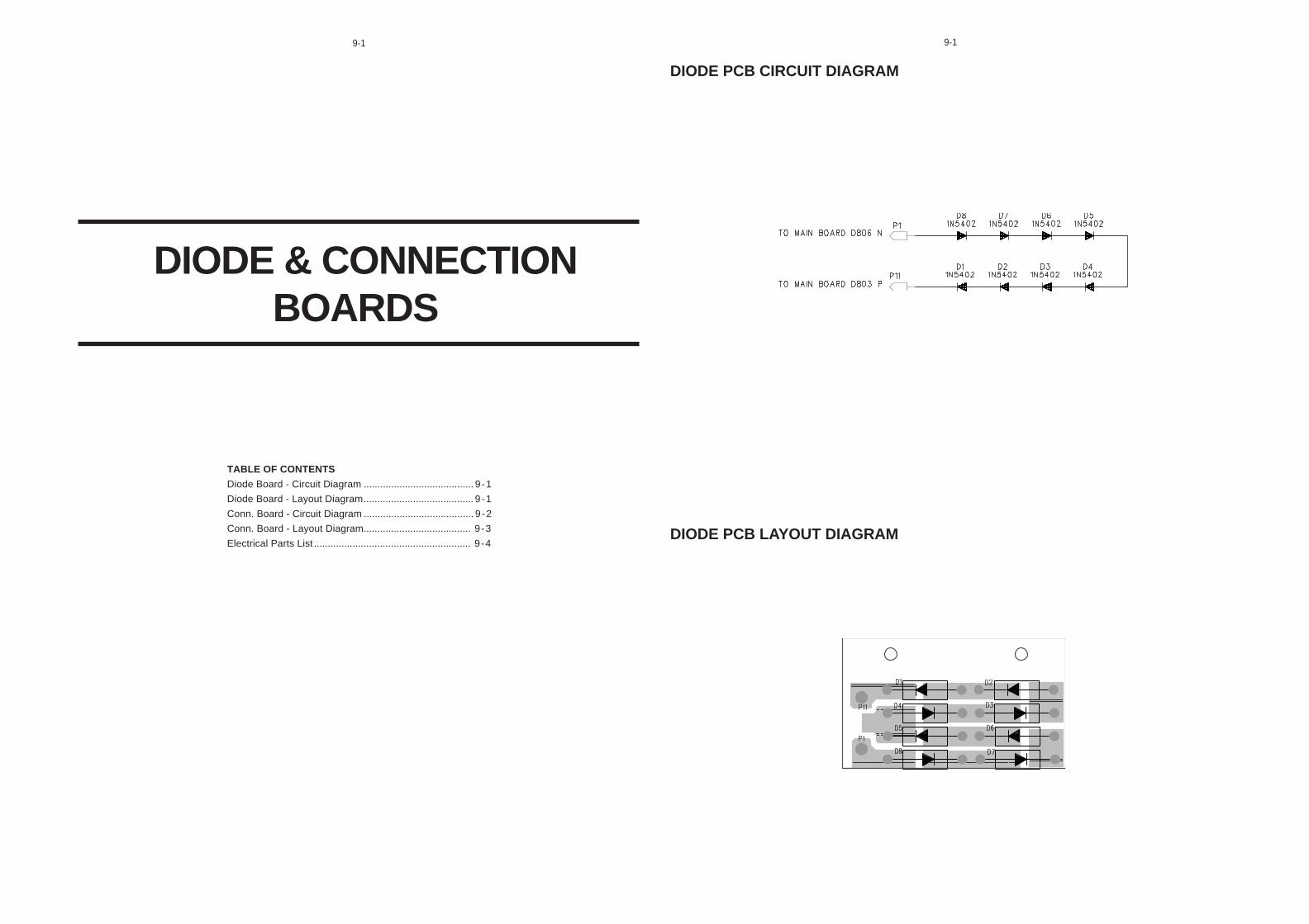
DIODE PCB LAYOUT DIAGRAM
DIODE PCB CIRCUIT DIAGRAM
9-2 9-2
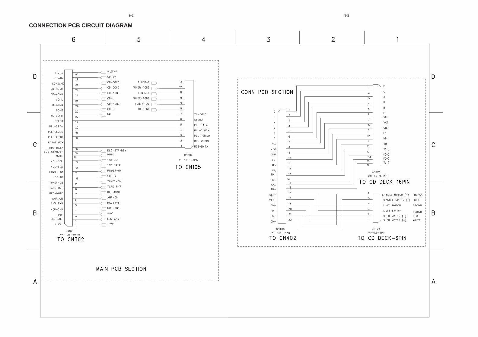
CONNECTION PCB CIRCUIT DIAGRAM
9-3 9-3
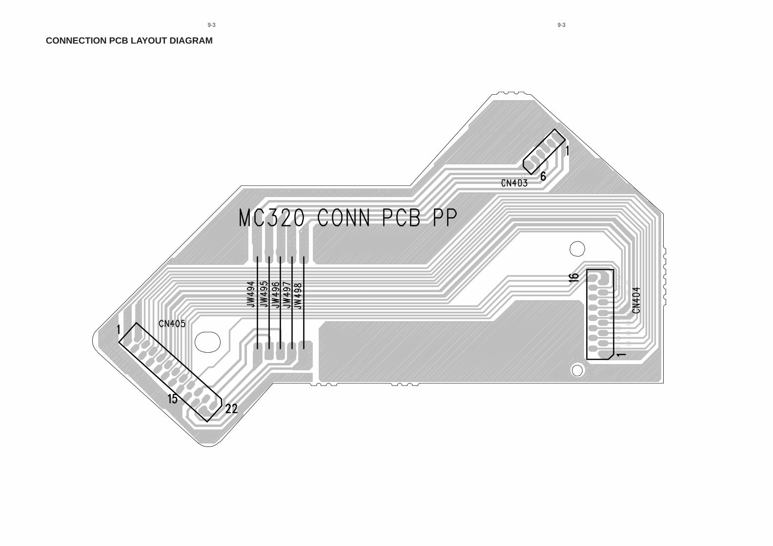
CONNECTION PCB LAYOUT DIAGRAM
9-4 9-4
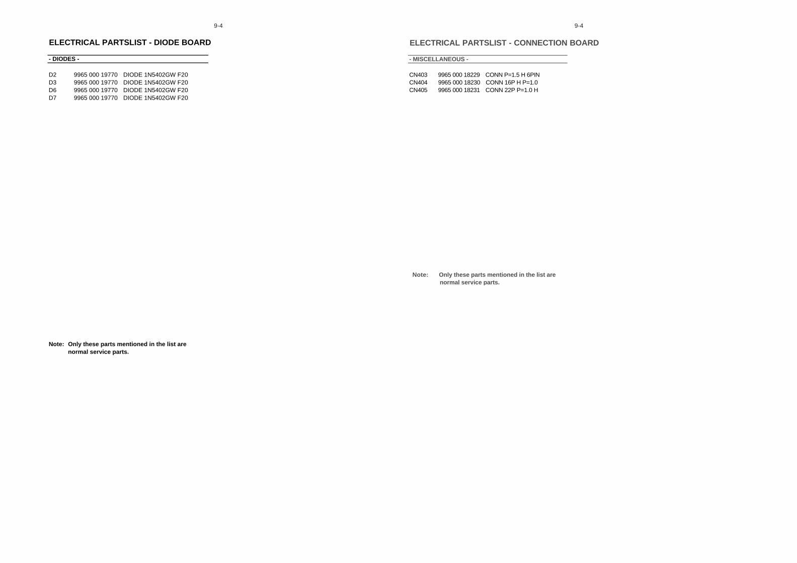
ELECTRICAL PARTSLIST - CONNECTION BOARD
- MISCELLANEOUS -
CN403 9965 000 18229 CONN P=1.5 H 6PINCN404 9965 000 18230 CONN 16P H P=1.0CN405 9965 000 18231 CONN 22P P=1.0 H
Note: Only these parts mentioned in the list are normal service parts.
ELECTRICAL PARTSLIST - DIODE BOARD
- DIODES -
D2 9965 000 19770 DIODE 1N5402GW F20D3 9965 000 19770 DIODE 1N5402GW F20D6 9965 000 19770 DIODE 1N5402GW F20D7 9965 000 19770 DIODE 1N5402GW F20
Note: Only these parts mentioned in the list are normal service parts.
10-1
MAIN BOARD
TABLE OF CONTENTS
IC Block Diagram ......................................................... 10-2 to 10-3
Circuit Diagram - Main Part ...................................................... 10-4
Circuit Diagram - Tape Part ..................................................... 10-5
Component Layout - Main PCB ................................................. 10-6
SMD Layout - Main PCB .......................................................... 10-7
Electrical Parts List ................................................................... 10-8
10-1
Block diagram
Internal circuit configuration
TAPE HEAD SWITCHING ICBA3126N
TDA7468 INTERNAL BLOCK DIAGRAM
VOLUME I
RIGHTSUR.
SOURCE
SUPPLYPOWER
SELECTOR
TREBLE
LEFT
VOLUME II
LOGIC
LEFT
REC
IIC BUS
BASS ALC
BASS
LEFT
VOLUME I
LEFTSUR.
TREBLE
RIGHT
VOLUME II
RIGHT
BASS
RIGHT
17
14
15
9
20
1
13
28
3
26
4
25
5
24
6
23
8
21
2
7
22
12
TDA7468
16
10
19
11
18
27
IC BLOCK DIAGRAMTDA7468
10-2 10-2
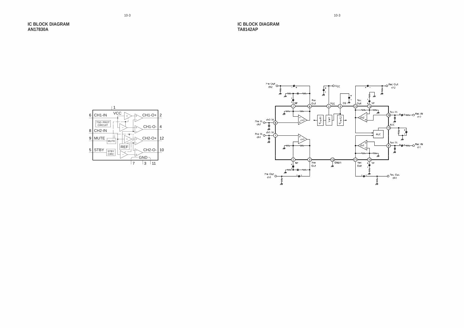
IC BLOCK DIAGRAMAN17830A
IC BLOCK DIAGRAMTA8142AP
STBYCIRC
MUTE
TSD PROTCIRCUIT
REF
GND
CH1-O- 4CH2-IN8
CH2-O+ 12
CH2-O- 10
3 117
MUTE9
STBY5
VCC
1
CH1-IN6 CH1-O+ 2
10-3 10-3
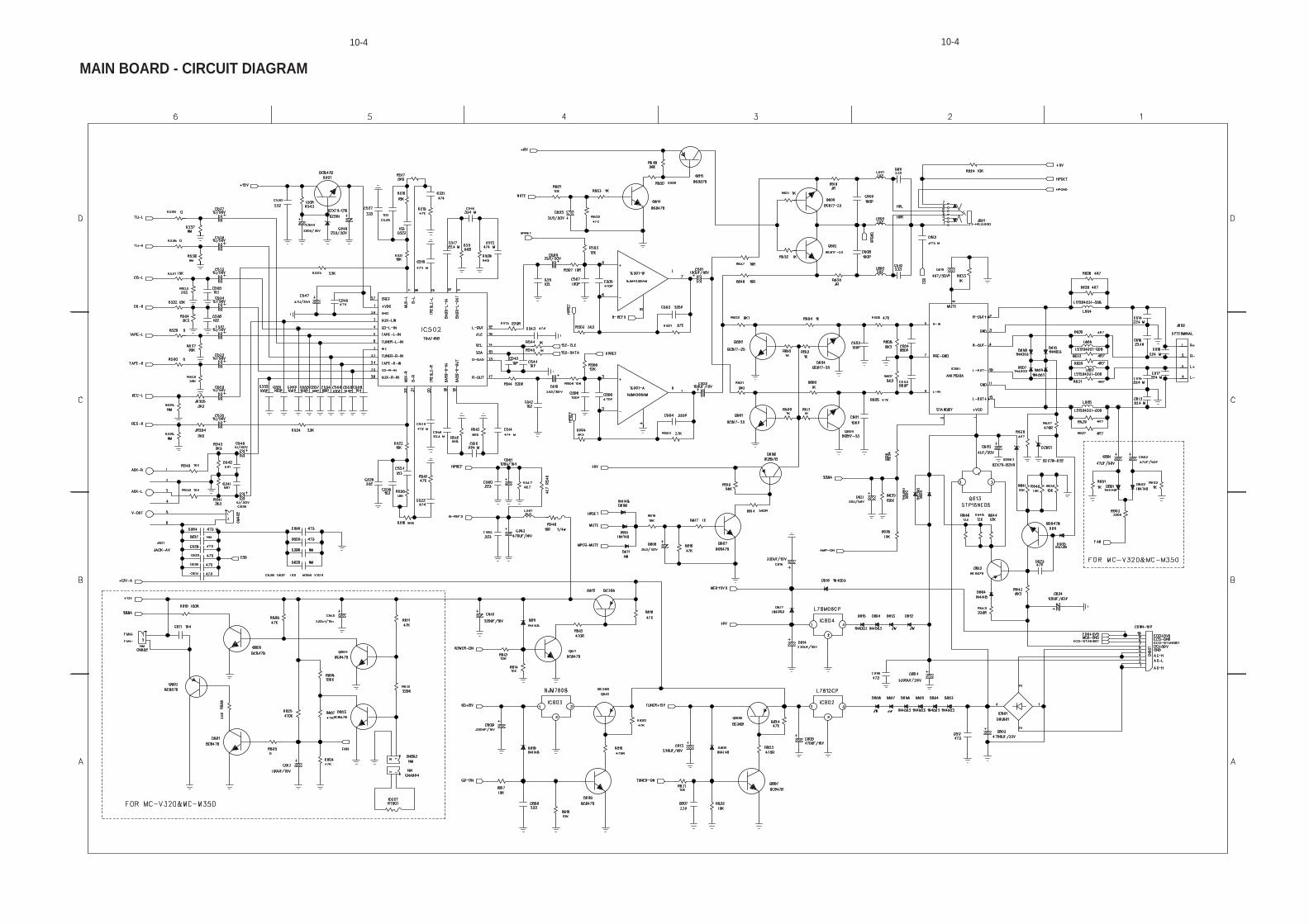
MAIN BOARD - CIRCUIT DIAGRAM
10-410-4
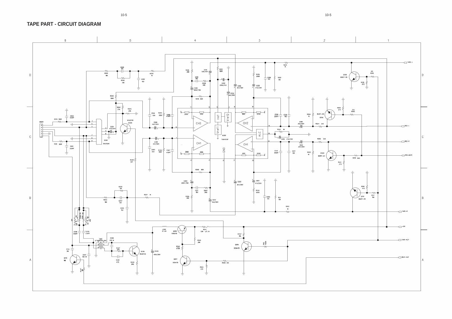
10-5 10-5
TAPE PART - CIRCUIT DIAGRAM
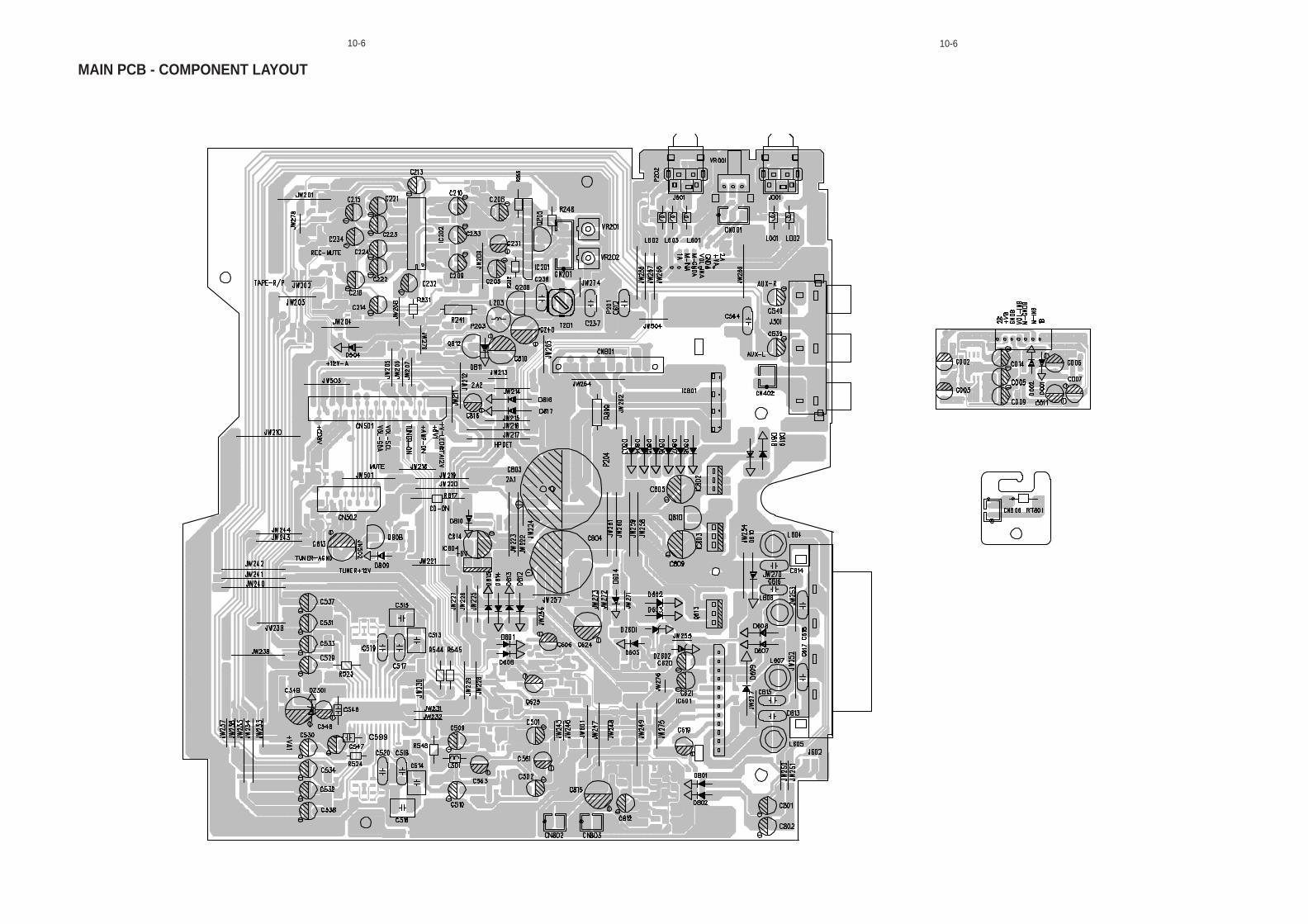
MAIN PCB - COMPONENT LAYOUT
10-6 10-6
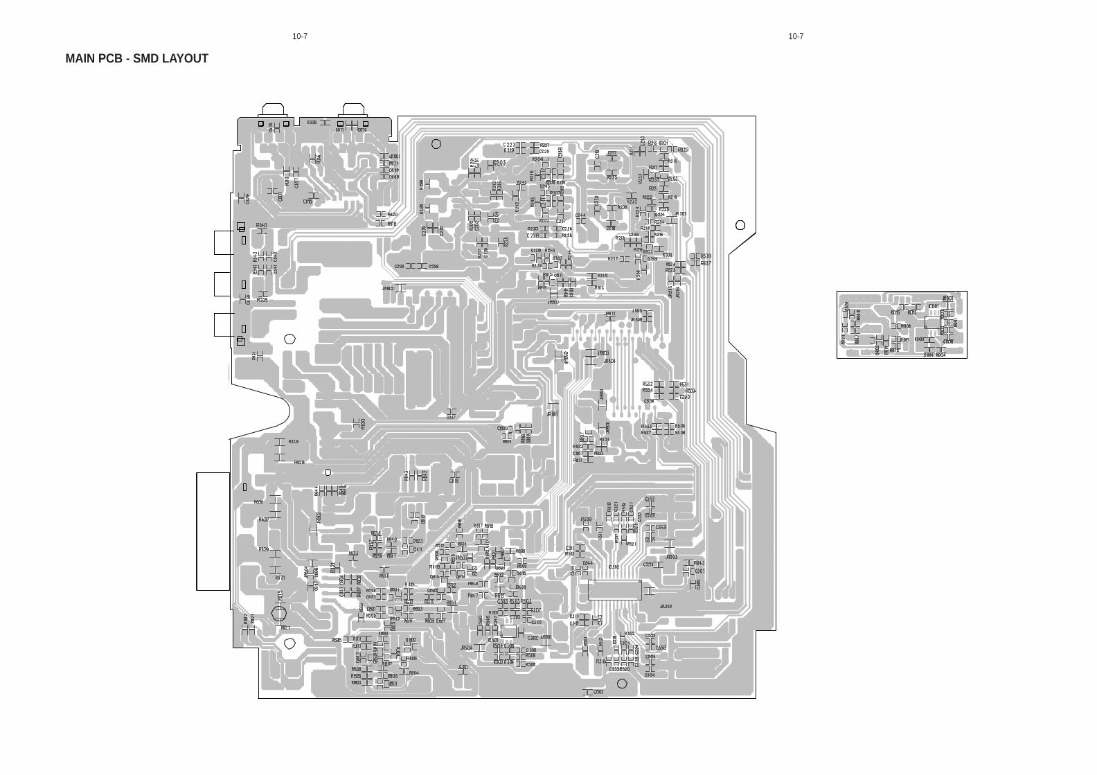
MAIN PCB - SMD LAYOUT
10-7 10-7

10-8 10-8
ELECTRICAL PARTSLIST - MAIN BOARD
- MISCELLANEOUS - - DIODES -
CN001 9965 000 20199 WIRE ASS'Y 3PIN D610 4822 130 31878 1N4003GCN201 9965 000 14509 CON BASE 6P D801 4822 130 30621 1N4148CN402 9965 000 20200 WIRE ASS'Y 2PIN D802 4822 130 30621 1N4148CN403 9965 000 18229 CONN P=1.5 H 6PIN D809 4822 130 30621 1N4148CN404 9965 000 18230 CONN 16P H P=1.0 D810 4822 130 30621 1N4148
CN405 9965 000 18231 CONN 22P P=1.0 H D811 4822 130 30621 1N4148CN501 9965 000 18232 CONN 30P P=1.25 V D814 4822 130 31878 1N4003GCN502 9965 000 18233 CONN 13P P=1.25 V D815 4822 130 31878 1N4003GCN801 9965 000 18234 WIRE ASS'Y 10P L170MM D816 4822 130 31878 1N4003GCN802 9965 000 19716 CONNECTOR BASE 2P D817 4822 130 31878 1N4003G
CN803 9965 000 19717 WIRE ASS'Y 2PIN L=250MM DZ501 4822 130 61219 BZX79-B10CN806 9965 000 19718 CONNECTOR 2P PH-2A DZ601 4822 130 34441 BZX79-B22J001 9965 000 20201 HEAD PHONE JACK D3.5MM DZ602 4822 130 31981 BZX79-B3V9J501 9965 000 20202 JACK-AC 3 MC-350J601 9965 000 20201 HEAD PHONE JACK D3.5MM
- IC & TRANSISTORS -J602 9965 000 18239 SPK TERMINAL 4P 94V0VR001 9965 000 20204 VOL 50KA IC001 5322 209 15853 NJM4556AMZA1 9965 000 14709 TERMINAL PIN IC201 4822 209 30188 BA3126N
IC202 4822 209 32082 TA8142APIC501 5322 209 15853 NJM4556AM
- RESISTORS - IC502 9322 150 74668 IC SM TDA7468D (ST00) R
R241 9965 000 18241 FUSE RES 33Ω 1/2W IC601 9322 174 32682 IC AN17830A (MATJ) BR548 9965 000 18242 FUSE RES NFR 25 A 10Ω IC801 9965 000 18236 IC GBU601RT801 9965 000 20203 NTC RES 10KΩ IC802 4822 209 81726 MC7812CT
IC803 4822 209 33083 L7808CVIC804 4822 209 61533 NJM7806A
- COILS & FILTERS -Q002 5322 130 60159 BC846B
L001 9965 000 19762 FIXED IND 10µH Q201 4822 130 42804 BC817-25L002 9965 000 19762 FIXED IND 10µH Q202 4822 130 42804 BC817-25L203 9965 000 18240 FIXED IND 10MH Q203 4822 130 42804 BC817-25L501 4822 157 11477 LAL02TB2R2J Q204 4822 130 42804 BC817-25L601 4822 157 11477 LAL02TB2R2J
Q205 4822 130 40981 BC337-25L602 4822 157 11477 LAL02TB2R2J Q206 4822 130 40981 BC337-25L603 4822 157 11477 LAL02TB2R2J Q207 5322 130 60159 BC846BL604 9965 000 19721 SPRING COIL 1.0µH K 4.0±1.0 Q208 4822 130 60373 BC856BL605 9965 000 19721 SPRING COIL 1.0µH K 4.0±1.0 Q209 5322 130 60159 BC846BL606 9965 000 19721 SPRING COIL 1.0µH K 4.0±1.0
Q501 5322 130 60159 BC846BL607 9965 000 19721 SPRING COIL 1.0µH K 4.0±1.0 Q601 4822 130 42804 BC817-25T201 9965 000 18243 OSC 85KHZ COIL Q602 4822 130 42804 BC817-25
Q603 4822 130 42804 BC817-25Q604 4822 130 42804 BC817-25
- DIODES -Q606 4822 130 60373 BC856B
D601 4822 130 30621 1N4148 Q607 5322 130 60159 BC846BD602 4822 130 31878 1N4003G Q609 4822 130 42804 BC817-25D603 4822 130 31878 1N4003G Q610 4822 130 42804 BC817-25D604 4822 130 30621 1N4148 Q611 5322 130 60159 BC846BD605 4822 130 30621 1N4148
Q612 4822 130 60373 BC856BD606 4822 130 30621 1N4148 Q613 4822 130 11336 STP16NE06FPD607 4822 130 31878 1N4003G Q614 5322 130 60159 BC846BD608 4822 130 31878 1N4003G Q615 4822 130 60373 BC856BD609 4822 130 31878 1N4003G Q699 5322 130 60159 BC846B
!
!
ELECTRICAL PARTSLIST - MAIN BOARD
- IC & TRANSISTORS -
Q801 5322 130 60159 BC846BQ802 4822 130 60373 BC856BQ803 5322 130 60159 BC846BQ804 5322 130 60159 BC846BQ805 5322 130 60159 BC846B
Q807 5322 130 60159 BC846BQ808 5322 130 44593 BC369Q809 5322 130 60159 BC846BQ810 5322 130 44593 BC369Q811 5322 130 60159 BC846B
Q812 5322 130 44593 BC369
Note: Only these parts mentioned in the list are normal service parts.
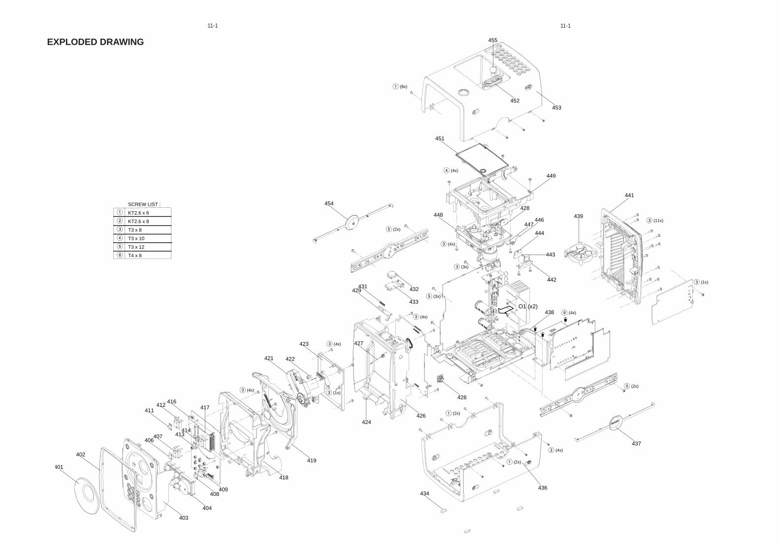
11-1 11-1
EXPLODED DRAWING
O1 (x2)
401
402
403
404
408409
406407
411412
413414
416417
418
419
424
421 422
423
426
427
429431
428
433
432
436434
442
443
447446
428448
449
451
444
453
438
454
437
441
452
455
4393 (11x)
3 (1x)
3 (4x)
5 (2x)
5 (2x)
1 (2x)
1 (2x)
6 (4x)
3 (3x)
5 (3x)
3 (4x)
3 (4x)
3 (4x)
1 (8x)
2 (4x)
4 (4x)
SCREW LIST :
KT2.6 x 6
KT2.6 x 8
T3 x 8
T3 x 10
T3 x 12
T4 x 8
1
2
3
4
5
6
3 (1x)

11-2 11-2
MECHANICAL & ACCESSORIES PARTSLIST
401 9965 000 20194 CD DOOR LENS 9965 000 20195 IFU MCV320402 9965 000 18185 CD CHROME RING 9965 000 11157 FM ANTENNA WIRE402 9965 000 20183 CD DOOR PANEL 4822 303 50082 AM LOOP ANTENNA404 9965 000 20182 KEY SET FUNCTION 9965 000 20196 SPK BOX MC-V320 20W406 9965 000 20187 KEY DISPLAY CAP 9965 000 20197 REMOTE CONTROL
407 9965 000 18203 KEY DISPLAY BKT 9965 000 18224 FFC 9P L=250MM P=1.25408 9965 000 20189 KEY REC CAP 9965 000 18225 FFC 13P L=200MM P=1.25409 9965 000 18205 KEY REC BKT 9965 000 18226 FFC P=1.0 L=115MM411 9965 000 20186 KEY POWER CAP 9965 000 18227 FFC 22P L=90MM P=1.0412 9965 000 18202 KEY POWER BKT 9965 000 18228 FFC 30P L=150MM P=1.25
413 9965 000 20188 KEY IR CAP 9965 000 20198 CORD PIN 1PY 1.5M414 9965 000 18204 KEY IR BKT416 9965 000 18255 REFLECT LIGHT GUIDE417 9965 000 18256 LCD LIGHT GUIDE418 9965 000 20180 CD DOOR
419 9965 000 20184 CD TRAY421 9965 000 18220 CD DECK DA23Z422 9965 000 18212 DMPR MECHA (SP)423 9965 000 20185 CD TRAY COVER424 9965 000 18213 CD DOOR SHAFT
426 9965 000 20179 CD BKT427 9965 000 18216 CD TRAY SPRING428 4822 529 10322 DAMPER ASSY429 9965 000 18198 CD DOOR LEVER431 9965 000 18214 CD DOOR LEVER SPRING
432 9965 000 20190 CD DOOR KNOB CAP433 9965 000 18206 CD DOOR KNOB BKT434 9965 000 18208 FOOT RUBBER436 9965 000 20176 CAB BOTTOM437 9965 000 20192 BRAND RIM RIGHT
438 9965 000 18223 AC CORD E 1750MM439 9965 000 19713 DC FAN441 9965 000 20177 CAB REAR442 9965 000 18181 BRACKET-LEFT443 9965 000 18211 SPRING-C LOCK
Note: Only these parts mentioned in the list are normal444 9965 000 18192 PUSH CATCH LEFT normal service parts.446 9965 000 18215 CASS DOOR SPRING447 9965 000 18207 CASS SPRING BKT448 9965 000 18221 CASSETT DECK CRM4304449 9965 000 19701 CASS BKT
451 9965 000 19700 CASS DOOR452 9965 000 20193 DECORATION TOP453 9965 000 20178 CAB TOP454 9965 000 20191 BRAND RIM LEFT455 9965 000 20181 KEY VOL MIC