BJT BIASING
in active region aF

transistor utilization as amplifier (CE)
in active region (aF), the transistor operates around a dc operating point (OP)
Necessity for dc transistor biasing
VPS – dc supply
VI – sets the OP: (VO, IO)
vi – input voltage
(to be amplified)
vo – output voltage
(amplified voltage)
• superposition of the
variable signal over the
dc regime
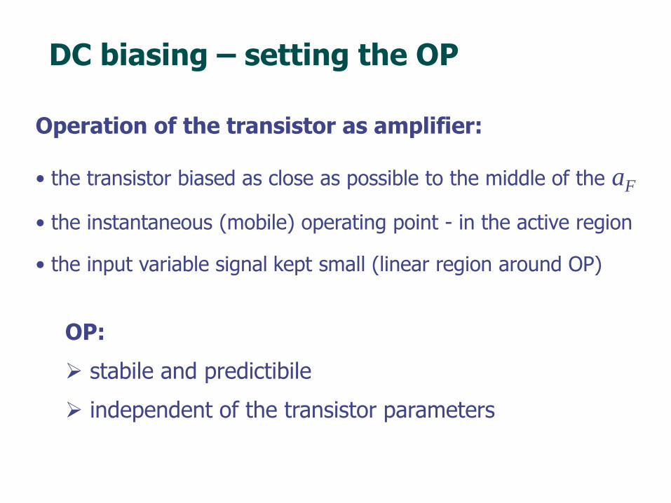
DC biasing – setting the OP
Operation of the transistor as amplifier:
• the transistor biased as close as possible to the middle of the aF
• the instantaneous (mobile) operating point - in the active region
• the input variable signal kept small (linear region around OP)
OP:
stabile and predictibile
independent of the transistor parameters

BJT biasing, unipolar (single) supply usual approach in discrete circuits
oppositely to MOSFET, for BJT appears:
- base current IB different from zero
- through collector and emitter do not flow exactly same current
CBBCEIIIII
1)1(
ECII One can approximate
BCII
• precise calculation: make use of IB
• approximate calculation: neglects IB
compared to the current through the
resistive voltage divider in the base of
the transistor
),(Q CCE IV
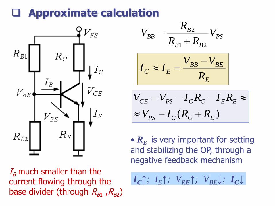
Approximate calculation
IB much smaller than the current flowing through the base divider (through RB1 ,RB2)
PS
BB
BBB V
RR
RV
21
2
E
BEBBEC
R
VVII
)( ECCPS
EECCPSCE
RRIV
RIRIVV
• RE is very important for setting
and stabilizing the OP, through a negative feedback mechanism
IC↑; IE↑; VRE↑; VBE↓; IC↓
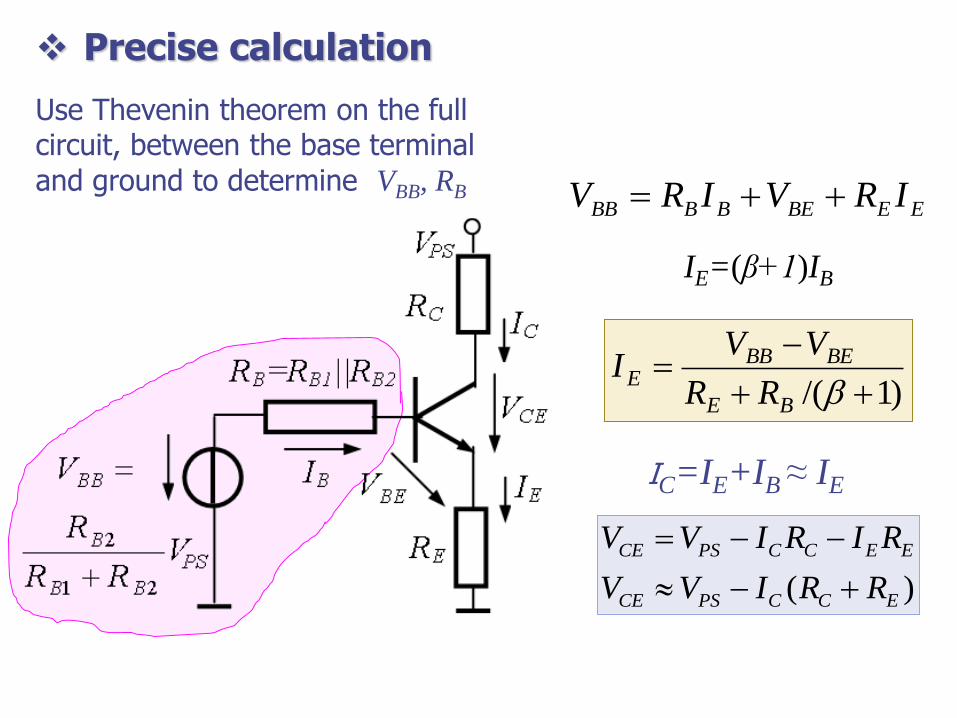
Use Thevenin theorem on the full circuit, between the base terminal
and ground to determine VBB, RB
IC=IE+IB ≈ IE
( )
CE PS C C E E
CE PS C C E
V V I R I R
V V I R R
)1/(
BE
BEBBE
RR
VVI
IE=(β+1)IB
EEBEBBBB IRVIRV
Precise calculation

Precise calculation
Stability analysis
• IE insensitive to β variations
)1(
B
E
RR
B
E
RR 10
•RB1, RB2 small values for the
independence of OP on β
•RB1, RB2 high values for the high
input resistance of the future
amplifier
• IE insensitive to temperature variations due to VBE
V1.0BBV
a ΔVBE variation of 0.1V can be neglected
vis a vis a VBB=3…5V
)1/(
BE
BEBBE
RR
VVI
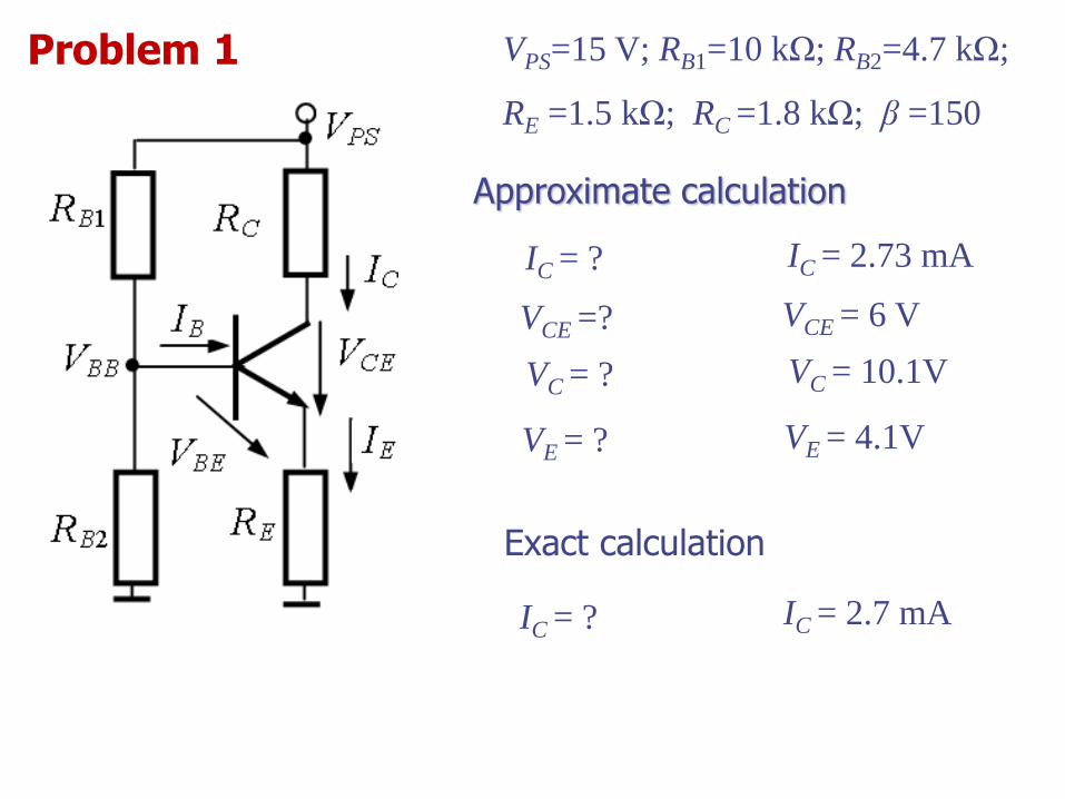
VPS=15 V; RB1=10 kΩ; RB2=4.7 kΩ;
RE =1.5 kΩ; RC =1.8 kΩ; β =150
Approximate calculation
Exact calculation
IC = ?
VCE =?
VC = ?
VE = ?
IC = 2.73 mA
VCE = 6 V
VC = 10.1V
VE = 4.1V
IC = ? IC = 2.7 mA
Problem 1
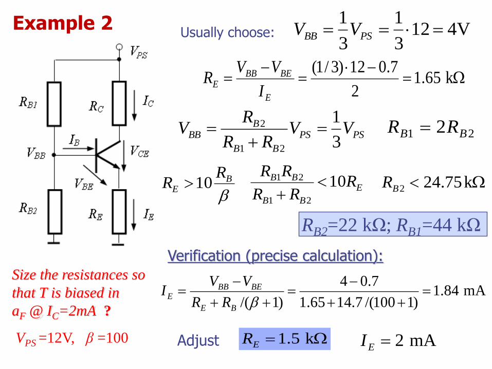
Example 2
Size the resistances so
that T is biased in
aF @ IC=2mA ?
VPS =12V, β =100
Usually choose: V4123
1
3
1 PSBB VV
k65.12
7.012)3/1(
E
BEBBE
I
VVR
PSPS
BB
BBB VV
RR
RV
3
1
21
2
21 2 BB RR
mA84.1)1100/(7.1465.1
7.04
)1/(
BE
BEBBE
RR
VVI
Verification (precise calculation):
RB2=22 kΩ; RB1=44 kΩ
B
E
RR 10 E
BB
BB RRR
RR10
21
21
k75.242BR
Adjust k5.1ER mA2EI
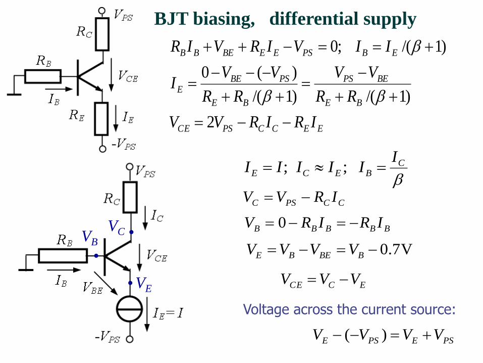
BJT biasing, differential supply
Voltage across the current source:
VE
VB
VC
C
BECE
IIIIII ;;
CCPSC IRVV
BBBBB IRIRV 0
V7.0 BBEBE VVVV
ECCE VVV
PSEPSE VVVV )(
EECCPSCE
BE
BEPS
BE
PSBEE
EBPSEEBEBB
IRIRVV
RR
VV
RR
VVI
IIVIRVIR
2
)1/()1/(
)(0
)1/(;0
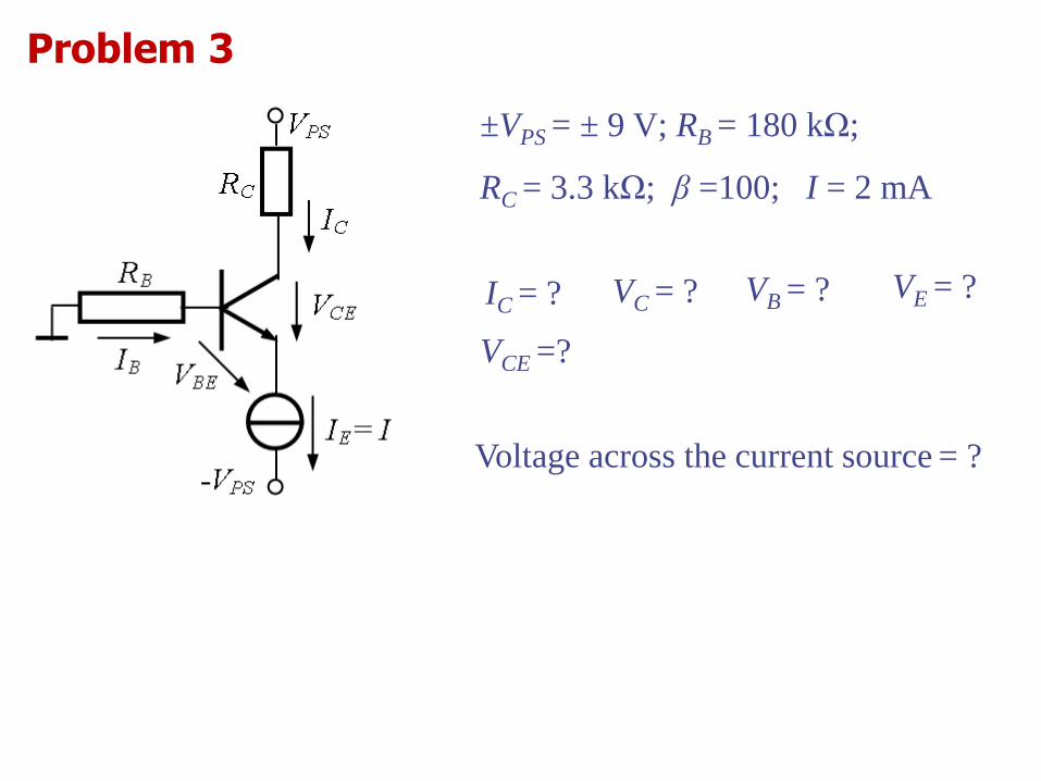
Problem 3
±VPS = ± 9 V; RB = 180 kΩ;
RC = 3.3 kΩ; β =100; I = 2 mA
IC = ?
VCE =?
VC = ? VE = ?VB = ?
Voltage across the current source = ?