Materials & Devices of Future: Challenges associated with Trends
SHRIRAM INSTITUTE FOR INDUSTRIAL RESEARCH19, UNVERSITY ROAD, DELHI - 110 007
Presented By :
Dr. R. K. Khandal

Outline
Materials & Devices: Attributes
Trends in Materials & Devices
Challenges associated with Major Sectors
Energy
Defense
Health
Infrastructure

Materials & Devices: Attributes
Past
Steadiness
Present Future
Productivity
Bulk
Quality
Controls
Surface
Precision
Software driven
Carbon footprint
Strength : weight
Emphasis on life- cycle
Environment friendly
Precision
Selective
Capacity driven
Inclusive
Capability driven
Innovation
Nano
Sensitive & Smart

Materials & Devices: Trends
Materials Devices
Devices
Trends
Applications
Materials
Purpose- SpecificSustainable
SafeEnergy-Efficient
Raw materials
GreenCradle-to-grave cycleEnvironment-friendly
AlternativesRenewable
Trends drive the advent of new materials and new devices in different industry sectors

ENERGY SECTOR
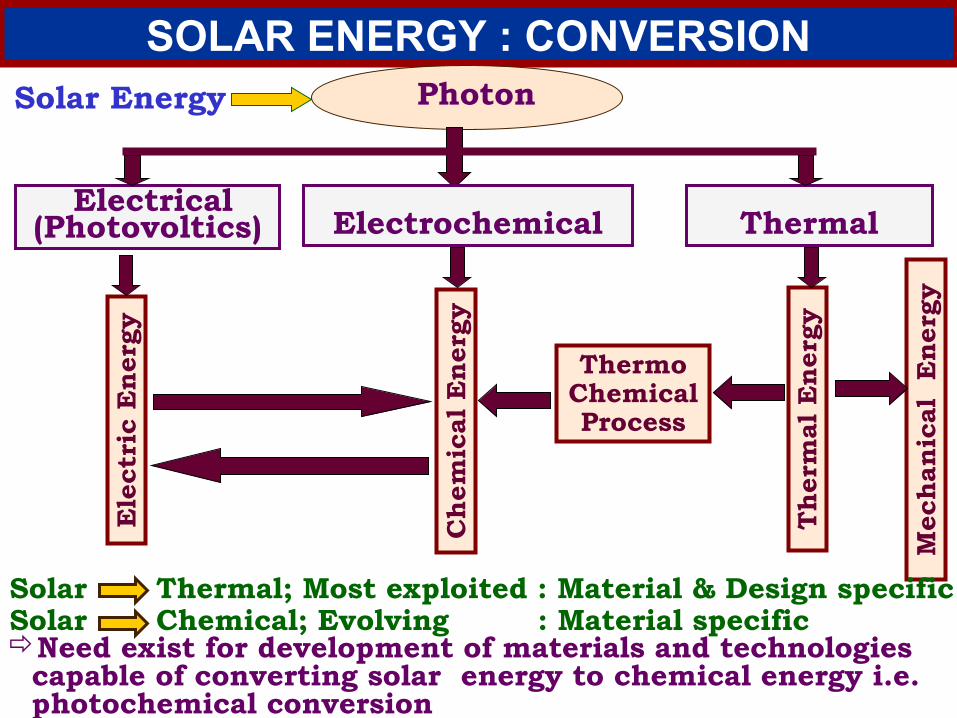
SOLAR ENERGY : CONVERSIONSolar Energy
Electrical (Photovoltics) Thermal
Ele
ctri
c E
ner
gy
Th
erm
al E
ner
gy
Thermo Chemical Process
Ch
emic
al E
ner
gy
Mec
han
ical
E
nerg
y
Photon
Solar Thermal; Most exploited : Material & Design specific Solar Chemical; Evolving : Material specific
Electrochemical
Need exist for development of materials and technologies capable of converting solar energy to chemical energy i.e. photochemical conversion

PHOTOCHEMICAL CONVERSIONThe Energy E of single photon is given by the Planck equation:- E=hν= hc/ λ
Sun light
.
…….. ...………………………………electron
Excitation photon
excited state
Non-radiative relaxation
Conduction band
Valence band
h+
e-
Band gap
E=hν
Every photochemical conversion process requires as an initial step, the absorption of photon energy and formation of the first excited state of the molecule
φ =Number of events
Number of photons absorbed

Solar Selectivity : Materials Response Frequency (Hz)
Visib
le
Infrare d
Ultravi olet
X-rays
Cosm
ic rays
1081010101210141016101810201022
Rad
iof requ
ency
Gam
ma rays
Microw
ave
High Potential for harnessing the solar energy
Processes involved Inner
electronic transition
Outer electronic transition
Molecular Vibrations
Molecular rotations vibrations
Electron spin resonance
Nuclear magnetic resonance
Change at atomic & molecular levels can become the via media for harnessing solar energy.
Solar sensitive materials undergo region specific transition Solar energy conversion

Energy Efficient Materials
Devices like smart windows can be designed by thin film coatings to create energy efficient buildings
Criteria Requirement Design Materials
Admit light,
reject solar heat
Transmit: 400 to 700nmReflect: 700 to >2500nm
Solar heating
Radiativecooling
Transmit /absorb: <2500nm
Reflect : >2500nm
Emit : >5000nm
TiO2 Bi2O3 Zn/ Cu, Ag,
Au/TiO2 Bi2O3
Al2O3 / MO/
Al2O3
SiO2;oxynitrides
Dielectric/ Metal/
Dielectric layer
Cermet Coating
Oxides
Semiconductor

DEFENSE SECTOR

CAMOUFLAGE : MATERIALS
Scattering Au, Ag, Pd, Ir, Ti Coloration is size dependent, Small
sized particles reflect light chromatically
Interference Metals, Interference Metal oxides between light
reflected from opposite parallel slides
Electronic Carbon Color is due to transition Black electronic transition
MATERIALS PROPERTIES
Selection of dispersing matrix for achieving coloration is the key !

Stealth Application: Metamaterials
η =√ µrε r
Metamaterials are engineered to have EM responses which are impossible in naturally occurring materials
1
2
1
2
+ve R.I.
-ve R.I.
Refractive Index
η =√ µrε r
µr: Permeability to magnetic field ε r: Permeability to electric field
µr or ε r= - ve
Induced phenomena
µr, ε r= +ve Natural phenomena

Materials for Stealth Applications: Composites
Periodic arrangement of R.I. variation controls movement of photons New energy levels within the band gaps can be created by breaking the
periodicity of the photonic material by enlarging, reducing or removing voids; the desired change in refractive index can be achieved by modifying the voids
Wavelength selective structures can be formed by careful selection of symmetry & spacing
Modification of light propagation takes place through enlarging, reducing or removing voids; optical cross-connects, switches & waveguides
Photonic band gap: Restricts transmission of light to defined set of bands
Voids
Enlarged voids Reduced voids Voids removal
Matrix

HEALTH SECTOR

Health Sector : Drug Delivery
Nanospheres Nanocapsules
Dendrimers
(Vesicular system)(Matrix system)
SLN particles(Solid lipid nanoparticles)
(Macromolecule, comprising of series of branches around an inner core)
Liposomes(Artificial spherical vesicles produced from natural phospholipids & cholestrol)
Polymeric micelles(Amphiphilic block copolymers which self-associate in aqueous solution)

INFRASTRUCTURE SECTOR

Infrastructure Sector : Paints & Coatings
Nanoparticles
Nanoparticles fill the voids created by larger particles in order to prevent water penetration & seal out moisture in the area of water proof coatings
Use of nanotechnology enhances Scratch& Abrasion resistance
UV-Protection
Mechanical properties

Infrastructure Sector : Smart Materials
On exposure to inputs, some materials exhibit change Utilization of such materials is key for green buildings
Thermochromic
Material InputHeat
Electrochromic
Photochromic Radiation (light)
Output
Colour
Electroluminescent Electric potential
Solar Radiation
Heat
LightPhotoluminescent
Thermoluminescent
Piezoelectric Mechanical Force
Heat
Electric potentialShapePyroelectric
Electrostrictive
Magnetostrictive Magnetic potential
Electric Potential

THANK YOU