


Scholars' Mine Scholars' Mine
Doctoral Dissertations Student Theses and Dissertations
Fall 2018
Advanced topologies of high-voltage-gain DC-DC boost Advanced topologies of high-voltage-gain DC-DC boost
converters for renewable energy applications converters for renewable energy applications
Ahmad Alzahrani
Follow this and additional works at: https://scholarsmine.mst.edu/doctoral_dissertations
Part of the Electrical and Computer Engineering Commons
Department: Electrical and Computer Engineering Department: Electrical and Computer Engineering
Recommended Citation Recommended Citation Alzahrani, Ahmad, "Advanced topologies of high-voltage-gain DC-DC boost converters for renewable energy applications" (2018). Doctoral Dissertations. 2716. https://scholarsmine.mst.edu/doctoral_dissertations/2716
This thesis is brought to you by Scholars' Mine, a service of the Missouri S&T Library and Learning Resources. This work is protected by U. S. Copyright Law. Unauthorized use including reproduction for redistribution requires the permission of the copyright holder. For more information, please contact [email protected].
ADVANCED TOPOLOGIES OF HIGH-VOLTAGE-GAIN DC-DC BOOST
CONVERTERS FOR RENEWABLE ENERGY APPLICATIONS
by
AHMAD SAEED Y. ALZAHRANI
A DISSERTATION
Presented to the Graduate Faculty of the
MISSOURI UNIVERSITY OF SCIENCE AND TECHNOLOGY
In Partial Fulfillment of the Requirements for the Degree
DOCTOR OF PHILOSOPHY
in
ELECTRICAL ENGINEERING
2018
Approved by
Mehdi Ferdowsi, AdvisorJonathan KimballPourya ShamsiDonald WunschAli Rownaghi

Copyright 2018
AHMAD SAEED Y. ALZAHRANI
All Rights Reserved
iii
PUBLICATION DISSERTATION OPTION
This dissertation consists of the following four articles which have been submitted
for publication, or will be submitted for publication as follows:
Paper I: Pages 14-51 are submitted to IEEE ACCESS.
Paper II: Pages 52-85 are submitted IEEE transactions on Power Electronics.
Paper III: Pages 86-119 are submitted to IEEE Journal of Emerging and
Selected Topics in Power Electronics.
Paper IV: Pages 120-143 are submitted to IEEE Transactions on Industrial
Electronics
iv
ABSTRACT
This dissertation proposes several advanced power electronic converters that are
suitable for integrating low-voltage dc input sources, such as photovoltaic (PV) solar panels,
to a high voltage dc bus in a 200 − 960 V dc distribution system. The proposed converters
operate in the continuous conduction mode (CCM) and offer desirable features such as low-
voltage stresses on components, continuous input currents, and the ability to integrate several
independent dc input sources. First, a family of scalable interleaved boost converters with
voltage multiplier cells (VMC) is introduced. Several possible combinations of Dickson
and Cockcroft-Walton VMCs are demonstrated and compared in terms of the voltage gain,
number of components, and input current sharing. This dissertation also presents a novel
VMCstructure calledBi-foldDickson. The novelVMCoffers equal current sharing between
phases regardless of the number of stages, voltage ripple cancellation at each stage, and
does not require an output diode. A family of high-voltage-gain multilevel boost converters
is presented, with detailed example of the hybrid flyback and three-level boost converter.
In this family, the effective frequency seen by the magnetic element is multiple times
the switching frequency, and therefore smaller magnetic devices can be used. Theory of
operations, steady-state analysis, component selections, simulation, and efficiency analysis
are included for each proposed converter. The operation of the proposed converters was
further verified with 80 − 200 W hardware prototypes.

v
ACKNOWLEDGMENTS
I would like to express my deepest and sincerest gratitude to my advisor, Dr. Mehdi
Ferdowsi for his outstanding guidance, leadership, understanding and patience throughout
my Ph.D. research, without him this dissertation would not have been completed. His vivid
demonstrations of power electronics and professional guidance helped me to come up with
ideas and organize my thoughts.
I would like to thank to Dr. Pourya Shamsi, Dr. Donald Wunsch, Dr. Ali Rownaghi
and Dr. Jonathan Kimball for their invaluable support, academic guidance and for kindly
agreeing to be on my committee. I would like to thank Dr. Kimball for tips and tricks he
taught me about PCBs and giving me the opportunity to mentor NSF REU students.
I would like to thank my colleagues and lab mates and Md. Rashidulzzaman, Tamal
Paul and Haidar Almubarak for helping me during my research time. Special thanks to the
ECE front office Carol, Jony, and Erin for helping me. I would like also to thank staff of the
graduate studies and the library for providing me with advices and assistance.
I would like to thank Najran University, Saudi Arabian Cultural Mission, and Min-
istry of Education in Saudi Arabia for the opportunity to pursue my graduate degrees and
for the support.
Finally, I am indebted to my family for their unconditional love and support through-
out all aspects of my life.

vi
TABLE OF CONTENTS
Page
PUBLICATION DISSERTATION OPTION . . . . . . . . . . . . . . . . . . . . . . . . . . . . . . . . . . . . . . iii
ABSTRACT . . . . . . . . . . . . . . . . . . . . . . . . . . . . . . . . . . . . . . . . . . . . . . . . . . . . . . . . . . . . . . . . . . iv
ACKNOWLEDGMENTS . . . . . . . . . . . . . . . . . . . . . . . . . . . . . . . . . . . . . . . . . . . . . . . . . . . . . . v
LIST OF ILLUSTRATIONS . . . . . . . . . . . . . . . . . . . . . . . . . . . . . . . . . . . . . . . . . . . . . . . . . . . . xi
LIST OF TABLES . . . . . . . . . . . . . . . . . . . . . . . . . . . . . . . . . . . . . . . . . . . . . . . . . . . . . . . . . . . . . xvii
SECTION
1. INTRODUCTION. . . . . . . . . . . . . . . . . . . . . . . . . . . . . . . . . . . . . . . . . . . . . . . . . . . . . . . . . . 1
1.1. OVERVIEW .. . . . . . . . . . . . . . . . . . . . . . . . . . . . . . . . . . . . . . . . . . . . . . . . . . . . . . . . . . . . . . . . . . . . . 1
1.2. LITERATURE REVIEW .. . . . . . . . . . . . . . . . . . . . . . . . . . . . . . . . . . . . . . . . . . . . . . . . . . . . . . . 3
1.2.1. Conventional Boost Converter . . . . . . . . . . . . . . . . . . . . . . . . . . . . . . . . . . . . . . . . . . 3
1.2.2. Cascaded and Stacked Boost Converters . . . . . . . . . . . . . . . . . . . . . . . . . . . . . . . 4
1.2.3. Three-level Boost Converter . . . . . . . . . . . . . . . . . . . . . . . . . . . . . . . . . . . . . . . . . . . . 7
1.2.4. Isolated Converters . . . . . . . . . . . . . . . . . . . . . . . . . . . . . . . . . . . . . . . . . . . . . . . . . . . . . . 8
1.2.5. Switched Capacitors and Hybrid Boost Converters. . . . . . . . . . . . . . . . . . . . 9
1.2.6. Interleaved Boost Converters . . . . . . . . . . . . . . . . . . . . . . . . . . . . . . . . . . . . . . . . . . . 10
1.3. RESEARCH CONTRIBUTION . . . . . . . . . . . . . . . . . . . . . . . . . . . . . . . . . . . . . . . . . . . . . . . . 12
PAPER
I. A FAMILY OF NON-ISOLATED INTERLEAVED BOOST CONVERTERSWITH VOLTAGE MULTIPLIER CELLS. . . . . . . . . . . . . . . . . . . . . . . . . . . . . . . . . . . . . 14
vii
ABSTRACT . . . . . . . . . . . . . . . . . . . . . . . . . . . . . . . . . . . . . . . . . . . . . . . . . . . . . . . . . . . . . . . . . . . . . . . . . . . . 14
1. INTRODUCTION . . . . . . . . . . . . . . . . . . . . . . . . . . . . . . . . . . . . . . . . . . . . . . . . . . . . . . . . . . . . . . . 15
2. THEORY OF OPERATION AND GENERAL STRUCTURE OF THEPROPOSED FAMILY . . . . . . . . . . . . . . . . . . . . . . . . . . . . . . . . . . . . . . . . . . . . . . . . . . . . . . . . . . . 17
2.1. INTERLEAVED BOOST STAGE . . . . . . . . . . . . . . . . . . . . . . . . . . . . . . . . . . . . . . 18
2.2. VOLTAGE MULTIPLIER STAGE . . . . . . . . . . . . . . . . . . . . . . . . . . . . . . . . . . . . . 23
2.3. TOPOLOGIES OF A TWO-PHASE INTERLEAVED BOOSTCONVERTER WITH VMCS . . . . . . . . . . . . . . . . . . . . . . . . . . . . . . . . . . . . . . . . . . 27
2.4. POSSIBLE MODIFICATIONS TO THE TOPOLOGIES . . . . . . . . . . . . 28
2.4.1. Convert a Floating Output Converter to Grounded Output . 28
2.4.2. Modification to Make the Converter Isolated . . . . . . . . . . . . . . . 29
2.4.3. Connecting Two Different VMCs to Obtain the OverallNonuniform Converter . . . . . . . . . . . . . . . . . . . . . . . . . . . . . . . . . . . . . . . 30
3. MODES OF OPERATION AND STEADY-STATE ANALYSIS OF ANEXAMPLE CONVERTER . . . . . . . . . . . . . . . . . . . . . . . . . . . . . . . . . . . . . . . . . . . . . . . . . . . . . 30
3.1. MODE 1: BOTH MOSFETS ARE ON . . . . . . . . . . . . . . . . . . . . . . . . . . . . . . . . 31
3.2. MODE 2: S1 IS ON AND S2 IS OFF . . . . . . . . . . . . . . . . . . . . . . . . . . . . . . . . . . 33
3.3. MODE 3: S1 IS OFF AND S2 IS ON . . . . . . . . . . . . . . . . . . . . . . . . . . . . . . . . . . 33
3.4. STEADY-STATE VOLTAGE GAIN . . . . . . . . . . . . . . . . . . . . . . . . . . . . . . . . . . . 33
4. COMPONENT SELECTIONS AND EFFICIENCY ANALYSIS . . . . . . . . . . . . 34
4.1. INDUCTOR SELECTION . . . . . . . . . . . . . . . . . . . . . . . . . . . . . . . . . . . . . . . . . . . . . 36
4.2. ACTIVE SWITCHES SELECTION . . . . . . . . . . . . . . . . . . . . . . . . . . . . . . . . . . . 37
4.3. DIODE SELECTION . . . . . . . . . . . . . . . . . . . . . . . . . . . . . . . . . . . . . . . . . . . . . . . . . . . 37
4.4. CAPACITOR SELECTION. . . . . . . . . . . . . . . . . . . . . . . . . . . . . . . . . . . . . . . . . . . . . 38
5. POWER LOSSES AND EFFICIENCY ANALYSIS . . . . . . . . . . . . . . . . . . . . . . . . . . . 38
6. SIMULATION . . . . . . . . . . . . . . . . . . . . . . . . . . . . . . . . . . . . . . . . . . . . . . . . . . . . . . . . . . . . . . . . . . . 40
7. EXPERIMENTAL IMPLEMENTATION AND RESULTS . . . . . . . . . . . . . . . . . . . 40
8. CONCLUSION . . . . . . . . . . . . . . . . . . . . . . . . . . . . . . . . . . . . . . . . . . . . . . . . . . . . . . . . . . . . . . . . . . 47
viii
REFERENCES . . . . . . . . . . . . . . . . . . . . . . . . . . . . . . . . . . . . . . . . . . . . . . . . . . . . . . . . . . . . . . . . . . . . . . . . . 47
II. HIGH-VOLTAGE-GAIN DC-DC STEP-UP CONVERTER WITH BI-FOLDDICKSON VOLTAGE MULTIPLIER CELLS . . . . . . . . . . . . . . . . . . . . . . . . . . . . . . . . 52
ABSTRACT . . . . . . . . . . . . . . . . . . . . . . . . . . . . . . . . . . . . . . . . . . . . . . . . . . . . . . . . . . . . . . . . . . . . . . . . . . . . 52
1. INTRODUCTION . . . . . . . . . . . . . . . . . . . . . . . . . . . . . . . . . . . . . . . . . . . . . . . . . . . . . . . . . . . . . . . 53
2. CONSTRUCTION OF BI-FOLD DICKSON SC/VMCS. . . . . . . . . . . . . . . . . . . . . . 57
3. THE PROPOSED TOPOLOGY INTRODUCTION AND THEORY OFOPERATION. . . . . . . . . . . . . . . . . . . . . . . . . . . . . . . . . . . . . . . . . . . . . . . . . . . . . . . . . . . . . . . . . . . . . 58
4. MODE ANALYSIS AND STEADY STATE VOLTAGE GAIN. . . . . . . . . . . . . . . 59
4.1. MODE 1 (T0 − T1) AND (T2 − T3) : BOTH Q1 AND Q2 ARE ON . . 59
4.2. MODE 2 (T1 − T2): Q1 IS ON AND Q2 IS OFF . . . . . . . . . . . . . . . . . . . . . . 59
4.3. MODE 3 (T3 − T4) : Q1 IS OFF AND Q2 IS ON . . . . . . . . . . . . . . . . . . . . . . 62
5. DISCONTINOUS CONDUCTION MODE AND BOUNDARY CON-DUCTION MODE . . . . . . . . . . . . . . . . . . . . . . . . . . . . . . . . . . . . . . . . . . . . . . . . . . . . . . . . . . . . . . . 66
5.1. DCM OPERATION . . . . . . . . . . . . . . . . . . . . . . . . . . . . . . . . . . . . . . . . . . . . . . . . . . . . 66
5.1.1. Mode 1 . . . . . . . . . . . . . . . . . . . . . . . . . . . . . . . . . . . . . . . . . . . . . . . . . . . . . . . . 67
5.1.2. Mode 2 . . . . . . . . . . . . . . . . . . . . . . . . . . . . . . . . . . . . . . . . . . . . . . . . . . . . . . . . 67
5.1.3. Mode 3 . . . . . . . . . . . . . . . . . . . . . . . . . . . . . . . . . . . . . . . . . . . . . . . . . . . . . . . . 67
5.1.4. Mode 4 . . . . . . . . . . . . . . . . . . . . . . . . . . . . . . . . . . . . . . . . . . . . . . . . . . . . . . . . 67
5.1.5. Mode 5 . . . . . . . . . . . . . . . . . . . . . . . . . . . . . . . . . . . . . . . . . . . . . . . . . . . . . . . . 67
5.1.6. Steady-state Analysis . . . . . . . . . . . . . . . . . . . . . . . . . . . . . . . . . . . . . . . . . 68
5.2. BOUNDARY CONDUCTION MODE (BCM) . . . . . . . . . . . . . . . . . . . . . . . . 69
6. COMPONENTS SELECTION AND EFFICIENCY CALCULATIONS. . . . . 70
6.1. INDUCTOR SELECTION . . . . . . . . . . . . . . . . . . . . . . . . . . . . . . . . . . . . . . . . . . . . . 70
6.2. ACTIVE SWITCH SELECTION. . . . . . . . . . . . . . . . . . . . . . . . . . . . . . . . . . . . . . . 71
6.3. DIODE SELECTION . . . . . . . . . . . . . . . . . . . . . . . . . . . . . . . . . . . . . . . . . . . . . . . . . . . 72
6.4. CAPACITORS SELECTION . . . . . . . . . . . . . . . . . . . . . . . . . . . . . . . . . . . . . . . . . . . 73

ix
6.5. EFFICIENCY ANALYSIS. . . . . . . . . . . . . . . . . . . . . . . . . . . . . . . . . . . . . . . . . . . . . . 73
7. SIMULATION . . . . . . . . . . . . . . . . . . . . . . . . . . . . . . . . . . . . . . . . . . . . . . . . . . . . . . . . . . . . . . . . . . . 75
8. EXPERIMENTAL IMPLEMENTATION AND RESULTS . . . . . . . . . . . . . . . . . . . 77
9. CONCLUSION . . . . . . . . . . . . . . . . . . . . . . . . . . . . . . . . . . . . . . . . . . . . . . . . . . . . . . . . . . . . . . . . . . 82
REFERENCES . . . . . . . . . . . . . . . . . . . . . . . . . . . . . . . . . . . . . . . . . . . . . . . . . . . . . . . . . . . . . . . . . . . . . . . . . 82
III. A FAMILY OF HIGH-VOLTAGE-GAIN MULTILEVEL BOOST CONVERT-ERS . . . . . . . . . . . . . . . . . . . . . . . . . . . . . . . . . . . . . . . . . . . . . . . . . . . . . . . . . . . . . . . . . . . . . . 86
ABSTRACT . . . . . . . . . . . . . . . . . . . . . . . . . . . . . . . . . . . . . . . . . . . . . . . . . . . . . . . . . . . . . . . . . . . . . . . . . . . . 86
1. INTRODUCTION . . . . . . . . . . . . . . . . . . . . . . . . . . . . . . . . . . . . . . . . . . . . . . . . . . . . . . . . . . . . . . . 87
2. PROPOSED FAMILY OFMULTILEVEL BOOST CONVERTERWITHHIGH GAIN . . . . . . . . . . . . . . . . . . . . . . . . . . . . . . . . . . . . . . . . . . . . . . . . . . . . . . . . . . . . . . . . . . . . . . 89
2.1. INTERLEAVING . . . . . . . . . . . . . . . . . . . . . . . . . . . . . . . . . . . . . . . . . . . . . . . . . . . . . . . 89
2.2. HIGH GAIN CELLS . . . . . . . . . . . . . . . . . . . . . . . . . . . . . . . . . . . . . . . . . . . . . . . . . . . . 91
3. EXAMPLE CONVERTER . . . . . . . . . . . . . . . . . . . . . . . . . . . . . . . . . . . . . . . . . . . . . . . . . . . . . . 95
3.1. THEORY OF OPERATION . . . . . . . . . . . . . . . . . . . . . . . . . . . . . . . . . . . . . . . . . . . . 95
4. COMPONENT SELECTIONS AND EFFICIENCY ANALYSIS . . . . . . . . . . . . 100
4.1. ACTIVE SWITCHES . . . . . . . . . . . . . . . . . . . . . . . . . . . . . . . . . . . . . . . . . . . . . . . . . . . 100
4.2. DIODES . . . . . . . . . . . . . . . . . . . . . . . . . . . . . . . . . . . . . . . . . . . . . . . . . . . . . . . . . . . . . . . . . 101
4.3. CAPACITORS . . . . . . . . . . . . . . . . . . . . . . . . . . . . . . . . . . . . . . . . . . . . . . . . . . . . . . . . . . . 101
4.4. COUPLED INDUCTORS . . . . . . . . . . . . . . . . . . . . . . . . . . . . . . . . . . . . . . . . . . . . . . 102
4.5. THE LOSS ANALYSIS . . . . . . . . . . . . . . . . . . . . . . . . . . . . . . . . . . . . . . . . . . . . . . . . . 102
5. SIMULATION . . . . . . . . . . . . . . . . . . . . . . . . . . . . . . . . . . . . . . . . . . . . . . . . . . . . . . . . . . . . . . . . . . . 103
5.1. PHOTOVOLTAIC SOURCE SIMULATION. . . . . . . . . . . . . . . . . . . . . . . . . . 106
5.2. MPPT CONTROL. . . . . . . . . . . . . . . . . . . . . . . . . . . . . . . . . . . . . . . . . . . . . . . . . . . . . . . 109
6. EXPERIMENTAL . . . . . . . . . . . . . . . . . . . . . . . . . . . . . . . . . . . . . . . . . . . . . . . . . . . . . . . . . . . . . . . 109
7. CONCLUSIONS . . . . . . . . . . . . . . . . . . . . . . . . . . . . . . . . . . . . . . . . . . . . . . . . . . . . . . . . . . . . . . . . . 110
REFERENCES . . . . . . . . . . . . . . . . . . . . . . . . . . . . . . . . . . . . . . . . . . . . . . . . . . . . . . . . . . . . . . . . . . . . . . . . . 115

x
IV. A FAMILY OF INTERLEAVED STEP-UP TOPOLOGIES USING SINGLE-SWITCH MULTISTAGE BOOST CONVERTERS AND VOLTAGE MULTI-PLIER CELLS . . . . . . . . . . . . . . . . . . . . . . . . . . . . . . . . . . . . . . . . . . . . . . . . . . . . . . . . . . . . . 120
ABSTRACT . . . . . . . . . . . . . . . . . . . . . . . . . . . . . . . . . . . . . . . . . . . . . . . . . . . . . . . . . . . . . . . . . . . . . . . . . . . . 120
1. INTRODUCTION . . . . . . . . . . . . . . . . . . . . . . . . . . . . . . . . . . . . . . . . . . . . . . . . . . . . . . . . . . . . . . . 121
2. THEORY OF OPERATION AND STEADY-STATE ANALYSIS . . . . . . . . . . . . 123
2.1. MODE 1: BOTH ACTIVE SWITCHES ARE ON . . . . . . . . . . . . . . . . . . . . 124
2.2. MODE 2: Q1 IS ON AND Q2 IS OFF . . . . . . . . . . . . . . . . . . . . . . . . . . . . . . . . . 129
2.3. MODE 3: Q1 IS OFF AND Q2 IS ON . . . . . . . . . . . . . . . . . . . . . . . . . . . . . . . . . 129
2.4. STEADY-STATE ANALYSIS AND STATIC VOLTAGE GAIN . . . . . 130
3. COMPONENTS SELECTION AND EFFICIENCY ANALYSIS . . . . . . . . . . . . 132
3.1. ACTIVE SWITCHES . . . . . . . . . . . . . . . . . . . . . . . . . . . . . . . . . . . . . . . . . . . . . . . . . . . 132
3.2. DIODES . . . . . . . . . . . . . . . . . . . . . . . . . . . . . . . . . . . . . . . . . . . . . . . . . . . . . . . . . . . . . . . . . 133
3.3. INDUCTORS. . . . . . . . . . . . . . . . . . . . . . . . . . . . . . . . . . . . . . . . . . . . . . . . . . . . . . . . . . . . 133
3.4. CAPACITORS . . . . . . . . . . . . . . . . . . . . . . . . . . . . . . . . . . . . . . . . . . . . . . . . . . . . . . . . . . . 135
3.5. EFFICIENCY ANALYSIS. . . . . . . . . . . . . . . . . . . . . . . . . . . . . . . . . . . . . . . . . . . . . . 135
4. EXPERIMENTAL IMPLEMENTATION AND RESULTS . . . . . . . . . . . . . . . . . . . 136
5. CONCLUSIONS . . . . . . . . . . . . . . . . . . . . . . . . . . . . . . . . . . . . . . . . . . . . . . . . . . . . . . . . . . . . . . . . . 140
REFERENCES . . . . . . . . . . . . . . . . . . . . . . . . . . . . . . . . . . . . . . . . . . . . . . . . . . . . . . . . . . . . . . . . . . . . . . . . . 140
SECTION
2. SUMMARY AND CONCLUSIONS . . . . . . . . . . . . . . . . . . . . . . . . . . . . . . . . . . . . . . . . . 144
REFERENCES . . . . . . . . . . . . . . . . . . . . . . . . . . . . . . . . . . . . . . . . . . . . . . . . . . . . . . . . . . . . . . . . 146
VITA . . . . . . . . . . . . . . . . . . . . . . . . . . . . . . . . . . . . . . . . . . . . . . . . . . . . . . . . . . . . . . . . . . . . . . . . . 157

xi
LIST OF ILLUSTRATIONS
Figure Page
SECTION
1.1. The conventional boost converter . . . . . . . . . . . . . . . . . . . . . . . . . . . . . . . . . . . . . . . . . . . . . . . . . . . 4
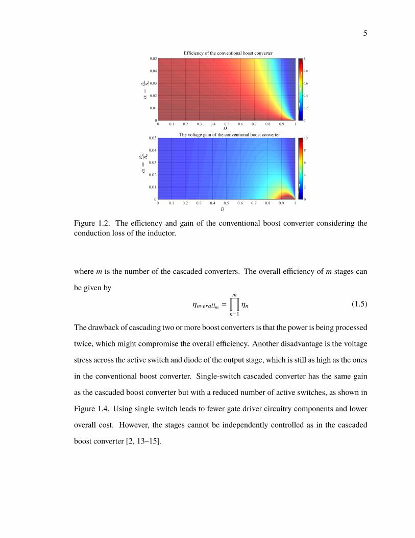
1.2. The efficiency and gain of the conventional boost converter considering theconduction loss of the inductor. . . . . . . . . . . . . . . . . . . . . . . . . . . . . . . . . . . . . . . . . . . . . . . . . . . . . . 5
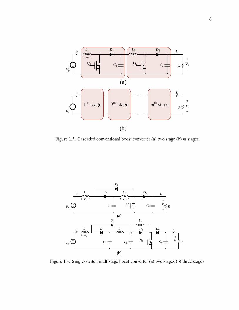
1.3. Cascaded conventional boost converter (a) two stage (b) m stages . . . . . . . . . . . . . . . . 6
1.4. Single-switch multistage boost converter (a) two stages (b) three stages . . . . . . . . . . 6
1.5. Stacked boost converter a) Quadratic b) Quartic . . . . . . . . . . . . . . . . . . . . . . . . . . . . . . . . . . . 7
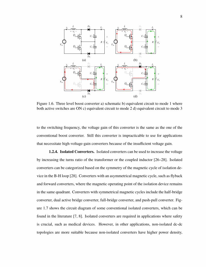
1.6. Three level boost converter a) schematic b) equivalent circuit to mode 1 whereboth active switches are ON c) equivalent circuit to mode 2 d) equivalentcircuit to mode 3 . . . . . . . . . . . . . . . . . . . . . . . . . . . . . . . . . . . . . . . . . . . . . . . . . . . . . . . . . . . . . . . . . . . . . 8
1.7. Examples of isolated Dc-dc topologies converter a) two-switch flyback con-verter b) two-switch forward converter c) Voltage-fed half-bridge converter d)dual active bridge converter e) Full-bridge converter. . . . . . . . . . . . . . . . . . . . . . . . . . . . . . . 9
1.8. Example of common switched capacitor circuits a) Cascaded voltage doublerb) Fibonacci SC c) Dickson SC d) Series parallel SC . . . . . . . . . . . . . . . . . . . . . . . . . . . . . . 10
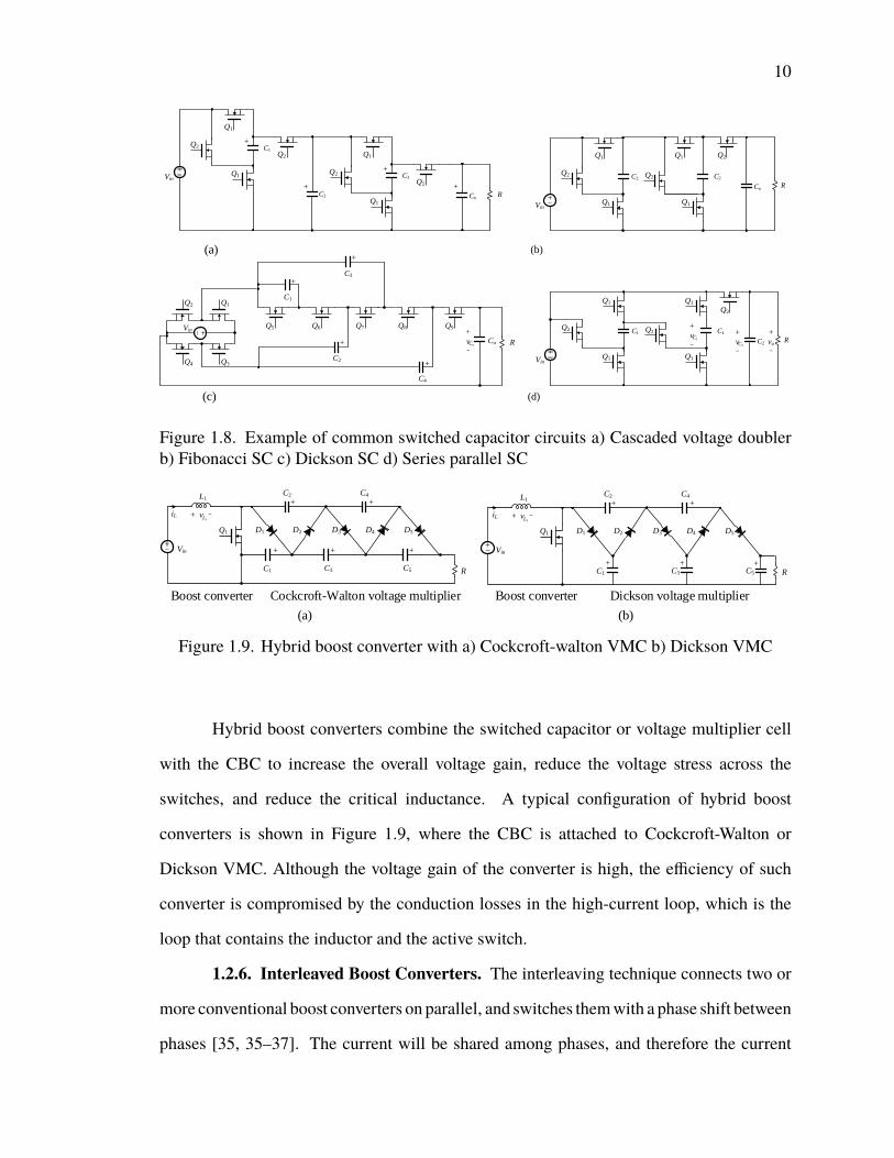
1.9. Hybrid boost converter with a) Cockcroft-walton VMC b) Dickson VMC . . . . . . . 10
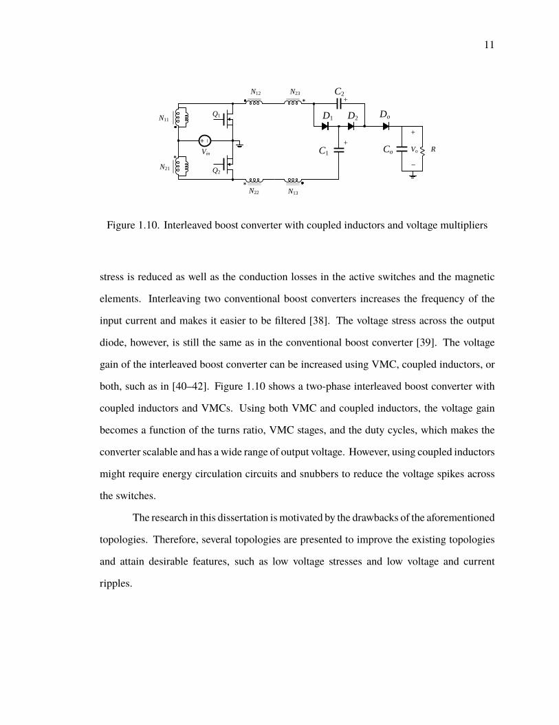
1.10. Interleaved boost converter with coupled inductors and voltage multipliers . . . . . . 11
PAPER I
1. General structure of the proposed family: (a) with output diode and capacitor(b) with LC filter output . . . . . . . . . . . . . . . . . . . . . . . . . . . . . . . . . . . . . . . . . . . . . . . . . . . . . . . . . . . . . 18
2. Reduction of energy storage at multiple phases. In case of two phases, therequired energy storage is reduced by 50%. . . . . . . . . . . . . . . . . . . . . . . . . . . . . . . . . . . . . . . . 19
3. The normalized current ripples with respect to a single phase boost converter. . . 21
4. Interleaved boost stage with output waveforms: (a) two phases (b) three phases. 21
5. The switching pattern for the two-phase interleaved boost converter. The activeswitches are driven by two out of phase signals, and the converter operates inthree modes of operation in the CCM. . . . . . . . . . . . . . . . . . . . . . . . . . . . . . . . . . . . . . . . . . . . . . . 22
xii
6. The switching pattern for a three-phase interleaved boost converter. Theconverter is driven by three signals with a phase shift of 120, and the converteroperates at four modes of operation in the CCM.. . . . . . . . . . . . . . . . . . . . . . . . . . . . . . . . . . . 22
7. Two main voltage multiplier cells: (a) Dickson VMC (b) Cockcroft-Walton VMC. 23
8. Various topologies belong to the interleaved boost converter with voltagemultiplier cells (group A-D). The output is filtered using an output diode anda capacitor filter. . . . . . . . . . . . . . . . . . . . . . . . . . . . . . . . . . . . . . . . . . . . . . . . . . . . . . . . . . . . . . . . . . . . . . . 24
9. Various topologies belong to the interleaved boost converter with voltagemultiplier cells (group E-H): with an output diode and a capacitor filter. . . . . . . . . . 25
10. Using an output LC filter instead of a diode-capacitor for the same groupsaforementioned. . . . . . . . . . . . . . . . . . . . . . . . . . . . . . . . . . . . . . . . . . . . . . . . . . . . . . . . . . . . . . . . . . . . . . . 26
11. Modification to convert a floating output converter to a grounded output converter. 28
12. Group A and F can be converted to have a grounded output. Both have anideal voltage gain of M = N+1
1−d , which is N1−d less than the ones with floating
outputs. . . . . . . . . . . . . . . . . . . . . . . . . . . . . . . . . . . . . . . . . . . . . . . . . . . . . . . . . . . . . . . . . . . . . . . . . . . . . . . . 29
13. The presented family can be modified by adding an isolation device to meetthe isolation requirement and improve the voltage gain. . . . . . . . . . . . . . . . . . . . . . . . . . . . 29
14. Example of nonuniform topologies. The converter features two different typesof VMCs, a cell from group F and Cockcroft-Walton VMC. . . . . . . . . . . . . . . . . . . . . . . 30
15. Example converter; an interleaved boost stage with a 3 level VMC . . . . . . . . . . . . . . . 32
16. Modes of operation of the example converter; (a) mode 1 (b) mode 2 (c) mode 3 32
17. The example converter can convert the voltage from two independent powersources. . . . . . . . . . . . . . . . . . . . . . . . . . . . . . . . . . . . . . . . . . . . . . . . . . . . . . . . . . . . . . . . . . . . . . . . . . . . . . . . 35
18. Simulation waveforms of voltages and currents across semiconductor switchesand inductors . . . . . . . . . . . . . . . . . . . . . . . . . . . . . . . . . . . . . . . . . . . . . . . . . . . . . . . . . . . . . . . . . . . . . . . . . 41
19. Simulation waveforms of the capacitors’ voltage and the output voltage in thesteady-state . . . . . . . . . . . . . . . . . . . . . . . . . . . . . . . . . . . . . . . . . . . . . . . . . . . . . . . . . . . . . . . . . . . . . . . . . . . 41
20. Simulation of the capacitors’ currents . . . . . . . . . . . . . . . . . . . . . . . . . . . . . . . . . . . . . . . . . . . . . . . 42
21. Simulation waveforms of the diodes’ currents . . . . . . . . . . . . . . . . . . . . . . . . . . . . . . . . . . . . . . 42
22. Efficiency analysis of the example converter; the actual losses (left) and theloss breakdown (right) . . . . . . . . . . . . . . . . . . . . . . . . . . . . . . . . . . . . . . . . . . . . . . . . . . . . . . . . . . . . . . . 43
23. The hardware prototype and the experimental setup . . . . . . . . . . . . . . . . . . . . . . . . . . . . . . . 44

xiii
24. Experimental results of the voltage across the active switches and the diodes . . . . 45
25. Experimental results of the voltage across the capacitors . . . . . . . . . . . . . . . . . . . . . . . . . . 45
26. Experimental results of the input current, inductor currents, active switchesand diode currents . . . . . . . . . . . . . . . . . . . . . . . . . . . . . . . . . . . . . . . . . . . . . . . . . . . . . . . . . . . . . . . . . . . . 46
27. Experimental results of the capacitors’ currents and the output current . . . . . . . . . . . 46
PAPER II
1. Application of a high-gain DC-DC converter . . . . . . . . . . . . . . . . . . . . . . . . . . . . . . . . . . . . . . . 55
2. The construction of a bi-fold Dickson cell. The BD cell is constructed usingtwo conventional Dickson cells, and one of the cells is rotated by 180. Then,they are connected so that a single VMC stage consists of two complementaryswitches and two capacitors. . . . . . . . . . . . . . . . . . . . . . . . . . . . . . . . . . . . . . . . . . . . . . . . . . . . . . . . . . 56
3. Implementation of a bi-fold Dickson switched capacitor (left) and a bi-foldvoltage multiplier cell (right) with N = 4. . . . . . . . . . . . . . . . . . . . . . . . . . . . . . . . . . . . . . . . . . . 56
4. Several examples of using bi-fold Dickson VMC in various power electronicstopologies. The VMC can be used in (a) a voltage-fed circuit, (b) a current fedcircuit, (c-d) AC rectification circuits, and (d-e) interleaved high-voltage-gainDC-DC circuits. . . . . . . . . . . . . . . . . . . . . . . . . . . . . . . . . . . . . . . . . . . . . . . . . . . . . . . . . . . . . . . . . . . . . . . 56
5. Interleaved boost converter with Dickson voltage multiplier a) N = 1 andVo
Vin= 2
1−d b) N = 2 and Vo
Vin= 4
1−d c) Interleaved boost converter with aGreinacher VMC, which has the same gain as (b). d) The proposed converterwith N = 3 and a gain of Vo
Vin= 6
1−d . The analysis, simualtion, and experimentare based on this topology. . . . . . . . . . . . . . . . . . . . . . . . . . . . . . . . . . . . . . . . . . . . . . . . . . . . . . . . . . . 60
6. Switching pattern of two-phase boost converter. The phase shift between theactive switches’ duty cycles yields three modes of operation. . . . . . . . . . . . . . . . . . . . . 61
7. Modes of operation: (a) Mode 1, both Q1 and Q2 are ON; (b) Mode 2: Q1 isON and Q2 is OFF; (c) Mode 3: Q1 is OFF and Q2 is ON; . . . . . . . . . . . . . . . . . . . . . . . . 61
8. Interleaved boost stage waveforms. Voltage and currents of the active switches(left) and voltage and currents of the inductors (right) . . . . . . . . . . . . . . . . . . . . . . . . . . . . . 62
9. Voltage stress on the diodes. . . . . . . . . . . . . . . . . . . . . . . . . . . . . . . . . . . . . . . . . . . . . . . . . . . . . . . . . . 62
10. Voltage gain vs. the duty cycle at different numbers of VMC stages. . . . . . . . . . . . . 65
11. Waveforms of the DCM mode of operation . . . . . . . . . . . . . . . . . . . . . . . . . . . . . . . . . . . . . . . . . 66
12. DCM modes: a) mode 4, when iL2 hits the zero b) mode 5, when iL1 hits the zero 67
13. The gain of the converter at τ = 1.25 × 10⁻³ . . . . . . . . . . . . . . . . . . . . . . . . . . . . . . . . . . . . . . . 69
xiv
14. The boundary between CCM and DCM τBCM at different numbers of bi-foldVMC cells. . . . . . . . . . . . . . . . . . . . . . . . . . . . . . . . . . . . . . . . . . . . . . . . . . . . . . . . . . . . . . . . . . . . . . . . . . . . 70
15. Voltages and currents of active switches (left) and inductors (right) . . . . . . . . . . . . . . 76
16. Voltage and current stress through diodes . . . . . . . . . . . . . . . . . . . . . . . . . . . . . . . . . . . . . . . . . . 76
17. Voltage and current stress on capacitors. The voltage ripples are partiallycanceled. . . . . . . . . . . . . . . . . . . . . . . . . . . . . . . . . . . . . . . . . . . . . . . . . . . . . . . . . . . . . . . . . . . . . . . . . . . . . . . 76
18. The hardware prototype of the proposed converter (left) and the thermal imageof the proposed converter operating at 100 W (right) . . . . . . . . . . . . . . . . . . . . . . . . . . . . . . 78
19. Inductor currents and smooth pre-filtered input current (left) and active switchescurrents (right) . . . . . . . . . . . . . . . . . . . . . . . . . . . . . . . . . . . . . . . . . . . . . . . . . . . . . . . . . . . . . . . . . . . . . . . 79
20. Voltage stress across active switches and diodes . . . . . . . . . . . . . . . . . . . . . . . . . . . . . . . . . . . 79
21. Capacitor voltages and AC voltage ripples . . . . . . . . . . . . . . . . . . . . . . . . . . . . . . . . . . . . . . . . . . 80
22. Loss (left) and loss distribution (right) of the converter as a function of the load. 80
23. Diode currents (upper waveforms) and capacitor currents (lower waveforms) . . . . 81
24. Efficiency of the converter at different loads . . . . . . . . . . . . . . . . . . . . . . . . . . . . . . . . . . . . . . . . 81
PAPER III
1. Interleaving types: a) is vertical interleaving using three or multilevel struc-tures, b) interleaving by paralleling two converters and c) mixing both tech-niques to increase the effective frequency of the magnetic element and reducethe conduction power loss of the inductor . . . . . . . . . . . . . . . . . . . . . . . . . . . . . . . . . . . . . . . . . . 90
2. Multilevel boost converter topologies: (a) TLB (b) Four-level boost converter,(c) Floating interleaved TLB, (d) Interleaved TLB and (e) Interleaved fourlevel boost converter. . . . . . . . . . . . . . . . . . . . . . . . . . . . . . . . . . . . . . . . . . . . . . . . . . . . . . . . . . . . . . . . . . 92
3. Multilevel boost converter topologies with high coupled inductors cell: (a)TLB with coupled inductors and (b) Four-level boost converter with coupledinductors . . . . . . . . . . . . . . . . . . . . . . . . . . . . . . . . . . . . . . . . . . . . . . . . . . . . . . . . . . . . . . . . . . . . . . . . . . . . . . 92
4. Multilevel boost converter topologies with high switched-inductor cell: (a)TLB with switched-inductor cell and (b) Four-level boost converter withswitched-inductor cell . . . . . . . . . . . . . . . . . . . . . . . . . . . . . . . . . . . . . . . . . . . . . . . . . . . . . . . . . . . . . . . . 93
5. Multilevel boost converter topologies with high switched-inductor cell: (a)TLB with switched-inductor cell and (b) Four-level boost converter withswitched-inductor cell . . . . . . . . . . . . . . . . . . . . . . . . . . . . . . . . . . . . . . . . . . . . . . . . . . . . . . . . . . . . . . . . 93

xv
6. Hybrid multilevel with flyback converter: (a) Hybrid TLB with flyback, (b)Hybrid interleaved TLB with flyback and (c) hybrid four-level boost with flyback 94
7. The switching pattern of the example converter. The two active switches havethe same duty cycle, and they are 180o out of phase. . . . . . . . . . . . . . . . . . . . . . . . . . . . . . . . 95
8. Modes of operation: a) mode 1: Q1 and Q2 are ON, b) mode 2: Q1 is ON andQ2 is OFF and c) mode 3: Q1 is OFF and Q2 is ON . . . . . . . . . . . . . . . . . . . . . . . . . . . . . . . 96
9. Gain of the converter . . . . . . . . . . . . . . . . . . . . . . . . . . . . . . . . . . . . . . . . . . . . . . . . . . . . . . . . . . . . . . . . . 99
10. Voltage gain of the converters listed in Table. 1 . . . . . . . . . . . . . . . . . . . . . . . . . . . . . . . . . . . . 99
11. Voltage stress across switched (left) and current passing through switches (right) 104
12. Input, output and capacitors waveforms. The voltage waveforms (left) andcurrent waveforms (right) . . . . . . . . . . . . . . . . . . . . . . . . . . . . . . . . . . . . . . . . . . . . . . . . . . . . . . . . . . . . 105
13. Simulated loss breakdown at 80 W . . . . . . . . . . . . . . . . . . . . . . . . . . . . . . . . . . . . . . . . . . . . . . . . . . 105
14. The I-V curve (top) and P-V curve (bottom) at the standard conditions. Themaximum power point is about 136W , and the fill factor is about 0.574. . . . . . . . . 107
15. Temperature’s effect on the I-V and P-V curves. As the temperature increases,the output power of the PV is reduced. . . . . . . . . . . . . . . . . . . . . . . . . . . . . . . . . . . . . . . . . . . . . . . 108
16. Irradiance’s effect on the output of the PV panel. The figure shows that thereis a strong correlation between the current of the PV panel and the irradiancelevel. . . . . . . . . . . . . . . . . . . . . . . . . . . . . . . . . . . . . . . . . . . . . . . . . . . . . . . . . . . . . . . . . . . . . . . . . . . . . . . . . . 108
17. MPPT algorithm used to control the proposed converter . . . . . . . . . . . . . . . . . . . . . . . . . . 110
18. Effect of step size on the performance of the algorithm a) small step size b)large step size c) adaptive with ∆D
i . . . . . . . . . . . . . . . . . . . . . . . . . . . . . . . . . . . . . . . . . . . . . . . . . . 111
19. The simulated results of the converter with MPPT: a) Performance of thecontroller b) Solar irradiance . . . . . . . . . . . . . . . . . . . . . . . . . . . . . . . . . . . . . . . . . . . . . . . . . . . . . . . 112
20. Hardware prototype . . . . . . . . . . . . . . . . . . . . . . . . . . . . . . . . . . . . . . . . . . . . . . . . . . . . . . . . . . . . . . . . . . 112
21. The voltage stress across the active switches (left) and the voltage stress acrossthe diodes (right) . . . . . . . . . . . . . . . . . . . . . . . . . . . . . . . . . . . . . . . . . . . . . . . . . . . . . . . . . . . . . . . . . . . . . 113
22. The voltage across the capacitors (left) and the ac components across thecapacitors voltage (right). . . . . . . . . . . . . . . . . . . . . . . . . . . . . . . . . . . . . . . . . . . . . . . . . . . . . . . . . . . . . 113
23. Experimental results of the output voltage and the voltage ripple across theoutput voltage. . . . . . . . . . . . . . . . . . . . . . . . . . . . . . . . . . . . . . . . . . . . . . . . . . . . . . . . . . . . . . . . . . . . . . . . . 114
24. Input current and active switch currents (left) and diodes currents (right) . . . . . . . . 114
xvi
25. Efficiency of the proposed converter. Comparison between simulated andexperimental efficiency . . . . . . . . . . . . . . . . . . . . . . . . . . . . . . . . . . . . . . . . . . . . . . . . . . . . . . . . . . . . . . 115
PAPER IV
1. The general structure of the proposed converter a) both phases have amultistageboost converter and fed by a single source b) phases have different numbersof stages and are fed by a single source c) both phases have the same numberof cascaded boost stages but they are fed by two independent sources d) eachphase has different number of stages and they are fed by two independentvoltage sources.) . . . . . . . . . . . . . . . . . . . . . . . . . . . . . . . . . . . . . . . . . . . . . . . . . . . . . . . . . . . . . . . . . . . . . 124
2. Multistage boost converters a) Quadratic cell with grounded capacitor, b)Cubic cell with grounded capacitors, c) Quadratic cell with floating capacitor,and d) Cubic cell with floating capacitors. . . . . . . . . . . . . . . . . . . . . . . . . . . . . . . . . . . . . . . . . . . 125
3. Different variations of the proposed converter (a) Schematic of the proposedconverter with 3 stages (cubic) and no VMC, (b) another interleaved cubicboost converter with one stage of cross capacitor VMC, and (c) interleavedcubic boost converter with one Cockcroft-Walton cell. . . . . . . . . . . . . . . . . . . . . . . . . . . . 126
4. Schematic of the proposed converter with k boost stages and N voltage mutli-plier cells. The voltage gain is 2N
(1−d)k . . . . . . . . . . . . . . . . . . . . . . . . . . . . . . . . . . . . . . . . . . . . . . . . 127
5. Schematic of the proposed converter with 3 stages (cubic) and 3 voltagemutliplier cells (tripler) and implemented using MOSFETs instead of diodesto reduce the conduction loss. . . . . . . . . . . . . . . . . . . . . . . . . . . . . . . . . . . . . . . . . . . . . . . . . . . . . . . 127
6. Schematic of the proposed converter with k = 2 and N = 2 . . . . . . . . . . . . . . . . . . . . . . . 128
7. Equivalent circuits to a) mode 1: both active switches are ON, b) mode 2: Q1is ON and Q2 is OFF, and c) mode 3: Q1 is OFF and Q2 is ON . . . . . . . . . . . . . . . . . . . 128
8. The voltage gain of the proposed converter with different numbers of booststages k and voltage multiplier cells N . . . . . . . . . . . . . . . . . . . . . . . . . . . . . . . . . . . . . . . . . . . . . . 131
9. Hardware prototype . . . . . . . . . . . . . . . . . . . . . . . . . . . . . . . . . . . . . . . . . . . . . . . . . . . . . . . . . . . . . . . . . . 137
10. Voltage waveforms of the active switches and the diodes. . . . . . . . . . . . . . . . . . . . . . . . . . 137
11. Voltage waveforms of the capacitors, the output load and the ac componentsof the output voltage. . . . . . . . . . . . . . . . . . . . . . . . . . . . . . . . . . . . . . . . . . . . . . . . . . . . . . . . . . . . . . . . . . 138
12. Current passing through the active switches, inductors and diodes D11-D23 . . . . . 138
13. Currents waveforms of the VMC diodes, VMC capacitors and Ca1 and Ca2 . . . . . 139
14. The efficiency of the hardware prototype and the simulated efficiency . . . . . . . . . . . 139

xvii
LIST OF TABLES
Table Page
SECTION
1.1. Common design goals in dc-dc converters . . . . . . . . . . . . . . . . . . . . . . . . . . . . . . . . . . . . . . . . . . 2
PAPER I
1. Comparison of different interleaved DC-DC converters . . . . . . . . . . . . . . . . . . . . . . . . . . . 31
2. Output voltage at different cases of the input current and duty cycles . . . . . . . . . . . . . 35
3. List of Parameters used in simulation . . . . . . . . . . . . . . . . . . . . . . . . . . . . . . . . . . . . . . . . . . . . . . . 42
4. List of Components used for the hardware prototype . . . . . . . . . . . . . . . . . . . . . . . . . . . . . . 44
PAPER II
1. Output voltage at different cases . . . . . . . . . . . . . . . . . . . . . . . . . . . . . . . . . . . . . . . . . . . . . . . . . . . . . 64
2. Comparison between Different Topologies . . . . . . . . . . . . . . . . . . . . . . . . . . . . . . . . . . . . . . . . . 66
3. List of parameters used in the simulation . . . . . . . . . . . . . . . . . . . . . . . . . . . . . . . . . . . . . . . . . . . 76
4. Component Listing for the Hardware Prototype . . . . . . . . . . . . . . . . . . . . . . . . . . . . . . . . . . . . 77
PAPER III
1. Comparison between different converters . . . . . . . . . . . . . . . . . . . . . . . . . . . . . . . . . . . . . . . . . . . 94
2. List of parameters used in the simulation . . . . . . . . . . . . . . . . . . . . . . . . . . . . . . . . . . . . . . . . . . . 106
3. Characteristics of PVL-136 solar panel . . . . . . . . . . . . . . . . . . . . . . . . . . . . . . . . . . . . . . . . . . . . . 107
4. The parameter extraction of PV L − 136 . . . . . . . . . . . . . . . . . . . . . . . . . . . . . . . . . . . . . . . . . . . . 107
5. Component Listing for the Hardware Prototype . . . . . . . . . . . . . . . . . . . . . . . . . . . . . . . . . . . . 112
PAPER IV
1. Output voltage at different cases when the number of stages are even. . . . . . . . . . . . . 131
2. Comparison between different topologies . . . . . . . . . . . . . . . . . . . . . . . . . . . . . . . . . . . . . . . . . . 132
3. Diode average and RMS currents . . . . . . . . . . . . . . . . . . . . . . . . . . . . . . . . . . . . . . . . . . . . . . . . . . . 133

xviii
4. Inductor peak and RMS currents . . . . . . . . . . . . . . . . . . . . . . . . . . . . . . . . . . . . . . . . . . . . . . . . . . . 134
5. Efficiency analysis for components . . . . . . . . . . . . . . . . . . . . . . . . . . . . . . . . . . . . . . . . . . . . . . . . . . 135
6. Component Listing for the Hardware Prototype . . . . . . . . . . . . . . . . . . . . . . . . . . . . . . . . . . . . 136
SECTION
1. INTRODUCTION
1.1. OVERVIEW
The use of high-voltage-gain power converters was limited in the past to a few
applications such as supplying power to plasma display panels and integrating batteries to
an uninterruptible power supply [1, 2]. Today, high-voltage-gain converters are being used
in a wide variety of applications such as radar systems, dc distribution systems, renewable
energy harvesting, and data centers. Integrating renewable energy into the electric power
grid encourages the use of high-voltage-gain converters to boost the voltage of the renewable
energy sources to be suitable for integration to a 400 V dc distribution system. The use of
dc distribution has several advantages over the use of an ac distribution system regarding
the number of conversion units, price, and power quality. Therefore, using a high-voltage-
gain dc-dc converter, one can convert the unregulated low-output voltage of a solar panel
to a regulated high-voltage output. Also, the high-voltage-gain converter can extract the
maximum power. Several topologies can be used as a high-voltage-gain converter system.
However, there is not yet a preferred step-up topology for all applications.
The design goals of power electronic converters vary from application to application,
but the most common goals are maximum performance, high power density, or minimum
cost. To achieve better performance of the converter, one needs to operate the converter
at a suitable frequency, where the switching and core losses are lowest. Also, the passive
components should be large enough to reduce the voltage and current ripples. However,
decreasing the switching frequency limits the bandwidth of the controller and increases
the size of the passive components. High power density of the converter can be achieved
2
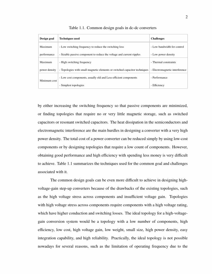
Table 1.1. Common design goals in dc-dc converters
Design goal Techniques used Challenges
Maximum
performance
- Low switching frequency to reduce the switching loss
- Sizable passive component to reduce the voltage and current ripples
- Low bandwidth for control
- Low power density
Maximum
power density
- High switching frequency
- Topologies with small magnetic elements or switched capacitor techniques
- Thermal constraints
- Electromagnetic interference
Minimum cost- Low cost components, usually old and Less-efficient components
- Simplest topologies
- Performance
- Efficiency
by either increasing the switching frequency so that passive components are minimized,
or finding topologies that require no or very little magnetic storage, such as switched
capacitors or resonant switched capacitors. The heat dissipation in the semiconductors and
electromagnetic interference are the main hurdles in designing a converter with a very high
power density. The total cost of a power converter can be reduced simply by using low-cost
components or by designing topologies that require a low count of components. However,
obtaining good performance and high efficiency with spending less money is very difficult
to achieve. Table 1.1 summarizes the techniques used for the common goal and challenges
associated with it.
The common design goals can be even more difficult to achieve in designing high-
voltage-gain step-up converters because of the drawbacks of the existing topologies, such
as the high voltage stress across components and insufficient voltage gain. Topologies
with high voltage stress across components require components with a high voltage rating,
which have higher conduction and switching losses. The ideal topology for a high-voltage-
gain conversion system would be a topology with a low number of components, high
efficiency, low cost, high voltage gain, low weight, small size, high power density, easy
integration capability, and high reliability. Practically, the ideal topology is not possible
nowadays for several reasons, such as the limitation of operating frequency due to the

3
losses incurred in the magnetic cores [3, 4] and the high cost of the efficient components
and new technologies [5, 6]. In renewable energy applications, the dc-dc topologies need
to have specific features, such as drawing continuous and smooth input current and the
ability to integrate several different types of power sources. Interleaved high-voltage-gain
converters can be fed by several independent voltage sources and have high ac components
due to interleaving on the input current, which makes them filtered out easily, and obtain an
accurate measurement of the input current to perform maximum power point tracking.
1.2. LITERATURE REVIEW
1.2.1. Conventional Boost Converter. The conventional boost converter is the
simplest step-up dc-dc topology. It has only four power-stage elements: an inductor, a
low-side MOSFET, a diode, and an output capacitor, as shown in Figure 1.1 [7–9]. The
ideal voltage gain of the converter is given by
Vo
Vin=
11 − d
(1.1)
where d is the duty cycle, which is the percent of ON time to the switching time period.
The conventional boost converter, in theory, can provide a high voltage gain at an extremely
high duty cycle, but practically speaking, it cannot be used as a high-voltage-gain converter
because of several reasons. First, working with extremely high duty cycles compromises
the efficiency and increases the voltage stress across components. Figure 1.2 shows that
voltage gain and efficiency versus the duty cycles considering only the conduction loss of the
inductor, which is normalized to the output power. The high voltage gain is limited to duties
higher than 0.9 andwith low efficiency. Considering other conduction losses of the switches,
the voltage gain is significantly reduced and the efficiency is severely compromised. The
output diode has to block the output voltage, and in high power applications, it may suffer
4
QR
+
vo _
CoVin
L D
Figure 1.1. The conventional boost converter
from the reverse recovery phenomena. Another disadvantage is that the magnetic element
that ensures continuous conduction mode would be massive, which increases the weight of
the converter and decreases the power density. [7]
1.2.2. Cascaded and Stacked Boost Converters. Cascading two or more con-
ventional boost converters increases the voltage gain without operation at extremely high
duty cycle [10, 11]. Figure 1.3(a) shows a two-stage cascaded boost converter, which is a
quadratic boost converter with voltage gain given by
Gainideal =Vo
Vin=
1(1 − d)2
(1.2)
The efficiency of a converter with two cascaded boost converters is given by
ηoverall2 = η1η2 (1.3)
More conventional boost converter can be cascaded [12], as shown in Figure 1.3(b), and the
voltage gain of the cascaded converter is given by
Gainideal =Vo
Vin=
1(1 − d)m
(1.4)
5
D
D
Efficiency of the conventional boost converter
The voltage gain of the conventional boost converter
Figure 1.2. The efficiency and gain of the conventional boost converter considering theconduction loss of the inductor.
where m is the number of the cascaded converters. The overall efficiency of m stages can
be given by
ηoverallm =
m∏n=1
ηn (1.5)
The drawback of cascading two ormore boost converters is that the power is being processed
twice, which might compromise the overall efficiency. Another disadvantage is the voltage
stress across the active switch and diode of the output stage, which is still as high as the ones
in the conventional boost converter. Single-switch cascaded converter has the same gain
as the cascaded boost converter but with a reduced number of active switches, as shown in
Figure 1.4. Using single switch leads to fewer gate driver circuitry components and lower
overall cost. However, the stages cannot be independently controlled as in the cascaded
boost converter [2, 13–15].
6
+
Vo
_R
Io
D1L1
+
Vo
_R
Q1
Vin
C1
+ vL _
iL Io D2L2
Q2 C2
1st stage
Vin
iL
2nd
stage mth
stage
(a)
(b)
Figure 1.3. Cascaded conventional boost converter (a) two stage (b) m stages
D1L1
+
Vo
_R
Q1Vin
C1
+ vL _
iL Io DoL2
Co
D2
C2
L3
D1L1
+
Vo
_R
Q1
VinC1
+ vL1 _
iL Io DoL2
Co
D2
D3
(a)
(b)
+ vL2 _
Figure 1.4. Single-switch multistage boost converter (a) two stages (b) three stages

7
RL
QVin
L1
L2C2
C1
D1 D2
D3 RL
QVin
L1
L2
L3
L4C4
C3
C2
C1
D1 D2
D3 D4
D5 D6
D7
(a) (b)
output stage
Intermediate stage
+
+ +
+
+
+
Figure 1.5. Stacked boost converter a) Quadratic b) Quartic
Stacking two or more converters means that the output voltage equals the sum of
converters output. Several stacked converters are introduced in the literature to increase
the voltage gain [16–19]. Figure 1.5 shows an example of a stacked converter [20]. The
example converter has gain ofVo
Vin=
1(1 − d)n
(1.6)
where n is the number of series capacitors. The drawbacks of this type of converter is the
voltage balance across the output capacitors if they have large numbers.
1.2.3. Three-level Boost Converter. Three-level boost was first introduced to mit-
igate the voltage stress across the output diode of the conventional boost converter and
reduce the size of magnetic elements by increasing the effective frequency [21]. The three-
level boost converter consists of an inductor, two active switches, two diodes, two output
capacitors and a floating output, as shown in Figure 1.6(a). The converter has three modes
of operation as shown in Figure 1.6(b-d), and their sequence control depends on the voltage
balance between the output capacitors [22–25]. By defining the duty cycle with respect
8
D1L
+
Vo
_
R
Q1
VinQ2 C2
D2
C1
+ vL _
iL Io D1L
+
Vo
_
R
Q1
VinQ2 C2
D2
C1
+ vL _
iL Io
D1L
+
Vo
_
R
Q1
VinQ2 C2
D2
C1
+ vL _
iL Io D1L
+
Vo
_
R
Q1
VinQ2 C2
D2
C1
+ vL _
iL Io
(a) (b)
(c) (d)
+
+
+
+
+
+
+
+
Figure 1.6. Three level boost converter a) schematic b) equivalent circuit to mode 1 whereboth active switches are ON c) equivalent circuit to mode 2 d) equivalent circuit to mode 3
to the switching frequency, the voltage gain of this converter is the same as the one of the
conventional boost converter. Still this converter is impracticable to use for applications
that necessitate high-voltage-gain converters because of the insufficient voltage gain.
1.2.4. Isolated Converters. Isolated converters can be used to increase the voltage
by increasing the turns ratio of the transformer or the coupled inductor [26–28]. Isolated
converters can be categorized based on the symmetry of the magnetic cycle of isolation de-
vice in the B-H loop [28]. Converters with an asymmetrical magnetic cycle, such as flyback
and forward converters, where the magnetic operating point of the isolation device remains
in the same quadrant. Converters with symmetrical magnetic cycles include the half-bridge
converter, dual active bridge converter, full-bridge converter, and push-pull converter. Fig-
ure 1.7 shows the circuit diagram of some conventional isolated converters, which can be
found in the literature [7, 8]. Isolated converters are required in applications where safety
is crucial, such as medical devices. However, in other applications, non-isolated dc-dc
topologies are more suitable because non-isolated converters have higher power density,

9
Q2
Q1
Vin
Co
R
Lo
D1
D2
C2
C1
VinRLN1
Do
Q1
CoN2
Q2
D1
D2
VinN1
Q1
N2
Q2
D1
D2
RL
D3
CoD4
Do
Q1
Q2
Q3
Q4
Vin
Co
R
D1
D2
LsVin
Q1
Q2
Q3
Q4
Q5
Q6
Q7
Q8
+ Co RN1 N2
(a) (b) (c)
(d) (e)
Figure 1.7. Examples of isolatedDc-dc topologies converter a) two-switch flyback converterb) two-switch forward converter c) Voltage-fed half-bridge converter d) dual active bridgeconverter e) Full-bridge converter
smaller size, and lower weight than the isolated ones. The voltage stress across switches in
the isolated converters due to the spikes instigated by the leakage inductance. Therefore,
energy circulation circuits are necessary.
1.2.5. Switched Capacitors and Hybrid Boost Converters. Switched capacitors
(SCs) mainly consist of active switches and capacitors, and they can boost the voltage by
charging and discharging capacitors. SC circuits do not use magnetic storage elements
to transfer energy and therefore would significantly increase the power density and reduce
the size and weight of the converter. Moreover, the SC circuit can be fabricated into an
integrated chip (IC) and used in portable low-power electronics. Figure 1.8 shows examples
of the most common SC circuits [29–32]. The disadvantage of using SC circuits is the
regulation and the inherent losses. This type of circuit suffers from the discontinuity of
the input currents and usually has a fixed output without the ability to increase the voltage
using the pulse width modulation signal. Although several papers presented SC converters
to have a variable output voltage, such as in [33, 34], the resolution of the conversion ratio
is still limited.
10
Vin
Q1
Q2
C2
Q1
Q2 C1
CoR
Q1
Q2
Q1
Q2 C3
Vin
Q1
Q2
Q1
Q2 C2
CoR
Q1 Q2
Q1
C2
Vin
Q2
Q1
Q2 C1
C2
+
v _
C2R
+
vo _
Q2
C1
+
v _
Q1
C1
Q1 Q1
Co
+
v _
Co R
Q1
Q3Q4
Q2
Q5 Q9Q8Q7Q6
C1
C3
C2
C4
Vin
+
+
+
+
(a) (b)
(c) (d)
+ +
+
+
Figure 1.8. Example of common switched capacitor circuits a) Cascaded voltage doublerb) Fibonacci SC c) Dickson SC d) Series parallel SC
(a)
Q1
L1
Vin
+ v _iL
L1
RC1
C2
C3
C4
C5
+ + +
+ +
D1 D2 D3 D4 D5
Cockcroft-Walton voltage multiplier Boost converter
(b)
Q1
L1
Vin
+ v _iL
L1
RC1
C2
C3
C4
C5
+
+ +
D1 D2 D3 D4 D5
Dickson voltage multiplier Boost converter
+
+
Figure 1.9. Hybrid boost converter with a) Cockcroft-walton VMC b) Dickson VMC
Hybrid boost converters combine the switched capacitor or voltage multiplier cell
with the CBC to increase the overall voltage gain, reduce the voltage stress across the
switches, and reduce the critical inductance. A typical configuration of hybrid boost
converters is shown in Figure 1.9, where the CBC is attached to Cockcroft-Walton or
Dickson VMC. Although the voltage gain of the converter is high, the efficiency of such
converter is compromised by the conduction losses in the high-current loop, which is the
loop that contains the inductor and the active switch.
1.2.6. Interleaved Boost Converters. The interleaving technique connects two or
more conventional boost converters on parallel, and switches themwith a phase shift between
phases [35, 35–37]. The current will be shared among phases, and therefore the current
11
N11Q1
Q2
*
*
*
VinR
N21
Vo+
N12 N23
N22 N13
D1 D2Do
C1 Co
C2
++
Figure 1.10. Interleaved boost converter with coupled inductors and voltage multipliers
stress is reduced as well as the conduction losses in the active switches and the magnetic
elements. Interleaving two conventional boost converters increases the frequency of the
input current and makes it easier to be filtered [38]. The voltage stress across the output
diode, however, is still the same as in the conventional boost converter [39]. The voltage
gain of the interleaved boost converter can be increased using VMC, coupled inductors, or
both, such as in [40–42]. Figure 1.10 shows a two-phase interleaved boost converter with
coupled inductors and VMCs. Using both VMC and coupled inductors, the voltage gain
becomes a function of the turns ratio, VMC stages, and the duty cycles, which makes the
converter scalable and has a wide range of output voltage. However, using coupled inductors
might require energy circulation circuits and snubbers to reduce the voltage spikes across
the switches.
The research in this dissertation ismotivated by the drawbacks of the aforementioned
topologies. Therefore, several topologies are presented to improve the existing topologies
and attain desirable features, such as low voltage stresses and low voltage and current
ripples.

12
1.3. RESEARCH CONTRIBUTION
This dissertation presents several novel DC-DC converter topologies suitable for
renewable energy applications.
Paper I introduces a family of an interleaved high-voltage-gain boost converters with
extended voltage multiplier cells. This group of converters has the capability of converting
low input voltages (12 − 48 V) to high output voltages, such as 380/400 V DC bus. The
general structure of the family consists of two stages: an interleaved boost stage and voltage
multiplier cells. Either a single or multiple independent voltage sources can feed the
interleaved boost stage, and each source can be controlled independently. The presented
converters are compared, and the way of extending the voltage multiplier cells is illustrated.
An example converter is provided, and its theory of operation and steady-state analysis is
included. Then, the analysis results are verified by simulation and experimental results.
Paper II introduces an interleaved voltage multiplier with bi-fold Dickson voltage
multiplier cells. The proposed converter in this paper also consists of two stages. However,
the proposed topology has an enhanced VMC, which has two diodes and two capacitors per
stage. The implementation bi-fold Dickson VMC and its derivation from original Dickson
VMCs are illustrated, and their applicable use in various topologies are explained. The
main advantage of the converter is the low voltage stress on all components; even the output
capacitors share the output voltage equally. Another advantage is that the input current is
shared between inductors equally regardless of the number of stages. Modes of operation
and steady-state analysis are illustrated. The converter analysis is verified by simulation
and A 200 −W hardware prototype.
Paper III Introduces a hybrid flyback and multilevel boost converters to be used as
a high voltage gain DC-DC converter. The proposed converter has advantages of vertical
interleaving, which can multiply the effective frequency seen by the magnetic element and
therefore reduce the size and magnetic storage requirement. The converter uses a flyback
transformer to increase the voltage gain by increasing the transformer turns ratio. The
13
converter has improvements over the conventional boost converter regarding the voltage
stress across active switches and the effective frequency across the magnetic element. The
proposed converter is an enhancement over the three-level boost converter for the voltage
gain and over the fly-boost converter in terms of the required magnetic storage to operate in
the continuous conduction mode.
Paper IV presents an interleaved switched-inductor boost converter with VMC. The
proposed converter utilizes the self-lift cells to increase the voltage gain and reduce the
inductors’ currents so that the size of the inductors are reduced and the conduction power
loss is also reduced. Few self-lift cells, both extended and basic, and some VMC can
be used with the proposed converter. An example converter is illustrated with two basic
self-lift cells with Cockcroft-Walton VMC cells.

14
PAPER
I. A FAMILY OF NON-ISOLATED INTERLEAVED BOOST CONVERTERSWITH VOLTAGE MULTIPLIER CELLS
Ahmad Alzahrani, Pourya Shamsi, and Mehdi Ferdowsi
Departement of Electrical and Computer Engineering
Missouri University of Science and Technology
asakw9, shamsip, [email protected]
ABSTRACT
In this paper, a family of non-isolated interleaved high-voltage-gain DC-DC con-
verters is presented. This family can be used in a wide variety of applications, such as in a
photovoltaic systems interface to a high voltage DC distribution bus in a microgrid and an
X-ray system power supply. The general structure of this family is illustrated and consists of
two stages: an interleaved boost stage and a voltage multiplier stage. The interleaved boost
stage is a two-phase boost converter, and it converts the input DC voltage to an AC square
waveform. Moreover, using the interleaved boost stage increases the frequency of the AC
components so that it can be easily filtered with smaller capacitors and, therefore, makes
the input current smoother than the one from the conventional boost converter. The voltage
multiplier cell (VMC) can be a Dickson cell, Cockcroft-Walton (CW), or a combination
of the two. The VMC stage rectifies the square-shaped voltage waveform coming from
the interleaved boost stage and converts it to a high DC voltage. Several combinations of
VMCs and how they can be extended are illustrated, and the difference between them is

15
summarized so that designers can be able to select the appropriate topology for their appli-
cations. An example of this converter family is illustrated with detailed modes of operation,
a steady-state analysis, and an efficiency analysis. The example converter was simulated to
convert 20 VDC to 400 VDC , and a 200 W hardware prototype was implemented to verify the
analysis and simulation. The results show that the example has a peak efficiency of 97% of
this family of converters and can be very suitable for interfacing renewable energy sources
to a 400 VDC DC distribution system.
Keywords: Interleaved, boost, Step-up, High-gain, DC-DC, Renewable, Microgrid, PV,
DC distribution, VMC, Modular
1. INTRODUCTION
The total power generation from renewable energy sources has been increasing
rapidly and is predicted to increase threefold in the near future [1, 2]. The transition from
using conventional and depletable energy sources in electricity generation to renewable
and sustainable sources requires adaptable power infrastructure and high-efficiency power
electronic converters. The power electronics play an indispensable role in renewable energy
sources’ integration to the main electric grid. Using highly efficient power converters
could help customers save energy and therefore increase the economic benefits [3, 4]. The
renewable energy market necessitates not only efficient, but also versatile and multipurpose,
converters. Recently, the idea of integrating a low voltage PV panel to a 400 V DC
distribution bus became a research interest due to the advantage of the DC distribution bus
over AC. The DC distribution system has less conversion units and better efficiency, power
quality, and performance than the AC distribution systems [5–9]. Integration of a single PV
panel to a 400 V DC distribution system requires a high-gain DC-DC converter [10].
Several topologies found in the literature can be used as high-gain DC-DC convert-
ers [11–22]. However, there is no superior solution for all applications. The most common
topology used to step up the input voltage is the conventional boost converter, which is the

16
most straightforward step-up converter [23]. However, the conventional boost converter
would not have enough voltage gain for integrating renewable energy sources to a 400 V ,
but if it were to have enough voltage gain, it would be only when operating at a higher
duty cycle, which might lead to the appearance of reverse recovery phenomena and low
overall efficiency, especially if the inductor DC equivalent resistance is high. Moreover, the
required inductance to stay in the continuous conduction mode is very large, and therefore,
the converter requires large and bulky magnetics [24, 25].
Cascaded boost converters were introduced to replace the conventional boost con-
verter. Such solutions increase the overall voltage gain and allow each converter to operate
at a lower duty cycle [26]. However, cascading two or more converters at least doubles
the power being processed, and that might compromise the efficiency as well. Moreover,
controlling cascaded converters requires that the output impedance of a converter be lower
than the input impedance of the following converter to ensure stability [27]. That might
lead to complications in the design and control. Stacking two or more converters helps by
sharing the power among different converters and allows the use of lower current rating
devices [28]. However, the overall voltage gain is still the same as the voltage gain of the
conventional boost converter.
Several converters can achieve higher voltage by incorporating either coupled in-
ductors or transformers [29, 30]. Such topologies increase the voltage gain by increasing
the turn ratio. However, several issues can arise. First, the leakage inductance can cause
some voltage spikes across switching devices, and that might require some voltage clamp
circuits. Second, incorporating such devices reduces the power density of the converter
and increases the weight. Furthermore, the semiconductor materials will improve rapidly,
while magnetic materials will not. Therefore, with the increase of switching frequency,
the magnetic-based components might become the most significant culprits for power loss
inside the converter. Thus, this paper introduces a family of converters that can have a
high-voltage-gain ratio, continuous current, low stress across both active and passive de-

17
vices, and high power density. The proposed family consists of two stages: an interleaved
boost stage and voltage multiplier cells. The interleaved boost stage reduces the variation of
the input current so that it is easy to obtain more accurate measurements of the PV current
to track the maximum power. The voltage multiplier cells increase the voltage gain and
reduce the voltage stresses across switching devices. Moreover, the converter can achieve a
high-voltage-gain ratio while operating at a lower duty cycle. The proposed family requires
the lower value of critical inductance to keep the converter operating in the continuous
conduction mode (CCM). The rest of the paper is structured as follows: Section 2 provides
the theory of operation and the general structure of the proposed family. Section 3 presents
different variations of the converter belonging to the proposed family. In Section 4, an
example of the proposed converter is given and analyzed. In Section 5 and 6, the simula-
tion and experimental results of the example converter are provided, respectively. Finally,
conclusions and future work are described in Section 7.
2. THEORY OF OPERATION AND GENERAL STRUCTURE OF THEPROPOSED FAMILY
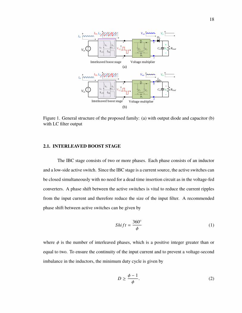
The general structure of the proposed family is shown in Figure 1, which consists of
an interleaved boost stage followed by a voltage multiplier cell, and then it is either filtered
using an output diode and capacitor capacitor as in Figure 1(a) or using an LC filter as
shown in Figure 1(b). By using an output diode and a capacitor filter, the output of VMC
is further increased by 11−d but the output current is discontinuous. On the contrary, when
using an LC filter, the output voltage of the VMC is not increased, but the output current
is continuous if the inductor is large enough to operate in the CCM mode. Several papers
present members belonging to the proposed family [31–37]. However, no information about
extending the VMC cells or the interleaved boost phases has been reported. The following
sections present details about each stage of the proposed family.
18
+_
IL1, IL2
Iin
Vxy
Vo
x
y
RloadVin
D1
C1 C2
D2
L1 L2
S1 S2
iL1iL2
Interleaved boost stage Voltage multiplier
Do
Co
w
z
Vwz
+_
IL1, IL2
Iin
Vxy
Vo
x
y
RloadVin
D1
C1 C2
D2
L1 L2
S1 S2
iL1iL2
Interleaved boost stage Voltage multiplier
Lo
Co
w
z
Vwz
(a)
(b)
+
Vo
_
+
Vo
_
Figure 1. General structure of the proposed family: (a) with output diode and capacitor (b)with LC filter output
2.1. INTERLEAVED BOOST STAGE
The IBC stage consists of two or more phases. Each phase consists of an inductor
and a low-side active switch. Since the IBC stage is a current source, the active switches can
be closed simultaneously with no need for a dead time insertion circuit as in the voltage-fed
converters. A phase shift between the active switches is vital to reduce the current ripples
from the input current and therefore reduce the size of the input filter. A recommended
phase shift between active switches can be given by
Shi f t =360
φ(1)
where φ is the number of interleaved phases, which is a positive integer greater than or
equal to two. To ensure the continuity of the input current and to prevent a voltage-second
imbalance in the inductors, the minimum duty cycle is given by
D ≥φ − 1φ
. (2)
19
Number of phases
En
erg
y s
tora
ge
red
uct
ion
(%
)
1 2 3 4 5 6 70
10
20
30
40
50
60
70
80
90
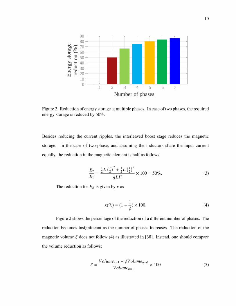
Figure 2. Reduction of energy storage at multiple phases. In case of two phases, the requiredenergy storage is reduced by 50%.
Besides reducing the current ripples, the interleaved boost stage reduces the magnetic
storage. In the case of two-phase, and assuming the inductors share the input current
equally, the reduction in the magnetic element is half as follows:
E2E1=
12 L
( I2)2+ 1
2 L( I
2)2
12 LI2
× 100 = 50%. (3)
The reduction for Eφ is given by κ as
κ(%) = (1 −1φ) × 100. (4)
Figure 2 shows the percentage of the reduction of a different number of phases. The
reduction becomes insignificant as the number of phases increases. The reduction of the
magnetic volume ζ does not follow (4) as illustrated in [38]. Instead, one should compare
the volume reduction as follows:
ζ =Volumen=1 − φVolumen=φ
Volumen=1× 100 (5)

20
where Volumen=1 is the volume of the magnetic element in a single phase converter and
Volumen=φ is the volume of the magnetic element of a multiphase converter with φ phases.
Another advantage of interleaving is that the total conduction loss in the inductors and the
active switching devices is reduced if the current is shared equally between the phases as
follows:
PLtotal=
I2L × RDC
φ, (6)
PS,condtotal =I2S,rms × RON
φ. (7)
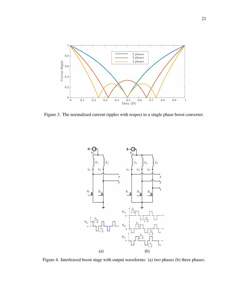
The input current ripples depend on the number of interleaved phases and the duty cycle.
Figure 3 shows the relationship between the number of stages and the normalized input
ripples. Increasing the number of phases reduces the ripples and allows ripple cancellation
to occur at multiple duty cycle values. Two phases can have one point of ripple cancellation
at the 0.5 duty cycle; while in three phases the ripple cancellation occurs at two points: the
0.25 and 0.75 duty cycles. For more phases, the duty cycle values where ripple cancellation
can occur are given by
d∆v=0 = [
1φ,2φ, ...,
φ − 1φ] (8)
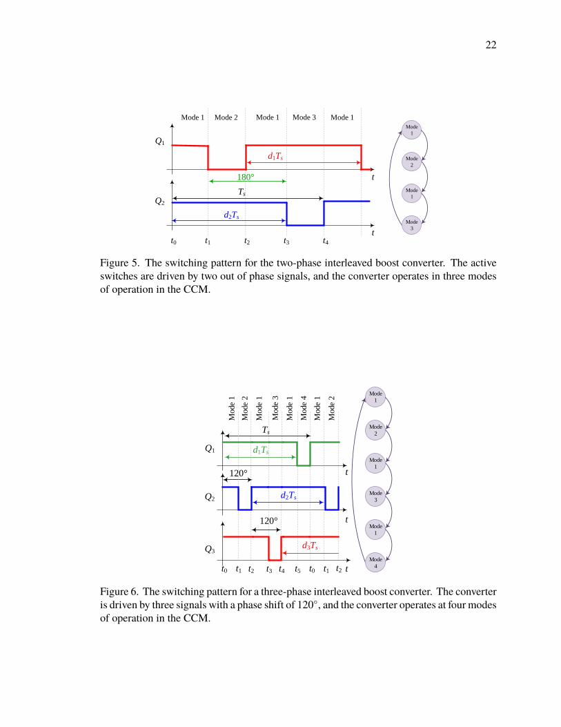
Figures 4(a) and (b) show the schematic and output waveforms of the interleaved
boost stage for two and three phases, respectively. The switching waveforms and modes
of operations are shown in Figure 5 for two phases and Figure 6 for three phases. More
phases can be used, such as in [39], but three or more phases will not have a uniform pattern
of connections to the VMC, and the permutation of variation of the topologies is large.
Therefore, the number of phases is limited to two in this paper.
21
Duty (D)0 0.1 0.2 0.3 0.4 0.5 0.6 0.7 0.8 0.9 1
Curr
ent R
ipple
0
0.2
0.4
0.6
0.8
1
2 phases3 phases
4 phases
Figure 3. The normalized current ripples with respect to a single phase boost converter.
L1 L2
S1 S2
iL1 iL2
Vin
+-
L3
iL3
x
S3
y
z
L1 L2
S1 S2
iL1 iL2
Vin
+-
x
y
Vxy
Vyz
Vxz
Vxy
0
0
0
0
1
inV
d
1
inV
d
1
inV
d
1
inV
d
1
inV
d
1
inV
d
1
inV
d
1
inV
d
(a) (b)
Figure 4. Interleaved boost stage with output waveforms: (a) two phases (b) three phases.
22
Mode 1
Q1
Q2
Mode 1 Mode 2 Mode 3
t
t
Ts
d2Ts
Mode 1
t0 t1 t2 t3 t4
180°
d1Ts
Mode
1
Mode
2
Mode
1
Mode
3
Figure 5. The switching pattern for the two-phase interleaved boost converter. The activeswitches are driven by two out of phase signals, and the converter operates in three modesof operation in the CCM.
Mode 1
Q1
Q2
Mode 1
Mode 2
Mode
4
t
t
Ts
d2Ts
Mode 1
21 0°
Mode
1
Mode
2
Mode
1
Mode
3
Mode
1
Mode
4
Q3
t0 t1 t2 t3 t4
Mode 1
Mode
3
tt5
d1Ts
21 0°
d3Ts
Mode 2
t0 t1 t2
Figure 6. The switching pattern for a three-phase interleaved boost converter. The converteris driven by three signals with a phase shift of 120, and the converter operates at four modesof operation in the CCM.
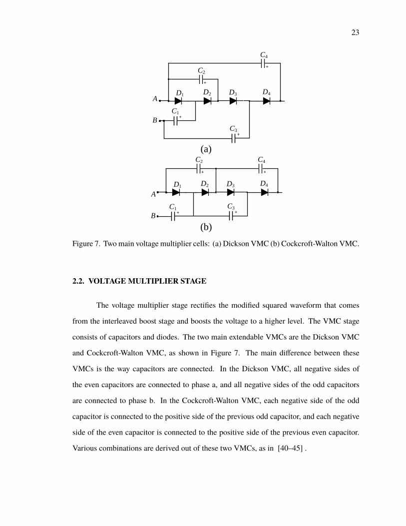
23
C2
D2D1
C1+
+
C3+
D3 D4
C4
+
C2
D2D1
C1+
+
C3+
D3 D4
C4
+
A
B
A
B
(a)
(b)
Figure 7. Twomain voltage multiplier cells: (a) Dickson VMC (b) Cockcroft-Walton VMC.
2.2. VOLTAGE MULTIPLIER STAGE
The voltage multiplier stage rectifies the modified squared waveform that comes
from the interleaved boost stage and boosts the voltage to a higher level. The VMC stage
consists of capacitors and diodes. The two main extendable VMCs are the Dickson VMC
and Cockcroft-Walton VMC, as shown in Figure 7. The main difference between these
VMCs is the way capacitors are connected. In the Dickson VMC, all negative sides of
the even capacitors are connected to phase a, and all negative sides of the odd capacitors
are connected to phase b. In the Cockcroft-Walton VMC, each negative side of the odd
capacitor is connected to the positive side of the previous odd capacitor, and each negative
side of the even capacitor is connected to the positive side of the previous even capacitor.
Various combinations are derived out of these two VMCs, as in [40–45] .
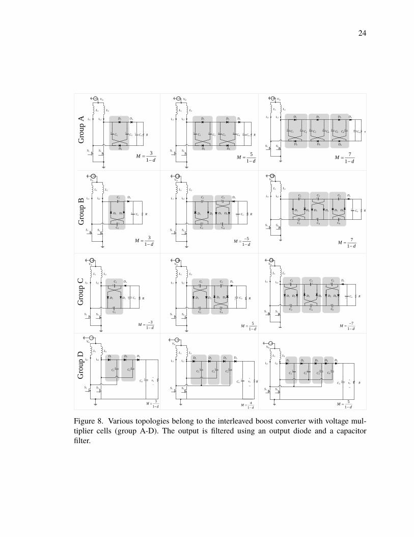
24
L1 L2
S1 S2
iL1 iL2 D1
C1
Vin
+-
C2
D2
RCo
Do
L1 L2
S1 S2
iL1 iL2 D1
C1
D3
C4
Vin
+-
C2
D2 D4
C3 RCo
Do
L1 L2
S1 S2
iL1 iL2 D1
C1
D3
C4
Vin
+-
D5
C2
D2
C5
D4
C3
D6
C6 RCo
Do
L1 L2
S1 S2
iL1 iL2
D1
C1
D2
C4
Vin
+-
D3
C2
D4
C3
RCo
Do
L1 L2
S1 S2
iL1 iL2
D1
C1
D2
C4
Vin
+-
D3
C2
D4
C3
RCo
Do
L1 L2
S1 S2
iL1 iL2
D1
C1
D2
C4
Vin
+-
D3
C2
D4
C5
D5
C3
D6
C6
RCo
Do
L1 L2
S1 S2
iL1
D1
C1
D2
C4
Vin
+-
D3
C2
D4
C5
D5
C3
D6
C6
RCo
DoiL2
R
L1 L2
S1 S2
+
vo
_
iL1 iL2
D1
C1
D2
C2
D3
Vin
+-
Co
Do
C3
R
L1 L2
S1 S2
+
vo
_
iL1 iL2
D1
C1
D2
C2
D3
Vin
+-
Co
DoD4
C3 C4
3
1M
d
5
1M
d
7
1M
d
3
1M
d
5
1M
d
7
1M
d
3
1M
d
5
1M
d
7
1M
d
4
1M
d
5
1M
d
+++ + + + + +
+ + + + + + +
+
+
+
++
+
+
+
+
+
+
+
+
++
+
+
+
+
+
+
+
++
+ + +
+
+ + + +
+
+
L1 L2
S1 S2
iL1 iL2
D1
C1
D2
Vin
+-
C2
RCo
Do
+
+
L1 L2
S1 S2
+
vo
_
iL1 iL2
D1
C1
D2
C2
Vin
+-
Co
Do
3
1M
d
+ +
+
L1 L2
S1 S2
iL1 iL2
D1
C1
D2
Vin
+-
C2
RCo
Do
+
+
+
Gro
up
AG
rou
p B
Gro
up
CG
rou
p D
Figure 8. Various topologies belong to the interleaved boost converter with voltage mul-tiplier cells (group A-D). The output is filtered using an output diode and a capacitorfilter.

25
C2b
D1b D2b
+
C1b
C2a
D2aD1a
+
C2
D2D1
C1
+
+
C3
+
D3
R
L1 L2
S1 S2
+
vo
_
iL1
C2
Vin
+-
Co
DoD2D1
C1
iL2
R
L1 L2
S1 S2
+
vo
_
iL1
Vin
+-
Co
DoiL2
R
L1 L2
S1 S2
+
vo
_
iL1
Vin
+-
Co
DoiL2
R
L1 L2
S1 S2
+
vo
_
iL1 iL2D1a D2a
Vin
+-
Co
Do
C1a
C3a
C3b
C1b
D1b D2b
R
L1 L2
S1 S2
+
vo
_
iL1 iL2D1a D2a
Vin
+-
Co
D3a Do
C1a C2a C3a
C3bC1b C2b
D1b D2b D3b
R
L1 L2
S1 S2
+
vo
_
iL1 iL2D1a
Vin
+-
Cout
Do
C1a
C1b
D1b
R
L1 L2
S1 S2
+
vo
_
iL1
Vin
+-
Co
DoiL2
R
L1 L2
S1 S2
+
vo
_
iL1
Vin
+-
Co
DoiL2
R
L1 L2
S1 S2
+
vo
_
iL1
Vin
+-
Co
Do
iL2
R
L1 L2
S1 S2
+
vo
_
iL1
Vin
+-
Co
Do
iL2
R
L1 L2
S1 S2
+
vo
_
iL1
Vin
+-
Co
Do
iL2
D1a
C1a
D1a D2a
C2a
D1a D2a
C2a
C3a
D3a
3
1M
d
4
1M
d
5
1M
d
3
1M
d
5
1M
d
7
1M
d
3
1M
d
5
1M
d
7
1M
d
4
1M
d
6
1M
d
5
1M
d
++++
+
+
+ +
++
+
+ + +
+++
+
+
+
+
+
+
+
+ +
+
+ + +
+
C2
D2D1
C1
+
+
C3
+
D3D4
C4
+
+
C1a
+
C2a
D2aD1a
+
+
R
L1 L2
S1 S2
+
vo
_
iL1
Vin
+-
Co
DoiL2
+
C2a
D2aD1a
+
+
C2b
D1b D2b
+
C1b
+
C1b
C1a
D3a
C3a
C2b
C3b
C1b
C1a
C1b
C1a
C1b
C1a
D1b D2b D3b
C3b
+
+
+C3b
C2bC4bC2b
D1b D2b D3b D4b
D1b D2b D3bD1b D2b D3b D4b
C3b
C2b C4b
+ +
+
+
C3a
C4a
D3a D4a
Gro
up E
Gro
up F
Gro
up G
Gro
up H
Figure 9. Various topologies belong to the interleaved boost converter with voltage multi-plier cells (group E-H): with an output diode and a capacitor filter.
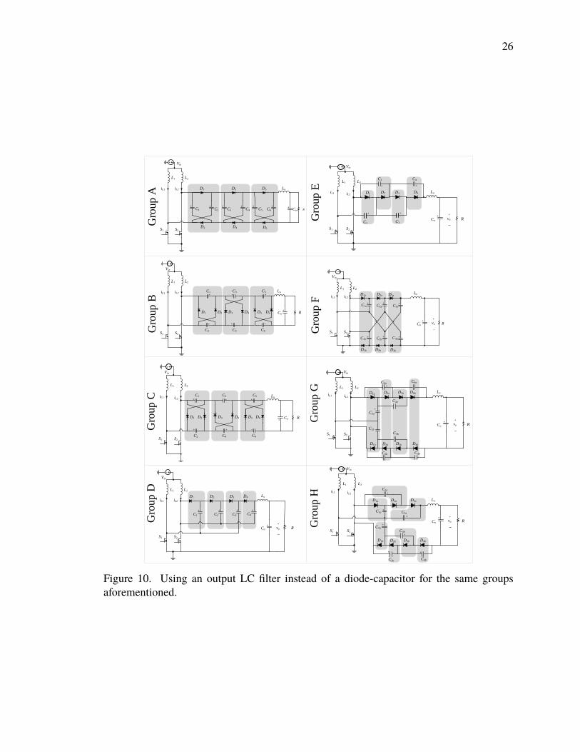
26
L1 L2
S1 S2
iL1 iL2 D1
C1
D3
C4
Vin
+-
D5
C2
D2
C5
D4
C3
D6
C6 RCo
Lo
L1 L2
S1 S2
iL1 iL2
D1
C1
D2
C4
Vin
+-
D3
C2
D4
C5
D5
C3
D6
C6
RCo
Lo
L1 L2
S1 S2
iL1
D1
C1
D2
C4
Vin
+-D3
C2
D4
C5
D5
C3
D6
C6
RCo
LoiL2
R
L1 L2
S1 S2
+
vo
_
iL1 iL2
D1
C1
D2
C2
D3
Vin
+-
Co
LoD4
C3 C4
+ + + + + + +
+
+
+
+
+
+
+
+
+
+
+
+
+
+
+ + + +
+
Gro
up A
Gro
up B
Gro
up C
Gro
up D
Gro
up E
Gro
up F
Gro
up G
Gro
up H
C2
D2D1
C1
+
+
C3
+
D3
R
L1 L2
S1 S2
+
vo
_
iL1
Vin
+-
Co
LoiL2
R
L1 L2
S1 S2
+
vo
_
iL1 iL2D1a D2a
Vin
+-
Co
D3aLo
C1a C2a C3a
C3bC1b C2b
D1b D2b D3b
R
L1 L2
S1 S2
+
vo
_
iL1
Vin
+-
Co
Lo
iL2
D1a D2a
C2a
C3a
D3a
+
+ + +
+++
+
+
+
+
+
D4
C4
+
R
L1 L2
S1 S2
+
vo
_
iL1
Vin
+-
Co
Lo
iL2
+
C2a
D2aD1a
+
+
C1b
C1a
C1b
C1a
C3b
C2bC4b
D1b D2b D3b D4b
D1b D2b D3b D4b
C3b
C2b C4b
+ +
+
+
C3a
C4a
D3a D4a
Figure 10. Using an output LC filter instead of a diode-capacitor for the same groupsaforementioned.
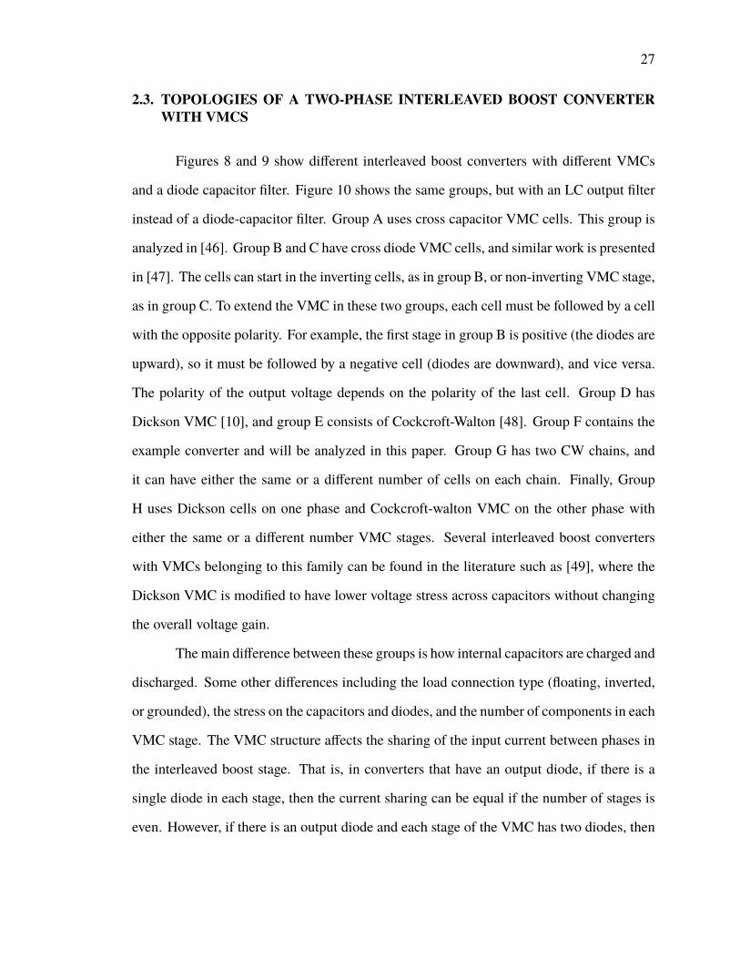
27
2.3. TOPOLOGIES OF A TWO-PHASE INTERLEAVED BOOST CONVERTERWITH VMCS
Figures 8 and 9 show different interleaved boost converters with different VMCs
and a diode capacitor filter. Figure 10 shows the same groups, but with an LC output filter
instead of a diode-capacitor filter. Group A uses cross capacitor VMC cells. This group is
analyzed in [46]. Group B and C have cross diode VMC cells, and similar work is presented
in [47]. The cells can start in the inverting cells, as in group B, or non-inverting VMC stage,
as in group C. To extend the VMC in these two groups, each cell must be followed by a cell
with the opposite polarity. For example, the first stage in group B is positive (the diodes are
upward), so it must be followed by a negative cell (diodes are downward), and vice versa.
The polarity of the output voltage depends on the polarity of the last cell. Group D has
Dickson VMC [10], and group E consists of Cockcroft-Walton [48]. Group F contains the
example converter and will be analyzed in this paper. Group G has two CW chains, and
it can have either the same or a different number of cells on each chain. Finally, Group
H uses Dickson cells on one phase and Cockcroft-walton VMC on the other phase with
either the same or a different number VMC stages. Several interleaved boost converters
with VMCs belonging to this family can be found in the literature such as [49], where the
Dickson VMC is modified to have lower voltage stress across capacitors without changing
the overall voltage gain.
Themain difference between these groups is how internal capacitors are charged and
discharged. Some other differences including the load connection type (floating, inverted,
or grounded), the stress on the capacitors and diodes, and the number of components in each
VMC stage. The VMC structure affects the sharing of the input current between phases in
the interleaved boost stage. That is, in converters that have an output diode, if there is a
single diode in each stage, then the current sharing can be equal if the number of stages is
even. However, if there is an output diode and each stage of the VMC has two diodes, then
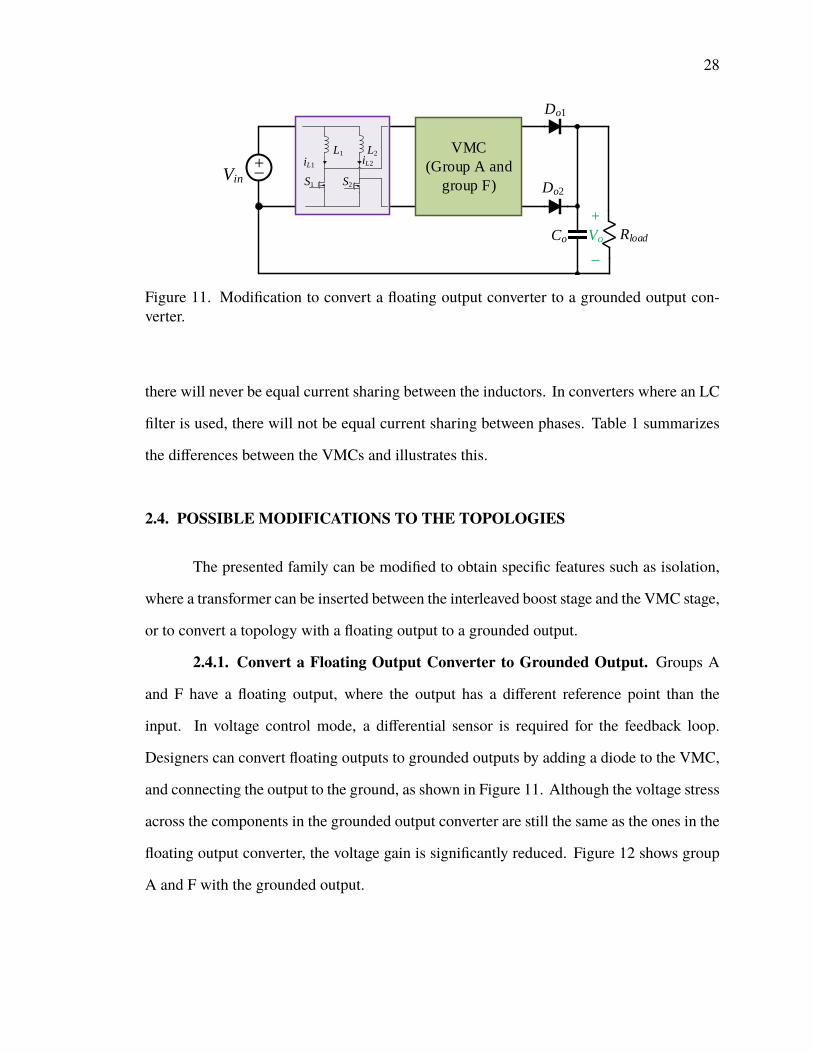
28
VMC
(Group A and
group F)
+_
Rload
Vin
L1 L2
S1 S2
iL1iL2
Do1
Co
+
Vo
_
Do2
Figure 11. Modification to convert a floating output converter to a grounded output con-verter.
there will never be equal current sharing between the inductors. In converters where an LC
filter is used, there will not be equal current sharing between phases. Table 1 summarizes
the differences between the VMCs and illustrates this.
2.4. POSSIBLE MODIFICATIONS TO THE TOPOLOGIES
The presented family can be modified to obtain specific features such as isolation,
where a transformer can be inserted between the interleaved boost stage and the VMC stage,
or to convert a topology with a floating output to a grounded output.
2.4.1. Convert a Floating Output Converter to Grounded Output. Groups A
and F have a floating output, where the output has a different reference point than the
input. In voltage control mode, a differential sensor is required for the feedback loop.
Designers can convert floating outputs to grounded outputs by adding a diode to the VMC,
and connecting the output to the ground, as shown in Figure 11. Although the voltage stress
across the components in the grounded output converter are still the same as the ones in the
floating output converter, the voltage gain is significantly reduced. Figure 12 shows group
A and F with the grounded output.

29
L1 L2
S1 S2
iL1 iL2 D1
C1
D3
C4
Vin
+-
C2
D2 D4
C3
RCo
Do1
+ + + +
+
Do2 R
L1 L2
S1 S2
+
vo
_
iL1 iL2
D1a D2a
Vin
+-
Co
Do1
C1a
C3a
C3b
C1b
D1b D2b
+ +
++
+
Do2
(a) (b)
Figure 12. Group A and F can be converted to have a grounded output. Both have an idealvoltage gain of M = N+1
1−d , which isN
1−d less than the ones with floating outputs.
+_ RloadVin
D1
C1 C2
D2
L1 L2
S1 S2
iL1iL2
Interleaved boost stage Voltage multiplier
Do
Co
+
Vo
_
Isolation
N1:N2
Figure 13. The presented family can be modified by adding an isolation device to meet theisolation requirement and improve the voltage gain.
2.4.2. Modification to Make the Converter Isolated. This family can easily be
a family of isolated converters by adding a transformer or coupled inductors between the
interleaved boost stage and the VMC stage, as shown in Figure 13. After adding the isolation
device with an N1 : N2 turns ratio, the voltage gain can be calculated as
Misolated = Mnonisolated ×N2N1
(9)

30
L1 L2
S1 S2
iL1 iL2 D1
C1
Vin
+-
C2
D2
RCo
Do
+++
D3 D4 D5
+
+
+
C4
C3 C5
Figure 14. Example of nonuniform topologies. The converter features two different typesof VMCs, a cell from group F and Cockcroft-Walton VMC.
2.4.3. ConnectingTwoDifferentVMCs toObtain theOverall NonuniformCon-
verter. Extra possible combinations of different voltagemultiplier cells can be derived, e.g.,
but will be unable to expand one or both VMCs. The analysis of nonuniform converters is
performed on a case by case basis. Figure 14 shows an example of nonuniform combina-
tions. The converter consists of one cell from group F followed by Cockcroft-Walton cells.
3. MODES OF OPERATION AND STEADY-STATE ANALYSIS OF ANEXAMPLE CONVERTER
This section presents a detailed analysis of the circuit, shown in Figure 15. The
converter is driven by two 180 out phase signals, as shown in Figure 6. The equivalent
circuit of the three modes is shown in Figure 16 (a-c). The analysis was performed with
several assumptions: 1) All components are ideal; 2) The capacitors are large enough that
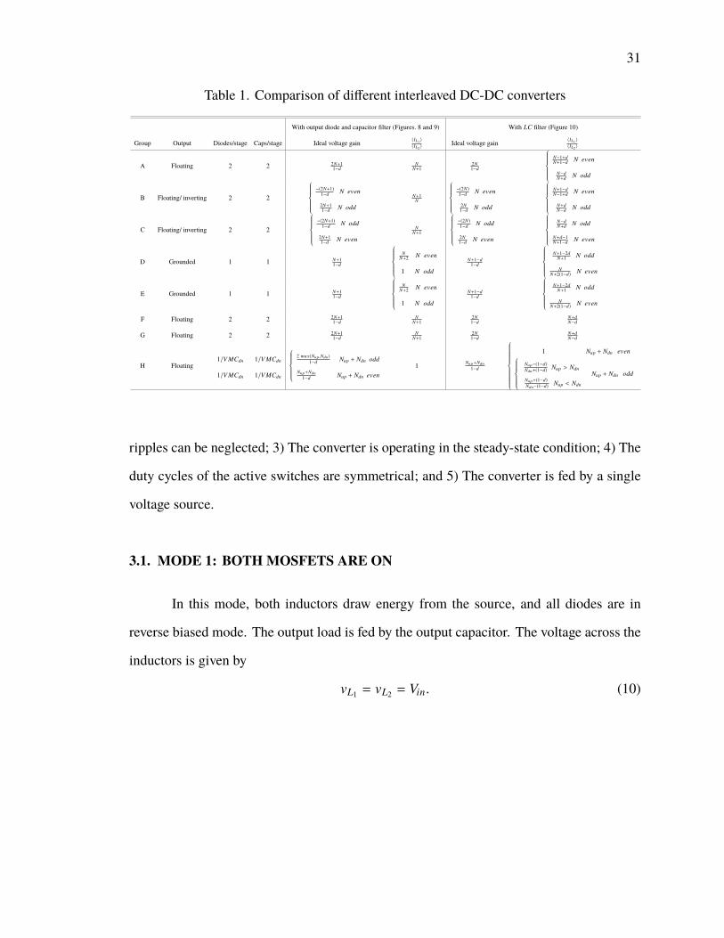
31
Table 1. Comparison of different interleaved DC-DC converters
With output diode and capacitor filter (Figures. 8 and 9) With LC filter (Figure 10)
Group Output Diodes/stage Caps/stage Ideal voltage gain 〈IL1 〉
〈IL2 〉Ideal voltage gain 〈IL1 〉
〈IL2 〉
A Floating 2 2 2N+11−d
NN+1
2N1−d
N−1+dN+1−d N even
N−dN+d N odd
B Floating/ inverting 2 2
−(2N+1)
1−d N even
2N+11−d N odd
N+1N
−(2N)1−d N even
2N1−d N odd
N+1−dN−1+d N even
N+dN−d N odd
C Floating/ inverting 2 2
−(2N+1)
1−d N odd
2N+11−d N even
NN+1
−(2N)1−d N odd
2N1−d N even
N−dN+d N odd
N+d−1N+1−d N even
D Grounded 1 1 N+11−d
N
N+2 N even
1 N odd
N+1−d1−d
N+1−2d
N+1 N odd
NN+2(1−d) N even
E Grounded 1 1 N+11−d
N
N+2 N even
1 N odd
N+1−d1−d
N+1−2d
N+1 N odd
NN+2(1−d) N even
F Floating 2 2 2N+11−d
NN+1
2N1−d
N+dN−d
G Floating 2 2 2N+11−d
NN+1
2N1−d
N+dN−d
H Floating1/V MCdn
1/V MCdn
1/V MCdn
1/V MCdn
2 max(Nup,Ndn)
1−d Nup + Ndn odd
Nup+Ndn
1−d Nup + Ndn even1 Nup+Ndn
1−d
1 Nup + Ndn evenNup−(1−d)Ndn+(1−d) Nup > Ndn
Nup+(1−d)Ndn−(1−d) Nup < Ndn
Nup + Ndn odd
ripples can be neglected; 3) The converter is operating in the steady-state condition; 4) The
duty cycles of the active switches are symmetrical; and 5) The converter is fed by a single
voltage source.
3.1. MODE 1: BOTHMOSFETS ARE ON
In this mode, both inductors draw energy from the source, and all diodes are in
reverse biased mode. The output load is fed by the output capacitor. The voltage across the
inductors is given by
vL1 = vL2 = Vin. (10)

32
R
L1 L2
S1 S2
+
vo
_
iL1 iL2D1a D2a
Vin
+-
Co
D3a Do
C1a C2a C3a
C3bC1b C2b
D1b D2b D3b
+
+
+
+
+
+
Figure 15. Example converter; an interleaved boost stage with a 3 level VMC
R
L1 L2
S1 S2
+
vo
_
iL1 iL2D1a D2a
Vin
+-
Co
D3a Do
C1a C2a C3a
C3bC1b C2b
D1b D2b D3b
+
+
+
+
+
+
R
L1 L2
S1 S2
+
vo
_
iL1 iL2D1a D2a
Vin
+-
Co
D3a Do
C1a C2a C3a
C3bC1b C2b
D1b D2b D3b
++
+
+
+ +
R
L1 L2
S1 S2
+
vo
_
iL1 iL2D1a D2a
Vin
+-
Co
D3a Do
D1b D2b D3b
C1a C2a C3a
C3bC1b C2b
+
+
+
+
+
+
(a)
(c)
(b)
Figure 16. Modes of operation of the example converter; (a) mode 1 (b) mode 2 (c) mode 3
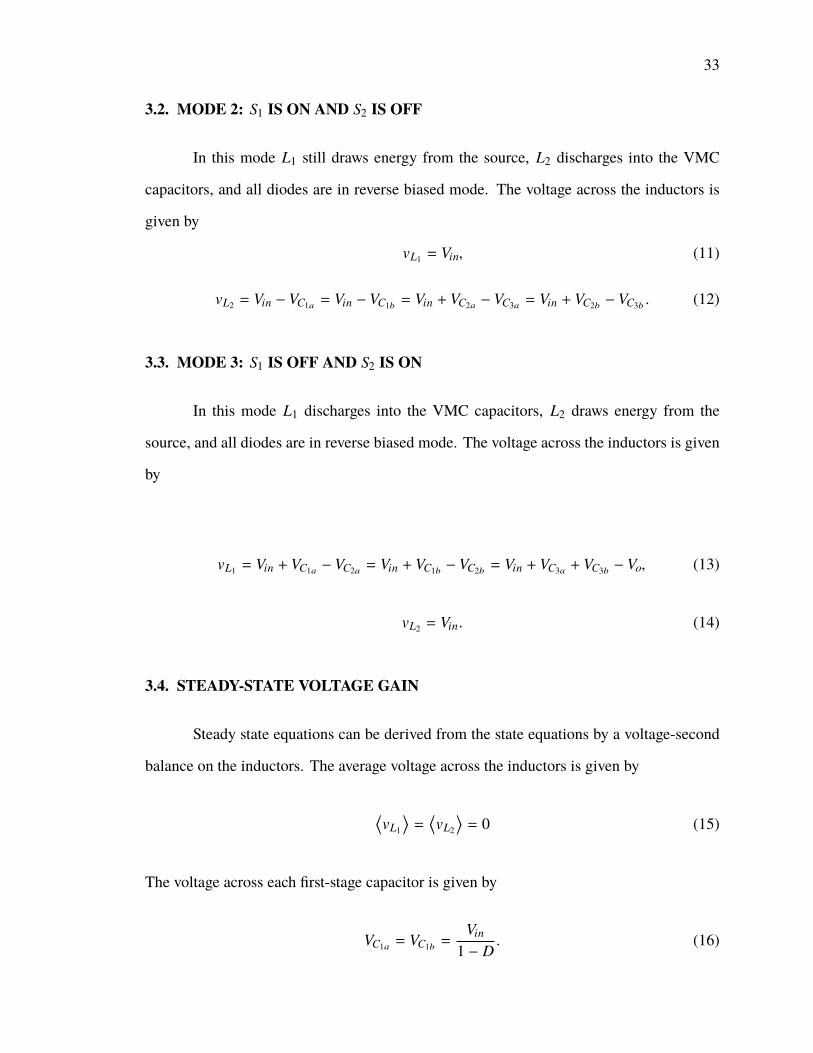
33
3.2. MODE 2: S1 IS ON AND S2 IS OFF
In this mode L1 still draws energy from the source, L2 discharges into the VMC
capacitors, and all diodes are in reverse biased mode. The voltage across the inductors is
given by
vL1 = Vin, (11)
vL2 = Vin − VC1a = Vin − VC1b = Vin + VC2a − VC3a = Vin + VC2b − VC3b . (12)
3.3. MODE 3: S1 IS OFF AND S2 IS ON
In this mode L1 discharges into the VMC capacitors, L2 draws energy from the
source, and all diodes are in reverse biased mode. The voltage across the inductors is given
by
vL1 = Vin + VC1a − VC2a = Vin + VC1b − VC2b = Vin + VC3a + VC3b − Vo, (13)
vL2 = Vin. (14)
3.4. STEADY-STATE VOLTAGE GAIN
Steady state equations can be derived from the state equations by a voltage-second
balance on the inductors. The average voltage across the inductors is given by
⟨vL1
⟩=
⟨vL2
⟩= 0 (15)
The voltage across each first-stage capacitor is given by
VC1a = VC1b =Vin
1 − D. (16)
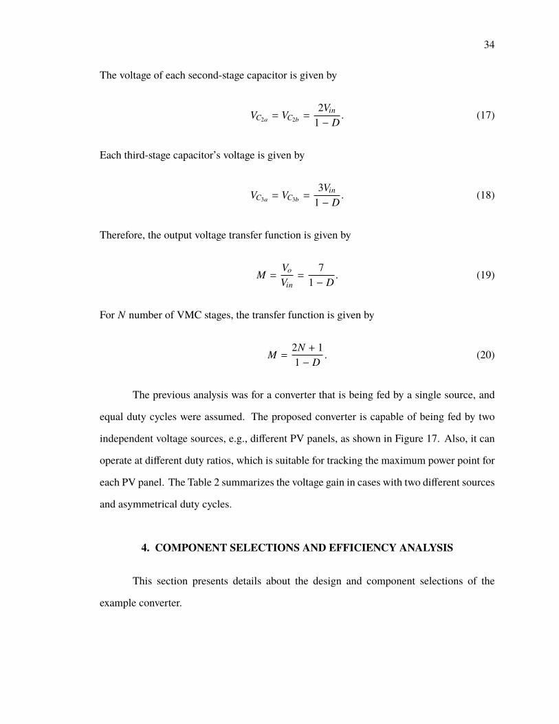
34
The voltage of each second-stage capacitor is given by
VC2a = VC2b =2Vin
1 − D. (17)
Each third-stage capacitor’s voltage is given by
VC3a = VC3b =3Vin
1 − D. (18)
Therefore, the output voltage transfer function is given by
M =Vo
Vin=
71 − D
. (19)
For N number of VMC stages, the transfer function is given by
M =2N + 11 − D
. (20)
The previous analysis was for a converter that is being fed by a single source, and
equal duty cycles were assumed. The proposed converter is capable of being fed by two
independent voltage sources, e.g., different PV panels, as shown in Figure 17. Also, it can
operate at different duty ratios, which is suitable for tracking the maximum power point for
each PV panel. The Table 2 summarizes the voltage gain in cases with two different sources
and asymmetrical duty cycles.
4. COMPONENT SELECTIONS AND EFFICIENCY ANALYSIS
This section presents details about the design and component selections of the
example converter.
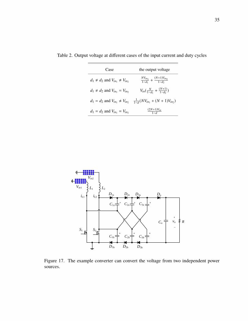
35
Table 2. Output voltage at different cases of the input current and duty cycles
Case the output voltage
d1 , d2 and Vin1 , Vin2NVin11−d1+(N+1)Vin2
1−d2
d1 , d2 and Vin1 = Vin2 Vin(N
1−d1+(N+1)1−d2)
d1 = d2 and Vin1 , Vin21
1−d (NVin1 + (N + 1)Vin2)
d1 = d2 and Vin1 = Vin2(2N+1)Vin
1−d
R
L1 L2
S1 S2
+
vo
_
iL1 iL2D1a D2a
Vin2
Co
D3a Do
C1a C2a C3a
C3bC1b C2b
D1b D2b D3b
+
+
+
+
+
+
Vin1
Figure 17. The example converter can convert the voltage from two independent powersources.

36
4.1. INDUCTOR SELECTION
The critical inductance that ensures CCM operation is given by
L1crit =Rd(1 − d)2
N(2N + 1) fs, (21)
L2crit =Rd(1 − d)2
(N + 1)(2N + 1) fs. (22)
However, to select an inductor based on the percentage of the ripple, one should follow
L1 =Vind∆iL1 fs
, (23)
L2 =Vind∆iL2 fs
. (24)
The average current passing through inductors L1 and L2 is as follows:
IL1,avg =Vo
RN
(1 − d), (25)
IL2,avg =Vo
RN + 1(1 − d)
. (26)
The peak currents can be calculated as follows:
IL1,pk =Vo
RN
(1 − d)+
dVin
L fs, (27)
IL2,pk =Vo
RN + 1(1 − d)
+dVin
L fs. (28)
The RMS currents are given by
IL1,rms =
√√√(VoN
R(1 − d)
)2+
(dVin
2√
3L fs
)2
, (29)

37
IL2,rms =
√√√(Vo(N + 1)R(1 − d)
)2+
(dVin
2√
3L fs
)2
. (30)
4.2. ACTIVE SWITCHES SELECTION
The voltage stress across MOSFETs can be calculated by
VS1 = VS2 =Vin
1 − d(31)
and the average current passing through the MOSFETs is given by
IS1,avg =Vo
R
(dN
1 − d+ N + 1
), (32)
IS2,avg =Vo
R
(d(N + 1)
1 − d+ N
). (33)
The root mean square value of the switch current is given by
IS1rms=
√(Vo
R
(dN1−d + N + 1
))2+
((2N+1)Vin(2d−1)
2L fs
)2, (34)
IS2,rms =
√(Vo
R
(d(N+1)
1−d + N))2+
((2N+1)Vin(2d−1)
2L fs
)2. (35)
4.3. DIODE SELECTION
The voltage stress across the diodes is a function of the number of stages. The
voltage stress is reduced as the number of stages increases, and that comes at the cost of
efficiency. The voltage stress is given by
VD =2Vo
(2N + 1). (36)

38
The average current passing through each diode can be calculated by
IDN ,avg = Io (37)
and the RMS value of the diodes can be calculated as
ID,rms = Io
√1
1 − d. (38)
4.4. CAPACITOR SELECTION
The capacitor is selected based on the tolerated voltage ripple, and it can be calculated
using the following equation
C =Io(1 − d)
f∆v. (39)
The RMS value of the current passing through the output capacitor is given by
ICo,rms = Io
√d
(1 − d)(40)
and the RMS current of the other capacitors can be calculated by
ICn,rms = Io(1 +
√d
(1 − d)) (41)
5. POWER LOSSES AND EFFICIENCY ANALYSIS
The power losses in the inductors are given by
PL = I2L1,rms
DCR1 + I2L2,rms
DCR2 (42)

39
where DCR1 and DCR2 are the DC resistance. The power losses in the active switches can
be divided into two parts: switching loss and conduction loss. The switching loss can be
calculated using the following equation:
PSW = 2(12× IL,avg × VS × (tOFF + tON ) fs
+12× fs × Coss × V2
S ). (43)
The conduction loss part is given by
PS,conduction = I2s1,rms
R1(on) + I2S2,rms
R2(on) (44)
where R1(on) and R2(on) are the drain-source resistance of S1 and S2. The power loss in
the diodes can be calculated by
PD =
N∑i=1
IDavg × VF +
N∑i=1
IDrms × r f (45)
where VF is the forward voltage of the diode, and r f is the bulk resisor. The power loss in
the capacitors due to the equivalent series resistance (ESR) is given by
PC,total = NI2Cn,rms
ESRn + I2Co,rms
ESRo. (46)
The total loss is given by
Ploss = PD,total + PC,total + PS,conduction + PSW + PL (47)
The overall efficiency of the converter is given by
η% =Po
Ploss + Po× 100. (48)
40
6. SIMULATION
The example converter was simulated in PLECS/MATLAB, with a maximum time
step of 10−7 s and tolerance of 10−3. The parameters used in the simulation are listed in
Table 3. The major waveforms are plotted in Figure 18. The voltage stress across the active
switches is 57 V . The average current on L1 and L2 is 4.28 A and 5.7 A, respectively.
The maximum voltage across the diodes is 114 V . The average and effective values of the
current passing through each diode are 0.5 A and 0.84 A. The voltage across the capacitors
is shown in Figure 19. The currents passing through the diodes and capacitors are shown in
Figure 20 and Figure 21, respectively. The first-stage capacitors C1Aand C1B have a voltage
of 57 V , the second-stage capacitors have a voltage of 114 V , and the third-stage capacitors
have a voltage of 171 V . The RMS current of the output capacitor is 0.68 A, while the other
capacitors have an RMS current of 1.18 A. The efficiency analysis was performed using the
loss equations of the components and the rating from the datasheets of the components used
for implementing the hardware prototype. The approximate loss breakdown and breakdown
percentage as a function of the output load is depicted in Figure 22. The total loss at 200 W
is about 4.98 W . The major source of loss is the conduction loss in the diodes, which counts
for about 68%. The conduction loss in the MOSFETs is about 13%, and the switching loss
is about 7% of the total loss. The conduction loss in the inductors counts for about 11%,
and the total loss caused by the ESR of the capacitors is less than 1%.
7. EXPERIMENTAL IMPLEMENTATION AND RESULTS
A 200 W hardware prototype was implemented and tested to further verify the
operation of the example converter. The components used to construct the hardware
prototype are listed in Table 4, and the experimental setup is shown in Figure 23. The
converter was designed for a nominal duty cycle of 0.65 and increased to roughly 0.657
to compensate for the gain reduction caused by the diodes’ forward voltage and losses in
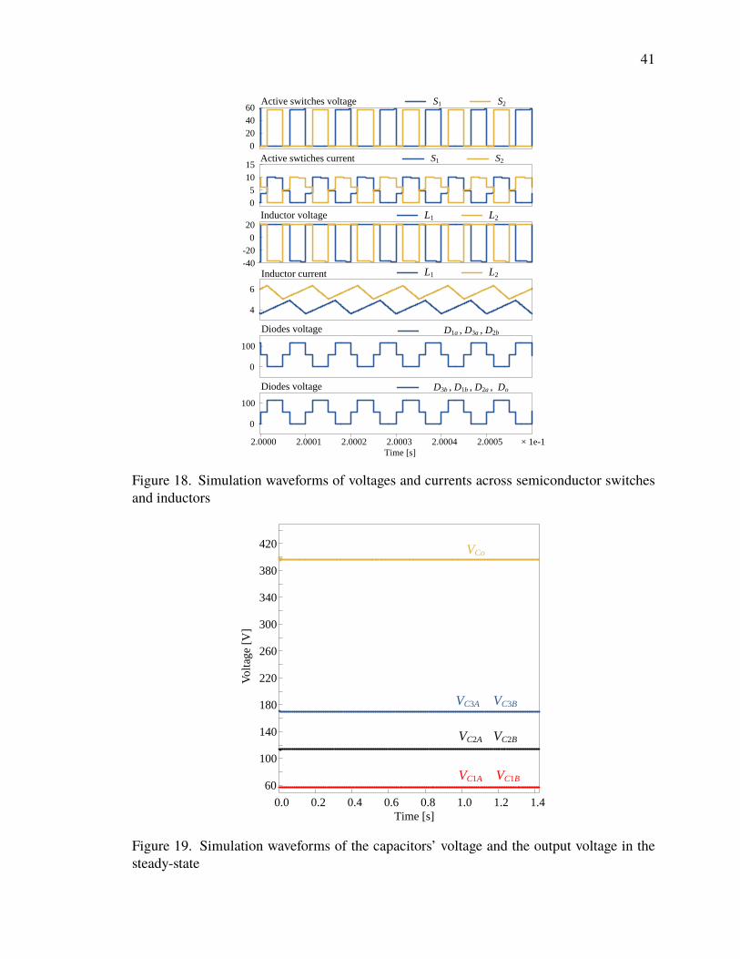
41
0
20
40
60
0
5
10
15
-40
-20
0
20
4
6
0
100
0
100
× 1e-1
Time [s]
2.0000 2.0001 2.0002 2.0003 2.0004 2.0005
Diodes voltage D3b , D1b , D2a , Do
Diodes voltage D1a , D3a , D2b
Inductor voltage
Inductor current
L1 L2
L1 L2
Active switches voltage
Active swtiches current
S1 S2
S1 S2
Figure 18. Simulation waveforms of voltages and currents across semiconductor switchesand inductors
Time [s]
0.0 0.2 0.4 0.6 0.8 1.0 1.2 1.4
Volt
age
[V]
60
100
140
180
220
260
300
340
380
420
VC1A VC1B
VC3A VC3B
VCo
VC2A VC2B
Figure 19. Simulation waveforms of the capacitors’ voltage and the output voltage in thesteady-state
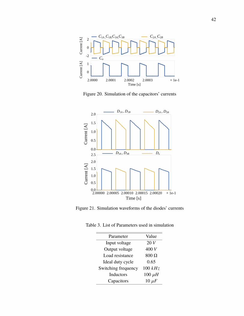
42
-2
0
2
× 1e-1
Time [s]
2.0000 2.0001 2.0002 2.0003
0
1
Cu
rren
t [A
]C
urr
ent
[A] C1A ,C1B,C3A,C3B C2A ,C2B
Co
Figure 20. Simulation of the capacitors’ currents
0.0
0.5
1.0
1.5
2.0
× 1e-1
Time [s]
2.00000 2.00005 2.00010 2.00015 2.000200.0
0.5
1.0
1.5
2.0
2.5D3A , D3B Do
D1A , D1B D2A , D2B
Curr
ent
[A]
Cu
rren
t [A
]
Figure 21. Simulation waveforms of the diodes’ currents
Table 3. List of Parameters used in simulation
Parameter ValueInput voltage 20 VOutput voltage 400 VLoad resistance 800 ΩIdeal duty cycle 0.65
Switching frequency 100 kHzInductors 100 µHCapacitors 10 µF

43
Power [W]
0 20 40 60 80 100 120 140 160 180 2000
10
20
30
40
50
60
70
80
90
100
Power [W]
0 20 40 60 80 100 120 140 160 180 2000
0.5
1
1.5
2
2.5
3
3.5
4
4.5
5
MOSFETs Conduction MOSFETs Switching Diodes Inductors Capacitors
Per
cen
tage
[%]
Pow
er l
oss
[W
]
Figure 22. Efficiency analysis of the example converter; the actual losses (left) and the lossbreakdown (right)
wires. The AFG3052C signal generator was used to generate gate signals with a switching
frequency of 50 kHz. The converter is fed by 20 V , where N5700 power supply is used, and
the output load is implemented using ceramic resistors with various values. The voltage
stress across the active switches and diodes are shown in Figure 24, which supports the
simulation results as the voltage across the active switches equals 57 V , and the maximum
voltage stress across the diodes equals 124 V . The voltage across the capacitors is shown
in Figure 25. The voltage across each capacitor in the first stage equals 57 V , in the second
stage equals 133 V , and in the third stage equals 200 V . The output voltage equals 400 V .
The current waveforms of inductors, switches, and capacitors were acquired at ≈ 100 W ,
as shown in Figure 26 and 27. The peak efficiency of the converter is about 97% at 160 W
and about 96.3% at 200 W .

44
Signal generator
The hardware
prototype
The load
Oscilloscope Auxiliary
supply
The proposed
converter
Signal generator
Measurement devices
VDC
Ceramic
resistors
Figure 23. The hardware prototype and the experimental setup
Table 4. List of Components used for the hardware prototype
Item Designation Rating Part No.
Inductor L1, L2 100 µH, DCR = 25 mΩ, 60B104C
CapacitorC1A,C2AC1BC2BC3AC3B
10 µF B32674D3106K
Capacitor Co 22 µF B32774D4226K000
MOSFET Q1,Q2150 V,37 A
Rds(on) = 10.525 mΩ IPA105N15N3
Diode D1A,D2AD1B,D2B
250V,40AVF = 0.86 V, trr = 35 ns MBR40250G
load Rload multiple values L100J100E, L225J50REL225J250E,L225J500E
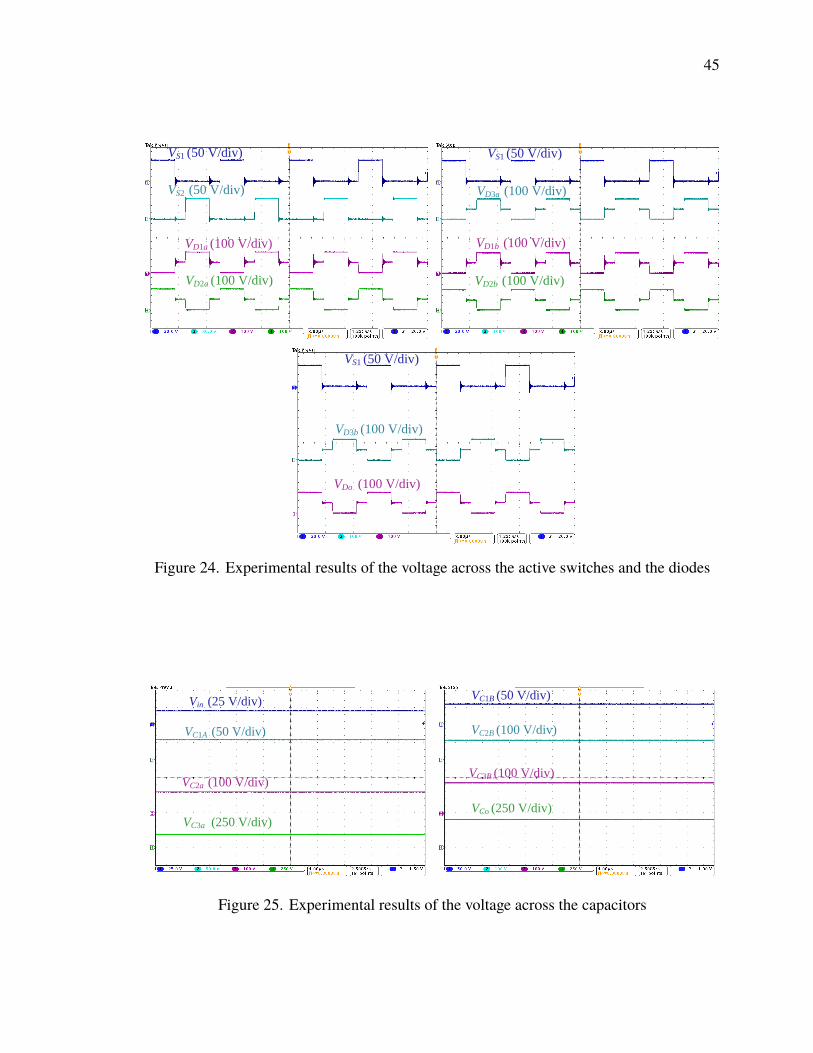
45
VS1 (50 V/div)
VS2 (50 V/div)
VD1a (100 V/div)
VD2a (100 V/div)
VD3a (100 V/div)
VD1b (100 V/div)
VD2b (100 V/div)
VS1 (50 V/div)
VD3b (100 V/div)
VDo (100 V/div)
VS1 (50 V/div)
Figure 24. Experimental results of the voltage across the active switches and the diodes
Vin (25 V/div)
VC1A (50 V/div)
VC2a (100 V/div)
VC3a (250 V/div)
VC2B (100 V/div)
VC3B (100 V/div)
VCo (250 V/div)
VC1B (50 V/div)
Figure 25. Experimental results of the voltage across the capacitors
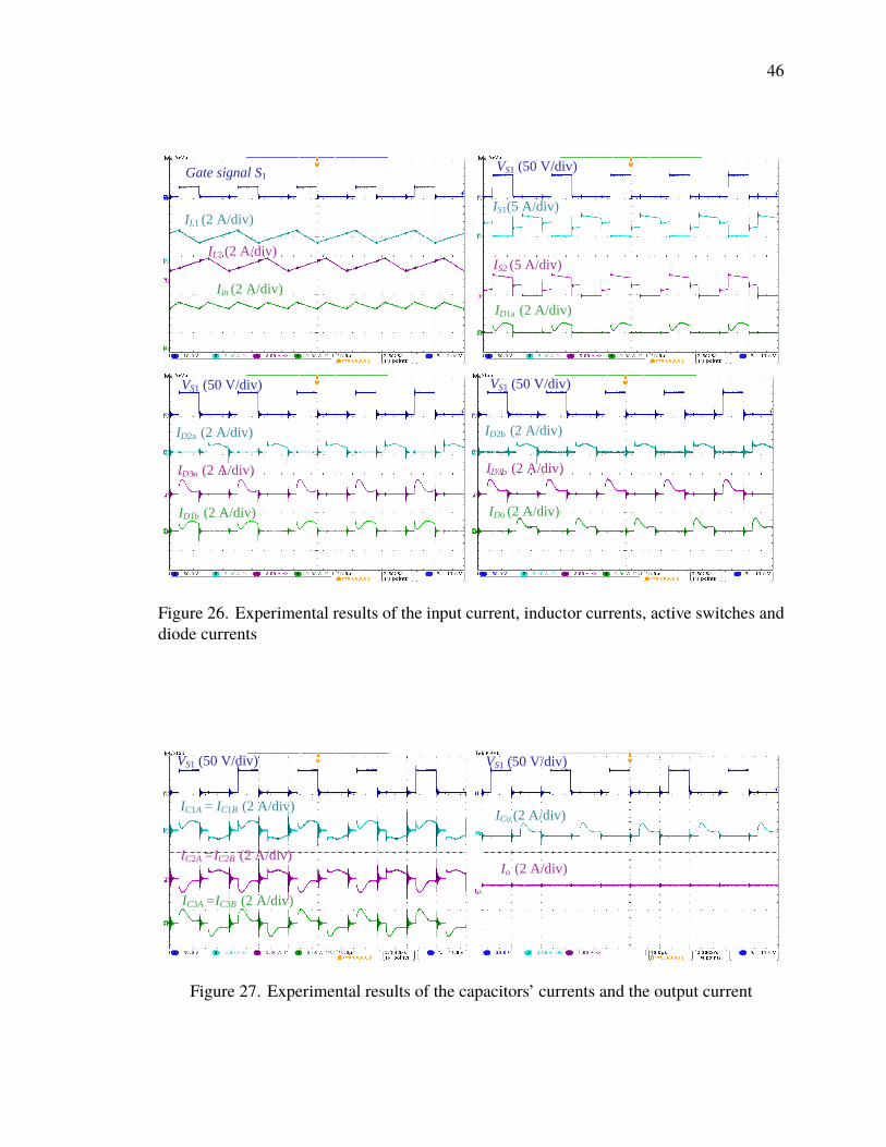
46
IL1 (2 A/div)
IL2 (2 A/div)
Iin (2 A/div)
IS1(5 A/div)
IS2 (5 A/div)
ID1a (2 A/div)
VS1 (50 V/div)
ID2a (2 A/div)
ID3a (2 A/div)
ID1b (2 A/div) IDo (2 A/div)
Gate signal S1
VS1 (50 V/div) VS1 (50 V/div)
ID2b (2 A/div)
ID3b (2 A/div)
Figure 26. Experimental results of the input current, inductor currents, active switches anddiode currents
IC1A = IC1B (2 A/div)
IC2A =IC2B (2 A/div)
ICo (2 A/div)
Io (2 A/div)
IC3A =IC3B (2 A/div)
VS1 (50 V/div) VS1 (50 V/div)
Figure 27. Experimental results of the capacitors’ currents and the output current
47
8. CONCLUSION
In this paper, the family of an interleaved boost converter with voltage multiplier
cells was presented. The general structure of the family consists of two sections: an
interleaved boost stage and voltage multiplier cells. The structure comes in two configu-
rations. Configuration 1’s output is filtered using an output diode and a capacitor filter,
where configuration 2’s output is filtered using an LC filter. The difference between the two
configurations was explained, and a comparison between the various family members was
presented. An example of this family was given with a detailed steady-state analysis and
component selection, which was evinced by simulation. A 200-W hardware prototype was
implemented to further verify the analysis and the simulation. The converter is capable of
drawing power from both a single or dual independent input voltage and with the same or
different duty cycles of the active switches. These cases were summarized and compared.
The family has good features besides the high-voltage gain. The input current ripple has
twice frequency of the one in the conventional boost converter, which reduces the filter
requirements and increases the accuracy of the current sensing for better tracking of MPPT.
Although the converter is efficient, the efficiency can be further increased by either replacing
the diodes with better ones or with active switches, with a trade-off of the complexity.
REFERENCES
[1] R. Teodorescu, M. Liserre, and P. Rodriguez, Grid converters for photovoltaic andwind power systems. John Wiley & Sons, 2011, vol. 29.
[2] F. Blaabjerg, Y. Yang, and K. Ma, “Power electronics - key technology for renewableenergy systems - status and future,” in 2013 3rd International Conference on ElectricPower and Energy Conversion Systems, Oct 2013, pp. 1–6.
[3] J. W. Kolar, J. Biela, S. Waffler, T. Friedli, and U. Badstübner, “Performance trendsand limitations of power electronic systems,” in Integrated Power Electronics Systems(CIPS), 2010 6th International Conference on. IEEE, 2010, pp. 1–20.
48
[4] J. D. van Wyk and F. C. Lee, “On a future for power electronics,” IEEE Journal ofEmerging and Selected Topics in Power Electronics, vol. 1, no. 2, pp. 59–72, 2013.
[5] V. A. K. Prabhala, B. P. Baddipadiga, and M. Ferdowsi, “Dc distribution systems;an overview,” in 2014 International Conference on Renewable Energy Research andApplication (ICRERA), Oct 2014, pp. 307–312.
[6] A. Pratt, P. Kumar, and T. V. Aldridge, “Evaluation of 400v dc distribution in telcoand data centers to improve energy efficiency,” in INTELEC 07 - 29th InternationalTelecommunications Energy Conference, Sept 2007, pp. 32–39.
[7] P. T. Krein, “Data center challenges and their power electronics,” CPSS Transactionson Power Electronics and Applications, vol. 2, no. 1, pp. 39–46, 2017.
[8] D. J. Hammerstrom, “Ac versus dc distribution systemsdid we get it right?” in 2007IEEE Power Engineering Society General Meeting, June 2007, pp. 1–5.
[9] A.Mohamed andO.Mohammed, “Connectivity of dcmicrogrids involving sustainableenergy sources,” in 2011 IEEE Industry Applications Society Annual Meeting, Oct2011, pp. 1–8.
[10] V.A.K. Prabhala, P. Fajri, V. S. P. Gouribhatla, B. P. Baddipadiga, andM. Ferdowsi, “Adc–dc converter with high voltage gain and two input boost stages,” IEEE Transactionson Power Electronics, vol. 31, no. 6, pp. 4206–4215, 2016.
[11] R.-J. Wai, C.-Y. Lin, R.-Y. Duan, and Y.-R. Chang, “High-efficiency dc-dc converterwith high voltage gain and reduced switch stress,” IEEE Transactions on IndustrialElectronics, vol. 54, no. 1, pp. 354–364, 2007.
[12] L.-S. Yang, T.-J. Liang, and J.-F. Chen, “Transformerless dc–dc converters with highstep-up voltage gain,” IEEE Transactions on Industrial Electronics, vol. 56, no. 8, pp.3144–3152, 2009.
[13] Q. Zhao and F. C. Lee, “High-efficiency, high step-up dc-dc converters,” IEEE Trans-actions on Power Electronics, vol. 18, no. 1, pp. 65–73, 2003.
[14] S.-M. Chen, T.-J. Liang, L.-S. Yang, and J.-F. Chen, “A cascaded high step-up dc–dc converter with single switch for microsource applications,” IEEE Transactions onPower Electronics, vol. 26, no. 4, pp. 1146–1153, 2011.
[15] N.Denniston, A.M.Massoud, S.Ahmed, andP.N. Enjeti, “Multiple-module high-gainhigh-voltage dc–dc transformers for offshorewind energy systems,” IEEETransactionson Industrial Electronics, vol. 58, no. 5, pp. 1877–1886, 2011.
[16] Z. Liang, R. Guo, J. Li, and A. Q. Huang, “A high-efficiency pv module-integrateddc/dc converter for pv energy harvest in freedm systems,” IEEE Transactions on PowerElectronics, vol. 26, no. 3, pp. 897–909, 2011.
49
[17] B. Axelrod, Y. Berkovich, and A. Ioinovici, “Transformerless dc-dc converters witha very high dc line-to-load voltage ratio,” in Circuits and Systems, 2003. ISCAS’03.Proceedings of the 2003 International Symposium on, vol. 3. IEEE, 2003, pp. III–III.
[18] S. Dwari and L. Parsa, “An efficient high-step-up interleaved dc–dc converter with acommon active clamp,” IEEE Transactions on Power Electronics, vol. 26, no. 1, pp.66–78, 2011.
[19] T.-F. Wu, Y.-C. Chen, J.-G. Yang, and C.-L. Kuo, “Isolated bidirectional full-bridgedc–dc converter with a flyback snubber,” IEEE Transactions on Power Electronics,vol. 25, no. 7, pp. 1915–1922, 2010.
[20] F. S. Silva, A. A. Freitas, S. Daher, S. C. Ximenes, S. K. Sousa, M. Edilson, F. L.Antunes, and C. M. Cruz, “High gain dc-dc boost converter with a coupling inductor,”in Power Electronics Conference, 2009. COBEP’09. Brazilian. IEEE, 2009, pp.486–492.
[21] V. Yaramasu and B.Wu, “Three-level boost converter basedmedium voltagemegawattpmsg wind energy conversion systems,” in Energy Conversion Congress and Exposi-tion (ECCE), 2011 IEEE. IEEE, 2011, pp. 561–567.
[22] J.-M. Kwon, B.-H. Kwon, and K.-H. Nam, “Three-phase photovoltaic system withthree-level boosting mppt control,” IEEE Transactions on Power Electronics, vol. 23,no. 5, pp. 2319–2327, 2008.
[23] R. W. Erickson and D. Maksimovic, Fundamentals of power electronics. SpringerScience & Business Media, 2007.
[24] F. L. Tofoli, D. de Souza Oliveira, R. P. Torrico-Bascopé, and Y. J. A. Alcazar,“Novel nonisolated high-voltage gain dc-dc converters based on 3ssc and vmc,” IEEETransactions on Power Electronics, vol. 27, no. 9, pp. 3897–3907, Sept 2012.
[25] F. L. Tofoli, D. d. C. Pereira, W. J. de Paula, and D. d. S. Oliveira Júnior, “Survey onnon-isolated high-voltage step-up dc-dc topologies based on the boost converter,” IETPower Electronics, vol. 8, no. 10, pp. 2044–2057, 2015.
[26] R. Haroun, A. E. Aroudi, A. Cid-Pastor, G. Garcia, C. Olalla, and L. Martínez-Salamero, “Impedance matching in photovoltaic systems using cascaded boost con-verters and sliding-mode control,” IEEE Transactions on Power Electronics, vol. 30,no. 6, pp. 3185–3199, June 2015.
[27] M. Veerachary and S. B. Sudhakar, “Stability analysis of cascaded dc-dc power elec-tronic system,” in 2007 7th International Conference on Power Electronics and DriveSystems, Nov 2007, pp. 1422–1426.
[28] M. T. V. and I. Barbi, “Nonisolated high step-up stacked dc-dc converter based onboost converter elements for high power application,” in 2011 IEEE InternationalSymposium of Circuits and Systems (ISCAS), May 2011, pp. 249–252.
50
[29] M. Forouzesh, Y. P. Siwakoti, S. A. Gorji, F. Blaabjerg, and B. Lehman, “Step-up dc-dc converters: A comprehensive review of voltage-boosting techniques, topologies,and applications,” IEEE Transactions on Power Electronics, vol. 32, no. 12, pp. 9143–9178, Dec 2017.
[30] B. P. R. Baddipadiga, V. A. Prabhala, and M. Ferdowsi, “A family of high-voltage-gain dc-dc converters based on a generalized structure,” IEEE Transactions on PowerElectronics, vol. PP, no. 99, pp. 1–1, 2017.
[31] R. Gules, L. L. Pfitscher, and L. C. Franco, “An interleaved boost dc-dc converterwith large conversion ratio,” in 2003 IEEE International Symposium on IndustrialElectronics ( Cat. No.03TH8692), vol. 1, June 2003, pp. 411–416 vol. 1.
[32] C.-M. Lai, Y.-C. Lin, and D. Lee, “Study and implementation of a two-phase inter-leaved bidirectional dc/dc converter for vehicle and dc-microgrid systems,” Energies,vol. 8, no. 9, pp. 9969–9991, 2015.
[33] M. Prudente, L. L. Pfitscher, G. Emmendoerfer, E. F. Romaneli, andR.Gules, “Voltagemultiplier cells applied to non-isolated dc–dc converters,” IEEETransactions onPowerElectronics, vol. 23, no. 2, pp. 871–887, March 2008.
[34] W. Li, Y. Zhao, Y. Deng, and X. He, “Interleaved converter with voltage multipliercell for high step-up and high-efficiency conversion,” IEEE Transactions on PowerElectronics, vol. 25, no. 9, pp. 2397–2408, 2010.
[35] P. Kim, S. Lee, J. Park, and S. Choi, “High step-up interleaved boost converters usingvoltage multiplier cells,” in Power Electronics and ECCE Asia (ICPE and ECCE),2011 IEEE 8th International Conference on. IEEE, 2011, pp. 2844–2851.
[36] W. Li and X. He, “Review of nonisolated high-step-up dc/dc converters in photovoltaicgrid-connected applications,” IEEE Transactions on Industrial Electronics, vol. 58,no. 4, pp. 1239–1250, April 2011.
[37] L. Zhou, B. Zhu, Q. Luo, and S. Chen, “Interleaved non-isolated high step-up dc/dcconverter based on the diode-capacitor multiplier,” IET Power Electronics, vol. 7,no. 2, pp. 390–397, February 2014.
[38] M. O’Loughlin, “An interleaving pfc pre-regulator for high-power converters,” TexasInstruments, pp. 1–14, 2006.
[39] J. Roy and R. Ayyanar, “Sensor-less current sharing over wide operating rangefor extended-duty-ratio boost converter,” IEEE Transactions on Power Electronics,vol. 32, no. 11, pp. 8763–8777, Nov 2017.
[40] T. Nouri, S. H. Hosseini, E. Babaei, and J. Ebrahimi, “Generalised transformerlessultra step-up dc–dc converter with reduced voltage stress on semiconductors,” IETPower Electronics, vol. 7, no. 11, pp. 2791–2805, 2014.

51
[41] E. H. Ismail, M. A. Al-Saffar, and A. J. Sabzali, “High conversion ratio dc–dc convert-ers with reduced switch stress,” IEEE Transactions on Circuits and Systems I: RegularPapers, vol. 55, no. 7, pp. 2139–2151, Aug 2008.
[42] J. C. Rosas-Caro, J. C. Mayo-Maldonado, R. Salas-Cabrera, A. Gonzalez-Rodriguez,E. N. Salas-Cabrera, and R. Castillo-Ibarra, “A family of dc-dc multiplier converters,”Engineering Letters, vol. 19, no. 1, pp. 57–67, 2011.
[43] Y. J. A. Alcazar, D. de Souza Oliveira, F. L. Tofoli, and R. P. Torrico-Bascopé,“Dc–dc nonisolated boost converter based on the three-state switching cell and voltagemultiplier cells,” IEEE Transactions on Industrial Electronics, vol. 60, no. 10, pp.4438–4449, Oct 2013.
[44] M. A. Al-Saffar and E. H. Ismail, “A high voltage ratio and low stress dc–dc converterwith reduced input current ripple for fuel cell source,” Renewable Energy, vol. 82, pp.35–43, 2015.
[45] A. A. Fardoun, E. H. Ismail, A. J. Sabzali, and M. A. Al-Saffar, “Bidirectionalconverter for high-efficiency fuel cell powertrain,” Journal of Power Sources, vol.249, pp. 470–482, 2014.
[46] A. Alzahrani, P. Shamsi, and M. Ferdowsi, “A novel non-isolated high-gain dc-dcboost converter,” in 2017 North American Power Symposium (NAPS), Sept 2017, pp.1–6.
[47] A. Alzahrani, P. Shamsi, and M. Ferdowsi, “An interleaved non-isolated dc-dc boostconverter with diode-capacitor cells,” in 2017 IEEE 6th International Conference onRenewable Energy Research and Applications (ICRERA), Nov 2017, pp. 216–221.
[48] L. Müller and J. W. Kimball, “High gain dc–dc converter based on the cockcroft–walton multiplier,” IEEE Transactions on Power Electronics, vol. 31, no. 9, pp. 6405–6415, 2016.
[49] B. P. Baddipadiga and M. Ferdowsi, “A high-voltage-gain dc-dc converter basedon modified dickson charge pump voltage multiplier,” IEEE Transactions on PowerElectronics, vol. 32, no. 10, pp. 7707–7715, Oct 2017.
52
II. HIGH-VOLTAGE-GAIN DC-DC STEP-UP CONVERTERWITH BI-FOLDDICKSON VOLTAGE MULTIPLIER CELLS
Ahmad Alzahrani, Pourya Shamsi, and Mehdi Ferdowsi
Departement of Electrical and Computer Engineering
Missouri University of Science and Technology
asakw9, shamsip, [email protected]
ABSTRACT
This paper presents an interleaved boost converter with a bi-fold Dickson voltage
multiplier suitable for interfacing low-voltage renewable energy sources to high-voltage
distribution buses and other applications that require a high-voltage-gain conversion ratio.
The proposed converter was constructed from two stages: an interleaved boost stage, which
contains two inductors operated by two low-side active switches, and a voltage multiplier
cell (VMC) stage, which mainly consists of diodes and capacitors to increase the overall
voltage gain. The proposed converter offers a high-voltage-gain ratio with low voltage
stress on the semiconductor switches as well as the passive components. This allows the
selection of efficient and compact components. Moreover, the required inductance that
ensures operation in the continuous conduction mode (CCM) is lower than the one in the
conventional interleaved boost converter. The distinction of the proposed converter is that
the inductors’ currents are equal, regardless of the number of VMCs. Equal sharing of
interleaved boost-stage currents reduces the conduction loss in the active switches as well
as the inductors and thus improves the overall efficiency, as the conduction power loss is a
quadratic function. In this paper, the theory of operation and steady-state analysis of the
proposed converter are illustrated and verified by simulation results. A 200 W hardware
prototype was implemented to convert a 20 V to a 400 V DC load and validate both the
theory and the simulation.

53
Keywords: High-Gain, bi-fold Dickson, DC-DC, VMC, Renewable, PV, Solar, MPPT
1. INTRODUCTION
Step-up DC-DC converters with high-voltage-gain ratios were only used in a limited
number of applications, such as radar and X-ray systems. Currently, they are being used in
a wide variety of applications such as photovoltaic (PV) panels’ interface to a microgrid or
a DC distribution bus, as shown in Figure 1(a), or power distribution unit (PDU) to power
data centers and supercomputers [1], as shown in Figure 1(b). Both applications deploy a
400 VDC distribution system due to its advantage over an AC distribution system in terms
of the number of conversion units, size, cost, and immunity against load disturbances and
ground faults [2–6]. Most PV panels have an output voltage range between 15 and 45 V [7],
which is very low. Integrating a PV panel to a 400 VDC is a challenging task and necessitates
a high-voltage-gain step-up converter.
The conventional boost converter (CBC) requires operation at very high duty cycles
to obtain a high-voltage-gain ratio. In practice, the gain of the CBC is limited by the
conduction losses, and obtaining a high-voltage-gain ratio is not feasible. Not only that,
but the CBC also suffers from the voltage stress and reverse recovery phenomenon at high
voltages [8] and requires a large inductor to operate in the CCM. Derived topologies from
the CBC, such as cascaded boost converters, can achieve a higher voltage and operate
at low duty cycles [9, 10]. However, they suffer from low efficiency due to the power
being processed multiple times and require complicated control and extra effort to ensure
stability [11, 12]. The three-level boost converter is derived from the series-input series-
output multiphase boost converter. The stress on the switches and inductance requirement is
reduced. However, it still has the same gain as theCBC [13–15]. The single-switch quadratic
boost converter has a simple structure and does not suffer from instability like the cascaded
boost converter. However, the voltage and current stress across the switches are high, and
the inductor that ensures the CCM operation is large. Using isolated topologies such as
54
forward, flyback, or full-bridge converters, the high-voltage-gain ratio at can be achieved
lower duty cycles by increasing the turns ratio of the transformer [16–18]. However, such
devices suffer from parasitic leakage inductance, which significantly increases the voltage
stress on the active switches and can cause damage unless additional auxiliary is used [19].
Isolated converters generally have low power density, higher cost, and lower efficiency than
non-isolated converters [20–22].
Using VMCwith the CBC increases the voltage gain and improves the performance,
as the total indirect power is reduced [23, 24]. Nevertheless, the inductor size is still
relatively substantial to obtain a smooth input current. Therefore, topologies such as those
found in [25, 26] use VMCs with an interleaved boost stage to reduce the magnetic storage
requirement and obtain a smoother input current. The stress on the internal components
depends on the VMC connections and the number of cells (e.g., the modified Dickson cell
has lower voltage stress across the components than the original Dickson cell). This paper
presents a high-gain interleaved DC-DC converter that is an improved version of [25, 26].
The features of the proposed converter can be summarized as follows: 1- The converter has
a high-voltage-gain ratio that is sufficient for the integration of renewable energy sources to
a high voltage DC bus. 2- The voltage stresses across active switches, diodes, and passive
components are low, and that allows the selection of components whose cost, efficiency, and
compactness are balanced. 3- The input current is shared equally between the two phases,
regardless of the number of VMC stages. Therefore, the conduction loss of the interleaved
boost stage and the thermal dissipation requirement are reduced. 4- The converter has two
capacitors at each stage, in which voltage ripple cancellation is achieved. 5- The input
current is continuous and has low ripple due to the interleaving. Hence, continuity of the
input current reduces the filter requirement and allows accurate current measurement for
maximum power point tracking (MPPT). 6- The converter does not need an output diode
or an LC filter to rectify or regulate the output voltage such as in [25, 26]. Each stage can
produce a constant DC voltage.

55
Figure 1. Application of a high-gain DC-DC converter
The rest of this paper is structured as follows. First, the construction of the bi-fold
Dickson cell and the Dickson voltage multiplier is presented and explained in Section 2.
The theory of operation and a comparison to similar converters is illustrated in Section
3. The analysis of CCM modes and steady-state voltage gain formulas are derived in
Section 4. Section 5 presents the operation of the converter in the discontinuous conduction
mode and the boundary conduction mode The component selections and their power loss
models are derived in Section 6, and the simulation results are presented in Section 7. The
implementation of the hardware prototype and the experimental results are explained in
Section 8. Finally, conclusions and future work are presented in Section 9.
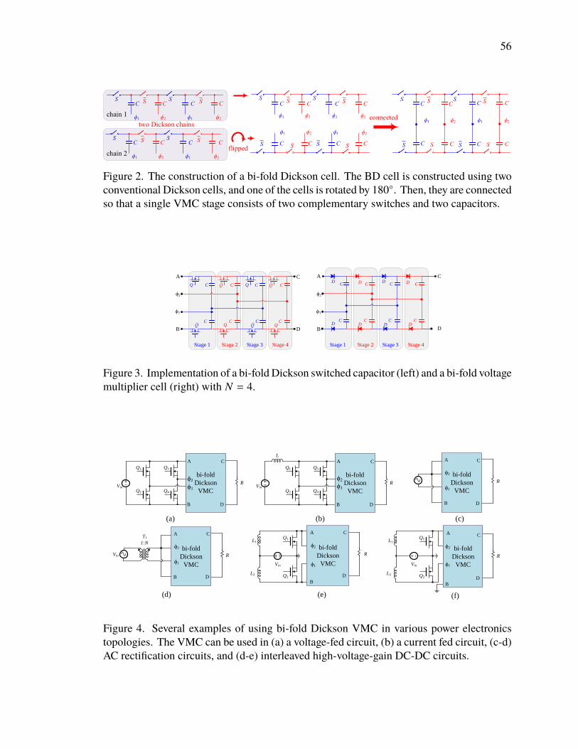
56
ϕ1
flipped
ϕ2 ϕ1 ϕ2ϕ1 ϕ2 ϕ1 ϕ2
ϕ1 ϕ2 ϕ1 ϕ2
ϕ1 ϕ2 ϕ1 ϕ2connected
C C C C C C C C
C C C C
S S S S S S
SS
C C C C
C C C C SS
S S S S S S
S SS S
ϕ1 ϕ2 ϕ1 ϕ2
C C C CS SS S
two Dickson chains
chain 1
chain 2
Figure 2. The construction of a bi-fold Dickson cell. The BD cell is constructed using twoconventional Dickson cells, and one of the cells is rotated by 180. Then, they are connectedso that a single VMC stage consists of two complementary switches and two capacitors.
Q Q Q Q
Q Q Q Q
C C C C
C C C C
C C C C
C C C C
D
D
D
D
D
D
A A
ϕ2
B
ϕ1
ϕ2
B
ϕ1
C
D
C
DD
D
Stage 1 Stage 2 Stage 3 Stage 4 Stage 1 Stage 2 Stage 3 Stage 4
Figure 3. Implementation of a bi-fold Dickson switched capacitor (left) and a bi-fold voltagemultiplier cell (right) with N = 4.
Q1
Q2
Q3
Q4
bi-fold
Dickson
VMC
R
A
ϕ2
B D
C
ϕ1Vin
Q1
Q2
Q3
Q4
bi-fold
Dickson
VMC
R
A
ϕ2
B D
C
ϕ1Vin
L
R
bi-fold
Dickson
VMC
A
ϕ2
B
ϕ1
R
bi-fold
Dickson
VMC
A
ϕ2
B
ϕ1
L1Q1
Q2L2
bi-fold
Dickson
VMC
A
ϕ2
B
ϕ1Vin
L1Q1
Q2L2
bi-fold
Dickson
VMC
A
ϕ2
B
ϕ1Vin
D
C
D
C
D
C
R
D
C
RVin
1:N
T1
(a) (b)
(d) (e)
(c)
(f)
Figure 4. Several examples of using bi-fold Dickson VMC in various power electronicstopologies. The VMC can be used in (a) a voltage-fed circuit, (b) a current fed circuit, (c-d)AC rectification circuits, and (d-e) interleaved high-voltage-gain DC-DC circuits.

57
2. CONSTRUCTION OF BI-FOLD DICKSON SC/VMCS
The conventional Dickson charge pump or voltage multiplier is shown in Figure 2.
The circuit takes a DC input voltage and converts it to high-level voltage by charging and
discharging internal capacitors. It has been utilized in a variety of applications, including
nonvolatile memories, RF antenna switched controllers [27], and recently it was used for
ultra step-up voltage ratio converters [26]. The challenge with a Dickson voltage multiplier
is that the stress across the capacitors increases as the number of stages increases. Although
multiple capacitors can be connected in a series to satisfy the voltage rating, voltage
mismatches between capacitors might appear. One way to remove the mismatches is by
connecting a resistance in parallel with the capacitors. That makes the resistance dissipate
the excessive power. However, this method might not work in high power applications
because of the high power dissipation and thermal limitations. Therefore, this paper
introduces a bi-fold Dickson voltage multiplier to reduce the voltage stresses on both
semiconductors and capacitors. The construction of the bi-fold Dickson cell is shown in
Figure 2. The cell is constructed by using two traditional Dickson cells and rotating one
by 180. Then, the capacitors of the upper cell are connected to the capacitors of the lower
cell. That is, phase φ1 of the upper cell is connected to φ1 in the lower cell, and likewise for
the capacitors connected to phase φ2. The proposed cell consists of multiple stages; each
stage has two complementary switches and two capacitors. Either active switches or diodes
can be used to implement the switches in the proposed cell, as shown in Figure 3. This
can be seen as a trade-off between efficiency, cost, and control complexity. If the switches
were implemented using diodes, the forward voltage of the diodes would compromise the
overall efficiency. However, with using diodes, the converter has spontaneous split-phase
control [28]. The diodes remain reverse-biased until the voltage mismatches between the
capacitors are gone. Therefore, no current spikes are present. Alternately, if the switches
are implemented using active switches, the efficiency can be significantly improved, but
complex control is needed. That is, the switches must be delayed to prevent temporary
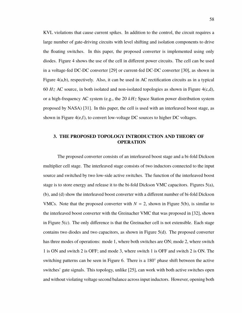
58
KVL violations that cause current spikes. In addition to the control, the circuit requires a
large number of gate-driving circuits with level shifting and isolation components to drive
the floating switches. In this paper, the proposed converter is implemented using only
diodes. Figure 4 shows the use of the cell in different power circuits. The cell can be used
in a voltage-fed DC-DC converter [29] or current-fed DC-DC converter [30], as shown in
Figure 4(a,b), respectively. Also, it can be used in AC rectification circuits as in a typical
60 Hz AC source, in both isolated and non-isolated topologies as shown in Figure 4(c,d),
or a high-frequency AC system (e.g., the 20 kHz Space Station power distribution system
proposed by NASA) [31]. In this paper, the cell is used with an interleaved boost stage, as
shown in Figure 4(e,f), to convert low-voltage DC sources to higher DC voltages.
3. THE PROPOSED TOPOLOGY INTRODUCTION AND THEORY OFOPERATION
The proposed converter consists of an interleaved boost stage and a bi-fold Dickson
multiplier cell stage. The interleaved stage consists of two inductors connected to the input
source and switched by two low-side active switches. The function of the interleaved boost
stage is to store energy and release it to the bi-fold Dickson VMC capacitors. Figures 5(a),
(b), and (d) show the interleaved boost converter with a different number of bi-fold Dickson
VMCs. Note that the proposed converter with N = 2, shown in Figure 5(b), is similar to
the interleaved boost converter with the Greinacher VMC that was proposed in [32], shown
in Figure 5(c). The only difference is that the Greinacher cell is not extensible. Each stage
contains two diodes and two capacitors, as shown in Figure 5(d). The proposed converter
has three modes of operations: mode 1, where both switches are ON; mode 2, where switch
1 is ON and switch 2 is OFF; and mode 3, where switch 1 is OFF and switch 2 is ON. The
switching patterns can be seen in Figure 6. There is a 180 phase shift between the active
switches’ gate signals. This topology, unlike [25], can work with both active switches open
andwithout violating voltage second balance across input inductors. However, opening both

59
active switches creates several drawbacks to the interleaved topology, such as a reduction in
the voltage gain and an imbalance between capacitor voltage. Therefore, it is not beneficial to
use this topology for a duty cycle less than 50%. To conduct the analysis, a few assumptions
are considered: 1) All components of the proposed converter are ideal; 2) The capacitors
are large enough that the voltage ripples can be neglected; 3) The converter operates in the
steady state; 4) The duty cycles are symmetrical and greater than 50%, and the converter is
fed by a single voltage source. Nonetheless, the voltage gain ratio of the proposed converter
will be summarized for cases where the duty cycles are asymmetrical and for cases where
the converter is fed by two independent voltage sources.
4. MODE ANALYSIS AND STEADY STATE VOLTAGE GAIN
4.1. MODE 1 (T0 − T1) AND (T2 − T3) : BOTH Q1 AND Q2 ARE ON
In this mode, both active switches are conducting and allowing the source to transfer
energy to both inductors. All diodes are reverse-biased, and they are OFF. The equivalent
circuit of this mode is shown in Figure 7(a). The last-stage capacitors, C3A and C3B keep
the energy level to the output load. The state equations of this mode are given by
L1diL1
dt= vL1 = Vin (1)
L2diL2
dt= vL2 = Vin (2)
4.2. MODE 2 (T1 − T2): Q1 IS ON AND Q2 IS OFF
In this mode, Q1 is still ON, and L1 keeps drawing energy from the source. Alter-
nately, Q2 is turned OFF, and the energy in L2 is released to the VMC stage. Diodes D1B ,
D2A, and D3B are forward-biased andON,while diodes D1A,D2B , and D3A are reverse-biased
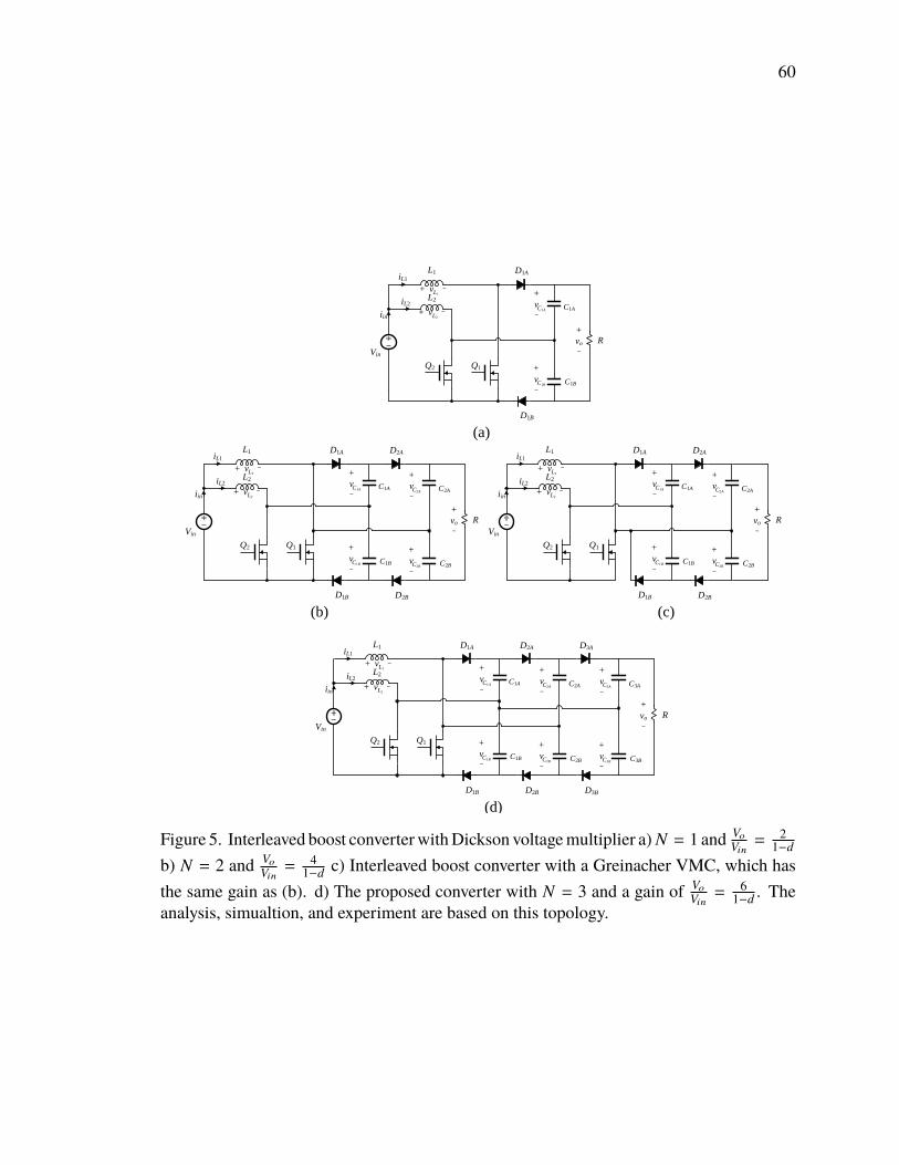
60
R
C1A
+
v _
C1A
C1B
+
v _
C1B
D1A
D1B
+
vo _
Vin
L1
Q1Q2
L2
(a)
iin
iL1
iL2
L1 + v _
+ v _L2
R
C2A
+
v _
C2A
C2B
+
v _
C2B
C1A
+
v _
C1A
C1B
+
v _
C1B
D1A D2A
D1B D2B
+
vo _Vin
L1
Q1Q2
L2
(b)
iin
iL1
iL2
L1 + v
_
+ v _
L2
C3A
+
v _
R
C3A
C3B
+
v _
C3B
C2A
+
v _
C2A
C2B
+
v _
C2B
C1A
+
v _
C1A
C1B
+
v _
C1B
D1A D2A D3A
D1B D2B D3B
+
vo _Vin
L1
Q1Q2
L2
(d)
iin
iL1
iL2
L1 + v _
+ v _L2
R
C2A
+
v _
C2A
C2B
+
v _
C2B
C1A
+
v _
C1A
C1B
+
v _
C1B
D1A D2A
D1B D2B
+
vo _Vin
L1
Q1Q2
L2
(c)
iin
iL1
iL2
L1 + v
_
+ v _
L2
Figure 5. Interleaved boost converterwithDickson voltagemultiplier a) N = 1 and Vo
Vin= 2
1−d
b) N = 2 and Vo
Vin= 4
1−d c) Interleaved boost converter with a Greinacher VMC, which hasthe same gain as (b). d) The proposed converter with N = 3 and a gain of Vo
Vin= 6
1−d . Theanalysis, simualtion, and experiment are based on this topology.
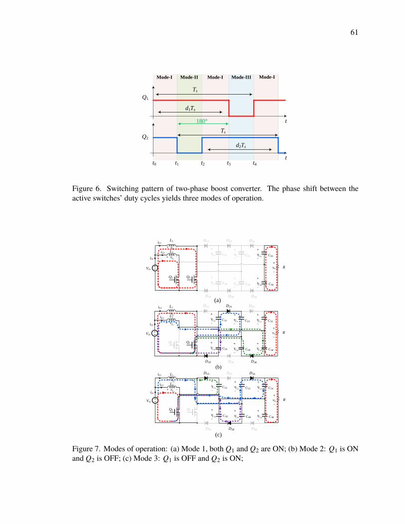
61
Mode-I
Q1
Q2
Mode-I Mode-II Mode-III
t
t
Ts
Ts
d2Ts
d1Ts
Mode-I
t0 t1 t2 t3 t4
180°
Figure 6. Switching pattern of two-phase boost converter. The phase shift between theactive switches’ duty cycles yields three modes of operation.
C3A
+
v _
R
C3A
C3B
+
v _
C3B
C2A
+
v _
C2A
C2B
+
v _
C2B
C1A
+
v _
C1A
C1B
+
v _
C1B
D1A D2A D3A
D1B D2B D3B
+
vo _
Vin
L1
Q1Q2
L2
L1
(a)
(b)
(c)
C3A
+
v _
R
C3A
C3B
+
v _
C3B
C2A
+
v _
C2A
C2B
+
v _
C2B
C1A
+
v _
C1A
C1B
+
v _
C1B
D1A D2A D3A
D1B D2B D3B
+
vo _
Vin
Q1Q2
L2
iin
iin
iL1
iL2
iL1
iL2
L1 + v _
+ v _L2
L1 + v _
+ v _L2
+ v _L2 C3A
+
v _
R
C3A
C3B
+
v _
C3B
C2A
+
v _
C2A
C2B
+
v _
C2B
C1A
+
v _
C1A
C1B
+
v _
C1B
D1A D2A D3A
D1B D2B D3B
+
vo _
Vin
Q1Q2
iin
iL1
iL2
L1
L2
L1 + v
_
Figure 7. Modes of operation: (a) Mode 1, both Q1 and Q2 are ON; (b) Mode 2: Q1 is ONand Q2 is OFF; (c) Mode 3: Q1 is OFF and Q2 is ON;
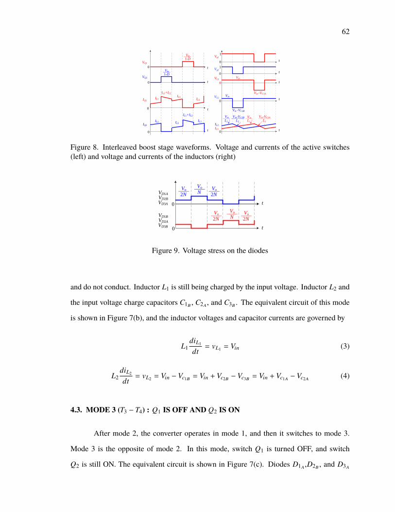
62
t
t
t
t
VQ1
IQ1
VQ2
IQ2
0
0
0
0
IL2
IL1
IL1+IL2
IL1+IL2
IL2IL2
IL1IL1
1-DVin____
1-DVin____
t
t
t
t
t
Vg1
Vg2
IL1
VL1
VL2
IL2
Vin
Vin -VC1B
0
0
0
0
0
Vin -VC1AVin
1
1
L2
Vin-VC1B_______ _______L1
Vin-VC1A
L2
Vin____L1
Vin____
Figure 8. Interleaved boost stage waveforms. Voltage and currents of the active switches(left) and voltage and currents of the inductors (right)
t
VD3A t
N
Vo____
2N
Vo____
N
Vo____
2N
Vo____
VD1A
VD2B
VD3B
VD1B
VD2A
0
0
2N
Vo____
2N
Vo____
Figure 9. Voltage stress on the diodes
and do not conduct. Inductor L1 is still being charged by the input voltage. Inductor L2 and
the input voltage charge capacitors C1B , C2A, and C3B . The equivalent circuit of this mode
is shown in Figure 7(b), and the inductor voltages and capacitor currents are governed by
L1diL1
dt= vL1 = Vin (3)
L2diL2
dt= vL2 = Vin − Vc1B = Vin + Vc2B − Vc3B = Vin + Vc1A − Vc2A (4)
4.3. MODE 3 (T3 − T4) : Q1 IS OFF AND Q2 IS ON
After mode 2, the converter operates in mode 1, and then it switches to mode 3.
Mode 3 is the opposite of mode 2. In this mode, switch Q1 is turned OFF, and switch
Q2 is still ON. The equivalent circuit is shown in Figure 7(c). Diodes D1A,D2B , and D3A

63
are forward-biased. Diodes D1B , D2A, and D3B are reverse-biased, and they are OFF. The
inductor L1 transfers its energy to the VMC stage, while L2 starts drawing power from the
source. The state equations are given by
L1diL1
dt= vL1 = Vin − Vc1A = Vin + Vc2A − Vc3A = Vin + Vc1B − Vc2B (5)
To find the voltage transfer function, one can apply the voltage second balance to the inductor
voltages. So, the average value of the voltage across the inductors L1 and L2 are given by
〈vL1〉 =
∫ dT
0Vindt +
∫ T
dT(Vin − VC1A
)dt = 0 (6)
〈vL2〉 =
∫ dT
0Vindt +
∫ T
dT(Vin − VC1B
)dt = 0 (7)
From previous equations, the capacitor voltage can be obtained. The first-stage
capacitor voltage is given by
VC1A= VC1B
=Vin
1 − d(8)
The relationship between the second-stage capacitor voltage and the first-stage capacitor
voltage can be given by
VC2A = VC2B = Vc1A + Vc1B =2Vin
1 − d(9)
The third-stage capacitor voltage is given by
Vc3A = Vc3B = Vc2A + Vc2B − Vc1B =3Vin
1 − d(10)
64
The output voltage is the sum of the voltages across the last-stage capacitors. Therefore,
the voltage gain ratio for the proposed converter with a three-stage VMC is given by
Vo
Vin=
61 − d
(11)
One can generalize the equations for the N th stage converter. The capacitor voltages in each
stage are given by
VcNA = VcNB =NVin
1 − d(12)
The output voltage for the N th stage converter is given by
Vo = VcNA + VcNB =2NVin
1 − d(13)
Therefore, the voltage gain ratio is given by
Vo
Vin=
2N1 − d
(14)
Equation 14 is an ideal gain at d1 = d2 and a single input Vin. However, the converter can
work with asymmetrical duty cycle ratios and also with two independent power sources.
Table 1 summarizes the output voltage gain at different duties as well as with two different
independent input voltage sources.
Table 1. Output voltage at different cases
Case the output voltage
d1 , d2 and Vin1 , Vin2 N(Vin11−d1+
Vin21−d2)
d1 , d2 and Vin1 = Vin2 NVin(1
1−d1+ 1
1−d2)
d1 = d2 and Vin1 , Vin2N
1−d (Vin1 + Vin2)
d1 = d2 and Vin1 = Vin22NVin1−d

65
Duty
0.5 0.55 0.6 0.65 0.7 0.75 0.8 0.85 0.9
Gain
10
20
30
40
50
60
70
80
90
100N=1N=2
N=3
N=4N=5
Figure 10. Voltage gain vs. the duty cycle at different numbers of VMC stages.
Increasing the number of VMC stages increases the voltage-gain ratio, as shown
in Figure 10. However, practical voltage gain might be reduced due to the nonidealities.
The proposed converter can be compared to various interleaved topologies, such as the
interleaved boost converter with a Dickson voltage multiplier that was proposed in [26].
The circuit in [26] suffers from high voltage stress on its capacitors as the number of stages
increases, and that might be challenging in high power applications. The modified Dickson
voltage multiplier that was proposed in [25] is an improved version of the converter in [26].
The circuit connects the output ground to the first stage of the Dickson VMC, and therefore
some of the internal capacitors have reduced voltage stress. However, the output capacitor
still has high voltage stress. Another drawback of the aforementioned converters is that
there is an uneven current share between the inductors when the converter has an even
number of VMC stages. Table 2 shows a comparison summary of the proposed converter
with the converters presented in [26] and [25]. The proposed converter has the lowest
maximum stress and the highest voltage-gain ratio. The active switch voltage stress is also
the lowest. The voltage stress across diodes is equal to the converter proposed in [25].
Both the converter presented in [25] and the proposed converter have a floating output
feature, which requires a differential voltage sensor for voltage feedback. Nevertheless, the
grounded output load is not necessary to interface the PV panels, where the control circuit
goal is to extract the maximum power.
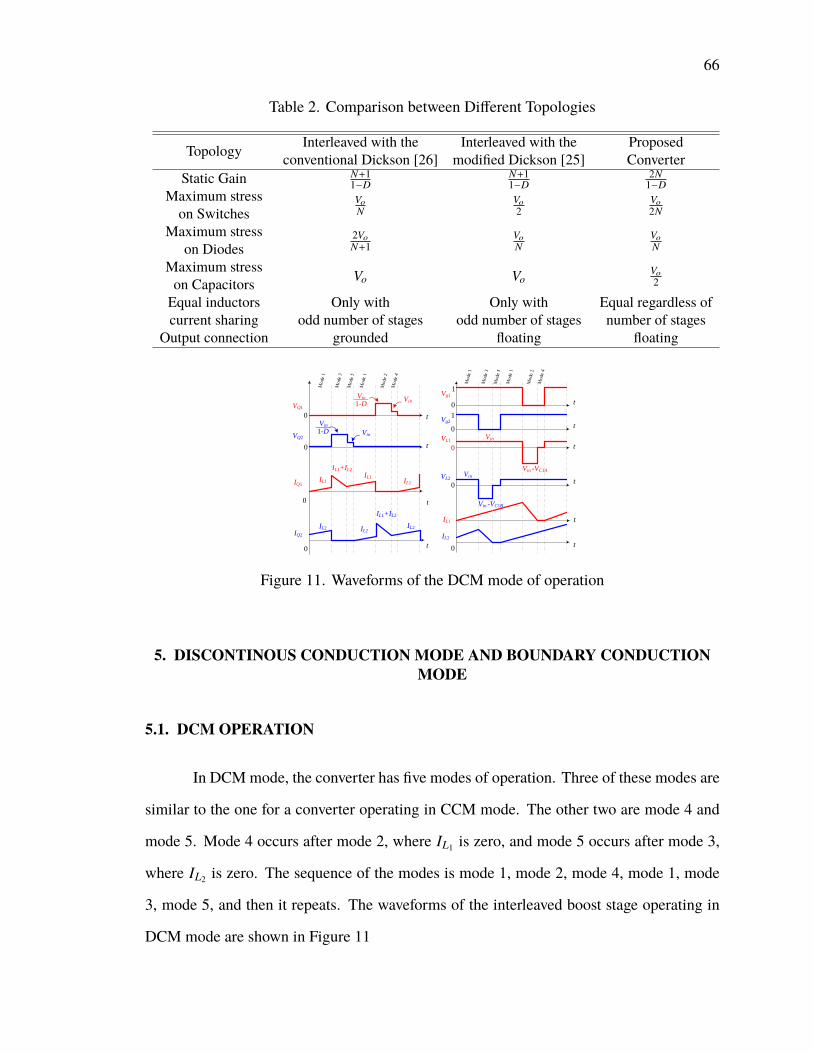
66
Table 2. Comparison between Different Topologies
Topology Interleaved with theconventional Dickson [26]
Interleaved with themodified Dickson [25]
ProposedConverter
Static Gain N+11−D
N+11−D
2N1−D
Maximum stresson Switches
Vo
NVo
2Vo
2N
Maximum stresson Diodes
2Vo
N+1Vo
NVo
N
Maximum stresson Capacitors Vo Vo
Vo
2
Equal inductorscurrent sharing
Only withodd number of stages
Only withodd number of stages
Equal regardless ofnumber of stages
Output connection grounded floating floating
t
t
t
t
VQ1
IQ1
VQ2
IQ2
0
0
0
0
IL2
IL1
IL1+IL2
IL1+IL2
IL2IL2
IL1IL1
1-DVin____
1-DVin____
t
t
t
t
t
Vg1
Vg2
IL1
VL1
VL2
IL2
Vin
Vin -VC1B
0
0
0
0
0
Vin -VC1AVin
1
1
t
Vin
Vin
Figure 11. Waveforms of the DCM mode of operation
5. DISCONTINOUS CONDUCTION MODE AND BOUNDARY CONDUCTIONMODE
5.1. DCM OPERATION
In DCMmode, the converter has five modes of operation. Three of these modes are
similar to the one for a converter operating in CCM mode. The other two are mode 4 and
mode 5. Mode 4 occurs after mode 2, where IL1 is zero, and mode 5 occurs after mode 3,
where IL2 is zero. The sequence of the modes is mode 1, mode 2, mode 4, mode 1, mode
3, mode 5, and then it repeats. The waveforms of the interleaved boost stage operating in
DCM mode are shown in Figure 11
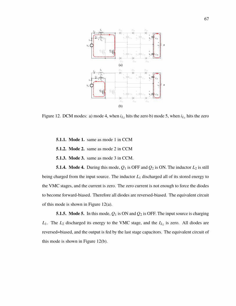
67
(a)
(b)
C3A
+
v _
R
C3A
C3B
+
v _
C3B
C2A
+
v _
C2A
C2B
+
v _
C2B
C1A
+
v _
C1A
C1B
+
v _
C1B
D1A D2A D3A
D1B D2B D3B
+
vo _
Vin
L1
Q1Q2
L2
iin
iL1
iL2
L1 + v _
+ v _L2
C3A
+
v _
R
C3A
C3B
+
v _
C3B
C2A
+
v _
C2A
C2B
+
v _
C2B
C1A
+
v _
C1A
C1B
+
v _
C1B
D1A D2A D3A
D1B D2B D3B
+
vo _
Vin
L1
Q1Q2
L2
iin
iL1
iL2
L1 + v
_
+ v _L2
Figure 12. DCMmodes: a) mode 4, when iL2 hits the zero b) mode 5, when iL1 hits the zero
5.1.1. Mode 1. same as mode 1 in CCM
5.1.2. Mode 2. same as mode 2 in CCM
5.1.3. Mode 3. same as mode 3 in CCM.
5.1.4. Mode 4. During this mode, Q1 is OFF and Q2 is ON. The inductor L2 is still
being charged from the input source. The inductor L1 discharged all of its stored energy to
the VMC stages, and the current is zero. The zero current is not enough to force the diodes
to become forward-biased. Therefore all diodes are reversed-biased. The equivalent circuit
of this mode is shown in Figure 12(a).
5.1.5. Mode 5. In this mode, Q1 is ON and Q2 is OFF. The input source is charging
L1. The L2 discharged its energy to the VMC stage, and the IL2 is zero. All diodes are
reversed=biased, and the output is fed by the last stage capacitors. The equivalent circuit of
this mode is shown in Figure 12(b).
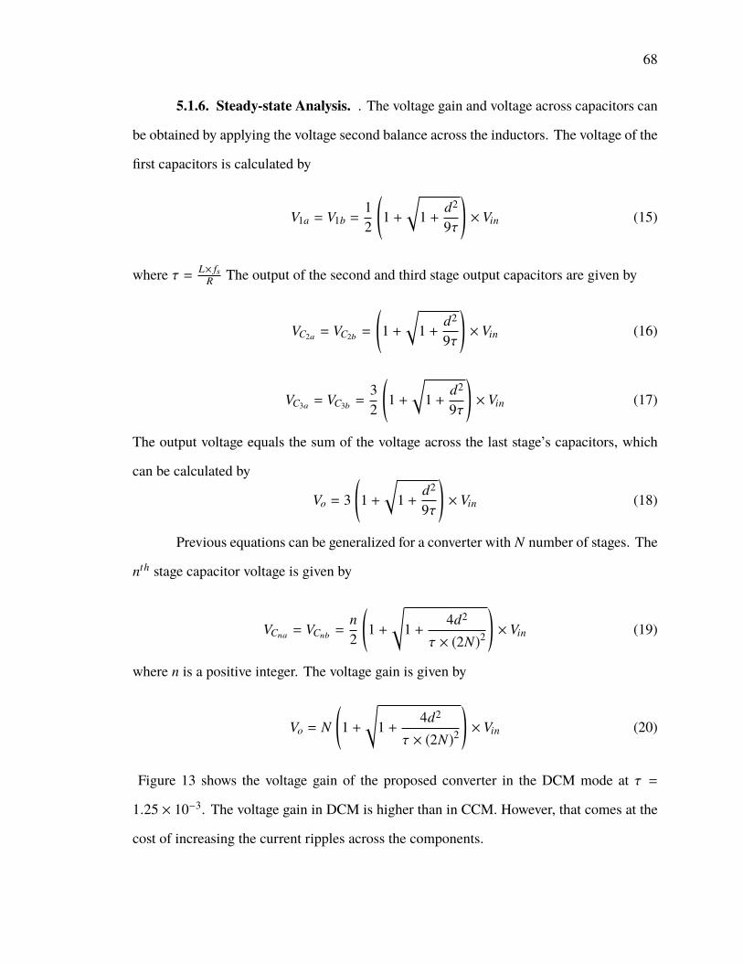
68
5.1.6. Steady-state Analysis. . The voltage gain and voltage across capacitors can
be obtained by applying the voltage second balance across the inductors. The voltage of the
first capacitors is calculated by
V1a = V1b =12
(1 +
√1 +
d2
9τ
)× Vin (15)
where τ = L× fsR The output of the second and third stage output capacitors are given by
VC2a = VC2b =
(1 +
√1 +
d2
9τ
)× Vin (16)
VC3a = VC3b =32
(1 +
√1 +
d2
9τ
)× Vin (17)
The output voltage equals the sum of the voltage across the last stage’s capacitors, which
can be calculated by
Vo = 3
(1 +
√1 +
d2
9τ
)× Vin (18)
Previous equations can be generalized for a converter with N number of stages. The
nth stage capacitor voltage is given by
VCna = VCnb=
n2
(1 +
√1 +
4d2
τ × (2N)2
)× Vin (19)
where n is a positive integer. The voltage gain is given by
Vo = N
(1 +
√1 +
4d2
τ × (2N)2
)× Vin (20)
Figure 13 shows the voltage gain of the proposed converter in the DCM mode at τ =
1.25 × 10⁻³. The voltage gain in DCM is higher than in CCM. However, that comes at the
cost of increasing the current ripples across the components.
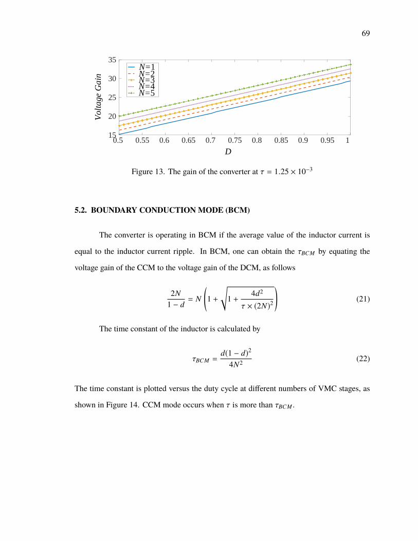
69
0.5 0.55 0.6 0.65 0.7 0.75 0.8 0.85 0.9 0.95 115
20
25
30
35N=1N=2N=3N=4N=5
D
Volt
age
Ga
in
Figure 13. The gain of the converter at τ = 1.25 × 10⁻³
5.2. BOUNDARY CONDUCTION MODE (BCM)
The converter is operating in BCM if the average value of the inductor current is
equal to the inductor current ripple. In BCM, one can obtain the τBCM by equating the
voltage gain of the CCM to the voltage gain of the DCM, as follows
2N1 − d
= N
(1 +
√1 +
4d2
τ × (2N)2
)(21)
The time constant of the inductor is calculated by
τBCM =d(1 − d)2
4N2 (22)
The time constant is plotted versus the duty cycle at different numbers of VMC stages, as
shown in Figure 14. CCM mode occurs when τ is more than τBCM .
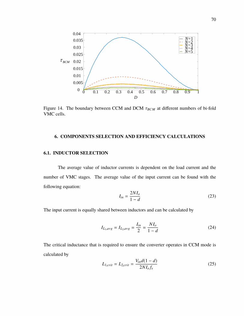
70
0 0.1 0.2 0.3 0.4 0.5 0.6 0.7 0.8 0.9 10
0.005
0.01
0.015
0.02
0.025
0.03
0.035
0.04N=1N=2N=3N=4N=5
D
BCM
Figure 14. The boundary between CCM and DCM τBCM at different numbers of bi-foldVMC cells.
6. COMPONENTS SELECTION AND EFFICIENCY CALCULATIONS
6.1. INDUCTOR SELECTION
The average value of inductor currents is dependent on the load current and the
number of VMC stages. The average value of the input current can be found with the
following equation:
Iin =2NIo
1 − d(23)
The input current is equally shared between inductors and can be calculated by
IL1,avg = IL2,avg =Iin
2=
NIo
1 − d(24)
The critical inductance that is required to ensure the converter operates in CCM mode is
calculated by
L1,crit = L2,crit =Vind(1 − d)
2NIo fs(25)

71
Inductors are normally designed based on the desired value of the inductor current ripple.
The equations for L1 and L2 selection are
L1 =Vind∆iL1 fs
(26)
L2 =Vind∆iL2 fs
(27)
The peak value of the inductor current is obtained by
IL1,pk =NIo
1 − d+
Vind2L1 fs
(28)
IL2,pk =NIo
1 − d+
Vind2L2 fs
(29)
The RMS current of the inductors is given by
IL1,RMS =
√( NIo
1 − d
)2+
( Vind
2√
3L1 fs
)2(30)
IL2,RMS =
√( NIo
1 − d
)2+
( Vind
2√
3L2 fs
)2(31)
6.2. ACTIVE SWITCH SELECTION
The active switches are implemented using MOSFETs due to their ability to operate
at high switching frequencies. To select MOSFETs for this topology, the maximum stresses
on the switches need to be calculated. The voltage stress on the MOSFETs depends on the
number of stages. The stresses on the active switches are given by
VQ1 = VQ2 =Vo
2N=
Vin
1 − d(32)

72
The maximum current that passes through the switches is given by
IS,pk =2NIo
1 − D+
Vind2L fs
(33)
The average currents passing through the active switches are given by
IQ1,pk = IQ2,pk =2NIo
1 − d+
Vind2L fs
(34)
IQ1,avg = IQ2,avg =NIo
1 − d(35)
The RMS value is approximated by the following equation:
IQ1,rms = IQ2,rms =NIod√(1 − d)3
(36)
6.3. DIODE SELECTION
One of the advantages of this topology is that the voltage stresses across the diode
also depend on the number of stages. The more stages, the less voltage stress on the diodes.
The maximum voltage that the diodes have to block is calculated by
VDNmax=
Vo
N(37)
The total average currents of the diode are given by
IDNA= IDNB
=Vo
R(38)
The RMS current is given by
IDNA,rms = IDNB
,rms =Vo
R
√1
1 − d(39)
73
6.4. CAPACITORS SELECTION
The capacitors selection is determined by the maximum current and voltage rating.
The maximum voltage stress across the capacitors is already calculated in. Equally impor-
tant, the maximum allowed voltage ripple and frequency determine the minimum required
capacitance. Both capacitors in each VMC stage have to be equal to ensure equal current
sharing operation [33]. The output capacitor selection depends on the allowed voltage rip-
ples. Both output capacitors have to be equal, and they are selected based on the following
equation:
C =Io(1 − D)Ts
∆VC1
(40)
The RMS current of the capacitors can be given by
IC3A,rms = IC3B,rms = Io
√d
1 − d(41)
IC1A,rms = IC1B,rms = Io
(1 +
√d
1 − d
)(42)
IC2A,rms = IC2B,rms = Io
(1 +
√d
1 − d
)(43)
6.5. EFFICIENCY ANALYSIS
The conduction loss in the DC resistance of the inductor (RL) is given by
PL =
φ∑i=1
I2Li,rms
× RLi (44)
74
In cases of φ = 2, L1 = L2, and RL1 = RL2 , the conduction power loss in the inductors can
be given by
PLtot = 2RL[N2
(1 − d)2V2
o
R2 +d2V2
in
(2√
3L fs)2] (45)
The total switching loss in both MOSFETs is calculated by
PQ1SW= PQ2SW
=f Vin
2(1 − d)2(NIo(Ton + To f f ) + CossVin) (46)
where Coss is the output capacitance of the MOSFETs, and Ton and To f f are the turn on and
turn off times [34]. The conduction loss in the MOSFET is given by
PQ1con + PQ2con = IQ1,rms RON1 + IQ2,rms RON2 (47)
The conduction power loss of the diode can be calculated by
PD =
N∑i=1
IDavg × VF +
N∑i=1
IDrms × r f (48)
The power loss through a capacitor is given by
PC = I2Crms
ESR (49)
The total power loss is given by
PLoss = PLtot +
φ∑i=1
PQi,SW +
φ∑i=1
PQi,cond
+
2N∑n=1
PDn +
2N∑n=1
PCn (50)
75
The efficiency of the converter is given by
η (%) = 1
1+PLtot
+∑φi=1 PQi,SW
+∑φi=1 PQi,cond
+∑2Nn=1 PDn+
∑2Nn=1 PCn
Vin×Iin
× 100 (51)
More detailed information about the efficiency of the proposed converter is presented in
Section 7.
7. SIMULATION
The proposed converter was simulated using the PLECS block set in the MAT-
LAB/SIMULINK software, with the variable-step continuous solver (ode23), a maximum
time step of 10−7 s, and a tolerance of 10−5. The component parameters used in this sim-
ulation are listed in Table 2. To avoid singular loops and errors, small parasitic elements
are included in the simulation. The voltage and current waveforms of the switches and
the inductors are shown in Figure 15. The maximum stress on active switches Q1 and
Q2 is 66.6 V , and the average and peak values of the switch currents are 5 A and 6.3 A,
respectively. Similarly, the average current of each inductor is 5 A, and the RMS current
is ' 5.1 A. The inductor currents are interleaved, and that can increase the frequency of
the input current ripple currents so that these ripples can be easily filtered out with smaller
capacitors than the CBC. Figure 16 shows the diodes’ voltage and current waveforms. The
maximum voltage stress on the diodes is 133.3 V , the average current is 0.5 A, and the
RMS current is 0.91 A. Figure 17 shows the waveforms of the voltage and the current of
the capacitors. The voltage across each of the output capacitors is ' 200 V , and the RMS
current is 1.26 A. The second stage capacitors have 133 V , and the RMS current is 0.76 A.
The first-stage capacitors have 57 V , and the RMS current is 0.76 A. The figure also shows
the capacitors’ voltage ripple cancellation at each stage.
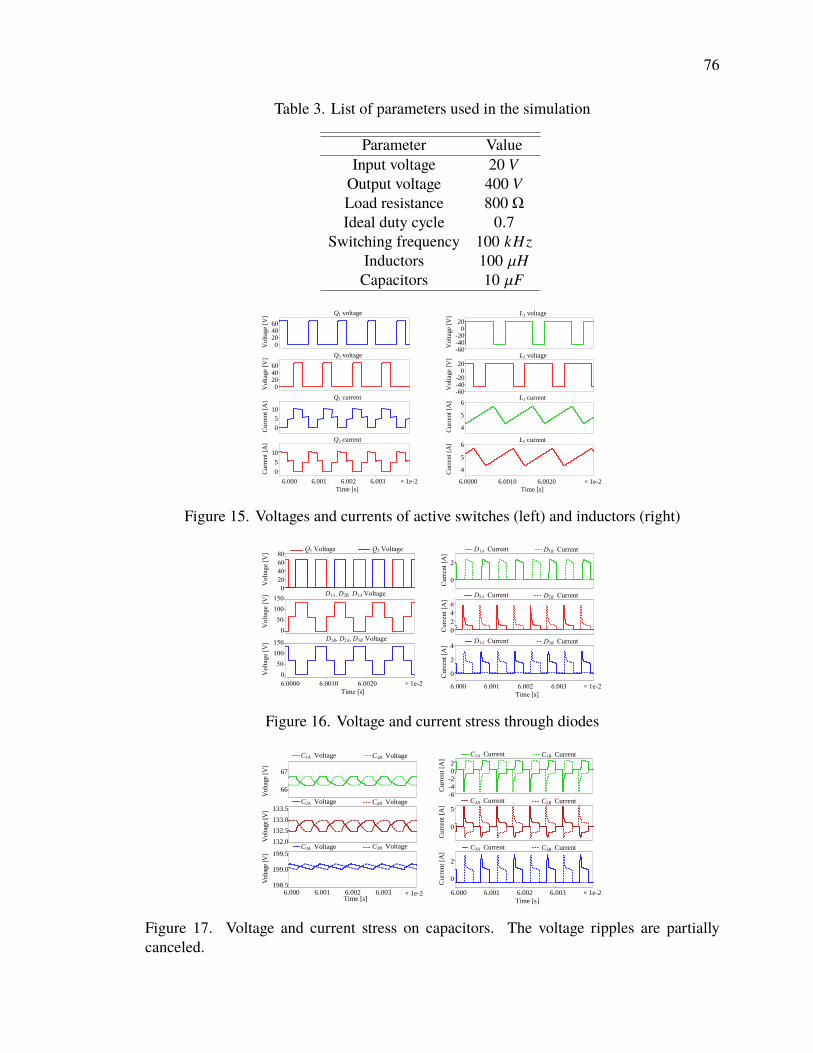
76
Table 3. List of parameters used in the simulation
Parameter ValueInput voltage 20 VOutput voltage 400 VLoad resistance 800 ΩIdeal duty cycle 0.7
Switching frequency 100 kHzInductors 100 µHCapacitors 10 µF
Q1 voltage
Q2 voltage
Q1 current
Q2 current
Volt
age
[V
]
0204060
Volt
age
[V
]
0204060
Curr
ent
[A]
0
5
10
× 1e-2
Time [s]
6.000 6.001 6.002 6.003
Curr
ent
[A]
0
5
10
L1 voltage
L2 voltage
L1 current
L2 current
Volt
age
[V
]
-60-40-20
020
Volt
age
[V
]
-60-40-20
020
Curr
ent
[A]
4
5
6
× 1e-2
Time [s]
6.0000 6.0010 6.0020
Curr
ent
[A]
4
5
6
Figure 15. Voltages and currents of active switches (left) and inductors (right)
Q1 Voltage Q2 Voltage
D1A , D2B, D3A Voltage
D1B, D2A, D3B Voltage
Volt
age
[V
]
0
20
40
60
80
Volt
age
[V
]
150
100
50
0
Volt
age
[V
] 150
100
50
0
× 1e-2
Time [s]
6.0000 6.0010 6.0020
D1A Current
D2A Current
D3A Current
Curr
ent
[A]
0
2
Curr
ent
[A]
0
2
4
6
Curr
ent
[A]
0
2
4
× 1e-2
Time [s]
6.000 6.001 6.002 6.003
D1B Current
D2B Current
D3B Current
Figure 16. Voltage and current stress through diodes
Volt
age
[V]
66
67
Volt
age
[V]
132.0
132.5
133.0
133.5
× 1e-2Time [s]
6.000 6.001 6.002 6.003
Vol
tage
[V]
198.5
199.0
199.5
C1A Current
C2A Current
C3A Current
Curr
ent
[A]
-6-4-202
Curr
ent
[A]
0
5
Curr
ent
[A]
0
2
× 1e-2
Time [s]
6.000 6.001 6.002 6.003
C1B Current
C2B Current
C3B Current
C1A Voltage
C2A Voltage
C3A Voltage
C1B Voltage
C2B Voltage
C3B Voltage
Figure 17. Voltage and current stress on capacitors. The voltage ripples are partiallycanceled.

77
Table 4. Component Listing for the Hardware Prototype
Item Designation Rating Part No.Inductor L1, L2 100 µH, DCR = 25 mΩ, 60B104C
CapacitorC1A,C2AC1BC2BC3A,C3B
10 µF EXH2E106HRPT
MOSFET Q1,Q2150 V,37 A
Rds(on) = 10.525 mΩ IPA105N15N3
Diode D1A,D2AD1B,D2B
250V,40AVF = 0.86 V, trr = 35 ns MBR40250G
load Rload multiple values L100J100E, L225J50REL225J250E,L225J500E
8. EXPERIMENTAL IMPLEMENTATION AND RESULTS
A 200 W hardware prototype was implemented experimentally to verify the analysis
and simulation presented in the previous sections. Figure 18 shows the annotated prototype
board of the proposed converter. The converter was designed for a nominal converter
ratio 40020 = 20 and a duty cycle of 0.7. The switching frequency was 50 kHz. The
components used to implement the prototype are listed in Table 4. The active switches
were implemented using MOSFETs IPA105N15N3 for their low on-resistance, low gate
capacitance, and low switching power loss. Schottky diodes MBR40250G were selected
to implement the blocking diodes of the VMC because of their fast recovery time as well
as their relatively low forward voltage. Film capacitors were selected to implement the
blocking and output capacitors, which have a low equivalent series resistance and a high
voltage rating. The converter was fed by the N5766A DC power supply to power a 200 W
load, which was implemented using a combination of ceramic resistors. Figure 18 shows the
thermal image of the converter operating at 100 W , and it shows that the active switches are
the only part that is heating up. Figure 19 shows the inductors and active switch currents at
80 W . Each inductor current has an average value of 2 A and a peak current of' 2.1 A. They
are shifted 180, and that doubles the input current ripple frequency as shown. Figure 20
shows the voltage stress across Q1 and Q2, as well as the diodes; the stresses across the
active switches are 66 V , and the maximum voltage on the diodes is 133 V .
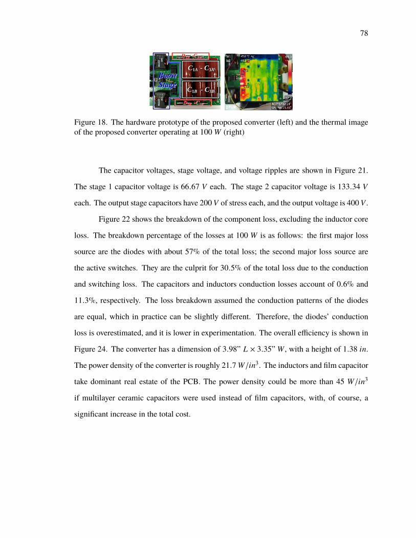
78
C1B - C3B
C1A - C3A
D1A -C3A
D1B -C3B
Figure 18. The hardware prototype of the proposed converter (left) and the thermal imageof the proposed converter operating at 100 W (right)
The capacitor voltages, stage voltage, and voltage ripples are shown in Figure 21.
The stage 1 capacitor voltage is 66.67 V each. The stage 2 capacitor voltage is 133.34 V
each. The output stage capacitors have 200 V of stress each, and the output voltage is 400 V .
Figure 22 shows the breakdown of the component loss, excluding the inductor core
loss. The breakdown percentage of the losses at 100 W is as follows: the first major loss
source are the diodes with about 57% of the total loss; the second major loss source are
the active switches. They are the culprit for 30.5% of the total loss due to the conduction
and switching loss. The capacitors and inductors conduction losses account of 0.6% and
11.3%, respectively. The loss breakdown assumed the conduction patterns of the diodes
are equal, which in practice can be slightly different. Therefore, the diodes’ conduction
loss is overestimated, and it is lower in experimentation. The overall efficiency is shown in
Figure 24. The converter has a dimension of 3.98” L × 3.35” W , with a height of 1.38 in.
The power density of the converter is roughly 21.7 W/in3. The inductors and film capacitor
take dominant real estate of the PCB. The power density could be more than 45 W/in3
if multilayer ceramic capacitors were used instead of film capacitors, with, of course, a
significant increase in the total cost.

79
IL1=2A (2A/Div) IL2=2A (2A/Div)
Iin= 4 A (2A/Div)
IQ1 (5 A/Div)
IQ2 (5A/Div)
Figure 19. Inductor currents and smooth pre-filtered input current (left) and active switchescurrents (right)
VQ2 = 66 V (100 V/div)
VQ1 = 66 V (100 V/div)
Gate signal 1 10 V (20 V/div)
Gate signal 2 10 V (20 V/div)
T = 20 µs Gate signal 1 10 V (20 V/div)
VD1A = 133.3 V (100 V/div)
VD2A = 133.3 V (100 V/div)
VD3A = 133.3 V (100 V/div)
Gate signal 1 10 V (20 V/div)
VD1B = 66.6 V (100 V/div)
VD2B = 133.3 V (100 V/div)
VD3B = 133.3 V (100 V/div)
Figure 20. Voltage stress across active switches and diodes

80
ΔVC3A (0.5 V/div) ΔVC3B (0.5 V/div)
Δ(VC3A + VC3B ) (2.5 V/div)
Gate signal 1 10 V (20 V/div)
ΔVC2A (1 V/div) ΔVC2B = (1 V/div)
Δ(VC2A + VC2B ) = (2.5 V/div)
Gate signal 1 10 V (20 V/div)
ΔVC1A (1 V/div) ΔVC1B = (1 V/div)
Δ(VC1A + VC1B ) = (2.5 V/div)
Gate signal 1 10 V (20 V/div)Gate signal 1 10 V (20 V/div)
VC1A+VC1B = 133.3 V (250 V/div)
VC2A+VC2B = 266.66 V (100 V/div)
Vo=VC3A+VC3B = 400 V (100 V/div)
Figure 21. Capacitor voltages and AC voltage ripples
0 50 100 150 200 250 300 350 4000
10
20
30
40
50
60
70
80
90
100
MOSFETs conduction loss MOSFETs switching loss Diodes Inductors Capacitors
Load power [W]0 50 100 150 200 250 300 350 400
0
2
4
6
8
10
12
14
Loss
bre
akdow
n p
erc
enta
ge %
Com
ponen
t pow
er
loss
[W
]
57.6%
11.3%
31 .7%
16.8%
0.6%
Load power [W]
Figure 22. Loss (left) and loss distribution (right) of the converter as a function of the load.
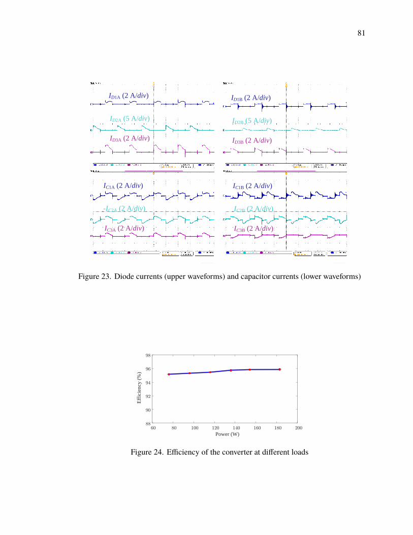
81
ID2B (5 A/div)
ID1B (2 A/div)
ID3B (2 A/div)
ID2A (5 A/div)
ID1A (2 A/div)
ID3A (2 A/div)
-IC2A (2 A/div)
IC1A (2 A/div)
IC3A (2 A/div)
IC2B (2 A/div)
IC1B (2 A/div)
IC3B (2 A/div)
Figure 23. Diode currents (upper waveforms) and capacitor currents (lower waveforms)
Power (W)
60 80 100 120 140 160 180 200
Eff
icie
ncy
(%)
88
90
92
94
96
98
Figure 24. Efficiency of the converter at different loads

82
9. CONCLUSION
This paper has presented a high-voltage-gain DC-DC step-up converter to interface
renewable energy sources to a higher voltage DC bus, such as a 20 V input source to a
400 VDC . The converter employs a bi-fold Dickson VMC with an interleaved boost stage to
obtain a high voltage gain. Several featuresmake the converter desirable, such as low voltage
stress across components, modularity, and the continuity of the input current. The converter
balances the capacitor voltages and features equal current sharing among phases, which
improves the conduction losses on both inductors andMOSFETs. Additionally, the proposed
converter is capable of converting power from either a single or two independent PV panels.
An analysis of the converter and the selection of the components are discussed in detail
and supported by the simulation results. A 200-W hardware prototype was implemented to
validate the analysis and the simulation.
REFERENCES
[1] “New hikari supercomputer starts solar hvdc,” https://www.tacc.utexas.edu/-/new-hikari-supercomputer-starts-solar-hvdc, (Accessed on 02/12/2018).
[2] M. E. Baran and N. R. Mahajan, “Dc distribution for industrial systems: opportunitiesand challenges,” IEEE Transactions on Industry Applications, vol. 39, no. 6, pp.1596–1601, Nov 2003.
[3] J. G. Ciezki and R. W. Ashton, “Selection and stability issues associated with anavy shipboard dc zonal electric distribution system,” IEEE Transactions on PowerDelivery, vol. 15, no. 2, pp. 665–669, Apr 2000.
[4] A. Stupar, T. Friedli, J. Minibock, and J. W. Kolar, “Towards a 99% efficient three-phase buck-type pfc rectifier for 400-v dc distribution systems,” IEEE Transactions onPower Electronics, vol. 27, no. 4, pp. 1732–1744, April 2012.
[5] Y. Sato, Y. Tanaka, A. Fukui, M. Yamasaki, and H. Ohashi, “Sic-sit circuit break-ers with controllable interruption voltage for 400-v dc distribution systems,” IEEETransactions on Power Electronics, vol. 29, no. 5, pp. 2597–2605, May 2014.
[6] P. T. Krein, “Data center challenges and their power electronics,” CPSS Transactionson Power Electronics and Applications, vol. 2, no. 1, pp. 39–46, 2017.
83
[7] M. Kasper, D. Bortis, T. Friedli, and J. W. Kolar, “Classification and comparativeevaluation of pv panel integrated dc-dc converter concepts,” in Power Electronics andMotion Control Conference (EPE/PEMC), 2012 15th International, Sept 2012, pp.LS1e.4–1–LS1e.4–8.
[8] F. L. Tofoli, D. d. C. Pereira, W. J. de Paula, and D. d. S. Oliveira Júnior, “Survey onnon-isolated high-voltage step-up dc-dc topologies based on the boost converter,” IETPower Electronics, vol. 8, no. 10, pp. 2044–2057, 2015.
[9] B. C. Barry, J. G. Hayes, and M. S. Ryłko, “Ccm and dcm operation of the interleavedtwo-phase boost converter with discrete and coupled inductors,” IEEE Transactionson Power Electronics, vol. 30, no. 12, pp. 6551–6567, Dec 2015.
[10] R. N. A. L. e Silva Aquino, F. L. Tofoli, P. P. Praca, D. d. S. Oliveira, and L. H.S. C. Barreto, “Soft switching high-voltage gain dc-dc interleaved boost converter,”IET Power Electronics, vol. 8, no. 1, pp. 120–129, 2015.
[11] L. Huber and M. M. Jovanovic, “A design approach for server power supplies fornetworking applications,” in APEC 2000. Fifteenth Annual IEEE Applied Power Elec-tronics Conference and Exposition (Cat. No.00CH37058), vol. 2, 2000, pp. 1163–1169vol.2.
[12] Y. Gu, D. Zhang, X. Wu, and X. Zhang, “Research on stability improvement ofthe cascaded dc-dc converters based on ac signal sampling control method,” IEEETransactions on Power Electronics, vol. 33, no. 5, pp. 4547–4559, May 2018.
[13] M. T. Zhang, Y. Jiang, F. C. Lee, and M. M. Jovanovic, “Single-phase three-levelboost power factor correction converter,” in Applied Power Electronics Conferenceand Exposition, 1995. APEC ’95. Conference Proceedings 1995., Tenth Annual, no. 0,Mar 1995, pp. 434–439 vol.1.
[14] H. C. Chen and W. J. Lin, “Mppt and voltage balancing control with sensing onlyinductor current for photovoltaic-fed, three-level, boost-type converters,” IEEE Trans-actions on Power Electronics, vol. 29, no. 1, pp. 29–35, Jan 2014.
[15] Y. Zhang, J. T. Sun, and Y. F. Wang, “Hybrid boost three-level dc-dc converter withhigh voltage gain for photovoltaic generation systems,” IEEE Transactions on PowerElectronics, vol. 28, no. 8, pp. 3659–3664, Aug 2013.
[16] Q. M. Li and F. C. Lee, “Design consideration of the active-clamp forward converterwith current mode control during large-signal transient,” IEEE Transactions on PowerElectronics, vol. 18, no. 4, pp. 958–965, July 2003.
[17] R. Ayyanar and N. Mohan, “Novel soft-switching dc-dc converter with full zvs-rangeand reduced filter requirement. i. regulated-output applications,” IEEE Transactionson Power Electronics, vol. 16, no. 2, pp. 184–192, Mar 2001.

84
[18] K. C. Tseng and C. C. Huang, “High step-up high-efficiency interleaved converterwith voltage multiplier module for renewable energy system,” IEEE Transactions onIndustrial Electronics, vol. 61, no. 3, pp. 1311–1319, March 2014.
[19] A. Abramovitz, T. Cheng, and K. Smedley, “Analysis and design of forward converterwith energy regenerative snubber,” IEEE Transactions on Power Electronics, vol. 25,no. 3, pp. 667–676, March 2010.
[20] G. Spiazzi, P. Mattavelli, and A. Costabeber, “High step-up ratio flyback converterwith active clamp and voltage multiplier,” IEEE Transactions on Power Electronics,vol. 26, no. 11, pp. 3205–3214, Nov 2011.
[21] B. Axelrod, Y. Berkovich, and A. Ioinovici, “Switched-capacitor/switched-inductorstructures for getting transformerless hybrid dc-dc pwm converters,” IEEE Transac-tions on Circuits and Systems I: Regular Papers, vol. 55, no. 2, pp. 687–696, March2008.
[22] Y. J. A. Alcazar, D. de Souza Oliveira, F. L. Tofoli, and R. P. Torrico-Bascopé, “Dc-dc nonisolated boost converter based on the three-state switching cell and voltagemultiplier cells,” IEEE Transactions on Industrial Electronics, vol. 60, no. 10, pp.4438–4449, Oct 2013.
[23] J. C. Rosas-Caro, J. M. Ramirez, F. Z. Peng, and A. Valderrabano, “A dc-dc multilevelboost converter,” IET Power Electronics, vol. 3, no. 1, pp. 129–137, January 2010.
[24] B. Wu, S. Li, Y. Liu, and K. M. Smedley, “A new hybrid boosting converter forrenewable energy applications,” IEEE Transactions on Power Electronics, vol. 31,no. 2, pp. 1203–1215, Feb 2016.
[25] B. Baddipadiga and M. Ferdowsi, “A high-voltage-gain dc-dc converter based onmodified Dickson charge pump voltage multiplier,” IEEE Transactions on PowerElectronics, vol. PP, no. 99, pp. 1–1, 2016.
[26] V.A.K. Prabhala, P. Fajri, V. S. P. Gouribhatla, B. P. Baddipadiga, andM. Ferdowsi, “Adc-dc converter with high voltage gain and two input boost stages,” IEEE Transactionson Power Electronics, vol. 31, no. 6, pp. 4206–4215, June 2016.
[27] G. Palumbo and D. Pappalardo, “Charge pump circuits: An overview on designstrategies and topologies,” IEEE Circuits and Systems Magazine, vol. 10, no. 1, pp.31–45, First 2010.
[28] Y. Lei, R. May, and R. Pilawa-Podgurski, “Split-phase control: Achieving completesoft-charging operation of a dickson switched-capacitor converter,” IEEE Transactionson Power Electronics, vol. 31, no. 1, pp. 770–782, Jan 2016.
[29] A. Alzahrani, P. Shamsi, and M. Ferdowsi, “Analysis and design of bipolar dicksondc-dc converter,” in 2017 IEEE Power and Energy Conference at Illinois (PECI), Feb2017, pp. 1–6.
85
[30] ——, “Boost converter with bipolar dickson voltagemultiplier cells,” in 2017 IEEE 6thInternational Conference on Renewable Energy Research and Applications (ICRERA),Nov 2017, pp. 228–233.
[31] I. G. Hansen and G. R. Sundberg, “Space station 20 − khz power management anddistribution system,” in 1986 17th Annual IEEE Power Electronics Specialists Con-ference, June 1986, pp. 676–683.
[32] A. Alzahrani, P. Shamsi, and M. Ferdowsi, “A novel interleaved non-isolated high-gain dc-dc boost converter with Greinacher voltage multiplier cells,” in 2017 IEEE 6thInternational Conference on Renewable Energy Research and Applications (ICRERA),Nov 2017, pp. 222–227.
[33] C. T. Pan, C. F. Chuang, and C. C. Chu, “A novel transformer-less adaptable voltagequadrupler dc converter with low switch voltage stress,” IEEE Transactions on PowerElectronics, vol. 29, no. 9, pp. 4787–4796, Sept 2014.
[34] Y. Xiong, S. Sun, H. Jia, P. Shea, and Z. J. Shen, “New physical insights on powermosfet switching losses,” IEEE Transactions on Power Electronics, vol. 24, no. 2, pp.525–531, Feb 2009.
86
III. A FAMILY OF HIGH-VOLTAGE-GAIN MULTILEVEL BOOSTCONVERTERS
Ahmad Alzahrani, Pourya Shamsi, and Mehdi Ferdowsi
Departement of Electrical and Computer Engineering
Missouri University of Science and Technology
asakw9, shamsip, [email protected]
ABSTRACT
This paper presents various topologies based on multilevel boost converters, with
a focus on those derived from three-level boost converters (TLB). The TLB is a common
dc-dc step-up topology and is widely used in various applications, such as power factor cor-
rection (PFC) and voltage regulation. Using such topology in applications that require high
voltage gain is a challenge because of the insufficient voltage gain. The proposed family
utilizes several different techniques to increase the voltage gain of the TLB. These tech-
niques include using coupled inductors, switched inductor cells, or a flyback transformer.
An example converter of TLB with a flyback transformer is fully illustrated with modes
of operation, a steady-state analysis and component selection. The converter simulated to
proof the theory and analysis , which is used to convert a 20 V to 200 V . The converter
was also simulated to extract power from three PVL-136 photovoltaic (PV) panels using an
MPPT algorithm. An 80 W hardware prototype was implemented in the lab to validate the
simulation and the analysis.
Keywords: High-Gain, three-Level, dc-dc, boost, self-left, coupled inductor, flyback,
MPPT, solar, PV

87
1. INTRODUCTION
Power electronics converters have an indispensable role in integrating renewable
energy sources to the electric power grid. As more renewable energy sources are used, more
efficient components and converters are desirable. Renewable energy sources, in general,
suffer from low voltage output and high dependence on weather conditions. Photovoltaics
energy also has one more issue, which is shading. Shading can reduce the output power
of the solar panel and possibly even create hot spots, which might lead to damage in the
solar cell itself. The stochastic nature of the PV output leads to a variable maximum
power point and variable input voltage, which necessitates a maximum power point tracker
(MPPT) [1–3]. Connecting several panels in series increases the overall voltage and power.
However, voltage mismatches between cells leads to a reduction of efficiency and output
power. Connecting solar panels in parallel increases the total current, but the voltage is still
as that of a single cell [4–6].
In this case, a step up converter with a high-voltage-gain ratio is needed. The CBC
can achieve high gain at high duty cycles, in theory. In reality, achieving high gain with
the CBC is impracticable because of the conduction losses and the nonidealities [7, 8].
Also using the CBC to operate in the continuous conduction mode (CCM) requires bulky
magnetics and high rating switching devices [9–11]. The voltage gain can be increased by
cascading several CBCs. Each stage operates at a lower value duty ratio, and the overall
voltage gain is high. However, cascading two or more CBCs means processing the power
two times or more, which might reduce the performance of the converter and complicate the
control design [12, 13]. Similarly, stacking several CBCs can share the power and reduce
the current rating, but there is no improvement in the voltage gain. A hybrid flyback-boost
converter utilizes the flyback transformer to increase the voltage gain of the CBC [13].
The voltage gain of the converter is a function of the transformer turns ratio. However,
using a transformer would increase the weight and volume of the converter and decrease
the power density. The TLB converter was introduced to reduce the voltage stress of the

88
semiconductors, and reduce the size of the magnetic elements by increasing the effective
frequency. The drawback of the TLB converter is the low voltage gain, which is not sufficient
for renewable energy sources that have low voltage. The conventional isolated converters
such as flyback, forward and push-pull draw a discontinuous current from the input source,
which make them not suitable for use in renewable energy applications [14, 15].
Flying capacitor voltage multiplying converters can achieve high gain with low
voltage stress across the components and operate in the CCM with minimal inductance due
to the high effective frequency. The effective frequency value is a multiple of the switching
frequency, which is based on the number of stages [16–18]. However, the minimum duty
cycle and the phase shift is a function of the stages. That is, the greater the FCML level, the
higher the duty cycle that is required, and that limits the range of the operating duty cycle.
The narrow range of the duty cycle can be a disadvantage in cases with MPPT control and
load matching.
The voltage gain can be increased by using a transformer or a coupled inductor,
either an isolated or integrated one [19–21]. Therefore, the voltage gain becomes a function
of the turns ratio, and as gain requirement increased, so does the turns ratio requirement.
However, the leakage inductance causes voltage spikes on the active switches and requires
clamping circuits. Furthermore, employing magnetic elements with a higher turns ratio
increases the weight of the converter and reduces the power density, especially at a low
frequency. Recently, several papers introduce interleaved boost converters with switched-
capacitor circuits [22, 23]. The switched-capacitor circuit has a high power density, and the
interleaved part can minimize the magnetic storage requirement. However, using switched-
capacitor requires very complicated driving circuitry, and complicated control to remove
the mismatches between the capacitors.
This paper presents a family a high-voltage-gain step-up dc-dc converter based
on multilevel boost converter to integrate solar panels with low output voltage, typically
12 − 45 Vdc, to a dc distribution bus in a dc microgrid (200 − 960 Vdc). To implement a

89
converter with a high-gain conversion ratio, coupled-inductors and voltage multiplier cells
were incorporated to increase the voltage gain of the converter. The proposed converter
is better than paralleling or cascading boost converters in terms of efficiency and voltage
stress across components. The main advantage is that the effective frequency is seen by
the magnetic is higher than the switching frequency, which allow reduction in the magnetic
size.
The rest of the paper is structured as follows: Section 2 presents different variations
of converters belonging to the proposed family with an explanation of the technique used to
enhance the voltage gain. In Section 3, an example of the proposed converter is given and
analyzed. The component selections and efficiency analysis is presented in Section 4. In
Section 5 and 6, simulation and experimental results of the example converter are provided,
respectively. Finally, conclusions and future work are described in Section 7.
2. PROPOSED FAMILY OF MULTILEVEL BOOST CONVERTERWITH HIGHGAIN
2.1. INTERLEAVING
Although the interleaving techniques increase the frequency of the AC components
of the input current, the frequency of the AC components of the inductor current is still the
same as the switching frequency, which might not be a good trade-off for increasing the
number of elements. Topologies, such as flying capacitor multilevel converters (FCMC) and
multilevel converter families, tend to increase the effective frequency of the inductor voltage
using vertical interleaving. That is, the effective frequency usually equals the switching
frequency multiplied by the number of levels. Increasing the effective frequency that is
seen by the inductors reduces the critical inductances that ensure the continuous flow of
the inductor current and allow designers to select magnetic components with a smaller
volume and build high power density converters. At high power, the advantage of vertical
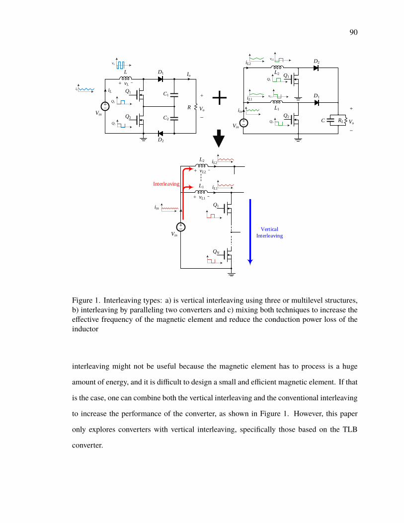
90
D1L
+
Vo
_
R
Q1
VinQ2 C2
D2
C1
+ vL _
iL
Io
L1
Q1
Vin
QN
+ vL1 _
iL1
L2
+ vL2 _
iL2
Vertical
Interleaving
Interleaving
iL
vL
Q1
Q2
L1
Q1
Q2
L2
D1
D2
RLC
Q1
Q2
vL2
vL1
iL2
iL1
iin
Vin
iin
+
Vo
_
+
Figure 1. Interleaving types: a) is vertical interleaving using three or multilevel structures,b) interleaving by paralleling two converters and c) mixing both techniques to increase theeffective frequency of the magnetic element and reduce the conduction power loss of theinductor
interleaving might not be useful because the magnetic element has to process is a huge
amount of energy, and it is difficult to design a small and efficient magnetic element. If that
is the case, one can combine both the vertical interleaving and the conventional interleaving
to increase the performance of the converter, as shown in Figure 1. However, this paper
only explores converters with vertical interleaving, specifically those based on the TLB
converter.
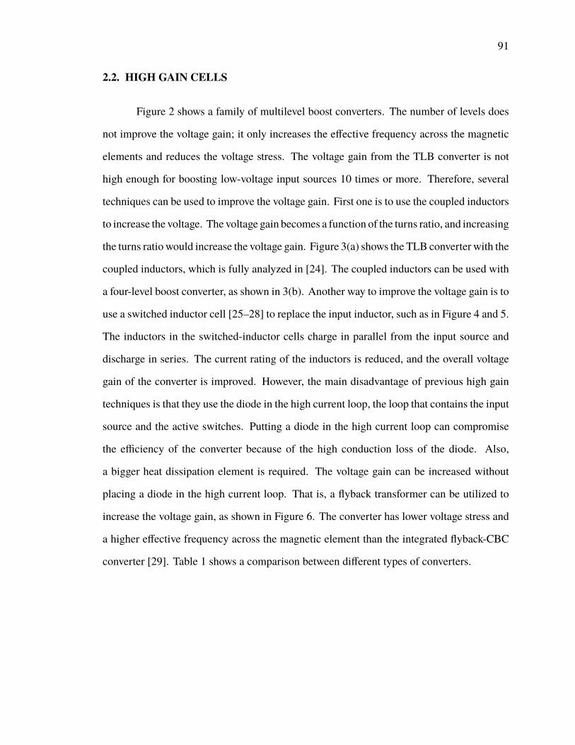
91
2.2. HIGH GAIN CELLS
Figure 2 shows a family of multilevel boost converters. The number of levels does
not improve the voltage gain; it only increases the effective frequency across the magnetic
elements and reduces the voltage stress. The voltage gain from the TLB converter is not
high enough for boosting low-voltage input sources 10 times or more. Therefore, several
techniques can be used to improve the voltage gain. First one is to use the coupled inductors
to increase the voltage. The voltage gain becomes a function of the turns ratio, and increasing
the turns ratio would increase the voltage gain. Figure 3(a) shows the TLB converter with the
coupled inductors, which is fully analyzed in [24]. The coupled inductors can be used with
a four-level boost converter, as shown in 3(b). Another way to improve the voltage gain is to
use a switched inductor cell [25–28] to replace the input inductor, such as in Figure 4 and 5.
The inductors in the switched-inductor cells charge in parallel from the input source and
discharge in series. The current rating of the inductors is reduced, and the overall voltage
gain of the converter is improved. However, the main disadvantage of previous high gain
techniques is that they use the diode in the high current loop, the loop that contains the input
source and the active switches. Putting a diode in the high current loop can compromise
the efficiency of the converter because of the high conduction loss of the diode. Also,
a bigger heat dissipation element is required. The voltage gain can be increased without
placing a diode in the high current loop. That is, a flyback transformer can be utilized to
increase the voltage gain, as shown in Figure 6. The converter has lower voltage stress and
a higher effective frequency across the magnetic element than the integrated flyback-CBC
converter [29]. Table 1 shows a comparison between different types of converters.
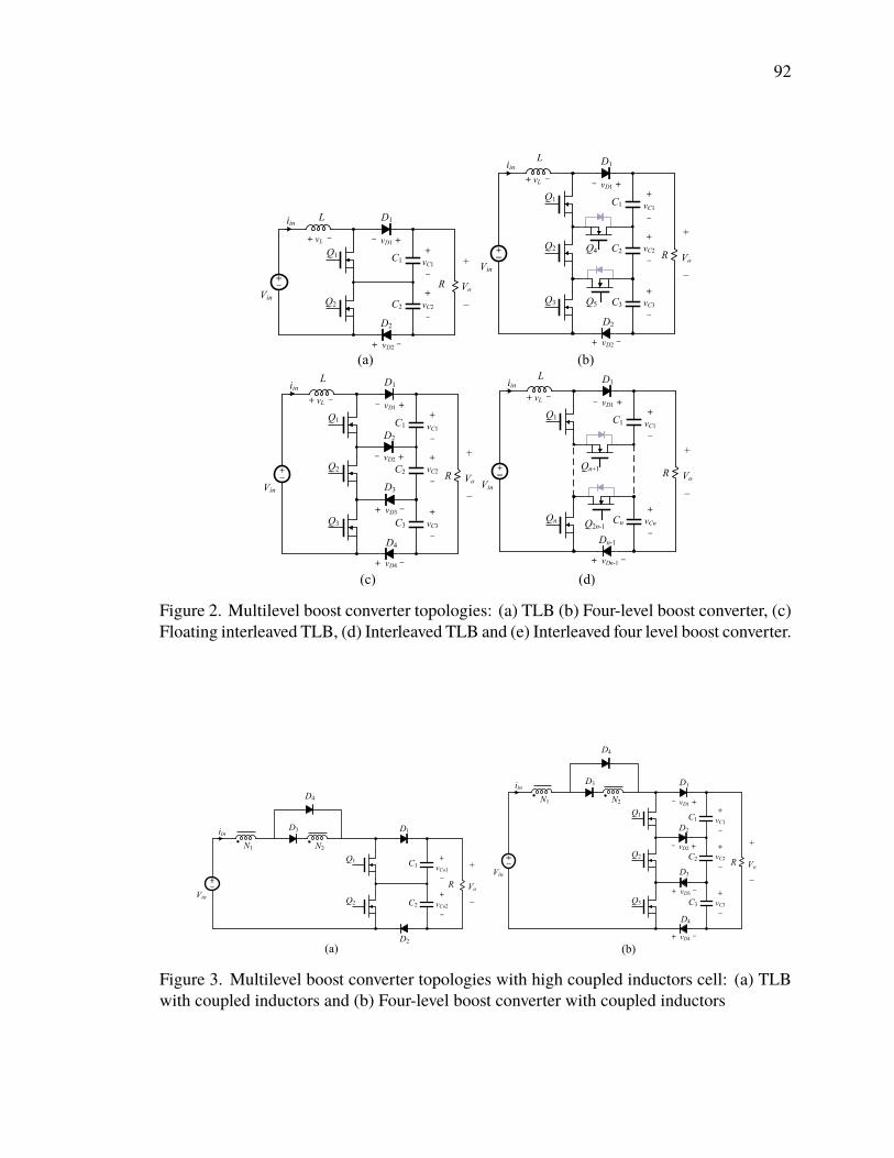
92
D1
+
Vo
_
R
Q1
VinQ2 C2
D2
C1
iin
+
vC1_
+
vC2_
_ vD1 +
+ vD2 _
+ vL _
L
D1
+
Vo
_
R
Q1
Vin
Q2 C2
D3
C1
iin
C3Q3
D2
D4
+
vC1_
+
vC2_
+
vC3_
_ vD1 +
_ vD2 +
+ vD3 _
+ vD4 _
+ vL _
L
(a) (b)
D1
+
Vo
_
R
Q1
Vin
Q2 C2
C1
iin
C3Q3
D2
+
vC1_
+
vC2_
+
vC3_
_ vD1 +
+ vD2 _
+ vL _
L
(c)
Q4
Q5
(d)
D1
+
Vo
_
R
Q1
Vin
C1
iin
CnQn
Dn-1
+
vC1_
+
vCn_
_ vD1 +
+ vDn-1 _
+ vL _
L
Qn+1
Q2n-1
Figure 2. Multilevel boost converter topologies: (a) TLB (b) Four-level boost converter, (c)Floating interleaved TLB, (d) Interleaved TLB and (e) Interleaved four level boost converter.
D1
+
Vo
_
R
Q1
VinQ2 C2
D2
C1
iin
N1 N2
D4
D3
+
vCo1_
+
vCo2_
D1
+
Vo
_
R
Q1
Vin
Q2 C2
D3
C1
C3Q3
D2
D4
+
vC1_
+
vC2_
+
vC3_
_ vD1 +
_ vD2 +
+ vD3 _
+ vD4 _
iin
N1 N2
D4
D3
(a) (b)
Figure 3. Multilevel boost converter topologies with high coupled inductors cell: (a) TLBwith coupled inductors and (b) Four-level boost converter with coupled inductors
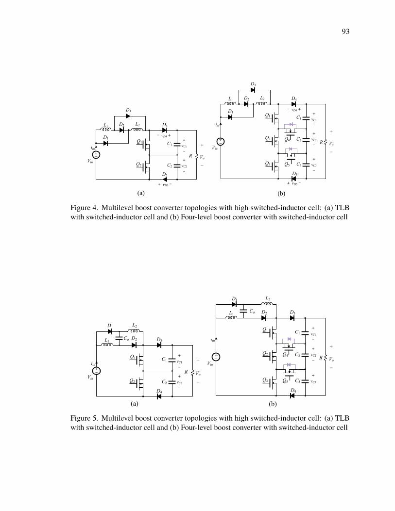
93
D4
+
Vo
_
R
Q1
VinQ2 C2
D5
C1iin
+
vC1_
+
vC2_
_ vD4 +
+ vD5 _
(a)
D4
+
Vo
_
R
Q1
Vin
Q2 C2
C1
C3Q3
D5
+
vC1_
+
vC2_
+
vC3_
_ vD4 +
+ vD5 _
(b)
Q4
Q5
D2
D1
D3
L2L1 iin
D2
D1
D3
L2L1
Figure 4. Multilevel boost converter topologies with high switched-inductor cell: (a) TLBwith switched-inductor cell and (b) Four-level boost converter with switched-inductor cell
D3
+
Vo
_
R
Q1
VinQ2 C2
D4
C1iin
+
vC1_
+
vC2_
(a) (b)
D3
+
Vo
_
R
Q1
Vin
Q2 C2
C1
C3Q3
D4
+
vC1_
+
vC2_
+
vC3_
Q4
Q5
iin Ca
D1 L2
L1
D1L2
L1
D2
Ca D2
Figure 5. Multilevel boost converter topologies with high switched-inductor cell: (a) TLBwith switched-inductor cell and (b) Four-level boost converter with switched-inductor cell
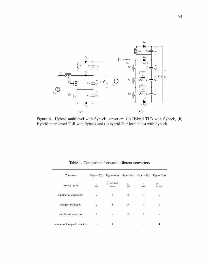
94
D1
+
Vo
_
RQ1
VinQ2 C2
D2
C1
iin
C3
D3
N1
N2
+
vC1_
+
vC2_
+
vC3_
(a)
D1
+
Vo
_
R
Q1
Vin
Q2 C2
C1
iin
C4
D3
C3Q3
D4
+
vC4_
+
vC1_
+
vC2_
+
vC3_
_ vD1 +
+ vD4 _
N1
N2
(b)
Q4
Q5
Figure 6. Hybrid multilevel with flyback converter: (a) Hybrid TLB with flyback, (b)Hybrid interleaved TLB with flyback and (c) hybrid four-level boost with flyback
Table 1. Comparison between different converters
Converter Figure 2(a) Figure 6(a) Figure 4(a) Figure 5(a) Figure 3(a)
Voltage gain 11−d
N2N1(2d−1)+22(1−d)
2d1−d
21−d
N2N1
11−d
Number of capacitors 2 3 2 3 2
Number of diodes 2 3 5 4 4
number of inductors 1 − 2 2 −
number of Coupled inductors − 1 − − 1
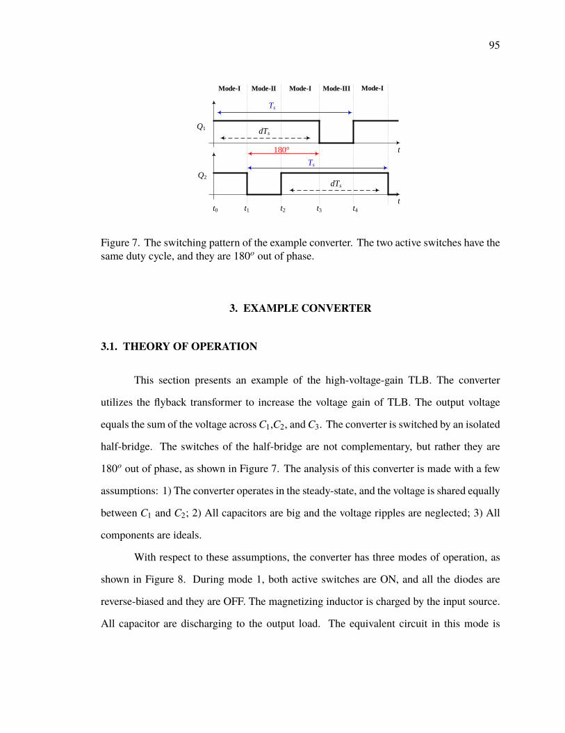
95
Mode-I
Q1
Q2
Mode-I Mode-II Mode-III
t
t
Ts
Ts
dTs
Mode-I
t0 t1 t2 t3 t4
180°
dTs
Figure 7. The switching pattern of the example converter. The two active switches have thesame duty cycle, and they are 180o out of phase.
3. EXAMPLE CONVERTER
3.1. THEORY OF OPERATION
This section presents an example of the high-voltage-gain TLB. The converter
utilizes the flyback transformer to increase the voltage gain of TLB. The output voltage
equals the sum of the voltage across C1,C2, and C3. The converter is switched by an isolated
half-bridge. The switches of the half-bridge are not complementary, but rather they are
180o out of phase, as shown in Figure 7. The analysis of this converter is made with a few
assumptions: 1) The converter operates in the steady-state, and the voltage is shared equally
between C1 and C2; 2) All capacitors are big and the voltage ripples are neglected; 3) All
components are ideals.
With respect to these assumptions, the converter has three modes of operation, as
shown in Figure 8. During mode 1, both active switches are ON, and all the diodes are
reverse-biased and they are OFF. The magnetizing inductor is charged by the input source.
All capacitor are discharging to the output load. The equivalent circuit in this mode is

96
D1
+
Vo
_
RQ1
VinQ2 C2
D2
C1
iin
C3
D3
N2
N1
Lm +
vC1_
+
vC2_
+
vC3_
_ vD3 +
_ vD1 +
+ vD2 _
D1
+
Vo
_
RQ1
VinQ2 C2
D2
C1
iin
C3
D3
N1
N2
Lm +
vC1_
+
vC2_
+
vC3_
_ vD3 +
_ vD1 +
+ vD2 _
D1
+
Vo
_
RQ1
VinQ2 C2
D2
C1
iin
C3
D3
N2
N1
Lm +
vC1_
+
vC2_
+
vC3_
_ vD3 +
_ vD1 +
+ vD2 _
(a)
(b)
(c)
Figure 8. Modes of operation: a) mode 1: Q1 and Q2 are ON, b) mode 2: Q1 is ON and Q2is OFF and c) mode 3: Q1 is OFF and Q2 is ON
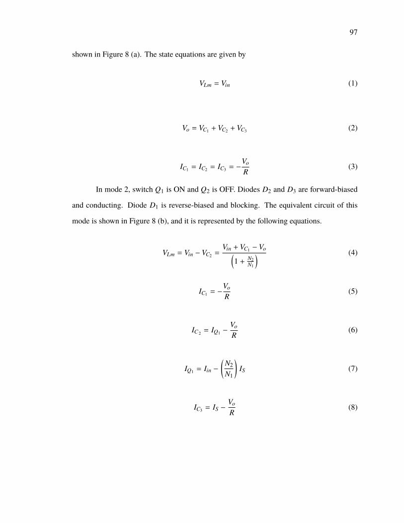
97
shown in Figure 8 (a). The state equations are given by
VLm = Vin (1)
Vo = VC1 + VC2 + VC3 (2)
IC1 = IC2 = IC3 = −Vo
R(3)
In mode 2, switch Q1 is ON and Q2 is OFF. Diodes D2 and D3 are forward-biased
and conducting. Diode D1 is reverse-biased and blocking. The equivalent circuit of this
mode is shown in Figure 8 (b), and it is represented by the following equations.
VLm = Vin − VC2 =Vin + VC1 − Vo(
1 + N2N1
) (4)
IC1 = −Vo
R(5)
IC2 = IQ1 −Vo
R(6)
IQ1 = Iin −
(N2N1
)IS (7)
IC3 = IS −Vo
R(8)
98
In mode 3, switch Q1 is OFF and Q2 is ON. The diode D2 is reverse-biased and
blocking. The other diodes are forward-biased and conducting. Figure 8 (c) shows the
equivalent circuit of this mode. The state equations of this mode are given by
VLm = Vin − VC1 =Vin + VC2 − Vo(
1 + N2N1
) (9)
IC1 = IQ2 −Vo
R(10)
IQ2 = Iin −
(N2N1
)IS (11)
IC2 = −Vo
R(12)
IC3 = IS −Vo
R(13)
By applying volt-second balance, one can obtain the steady state equations across the output
capacitors, as follows:
VC1 = VC2 =0.5 Vin
1 − d(14)
VC3 =
N2N1(2d − 1)
2(1 − d)× Vin (15)
The ideal voltage gain of the proposed converter is given by
M =Vo
Vin=
N2N1(2d − 1) + 22(1 − d)
(16)
The gain is a function of the duty and turns ratio. Figure 9 shows the gain of the proposed
converter. Also, the gain is compared to the converter listed in Table 1, as shown in Figure 10
99
Figure 9. Gain of the converter
duty ratio0.5 0.55 0.6 0.65 0.7 0.75 0.8 0.85 0.9 0.95
0
5
10
15
20
25
30
35
40
Fig. 2(a)
Fig. 3(a)
Fig. 4(a)
Fig. 5(a)
Fig. 6(a)
Volt
age
gai
n
Figure 10. Voltage gain of the converters listed in Table. 1

100
4. COMPONENT SELECTIONS AND EFFICIENCY ANALYSIS
This section present design information of the example converter and component
selections.
4.1. ACTIVE SWITCHES
The voltage stress across the active switches is the same as that of the TLB converter,
which is half of the CBC. The voltage stress can be calculated by
VQ1 = VQ2 =0.5Vin
1 − d(17)
The average current of the MOSFETs is given by
IQ1,avg = IQ2,avg = Iin ×
N2N1(2d − 1) + 2d
N2N1(2d − 1) + 2
(18)
where Iin can be obtained using the following equation
Iin,avg = Io ×
N2N1(2d − 1) + 22(1 − d)
(19)
The peak values of the active switches and the peak value of the input current are
the same, and they are equal to
Iin,pk = IQ1,pk = IQ2,pk = Iin,avg +Vin(2d − 1)
2 fsLm(20)
The rms current is approximated by
IQ1,rms =
√(Io
N2N1(2d−1)+2d
N2N1(2d−1)+2
N2N1(2d−1)+22(1−d) )
2 + Io
N2N1(2d−1)+22(1−d)
Vin(2d−1)fsLm
+ (Vin(2d−1)√
3 fsLm)2 (21)
and IQ1,rms = IQ2,rms if the voltage across C2 and C1 is equal.

101
4.2. DIODES
The voltage stress of the diodes D1 and D2 can be calculated using
VD1 = VD2 =0.5Vin
1 − d(22)
the stress on the output diode D3 is given by
VD3 =0.5 N2
N1Vin
1 − d(23)
The average current for all the diodes is equal and given by
ID1,avg = ID2,avg = ID3,avg = Io (24)
However, the RMS current values are different for D3 than they are for D1 and D2. The
RMS current is approximated by
ID1,rms = ID2,rms =Io
√1 − d
(25)
ID3,rms =Io√
2(1 − d)(26)
4.3. CAPACITORS
The capacitors’ voltages were already mentioned in the steady-state section, and,
based on that, the voltage rating of the capacitors is selected. The capacitance is selected
based on the tolerated voltage ripple of the output voltage. The capacitance can be calculated
by
C = Iod
∆v × fs(27)

102
Note that the frequency seen by C3 is twice that of the switching frequency. Hence, the
required capacitance is reduced to half. The effective values of the capacitor currents are
approximated by
IC1,rms = IC2,rms = Io
√d
1 − d(28)
IC3,rms = Io
√2d − 1
2(1 − d)(29)
4.4. COUPLED INDUCTORS
The turns ratio of the coupled inductors can be calculated using
N2N1= 2 ×
Vo
Vin(1 − d) − 12d − 1
(30)
Note that d is higher than 0.5. The magnetizing inductance can be designed based on the
tolerated current ripple which is given by
Lm =Vin(2d − 1)
2∆i fs(31)
where ∆i is the tolerated current ripple, which is usually 20 − 30% of the average current.
4.5. THE LOSS ANALYSIS
The losses of the converter can be divided by the losses in each component. The
losses in the coupled inductor are given by
PL = I2in,rms × Rdc︸ ︷︷ ︸copper loss
+ KFe
(dVin
2 fsN1 Ac
) β(core volume)︸ ︷︷ ︸
core loss
(32)

103
where Rdc is the dc resistance of the copper wire. The parameters KFe and β are
related to the core loss and determined from the manufacturer’s datasheet [30]. N1 is the
number of primary turns, and Ac is the cross section area of the core. The loss in both
MOSFETs is given by
PQ,total = 2 (I2
Q,rmsRon)︸ ︷︷ ︸
conduction loss
+ IQ,avgVQ(to f f + ton) fs︸ ︷︷ ︸overlap loss
+ CossVQ2 fs︸ ︷︷ ︸
loss caused byCoss discharge
(33)
where Rds(on) is the on-state resistance of theMOSFET, ton and to f f are the turn-ON
and turn-OFF times, respectively, and the Coss is the output capacitance of the MOSFET.
Diode conduction loss is given by
PD = VF × Io︸ ︷︷ ︸conduction
+ QR×Vr× fs︸ ︷︷ ︸reverse recovery loss
(34)
where VF is the forward voltage of the diode, QR is the reverse recovery charge,
and Vr is the maximum reverse voltage. The losses caused by the capacitors’ equivalent
series resistance (ESR) is not significant compared to the aforementioned losses. The losses
caused by ESR are given by
PC = I2C,rmsESR (35)
The loss distribution and efficiency analysis are given in the next sections.
5. SIMULATION
The proposed converter was simulated using Simulink with PLECS blockset. The
parameters used in the simulation are listed in Table 2, and small parasitic elements were
included to help the solver avoid singular loops. The voltages and currents for the switches
are shown in Figure 11. The maximum voltage stress across the active switches is 56 V ,
and that is also the maximum voltage across diodes D1 and D2. However, diode D3 has to
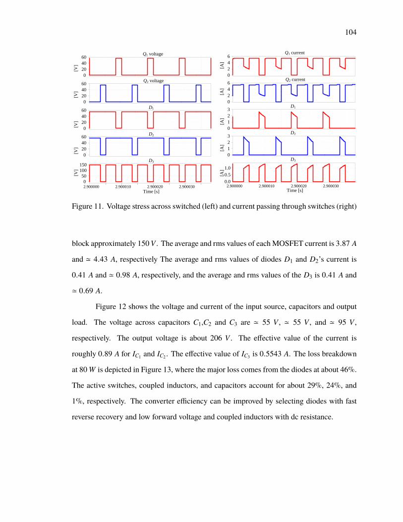
104
Time [s]2.900000 2.900010 2.900020 2.900030
Q1 current
Q2 current
D1
D2
D3
0
2
4
6
0
2
4
6
0
1
2
3
0
1
2
3
0.0
0.5
1.0
Q1 voltage
Q2 voltage
D1
D2
D3
0
20
40
60
0
20
40
60
0
20
40
60
0
20
40
60
Time [s]2.900000 2.900010 2.900020 2.900030
0
50
100
150
[A]
[A]
[A]
[A]
[A]
[V]
[V]
[V]
[V]
[V]
Figure 11. Voltage stress across switched (left) and current passing through switches (right)
block approximately 150 V . The average and rms values of eachMOSFET current is 3.87 A
and ' 4.43 A, respectively The average and rms values of diodes D1 and D2’s current is
0.41 A and ' 0.98 A, respectively, and the average and rms values of the D3 is 0.41 A and
' 0.69 A.
Figure 12 shows the voltage and current of the input source, capacitors and output
load. The voltage across capacitors C1,C2 and C3 are ' 55 V , ' 55 V , and ' 95 V ,
respectively. The output voltage is about 206 V . The effective value of the current is
roughly 0.89 A for IC1 and IC2 . The effective value of IC3 is 0.5543 A. The loss breakdown
at 80 W is depicted in Figure 13, where the major loss comes from the diodes at about 46%.
The active switches, coupled inductors, and capacitors account for about 29%, 24%, and
1%, respectively. The converter efficiency can be improved by selecting diodes with fast
reverse recovery and low forward voltage and coupled inductors with dc resistance.

105
0
5
10
0
1
2
0
1
2
-0.5
0.0
0.5
1.0
Time [s]2.900000 2.900010 2.900020 2.900030
× 1e-1
4.10
4.15
Vin
VC1
15
20
25
50
55
60
50
55
60
90
95
100
Time [s]2.90000 2.90010 2.90020 2.90030
150
200
250
VC2
VC3
VCo
Iin
IC1
IC2
IC3
ICo
[A]
[A]
[A]
[A]
[A]
[V]
[V]
[V]
[V]
[V]
Figure 12. Input, output and capacitors waveforms. The voltage waveforms (left) andcurrent waveforms (right)
Diodes
MOSFETs
Coupled inductors
Capacitors
Figure 13. Simulated loss breakdown at 80 W

106
Table 2. List of parameters used in the simulation
Parameter Value
Turns ratio 2.7
Lm 500 µH
Vin 20 V
Vo 200 V
Load R 500 Ω
Duty cycle 0.82
fs 100 kHz
Capacitors 30 µF
5.1. PHOTOVOLTAIC SOURCE SIMULATION
The PV module (Uni-solar PVL-136) used in this simulation is made of a triple-
junction amorphous silicon (3 − a − Si) material. The nominal efficiency of the module is
roughly 6.26 %, and the area of the module is about 2.16 m2. The electrical characteristics
of the PV panel are given in Table 3 [31]. The simulation of a PV panel requires the
identification of several PV parameters, such as the series resistance Rs, parallel resistance
Rsh, ideality factor n, saturation current Is and photocurrent Iph. One can extract the
parameters of a single diode model using different methods, such as in [32]. Table. 4 lists
the extracted parameters using various approaches. The IV and PV characteristic curves
at the 1000 W/m2 and 25C are shown in Figure 14. The fill factor of the module is
0.574. Plotting the I-V and P-V curves at different temperature values and irradiance levels
illustrates how the output power of the PV panel is affected. Figure 15 shows the effect of
the temperature on the output power. The PV panel has a lower open circuit Voc at a higher
temperature. The output power is also reduced as the temperature is increased. Figure 16
illustrates the correlation between the irradiance and the output power. The output power
of the PV increases as the solar irradiance increases [35].
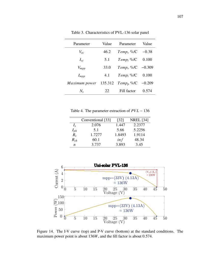
107
Table 3. Characteristics of PVL-136 solar panel
Parameter Value Parameter Value
Voc 46.2 Tempv %/C −0.38
Isc 5.1 Tempi %/C 0.100
Vmpp 33.0 Tempv %/C −0.309
Impp 4.1 Tempi %/C 0.100
Maximum power 135.312 Tempp %/C −0.209
Ns 22 Fill factor 0.574
Table 4. The parameter extraction of PV L − 136
Conventional [33] [32] NREL [34]Is 2.076 1.447 2.2377Iph 5.1 5.66 5.2256Rs 1.7277 1.8493 1.9114Rsh 60.1 in f 48.34n 3.737 3.893 3.45
Voltage (V)0 5 10 15 20 25 30 35 40 45 50
Curr
ent (A
)
0
2
4
6 Uni-solar PVL-136
Voltage (V)0 5 10 15 20 25 30 35 40 45 50
Pow
er (W
)
0
50
100
150
mpp=(33V) (4.13A)
136W
(Voc) (Isc)
236W
mpp=(33V) (4.13A)
136W
Figure 14. The I-V curve (top) and P-V curve (bottom) at the standard conditions. Themaximum power point is about 136W , and the fill factor is about 0.574.

108
Voltage (V)0 5 10 15 20 25 30 35 40 45 50
Curr
ent (A
)
0
2
4
6
45 oC
25 oC
Uni-solar PVL-136
Voltage (V)0 5 10 15 20 25 30 35 40 45 50
Pow
er (W
)
0
50
100
150
45 oC
25 oC
Figure 15. Temperature’s effect on the I-V and P-V curves. As the temperature increases,the output power of the PV is reduced.
Voltage (V)0 5 10 15 20 25 30 35 40 45 50C
urr
ent (A
)
0
2
4
6 1 kW/m2
0.5 kW/m2
0.1 kW/m2
Module type: Uni-solar PVL-136
Voltage (V)0 5 10 15 20 25 30 35 40 45 50
Pow
er (W
)
0
50
100
1501 kW/m2
0.5 kW/m2
0.1 kW/m2
Figure 16. Irradiance’s effect on the output of the PV panel. The figure shows that there isa strong correlation between the current of the PV panel and the irradiance level.
109
5.2. MPPT CONTROL
The PV panel operates at the maximum power (MPP) if the load resistance matches
the PV resistance of the maximum power point (Rmpp). Often the load resistance does not
match the PV, and that results in a power decrease. Therefore, a maximum power point
tracker (MPPT) is needed to ensure that the PV panel produces the maximum point at any
solar irradiance level. Although there are plenty of MPPT algorithms and techniques [36–
40], perturb and observe (P&O) is the simplest and most widely used. The flow chart of
P&O is shown in Figure 17. The challenge with such an algorithm is the size of the step of
the duty. A large step size can reach the vicinity of MPP faster but mightcause the tracker
to zigzag, resulting in an inablity to reach the true MPP. Small step sizes can reacher closer
operation points near the true MPP but take more time to reach the MPP, and in the case of
local and global maxima, the converter might get stuck in a local maxima. Several solutions
suggest the adaptive or variable step size [41], in which the step size can be large if the
converter operates far from the MPP and small once it operates near the MPP. However,
in rapid changes of the solar irradiance level, the controller might not perform correctly.
Figure 18 shows the effect of the step size on the algorithm performance. The converter
was simulated to interface three parallel-connected solar panels. The simulation results are
shown in Figure 19. The controller can extract the maximum power output of the PV system
and perform well in cases where there is a huge dip in the solar irradiance.
6. EXPERIMENTAL
This section presents the implementation of the hardware prototype and the experi-
mental results of the example converter. An 80 W hardware prototype, shown in Figure 20,
was implemented to verify the analysis and simulation. The components used to implement
the hardware are listed in Table 5. The voltage stress across components, capacitor voltages,
and output voltages are depicted in Figures. 21, 22, and 22, respectively. The output voltage
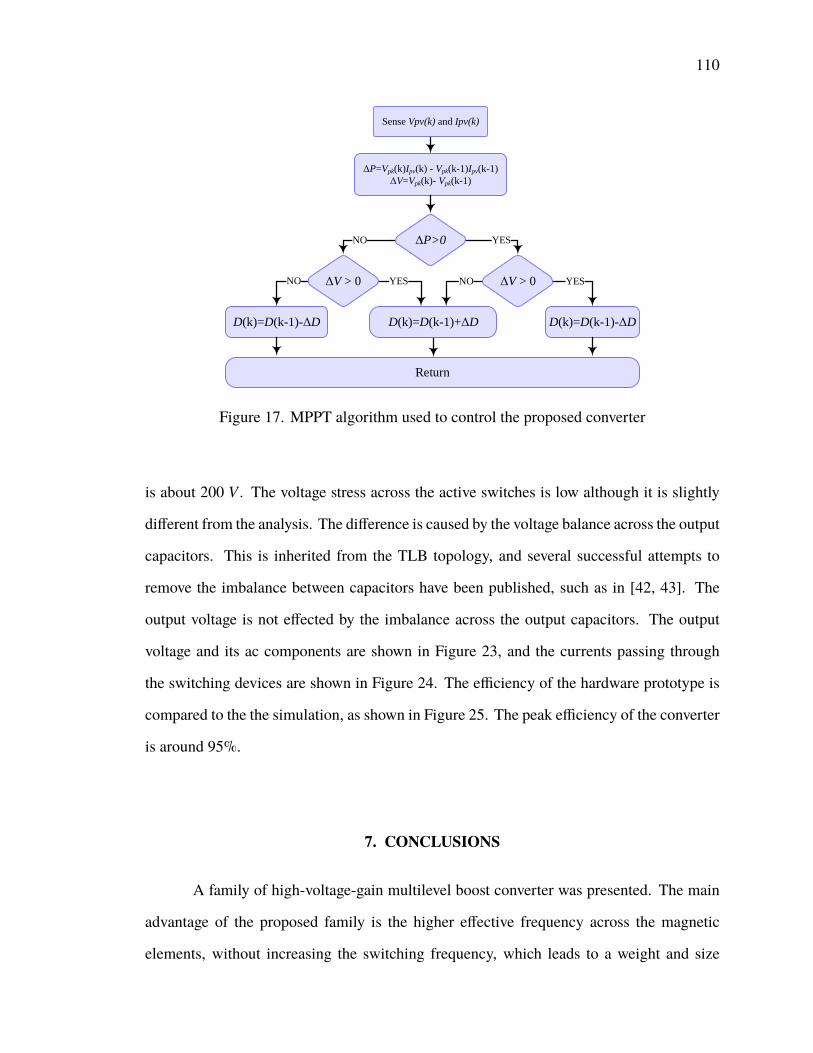
110
NO
Sense Vpv(k) and Ipv(k)
ΔP>0
ΔP=Vpk(k)Ipv(k) - Vpk(k-1)Ipv(k-1)
ΔV=Vpk(k)- Vpk(k-1)
ΔV > 0
NO YES
D(k)=D(k-1)-ΔD
NO YES
D(k)=D(k-1)-ΔDD(k)=D(k-1)+ΔD
YES
Return
ΔV > 0
Figure 17. MPPT algorithm used to control the proposed converter
is about 200 V . The voltage stress across the active switches is low although it is slightly
different from the analysis. The difference is caused by the voltage balance across the output
capacitors. This is inherited from the TLB topology, and several successful attempts to
remove the imbalance between capacitors have been published, such as in [42, 43]. The
output voltage is not effected by the imbalance across the output capacitors. The output
voltage and its ac components are shown in Figure 23, and the currents passing through
the switching devices are shown in Figure 24. The efficiency of the hardware prototype is
compared to the the simulation, as shown in Figure 25. The peak efficiency of the converter
is around 95%.
7. CONCLUSIONS
A family of high-voltage-gain multilevel boost converter was presented. The main
advantage of the proposed family is the higher effective frequency across the magnetic
elements, without increasing the switching frequency, which leads to a weight and size
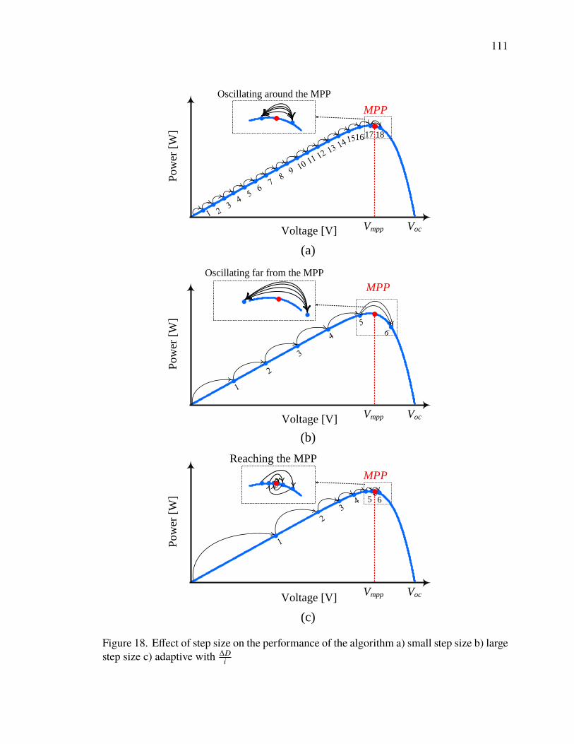
111
Po
wer
[W
]
Voltage [V] VocVmpp
MPP
Oscillating around the MPP
1617 18
Po
wer
[W
]
Voltage [V] VocVmpp
MPP
Oscillating far from the MPP
Po
wer
[W
]
Voltage [V]VocVmpp
MPP
Reaching the MPP
5 6
(a)
(b)
(c)
Figure 18. Effect of step size on the performance of the algorithm a) small step size b) largestep size c) adaptive with ∆D
i

112
Figure 19. The simulated results of the converter with MPPT: a) Performance of thecontroller b) Solar irradiance
Figure 20. Hardware prototype
Table 5. Component Listing for the Hardware Prototype
Item Designation Rating Part No.
Coupled inductors N2N1= 2.7 200 µH, ET D 49, turns ratio= 2.7
Capacitor C1,C2C3
10 µF B32674D3106K
MOSFET Q1,Q2150 V,37 A
Rds(on) = 10.525 mΩ IPA105N15N3
Diode D1,D2D3
250V,40AVF = 0.86 V, trr = 35 ns MBR40250G
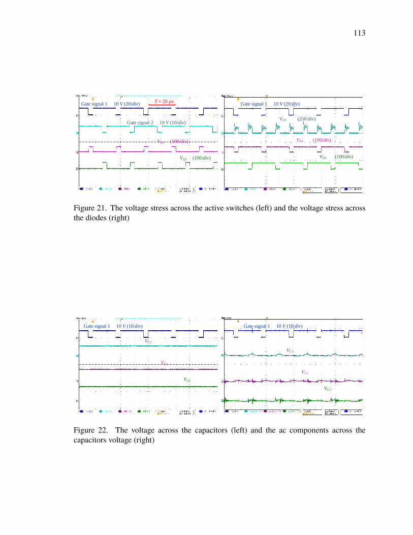
113
Gate signal 1 10 V (20/div)
Gate signal 2 10 V (10/div)
T = 20 µs Gate signal 1 10 V (20/div)
VQ2 (100/div)
VQ1 (100/div)
VD3 (250/div)
VD2 (100/div)
VD1 (100/div)
Figure 21. The voltage stress across the active switches (left) and the voltage stress acrossthe diodes (right)
Gate signal 1 10 V (10/div) Gate signal 1 10 V (10/div)
VC3
VC2
VC1
VC3
VC2
VC1
Figure 22. The voltage across the capacitors (left) and the ac components across thecapacitors voltage (right)

114
Gate signal 1 10 V (10/div)
Vo = 200 V (100/div)
ΔVo < 0.99 V (5/div)
Figure 23. Experimental results of the output voltage and the voltage ripple across theoutput voltage
Gate signal 1 10 V (10/div) Gate signal 1 10 V (10/div)
IQ2
IQ1
ID3
ID2
ID1
Iin
Figure 24. Input current and active switch currents (left) and diodes currents (right)
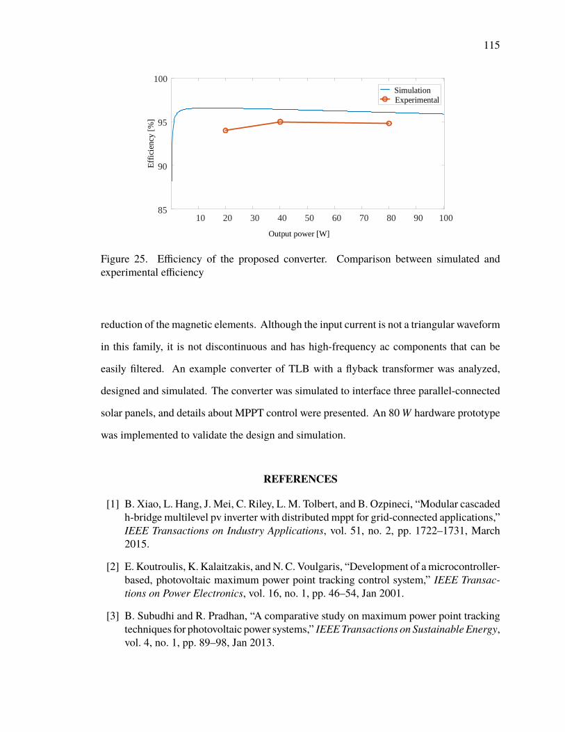
115
10 20 30 40 50 60 70 80 90 10085
90
95
100
Simulation
Experimental
Output power [W]
Eff
icie
ncy
[%
]
Figure 25. Efficiency of the proposed converter. Comparison between simulated andexperimental efficiency
reduction of the magnetic elements. Although the input current is not a triangular waveform
in this family, it is not discontinuous and has high-frequency ac components that can be
easily filtered. An example converter of TLB with a flyback transformer was analyzed,
designed and simulated. The converter was simulated to interface three parallel-connected
solar panels, and details about MPPT control were presented. An 80 W hardware prototype
was implemented to validate the design and simulation.
REFERENCES
[1] B. Xiao, L. Hang, J. Mei, C. Riley, L. M. Tolbert, and B. Ozpineci, “Modular cascadedh-bridge multilevel pv inverter with distributed mppt for grid-connected applications,”IEEE Transactions on Industry Applications, vol. 51, no. 2, pp. 1722–1731, March2015.
[2] E. Koutroulis, K. Kalaitzakis, andN. C. Voulgaris, “Development of amicrocontroller-based, photovoltaic maximum power point tracking control system,” IEEE Transac-tions on Power Electronics, vol. 16, no. 1, pp. 46–54, Jan 2001.
[3] B. Subudhi and R. Pradhan, “A comparative study on maximum power point trackingtechniques for photovoltaic power systems,” IEEETransactions on Sustainable Energy,vol. 4, no. 1, pp. 89–98, Jan 2013.

116
[4] G. R. Walker and P. C. Sernia, “Cascaded dc-dc converter connection of photovoltaicmodules,” IEEE transactions on power electronics, vol. 19, no. 4, pp. 1130–1139,2004.
[5] G. M. Masters, Renewable and efficient electric power systems. John Wiley & Sons,2013.
[6] J.-M. Kwon, K.-H. Nam, and B.-H. Kwon, “Photovoltaic power conditioning systemwith line connection,” IEEE Transactions on Industrial Electronics, vol. 53, no. 4, pp.1048–1054, 2006.
[7] F. L. Tofoli, D. de Castro Pereira, W. J. de Paula, and D. d. S. O. Júnior, “Survey onnon-isolated high-voltage step-up dc–dc topologies based on the boost converter,” IETpower Electronics, vol. 8, no. 10, pp. 2044–2057, 2015.
[8] S.-M. Chen, T.-J. Liang, L.-S. Yang, and J.-F. Chen, “A cascaded high step-up dc–dc converter with single switch for microsource applications,” IEEE Transactions onPower Electronics, vol. 26, no. 4, pp. 1146–1153, 2011.
[9] C. Carvalho, J. P. Oliveira, and N. Paulino, “Survey and analysis of the design issuesof a low cost micro power dc-dc step up converter for indoor light energy harvestingapplications,” in Proceedings of the 19th International Conference Mixed Design ofIntegrated Circuits and Systems - MIXDES 2012, May 2012, pp. 455–460.
[10] H. C. Sartori, F. Beltrame, M. L. Martins, J. E. Baggio, and J. R. Pinheiro, “Evaluationof an optimal design for a single-phase boost pfc converter (ccm) considering differentmagnetic materials core,” in Power Electronics Conference (COBEP), 2013 Brazilian.IEEE, 2013, pp. 1304–1310.
[11] F. Z. Peng, M. L. Gebben, and B. Ge, “A compact nx dc-dc converter for photovoltaicpower systems,” in Energy Conversion Congress and Exposition (ECCE), 2013 IEEE.IEEE, 2013, pp. 4780–4784.
[12] J. Leyva-Ramos, M. Ortiz-Lopez, L. Diaz-Saldierna, andM.Martinez-Cruz, “Averagecurrent controlled switching regulators with cascade boost converters,” IET powerelectronics, vol. 4, no. 1, pp. 1–10, 2011.
[13] A. A. A. Freitas, F. L. Tofoli, E. M. S. Júnior, S. Daher, and F. L. M. Antunes, “High-voltage gain dc–dc boost converter with coupled inductors for photovoltaic systems,”IET Power Electronics, vol. 8, no. 10, pp. 1885–1892, 2015.
[14] D. G. Holmes and T. A. Lipo, Pulse width modulation for power converters: principlesand practice. John Wiley & Sons, 2003, vol. 18.
[15] M. K. Kazimierczuk, Pulse-width modulated DC-DC power converters. John Wiley& Sons, 2015.
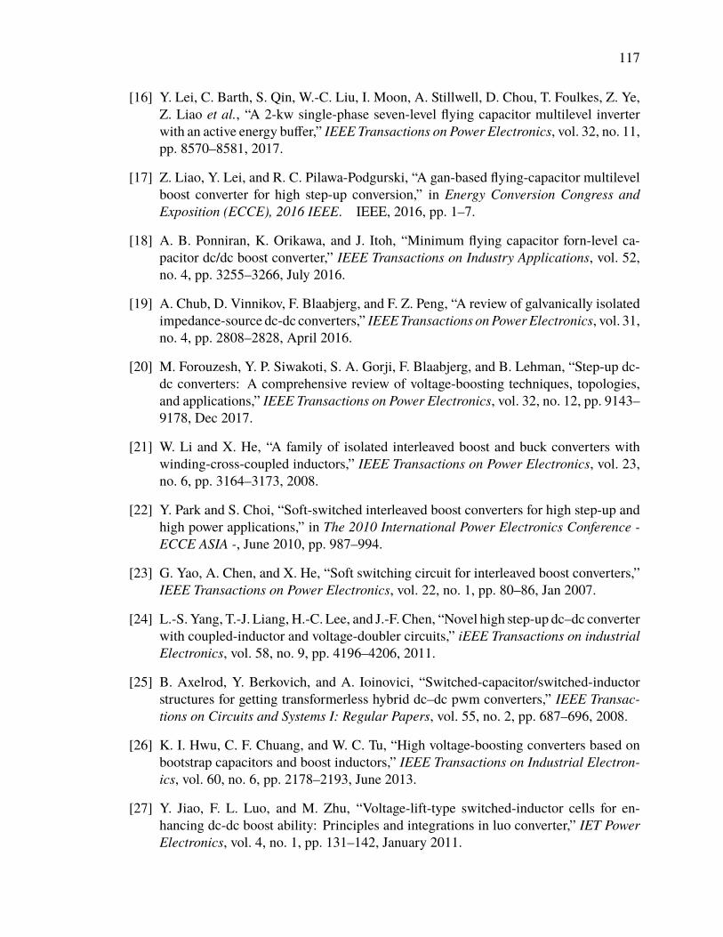
117
[16] Y. Lei, C. Barth, S. Qin, W.-C. Liu, I. Moon, A. Stillwell, D. Chou, T. Foulkes, Z. Ye,Z. Liao et al., “A 2-kw single-phase seven-level flying capacitor multilevel inverterwith an active energy buffer,” IEEE Transactions on Power Electronics, vol. 32, no. 11,pp. 8570–8581, 2017.
[17] Z. Liao, Y. Lei, and R. C. Pilawa-Podgurski, “A gan-based flying-capacitor multilevelboost converter for high step-up conversion,” in Energy Conversion Congress andExposition (ECCE), 2016 IEEE. IEEE, 2016, pp. 1–7.
[18] A. B. Ponniran, K. Orikawa, and J. Itoh, “Minimum flying capacitor forn-level ca-pacitor dc/dc boost converter,” IEEE Transactions on Industry Applications, vol. 52,no. 4, pp. 3255–3266, July 2016.
[19] A. Chub, D. Vinnikov, F. Blaabjerg, and F. Z. Peng, “A review of galvanically isolatedimpedance-source dc-dc converters,” IEEETransactions onPowerElectronics, vol. 31,no. 4, pp. 2808–2828, April 2016.
[20] M. Forouzesh, Y. P. Siwakoti, S. A. Gorji, F. Blaabjerg, and B. Lehman, “Step-up dc-dc converters: A comprehensive review of voltage-boosting techniques, topologies,and applications,” IEEE Transactions on Power Electronics, vol. 32, no. 12, pp. 9143–9178, Dec 2017.
[21] W. Li and X. He, “A family of isolated interleaved boost and buck converters withwinding-cross-coupled inductors,” IEEE Transactions on Power Electronics, vol. 23,no. 6, pp. 3164–3173, 2008.
[22] Y. Park and S. Choi, “Soft-switched interleaved boost converters for high step-up andhigh power applications,” in The 2010 International Power Electronics Conference -ECCE ASIA -, June 2010, pp. 987–994.
[23] G. Yao, A. Chen, and X. He, “Soft switching circuit for interleaved boost converters,”IEEE Transactions on Power Electronics, vol. 22, no. 1, pp. 80–86, Jan 2007.
[24] L.-S. Yang, T.-J. Liang, H.-C. Lee, and J.-F. Chen, “Novel high step-up dc–dc converterwith coupled-inductor and voltage-doubler circuits,” iEEE Transactions on industrialElectronics, vol. 58, no. 9, pp. 4196–4206, 2011.
[25] B. Axelrod, Y. Berkovich, and A. Ioinovici, “Switched-capacitor/switched-inductorstructures for getting transformerless hybrid dc–dc pwm converters,” IEEE Transac-tions on Circuits and Systems I: Regular Papers, vol. 55, no. 2, pp. 687–696, 2008.
[26] K. I. Hwu, C. F. Chuang, and W. C. Tu, “High voltage-boosting converters based onbootstrap capacitors and boost inductors,” IEEE Transactions on Industrial Electron-ics, vol. 60, no. 6, pp. 2178–2193, June 2013.
[27] Y. Jiao, F. L. Luo, and M. Zhu, “Voltage-lift-type switched-inductor cells for en-hancing dc-dc boost ability: Principles and integrations in luo converter,” IET PowerElectronics, vol. 4, no. 1, pp. 131–142, January 2011.
118
[28] Y. Tang, D. Fu, T. Wang, and Z. Xu, “Hybrid switched-inductor converters for highstep-up conversion.” IEEE Trans. Industrial Electronics, vol. 62, no. 3, pp. 1480–1490,2015.
[29] T. J. Liang and K. C. Tseng, “Analysis of integrated boost-flyback step-up converter,”IEE Proceedings - Electric Power Applications, vol. 152, no. 2, pp. 217–225, March2005.
[30] R. W. Erickson and D. Maksimovic, Fundamentals of power electronics. SpringerScience & Business Media, 2007.
[31] S. Pacca, D. Sivaraman, and G. A. Keoleian, “Parameters affecting the life cycleperformance of pv technologies and systems,” Energy Policy, vol. 35, no. 6, pp.3316–3326, 2007.
[32] G. Petrone and G. Spagnuolo, “Parameters identification of the single-diode model foramorphous photovoltaic panels,” in 2015 International Conference onCleanElectricalPower (ICCEP), June 2015, pp. 105–109.
[33] J. Merten, J. Asensi, C. Voz, A. Shah, R. Platz, and J. Andreu, “Improved equivalentcircuit and analytical model for amorphous silicon solar cells and modules,” IEEETransactions on electron devices, vol. 45, no. 2, pp. 423–429, 1998.
[34] N. Blair, A. P. Dobos, J. Freeman, T. Neises, M. Wagner, T. Ferguson, P. Gilman, andS. Janzou, “System advisor model, sam 2014.1. 14: General description,” 2014.
[35] H. Patel andV.Agarwal, “Matlab-basedmodeling to study the effects of partial shadingon pv array characteristics,” 2008.
[36] N. Kumar, I. Hussain, B. Singh, and B. K. Panigrahi, “Normal harmonic searchalgorithm based mppt for solar pv system and integrated with grid using reducedsensor approach and pnklms algorithm,” IEEE Transactions on Industry Applications,pp. 1–1, 2018.
[37] T. Esram, J. W. Kimball, P. T. Krein, P. L. Chapman, and P. Midya, “Dynamicmaximumpower point tracking of photovoltaic arrays using ripple correlation control,”IEEE Transactions on power electronics, vol. 21, no. 5, pp. 1282–1291, 2006.
[38] M. Metry, M. B. Shadmand, R. S. Balog, and H. Abu-Rub, “Mppt of photovoltaicsystems using sensorless current-based model predictive control,” IEEE Transactionson Industry Applications, vol. 53, no. 2, pp. 1157–1167, March 2017.
[39] M. Das and V. Agarwal, “Novel high-performance stand-alone solar pv system withhigh-gain high-efficiency dc–dc converter power stages,” IEEE Transactions on In-dustry Applications, vol. 51, no. 6, pp. 4718–4728, Nov 2015.
[40] T. Esram and P. L. Chapman, “Comparison of photovoltaic array maximum powerpoint tracking techniques,” IEEE Transactions on energy conversion, vol. 22, no. 2,pp. 439–449, 2007.
119
[41] F. Liu, S. Duan, F. Liu, B. Liu, and Y. Kang, “A variable step size inc mppt methodfor pv systems,” IEEE Transactions on Industrial Electronics, vol. 55, no. 7, pp.2622–2628, July 2008.
[42] L. A. Vitoi, R. Krishna, D. E. Soman, M. Leijon, and S. K. Kottayil, “Control andimplementation of three level boost converter for load voltage regulation,” in IECON2013 - 39th Annual Conference of the IEEE Industrial Electronics Society, Nov 2013,pp. 561–565.
[43] J. Chen, S. Hou, T. Sun, F. Deng, and Z. Chen, “A new interleaved double-input three-level boost converter,” Journal of Power Electronics, vol. 16, no. 3, pp. 925–935,2016.

120
IV. A FAMILY OF INTERLEAVED STEP-UP TOPOLOGIES USINGSINGLE-SWITCHMULTISTAGE BOOST CONVERTERS AND VOLTAGE
MULTIPLIER CELLS
Ahmad Alzahrani, Pourya Shamsi, and Mehdi Ferdowsi
Departement of Electrical and Computer Engineering
Missouri University of Science and Technology
asakw9, shamsip, [email protected]
ABSTRACT
This paper presents an interleaved step-up dc-dc converter with single-switch mul-
tistage boost converters and voltage multiplier cells (VMC) to convert input sources that
have low output voltage, such as renewable energy sources, to a high-voltage dc bus. The
proposed converter features low voltage stress across the components, equal current sharing
among all phases, and a smooth input current. Moreover, the proposed converter has a
modular structure in both the VMC and the boost stage. That is, the VMC can have N
number of cells, and the boost stage can have k number of stages. The k can be different
in each phase, which allows the designers to integrate two independent renewable energy
sources that have different output voltages. The converter was analyzed, and details about
the design are included. An 80 W hardware prototype was implemented to validate the
theory of operation and analysis.
Keywords: DC-DC, Interleaved, High-Gain, Multilevel, Quadratic, PV, Renewable, Power
electronics, Voltage multiplier cells

121
1. INTRODUCTION
The high-voltage-gain dc-dc step-up converters have become more popular in recent
years due to the progress in power and energy fields and the emergence and development
of technologies and applications, such as dc microgrids and dc distribution systems [1–5].
The dc distribution system was found to be an enhanced alternative to the ac distribution
system due to the low number of conversions, protections against grounding faults, high
power quality, and cost. More importantly, the dc distribution is suitable for integrating
renewable energy sources [6–12]. However, most of the renewable energy sources have
low output voltage, which needs to be boosted by about 15 − 25 times. The most common
topology used for stepping up the voltage is the conventional boost converter, which has
a simple structure and a low number of components. However, the voltage gain of the
conventional boost converter can only be high at extreme duty cycles [13, 14]. Operating at
extremely high duty cycles increases the voltage stress across the components and requires
a large inductance in order to make the converter draw a continuous input current. With
consideration of the conduction and the switching loss, the voltage gain is significantly
reduced. Such drawbacks sparked the research for a topology with high-voltage-gain
conversion ratio.
One way to increase the voltage gain is by cascading multiple conventional boost
converters, where the output voltage is increased exponentially. Cascading two conventional
boost converters allows both stages to operate at a low duty cycle [15–17]. Therefore, the
voltage stress on the first stage components is low. However, the stress on the second stage
output diode still has to block the output voltage. The quadratic converter can be simplified
by using only a single active switch. The output diode of such a converter suffers from
high voltage stress, and the input current has high current ripples [18–20]. The voltage
stress across the components is reduced in the three-level boost converter, and the size of
the converter is decreased due to the increase of the effective frequency across the inductor.
The three-level boost has the same gain as the boost converter, which is not sufficient
122
for renewable energy applications [21, 22]. Switched capacitor circuits are capable of
increasing the voltage gain by increasing the number of switching cells. Several advantages
can be obtained: high power density, low EMI, the capability of being fabricated into IC
chips. The drawbacks are the inherent losses, a high number of active switches that require
isolation circuitry and gate drivers. Moreover, the output voltage is fixed and cannot be
regulated. Several topologies utilize the transformer or a coupled inductor’s turns ratio to
increase the voltage gain as in [23–27]. Utilizing the transformer can meet the requirement
of isolation and safety and can provide multiple outputs. However, the power density is
significantly reduced, and the weight of the converter is increased. Also, the stress on the
active switches caused by the parasitic leakage inductance can cause damage to the switches
unless an extra auxiliary circuit is implemented to recycle the energy. Similar to using a
transformer, using an integrated coupled inductor improves the voltage gain but without
providing isolation, such as a hybrid flyback-boost, interleaved with coupled inductors, or
quadratic boost converter with coupled inductors. Such topologies suffer from leakage
inductance as well and require extra circuits for circulating the energy and reducing the
voltage stress across the switches [28–30].
This paper introduces an interleaved single-switch multistage boost converter with
voltage multiplier cells. The converter features low voltage stress on components and high
voltage gain, allows the user to get the most ripple cancellation that interleaving offers, has
the capability to integrate different voltage sources, and can match a wide range of loads.
Each phase of the interleaved multistage can have either the same or a different number of
boost stages than the other phases. This can be very useful for integrating sources with a
significant difference in their output voltage. The VMC stage uses a bi-fold Dickson that
has a symmetrical structure and low voltage stress across the components. Incorporating
two symmetrical phases with the same duty cycle yields equal current sharing between the
phases and a very smooth input current.
The rest of this paper is structured as follows. First, the theory of operation and steady-state
123
analysis of each mode is presented in Section 2. The components selection and design
procedure are presented in Section 3, and the implementation of the hardware prototype
and experimental results are explained in Section 4. Finally, conclusions and future work
are presented in Section 5.
2. THEORY OF OPERATION AND STEADY-STATE ANALYSIS
The general structure of the proposed converter is shown in Figure 1. The converter
consists of two single-switched multistage boost converter cells. These cells are 180 out of
phase, and they are independent of each other, which means each cell can have a different
number of the boost stages, as shown in Figure 1 (b) and (d). Two independent voltage
sources can feed the proposed converter instead of one, which is an essential quality to
interface multiple renewable energy sources. The single switch multistage boost converter
allows the converter to achieve higher converter gain with no need to add extra active
switches and can come in different topologies, as shown in Figure 2. The second stage
of the converter consists of voltage multiplier cells to increase the voltage and reduce the
voltage stress across the diodes. Numerous VMCs can be used with this converter as
in [31–33]. Example converters of the proposed family are shown in Figure 3. In this paper,
Bi-fold Dickson VMC is used for the proposed converter, which features lower stress across
the diodes and capacitors. Therefore, the voltage gain can be increased in three ways: by
increasing the number of VMC cells, by increasing the duty cycle, or by increasing the
number of boost stages. The Figure 4 shows the proposed converter with k boost stages
and N number of VMC cells. The converter can replace all diodes with active switches to
improve the efficiency in case of very high power applications, as shown in Figure 5. The
following analysis and experimentation are based on the converter with k = 2 and N = 2,
as shown in Figure 6. The analysis of the proposed converter was performed on several
assumptions: 1) All components are ideal 2) All capacitors are large so that the voltage is
constant 3) The duty cycles are symmetrical 4) The converter operates in the steady state.
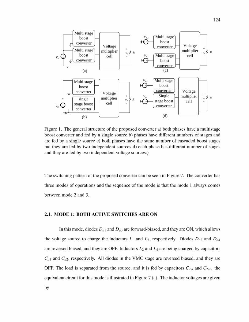
124
Vin
R+
vo _
Multi stage
boost
converterVoltage
multiplier
cell
Multi stage
boost
converter
(a)
(b)
R+
vo _
Voltage
multiplier
cellMulti stage
boost
converter(c)
Multi stage
boost
converter
Vin1 R
+
vo _
Voltage
multiplier
cell
Single
stage boost
converter
(d)
Multi stage
boost
converter
Vin
R
+
vo _
Multi stage
boost
converter Voltage
multiplier
cellsingle
stage boost
converter
Vin2
Vin1
Vin2
Figure 1. The general structure of the proposed converter a) both phases have a multistageboost converter and fed by a single source b) phases have different numbers of stages andare fed by a single source c) both phases have the same number of cascaded boost stagesbut they are fed by two independent sources d) each phase has different number of stagesand they are fed by two independent voltage sources.)
The switching pattern of the proposed converter can be seen in Figure 7. The converter has
three modes of operations and the sequence of the mode is that the mode 1 always comes
between mode 2 and 3.
2.1. MODE 1: BOTH ACTIVE SWITCHES ARE ON
In this mode, diodes Da1 and Da3 are forward-biased, and they are ON, which allows
the voltage source to charge the inductors L1 and L3, respectively. Diodes Da2 and Da4
are reversed biased, and they are OFF. Inductors L2 and L4 are being charged by capacitors
Ca1 and Ca2, respectively. All diodes in the VMC stage are reversed biased, and they are
OFF. The load is separated from the source, and it is fed by capacitors C2A and C2B. the
equivalent circuit for this mode is illustrated in Figure 7 (a). The inductor voltages are given
by
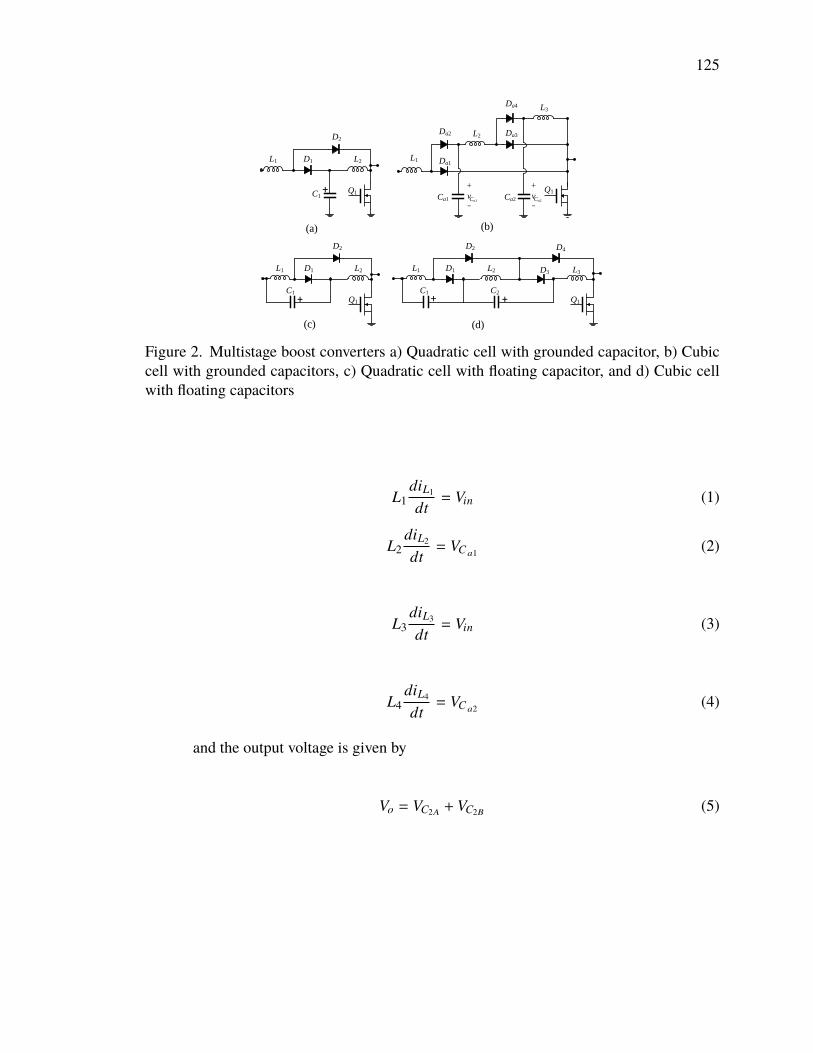
125
D1L1
C1
L2
D2
(a)
D1L1
C1
L2
D2
(b)
D1L1
C1
L2
D2
L3D3
C2
D4
+
+ ++
(c) (d)
Q1
Q1 Q1
Q1
L1
Ca1 Ca2
Da2
Da1
Da4
Da3L2
L3
Ca2
+
v _
Ca1
+
v _
Figure 2. Multistage boost converters a) Quadratic cell with grounded capacitor, b) Cubiccell with grounded capacitors, c) Quadratic cell with floating capacitor, and d) Cubic cellwith floating capacitors
L1diL1
dt= Vin (1)
L2diL2
dt= VC a1 (2)
L3diL3
dt= Vin (3)
L4diL4
dt= VC a2 (4)
and the output voltage is given by
Vo = VC2A + VC2B (5)

126
Q1
R
+
vo _
Co
Q2
Vin
L1
Q1
Q2
C2
+
v _
C2
D1 Do
D2
Vin
C1
+
v _
C1
R
+
vo _
Co
Ca1 Ca2
Ca3 Ca4
Da2
Da1
Da4
Da3
Db1
L2
L3
L4Da5
Da6Da7
Da8
L5
L6Db2
L1
Ca1 Ca2
Ca3 Ca4
Da2
Da1
Da4
Da3L2
L3
L4
L5
L6
Co
R
D1Vo +
Do
C2
(a)
(b)
(c)
Q1
Q2
Vin
L1
Ca1 Ca2
Ca3 Ca4
Da2
Da1
Da4
Da3L2
L3
L4
L5
L6
Ca3
_
v
+
Ca2
+
v _
Ca4
_
v
+
Ca1
+
v _
Ca3
_
v
+
Ca2
+
v _
Ca4
_
v
+
Ca1
+
v _
Ca3
_
v
+
Ca2
+
v _
Ca4
_
v
+
Ca1
+
v _
Da5
Da6Da7
Da8
Da5
Da6Da7
Da8
Figure 3. Different variations of the proposed converter (a) Schematic of the proposedconverter with 3 stages (cubic) and no VMC, (b) another interleaved cubic boost converterwith one stage of cross capacitor VMC, and (c) interleaved cubic boost converter with oneCockcroft-Walton cell.
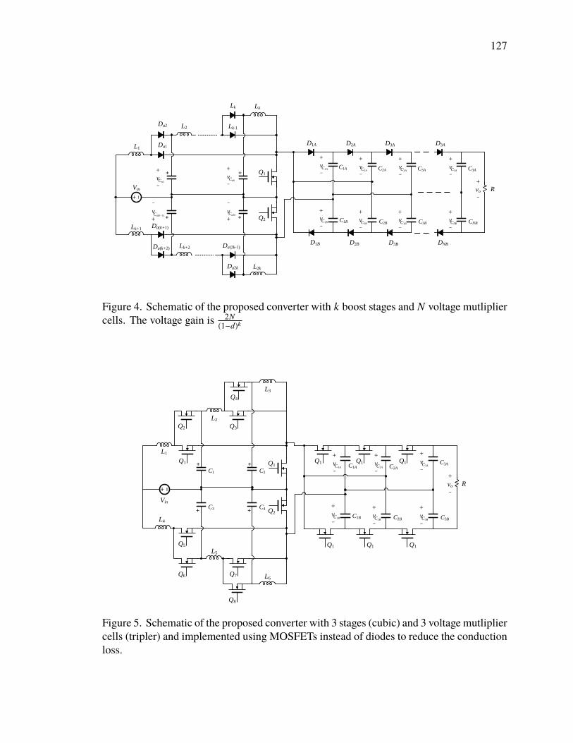
127
Q1
Q2
C3A
+
v _
R
C3A
C3B
+
v _
C3B
C2A
+
v _
C2A
C2B
+
v _
C2B
C1A
+
v _
C1A
C1B
+
v _
C1B
D1A D2A D3A
D1B D2B D3B
+
vo _
Vin
L1
L2
Lk
Lk+1Da(k+1)
L2k
C3A
+
v _
C3A
CNB
+
v _
CNB
D3A
DNB
+
+
+
+
Ca(k+1)
_
v
+Ca2k
_
v
+
Ca1
+
v _
Cak
+
v _
Lk+2
Da2
Da1
Da2k
Da(k+2)Da(2k-1)
Lk
Lk-1
Figure 4. Schematic of the proposed converter with k boost stages and N voltage mutlipliercells. The voltage gain is 2N
(1−d)k
Q1
Q2
Q4
Q3Q2
Q1
Q5
Q6 Q7
Q8
L1
L2
L3
L4
L5
L6
+
+
+
+ C3A
+
v _
R
C3A
C3B
+
v _
C3B
C2A
+
v _
C2A
C2B
+
v _
C2B
C1A
+
v _
C1A
C1B
+
v _
C1B
+
vo _
Q1 Q1 Q1
Q1 Q1 Q1
Vin
C1 C2
C3 C4
Figure 5. Schematic of the proposed converter with 3 stages (cubic) and 3 voltage mutlipliercells (tripler) and implemented using MOSFETs instead of diodes to reduce the conductionloss.

128
Q1
Q1
R
C2A
+
v _
C2A
C2B
+
v _
C2B
C1A
+
v _
C1A
C1B
+
v _
C1B
D1A D2A
D1B D2B
+
vo _
Vin
L1
Ca1
Ca2
Da2
Da1
L2
L3Da3
Da4 L4
Ca1
+
v _
Ca2
_
v
+
Figure 6. Schematic of the proposed converter with k = 2 and N = 2
Q1
Q2
R
C2A
+
v _
C2A
C2B
+
v _
C2B
C1A
+
v _
C1A
C1B
+
v _
C1B
D1A D2A
D1B D2B
+
vo _
Vin
L1
Ca1
Ca2
Da2
Da1
L2
L3Da3
Da4 L5
Q1
Q2
R
C2A
+
v _
C2A
C2B
+
v _
C2B
C1A
+
v _
C1A
C1B
+
v _
C1B
D1A D2A
D1B D2B
+
vo _
Vin
L1
Ca1
Ca2
Da2
Da1
L2
L3Da3
Da4 L4
Q1
Q2
R
C2A
+
v _
C2A
C2B
+
v _
C2B
C1A
+
v _
C1A
C1B
+
v _
C1B
D1A D2A
D1B D2B
+
vo _
Vin
L1
Ca1
Ca2
Da2
Da1
L2
L3Da3
Da4 L4
(a)
(b)
(c)
+
+
+
+
+
+
+
+
+
+
+
+
+
+
+
+
+
+
Figure 7. Equivalent circuits to a) mode 1: both active switches are ON, b) mode 2: Q1 isON and Q2 is OFF, and c) mode 3: Q1 is OFF and Q2 is ON
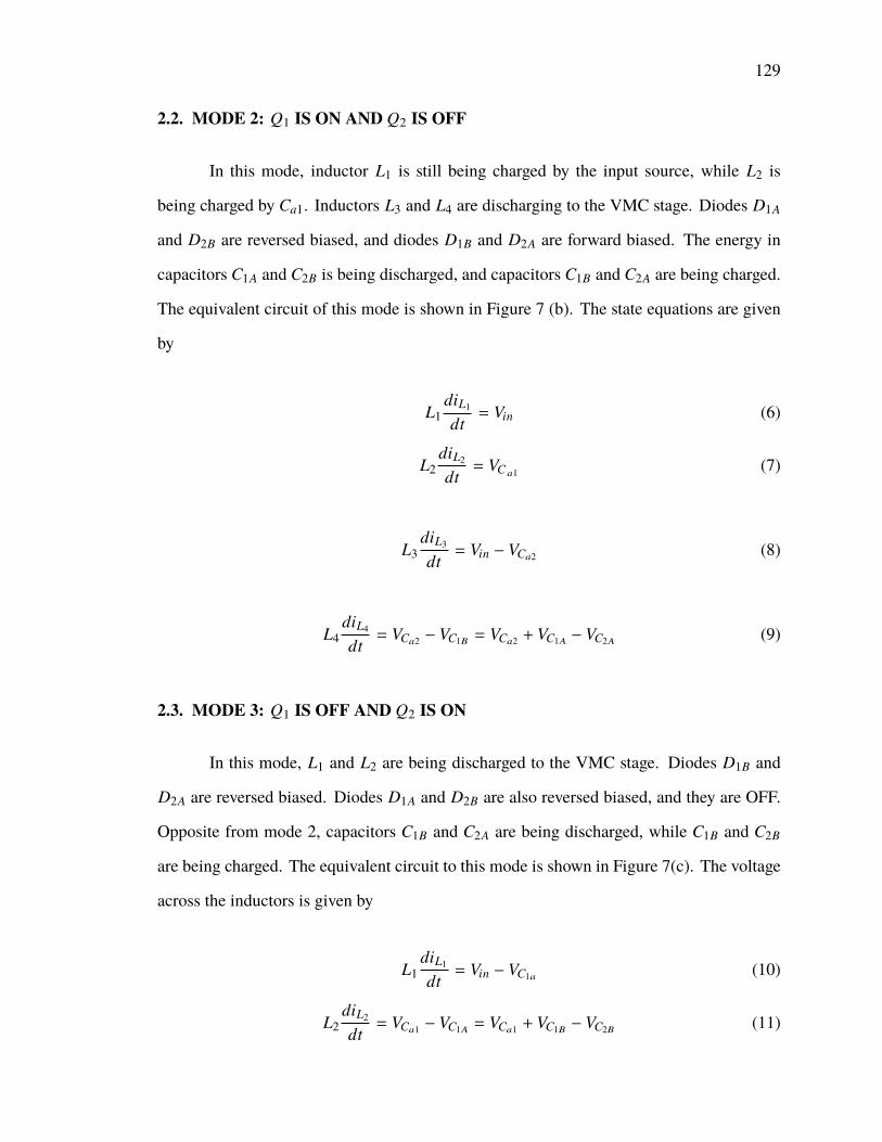
129
2.2. MODE 2: Q1 IS ON AND Q2 IS OFF
In this mode, inductor L1 is still being charged by the input source, while L2 is
being charged by Ca1. Inductors L3 and L4 are discharging to the VMC stage. Diodes D1A
and D2B are reversed biased, and diodes D1B and D2A are forward biased. The energy in
capacitors C1A and C2B is being discharged, and capacitors C1B and C2A are being charged.
The equivalent circuit of this mode is shown in Figure 7 (b). The state equations are given
by
L1diL1
dt= Vin (6)
L2diL2
dt= VC a1 (7)
L3diL3
dt= Vin − VCa2 (8)
L4diL4
dt= VCa2 − VC1B = VCa2 + VC1A − VC2A (9)
2.3. MODE 3: Q1 IS OFF AND Q2 IS ON
In this mode, L1 and L2 are being discharged to the VMC stage. Diodes D1B and
D2A are reversed biased. Diodes D1A and D2B are also reversed biased, and they are OFF.
Opposite from mode 2, capacitors C1B and C2A are being discharged, while C1B and C2B
are being charged. The equivalent circuit to this mode is shown in Figure 7(c). The voltage
across the inductors is given by
L1diL1
dt= Vin − VC1a (10)
L2diL2
dt= VCa1 − VC1A = VCa1 + VC1B − VC2B (11)

130
L3diL3
dt= Vin (12)
L4diL4
dt= VC a2 (13)
2.4. STEADY-STATE ANALYSIS AND STATIC VOLTAGE GAIN
By applying voltage-second balance to the inductors, the voltage across the capac-
itors and the output voltage, as well as the voltage gain of the converter, can be obtained.
The capacitor voltages are given by
VCa1 = VCa1 =Vin
1 − d(14)
VC1A = VC1B =Vin
(1 − d)2(15)
VC2A = VC2B =2Vin
(1 − d)2(16)
And the output voltage gain is given by
Vo =4Vin
(1 − d)2(17)
The output voltage gain of the proposed converter with k boost converter stages and
N VMC cells is given by
M =2N
(1 − d)k(18)
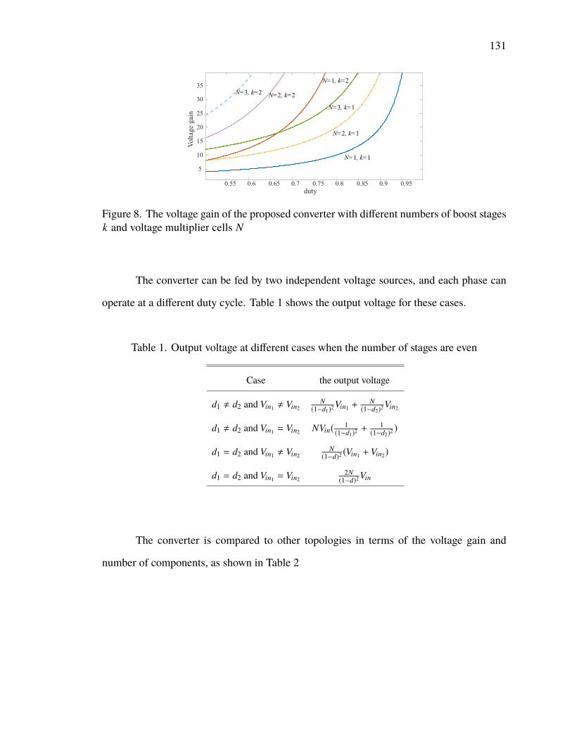
131
duty0.55 0.6 0.65 0.7 0.75 0.8 0.85 0.9 0.95
Volt
age
gai
n
5
10
15
20
25
30
35
N=1, k=1
N=1, k=2
N=2, k=1
N=2, k=2
N=3, k=1
N=3, k=2
Figure 8. The voltage gain of the proposed converter with different numbers of boost stagesk and voltage multiplier cells N
The converter can be fed by two independent voltage sources, and each phase can
operate at a different duty cycle. Table 1 shows the output voltage for these cases.
Table 1. Output voltage at different cases when the number of stages are even
Case the output voltage
d1 , d2 and Vin1 , Vin2N
(1−d1)2Vin1 +
N(1−d2)2
Vin2
d1 , d2 and Vin1 = Vin2 NVin(1
(1−d1)2+ 1(1−d2)2
)
d1 = d2 and Vin1 , Vin2N
(1−d)2 (Vin1 + Vin2)
d1 = d2 and Vin1 = Vin22N(1−d)2 Vin
The converter is compared to other topologies in terms of the voltage gain and
number of components, as shown in Table 2

132
Table 2. Comparison between different topologies
Topology Quadratic cascadedboost converter [34]
Cascaded three-levelboost converter (two stages) [35]
Interleaved boostwith the Dickson VMC with N = 5 [32]
Interleaved quadraticboost converter [36]
Proposed Converterwith N = 2, k = 2
Static voltage gain 1(1−d)2
1(1−d)2
61−D
1(1−D)2
4(1−D)2
Maximum stresson switches or diodes Vo
Vo
2Vo
N VoVo
2
Maximum voltageon capacitors Vo
Vo
2 Vo VoVo
2
Number ofcapacitors 2 4 6 3 6
Number ofdiodes 2 4 6 6 8
Number ofinductors 1 2 2 4 4
Number of floatingactive switches − 2 − − −
Number of groundedactive switches 2 2 2 2 2
3. COMPONENTS SELECTION AND EFFICIENCY ANALYSIS
3.1. ACTIVE SWITCHES
The voltage stress across the MOSFETs are given by
VQ1 = VQ2 = Vin1
(1 − d)2=
Vo
2N(19)
and the maximum current passing through the active switches is given by
IS1,pk =NVo
R3 − 2d
(1 − d)2−
Vin
2 fs
(1 − d
L1+
1L2−
d(1 − d)L4
)(20)
IS2,pk =NVo
R3 − 2d
(1 − d)2−
Vin
2 fs
(1 − d
L3+
1L4−
d(1 − d)L2
)(21)
The rms currents can be approximated using the following equation
IS1,rms = IS2,rms =NVo
R
√4
(1 − d)2+
1(1 − d)4
(22)
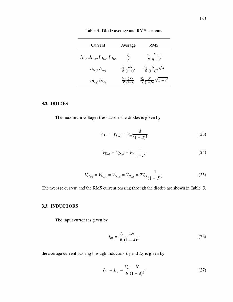
133
Table 3. Diode average and RMS currents
Current Average RMS
ID1A, ID1B, ID2A, ID2BVo
RVo
R
√1
1−d
IDa1, IDa3
Vo
RdN(1−d)2
Vo
RN
(1−d)2√
d
IDa2, IDa4
Vo
R(N)(1−d)
Vo
RN
(1−d)2√
1 − d
3.2. DIODES
The maximum voltage stress across the diodes is given by
VDa1 = VDa3 = Vind
(1 − d)2(23)
VDa2 = VDa4 = Vin1
1 − d(24)
VD1A = VD2A = VD1B = VD2B = 2Vin1
(1 − d)2(25)
The average current and the RMS current passing through the diodes are shown in Table. 3.
3.3. INDUCTORS
The input current is given by
Iin =Vo
R2N(1 − d)2
(26)
the average current passing through inductors L1 and L3 is given by
IL1 = IL3 =Vo
RN
(1 − d)2(27)
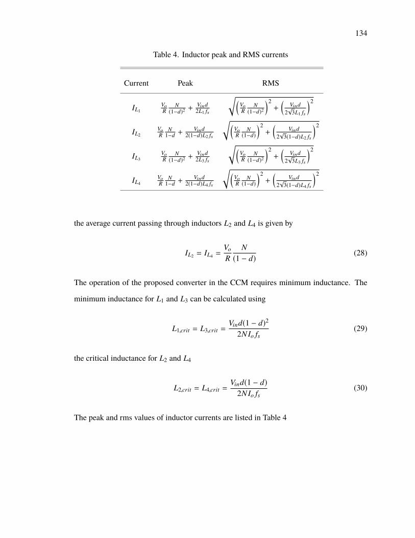
134
Table 4. Inductor peak and RMS currents
Current Peak RMS
IL1Vo
RN
(1−d)2 +Vind2L1 fs
√(Vo
RN
(1−d)2
)2+
(Vind
2√
3L1 fs
)2
IL2Vo
RN
1−d +Vind
2(1−d)L2 fs
√(Vo
RN(1−d)
)2+
(Vind
2√
3(1−d)L2 fs
)2
IL3Vo
RN
(1−d)2 +Vind2L3 fs
√(Vo
RN
(1−d)2
)2+
(Vind
2√
3L3 fs
)2
IL4Vo
RN
1−d +Vind
2(1−d)L4 fs
√(Vo
RN(1−d)
)2+
(Vind
2√
3(1−d)L4 fs
)2
the average current passing through inductors L2 and L4 is given by
IL2 = IL4 =Vo
RN
(1 − d)(28)
The operation of the proposed converter in the CCM requires minimum inductance. The
minimum inductance for L1 and L3 can be calculated using
L1,crit = L3,crit =Vind(1 − d)2
2NIo fs(29)
the critical inductance for L2 and L4
L2,crit = L4,crit =Vind(1 − d)
2NIo fs(30)
The peak and rms values of inductor currents are listed in Table 4
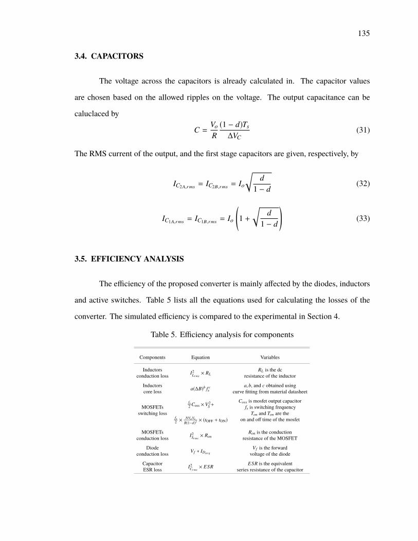
135
3.4. CAPACITORS
The voltage across the capacitors is already calculated in. The capacitor values
are chosen based on the allowed ripples on the voltage. The output capacitance can be
caluclaced by
C =Vo
R(1 − d)Ts
∆VC(31)
The RMS current of the output, and the first stage capacitors are given, respectively, by
IC2A,rms = IC2B,rms = Io
√d
1 − d(32)
IC1A,rms = IC1B,rms = Io
(1 +
√d
1 − d
)(33)
3.5. EFFICIENCY ANALYSIS
The efficiency of the proposed converter is mainly affected by the diodes, inductors
and active switches. Table 5 lists all the equations used for calculating the losses of the
converter. The simulated efficiency is compared to the experimental in Section 4.
Table 5. Efficiency analysis for components
Components Equation Variables
Inductorsconduction loss I2
Lrms× RL
RL is the dcresistance of the inductor
Inductorscore loss a(∆B)b f c
sa, b, and c obtained using
curve fitting from material datasheet
MOSFETsswitching loss
fs2 Coss × V2
S +
fs2 ×
NVoVs
R(1−d)2× (tOFF + tON)
Coss is mosfet output capacitorfs is switching frequency
Ton and Ton are theon and off time of the mosfet
MOSFETsconduction loss I2
Srms× Ron
Ron is the conductionresistance of the MOSFET
Diodeconduction loss Vf ∗ IDavg
Vf is the forwardvoltage of the diode
CapacitorESR loss I2
Crms× ESR
ESR is the equivalentseries resistance of the capacitor

136
Table 6. Component Listing for the Hardware Prototype
Item Designation Rating Part No.
Inductor L1 − L4 100 µH, DCR = 25 mΩ, 60B104C
Capacitor C1A,C2AC1BC2B
10 µF EXH2E106HRPT
Capacitor Ca1,Ca2 10 µF B32674D3106K
MOSFET Q1,Q2150 V,37 A
Rds(on) = 10.525 mΩ IPA105N15N3
Diode D1A,D2AD1B,D2B
250V,40AVF = 0.86 V, trr = 35 ns MBR40250G
4. EXPERIMENTAL IMPLEMENTATION AND RESULTS
An 80 W hardware prototype was implemented and tested in the laboratory to verify
the operation and the analysis of the converter. Figure 9 shows the hardware prototype,
which was implemented using the components listed in Table. 6. The N5700 was used to
supply power at 10 V to the prototype, and the output load was implemented using a mix of
ceramic resistors. The duty cycle was set to be around 0.6, and that made the output equal to
250 V . The measurements and waveforms were taken at 80 V . Figure 10 shows the voltage
waveforms across the switches. The active switches have a maximum voltage stress of 62 V .
The maximum voltage stress across the diodes in the interleaved single-switch multistage is
about 38 V for Da1 and Da3 and about 63 V for Da2 and Da4. The maximum voltage stress
across the VMC diodes is 125 V . The voltage across the capacitors, depicted in Figure 11,
is 25 V for C1 and C2, 63 V for C1A and C1B and 125 V for C2A and C2B. The output voltage
is about 250 V with ac components of less than 2%. Other waveforms such as the current of
the switches and passive components are shown in Figure 12 and Figure 13. The efficiency
of the converter was simulated and experimentally measured, as shown in Figure 14. As
mentioned before, the efficiency can be further increased by selecting efficient diodes with
low forward voltage for the interleaved boost stage or by replacing the diodes with efficient
ones or MOSFETs.
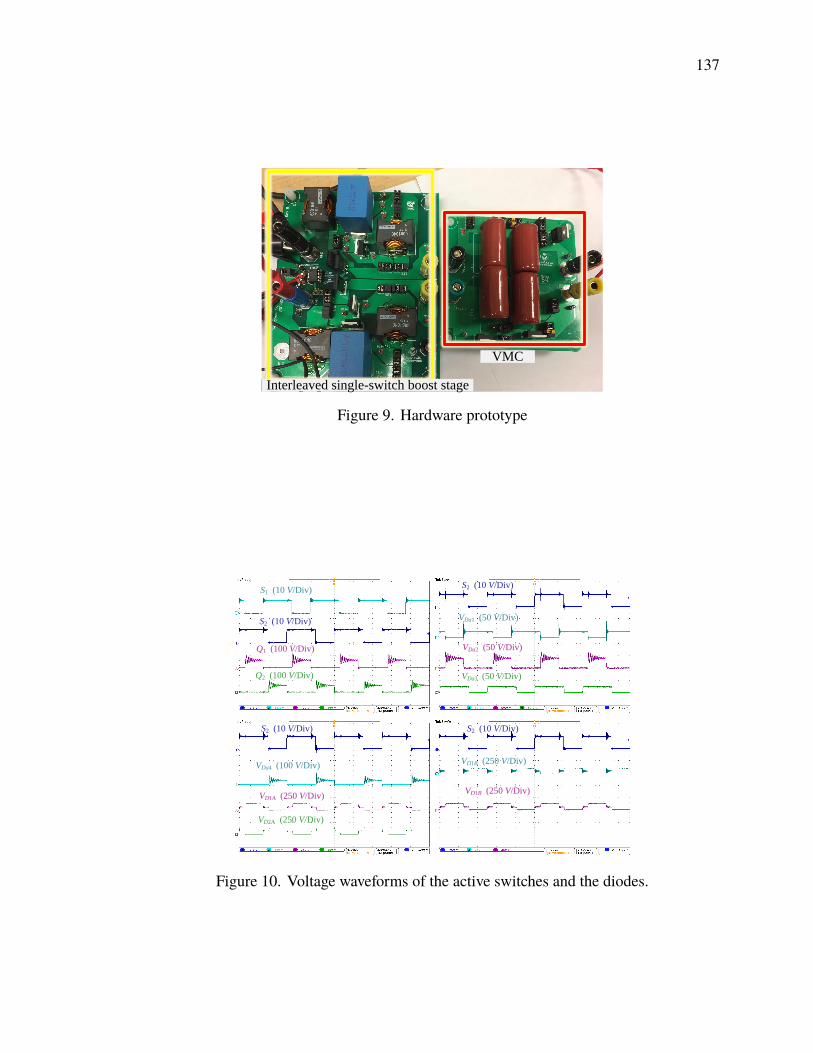
137
VMC
Interleaved single-switch boost stage
Figure 9. Hardware prototype
S2 (10 V/Div)
S2 (10 V/Div)
S1 (10 V/Div)
Q2 (100 V/Div)
Q1 (100 V/Div)
VDa1 (50 V/Div)
VDa3 (50 V/Div)
VDa2 (50 V/Div)
S2 (10 V/Div)
VDa4 (100 V/Div)
VD2A (250 V/Div)
VD1A (250 V/Div)
S2 (10 V/Div)
VD1B (250 V/Div)
VD1B (250 V/Div)
Figure 10. Voltage waveforms of the active switches and the diodes.

138
S2 (10 V/Div) S2 (10 V/Div)
S2 (10 V/Div)
VC1 (50 V/Div)
VC1A (50 V/Div)
VC2 (50 V/Div)
VC2A (100 V/Div)
VC1B (50 V/Div)
VC2B (100 V/Div)
VCo (250 V/Div)
ΔVCo (5 V/Div)
Figure 11. Voltage waveforms of the capacitors, the output load and the ac components ofthe output voltage.
Iin= 8.4 A (2 A/Div)
IL2=4.2 A (2 A/Div)IL1=4.2 A (2 A/Div)
IL3= 1.7 A (2 A/Div)
IQ1 (10 A/Div)
IL4=1.7 A (2 A/Div)
S2 (10 V/Div) S2 (10 V/Div)
S2 (10 V/Div) S2 (10 V/Div)
IQ2 (10 A/Div)
IDa1 (5 A/Div)
IDa3 (5 A/Div)
IDa2 (5 A/Div)
IDa4 (5 A/Div)
ID1A (2 A/Div)
Figure 12. Current passing through the active switches, inductors and diodes D11-D23
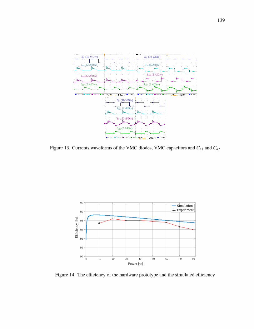
139
ID2A (2 A/Div)
ID1B (2 A/Div)
ID2B (2 A/Div)
ICa1 (5 A/Div)
ICa2 (5 A/Div)
IC1A (2 A/Div)
IC2A (2 A/Div)
IC1B (2 A/Div)
IC2B (2 A/Div)
S2 (10 V/Div)
S2 (10 V/Div) S2 (10 V/Div)
Figure 13. Currents waveforms of the VMC diodes, VMC capacitors and Ca1 and Ca2
0 10 20 30 40 50 60 70 8090
91
92
93
94
95
96Simulation
Experiment
Eff
icie
ncy
[%
]
Power [w]
Figure 14. The efficiency of the hardware prototype and the simulated efficiency

140
5. CONCLUSIONS
This paper presents a non-isolated interleavedmultistage boost converter with VMC.
The converter has a high voltage and low voltage stresses across the components. Converting
a 10V to a 250 V can be achieved by the quadratic boost stage and a 2-cell VMC when
operating at a 0.6 duty ratio. The converter is capable of converting power from a single
source or two independent sources. The input is shared among the two phases equally, and
since the converter operates at 0.6 the current ripple cancellation is higher than the other
interleaved boost converters. The analysis of this converter was explained and validated by
simulation and experimental prototype. The converter is very suitable for integrating PV
panels to higher voltage DC buses.
REFERENCES
[1] R. Wai, C. Lin, R. Duan, and Y. Chang, “High-efficiency dc-dc converter with highvoltage gain and reduced switch stress,” IEEE Transactions on Industrial Electronics,vol. 54, no. 1, pp. 354–364, Feb 2007.
[2] O. Abutbul, A. Gherlitz, Y. Berkovich, and A. Ioinovici, “Step-up switching-modeconverter with high voltage gain using a switched-capacitor circuit,” IEEE Transac-tions on Circuits and Systems I: Fundamental Theory and Applications, vol. 50, no. 8,pp. 1098–1102, Aug 2003.
[3] G. A. Henn, R. Silva, P. P. Praca, L. Barreto, and D. S. Oliveira Jr, “Interleaved-boostconverter with high voltage gain,” IEEE transactions on power electronics, vol. 25,no. 11, pp. 2753–2761, 2010.
[4] M. Lakshmi and S. Hemamalini, “Nonisolated high gain dc–dc converter for dcmicrogrids,” IEEE Transactions on Industrial Electronics, vol. 65, no. 2, pp. 1205–1212, Feb 2018.
[5] J. M. Carrasco, L. G. Franquelo, J. T. Bialasiewicz, E. Galvan, R. C. PortilloGuisado,M. A. M. Prats, J. I. Leon, and N. Moreno-Alfonso, “Power-electronic systems forthe grid integration of renewable energy sources: A survey,” IEEE Transactions onIndustrial Electronics, vol. 53, no. 4, pp. 1002–1016, June 2006.
[6] B. Nordman and K. Christensen, “Dc local power distribution: Technology, deploy-ment, and pathways to success,” IEEE Electrification Magazine, vol. 4, no. 2, pp.29–36, June 2016.
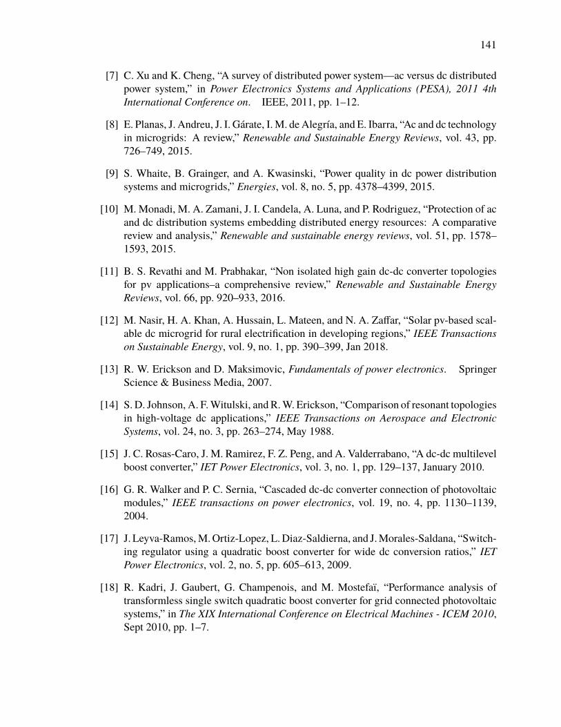
141
[7] C. Xu and K. Cheng, “A survey of distributed power system—ac versus dc distributedpower system,” in Power Electronics Systems and Applications (PESA), 2011 4thInternational Conference on. IEEE, 2011, pp. 1–12.
[8] E. Planas, J. Andreu, J. I. Gárate, I.M. deAlegría, and E. Ibarra, “Ac and dc technologyin microgrids: A review,” Renewable and Sustainable Energy Reviews, vol. 43, pp.726–749, 2015.
[9] S. Whaite, B. Grainger, and A. Kwasinski, “Power quality in dc power distributionsystems and microgrids,” Energies, vol. 8, no. 5, pp. 4378–4399, 2015.
[10] M. Monadi, M. A. Zamani, J. I. Candela, A. Luna, and P. Rodriguez, “Protection of acand dc distribution systems embedding distributed energy resources: A comparativereview and analysis,” Renewable and sustainable energy reviews, vol. 51, pp. 1578–1593, 2015.
[11] B. S. Revathi and M. Prabhakar, “Non isolated high gain dc-dc converter topologiesfor pv applications–a comprehensive review,” Renewable and Sustainable EnergyReviews, vol. 66, pp. 920–933, 2016.
[12] M. Nasir, H. A. Khan, A. Hussain, L. Mateen, and N. A. Zaffar, “Solar pv-based scal-able dc microgrid for rural electrification in developing regions,” IEEE Transactionson Sustainable Energy, vol. 9, no. 1, pp. 390–399, Jan 2018.
[13] R. W. Erickson and D. Maksimovic, Fundamentals of power electronics. SpringerScience & Business Media, 2007.
[14] S. D. Johnson, A. F.Witulski, and R.W. Erickson, “Comparison of resonant topologiesin high-voltage dc applications,” IEEE Transactions on Aerospace and ElectronicSystems, vol. 24, no. 3, pp. 263–274, May 1988.
[15] J. C. Rosas-Caro, J. M. Ramirez, F. Z. Peng, and A. Valderrabano, “A dc-dc multilevelboost converter,” IET Power Electronics, vol. 3, no. 1, pp. 129–137, January 2010.
[16] G. R. Walker and P. C. Sernia, “Cascaded dc-dc converter connection of photovoltaicmodules,” IEEE transactions on power electronics, vol. 19, no. 4, pp. 1130–1139,2004.
[17] J. Leyva-Ramos,M.Ortiz-Lopez, L.Diaz-Saldierna, and J.Morales-Saldana, “Switch-ing regulator using a quadratic boost converter for wide dc conversion ratios,” IETPower Electronics, vol. 2, no. 5, pp. 605–613, 2009.
[18] R. Kadri, J. Gaubert, G. Champenois, and M. Mostefaï, “Performance analysis oftransformless single switch quadratic boost converter for grid connected photovoltaicsystems,” in The XIX International Conference on Electrical Machines - ICEM 2010,Sept 2010, pp. 1–7.
142
[19] E. H. Ismail, M. A. Al-Saffar, A. J. Sabzali, and A. A. Fardoun, “A family of single-switch pwm converters with high step-up conversion ratio,” IEEE Transactions onCircuits and Systems I: Regular Papers, vol. 55, no. 4, pp. 1159–1171, May 2008.
[20] F. L. Luo and H. Ye, Advanced dc/dc converters. crc Press, 2016.
[21] J.-M. Kwon, B.-H. Kwon, and K.-H. Nam, “Three-phase photovoltaic system withthree-level boosting mppt control,” IEEE Transactions on Power Electronics, vol. 23,no. 5, pp. 2319–2327, 2008.
[22] V. Yaramasu, B. Wu, S. Alepuz, and S. Kouro, “Predictive control for low-voltageride-through enhancement of three-level-boost and npc-converter-based pmsg windturbine,” IEEE Transactions on Industrial Electronics, vol. 61, no. 12, pp. 6832–6843,2014.
[23] A. Chub, D. Vinnikov, F. Blaabjerg, and F. Z. Peng, “A review of galvanically isolatedimpedance-source dc-dc converters,” IEEETransactions onPowerElectronics, vol. 31,no. 4, pp. 2808–2828, April 2016.
[24] I. Barbi and R. Gules, “Isolated dc-dc converters with high-output voltage for twtatelecommunication satellite applications,” IEEE Transactions on Power Electronics,vol. 18, no. 4, pp. 975–984, 2003.
[25] M.-K. Nguyen, Y.-C. Lim, J.-H. Choi, and G.-B. Cho, “Isolated high step-up dc-dcconverter based on quasi-switched-boost network.” IEEETrans. Industrial Electronics,vol. 63, no. 12, pp. 7553–7562, 2016.
[26] J. Duarte, L. Lima, L. Oliveira, M.Mezaroba, L.Michels, and C. Rech, “Modeling anddigital control of a single-stage step-up/down isolated pfc rectifier,” IEEE Transactionson Industrial Informatics, vol. 9, no. 2, pp. 1017–1028, 2013.
[27] F. Evran and M. T. Aydemir, “Isolated high step-up dc–dc converter with low voltagestress,” IEEE Transactions on Power Electronics, vol. 29, no. 7, pp. 3591–3603, 2014.
[28] F. L. Tofoli, D. d. C. Pereira, W. J. de Paula, and D. d. S. Oliveira Júnior, “Survey onnon-isolated high-voltage step-up dc-dc topologies based on the boost converter,” IETPower Electronics, vol. 8, no. 10, pp. 2044–2057, 2015.
[29] M. Forouzesh, Y. P. Siwakoti, S. A. Gorji, F. Blaabjerg, and B. Lehman, “Step-updc–dc converters: a comprehensive review of voltage-boosting techniques, topologies,and applications,” IEEE Transactions on Power Electronics, vol. 32, no. 12, pp. 9143–9178, 2017.
[30] W. Li and X. He, “Review of nonisolated high-step-up dc/dc converters in photovoltaicgrid-connected applications,” IEEE Transactions on Industrial Electronics, vol. 58,no. 4, pp. 1239–1250, April 2011.
143
[31] A. Alzahrani, P. Shamsi, and M. Ferdowsi, “Boost converter with bipolar dicksonvoltage multiplier cells,” in Renewable Energy Research and Applications (ICRERA),2017 IEEE 6th International Conference on. IEEE, 2017, pp. 228–233.
[32] V.A.K. Prabhala, P. Fajri, V. S. P. Gouribhatla, B. P. Baddipadiga, andM. Ferdowsi, “Adc–dc converter with high voltage gain and two input boost stages,” IEEE Transactionson Power Electronics, vol. 31, no. 6, pp. 4206–4215, June 2016.
[33] M. Fu, C. Zhao, J. Song, and C. Ma, “A low-cost voltage equalizer based on wirelesspower transfer and a voltage multiplier,” IEEE Transactions on Industrial Electronics,vol. 65, no. 7, pp. 5487–5496, July 2018.
[34] O. López-Santos, L. Martínez-Salamero, G. García, H. Valderrama-Blavi, andT. Sierra-Polanco, “Comparison of quadratic boost topologies operating under sliding-mode control,” in Power Electronics Conference (COBEP), 2013, pp. 66–71.
[35] W. Li, X. Lv, Y. Deng, J. Liu, and X. He, “A review of non-isolated high step-up dc/dcconverters in renewable energy applications,” in 2009 Twenty-Fourth Annual IEEEApplied Power Electronics Conference and Exposition, Feb 2009, pp. 364–369.
[36] S. Balci, N. Altin, H. Komurcugil, and I. Sefa, “Performance analysis of interleavedquadratic boost converter with coupled inductor for fuel cell applications,” in IECON2016 - 42nd Annual Conference of the IEEE Industrial Electronics Society, Oct 2016,pp. 3541–3546.
144
SECTION
2. SUMMARY AND CONCLUSIONS
This dissertation has presented several advanced high-voltage-gain dc-dc step-up
topologies suitable for renewable energy sources integration to a high voltage dc distribution
bus. First, a family of interleaved boost converters with VMCs was presented. The family
consists of two stages: an interleaved boost stage and a VMC stage, which mainly consist
of diodes and capacitors and are expendable. The output of the VMC can be filtered
by an output diode and output capacitors or by an LC filter. Many group combinations
are presented and compared in terms of the voltage gain, output-input connection, input
current sharing among inductors, and the number of capacitors and diodes per stage. An
example converter to efficiently convert a 20 V to a 400 V was designed and verified by
simulation and experimental results. The second paper has presented a novel VMC and
connected it to an interleaved boost converter with no need of an output diode or LC filter.
Therefore, the output is fed by two capacitors and the voltage is rectified at each VMC
stage. The proposed converter features a have high voltage gain, equal current sharing,
low voltage stress across components, and better ripple cancellation across capacitors. The
proposed converter was analyzed, and the design process was explained. A 200 W hardware
prototype was implemented to convert 20 V input to 400 V output. The converter has a peak
efficiency of 96% andmaximumvoltage stress across components less than 135 V . The third
paper presents a hybrid fly-multilevel boost converter. The converter utilizes the multilevel
structure to increase the effective frequency across the magnetic device, which is a flyback
transformer. The proposed hybrid multilevel boost converters have most required features
for renewable energy applications, such as low stress across components, high voltage
gain, drawing continuous current, and small magnetic elements. The converter modes
145
of operation and steady-state analysis are presented and verified by simulation. Further
verification was ensured by implementing a hardware prototype of an example converter
to convert 20 V to 200 V for 100 W output load power. Paper four presents an interleaved
multistage boost converter with VMC. In this topology, each phase of the interleaved stage
can have the same or a different number of boost stages, and all phases share the VMC. The
theory of operation, the steady-state analysis is presented for example converter, which has
an interleaved quadratic boost stage with two-stage VMC. The converter was analyzed and
verified by simulation results. A hardware prototype was implemented to convert 10 V to
250 V and 200 W to prove the operation and further verify the simulation results. Future
work includes experimentation of large PV side surfaced and more panels to demonstrate
the benefit of the proposed structures over the flat regular solar PV panels and closed-
loop analysis and control of the proposed converters. Different control schemes have to
be further studied, and further details about MPPT extraction algorithms under different
weather conditions are required to reveal the operation of the proposed converters further.
146
REFERENCES
[1] B. P. Baddipadiga and M. Ferdowsi. A high-voltage-gain dc-dc converterbased on modified dickson charge pump voltage multiplier. IEEE Transactionson Power Electronics, 32(10):7707–7715, Oct 2017. ISSN 0885-8993. doi:10.1109/TPEL.2016.2594016.
[2] Mojtaba Forouzesh, Yam P Siwakoti, Saman A Gorji, Frede Blaabjerg, and BradLehman. Step-up dc–dc converters: a comprehensive review of voltage-boostingtechniques, topologies, and applications. IEEE Transactions on Power Electronics,32(12):9143–9178, 2017.
[3] Johann W. Kolar. Future challenges for research and teaching in power electronics,2014. International Conference on Optimization of Electrical and Electronic Equip-ment, OPTIM 2014; Conference Location: Brasov, Rumania; Conference Date: May22-24, 2014; Conference lecture on 23 May 2014.
[4] R. Hans, A. Manfred, P. Janina, and S. Alexander. Improved characterization of themagnetic properties of hexagonally packed wires. In Proceedings of the 2011 14thEuropean Conference on Power Electronics and Applications, pages 1–9, Aug 2011.
[5] J. M. Carrasco, L. G. Franquelo, J. T. Bialasiewicz, E. Galvan, R. C. PortilloGuisado,M. A. M. Prats, J. I. Leon, and N. Moreno-Alfonso. Power-electronic systems forthe grid integration of renewable energy sources: A survey. IEEE Transactionson Industrial Electronics, 53(4):1002–1016, June 2006. ISSN 0278-0046. doi:10.1109/TIE.2006.878356.
[6] Bin Lu, Edwin L Piner, and Tomás Palacios. Schottky-drain technology for algan/ganhigh-electron mobility transistors. IEEE Electron Device Letters, 31(4):302–304,2010.
[7] Robert W Erickson and Dragan Maksimovic. Fundamentals of power electronics.Springer Science & Business Media, 2007.
[8] Marian K Kazimierczuk. Pulse-width modulated DC-DC power converters. JohnWiley & Sons, 2015.
[9] F. L. Tofoli, D. d. C. Pereira, W. Josias de Paula, and D. d. S. Oliveira Júnior.Survey on non-isolated high-voltage step-up dc-dc topologies based on the boostconverter. IET Power Electronics, 8(10):2044–2057, 2015. ISSN 1755-4535. doi:10.1049/iet-pel.2014.0605.
[10] L. Huber and M. M. Jovanovic. A design approach for server power supplies fornetworking applications. In APEC 2000. Fifteenth Annual IEEE Applied Power Elec-tronics Conference and Exposition (Cat. No.00CH37058), volume 2, pages 1163–1169 vol.2, Feb 2000. doi: 10.1109/APEC.2000.822834.
147
[11] Tsai-Fu Wu and Te-Hung Yu. Unified approach to developing single-stage powerconverters. IEEE Transactions on Aerospace and Electronic Systems, 34(1):211–223,Jan 1998. ISSN 0018-9251. doi: 10.1109/7.640279.
[12] J. Leyva-Ramos, M. G. Ortiz-Lopez, L. H. Diaz-Saldierna, and J. A. Morales-Saldana. Switching regulator using a quadratic boost converter forwide dc conversionratios. IET Power Electronics, 2(5):605–613, Sept 2009. ISSN 1755-4535. doi:10.1049/iet-pel.2008.0169.
[13] Fang Lin Luo and Hong Ye. Advanced dc/dc converters. crc Press, 2016.
[14] Fang Lin Luo and Hong Ye. Positive output cascade boost converters. IEEProceedings-Electric Power Applications, 151(5):590–606, 2004.
[15] M. G. Ortiz-Lopez, J. Leyva-Ramos, E. E. Carbajal-Gutierrez, and J. A. Morales-Saldana. Modelling and analysis of switch-mode cascade converters with a singleactive switch. IET Power Electronics, 1(4):478–487, December 2008. ISSN 1755-4535. doi: 10.1049/iet-pel:20070379.
[16] J-Y Lee and S-N Hwang. Non-isolated high-gain boost converter using voltage-stacking cell. Electronics Letters, 44(10):644–646, 2008.
[17] K. B. Park, G. W. Moon, and M. J. Youn. Nonisolated high step-up stacked converterbased on boost-integrated isolated converter. IEEE Transactions on Power Electron-ics, 26(2):577–587, Feb 2011. ISSN 0885-8993. doi: 10.1109/TPEL.2010.2066578.
[18] M. Tanca V. and I. Barbi. Nonisolated high step-up stacked dc-dc converter basedon boost converter elements for high power application. In 2011 IEEE Interna-tional Symposium of Circuits and Systems (ISCAS), pages 249–252, May 2011. doi:10.1109/ISCAS.2011.5937548.
[19] S. K. Changchien, T. J. Liang, J. F. Chen, and L. S. Yang. Novel high step-up dc-dc converter for fuel cell energy conversion system. IEEE Transactionson Industrial Electronics, 57(6):2007–2017, June 2010. ISSN 0278-0046. doi:10.1109/TIE.2009.2026364.
[20] Jesus Valdez-Resendiz, Julio Rosas-caro, Jonathan C Mayo-Maldonado, and Ar-mandoLlamas-Terres. Quadratic boost converter based on stackable switching stages.IET Power Electronics, 2018.
[21] M. T. Zhang, Yimin Jiang, F. C. Lee, and M. M. Jovanovic. Single-phase three-levelboost power factor correction converter. In Applied Power Electronics Conferenceand Exposition, 1995. APEC ’95. Conference Proceedings 1995., Tenth Annual,number 0, pages 434–439 vol.1, Mar 1995. doi: 10.1109/APEC.1995.468984.
[22] Jung-Min Kwon, Bong-Hwan Kwon, and Kwang-Hee Nam. Three-phase photo-voltaic system with three-level boosting mppt control. IEEE Transactions on PowerElectronics, 23(5):2319–2327, 2008.

148
[23] Ahmed Shahin, Melika Hinaje, Jean-Philippe Martin, Serge Pierfederici, StéphaneRaël, andBernardDavat. High voltage ratio dc–dc converter for fuel-cell applications.IEEE Transactions on Industrial Electronics, 57(12):3944–3955, 2010.
[24] João Paulo M Figueiredo, Fernando L Tofoli, and Bruno Leonardo A Silva. A reviewof single-phase pfc topologies based on the boost converter. In Industry Applications(INDUSCON), 2010 9th IEEE/IAS International Conference on, pages 1–6. IEEE,2010.
[25] VenkataYaramasu andBinWu. Predictive control of a three-level boost converter andan npc inverter for high-power pmsg-based medium voltage wind energy conversionsystems. IEEE Trans. Power Electron, 29(10):5308–5322, 2014.
[26] Ned Mohan and Tore M Undeland. Power electronics: converters, applications, anddesign. John Wiley & Sons, 2007.
[27] R. P. Severus. A new current-fed converter topology. In 1979 IEEEPower Electronics Specialists Conference, pages 277–283, June 1979. doi:10.1109/PESC.1979.7081036.
[28] L Wuidart. Topologies for switched mode power supplies. Application Note AN,513:0393, 1999.
[29] Michael Douglas Seeman. A design methodology for switched-capacitor DC-DCconverters. University of California, Berkeley, 2009.
[30] M. D. Seeman and S. R. Sanders. Analysis and optimization of switched-capacitordc-dc converters. IEEE Transactions on Power Electronics, 23(2):841–851, March2008. ISSN 0885-8993. doi: 10.1109/TPEL.2007.915182.
[31] G. Palumbo and D. Pappalardo. Charge pump circuits: An overview on designstrategies and topologies. IEEE Circuits and Systems Magazine, 10(1):31–45, First2010. ISSN 1531-636X. doi: 10.1109/MCAS.2009.935695.
[32] M. S. Makowski. Realizability conditions and bounds on synthesis of switched-capacitor dc-dc voltage multiplier circuits. IEEE Transactions on Circuits and Sys-tems I: Fundamental Theory and Applications, 44(8):684–691, Aug 1997. ISSN1057-7122. doi: 10.1109/81.611263.
[33] J. W. Kimball. Performance analysis of generalized algebraic switched capacitorconverters. In 2013 IEEE Energy Conversion Congress and Exposition, pages 1808–1813, Sept 2013. doi: 10.1109/ECCE.2013.6646927.
[34] A.Kushnerov and S. Ben-yaakov. Unified algebraic synthesis of generalised fibonacciswitched capacitor converters. IET Power Electronics, 7(3):540–544, March 2014.ISSN 1755-4535. doi: 10.1049/iet-pel.2013.0197.

149
[35] L. Balogh and R. Redl. Power-factor correction with interleaved boost convert-ers in continuous-inductor-current mode. In Proceedings Eighth Annual AppliedPower Electronics Conference and Exposition,, pages 168–174, March 1993. doi:10.1109/APEC.1993.290634.
[36] Dean RGarth, WJMuldoon, GCBenson, and ENCostague. Multi-phase, 2-kilowatt,high-voltage, regulated power supply. In Power Electronics Specialists Conference,1971 IEEE, pages 110–116. IEEE, 1971.
[37] B. A.Miwa, D.M. Otten, andM. E. Schlecht. High efficiency power factor correctionusing interleaving techniques. In [Proceedings] APEC ’92 Seventh Annual AppliedPower Electronics Conference and Exposition, pages 557–568, Feb 1992. doi:10.1109/APEC.1992.228361.
[38] R. Giral, L. Martinez-Salamero, and S. Singer. Interleaved converters operationbased on cmc. IEEE Transactions on Power Electronics, 14(4):643–652, July 1999.ISSN 0885-8993. doi: 10.1109/63.774201.
[39] Michael O’Loughlin. An interleaving pfc pre-regulator for high-power converters.Texas Instruments, pages 1–14, 2006.
[40] R. Gules, L. L. Pfitscher, and L. C. Franco. An interleaved boost dc-dc converterwith large conversion ratio. In 2003 IEEE International Symposium on IndustrialElectronics ( Cat. No.03TH8692), volume 1, pages 411–416 vol. 1, June 2003. doi:10.1109/ISIE.2003.1267284.
[41] Wuhua Li, Yi Zhao, Yan Deng, and Xiangning He. Interleaved converter with voltagemultiplier cell for high step-up and high-efficiency conversion. IEEE Transactionson Power Electronics, 25(9):2397–2408, 2010.
[42] M. M. Jovanovic. A technique for reducing rectifier reverse-recovery-related lossesin high-power boost converters. IEEE Transactions on Power Electronics, 13(5):932–941, Sep 1998. ISSN 0885-8993. doi: 10.1109/63.712314.
[43] Remus Teodorescu, Marco Liserre, and Pedro Rodriguez. Grid converters for pho-tovoltaic and wind power systems, volume 29. John Wiley & Sons, 2011.
[44] F. Blaabjerg, Y. Yang, and K. Ma. Power electronics - key technology for re-newable energy systems - status and future. In 2013 3rd International Conferenceon Electric Power and Energy Conversion Systems, pages 1–6, Oct 2013. doi:10.1109/EPECS.2013.6712980.
[45] Johann W Kolar, Jürgen Biela, Stefan Waffler, Thomas Friedli, and Uwe Badstübner.Performance trends and limitations of power electronic systems. In Integrated PowerElectronics Systems (CIPS), 2010 6th International Conference on, pages 1–20.IEEE, 2010.
[46] Jacobus Daniel van Wyk and Fred C Lee. On a future for power electronics. IEEEJournal of Emerging and Selected Topics in Power Electronics, 1(2):59–72, 2013.
150
[47] V. A. K. Prabhala, B. P. Baddipadiga, and M. Ferdowsi. Dc distribution sys-tems; an overview. In 2014 International Conference on Renewable Energy Re-search and Application (ICRERA), pages 307–312, Oct 2014. doi: 10.1109/ICR-ERA.2014.7016575.
[48] A. Pratt, P. Kumar, and T. V. Aldridge. Evaluation of 400v dc distribution intelco and data centers to improve energy efficiency. In INTELEC 07 - 29th Inter-national Telecommunications Energy Conference, pages 32–39, Sept 2007. doi:10.1109/INTLEC.2007.4448733.
[49] P. T. Krein. Data center challenges and their power electronics. CPSS Transactionson Power Electronics and Applications, 2(1):39–46, 2017. ISSN 2475-742X. doi:10.24295/CPSSTPEA.2017.00005.
[50] D. J. Hammerstrom. Ac versus dc distribution systemsdid we get it right? In 2007IEEE Power Engineering Society General Meeting, pages 1–5, June 2007. doi:10.1109/PES.2007.386130.
[51] A. Mohamed and O. Mohammed. Connectivity of dc microgrids involving sustain-able energy sources. In 2011 IEEE Industry Applications Society Annual Meeting,pages 1–8, Oct 2011. doi: 10.1109/IAS.2011.6074338.
[52] Venkata Anand Kishore Prabhala, Poria Fajri, Venkat Sai Prasad Gouribhatla,Bhanu Prashant Baddipadiga, and Mehdi Ferdowsi. A dc–dc converter with highvoltage gain and two input boost stages. IEEE Transactions on Power Electronics,31(6):4206–4215, 2016.
[53] Rong-Jong Wai, Chung-You Lin, Rou-Yong Duan, and Yung-Ruei Chang. High-efficiency dc-dc converter with high voltage gain and reduced switch stress. IEEETransactions on Industrial Electronics, 54(1):354–364, 2007.
[54] Lung-Sheng Yang, Tsorng-Juu Liang, and Jiann-Fuh Chen. Transformerless dc–dc converters with high step-up voltage gain. IEEE Transactions on IndustrialElectronics, 56(8):3144–3152, 2009.
[55] Qun Zhao and Fred C Lee. High-efficiency, high step-up dc-dc converters. IEEETransactions on Power Electronics, 18(1):65–73, 2003.
[56] Shih-Ming Chen, Tsorng-Juu Liang, Lung-Sheng Yang, and Jiann-Fuh Chen. A cas-caded high step-up dc–dc converter with single switch for microsource applications.IEEE Transactions on Power Electronics, 26(4):1146–1153, 2011.
[57] Nicholas Denniston, Ahmed M Massoud, Shehab Ahmed, and Prasad N Enjeti.Multiple-module high-gain high-voltage dc–dc transformers for offshorewind energysystems. IEEE Transactions on Industrial Electronics, 58(5):1877–1886, 2011.
[58] Zhigang Liang, Rong Guo, Jun Li, and Alex Q Huang. A high-efficiency pv module-integrated dc/dc converter for pv energy harvest in freedm systems. IEEE Transac-tions on Power Electronics, 26(3):897–909, 2011.

151
[59] Boris Axelrod, Yefim Berkovich, and Adrian Ioinovici. Transformerless dc-dc con-verters with a very high dc line-to-load voltage ratio. In Circuits and Systems, 2003.ISCAS’03. Proceedings of the 2003 International Symposium on, volume 3, pagesIII–III. IEEE, 2003.
[60] Suman Dwari and Leila Parsa. An efficient high-step-up interleaved dc–dc converterwith a common active clamp. IEEE Transactions on Power Electronics, 26(1):66–78,2011.
[61] Tsai-Fu Wu, Yung-Chu Chen, Jeng-Gung Yang, and Chia-Ling Kuo. Isolated bidi-rectional full-bridge dc–dc converter with a flyback snubber. IEEE Transactions onPower Electronics, 25(7):1915–1922, 2010.
[62] Felinto SF Silva, Antônio AA Freitas, Sérgio Daher, Saulo C Ximenes, Sarah KASousa, MS Edilson, Fernando LM Antunes, and Cícero MT Cruz. High gain dc-dcboost converter with a coupling inductor. In Power Electronics Conference, 2009.COBEP’09. Brazilian, pages 486–492. IEEE, 2009.
[63] Venkata Yaramasu and Bin Wu. Three-level boost converter based medium voltagemegawatt pmsg wind energy conversion systems. In Energy Conversion Congressand Exposition (ECCE), 2011 IEEE, pages 561–567. IEEE, 2011.
[64] Robert W Erickson and Dragan Maksimovic. Fundamentals of power electronics.Springer Science & Business Media, 2007.
[65] F. L. Tofoli, D. de Souza Oliveira, R. P. Torrico-Bascopé, and Y. J. A. Alcazar.Novel nonisolated high-voltage gain dc-dc converters based on 3ssc and vmc. IEEETransactions on Power Electronics, 27(9):3897–3907, Sept 2012. ISSN 0885-8993.doi: 10.1109/TPEL.2012.2190943.
[66] F. L. Tofoli, D. d. C. Pereira, W. Josias de Paula, and D. d. S. Oliveira Júnior.Survey on non-isolated high-voltage step-up dc-dc topologies based on the boostconverter. IET Power Electronics, 8(10):2044–2057, 2015. ISSN 1755-4535. doi:10.1049/iet-pel.2014.0605.
[67] R. Haroun, A. E. Aroudi, A. Cid-Pastor, G. Garcia, C. Olalla, and L. Martínez-Salamero. Impedance matching in photovoltaic systems using cascaded boost con-verters and sliding-mode control. IEEE Transactions on Power Electronics, 30(6):3185–3199, June 2015. ISSN 0885-8993. doi: 10.1109/TPEL.2014.2339134.
[68] M. Veerachary and S. B. Sudhakar. Stability analysis of cascaded dc-dc powerelectronic system. In 2007 7th International Conference on Power Electronics andDrive Systems, pages 1422–1426, Nov 2007. doi: 10.1109/PEDS.2007.4487890.
[69] M. Forouzesh, Y. P. Siwakoti, S. A. Gorji, F. Blaabjerg, and B. Lehman. Step-up dc-dc converters: A comprehensive review of voltage-boosting techniques, topologies,and applications. IEEE Transactions on Power Electronics, 32(12):9143–9178, Dec2017. ISSN 0885-8993. doi: 10.1109/TPEL.2017.2652318.
152
[70] B. P. R. Baddipadiga, V. A. Prabhala, andM. Ferdowsi. A family of high-voltage-gaindc-dc converters based on a generalized structure. IEEE Transactions on Power Elec-tronics, PP(99):1–1, 2017. ISSN 0885-8993. doi: 10.1109/TPEL.2017.2777451.
[71] R. Gules, L. L. Pfitscher, and L. C. Franco. An interleaved boost dc-dc converterwith large conversion ratio. In 2003 IEEE International Symposium on IndustrialElectronics ( Cat. No.03TH8692), volume 1, pages 411–416 vol. 1, June 2003. doi:10.1109/ISIE.2003.1267284.
[72] Ching-Ming Lai, Yuan-Chih Lin, and Dasheng Lee. Study and implementation ofa two-phase interleaved bidirectional dc/dc converter for vehicle and dc-microgridsystems. Energies, 8(9):9969–9991, 2015.
[73] M. Prudente, L. L. Pfitscher, G. Emmendoerfer, E. F. Romaneli, and R. Gules.Voltage multiplier cells applied to non-isolated dc–dc converters. IEEE Transac-tions on Power Electronics, 23(2):871–887, March 2008. ISSN 0885-8993. doi:10.1109/TPEL.2007.915762.
[74] PyosooKim, Sanghyuk Lee, Junsung Park, and SewanChoi. High step-up interleavedboost converters using voltage multiplier cells. In Power Electronics and ECCE Asia(ICPE and ECCE), 2011 IEEE 8th International Conference on, pages 2844–2851.IEEE, 2011.
[75] W. Li andX. He. Review of nonisolated high-step-up dc/dc converters in photovoltaicgrid-connected applications. IEEE Transactions on Industrial Electronics, 58(4):1239–1250, April 2011. ISSN 0278-0046. doi: 10.1109/TIE.2010.2049715.
[76] L. Zhou, B. Zhu, Q. Luo, and S. Chen. Interleaved non-isolated high step-up dc/dcconverter based on the diode-capacitor multiplier. IET Power Electronics, 7(2):390–397, February 2014. ISSN 1755-4535. doi: 10.1049/iet-pel.2013.0124.
[77] Michael O’Loughlin. An interleaving pfc pre-regulator for high-power converters.Texas Instruments, pages 1–14, 2006.
[78] J. Roy and R. Ayyanar. Sensor-less current sharing over wide operating range forextended-duty-ratio boost converter. IEEE Transactions on Power Electronics, 32(11):8763–8777, Nov 2017. ISSN 0885-8993. doi: 10.1109/TPEL.2016.2640319.
[79] T. Nouri, S. H. Hosseini, E. Babaei, and J. Ebrahimi. Generalised transformerlessultra step-up dc–dc converter with reduced voltage stress on semiconductors. IETPower Electronics, 7(11):2791–2805, 2014. ISSN 1755-4535. doi: 10.1049/iet-pel.2013.0933.
[80] E. H. Ismail, M. A. Al-Saffar, and A. J. Sabzali. High conversion ratio dc–dcconverters with reduced switch stress. IEEE Transactions on Circuits and Sys-tems I: Regular Papers, 55(7):2139–2151, Aug 2008. ISSN 1549-8328. doi:10.1109/TCSI.2008.918195.
153
[81] Julio Cesar Rosas-Caro, Jonathan Carlos Mayo-Maldonado, Ruben Salas-Cabrera,Aaron Gonzalez-Rodriguez, Eduardo Nacu Salas-Cabrera, and Rodolfo Castillo-Ibarra. A family of dc-dc multiplier converters. Engineering Letters, 19(1):57–67,2011.
[82] Y. J. A. Alcazar, D. de Souza Oliveira, F. L. Tofoli, and R. P. Torrico-Bascopé.Dc–dc nonisolated boost converter based on the three-state switching cell and voltagemultiplier cells. IEEETransactions on Industrial Electronics, 60(10):4438–4449, Oct2013. ISSN 0278-0046. doi: 10.1109/TIE.2012.2213555.
[83] Mustafa A Al-Saffar and Esam H Ismail. A high voltage ratio and low stress dc–dcconverter with reduced input current ripple for fuel cell source. Renewable Energy,82:35–43, 2015.
[84] Abbas A Fardoun, Esam H Ismail, Ahmad J Sabzali, and Mustafa A Al-Saffar.Bidirectional converter for high-efficiency fuel cell powertrain. Journal of PowerSources, 249:470–482, 2014.
[85] A. Alzahrani, P. Shamsi, and M. Ferdowsi. A novel non-isolated high-gain dc-dcboost converter. In 2017 North American Power Symposium (NAPS), pages 1–6, Sept2017. doi: 10.1109/NAPS.2017.8107216.
[86] A. Alzahrani, P. Shamsi, and M. Ferdowsi. An interleaved non-isolated dc-dc boostconverter with diode-capacitor cells. In 2017 IEEE 6th International Conference onRenewable Energy Research and Applications (ICRERA), pages 216–221, Nov 2017.doi: 10.1109/ICRERA.2017.8191269.
[87] Lukas Müller and Jonathan W Kimball. High gain dc–dc converter based on thecockcroft–walton multiplier. IEEE Transactions on Power Electronics, 31(9):6405–6415, 2016.
[88] B. P. Baddipadiga and M. Ferdowsi. A high-voltage-gain dc-dc converterbased on modified dickson charge pump voltage multiplier. IEEE Transactionson Power Electronics, 32(10):7707–7715, Oct 2017. ISSN 0885-8993. doi:10.1109/TPEL.2016.2594016.
[89] New hikari supercomputer starts solar hvdc. https://www.tacc.utexas.edu.(Accessed on 02/12/2018).
[90] M. E. Baran and N. R. Mahajan. Dc distribution for industrial systems: opportunitiesand challenges. IEEE Transactions on Industry Applications, 39(6):1596–1601, Nov2003. ISSN 0093-9994. doi: 10.1109/TIA.2003.818969.
[91] J. G. Ciezki and R. W. Ashton. Selection and stability issues associated with anavy shipboard dc zonal electric distribution system. IEEE Transactions on PowerDelivery, 15(2):665–669, Apr 2000. ISSN 0885-8977. doi: 10.1109/61.853002.
154
[92] A. Stupar, T. Friedli, J. Minibock, and J. W. Kolar. Towards a 99% efficient three-phase buck-type pfc rectifier for 400-v dc distribution systems. IEEE Transac-tions on Power Electronics, 27(4):1732–1744, April 2012. ISSN 0885-8993. doi:10.1109/TPEL.2011.2166406.
[93] Y. Sato, Y. Tanaka, A. Fukui, M. Yamasaki, and H. Ohashi. Sic-sit circuit breakerswith controllable interruption voltage for 400-v dc distribution systems. IEEE Trans-actions on Power Electronics, 29(5):2597–2605, May 2014. ISSN 0885-8993. doi:10.1109/TPEL.2013.2274464.
[94] M. Kasper, D. Bortis, T. Friedli, and J. W. Kolar. Classification and comparativeevaluation of pv panel integrated dc-dc converter concepts. In Power Electronics andMotion Control Conference (EPE/PEMC), 2012 15th International, pages LS1e.4–1–LS1e.4–8, Sept 2012. doi: 10.1109/EPEPEMC.2012.6397403.
[95] F. L. Tofoli, D. d. C. Pereira, W. Josias de Paula, and D. d. S. Oliveira Júnior.Survey on non-isolated high-voltage step-up dc-dc topologies based on the boostconverter. IET Power Electronics, 8(10):2044–2057, 2015. ISSN 1755-4535. doi:10.1049/iet-pel.2014.0605.
[96] B. C. Barry, J. G. Hayes, and M. S. Ryłko. Ccm and dcm operation of the interleavedtwo-phase boost converter with discrete and coupled inductors. IEEE Transac-tions on Power Electronics, 30(12):6551–6567, Dec 2015. ISSN 0885-8993. doi:10.1109/TPEL.2014.2386778.
[97] R. N. A. L. e Silva Aquino, F. L. Tofoli, P. P. Praca, D. d. S. Oliveira, and L. H.S. C. Barreto. Soft switching high-voltage gain dc-dc interleaved boost converter.IET Power Electronics, 8(1):120–129, 2015. ISSN 1755-4535. doi: 10.1049/iet-pel.2014.0275.
[98] L. Huber and M. M. Jovanovic. A design approach for server power supplies fornetworking applications. In APEC 2000. Fifteenth Annual IEEE Applied Power Elec-tronics Conference and Exposition (Cat. No.00CH37058), volume 2, pages 1163–1169 vol.2, 2000. doi: 10.1109/APEC.2000.822834.
[99] Y. Gu, D. Zhang, X. Wu, and X. Zhang. Research on stability improvement ofthe cascaded dc-dc converters based on ac signal sampling control method. IEEETransactions on Power Electronics, 33(5):4547–4559, May 2018. ISSN 0885-8993.doi: 10.1109/TPEL.2017.2724580.
[100] M. T. Zhang, Yimin Jiang, F. C. Lee, and M. M. Jovanovic. Single-phase three-levelboost power factor correction converter. In Applied Power Electronics Conferenceand Exposition, 1995. APEC ’95. Conference Proceedings 1995., Tenth Annual,number 0, pages 434–439 vol.1, Mar 1995. doi: 10.1109/APEC.1995.468984.
[101] H. C. Chen and W. J. Lin. Mppt and voltage balancing control with sensing onlyinductor current for photovoltaic-fed, three-level, boost-type converters. IEEE Trans-actions on Power Electronics, 29(1):29–35, Jan 2014. ISSN 0885-8993. doi:10.1109/TPEL.2013.2262056.
155
[102] Y. Zhang, J. T. Sun, and Y. F. Wang. Hybrid boost three-level dc-dc con-verter with high voltage gain for photovoltaic generation systems. IEEE Trans-actions on Power Electronics, 28(8):3659–3664, Aug 2013. ISSN 0885-8993. doi:10.1109/TPEL.2012.2229720.
[103] Q. M. Li and F. C. Lee. Design consideration of the active-clamp forward con-verter with current mode control during large-signal transient. IEEE Transac-tions on Power Electronics, 18(4):958–965, July 2003. ISSN 0885-8993. doi:10.1109/TPEL.2003.813760.
[104] R. Ayyanar and N. Mohan. Novel soft-switching dc-dc converter with full zvs-range and reduced filter requirement. i. regulated-output applications. IEEE Trans-actions on Power Electronics, 16(2):184–192, Mar 2001. ISSN 0885-8993. doi:10.1109/63.911142.
[105] K. C. Tseng and C. C. Huang. High step-up high-efficiency interleaved converterwith voltage multiplier module for renewable energy system. IEEE Transactionson Industrial Electronics, 61(3):1311–1319, March 2014. ISSN 0278-0046. doi:10.1109/TIE.2013.2261036.
[106] A. Abramovitz, T. Cheng, and K. Smedley. Analysis and design of forward converterwith energy regenerative snubber. IEEE Transactions on Power Electronics, 25(3):667–676, March 2010. ISSN 0885-8993. doi: 10.1109/TPEL.2009.2033275.
[107] G. Spiazzi, P. Mattavelli, and A. Costabeber. High step-up ratio flyback converterwith active clamp and voltage multiplier. IEEE Transactions on Power Electronics,26(11):3205–3214, Nov 2011. ISSN 0885-8993. doi: 10.1109/TPEL.2011.2134871.
[108] B. Axelrod, Y. Berkovich, and A. Ioinovici. Switched-capacitor/switched-inductorstructures for getting transformerless hybrid dc-dc pwm converters. IEEE Transac-tions on Circuits and Systems I: Regular Papers, 55(2):687–696, March 2008. ISSN1549-8328. doi: 10.1109/TCSI.2008.916403.
[109] Y. J. A. Alcazar, D. de Souza Oliveira, F. L. Tofoli, and R. P. Torrico-Bascopé.Dc-dc nonisolated boost converter based on the three-state switching cell and voltagemultiplier cells. IEEE Transactions on Industrial Electronics, 60(10):4438–4449,Oct 2013. ISSN 0278-0046. doi: 10.1109/TIE.2012.2213555.
[110] J. C. Rosas-Caro, J. M. Ramirez, F. Z. Peng, and A. Valderrabano. A dc-dc multilevelboost converter. IET Power Electronics, 3(1):129–137, January 2010. ISSN 1755-4535. doi: 10.1049/iet-pel.2008.0253.
[111] B. Wu, S. Li, Y. Liu, and K. Ma Smedley. A new hybrid boosting converter forrenewable energy applications. IEEE Transactions on Power Electronics, 31(2):1203–1215, Feb 2016. ISSN 0885-8993. doi: 10.1109/TPEL.2015.2420994.
[112] B. Baddipadiga and M. Ferdowsi. A high-voltage-gain dc-dc converter based onmodified dickson charge pump voltage multiplier. IEEE Transactions on Power Elec-tronics, PP(99):1–1, 2016. ISSN 0885-8993. doi: 10.1109/TPEL.2016.2594016.
156
[113] V. A. K. Prabhala, P. Fajri, V. S. P. Gouribhatla, B. P. Baddipadiga, and M. Ferdowsi.A dc-dc converter with high voltage gain and two input boost stages. IEEE Trans-actions on Power Electronics, 31(6):4206–4215, June 2016. ISSN 0885-8993. doi:10.1109/TPEL.2015.2476377.
[114] G. Palumbo and D. Pappalardo. Charge pump circuits: An overview on designstrategies and topologies. IEEE Circuits and Systems Magazine, 10(1):31–45, First2010. ISSN 1531-636X. doi: 10.1109/MCAS.2009.935695.
[115] Y. Lei, R. May, and R. Pilawa-Podgurski. Split-phase control: Achieving completesoft-charging operation of a dickson switched-capacitor converter. IEEE Trans-actions on Power Electronics, 31(1):770–782, Jan 2016. ISSN 0885-8993. doi:10.1109/TPEL.2015.2403715.
[116] A. Alzahrani, P. Shamsi, and M. Ferdowsi. Analysis and design of bipolar dicksondc-dc converter. In 2017 IEEE Power and Energy Conference at Illinois (PECI),pages 1–6, Feb 2017. doi: 10.1109/PECI.2017.7935733.
[117] A. Alzahrani, P. Shamsi, and M. Ferdowsi. Boost converter with bipolar dicksonvoltage multiplier cells. In 2017 IEEE 6th International Conference on Renew-able Energy Research and Applications (ICRERA), pages 228–233, Nov 2017. doi:10.1109/ICRERA.2017.8191271.
[118] I. G. Hansen and G. R. Sundberg. Space station 20 − khz power managementand distribution system. In 1986 17th Annual IEEE Power Electronics SpecialistsConference, pages 676–683, June 1986. doi: 10.1109/PESC.1986.7415623.
[119] A.Alzahrani, P. Shamsi, andM. Ferdowsi. A novel interleaved non-isolated high-gaindc-dc boost converter with greinacher voltage multiplier cells. In 2017 IEEE 6th In-ternational Conference on Renewable Energy Research and Applications (ICRERA),pages 222–227, Nov 2017. doi: 10.1109/ICRERA.2017.8191270.
[120] C. T. Pan, C. F. Chuang, and C. C. Chu. A novel transformer-less adaptablevoltage quadrupler dc converter with low switch voltage stress. IEEE Transac-tions on Power Electronics, 29(9):4787–4796, Sept 2014. ISSN 0885-8993. doi:10.1109/TPEL.2013.2287020.
[121] Y. Xiong, S. Sun, H. Jia, P. Shea, and Z. John Shen. New physical insights on powermosfet switching losses. IEEE Transactions on Power Electronics, 24(2):525–531,Feb 2009. ISSN 0885-8993. doi: 10.1109/TPEL.2008.2006567.
[122] S.D. Johnson, A. F.Witulski, andR.W. Erickson. Comparison of resonant topologiesin high-voltage dc applications. IEEE Transactions on Aerospace and ElectronicSystems, 24(3):263–274, May 1988. ISSN 0018-9251. doi: 10.1109/7.192094.
[123] A. Chub, D. Vinnikov, F. Blaabjerg, and F. Z. Peng. A review of galvanically isolatedimpedance-source dc-dc converters. IEEE Transactions on Power Electronics, 31(4):2808–2828, April 2016. ISSN 0885-8993. doi: 10.1109/TPEL.2015.2453128.

157
VITA
Ahmad Saeed Y. Alzahrani was born in Albaha, KSA. He received the B.S. degree
from the Department of Electrical Engineering, Umm Al-Qura University, Makkah, KSA,
in 2009, and the M.S. degree from the Department of Electrical and Computer Engineering,
University of Denver, Denver, CO, USA, in 2013. He received his the Ph.D. degree in
electrical engineering with the Missouri University of Science and Technology, Rolla, MO,
USA, in December 2018. Following the completion of his Ph.D., he worked as an assistant
professor in the Electrical Engineering Department at Najran University.


![Vol. 2, Issue 9, September 2013 DESIGN OF DC-DC BOOST ... · DESIGN OF DC-DC BOOST CONVERTER WITH THERMOELECTRIC POWER SOURCE ... [2-4].In this research, DC-DC boost converter is](https://static.cupdf.com/doc/110x72/5aec36db7f8b9ae5318ea3af/vol-2-issue-9-september-2013-design-of-dc-dc-boost-of-dc-dc-boost-converter.jpg)
