A Unified Model for the ZVS DC-DC
Converters With Active Clamp
byN.Lakshminarasamma, B. Swaminathan,
Prof V. Ramanarayanan, IISC
Department of Electrical EngineeringIndian Institute of Science
Bangalore

Linear Regulator
Best dynamic performance Very good regulation Poor efficiency and bulky
Series Regulator Efficiency = K
(1-K)Vg
KVgR+
-Vg

Switching Regulator
Ideal losses zero Output discontinuous Smoothing filter needed
Switching Voltage Regulator
+
-
TON TOFF
Vg R
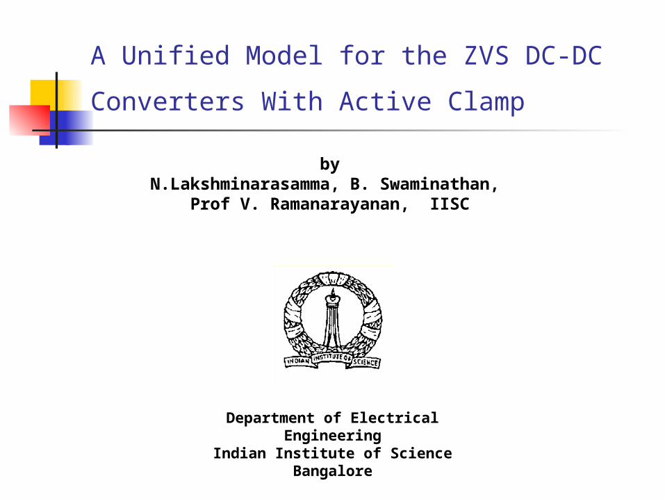
Typical Converter
Switches control power flow Reactive elements smoothen power flow Both are non-dissipative elements
LCSVg Vo

Classification of SMPS
SWITCHED MODE POWER
CONVERTERS
HARD SWITCHED POWER
CONVERTERS
SOFT-SWITCHED POWER CONVERTERS
Active Clamp Converters
Resonant Load Converters
Quasi-Resonant Converters
Resonant Transition Converters
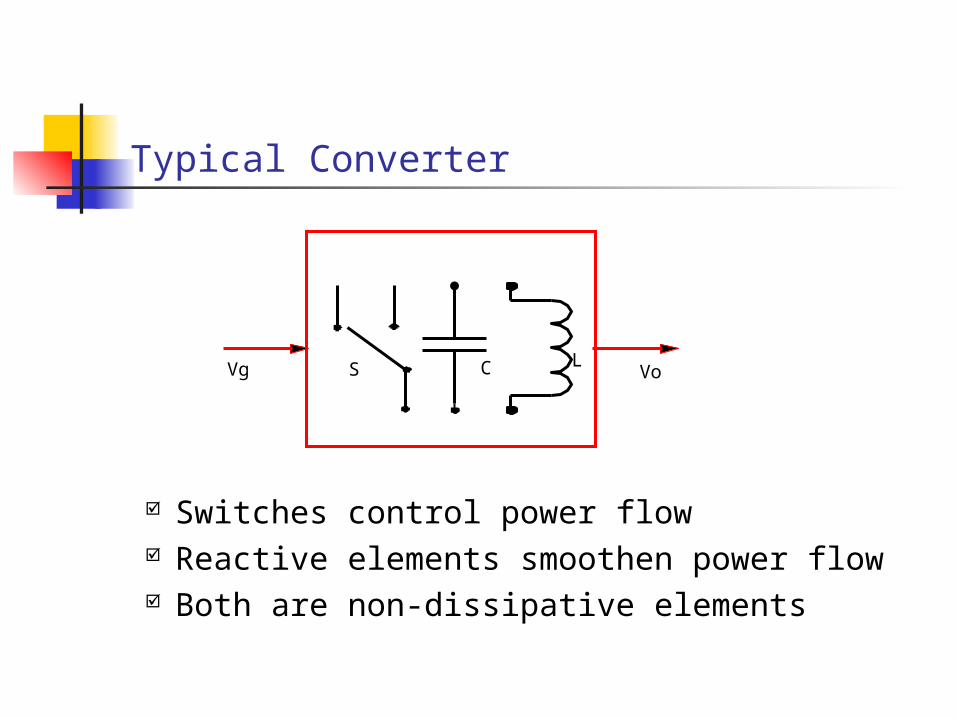
Hard Switching Converter
T1 T2
P
t
I
t V
I
V
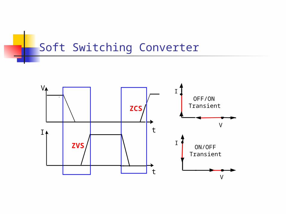
Soft Switching Converter
V
I t
t
ZVS
ZCS
I
V
I
V
OFF/ON Transient
ON/OFF Transient

Active Clamp ZVS Buck Converter
S2
S1
C R
CR
CC
LR I
D
V
DC
Throw1 Pole
CR
DClamp Capacitor
Clamp Switch
s2
LRS1
CR
+

Interval T1 - Zero-voltage Turn-on
*
R
Vi(t) I t
L
*
RI I
T1 LV
*1
Ns
T II 1
T I
IN - Normalized current
I
V VoS2S1
CRCR
D1
D2
LR
D
VCi(t)
i(0) = -I*
i(T1) = I

Interval T2 - Resonant Commutation
I
V VoS2S1
CRCR
D1
D2
LR
D
VC i(t)
i(0) = I
v(t) v(0) = V v(T2) = 0
R
R R R
C ti(t) I V sin
L L C
R R
tv(t) Vcos
L C
RT2R
Ci( ) I V
L
T2v( ) 0
R RT2 L C2
S S
R R
f fT2
Ts 2 2 f 4f

Interval T3 - Power-on Duration
I
V VoS2S1
CRCR
D1
D2
LR
D
VC i(t)
S1 turned off at end of T3 and CR almost instantly charges to V+VC.
R
R
Ci(t) I V
L T1 T2 T3 DTs T3 T1 T2
DTs Ts Ts

Interval T4 – Assisted Turn-off
I
V VoS2S1
CRCR
D1
D2
LR
D
VC i(t)
i(T4) = I
R C
R R
C V Vi(t) I V t
L L
T4i( ) I
RR
C R
V CT4 L
V V L
S
R
T4 1 f
Ts 1 2 f
CV
V

Interval T5 – Resonant Commutation
I
V VoS2S1
CRCR
D1
D2
LR
D
VC i(t)
v(0) = 0
v(T5) = V
RC
R R R
C ti(t) I V V sin
L L C
CR R
tv(t) V V 1 cos
L C
RT5R
CI( ) I V 1
L
V ( T5 ) = V
R RT5 L C cos1
1S
R
fT5cos
Ts 2 f 1
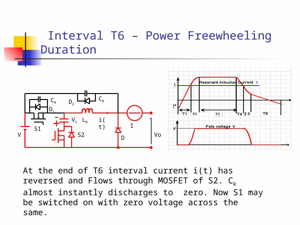
Interval T6 – Power Freewheeling Duration
At the end of T6 interval current i(t) has reversed and Flows through MOSFET of S2. CR almost instantly discharges to zero. Now S1 may be
switched on with zero voltage across the same.
I
V VoS2S1
CRCR
D1
D2
LR
D
VC i(t)
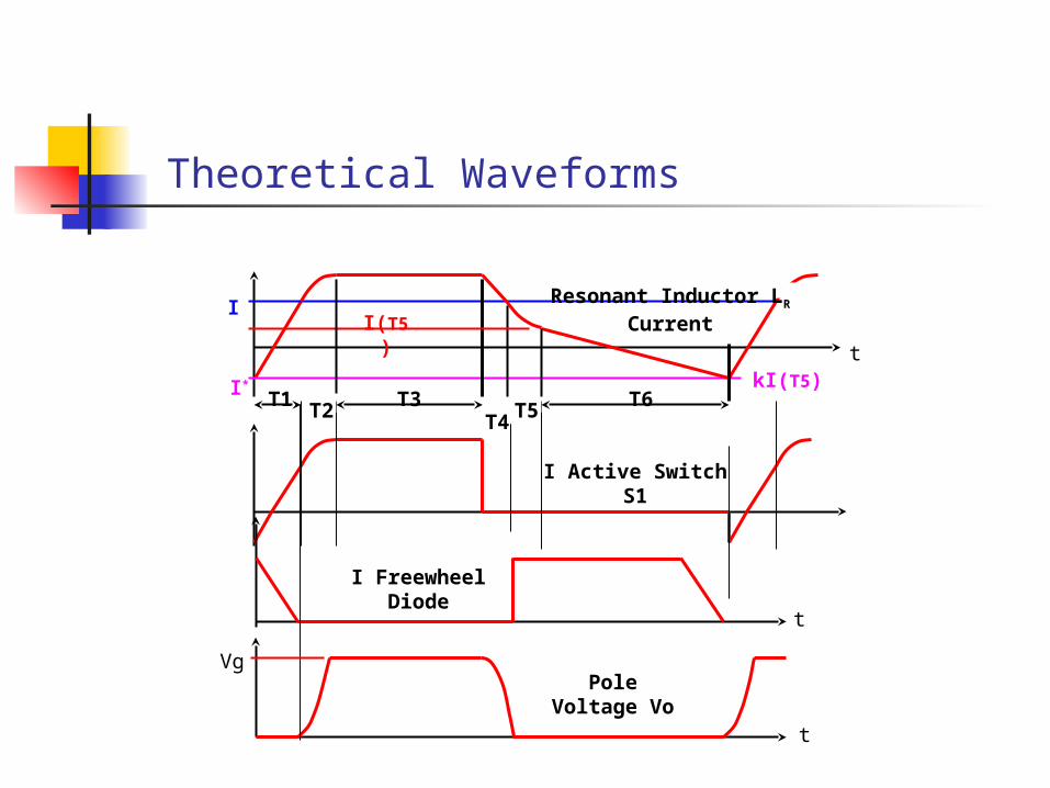
Theoretical Waveforms
I Active Switch S1
I*
T2T1 T3 T6
I
T4T5
t
I(T5)
kI(T5)
Resonant Inductor LR Current
I Freewheel Diode
t
Pole Voltage Vo
t
Vg
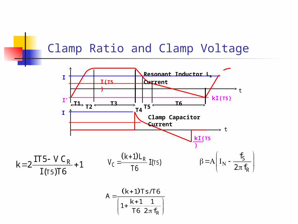
Clamp Ratio and Clamp Voltage
t
Clamp Capacitor CurrentI
kI(T5)
I*
T2T1 T3 T6
I
T4T5
t
I(T5)
kI(T5)
Resonant Inductor LR Current
R
T5
IT5 V Ck 2 1
I ( )T6
RT5C
k 1 LV I( )
T6
S
R
f
2 f
R
k 1 Ts / T6A
k 1 11
T6 2 f

Steady State Equivalent Circuit Model
1: D
(1+k)LR/Ts
Steady State Equivalent Circuit for Active Clamp Buck converter
o R
g g s
V L I(1 k)D
V V T
Ro g
s
L I(1 k)V DV
T

Equivalent Circuit Models of Other Converters
1-D: 1
Rd
1-D: 1 1:D
Rd
1: D1-D: 1
Rd1 Rd2
Equivalent circuits of the active clamped ZVS boost, buck-boost and cuk converters
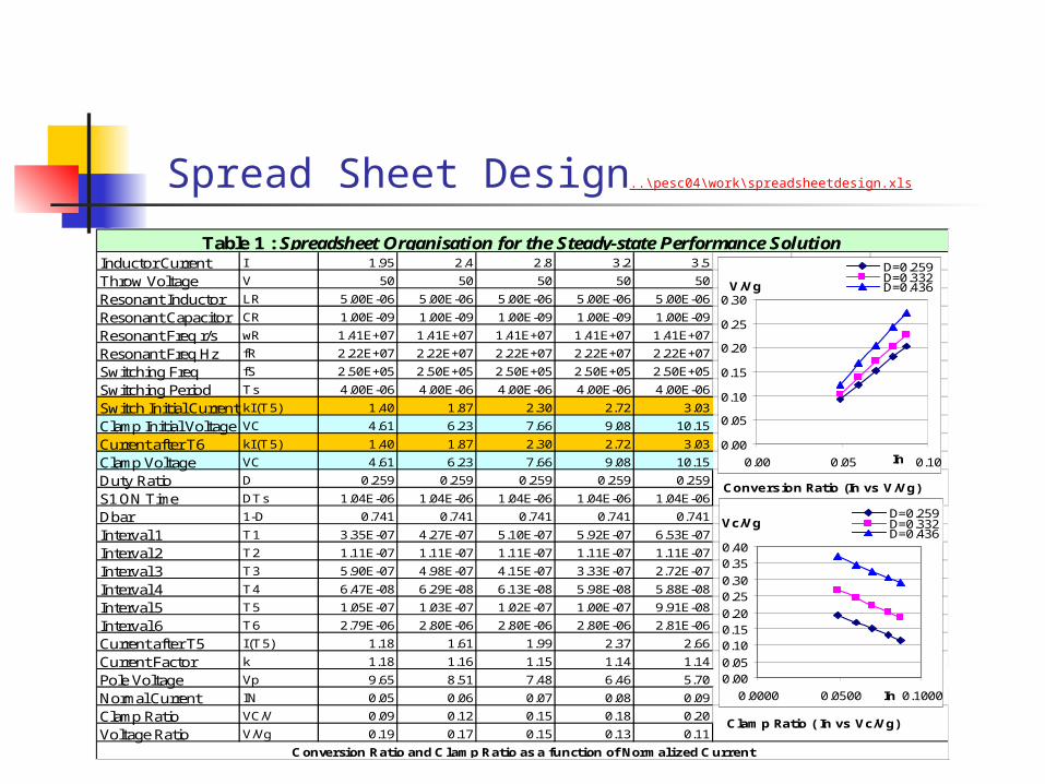
Spread Sheet Design..\pesc04\work\spreadsheetdesign.xls
Inductor Current I 1.95 2.4 2.8 3.2 3.5
Throw Voltage V 50 50 50 50 50
Resonant Inductor LR 5.00E-06 5.00E-06 5.00E-06 5.00E-06 5.00E-06
Resonant Capacitor CR 1.00E-09 1.00E-09 1.00E-09 1.00E-09 1.00E-09
Resonant Freq r/s wR 1.41E+07 1.41E+07 1.41E+07 1.41E+07 1.41E+07
Resonant Freq Hz fR 2.22E+07 2.22E+07 2.22E+07 2.22E+07 2.22E+07
Switching Freq fS 2.50E+05 2.50E+05 2.50E+05 2.50E+05 2.50E+05
Switching Period Ts 4.00E-06 4.00E-06 4.00E-06 4.00E-06 4.00E-06
Switch Initial Current kI(T5) 1.40 1.87 2.30 2.72 3.03
Clamp Initial Voltage VC 4.61 6.23 7.66 9.08 10.15
Current after T6 kI(T5) 1.40 1.87 2.30 2.72 3.03
Clamp Voltage VC 4.61 6.23 7.66 9.08 10.15
Duty Ratio D 0.259 0.259 0.259 0.259 0.259
S1 ON Time DTs 1.04E-06 1.04E-06 1.04E-06 1.04E-06 1.04E-06
Dbar 1-D 0.741 0.741 0.741 0.741 0.741
Interval 1 T1 3.35E-07 4.27E-07 5.10E-07 5.92E-07 6.53E-07
Interval 2 T2 1.11E-07 1.11E-07 1.11E-07 1.11E-07 1.11E-07
Interval 3 T3 5.90E-07 4.98E-07 4.15E-07 3.33E-07 2.72E-07
Interval 4 T4 6.47E-08 6.29E-08 6.13E-08 5.98E-08 5.88E-08
Interval 5 T5 1.05E-07 1.03E-07 1.02E-07 1.00E-07 9.91E-08
Interval 6 T6 2.79E-06 2.80E-06 2.80E-06 2.80E-06 2.81E-06
Current after T5 I(T5) 1.18 1.61 1.99 2.37 2.66
Current Factor k 1.18 1.16 1.15 1.14 1.14
Pole Voltage Vp 9.65 8.51 7.48 6.46 5.70
Normal Current IN 0.05 0.06 0.07 0.08 0.09
Clamp Ratio VC/V 0.09 0.12 0.15 0.18 0.20
Voltage Ratio V/Vg 0.19 0.17 0.15 0.13 0.11
Table 1 : Spreadsheet Organisation for the Steady-state Performance Solution
Conversion Ratio (In vs V/Vg)
Clamp Ratio ( In vs Vc/Vg)
Conversion Ratio and Clamp Ratio as a function of Normalized Current
0.000.05
0.100.150.20
0.250.30
0.350.40
0.0000 0.0500 0.1000In
Vc/VgD=0.259D=0.332D=0.436
0.00
0.05
0.10
0.15
0.20
0.25
0.30
0.00 0.05 0.10In
V/Vg
D=0.259D=0.332D=0.436
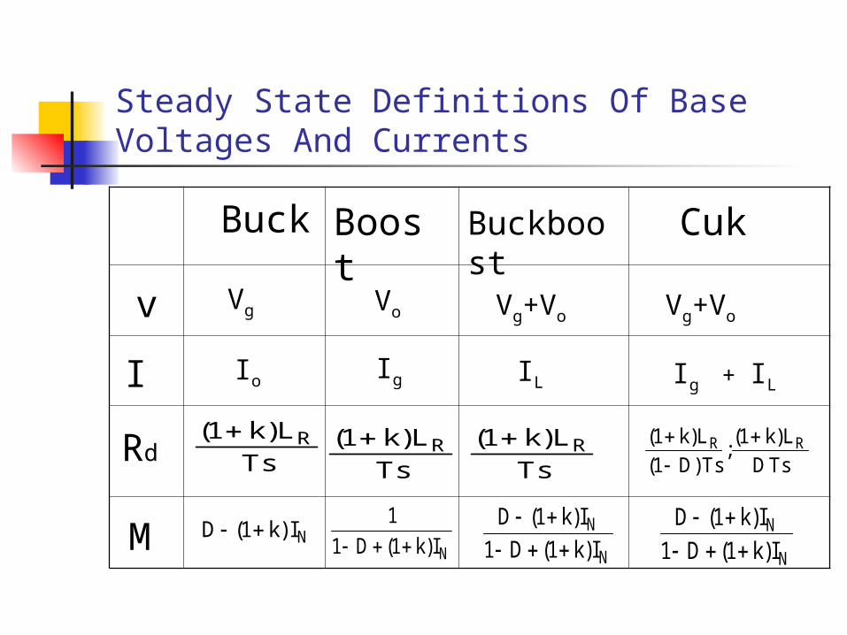
Steady State Definitions Of Base Voltages And Currents
Buck Boost Buckboost Cuk
v
Rd
M
IVg
Io
R(1 k)L
Ts
ND (1 k) I
Vo
Ig
R(1 k)L
Ts
R(1 k)L
Ts
N
1
1 D (1 k)I
IL
N
N
D (1 k)I
1 D (1 k)I
N
N
D (1 k)I
1 D (1 k)I
R R(1 k)L (1 k)L;
(1 D)Ts DTs
Ig + IL
Vg+Vo Vg+Vo

Dynamic Model Of Active Clamp Buck Converter
Perturbation of the nonlinear circuit averaged model about a quiescent operating point.
ˆ ˆD+d I+ig gˆV +V
L
+-+
1:D
Rc
C
-+ g g
ˆ ˆD+d V +V
R
S
(1+k)L
T
Small signal ac model of active clamp buck converter
1:D
R
S
(1+k)L
T
Rc
L
CR
gd̂V
D
d̂IgV̂-
-
+
+
+-

Simulated Active Clamp Buck Converter
0
G1
S1
G2
1n
7u
1n
MUR1620CT
5u
IRF250150u
MUR1620CTIRF25050V
110u
12
Output power = 60 watts
Input voltage = 50 volts
Output voltage = 20 volts
Switching frequency = 250 KHz

Resonant Inductor Current Waveform
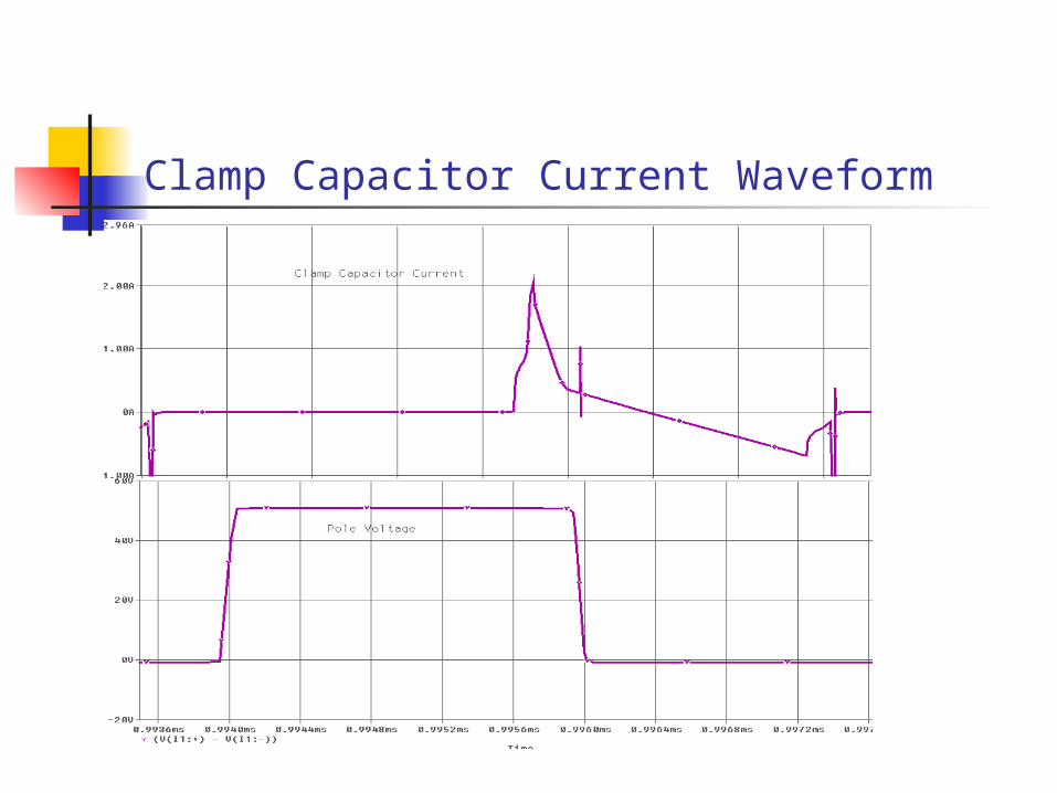
Clamp Capacitor Current Waveform

Steady State Performance Of Active Clamp Buck Converter
Clam p Ratio
0.00
0.10
0.20
0.30
0.40
0.50
0.60
0.00 0.05 0.10 0.15
In- Am ps
Vc
/Vg D=0.259
D=0.332D=0.436
Clam p Ratio
0.00
0.10
0.20
0.30
0.40
0.50
0.60
0.00 0.05 0.10 0.15In- Am ps
Vc
/Vg D=0.259
D=0.332D=0.436
Conversion Ratio
0.00
0.10
0.20
0.30
0.40
0.50
0.00 0.05 0.10 0.15In- Am ps
V/V
g
D=0.259D=0.332D=0.436
Conversion ratio
0.00
0.10
0.20
0.30
0.40
0.50
0.00 0.05 0.10 0.15IN - Am ps
V/V
g
D=0.259D=0.332D=0.436
SIMULATED RESULTS EXPERIMENTAL RESULTS

Experimental Waveforms Of Active Clamp Buck Converter
Vgs and Vds of S1 showing ZVS; Vgs and Vds of S2 showing ZVS

Experimental Waveforms Of Active Clamp Buck Converter
Pole voltage and Inductor current waveforms; Pole voltage and Clamp capacitor current waveforms
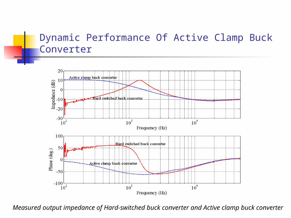
Dynamic Performance Of Active Clamp Buck Converter
Measured output impedance of Hard-switched buck converter and Active clamp
buck converter
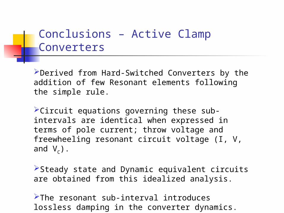
Conclusions – Active Clamp Converters
Derived from Hard-Switched Converters by the addition of few Resonant elements following the simple rule.
Circuit equations governing these sub-intervals are identical when expressed in terms of pole current; throw voltage and freewheeling resonant circuit voltage (I, V, and VC).
Steady state and Dynamic equivalent circuits are obtained from this idealized analysis.
The resonant sub-interval introduces lossless damping in the converter dynamics.
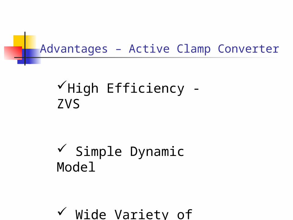
Advantages – Active Clamp Converter
High Efficiency - ZVS
Simple Dynamic Model
Wide Variety of Topologies

Thanks


![Survey stability of the ZVS phase-shifted full-bridge DC ...journal.it.cas.cz/62(2017)-KHO/Paper Sharif260.pdf · ZVS PWM in [4] is formed by a diode, a resonant capacitor and a resistor.](https://static.cupdf.com/doc/110x72/5e3125c4d23e5149907b5255/survey-stability-of-the-zvs-phase-shifted-full-bridge-dc-2017-khopaper-sharif260pdf.jpg)


![Fuzzy Controlled ZVS Asymmetrical PWM Full-bridge DC-DC ... · robust fuzzy logic controller and fuzzy load conductance observer for DC-DC boost converter is designed [16]. State](https://static.cupdf.com/doc/110x72/5f4a3cdbda168c151e4e1cc6/fuzzy-controlled-zvs-asymmetrical-pwm-full-bridge-dc-dc-robust-fuzzy-logic-controller.jpg)