Proceedings of the Asia-Pacific Microwave Conference 2011
A Matrix-Computation Based Methodology for Extracting the S-Parameters of Interconnects in Advanced Packaging Technologies
Yin-Cheng Changl,2, Da-Chiang Changl, Shawn S. H. Hsu2, Member, IEEE, Jeng-Hung Leel, Shuw-Guann Linl, and Ying-Zong Juangl
I Chip Implementation Center, National Applied Research Laboratories, Hsinchu, Taiwan 2Institute of Electronics Engineering, National Tsing Hua University, Hsinchu, Taiwan
Abstract - A reliable method is proposed to extract the Sparameters of the vertical interconnects which normally could not be obtained directly with measurement. This kind of vertical interconnect includes bumpers and through-silicon-vias (TSVs) popularly used in advanced packaging. The proposed method, composed of designing structures and processing matrix, exhibits its validity over a wide range of frequency. The bump appearing in flip-chip assembly is utilized as an example of which the Sparameters are extracted. The equations and the measurement procedure making up the method are reported in detail.
Index Terms -extraction; de-embedding; interconnect; bump; TSVs.
I. INTRODUCTION
For high density and high operating frequency demand,
high performance packaging technologies like System-in
Package (SiP) and 3D-ICs become more and more popular.
Accompany with the quality of their interconnects as shown in
Fig. 1, such as the bond-wires, bumps and TSVs, becomes
more and more critical, because of the effect they contribute
to the system. While lots of the improved technologies were
proposed to keep these parasitic low [1]-[2] and various
mature characterizations [3]-[6] were presented to extract and
model bond-wires, vias, devices, and transmission lines in
different applications, there is a relative low amount of
literature published to focus on the de-embedding method of
the interconnects.
Four different measurement approaches [7] were used to
extract the parasitic inductance of TSV. They applied the
Line-Reflect-Reflect-Match (LRRM) calibration to shift the
reference plans to the test structures firstly. Then it took the
advantage of measuring the resonance frequency after adding
series or shunt resonators. The constant inductance of TSV
can be derived eventually by summarizing various test
structures which consisted of resonators. Except for the half
wavelength resonator approach, the measured results from the
other approaches would be sensitive to the probe placement
and the calibration accuracy. And only an inductance value
was extracted, such a single lumped model may be
insufficient for high frequency prediction. Leung [8] proposed
a simple short structure and utilized the half wavelength
approach to build up an accurate equivalent-circuit model,
which composed of not only the inductance but the resistance
Bond Wire
Micro-bump Si-sub2
Si-sub 1
�TSV
Si-sub 2 lSi-sub 1
Fig. 1. Typical vertical interconnects in advanced packaging technologies.
of the through wafer interconnect (TWI) up to 200Hz. A
minor concern is the applicable bandwidth of the half
wavelength structure which is frequency dependent. And the
extracted S-parameters from one-port measurement can not be
directly used in the circuit simulation. Ryu [9] proposed an
advanced two-port model composed of RLCO components.
The extracted parameters were much useful for RF circuit
integration. Their unique measurement was to place one probe
on the top of via directly and to place the other probe on the
CPW line which was connected to the bottom side of via. The
via can be extracted from a simple de-embedding method like
port extension or (Through-Reflect-Line) TRL. This method
is simple and straightforward, but will face difficulty if the
interconnect under test, like the bumps in the flip-chip process,
can not be contacted directly.
The most straightforward method to obtain the two-port S
parameters of an interconnect is to contact microwave probes
at two ends of the interconnect directly. In practice, there are
some tasks have to be overcome. Take the TSV for example,
the two ends of TSV are not at the same plane, but most
developed testing facilities, such as probe stations, were
designed to deal with the issues at the same plane nowadays.
Therefore, one interesting idea is to raise the wafer to a
vertical position, and then move the horizontal probes to land
on two ends of the TSV at two sides. In this solution, the
wafer handler might be a task to be solved. And it faces a
further difficulty; all the testing results could be meaningless
without calibration. A set of double side calibration kits with
well-defined standards is the way to realize calibration. But it
might become a customized product, the process of
978-0-85825-974-4 © 2011 Engineers Australia 1909

, , , ,
x ·t----� y ·---t -� x
( _� _______ J. ) : i " ,:- 1 :
. '
x 0.
.-:
: �::�::.�
Fig. 2. Vertical interconnect with horizontal track in the deembedding method.
implementation and the expense could be the problems before
mentioning its accuracy. Another idea based on the existing
planar calibration is try to land one probe on the top side of
TSV and flip another probe to the bottom side of the wafer to
make contact. The other idea is to lift both the probe
positioners and the wafer to be vertical after a regular planar
calibration, and then make contact on the TSV. The latter two
solutions could be feasible without needing a new calibration
standard under development. But they remain the risk of
suffering from high uncertainty during moving the probe
positioners after calibration. For these reasons, the 3D testing
was put away in this paper and turned the testing solutions
back to the indirect extraction.
In this paper, a de-embedding methodology for extracting
two-port S-parameters is proposed. A case of the bump in flip-chip process is utilized as an example. But this method
can deal with most kind of interconnects including bond-wire,
micro-bump and TSV with certain purposely designed
structures. The following sections depict the method and the
experiment results verify the feasibility.
II. METHODOLOGY
A certain structure as shown in Fig. 2 is proposed to explain
the idea of extracting the characteristics of interconnect.
Along the signal path, the signal flows into the interconnect
on the left side from the bottom layer, then passes through the
track on the top layer. And it eventually goes back to the
bottom layer via the interconnect on the right side.
Mathematically, the S parameters of the structure are
determined by those of the three elements and matrix handling.
In this case, the T -matrix was chosen to represent the
properties of the elements because the T-matrix is suitable for
matrix calculation given a structure where the signal flows
through each element in series. With the symbols X and Y
denote the T -matrix of the vertical interconnect and the
horizontal track connecting the two vertical interconnects,
respectively, two matrixes are defined as following.
Tl =Y T2=X·Y·X
(I)
(2)
where T2 represents the structure as shown in Fig. 2. If the
matrix TI is given decisively, the matrix X representing the
vertical interconnect could be derived by following the steps
described below,
T2·Tl =XYX· Y (3)
-1.0 + +
iii' � -1.5 + N (f) -2.0
--X_sim. -2.5 ;- Y _sim. + +
-XYX_sim.
-3.0 0�==:1� 0=�2� 0=�3:::- 0 -----740=----::50::---6�0::------:!70 Freq (GHz)
Fig. 3. Validity of the methodology from verifying the insertion losses.
(a) (b) Fig. 4. Photos of the flip-chip technology: (a) top view by the alignment prism, (b) side view of the bonding process.
'-"T2Tl =XY X = '-"T2T1 . y-I
(4)
(5)
For the validation of the method, a virtual experiment was
carried out in simulation first. The equivalent model proposed
in [9] was applied to represent the interconnect associated
with X. And a transmission line was utilized to model the
track associated with Y. The three matrix, Tl, T2, and X, are
obtained with simulation. Following (3), (4), and (5) derives
another version of X which is an extracted result. The
insertion loss (S21) related to the four matrixes are calculated
and shown in Fig. 3. The line X_sim and the line X_extracted
are the insertion losses associated with the two X obtained in
different ways. Their good agreement demonstrates the
proposed method is capable of extracting the S-parameters of
the interconnect precisely. Moreover, the method is reliable
over a wide range of frequency without generating any
singularity. This method can be applied to any vertical
interconnect in the technology that is able to form the
configuration as shown in Fig. 2. The following section is a
practical experiment in which the design of the de-embedding
patterns to obtain Tl and T2, and the detailed procedures to
extract the final X are described.
III. EXPERIMENTAL PROCEDURE AND RESULTS
A typical flip-chip assembly technology is adopted to
demonstrate the whole experiment in this work. The SnI Ag
bumpers connect the chip manufactured by the standard
TSMC IP6M O.18um CMOS process to the glass substrate of
an integrated passive device (GIPD) process. The top CMOS
1910
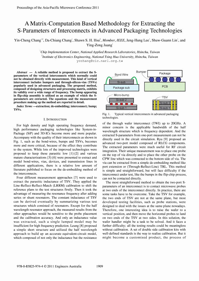
CMOStotal CMOSopen
T1 Fig. 5. De-embedding patterns for extracting Tl.
·1.0
iiJ � ·1.S c::i !J) -2.0r ,---------,
-- T1_EM sim.
-2.S --- T1_extracted
- CMOStotal_meas.
-3. 0 0l-===::::;1 =0 ==::::::;:20== == 3::;:0==�4�0-�SO--6""'0---.J 70
Freq (GHz) Fig. 6. Comparison of the insertion losses between simulation and measurement related to Tl.
chip and the bottom glass substrate form a face-to-face
configuration as shown in Fig. 4. The transmission lines used
in the experiment are coplanar waveguide (CPW) type owing
to its popular usage in RF and microwave designs. Besides,
each ground-signal-ground structure is designed to maintain
its characteristic impedance of 50 ohms to reduce the
mismatch on the interfaces. As a result, each structure
diminishes the uncertain effects caused by varied ground
reference, for example. The full wave electromagnetic (EM)
simulation of the drawn patterns in this work was performed
by ADS MOMENTUM™. And the vector network analyzer
used in the measurement is Agilent E8361A PNA with the
range of frequency lOMHz-67GHz.
Following the derivation procedure described in last
section, the matrix Tl and T2 have to be obtained prior to the
step extracting the S-parameters of the bumps. As all the
measurements are on-wafer level, probing pads extended from
the structures related to Tl and T2 are reserved for testing
and their effects should be removed afterwards. Therefore,
extra patterns as shown in Fig. 5 and Fig. 7 are used in the
first-tier de-embedding. The track between the two bumps and
the probing pads on the top chip were implemented in CMOS
process and named as CMOStotal. The matrix Tl can be
simply obtained by using an extra open kit structure
(CMOSopen) as shown in Fig. 5. All the measured data were
transformed into Y-matrix in order to remove the parasitic
effects of the probing pads with the equation as shown below.
[Tl]y = [CMOStotal]y - [CMOSopen]y (6)
1911
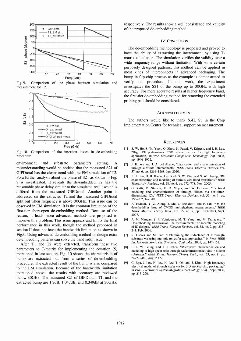
GIPDtotal GIPDopen
GIPDshort T2 Fig. 7. De-embedding patterns for extracting T2.
0.0 '"""--.-----,--.,.--�--.,.._--.----, -O .S ·1.0 ·1.S ·2.0
� ·2.S !g ·3.0 � ·3.S !J) .4.0
·4.S ·S.O -S.S
-- T2_EM sim.
-GIPDtotal_meas. --- T2_extracted
T2_de. open
-6. 0 0!:-===::::;1�0==�2� 0 ==�30�=- 47.0::-----'S=-=0 :-----'6�0---:!70 Freq (GHz)
Fig. 8. Comparison of the insertion losses between simulation and measurement related to T2.
The results shown in Fig. 6 depict the S21 related to Tl
after removing the effects of the probing pad. The EM
simulation has a good agreement with that resulting from
measurement which means the parameters set in EM
environment are accurate. For T2, because the CMOS chip
was flipped, the 50 ohms CPW lines on glass substrate were
utilized to locate the probing pad out from bumps to a proper
distance for testing. The structure with extended probing pad
was defined as GIPDtotal as shown in Fig. 7. And it leads to
not only the open pad pattern (GIPDopen), but one more de
embedding short pattern (GIPDshort) to be needed for de
embedding the serial parasitic of CPW lines and moving the
reference plane to the bumps. This first-tier de-embedding is
so-called short-open de-embedding method which is popular
in most device modeling procedure. Both the GIPDtotal and
GIPDshort should take off the parallel parasitics of open pad
in Y -matrix form. Then transform the Y -matrix to the Z
matrix representaion, the parasitic of short pattern can be
subtracted from GIPDtotal and obtain T2 eventually. The
detailed equations were described as below.
[T2/open]y = [GIPDtotal]y-[GIPDopen]y (7)
[GIPDshort/open] = [GIPDshort]y - [GIPDopen]y (8)
[T2Jz = [T2/openJz - [GIPDshort/openJz (9)
The results as shown in Fig. 8 indicate the T2 was
extractedout from the probing pad. The difference between
extracted result and simulated result comes from the EM
200rr===�===c==�----�--�--=c---' 150 -GIPDtotal
-- T2_EM sim.
Q) 100 ---e- T2_extracted
� C) 50 CI> � 5l <U .t: '1 N -100
en -150
-2oooL----1� 0--�2� 0----3�0�--4�0�--�50�--�60�--�70 Freq (GHz)
Fig. 9. Comparison of the phase between simulation and measurement for T2.
-1 .0
iii � -1.5
L1 -2.0 ---e- X_extracted
-2.5 Y _extracted
-XYX w/i pad meas.
-3.0�=�===::====::-::==-o!..-7-::"--�::--�"!-=----:! o 10 20 30 40 50 60 70 Freq (GHz)
Fig. 10. Comparison of the insertion losses in de-embedding procedure.
environment and substrate parameters setting. A
misunderstanding would be noticed that the measured S21 of
OIPDtotal has the closer trend with the EM simulation of T2.
So a further analysis about the phase of S21 as shown in Fig.
9 is investigated. It reveals the de-embedded T2 has the
reasonable phase delay similar to the simulated result which is
differed from the measured OIPDtotal. Another point is
addressed on the extracted T2 and the measured OIPDtotal
split out when frequency is above 300Hz. This issue can be
observed in EM simulation. It is the common limitation of the
first-tier short-open de-embedding method. Because of the
reason, it leads more advanced methods are proposed to
improve this problem. This issue appears and limits the final
performance in this work, though the method proposed in
section II does not have the bandwidth limitation as shown in
Fig.3. Using advanced de-embedding method or design extra
de-embedding patterns can solve the bandwidth issue.
After T1 and T2 were extracted, transform these two
parameters to T-matrix for implementing the equation (5)
mentioned in last section. Fig. 10 shows the characteristic of
bump are extracted out from a series of de-embedding
procedure. The extracted result of the bump is also compared
to the EM simulation. Because of the bandwidth limitation
mentioned above, the results with accuracy are reviewed
below 300Hz. The measured S21 of OIPDtotal, T1, and the
extracted bump are 1.7dB, 1.047dB, and O.349dB at 300Hz,
respectively. The results show a well consistence and validity
of the proposed de-embedding method.
IV. CONCLUSION
The de-embedding methodology is proposed and proved to
have the ability of extracting the interconnect by using T
matrix calculation. The simulation verifies the validity over a
wide frequency range without limitation. With some certain
purposely designed patterns, this method can be applied in
most kinds of interconnects in advanced packaging. The
bump in flip-chip process as the example is demonstrated to
verify this procedure. In this work, the experiment
investigates the S2l of the bump up to 300Hz with high
accuracy. For more accurate results at higher frequency band,
the first-tier de-embedding method for removing the extended
probing pad should be considered.
ACKNOWLEDGEMENT
The authors would like to thank S.-H. Su in the Chip
Implementation Center for technical support on measurement.
REFERENCES
[I] S. W. Ho, S. W. Yoon, Q. Zhou, K. Pasad, V. Kripesh, and J. H. Lau, "High RF performance TSV silicon carrier for high frequency application," in Proc. Electronic Components Technology Conf, 2008, pp. 1946-1952.
[2] J. H. Wu and J. A. del Alamo, "Fabrication and characterization of through-substrate interconnects," IEEE Trans. Electron Devices, vol. 57, no. 6, pp. 1261-1268, Jun. 2010.
[3] J. H. Lim, D. H. Kwon, J.-S. Rieh, S. W. Kim, and S. W. Hwang, "RF characterization and modeling of various wire bond transitions," IEEE
Trans. Adv. Packag., vol. 28, no. 4, pp. 772-778, Nov. 2005.
[4] G. Katti, M. Stucchi, K. D. Meyer, and W. Dehaene, "Electrical modeling and characterization of through silicon via for threedimensional ICs," IEEE Trans. Electron Devices, vol. 57, no. I, pp. 256-262, Jan. 2010.
[5] A. Issaoun, Y. Z. Xiong, J. Shi, J. Brinkhoff, and F. Lin, "On the deembedding issue of CMOS multigigahertz measurements," IEEE Trans. Microw. Theory Tech., vol. 55, no. 9, pp. 1813-1823, Sept. 2007.
[6] A. M. Mangan, S. P. Voinigescu, M. T. Yang, and M. Tazlauanu, " De-embedding transmission line measurements for accurate modeling of IC designs," IEEE Trans. Electron Devices, vol. 53, no. 2, pp. 235-241, Feb. 2006.
[7] R. Us cola and M. Tutt, "Determining the inductance of a throughsubstrate via using multiple on-wafer test approaches," in Proc. IEEE Int. Microelecronic Test Structures Conf, Mar. 2001, pp. 147-151.
[8] L. L. W. Leung, and K. J. Chen, "Microwave characterization and modeling of high apect ratio through-wafer interconnect vias in silicon substrates," IEEE Trans. Microw. Theory Tech., vol. 53, no. 8, pp. 2472-2480, Aug. 2005.
[9] C. Ryu, J. Lee, H. Lee, K. Lee, T. Oh, and J. Kim, "High frequency electrical model of through wafer via for 3-D stacked chip packaging," in Proc. Electronics Systemintegration Technology Conf, Sept. 2006, pp. 215-220.
1912