7D-ia9 311 GROUD BSED rH IGH POWER HICROIAE DECOY DISCRIMINATION l,
SYSTEN(IJ) HUGHES RESEARCH LASS MALIBU CAECKHAlRDT ET AL 23 DEC 87 H4AC-REF-GA656
UNCLAS7SIFIED N881486 C-8878 F/ 19/12 ML
I~l~rn ~112811-5
,3,
111111-2 11111-
MICROCOPY RESOLUTION TEST CHARTNATIONAL BUREAU OF STANOARDS-1963-A
10

HAC REF. G0656
GROUND-MBASEDHIGH-POWER MICROWAVEDECOY DISCRIMINATION SYSTEM
Wllfried 0. Eckhardt, Frank Chilton, Frank A. Dolezal, John 1. Generosa, Robin J. Harvey,SA. Jay Palmer, Gary A. Saenz, James G. Small, and Weldon S. Williamson(V)
Hughes Research Laboratories
00 3011 Malibu Canyon Road
V Malibu, California 90265
N ~ December 1987
Technical Progress Report No. 2
Contract N00014-86-C-0878
January 1, 1987 through December 31, 1987
Sponsored by:OFFICE OF NAVAL RESEARCH DTIC800 N. Ouincy Street EL CT EArlington, VA 22217-5000 DEC 3 01987
Monitored by:
Dr. Howard E. Brandt
Department of the Army
Harry Diamond Laboratories
2800 Power Mill Road
Adelphi, MD 20783 j:" ; .
'" + <" "87 ...2+ / ,

UNCLASSIFIED;ECURITY CLASSIFICATION OF THIS PAGE
I Form ApproveREPORT DOCUMENTATION PAGE O No,. 0704-0188
Ia. REPORT SECURITY CLASSIFICATION lb. RESTRICTIVE MARKINGS
Unclassified2a. SECURITY CLASSIFICATION AUTHORITY 3. DISTRIBUTION /AVAILABILITY OF REPORTDoD Instruction No. 5210.72 (3/15/83)
2b. DECLASSIFICATION/ DOWNGRADING SCHEDULE
i N/A IS M NT R G O G IA O RE R NU E(.. PERFORMING ORGANIZATION REPORT NUMBER(S) S, MONITORING ORGANIZATION REPORT NUMBER(S)
ia. NAME OF PERFORMING ORGANIZATION 6b. OFFICE SYMBOL 7a. NAME OF MONITORING ORGANIZATION
Hughes Research Laboratories (if applicable) Dr. Howard E. Brandt_I ._eDartmen__ of the Army
6c. ADDRESS (City, State, and ZIPCode) 7b. ADDRESS(City, State, and ZIP Code)I Harry Diamond Laboratories
3011 Malibu Canyon Road 2800 Powder Mill Road
I Malibu, CA 90265 Adelphi, MD 20783
NM SLCHD-NW-RA3. NAME OFFUNDING/SPONSORING 8b OFFICE SYMBOL 9 PROCUREMENT INSTRUMENT IDENTIFICATION NUMBER
.ORGANIZATION I(if applicable)Office of Naval Research
I 8c. ADDRESS (City, State, and ZIP Code) 10. SOURCE OF FUNDING NUMBERS
PROGRAM PROJECT TASK WORK UNIT800 N. Quincy Street ELEMENT NO. NO. NO. CCESSION NO.
* Arlington, VA 22217-5000:1. TITLE (Include Security Classification)
, -' Ground-Based High-Power Microwave Decoy Discrimination System12. PERSONAL AUTHOR(S)
-W.0. Eckhardt• 'I 3a. TYPE OF REPORT 13b. TIME COVERED 114 DATE OF REPORT (Year, Month, Day) 15. PAGE COUNT
. Technical Summary FROM I/I/87 T02/31184 1987 December 23 99
16. SUPPLEMENTARY NOTATION
'7/ COSATI CODES 18. SUBJECT TERMS (Continue on reverse if necessary and identify by block number)
~ FILD /GROP SU-GROP IDecoy Discrimination, High-Power Microwave, Ballistic\Missile Defenser ..46-?
1-9. ABSTRA (Continue on reverse of necessary an identify by block number) (*1.c The objectives of the subject contract are to conduct a detailed investigation of the
. . . feasibility of a ground-based high-power microwave decoy discrimination system. to explorekey technology items required for the implementation of such a system, and to design a
S prototype system. If an effective defense against a massive strategic missile attack is tobecome feasible, one of the important problems that must be solved is to devise a systemcapable of reliable discrimination between decoys and reentry vehicles. In principle, high-power microwaves (HPMs) can be expected to provide an effective discrimination mechanism.The most important features of the concept are (1) all aspects of the system. with thepossible exception of long-range sensors. are ground-based. yet there is an all-weather
* . capability: (2) HPM/target interactions can be studied in ground-based experiments: andI (3) the system hardware is expected to be highly modular and thus a enable to upgrading /
in several stages, based on successful testing. . -_, f.' ' , --j. - ' . , ,
'10 DISTRIBUTION/AVAILABILITY OF ABSTRACT 121 ABSTRACT SECURITY CLASSIFICATION
I [ ]UNCLASSFIED/UNLIMITED - SAME AS RPT Q DTIC USERS I Unclassified?a NAME OF RESPONSIBLE INDIVIDUAL 22b TELEPHONE (Include Area Code) 22c. OFFICE SYMBOL
W.O. Eckhardt (213) 317-5253DD Form 1473, JUN 86 Previous editions are obsolete. SECURITY CLASSIFICATION OF THIS PAGE
UNCLASSIFIED

UNCLASSIFIEDSECURITY CLASSIFICATION OP THIS PAGE
19. (Continued)
The effort this year has again resulted in a considerably increased understanding ofthe critical issues affecting the feasibility of the proposed ground-based HPM decoydiscrimination system. We have shown that the predicted damage mechanism can beproduced in high vacuum, and that the experiments agree with the predictions of ourHPM/target interaction model. We have proposed a mechanism that might enable theproduction of measurable thrust reactions from decoys with much thicker metal coatings thanwhat was previously thought to be feasible. We have established bounds on some importantparameters of the antenna system. and potential solutions to the single most criticalproblem - the cost of the large phased-array antenna -have been identified.
Accession For 'ff
*NTIS GRA&I F-DTIC TAB EJUnannounced! Just if feat ion
ByDistribution/
Availability Codes
Avsil and/or
Dist Special
,top
UNCLASSIFIEDSECURITY CLASSIFICATION OF THIF PAGE
I-I€
/ jr ' ,f'...

TABLE OF CONTENTS
* SECTION PAGE
1 INTRODUCTION .................................... 1......1
2 DISCRIMINATION CONCEPT DESCRIPTION ................. 5
2.1 Approach ................................... 5......5
2.2 Discrimination Mechanisms ....................... 8
2.2.1 Changes in Optical and MicrowaveSignatures, Including ChaffDestruction ............................. 9
2.2.2 Changes in Velocity Vector Causedby Vaporization Thrust ................. 9
3 PROGRESS. .................................... 11
3.1 Tasks 1-3: Theoretical Study ofHPM/Target Interactions ....................... 11
3.1.1 Direct-Heating Model .................... 12
3.1.2 Electron-BombardmentHeating Model ........................... 18
3.2 Tasks 4-6: Experimental Study of
HPM/Target Interactions ....................... 27
3.2.1 Experimental Apparatus ................. 27
3.2.2 Test Results ............................ 29
3.2.3 Comparison with AnalyticalModel ................................... 34
3.2.4 Limitations of PresentApparatus ............................... 34
3.2.5 Planned Apparatus Revisions ......... 36
, 3.3 Task 7: Survey of the State of theArt in HPM Technology ......................... 38
3.3.1 Virtual-Cathode (VC) Devices ........ 39
~iii
I, ~~~~~ p w * , - p .? * " i'- , ." - ." - m

SECTION PAGE
3.3.2 Free-Electron Lasers (FELs)and Cyclotron Masers (CMs) ............ 41
3.3.3 Back-Wave Oscillators (BWOs) ........ 42
3.3.4 Cross-Field Oscillators/Amplifiers (CFOs/CFAs) ................. 42
3.3.5 Cavity Compression ..................... 44
3.3.6 Summary ................................. 44
3.4 Tasks 8-10: System Design Study ............. 45
3.4.1 Phased-Array Beam Steeringand Focusing ........................... 45
3.4.2 The Effects of Aperture Thinningand Phase Errors on a LargePhased-Array Antenna ................... 58
3.5 Tasks 17-18: High-Power Phase-ShifterConcept Exploration ........................... 70
3.5.1 Phase-Shifter Arrays ................... 70
3.5.2 Magnetic Field Antennas ............... 87
3.5.3 Electric Field Antennas ............... 90
4 CONCLUSIONS .................................... 93
REFERENCES .................................... 95
i

I
LIST OF ILLUSTRATIONS
FIGURE PAGE
1 Ground-based HPM decoy discriminator ............ 6
V- 2 Ground-based HPM engagement rangesto midcourse targets ................................ . 7
3 Microwave heating and thrusting ofaluminized foils: theoreticallymodeled phenomena ................................... 13
4 Short-pulse theoretical results for aluminum .... 17
5 Long-pulse theoretical results for aluminum ..... 19
6 Experimental apparatus .............................. 28
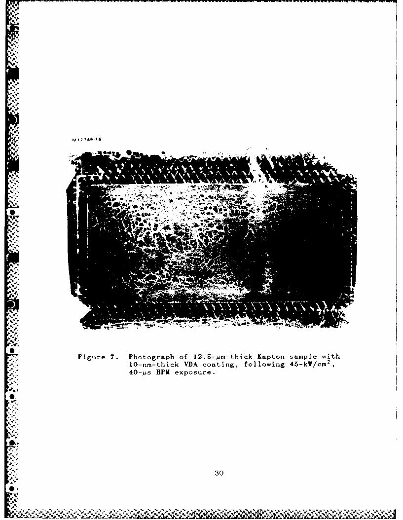
7 Photograph of 12.5-#m-thick Kapton sample with10-nm-thick VDA coating, following 45-kW/cm 2 ,40-ps HPM exposure .................................. 30
8 Photograph of 12.5-Mm-thick Kapton sample with10-nm-thick VDA coating, following 44-kW/cm2 ,4 0 -ps HPM exposure .................................. 31
9 Photograph of 12.5-Mm-thick Kapton sample with20-nm-thick VDA coating, following 68-kW/cm2 ,40-ps HPM exposure .................................. 32
10 Photograph of 12.5-Mm-thick Kapton sample with50-nm-thick VDA coating, following 42-kW/cm 2,4 0-Ms HPM exposure .................................. 33
11 Revised system ....................................... 37
12 A single array element has a wide fieldof illumination ...................................... 50
13 Extended arrays can form narrow beams whenthe contributions from each element arrivein phase at a distant point ........................ 51
14 The transmitted beam may be steered to theright by progressively phase shifting thediscrete elements of the array ..................... 53
V

FIGURE PAGE
15 For large ranges R, converging sphericalwavefronts differ from plane waves by lessthan 1/10 wave over relatively large areas ...... 57
16 Irradiance pattern for uniformly illuminatedcircular aperture ................................... 60
17 Irradiance pattern for centrally obscured
circular aperture ................................... 62
18 Array of 64 small circular subapertures ......... 63
19 Array of 16 circular subapertures ................. 64
20 Far-field patterns of case A(diffraction-limited) ............................... 65
21 Far-field patterns of case B (X/40 piston) ...... 67
22 Far-field patterns of case C (X/20 piston) ...... 68
23 Far-field patterns of case D (X/10 piston) ...... 689
24 Resonant loop ........................................ 71
25 Array of resonant loops ............................ 71
26 Phase shift in reflection .......................... 72
27 Loop in B-field ..................................... 75
28 Voltage-driven loop ................................. 75
29 Magnetic moment of loop ............................ 77
30 Scattered dipole field .............................. 78
31 Sheet of magnetic dipoles .......................... 80
32 A ring of dipoles ................................... 80
33 Scattering by dipole sheet ......................... 83
34 Delay by dielectric layer .......................... 83
35 Resonant loop dimensions ........................... 86
36 Single-turn resonator ............................... 87
vi
JWm

FIGURE PAGE
37 The 2-band halo antenna ............................. 89
38 Dipole phase-shifter arrays ........................ 91
39 Dipole tuning methods ............................... 92
40 Digitally switched reflecting arrays ............... 92
•vii"p,
" ' rii

SECTION 1
INTRODUCTIONUThe objectives of the subject contract are to conduct a
detailed investigation of the feasibility of a ground-based high-
power microwave decoy discrimination system, to explore key
technology items required for the implementation of such a
system, and to design a prototype system. If an effective
defense against a massive strategic missile attack is to become
feasible, one of the important problems that must be solved is
how to devise a system that is capable of reliable discrimination
between decoys and reentry vehicles (RVs). The following
discussion shows that, in principle, high-power microwaves (HPM)
can be expected to provide such a discrimination mechanism.
Estimates of the transmitter power, antenna size, and other
pertinent requirements for a ground-based HPM system capable of
performing the discrimination function have shown that the
required parameter values are reasonable. The most important
features of the proposed concept are that all assets of the
system, with the possible exception of long-range sensors, be
ground-based, yet that there is an all-weather capability; that
HPM/target interactions can be studied in ground-based
experiments; and that the system hardware is expected to be
highly modular and thus amenable to upgrading in several stages,
based on successful testing.
The technical monitor for the subject contract is Dr. Howard
E. Brandt, OSD/SDIO-IST and Harry Diamond Laboratories. The
contract effort is being performed at Hughes Research
Laboratories (HRL), Malibu, CA; at the Albuquerque Engineering
Laboratory (AEL) of the Hughes Aircraft Company Electro-Optical
and Data Systems Group; by Hughes Aircraft consultant Dr. Frank
Chilton; and under subcontract by Dr. John I. Generosa of
Physical Research, Inc., Albuquerque, NM. Overall program
J 11 1

management responsibility is assigned to Dr. Wilfried 0.
Eckhardt, Senior Scientist in the Plasma Physics Department of
HRL, whose Manager is Dr. Jay Hyman. Dr. James G. Small, Senior
Scientist in the AEL, has responsibility for the program elements
residing at Albuquerque. Dr. Chilton is in charge of several of
the theoretical tasks. Dr. Generosa conducts the survey of the
state of the art in HPM technology. Other contributors at HRL
are: Franklin A. Dolezal; Dr. Robin J. Harvey, Senior Scientist
and Section Head in the Plasma Physics Department; Dr. A. Jay
Palmer; Dr. Gary A. Saenz; and Dr. Weldon S. Williamson.
This report covers the second period of funding under the
subject contract. Our effort this year was concentrated on the
following tasks (as listed in the Contract Task Breakdown shown
in Technical Progress Report No. 1):
Tasks 1-3: THEORETICAL STUDY OF HPM/TARGET INTERACTIONS
The contractor shall complete a theoretical analysis of
HPM/target interactions.
Tasks 4-6: EXPERIMENTAL STUDY OF HPM/TARGET INTERACTIONS
The contractor shall perform an experimental study of HPM/target
interactions and shall perform measurements of potential HPM
discrimination mechanisms. The experiments are to uniquely
address the physical-damage mechanisms and decoy signature
* modifications possible through HPM irradiation.
Task 7: SURVEY OF THE STATE OF THE ART IN HPM TECHNOLOGY
The contractor shall perform a continuous survey of the state of
the art in HPM technology and identify and document developments
which could be critical to the feasibility of a ground-based
discrimination system and its possible countermeasures. Special
attention shall focus on HPM oscillator and amplifier technology.
2

Tasks 8-10: SYSTEM DESIGN STUDY
The contractor shall complete a conceptual design study of an
overall decoy discrimination system.
Tasks 17-18: HIGH-POWER PHASE-SHIFTER CONCEPT EXPLORATION
The contractor shall investigate the feasibility of HPM phase
shifters to be used in HPM phased arrays.
As a reminder of the overall approach, we repeat as Section 2 of
this report the Discrimination Concept Description from Technical
Progress Report No. 1. We have shown thiE year that the
predicted damage mechanism can be produced in high vacuum, and
that the experiments agree with the predictions of our HPM/target
interaction model. Also, potential solutions to the single most
critical problem - the cost of the large phased array - have been
identified.
Nit
3
V i

SECTION 2
DISCRIMINATION CONCEPT DESCRIPTION
2.1 APPROACH
The midcourse scenario is likely to include hundreds of
balloon-like decoys for each RV. Effective decoys must be
indistinguishable from RVs to all the sensors that can challenge
them. More precisely, considering the realities of the
situation, the RVs must be camouflaged so they are
indistinguishable from the decoys.
The system being investigated here would employ a ground-
based HPM system to modify by a physical damage mechanism, during
midcourse flight, one or more of those characteristics of decoys
(and decoy-camouflaged RVs) that are readily observable by
microwave and optical radars. One of the requirements of this
system is that it avoid air breakdown (at the Paschen minimum
occurring at an altitude of about 50 km) while placing a -
sufficient power density on target; this appears to be quite
feasible.
Figure 1 shows schematically how the proposed HPM system
would irradiate a decoy-camouflaged RV that is surrounded by a
cluster of decoys. Figure 2 shows typical engagement ranges to
mid-course targets for such a system.
It is possible, of course, to design decoys that the
-I proposed system cannot modify sufficiently to render them
distinguishable from RVs by microwave and optical radars. In
this case also, a major military objective has been realized,
since such decoys must be significantly heavier and more complex
(and therefore significantly fewer in number) than decoys
designed to respond only to nonintrusive probing by microwave and
optical radars.
I

0 ~0 \FOAL 1592I
0 0
FAIRBANKS IHPM
650 N ANTENNAI (NOT TO SCALE
Figure 1. Ground-based HPM decoy discriminator.
6

ATMOSPHERE420 36kmHI WAO
-CANADIAN BORDER 49 0 - - TO SYNCHRONOUS
---- --- LOS ANGELES 320-----
q EQUATOR
Figure 2. Ground-based HPM engagement rangesto midcourse targets.
7
. .v .' ...... 7

- - -- - - - - - - --_- - - --- -- ' f m~ r~rA
2.2 DISCRIMINATION MECHANISMS
Thin metallic films are used on optical surfaces (e.g.,
focusing mirrors and corner reflectors), on glass and plastic
fibers for radar chaff, and probably as the outer (and/or inner)
coating of metalized plastic decoy balloons. Very-high-power
microwave fields can interact in a strongly nonlinear fashion
with such metal films. Because of their finite conductivity, the
films are less than perfect reflectors and will absorb some of
the incident microwave power; this is especially significant when
the film thickness is less than the skin depth at the applied
microwave frequency. Under these conditions, and at sufficiently
high incident pulse energy density levels, metal films can be
vaporized by ohmic heating.
The threshold energy density required for film evaporation
4is minimized by using short pulses. Concentrating a given pulse
energy in short pulses prevents the possibility that an
appreciable fraction of the generated heat energy could be
conducted into the plastic substrate of the metal film before
film evaporation is completed.
Given that sources capable of producing the described effect
are practical, at least the following two discrimination methods
might be exploited for nonintrusive probing by microwave and
optical radars after the objects in question have been subjected
to HPM irradiation. (Note that a ground-based HPM system could,
in principle, also provide the nonintrusive probing function by
operating in both high-power and low-power modes: at low power
levels, it would operate as a conventional phase-steered radar to
acquire and track targets; high-power pulses to modify the
targets would be followed by low-power pulses to assess changes
in target signatures).
W1 i
8! .

2.2.1 Changes in Optical and Microwave Signatures, IncludingChaff Destruction
Vaporization of metal films from plastic balloons and other
surfaces would produce permanent changes to both the microwave
and optical radar signatures of decoys and decoy-camouflaged RVs.
Specifically, the balloons would become sufficiently transparent
to the probing radiation that an RV hidden inside would be
readily discernible. An alternative damage mechanism is melting
of the plastic substrate, since the metal films are so thin.
In addition to being subject to thin-film damage, decoys
will be particularly vulnerable to HPM irradiation at joints,
seams, and wire attachment points where electric fields or cur-
rents are concentrated. (For example, localized sparking is
readily observed on aluminum-foil-covered objects placed in
microwave ovens.) Multiple high-energy pulses can be expected to
cause progressive or catastrophic structural failure in low-mass
~decoys.
We anticipate that a finely dispersed cloud of radar chaff
&will accompany RV and decoy clusters as a countermeasure against
radar discrimination. Radar chaff consists of metal-coated glass
or plastic fibers. Fibers on the order of half a wavelength long
are strong reflectors. A ground-based HPM system could evaporate
the chaff coatings or melt the fibers into little balls. Several
pulses would probably be required to couple to the various orien-
tations of slowly rotating fibers. HPM irradiation could also
evaporate the metal coatings on optical corner reflectors, which
serve the analogous function of optical chaff to laser radars.
2.2.2 Changes in Velocity Vector Caused by Vaporization Thrust
Vaporization of a metal film from the decoy surface could
produce a sufficient thrust to cause a detectable velocity change
in low-mass decoys. If sufficient energy densities are conducted
and radiated by a metal film into its plastic substrate as the
metal vaporizes, the plastic material could also partially
vaporize or ablate and thereby increase the resulting thrust.
9
hm

SECTION 3
*PROGRESS
The progress achieved during the period of performance from
1 January to 31 December 1987 is reported in accordance with the
Contract Task Breakdown shown in Technical Progress Report No. 1.
3.1 TASKS 1 - 3: THEORETICAL STUDY OF HPM/TARGET INTERACTIONS
The theoretical treatment of the expected HPM/target
interactions as described in Section 2.1.2 of the proposal
leading to this contract contains a number of approximations and
assumptions that are valid for an order-of-magnitude estimation
of the required system performance parameters. We have now
performed a much more refined analysis of the interaction of HPM
pulses with metal layers and substrates, and have thus obtained a
correspondingly more precise prediction for the performance-
parameter requirements. This analysis ("Direct-Heating Model")
is described in Section 3.1.1 below. It is gratifying to note
that the new theoretical results deviate by only 20% (in the
beneficial direction) from the predictions based on the
approximative model. Both of these theoretical models are
conservative in that they ignore any enhancements of the
HPM/target interaction that may result from the presence of
charged particles adjacent to the target surface.
For decoys with thick metal coatings, this conservative
theoretical treatment does not predict HPM/target interaction
effects that are useful for decoy discrimination. The prospects
appear very different, however, when plasma effects are taken
into account. An outline for the theoretical treatment of the
expected effects ("Electron-Bombardment Heating Model") is.Sdescribed in Section 3.1.2.
I
°11
li

PWJ
3.1.1 Direct-Heating Model
During this contract period, we have developed a detailed
theoretical model for the coupling of high-power microwave
radiation to a metallized foil. The model is currently capable
of predicting the temperature rise of a metallized dielectric
substrate as a function of time and distance into the foil. The
model also computes the vaporization rate of the irradiated
surface and the associated recoil velocity of the foil due to
vaporization blow-off. These phenomena are depicted in Figure 3.
In addition to the spatial and temporal variations, other
key ingredients of this model that were not included in our
earlier preliminary models of HPM heating are the use of
temperature-dependent (rather than average) specific heat and
*@ conductivities, and the inclusion of internal reflections of the
microwave radiation within the metalization layer. Inclusion of
this latter phenomenon in the model leads to much higher
predicted heating rates than were obtained earlier' when the
thickness of the aluminum layer is comparable to or less than the
skin depth.
After the onset of vaporization, the metal thickness is also
a time-dependent variable in the model. This is important
because the effective transmission of the microwave flux into the
metal depends sensitively on the thickness because of the
multiple reflections within the metal.
Finally, all important heat losses are accounted for. These
* include: radiation and vaporization, and thermal diffusion
through both the metal and the substrate.
The primary assumptions of the model are that it is one-
I dimensional and that the vaporization of the metal occurs at the
sea-level boiling point which is about 2,600 "K for aluminum.2
This latter assumption is justified by the exponential rise of
the vapor pressure with temperature near the boiling point.
During vaporization we neglect radiative and conductive losses
compared with the much larger vaporization energy loss.
12

AL MYLAR SUBSTRATE169-
MICROWAVE so--i - -
RADIATION TEMPERATURE
VAPORIZATIONBLOWOFF TRS
Figure 3. Microwave heating and thrusting of aluminized foils:theoretically modeled phenomena.
13

Governing Equations. The fundamental equation for the model is
the heat balance equation for the metallized layer:
aT/at = (l/pC) [a TR E2 - K 2 T/z 2 -2(T 4 -T 4 )/L],()
where E is the peak electric field amplitude of the incident
microwave radiation, TR is the transmission coefficient of the
radiation into the metal, C is the specific heat, a is the
electrical conductivity, K is the thermal conductivity, e is the
emmisivity, p is the density, To is the initial temperature, L is
the thickness of the metal layer, and Ts is an effective surface
temperature for the layer. This fully spatially dependent
thermal diffusion equation was solved numerically to confirm that
for pulse lengths longer than a small fraction of a nanosecond,
aluminized layers whose thickness is on the order of a micron or
less are heated uniformly. In this case we may set Ts = T, and
we need only compute the thermal conduction term in the substrate
material.
For use in Eq. (1), tabulated data for the temperature-
dependent specific heat and thermal conductivity of aluminum were
obtained from Refs. (3) and (4), respectively. The temperature
dependence of the electrical conductivity was obtained by
applying the Wiedemann-Franz law s to the thermal conductivity.
The specific heat and thermal conductivity values for the
substrate (Mylar) were assumed to be constant and were obtained
from Ref. (6).
The transmission coefficient into the aluminum layer, TR,
was obtained by applying the continuity condition for the
tangential electric field component across the surface of
incidence to the reflectivity formula for a thin film. 7 We
obtain:
TR =1r1ep2kL] - ex(i 2,L~ (2)
14

where k,=5- 1 (1+i), 6 is the skin depth, and
r = -k)/(ko+k) (3)
where k0 is the free-space wavenumber of the radiation.
In the results presented below, once the temperature reaches
the sea-level boiling point (2,600 "K for aluminum),2 the
temperature is held constant while the foil thickness is reduced
as a result of vaporization of the irradiated surface at a rate
given by:
dL/dt =-v , (4)s
where the surface velocity vs is given by conservation of
energyS.
f (a TR E2 ) dz = v p (C T + h) (5)
where T, is the vaporization temperature, h, is the heat of
vaporization, and the integral is through the foil thickness L.
Finally, the recoil velocity of the foil due to the
vaporization blow-off is computed by invoking conservation of
momentum:
s v b p/(pL + psLs) (6)%:- t (thrust) = b
where s-subscripts refer to substrate, and vb is blow-off
velocity, assumed equal to the thermal velocity of the vapor at
the vaporization temperature.
15
tI%
P P . . d 4 " ' " ", . . ' ' " , ' ' . ' " " . J 2 " " .' " " ' " • " . ' " * . . . * '

The model neglects the coupling of the radiation to the
vapor being expelled from the foil and to any ambient vapor. In
order for the vapor to significantly increase the heating or
vaporization of the foil, the energy deposition rate per unit
volume in the vapor would need to be greater than or comparable
to that in the foil. The maximum energy deposition rate per unit
volume in the vapor occurs when the plasma frequency and the
collision frequency have become equal to the radiation
frequency. 9 Under this condition, the attenuation distance in
the vapor is on the order of a radiation wavelength. It turns
out that a O.l-,sm foil has just enough material to fill this
wavelength-thick layer at a vapor density (_1017 cm -3) which
satisfies the above collision frequency criterion. The plasma
frequency can easily become on the order of the radiation
frequency requiring an electron den3ity of only -1012 cm " 3 But,
even if these conditions do occur, the energy deposition per unit
volume in the vapor will be about three orders of magnitude less
than that in the foil. Therefore, the neglect of radiation
heating of the vapor appears to be justified for calculating
vaporization rates of metallized foils.
On the other hand, the presence of a plasma adjacent to the
irradiated surface could also lead to a significant reduction of
heating due to added reflection from the plasma layer when plasma
frequencies become comparable or larger than the microwave
frequency. Therefore, the development of a plasma layer in the
blow-off layer will be assessed in a more complete treatment of
the vaporization and thrusting of metallized foils by high-powerS€microwaves (see also Section 3.1.2).
% Theoretical Results. In Figure 4 are shown the predicted
temperature, foil thickness, and recoil velocity versus time for
the high-power, short-pulse microwave irradiation of aluminized
Mylar at levels comparable to what might be achievable from a
large-scale microwave transmitter array.
S
S 16

17693-2R1
3000 - _________ __
2500- AP2000-
CL 1500- .p
U1000-
0-.
0.0 0.2 0.4 0 .6 0.8 1.0TIME (p.s)
(a)
E 0.6 -
0.5-
S0.3- 3m0.2- 0.2gm
0.1- 0.1, AM
0 0 TT0.0 0.2 0.4 0.6 0.8 1.0
TIME (ps)
Wb
200-
~31500-.
0 5S. U
0.0 0.2 0.4 0.6 0.8 1.0TIME (ps)
Figure 4. Short-pulse theoretical results for aluminum(parameter: original layer thickness) on a25O-psm Mylar substrate irradiated by 1O-Gflzradiation at 30 MW/cm2 : (a) temperature versustime, (b) aluminum thickness versus time,(c) recoil velocity versus time.
17&A

The parameter on which the heating rate depends most
sensitively in this regime is the initial aluminum layer
thickness. This is because of the rapid reduction of the
transmission coefficient of the microwave energy into the
aluminum as the layer thickness is increased towards the skin
depth. For the 10-GHz, l-As, 30-MW/cm 2 irradiation levels chosen
for these examples, it is seen that significant vaporization and
thrusting will occur only for an aluminized layer thickness at or
below about 0.1 1Am.
Figure 5 shows additional theoretical results. These
results are for the lower-power, longer-pulse-length microwave
irradiation levels used in the laboratory experiments. Here, the
results for the foil thickness reduction in Figure 5(b) are
consistent with what was observed in the experiments, giving us
confidence in the validity of the theoretical model we have
constructed.
3.1.2 Electron-Bombardment Heating Model
This section treats the search for other mechanisms than Idirect heating. The mechanisms researched were then pursued in
proportion to their likelihood of use in decoy discrimination.
The objectives were to investigate phenomena, other than direct
heating, which can cause:
" Demetallization
* Changes in velocity
* Changes in radar cross section
• Other signatures
The limitation on direct heating results from the high
reflectance of metals, so direct heating produces demetallization
of thin films, but not thick films. However, we have noticed
that when air was present due to poor vacuum, micron-thick
aluminum films were easily removable. Further there usually is
18!j

I 17693-3Rl
2500- .
o2000-n1500- 0.03gim
wU 1000-500 00g
TIME (As)
(a)
E 0.06 -
S0.05 -05
~ 0.020. 3MAmU0.01
0.00 - 00IL b 0 4
0000 3~
5 0-
Figure 5. ~Ln-usLhoeia eut ~rauiu(paameer orgia laye thcnes on0
L~~~~~~~~~TM (5~mMlrsbtaeirdaedbs-~raitona 4 Wc 2 ()tmprtrevru
tie 1000 almnmtikesvru ie
_JZ 40 - 0.03g*~
200

some arcing, balloon popping, etc. These observations suggest
that plasma effects would be important in vacuum, if there are
mechanisms which will produce plasma. Plasma enhancement is well
known in sputtering and etching technologies (Refs. 10-12).
It is certainly not surprising that plasma phenomena would
become important when one considers the maximum expected power
density of 30 MW/cm 2 at range. That is about a factor of 10
above the power density that passes through a vacuum waveguide
without excessive arcing, which quickly ruins the waveguide. And
the metal on decoys cannot be treated and finished, as waveguide
can, without destroying the metal film and plastic substrate.
The free-wave electric field strength is about 100 kV/cm (rms).
This is comparable to the dielectric strength of the polymer
substrate on balloon decoys (Ref. 13).
* Philosophically, we tried to keep an open mind in the search
for other mechanisms because this range of microwave power
densities is above that with which anyone has direct experience,
so analogies to other regions of experience are important.
Table 1 presents the long list of phenomena which could be
* .relevant and therefore must be considered and evaluated. We are
especially looking for effects that become important at high
field strengths, power, and energy densities.
TABLE 1. Relevant Phenomena
• Arcs and Sparks* • Thermionic Emission
" Field Emission, Secondary Emission, Electron and Ion Impact Phenomena* Sputtering• Plasma Etching
* .• Plasma PhenomenaV Demetallization
1, " Electron Bombardment Phenomena
5.4
20
04 ...rX

Sputtering and plasma etching looked promising at first but
there appeared to be no plausible source of ions to begin the
process. A second difficulty was the frequency range, which to
optimize antenna gain had to be too high by 10 3 for optimum
sputtering and etching.
Recently, a more promising direction for research resulted
from noticing that our microwave power density was greater or
comparable to the electron power densities in electron beam
- evaporation and welding technology. Thus, if the microwave power
were transferred to an electron plasma, then that electron plasma
could transfer energy to the surface and demetallize it, at least
partially, even if the films are thick. The question is whether
sufficient energy density is transferred to the electron plasma
to cause demetallization by electron bombardment.
To construct a theoretical model of transfer of power
through an electron plasma, the initial approach is summarized inTable 2. This model is now at the simplest level, a kinetic
theoretic approach using average values. This approach was used
in order to quickly evaluate whether this model was promising for
further study.
First there need to be a few seed electrons. These can
arise from many mechanisms such as thermionic emission from the
direct heating or sunlight, photoemission from energetic photons
from the sun, or field emission from the high field strengths,
' when enhanced by geometry or surface ions (arcs, etc.). Since
-Y about 1 electron/cm 3 is enough, seed electrons are assured.
As stated above, the power density of 30 MW/cm 2 corresponds
,.. to a free-wave electric field E0 1 100 kV/cm (only two
significant figures will be kept in these estimates to remind us
that they are estimates). The next task is to compute average
values of the electric field. If we imagine the target to be a
* sphere then, choosing normal incidence as the pole, the incident
electric field is parallel at the pole, and for linear
210A
, 4 .-4. . ,_ ,* . . -% . - -. - . . - .- • . j % . - ,'*m . -,

TABLE 2. Electron-Bombardment Model.
Arcs and/or thermionic emission cause a few seedelectrons.
0 Electrons within the - 0.5-mm sheath which can hit thesurface bombard the surface every other half cyclewhere E, >>O.
* Secondary emission causes exponential growth, exp(Sft),where S - 0.5 for metals at high impact energies. (1+Sis the conventional secondary emission coefficient.)
0 The electron plasma continues to grow to a little abovecritical n 1 1014cm -3 , since it is thin compared to askin depth.
The plasma is trapped near the surface by pondermotiveand electrostatic forces.
" Is there some value of n for which the transfer ofenergy from microwaves to surface heating is nearlycomplete?
" At n 1 10 1 4cm - 3 most of the incident energy istransferred to the surface by electron bombardment,causing demetallization.
" Since electron energies exceed 1 keV, some ion* involvement should occur in the later stages of
development of the plasma.
* The electrostatic sheath should also increase ionbombardment in the later stages, just as it helps insputtering.
22
0:

polarization completely normal on the equator at two points 180 °
apart. At 90* from those two points the linear polarization
causes the incident field to be all parallel. This fixes the
geometry.
Near the surface of a thick metal, to a part in I0-, the
boundary conditions cause a doubling of E, and Hil due to surface
charges and currents, and a cancelling of Ell and B,. These
surface charges and currents flow over a depth scale of order the
skin depth, about 1 pm, and the depth scale of plasma effects
A. will be much greater.
Thus the mean square value of the normal electric field
*. including E-doubling, spatial averaging over a hemisphere, and
time averaging is
E 2 4 2 dcosO sin 2 G cos 2 ? E (7)n 2 o E2 3
and the average (rms) field over the entire exposed hemisphere is
E a E 21/2 82 kV/cm = 8.2 MV/m , (8)a n
which is also quite high. Incidentally, the average field for
other shapes would be of the same order of magnitude.
The electrons will undergo simple harmonic motion due to E.
We need to estimate the average thickness of the sheath which can
bombard the surface and the average energy of those electrons.
From Newton's law,
d2 x eE, (9)
dt2
23* K
*4

the mean square displacement x and velocity v are
- eE 2
x= and
(10)
v = amw
since Ea includes a time averaging already which, with
e = 1.6 x 10⁻¹⁹ C, m = 9.1 x 10⁻³¹ kg, w = 2rf, f = 1010 Hz,
yields
xa =x /2 0.37 mm (11)
and
v v 2 =2.3 x 10⁷ m/s (12)a
andm 2 -1
a 2 v = 2.4 x 10 1 6 J (13)
or
9a = 1.5 keV •
While the free-field distance of travel of electrons would be
2x when we consider that their position at the start of a
bombarding cycle would be random with respect to the surface,
then we should average over the phase of the harmonic
oscillation, which introduces a factor 2-1/2 and reduces the
average thickness of the bombarding sheath to
x- 2 0.5 mm.VTa
24

Note that this use of average energy really is conservative. The
peak electron energy, on the equator, is
- 9 keV.
Incidentally, since v/c <<1 the magnetic forces were ignorable as
assumed.
Now, with these keV electrons bombarding the surface and
incident normally, secondary emission is at its maximum (Refs. 14
and 15). A reasonable value for the excess in secondary emission
is S = 0.5 (where I + S is the usual secondary emission
coefficient). The exact value of S does not matter since the
electron density grows at a rate exp(Sft), because the electrons
hit every other half cycle of the frequency f and grow to a
density
14 -3
n -1 0 cm
in 6 ns if S = 0.5 and in 64 ns if S = 0.05. The electron growth
is fast compared to the pulse length and to all the other effects
analogous to other electron avalanche processes such as breakdown
and multipactoring.
The growing electron plasma is also trapped by the
.%J ponderomotive well (discussed in last year's report, Ref. 16)
which is produced by the interference of the incident and
reflected wave, and by the electrostatic forces of the surface
(positive) and space charge (negative) trapped in the well. As
long as the plasma is mostly electrons there are no loss
mechanisms, except to bombard the surface and produce more
electrons (radiation loss is small since v/c <(), so the
electron plasma grows quickly.
25
. . ..... .. . . r.e

The question then is to determine how large the electron
density would have to be before all of the incident power is
transferred into simple harmonic motion of the electrons, which
lose energy to the surface. That would limit the growth of the
electron plasma. The electrons in the bombarding sheath, x,, hit
the surface every other half cycle with frequency f, so the
average power per unit area transferred to the surface is
n x f , (14)SdA a s
and for the values cited above,
n : 2.5 x 1014 cm 3
which is reasonable. Presumably, in the early stages, when the
plasma layer is thin, it might grow to that density since the Mi
electrons are so energetic (I keV). However the critical density
for f = 10 GHz is n¢ 2 1012 cm -3 .
After some ions have been added to the election plasma, the
plasma will be shielded to the collisionless skin depth, about
0.5 cm, close to the thickness (about one quarter wavelength) of
the plasma layer trapped in the ponderomotive well, so a decrease
toward critical density would be expected and the energy
transferred to the surface would be of order one tenth of the
incident energy because of microwave reflection from the plasma.
When the plasma has become fully neutralized by ions from
the surface, other phenomena than the electron plasma could
dominate. The role of ions, longitudinal plasma waves (Langmuir
oscillations), and plasma shock waves will be examined next year,
but the important point is that the normal electric fields which
we are studying are much larger than anyone has tried to use in
plasma etching and sputtering before. It would be surprising if
26I ' &-

the ablation rate of the surface would not be predicted to be
large indeed. Arcing and its relation to balloon-popping also
needs to be checked.
The important implication of our simple model is that the
power density deposited in the thick metal film is proportional
to E,3 . This should cause a field and geometrical dependence of
electron plasma demetallization, which can be checked
I% experimentally; so far all our experiments have been performed
for near-normal incidence, in order to test the theory of direct
" heating.
3.2 TASKS 4 - 6: EXPERIMENTAL STUDY OF HPM/TARGET INTERACTIONS
Our program of experimental measurements addresses the in-
vacuo physical-damage mechanisms and decoy signature
modifications possible through HPM irradiation. The first
fobjective is to establish, within a high-vacuum target chamberwith dielectric input and exit windows, the basic vulnerability
levels of simple decoy systems such as plastic substrates
metallized to different layer thicknesses, radar chaff, optical
corner reflectors, and heat shield materials.
To evaluate the energy-deposition requirements for ablating
aluminum from decoys, we performed simple ablation experiments on
a hypothetical decoy material. We exposed aluminized Kapton to
high-power microwave pulses in evacuated C-band waveguide. By
,." testing different thicknesses of aluminization, we were able to
compare our experimental results with the predictions of our
analytical model (cf. Section 3.1). The test results, which
ranged from almost complete ablation of thin aluminum coatings to
minor damage on thick ones, are in reasonable agreement with the
analytical model.
3.2.1 Experimental Apparatus
Figure 6 illustrates the experimental configuration
schematically. We mounted target foils consisting of 12.5-ism
thick Kapton (polyimide) sheet coated with various thicknesses of
27

LL---r~w w w u
LL :4
CCC
:1 0
CD E
00
E u 0
C -00 C
.0 C
8 0Q
C m0 0
Eu b0 .,
E c
L.C-
0b
4- ~28

%apor-deposited aluminum (VDA) directly inside an evacuated
section of C-band waveguide. The waveguide is evacuated on both
0sides of the target foil by a small turbomolecular pump; sections
of metal honeycomb are brazed into the waveguide walls to afford
good vacuum pumping speed with minimal perturbation to microwave
propagation in the guide. This system produced prepulse
pressures below 10 - 4 Pa (10- 8 Torr). Directional couplers on
both sides of the target foil permit measurement of incident,
transmitted, and reflected microwave power levels.
Microwave power is provided by a C-band transmitter
consisting of a traveling-wave tube (TWT) and cross-field
amplifier. The output consists of 40-ps-long pulses at a peak
power of 580 kW, providing a maximum energy deposition of
22 kJ/m2 (2.2 J/cm2). In our experiments, we used a burst ofthree pulses, spaced 40 apart, because the transmitter could not
achieve maximum output power in a smaller number of pulses.
Calculations show that energy deposition from the first two
pulses, which are at reduced power, should have little effect on
the experimental outcome, because the long interpulse period is
sufficient for the foil to radiatively cool to a temperature
close to ambient.
3.2.2 Test Results
PAs expected, the extent of damage varied strongly with VDA
10, thickness. The 10-nm-thick VDA was almost totally vaporized.
The samples having 20-nm and 50-nm-thick VDA were significantly
damaged, but only minor striations of ablation were noted on the
70-nm-thick VDA. Figures 7, 8, 9, and 10 show enlarged photos of
four foils, giving the associated incident power levels. The
actual size of the damage area corresponds to the inside
dimensions of the C-band waveguide, 47.5x22.1 mm (1.87x0.87 in.).
The mottling and striations in the remaining VDA are striking
features in these photos; material inhomogeneities of the Kapton
and/or the VDA may precipitate this effect. (Regions of thin VDA
L' would ablate faster, leading to lower conductivity, higher
electric fields, and even larger ablation rates).
29
AP
I a
P
~,. ..
4*
4. '..
Mu 749-16
~*
04.
4..4.~*.
'.4,
~-4..
*9..
- - a~u.& ~
4-
SFigure 7. Photograph of 12.5-Mm-thick Kapton sample with
10-nm-thick VDA coating, following 45-kW/cm2,4 O-~s UPH exposure.
-- 4
S
S.'
'p. 30
@14.'
'."

Ml 1 75 0-8
" '1
II
I
Figure 8. Photograph of 12.5.-Am-thick Kapton sample with10-nm-thick VDA coating, following 44-kW/cm,
*40-As HPM exposure.2
t 31

air
t~.4
Figure 9. Photograph of 12.5-jtm-thick Kapton sample with20-nm-thick VDA coating, following 68-kW/cm,40-jAs HPM exposure.
32

A-A
4W
*Figure 10. Photograph of 12.5-ym-thick Kapton sample wt50-nm-thick VDA coating, following 42-kW/cm2
40-As HPM exposure.
N 33

4'4
3.2.3 Comparison with Analytical Model
The experimental results agreed with the predictions of our
analytical model. The onset of observable VDA ablation occurred
at approximately the power level calculated by the model. The
amount of ablation as a function of VDA thickness (at a given
power density) is also in qualitative agreement with the
theoretical predictions. Table 3 shows a comparison between the
predictions of the analytical model (cf. Section 3.1 ) and our
experimental results.
While good qualitative agreement clearly exists, the
quantitative comparison of the four experimental results with-'S
model predictions is affected by two factors. First, we
discovered that the leading edge of the RF power pulse contained
* a very brief precursor spike that was significantly higher in
power than the remainder of the 40-,as pulse. Second, we often
' . experience high-voltage breakdown in the waveguide (predominantly
-- . at the vacuum windows), making it difficult to perform an
unambiguous single-shot experiment. Arcing may also haveoccurred on the target surface (an alternative possible
S..'. explanation for the striations). Neither of these effects is
represented in our analytical model.
A number of revisions to the experimental apparatus are
*j planned to circumvent the arc-breakdown problems which prevented
investigations at higher incident energy densities. Brief
descriptions of the difficulties and of our planned revisions are
given below.
3.2.4 Limitations of Present Apparatus-S.
The combination of HPM and high vacuum resulted in
0. electrical breakdown in the evacuated waveguide section between
the vacuum window and the target foil. Once an arc had occurred
at the vacuum window, the window would continue to break down
even at lower power levels. In addition, breakdown at the window
.P3
';'-i;-""2 i.?. .::i<"£ "-<- .'g' -.-. :. .' - .)? ),2b,, ? ¢ €?)'€_€, € 2-34)€"

TABLE 3. Comparison of Exerimental Results andAnalytical Model Predictions
Polyimide Substrate Thickness: 12.5 )um
Pulse Length: 40AsL.
Power Density: 42 to 68 kW/cm2
Original VDA Predicted VDA Loss, Observed Result CorrespondingThickness as Percent of Figure No.
Original Thickness
10 nm 100% Almost Complete 7, 8Removal
20 nm 100% Major Damage 9
50 nm 10% Significant Damage 10
70 nm 0% Minor Damage
35
4
% %
J-d N7.

could not be distinguished from breakdown at the foil sample.
Arcing was more likely to occur when a foil was in place since
the reflected energy produced a standing wave with the incident
energy and increased the electric field at particular locations.
The window was designed to be at a node of this standing wave,
but when a breakdown occurred at one of the peaks, the window
could be located at a peak of the new standing wave reflected
from the position of the breakdown. The honeycomb pumping ports
were necessarily large to provide adequate pumping speed. This
caused part of the port to be in the high-field region of the
waveguide; the edges of the honeycomb therefore provided
initiation points for breakdown.
3.2.5 Planned Apparatus Revisions
[O We plan to design and construct a revised vacuum waveguide
section to produce more than four times the mean incident power
density that we are presently using, and we also plan to
incorporate a new TWT into the C-band system, which should give
us a peak-power capability of 800 kW. These revisions will
permit us to operate at much high power densities and to make
more quantitative comparisons with our model.
Figure 11 shows the planned system revision. The waveguide
will be tapered up in height to reduce the microwave power
density on the vacuum windows. The waveguide will then be
tapered down to 1/4 the normal C-band vertical dimension (the
guide width, which determines the cutoff frequency, will remain
• the same). Also, the pumping ports will be placed on the sides
of the waveguide where the electric fields go to zero (there will
be sufficient grid structure to allow wall currents to flow with
minor perturbation). These modifications will increase the
0.- incident power density at the foil surface by a factor of four.
With the added power of the new TWT, the projected increase in
power density is almost six times that of our latest tests.
36
.%

E
cc 3C
0>
EJx 8
J.,.
ca~ CL
CE
"" E- E
oo
cn
00
0C
...- -. >
~0
0 CMl
E3
...
37
p.1

In our future experiments we will employ improved
instrumentation and noise-suppression methods. This will allow
us to accurately evaluate the time dependence of the incident
power so that a more representative pulse shape can be used in
the analytical modeling. This approach will accommodate effects
produced by the presence of a precursor spike or other pulse
shape characteristics.
3.3 TASK 7: SURVEY OF THE STATE OF THE ART IN HPM TECHNOLOGY
This section presents a brief historical overview of high-
power microwave sources, establishes those characteristics which
define the state of the art as of October 1987, and outlines some
of the advances, most unpublished, in the technology of source
development up until December 1987.
There has been a dramatic increase during the past ten years
in the basic and applied research devoted to high-power microwave
source development. Prior to this period, research performed on
high-power microwave (GW level) sources was not so intense, at
least in the United States. This was due in part to the arrival
of sophisticated phased-array radar systems enabling higher
powers on target without necessarily requiring higher power
sources; this, when coupled with advanced radar signal processing
techniques, removed the sense of urgency from high-power source
development.
With the arrival of large pulse-power assemblies, and
especially with advances in electron and light-ion accelerator
technology, both for fusion and directed-energy weapon (DEW)
purposes, the stage was set for substantial advances in microwave
source development. Without the great cost savings afforded by
these existing systems (including nuclear weapons effects
simulators such as Aurora and Shiva-Nova), HPM source development
~.J. would not be as advanced as it is, since the utility of microwave
damage as a kill technique has not been demonstrated to
everyone's satisfaction, and until recently this was a major
38
0J eJ
%

obstacle to funding. As it happens, a major portion of present-
day funding is devoted to vulnerability testing; innovative
program managers have always been able to tax their testing
programs to produce more "appropriate" microwave sources.
A second reason for increased HPM funding has been the
knowledge that the Soviets were very active in this research
qarea, with rather remarkable claims in the open literature
concerning high powers and efficiencies in microwave power
generation. Some of the earliest Air Force Weapons Laboratory
funds were spent in applying sophisticated computer codes to
verify these claims.
Despite the recent advances in source development, the
"perfect" HPM generator does not exist, whether for a weapon or
for a test device. This is due to the large matrix of desirable
generator characteristics (not to mention the inability of
present compact power supplies to run these devices). These
desirable features include high power (GW or more), long (ps,
variable) and short pulsewidths, high pulse repetition rates,
frequency tuning (0.5 to 50 GHz, for example), short risetime
(< 1 ns), no prepulse, shot-to-shot reproducibility, high
efficiency (> 20% plug to RF, especially important for a DEW),
ease of maintenance, long lifetime, small size, etc. Some of
* these features are more desirable for testing purposes than for a
DEW system.
Among the devices which have received a large share of
experimental research attention have been the virtual-cathode
machines, back-wave oscillators, free-electron lasers, cyclotron
masers, and cross-field oscillators/amplifiers.
3.3.1 Virtual-Cathode (VC) Devices
This class includes the virtual-cathode oscillator (VCO, or
Vircator) and the reflex-electrode type devices.1 7 The device
works by allowing an intense relativistic electron beam to
propagate into a drift tube, where if the space-charge limited
39
*7 , *

current is exceeded, a space charge is generated leading to the
production of a virtual cathode. This plasma cathode oscillates
axially and radially. In addition, electrons that are caught
between the real and virtual cathode are forced back and forth,
i.e., are "reflexed." In some machine configurations oscillating
virtual cathodes are the predominant microwave radiation
mechanisms, while in others, the reflexing electrons are the
cause.
Virtual-cathode devices are easy to manufacture, are simple
and robust, and easily tunable, are amenable to computer modeling
and attach easily to a wide variety of relativistic electron beam
(REB) devices. Moreover, they can be run in a rep-rated mode,
with the choice of a wire-mesh anode or a "foil-less" anode using
external magnetic fields and the drift tube walls as the anode.
On the negative side, there is intense mode competition within
the cavity, there occurs frequency chirping during a single shot,
and pulsewidths tend to be short due to anode-cathode gapclosure. Still, the records for achieving the highest peak power
belong to this class of machine (44 GW, pending proper diagnostic
analysis, HDL). As spectacular as this may be, perhaps more
. intriguing are the complementary efforts underway in a number of
laboratories, aimed at removing the undesirable features of VC
devices. The favored approach is the use of a cavity tuned to a
resonant mode. This will allow easier extraction of power,
perhaps by several slots in the cavity, permitting low power
densities at each output. As important as locking in the proper
mode may be for transmission and antenna considerations, the
added benefit of possibly achieving narrow bandwidth may
ultimately permit cavity pumping using a number of sources,
thereby allowing appreciable increases in efficiency. The
. problem associated with narrow pulsewidth is also being attacked
* by careful attention to diode design, both with respect to
geometry and materials science.
40

1%
----------- rwn-wrrw~"fr
3.3.2 Free-Electron Lasers (FELs) and Cyclotron Masers (CMs)
LAt the other extreme to the fire-breathing virtual cathode
machines are the laser/maser and related devices, which have as
. their major characteristics superior phase and frequency
coherence. Although conceived as devices to operate at IR and
optical wavelengths, FELs work well at millimeter wavelengths,
and there is no reason why they should not perform at centimeter
ones. Due to the small bandwidths achievable with FELs (and
maser devices), a favored approach is to use many relatively low
power output devices ganged for efficiency; by adding modules it
is hoped that GW outputs can be achieved. This approach is being
followed by NRL.1 8 Since high current densities are not
necessary for FEL operation, there need be no diode closure
problems, allowing long-pulse operation, although this has not
.- been demonstrated for high powers. Although "tunability" is
usually achieved by changing magnet dimensions, periodic plasmas
are being examined for possible use. Cyclotron masers work by
the gyrations of injected REB around magnetic field lines at the
cyclotron frequency which depends directly on the magnetic field
strength and varies inversely with electron energy. Coherence is4-
achieved by orbital phase bunching. The best-known examples are
the gyrotron and the cyclotron auto-resonant maser (CARM). The
major difference is that CARMs convert longitudinal rather than
transverse electron kinetic energy to RF radiation. CM devices
are tunable via adjustments to the externally imposed axial
magnetic field and the electron beam voltage; however, efficient
operation requires REBs with low energy spread. The CARM
operating frequency increases with beam voltage, but Gyrotronfrequencies decrease with higher voltage. For this reason, CARMs
can operate at frequencies higher than 100 GHz. Gyrotrons have
operated at GW levels, at pulselengths of tens of nanoseconds.
This pulsewidth may be lengthened appreciably (with reduction in
power) by the use of thermionic rather than field-emitting
cathodes. CMs should be capable of appreciably high repetition
rates.
"" 41

3.3.3 Back-Wave Oscillators (BWOs)
Back-wave oscillators produce RF via the interaction of REBs
with a slow-wave structure. Microwaves are generated by plasma
instabilities that grow as the group velocity proceeds counter
(backward) to the electron beam direction.
BWOs have been favored (since their inception by Rukhadze in
1976) for their promise of high power levels (> 20 GW),
amenability to high pulse repetition rates, microsecond
pulsewidths, high efficiencies (> 20% e-beam power to RF power)
and wide range of frequencies (although after beam and cavity
parameters are set, only minimal tuning is possible). As yet,the promise of smooth operation at power levels above about one
GW has not been realized. If the 10-GW barrier is successfully
exceeded, there is no guarantee that pulsewidths will be
satisfactorily long, although the handicaps of short pulsewidths
may be partially offset by high pulse repetition rates (which
may, however, stretch capabilities in the pulsed power
community). As with all devices that are "well understood" at
low-output levels, the leap to higher output levels raises the
importance of issues which were only of second-order importance
at low levels: better understanding of plasma instabilities,
self-induced magnetic effects, space-charge considerations,
production of ion currents, etc.
3.3.4 Cross-Field Oscillators/Amplifiers (CFOs/CFAs)
Although cross-field devices such as magnetrons and
klystrons have been in operation for decades, new wrinkles in
design point toward high power levels at very narrow bandwidths.
Of particular interest is the magnetically insulated transmission
line approach. In concept, the device is a front-wave oscillator
wherein, like in a BWO, a corrugated or periodic anode interacts Iwith an REB, and the difference between phase and group
velocities in the forward direction causes the plasma
42
tL* A .

periodicities which cause RF emission (a common "front-wave
oscillator" is the traveling wave tube, TWT). Unlike
conventional magnetrons and klystrons, the magnetically insulated
transmission line devices require no externally imposed magnetic
field, inasmuch as the magnetic fields are self-generated. This
leads to extremely high (lOOs of kiloamperes) current handling
capability; moreover, since the self-magnetic field and
acceleration voltage are produced from the same electrodes, high
voltages can be used without breakdown, due to small potential
differences. Interaction volumes can therefore be large,
avoiding breakdown and space-charge effects (at the price,
perhaps, of competing modes). Since the magnetic field is self-
generated, variations in line voltage are self-compensated. Of
particular interest is the "system-friendly" nature of the
device; pulse-power/power-conditioning requirements are not
demanding, repetitive operation is possible, energy extraction
and antenna transmission appear not to be severe problems, and
operation in amplifier modes appears straightforward. It remains
tto be seen if experiments will match the computation predictions.
Developments with other CFO/A devices have also been
substantial. It is pointed out that the HPM device with highest
output power reported in the Soviet literature is a magnetron
(8.5 GW, 2.4 GHz, 40 ns width). Developments in this country
using externally imposed axial and radial fields are producing GW
power levels. The Bekefi "A6" magnetron uses a radial electric
field with an axial magnetic field. The magnetron "cavities" are
formed by ripples in the cavity wall.
Recent research with relativistic klystrons is also
producing improvements in high-power operation. One variation,
the Varian Lasertron, uses laser-induced (monochromatic)
photoelectron bunches. 1 9 In addition to avoiding the electron
energy spread seen in conventional klystrons, high power
densities, even in small interaction volumes, may be possible (an
added benefit is the absence of competing modes).
43
A, A

I'
3.3.5 Cavity Compression
One of the few classes of device not driven by REBs are the
time and field compression cavity devices. Basically, the idea
with time compression is to fill an RF cavity via an RF pump
(e.g., klystron). If the cavity can be emptied rapidly (when
compared to filling times), substantial power gains may be
,. realized. RF field compression involves the rapid mechanical
squeezing of cavity dimensions. Both techniques have not yet
produced significant power outputs. We mention them because of
the possible role that high-temperature superconducting materials
may play in power amplification.
3.3.8 Summary
Two approaches to HPM (lOs of gigawatts) generation are
underway. One approach is to use existing high-power sources of
"poor" quality (high bandwidth, variable voltage, poor electron
beam emittance, etc.) and try to produce mode locking and power
injection. A good example is the use of virtual-cathode devices
in conjunction with resonant cavities. The other approach is to
use modules of devices with high-quality RF characteristics which
lend themselves to oscillator-amplifier operation. A good
example is the use of low-power (few megawatts), long-pulse
(thermionic) gyrotrons, suitably coupled. Of course, the best of
both worlds would involve gigawatt outputs of high-quality9- modules. One standout in this area appears to be the Lawrence
Livermore ETA-driven FEL (1.8 GW, 34.6 GHz, e-beam/RF efficiency
of 42%, and a pulse repetition rate of 0.5 Hz). Major drawbacks
include the need for good electron beam quality, complexity, lack
-j of tunability, and short pulsewidth due to gap closure induced by
diode geometry. 2 0 Soviet gyrotrons have also been run at the
same power level (2 GW, 3.1 GHz, 40 ns width). Gyrotrons have
the added feature of tunability (not as impressive as the
v-irtual-cathode machines, however). One must say that barring
II
44
Pea, 44 A,

..
breakthroughs in research concerning other devices, gyrotrons are
extremely promising for extremely high power. An overview of
U.S. and U.S.S.R. RPM exDerimental results is given in Tables 4
and 5, respectively.
3.4 TASKS 8 - 10: SYSTEM DESIGN STUDY
pThe conceptual design of an overall decoy discrimination
system is an important step in the process of demonstrating the
practicality of the proposed concept. The following issues must
be addressed in the course of a study leading to an overall
system design: trade-offs between range and hardware
requirements, number of systems required, pointing and tracking
requirements, time required to discriminate, low/high power
operation for look-shoot-look capability, HPM source module
rating optimization, trade-offs between amplifiers and phase-
locked oscillators, large-aperture phase sensing and control,
dimensional stabilization of large antenna arrays, trade-offs
between microwave and optical carriers for distribution of the
excitation signal, prime power source selection, optimization of
power conditioning method, and conceptual hardware installation
layout. The objective is to develop one (or several alternative)
conceptual system design(s) on the basis of the results of this
study.
The system design study effort this year was concentrated on
the establishment of bounds on some important parameters of the
phased-array antenna system.
3.4.1 Phased-Array Beam Steering and Focusing
With a sufficiently dense array of phase shifters, it is
possible to phase steer a transmitted beam to any angle within
the field of view of the array. The following discussion
describes how densely the phase shifters must be placed for
various beam steering fields of view. Since very large arrays
w'ill require huge numbers of phase shifters, the total system
cost may be strongly affected by the phase shifter density and
1;7it cost per phase shifter.
45
-,-,€J

TABLE 4. U.S. HPN Experiments.
OSCILLATOR POWER VOLTAGE FREQUENCY EFFICENCY PULSEWIDTH LOCATIONTYPE (MW) (M) (CBS) (%) (ns)
Vircator 350 1 1-11 65 PI..
Vircator 2000 8-12 1 1.4 132 LANL
Vircator 15-350 1 1 0.04-1 MRC
Turbutron 44-200 8 1 1-2 150 ND,SNLA
Magnetron 1500 1 2.8 65 PI
Gyrotron 0.645 0.08 140 24 3000 MIT
Gyrotron 0.2 0.08 140 30 1 ms Varian
Gyrotron 0.6 0.1 35 50 10-50 j s Varian(NO*)
Gyrotron 100 0.6 28-49 8 20 NRL
,-:'.Lg. OrbitGyrotron 500 23 12-18 10 5-15 U of M
CFO 0.4 0.72,1.4 50 SNLA
CFO 50 0.15-0.58 3.6 1 80 AFWL
Lasertron 1500 0.6-1 2.8 67 1000 Varian(NO)
CARM 30 0.5 44 30 10-20 us Varian(NO)
BWO 16 0.6-0.7 8.8 1 70 HDL,SNLA
5,- FEL(amp) 1800 3.6 34.6 45 20-25 LLNL
BeamPlasma 18000 1.4 2-6 60 LLNL
0 Device
Scantron 1000 1 1 30 1000 PulseSci. (NO)
Klystron LLNL0 Stanford
Berkely
. Not Operational
V 460

TABLE 5. U.S.S.R. HPM Experiments.
OSCILLATOR POWER VOLTAGE FREQUENCY EFFICIENCY PULSEWIDTHTYPE (MW) (MV) (GHz) (M) (ns)
r-. BWO 1000 0.670 9.4 30 15
BWO 5000 9.5 10 30-50
Magnetron 4000 9.1 15 20
Magnetron 8250 2.4 47
Gyrotron 2000 3.1 30 40
Gyrotron 20-30 79-107
Vircator 1400 0.450 3.3 12 40
Vircator 120 3.3 37 1300
CARM 580 0.650 10 15 55
Orotron 1400 1.3 7.5 10
FEL 300 17 10
PlasmaCherenkov 100 0.480 10 21 50Maser
MicrowaveResonator 70 3 15
47

Anticipating the final result, it is shown that beam
steering over approximately a 600 field of view requires that
phase shifters be spaced at one wavelength intervals. Larger
steering angles require smaller phase shifter spacings, perhaps
as small as half wavelength spacings. In general, each phase
shifter must have a different phase setting than its nearest
neighbor. It is shown to be not practical to steer a transmitted
beam by using patches of phase shifters with identical phase
settings; i.e., the size of the largest practical patch is on the
order of one square wavelength.
Beam focus is also related to beam steering. It is
necessary not only to point the beam in the desired direction but
also to bring it to a focus at the desired range. While beam
steering requires linear phase tilts across the array, beam focus
0 requires an additional quadratic phase correction across the
array to launch converging spherical waves. The quadratic phase
corrections must be algebraically added to the tilt signals at
Veach phase shifter. Again anticipating the result derived below,
beam-focus phase corrections can be done in patches as large as
250 m.
The implications of these results for the decoy
discrimination system are very important. At an operating
wavelength of 3 cm and an array diameter of 10,000 m, the array
is 333,333 wavelengths in diameter and contains 8.7x101 0 square
wavelengths of area. To be practical, phase-shifter costs must
not totally dominate the system budget. A reasonable goal might
* be for phase-shifter costs no more than about $0.10 per shifter.
The cost must include the method for addressing and setting the
required phase shifts, such as a wire connection to each shifter.
Although such costs are far below currently available phase--
* shifter components, they may be achievable with innovative
designs such as printed circuit arrays which are discussed
elsewhere in this report.
%4

Far-Field RTadiation Patterns from Phase-Steered Antennas.
Consider a phase-steered antenna consisting of a closely packed
two-dimensional array of sources. Each source is a small square
approximately one wavelength on a side. Each source radiates
single-frequency waves from its upper surface with an adjustable
qphase relative to its neighbor. A cross section of the antenna
is illustrated in Figure 12 as a line of sources.
Now consider the radiation pattern from just one of the
sources. For rectangular sources, the far-field pattern may be
calculated in closed form and is found in most text books on
diffraction theory. It has the form of sin(7rL/X)/(rL/X), where L
is the length of the source and X is the wavelength. The far-
field intensity pattern is the square of this function. Acomputer calculation of the far-field intensity pattern is
illustrated in Figure 12 for a source size L equal to the
wavelength of 3 cm and a target range of 3x0 m. The cross
range is given in units of 106 m.
Because of diffraction, a single small source spreads its
illuminating power over a large area. Several general features
are immediately apparent. For the one-wavelength-long source
shown here, the half-power points in the beam are approximately
60 ° apart; i.e., the cross-range width is equal to the down-range
distance. The smaller the source length L, the wider the far-
field pattern. Each individual source in the array has this same
relatively wide far-field pattern, and all sources in the array
illuminate the same field of view.
Very narrow beams within the field of view may be formed by
coherently interfering the contributions from many small sources.
Figure 13 shows the far-field beam patterns for closely packed
arrays of lengths 10 and 100 wavelengths, respectively. The beam
patterns are exactly 10 and 100 times narrower than the beam fora single element of the array. For comparison purposes, the peak
on-axis intensities have been normalized to the same scale
factor.
49
I% . . .

N
17808.1
co RADIATION PATTERNFROM A SINGLE SOURCE
.. -
-10 -8 -6 -4 -2 2 4 6CROSS RANGE
ITIT ARRAY OF SOURCES
Figure 12. A single array element has a wide field of illumination.OI Here, each element is one wavelength square and illuminates
a cross-range distance approximately equal to the down-range distance.
Aso
%
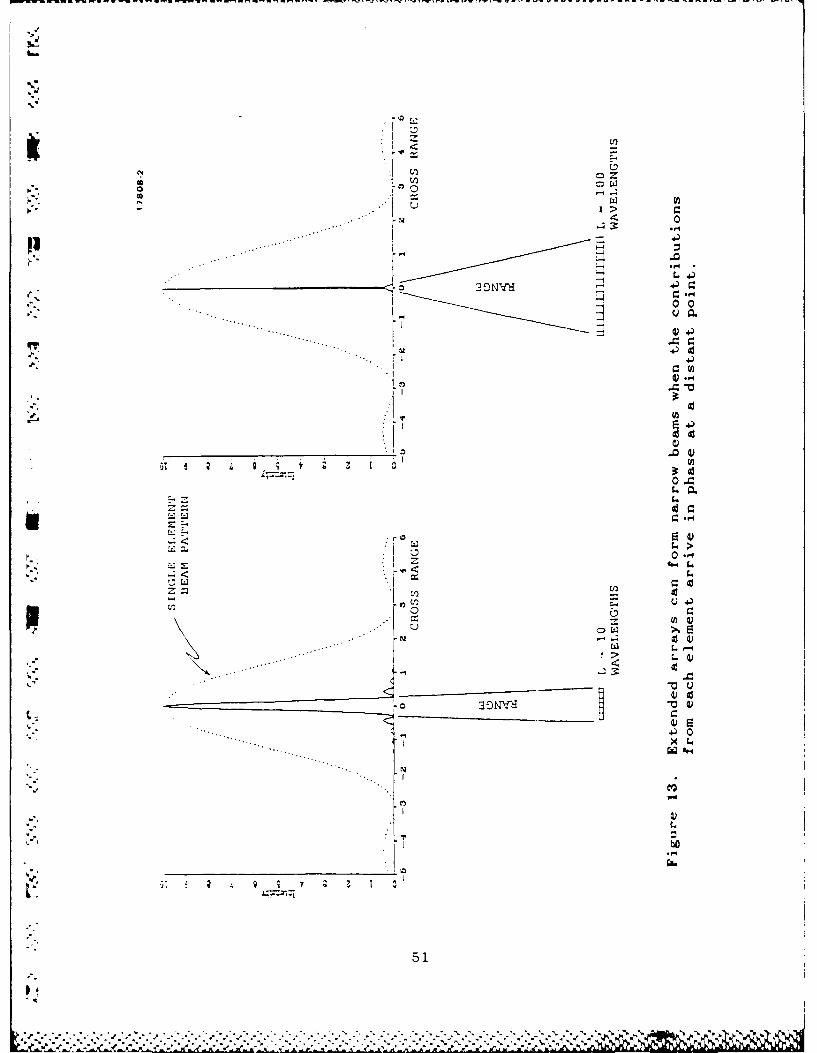
0 0~
0 .4
I.-l
00
4.4)
51

An interesting phenomenon may be seen when the beam is
steered to an off-axis direction. Figures 14(a-e) show the far-
field pattern as the beam is progressively steered to the right.
Beam steering is accomplished by introducing progressive phase
shifts from element to element across the array.
As the beam is steered to the right, the maximum beam
intensity drops and two side lobes appear. The total power in
the beam is shared between the main lobe and the side lobes. The
main-lobe peak intensity closely follows the outline of the beam
pattern from a single element. The side lobes follow somewhat
different curves. The three lobes may be thought of as
diffraction grating orders. The main lobe is the zeroth order.
--,zi The lobe to the right is the +1 order and the lobe to the left
the -1 order. The three lobes steer at different rates. For
S example, Figure 14(c) shows the main lobe steered one division to
the right. The -1 order has moved 1/2 division to the right and
the -1 order has moved 1 1/2 divisions.
Since the main-lobe power falls off with large steering
angles, in radar systems there is usually not much point in
steering beyond the half-power points or about 1 1/2 divisions onthe scale shown here. For a discrimination system, however, the
performance criteria may be considerably different than for a
conventional radar. Half of the power in the beam may be very
adequate to discriminate some targets at the nearer ranges. By
tolerating very high side-lobe levels, a discrimination system
can achieve beam steering over wide angles with about a factor of
four fewer phase shifters in the transmitting antenna than a
search radar.
The envelope of the power curve is determined by the size of
the individual element in the array. Since the cases shown here
0. are for one-wavelength-long elements, the half-power steering
angle corresponds to approximately a 60 ° field of view. If theelement size is reduced to 1/2 wavelength, the half-power field
of view will be extended to nearly 1200, but the cost then
increases from one to four phase shifters per square wavelength
in the antenna.
52
0I
f * ~ . ~ :~c:~:4, ~4~5 5-

oV.
%I
po to -)
........ ........
0 0
r.
4) 0
-)
C
. ........
.... .,." . .
. """ Q )..,
,, ,
.... "..........- --
- t . ; z ; - tE g q
53
4 Lk

-'W ,-W r ri ., i - rl .
%i
1 78086-A
- "(e)
-V............
d. o- t
' I ' I *
-5 -4 -3 -a -1 0 1 2 4
.
Figure 14. Continued.
-0,
54I
a'

The result of trying to phase steer by identically
controlling patches of phase shifters is now clear. A patch of
emitters, all with the same phase, is equivalent to a single
larger element. It will have a proportionally narrower far-field
beam pattern and narrower steering angle before side lobes
become important. Patch phasing is not practical for large-angle
ste-ring. The implication for a discrimination system is that
each phase shifter must be provided with a distinct phase
adjustment signal which is different from its nearest neighbors.
Beam Focus Properties. Most radar systems employ fixed-focus
antennas with the focal distance set at infinity. They radiate
an initially collimated microwave beam which spreads due to
diffraction effects. A typical radar beam width might be on the
order of two degrees due to diffraction spreading.
Due to its very large antenna size, the decoy discrimination
system can produce very narrow beams. The diffraction-limited
beam width to the half-power points is given approximately by X/D
tin radians. For an array diameter D of 10,000 m and a wavelength
X of 3 cm, the main-lobe beam width is approximately 3x1O-6 radians
or 1.7xlO -4 degrees. A larger array can produce a
proportionally smaller beam divergence. This diffraction
spreading angle is considerably smaller than the angle subtended
by the antenna at the target range. As seen from the target at
a distance R of 3x10⁶ m, the antenna subtends an angle of D/R or
3x1O-3 radians, which is 1,000 times greater than the beam
spreading angle. The result is that the large transmitting
antenna can produce a focused spot at range which is about 1,000
times smaller than its own diameter, or about 10 m diameter at
its half-power points.
In order to produce a distant focused beam, the antenna
must launch a converging wave. The wavefronts which leave the
antenna must be aligned to a spherical surface whose center of
curvature is located at the target. At great range, the
curvature is very slight. The amount of phase correction
required to deform a plane wave into the appropriate curved wave
55
I

rW7%n-1 W WnW-W W W WV "W rrW_%r W~r- ~W_ W X-w.-
plane wave into the appropriate curved wave changes very little
between adjacent antenna elements. It may be very feasible to
introduce such small phase corrections as constant shifts to
large-area patches of the array.
Figure 15 illustrates the calculation of patch size for
focusing purposes. A spherical converging wave may be
approximated as a stepped series of flat wavefronts. Suppose x
is the difference between the desired curved wave and a perfectly
flat wave. If the wavefront error x can be kept less than 1/10
wavelength, the degredation in the far-field spot will be
negligible compared to a perfectly smooth curved wave.Degradation of the far-field Strehl ratio scales
approximately as cos2 (x/X) or, in this case, cos 2 (O.l) =
(0.995Y2 - 0.99. From Figure 15, it may be seen that the curved
* wave differs from a plane wave by an amount x for patch sizes
larger than 268 m. This means that, in addition to phase tilts
for beam-steering purposes, the array may be focused by applying
additive uniform phase corrections to relatively large patches of
the array. Focus is very important for the decoy discrimination
system, and it is a fortunate simplification that the corrections
may be applied in a simple additive fashion to large areas of the
array.
Summary. Phased-array beam steering over more than 60* fields of
view is practical for phase-shifter densities of one shifter per
Psquare wavelength in the transmitting aperture. If half-power
beam steering to 120* is desired, then phase shifters must be
spaced at 1/2 wavelength intervals for a density of four phase
shifters per square wavelength. The feasibility of using dense
shifter arrays is primarily an economic issue. If inexpensive
printed circuit designs can be developed, there may be little
cost difference between one and four shifters per square
wavelength. In that case, the denser array will provide superior
performance because of the lower level of side lobes at all
steering angles.
56

-4-)
-Vp *r- 4
-. ~~ 04)
0-4
~. . 'N f-
L, 0
-4)
0 x
O
O
r-4)
w (N
4)
-4 bDr44
*4 0E-
~-4 U I 57
Beam steering requires linear phase tilt adjustments across
the array. In general, each phase shifter will have a different
phase setting than its neighbors, which means that phase
adjustments cannot be applied in patches. This is not to say
that phase adjustments must be continually variable analog
corrections. Phase adjustments may be done in digitized steps as
large as 1/4 wave at each shifter, as is practised in digitally
steered search radars. However, any two adjacent shifters will
require different step settings for some steering angles.
Phasing in uniform patches is not practical.
Beam focus requires only very slight curvatures compared to
plane wavefronts for the antenna sizes and target ranges of
interest in a discrimination system. Spherical waves can be
approximated by stepped plane waves with minimal far-field beam
* degredation if the wavefront error is kept to less than 1/10 of a
-' wave. Relatively large patches can have the same focus
adjustment, which means that separate focus commands are not
required for each phase shifter.
3.4.2 The Effects of Aperture Thinning and Phase Errors on aLarge Phased-Array Antenna
Ideally, the antenna for the ground-based HPM decoy
discrimination system would consist of a nearly circular,
p uniformly filled and uniformly illuminated transmitting aperture.
The purpose of the antenna is to launch a collimated orf converging wave toward a distant target. In an ideal antenna
0 system, the radiated wavefront would be perfectly smooth across
the entire aperture; i.e., all portions of the antenna should be Jperfectly in phase and radiate with equal amplitude. A real
-2 antenna system, of course, will be subject to many compromises,
*. all of which tend to degrade the maximum power density which can
be projected to a target.
58
. 4

It is straightforward to calculate the far-field performance
of a phased array antenna. Conceptually, the field at any
distant point is simply the vector sum of the contributions from
each radiating point at the antenna. In most cases, a large
antenna will be constructed from many identical submodules, which
can greatly simplify the calculational problem. The calculations
presented here are due to R. Kwong, 1985 and 1986. They make
maximum use of antenna sym.metry and computationally efficient
fast Fourier transform algorithms.
The calculations presented below are intended to answer two
questions. First, what is the effect of thinning a phased array
A large array may be typically constructed from smaller modules
which have some dead spaces or do not perfectly join together.
Looking ahead, it is shown below that the amount of power in the
main transmitted beam is reduced approximately by the fill factor
of the phased array. For example, if the transmitting array has
10 percent void space between radiating subapertures, then
approximately 10 percent of all transmitted power will go into
side lobes instead of into the main beam.
The second question considered below is the effect of
antenna phase errors on the peak power at the target. It is
shown that phase errors greater than about X/10 across
significant portions of the antenna begin to seriously degrade
the far-field performance.
Thinned Arrays. Consider the ideal case of a uniformly
illuminated circular transmitting aperture of diameter D, shown
in Figure 16 on top and designated S1 below. The far-field
pattern (Fraunhofer limit) may be calculated in closed form and
is proportional to a Bessel function of the first kind.
The irradiance pattern at a distant target for this well-
known case is the familiar Airy pattern, shown in the lower part
of Figure 16. It consists of a strong central peak surrounded by
several weak bright and dark diffraction rings. The width of the
central peak, i.e., its radius from the maximum to the first
59SC
.-• ,' ''2'. ,-. ... ..... ., . .,e .V

• .
1 7808-2
si Si"'%'2,' 17800-
',.-
--] /
/. I-
. HT. __________ _ _ _ AIRYRAO)
'!
S'4
CENT. OI ZOTA (S IYtD
*! Figure 18. Irradiance pattern for uniformly illuminatedcircular aperture.
.
'.4'
:-F.
60
0.%
-, -%-; ~ ~ *-

I-
zero, is proportional to the range to the target times 1.22 X/D,
as shown in the central-slice intensity plot. The central peak
width also depends upon any focusing properties of the
transmitting antenna.
The power contained within the central peak amounts to 85%
of the total transmitted power. All transmitted power which
Pfalls outside of the main central peak is usually referred to as
side-lobe power. The shape of the peak and position of the
zeroes of the diffraction pattern can be slightly altered by
using nonuniform illumination across the aperture, but for most
practical purposes S1 is the best performance that can be
achieved. The most important feature to note is that large
apertures D and short wavelengths X produce small spots X/D at
the target.
Next compare the baseline performance of S1 to various
thinned arrays. SiC (Figure 17) is a circular aperture with a
large central obscuration. In the case shown, 40% of the
transmitting aperture radius has been removed.
It is well known that a central obstruction can slightly
increase the resolving power of an aperture. The width of the
central or main lobe is clearly seen to be somewhat smaller than
in the S1 case. However, the power in the main lobe is down and
5 the side lobes have increased. In this case, approximately 50%
of the total transmitted power is contained in the slightly
narrower main lobe. The important point to note is that thinning
the aperture has put more transmitted power into the side lobes.
Next consider the array of 64 small circular apertures
designated S64 (Figure 18). The total illuminated area of S64 is
identical to the area of S1. Due to the small spacings between
subapertures, S64 has a slightly larger overall diameter than Si.
For this reason, the main lobe of S64 is slightly narrower than
S1. The peak main-lobe power of S64 is identical to SI, but the
total power in the side lobes is larger. The effect of thinning
61i.

17808-29
sic(0.4 linear obscuration)
sic sic
'"T E
IWNI
.
CET
, s-e
:::1::: F igure 17 . c rclrradiance p e ur.attern for centrally obscured
}c a a
%62

S64 ,,so8.3o
• 00D/8 0000000
g Cl0 0000000
0000000090000 000000000000
• -00000000
0000
17808-31
S64 S64
CENT. HCRIZONTAL (SI AIRY RAD)
Figure 18. Array of 64 small circular subapertures.
63

has been to reduce the width of the main lobe and its total
energy but-not its peak power. Eliminating the circular symmetry
has produced lumpy side lobes with rectangular symmetry in place
of the smooth rings of Si.
The effects of array thinning can be seen more clearly in
the simulations of far-field beam patterns from an array of 16
circular apertures, see Figure 19. With the ratio s/d = 1, the
subapertures just touch each other. The far-field intensity
pattern in Figure 20 shows a single strong main lobe which is
nearly identical to the filled circular-aperture case SI. As the ..
subaperture separation is increased, the main-lobe peak intensity
remAins the same; but the main-lobe width and total power in the
lobe go down. Increased spacing or thinning leads to a larger
fraction of the total power distributed among increasingly strong
side lobes.
The above computer calculations demonstrate a simple scaling
law for thinned arrays. The peak power in the main lobe of a
perfectly phased array is proportional to the total illuminated
area of the array and is independent of the shape or fill factor
of the array. The width of the main lobe, however, is inversely
C178hm.36
CASE SUBAPERTURE PHASE SHIFTS_______(PISTON ONLY)
(D (Do d- A DIFFRACTION-LIMITED
81 = 03 = 0 = 08 =¢9 =011=14-16 = P
® c~j ~ S02 =04 =05 "7 "0O012O13"15 P -
WITH p = X 140C SAME AS B BUT WITH p = k120
D SAME ASBBUT WITH p= X/10
i.,, 19. Array of 16 circular subapertures.
6
r. 64
I:. . . . . . .
.p .-- " . - "•.-.'-;"'."" '"':" " " -v ,-... . .. ;.:..,'. ,:/, ..@ . ,? ' -? ?,.' -,..,

17808.32
s,'d 1EL
9.ZSe
9.75B
SAJg
EL
SdT0.0
-o
6.e.
-V L
4. Sao
SUITELESCOPE AIRY RADIuS
tLA 1.22 Xf/d
Figure 20. Far-field patterns of case A (diffraction-limited).
-. 65
lit %I% -~.
4 p~ .- ~44

power in the main lobe (integral of power over main lobe area) is
a fraction of the total transmitted power and, in fact, is given
simply by the array fill factor:
P (main lobe) = P (filled-array main lobe) x Fill Factor, (15)
For example, if the array is 90% filled, then an additional 10%
of the total transmitted power will be scattered from the main
beam to side lobes. A proof of this scaling law is available in
analytical closed form (see R. Pringle, 1987).
Phase Errors in Arrays. The above calculations of far-field
intensities have assumed that all elements of the array were
radiating with perfectly correct phases. Using the 16-element
square array, it is a straightforward matter to introduce phase
differences between the elements. Figures 21 through 23
illustrate the degradation due to phase errors which alternate
from plus to minus X/N between adjacent subapertures, where
N = 40, 20, and 10, respectively.
It is apparent that phase errors less than * X/20 between
adjacent subapertures are insignificant. Phase errors larger
than ± X/10 cause a significant decrease in the main-lobe peak
power and an increase in the total power scattered to side lobes.
A reasonable design goal for phased-array antennas is to maintain
rms phase errors to less than X/10. For a 3-cm wavelength
corresponding to 10 GHz, the antenna surface figure should be
held either mechanically or electrically accurate to 3 mm.
Summary. Array thinning has no effect on the peak power at the
center of the main beam, but it significantly scatters power into
side lobes. For a given total transmitter power and active
antenna area, the factor by which the total power in the main
beam is reduced is precisely the fill factor of the array.
6
*" 66
I
, .1. .% % % " .% % % - ,%. .- , .% - .. . . . . -% . - . .% " -

17606-33
S/
..
0. 7SO
L
0
-1. .n
4. 7S*
CSO
T
SUITELESCOPE AIRY RADIUIS
1.22 X f/d
Figure 21. Far-field patterns of case B (X/40 piston).
S 67
~ ~ . -*.**.*~**.~ '~*.**.*,*J ...- * - N%

1 7808-34
1. CO
41. 7SO
s/C. 25E
#.Sa
4.s
0.
6.500IT
/ 1.22 C ..
Fiur 22. Far
68
Sr :1'" d !1;& LIU 0.50

A1.. e
1780a1-35
,"-" O.7SO
T
e~e
L
T
4.2S
$.S
.- .. L
1.00
.. -.
LAL
I e. 75.
s/d =3 L
r T
LI-
• SUUTE[LESCOPS AIRY RADIUS
1,22 X1/d
%• '2Figure 23. Far-field patterns of case D (X/IO piston).
"- 69

Spreading out an array of subapertures has the effect of
narrowing the main beam and scattering more power into side
lobes. An HPM discrimination system should probably be designed
for a fill factor approaching 80%. A rectangular close-packed
array of circular apertures, as illustrated above, has a fill
factor of 7/4 = 0.785, which would probably be satisfactory.
Phase errors between subapertures degrade most aspects of a
phased array. Both the peak power in the main beam and the total
power in the main beam are reduced while power in the side lobes
increases. Degradation effects become significant with phase
errors larger than X/10.
3.5 TASKS 17 - 18: HIGH-POWER PHASE-SHIFTER CONCEPT EXPLORATION
"0 3.5.1 Phase-Shifter Arrays
Having established that: 1) beam steering over 60 ° requiris
phase-shifter densities at least as high as one phase shifter per
square wavelength, and that 2) sidelobe suppression requires a
highly filled array, it is clear that a very large number of
phase shifters will be required. Current waveguide phase-shifter
technology is costly and would easily dominate the total system
costs. A simpler and less expensive concept is required. The
following calculations estimate the magnitude of phase shifts
which might be achievable from arrays of simple resonant loops
and dipoles. The results initially look practical and promising.
Consider a resonant LRC loop (Figure 24) as a candidate
phase-shifting element. The loop will couple more or less
strongly to an incident electromagnetic radiation field dependingupon its resonant frequency and its internal losses or Q.
An array or planar sheet of resonant loops (Figure 25) can
be used to retard the phase of a plane wave in transmission. If
the array is placed before a flat reflecting surface, phase
shifts can be obtained in reflection by a double pass through the
array (Figure 26).
70
S.,
-1I

17808-7
RL
Figure 24. Resonant loop.
17808 -8
E 0 PHASE SH IFT
IN TRANSMISSION0
z0
Figure 25. Array of resonant loops.
71

17808-10
INCIDENT PHASE SHIFTEDWAVES REFLECTION
TUNABLE RESONANT LOOPS
L R L R L
C V V7 I
REFLECTING SHEET METAL SURFACE
Figure 28. Phase shift in reflection.
I
The calculation of phase shift versus resonant-loop tuning
will proceed in five steps:
1) Using Faraday's induction law, estimate the voltage induced
in a loop due to an incident plane-wave field.
2) Consider the loop as a nearly resonant harmonic oscillator.
Estimate the steady-state oscillating current induced in the loop
due to the driving voltage calculated in (I) above.
3) Develop an expression for the dipole radiation field from a
loop with a steady-state oscillating current.
6 4) Consider a plane wave incident upon a sheet array of
identical resonant loops. After transmission through the array, Ithe resulting field will be a vector sum of the attenuated
incident field and the field scattered by the array. Compare
this sum field to a time-delayed plane wave, as if it had passed
through a material with some index of refraction and thickness.['S
5) Estimate the number of waves of phase retardation for some
*typical loop dimensions and operating frequencies.
72

Step 1: Faraday's Induction Law. Consider a single-frequency
plane wave incident upon an LRC loop. Rationalized MKS units
will be used throughout these calculations in order to relate the
results to easily measured quantities. In the usual convention,
measurable quantities are taken as the real part of complex
expressions. Consider first a summary of the properties of plane
waves.
Incident fields:
Z If -ZE e i(kz - wt)0
i(kz - wt)"B" 0 : e (17)
kc
For plane waves in free space:
V 3B (18)
x - -S- -at
ikE iwBo 0
: k1B 0 k C E - E 4 E (19)o w1 C 0 00 0
A.
Power flow from Poynting's vector:
S Ex H E i (20)
73
C

-2 2(1
average 2 E 0 ° 0 2#E 2o)
Next consider the voltage induced in a loop due to a time-
varying magnetic field aligned normal to the plane of the loop,
given by Faraday's induction law. Since a small loop antenna
couples to the magnetic field rather than to the electric field,
it is convenient to perform most of the following calculations
with the magnetic components of the electromagnetic wave. The
induced loop voltage (Figure 27) will serve as the driving
voltage for oscillating currents in the loop.
Induced Voltage:
VDrive = dl (22T
d B s
dtdt Loop
iwA B eiwtLoop o
"ILet V D e itthen VD =I w A B (3Drive DDLoop o023
Step 2: Driven Harmonic Oscillations. An LRC series loop may be
modeled by a linear differential equation which is derived from
Kirchhoff's voltage law around the loop (Figure 28):
Drv L% ~ dI dVr c' V L IC C (24)Drve L VR * V L d- C dt
74
[ -d
6,

17808-11
p
IR
ICAREA, AL P
Figure 27. Loop in B-field.
1 7808 -12
Figure 28. Voltage-driven loop.
~~75
9999~*9 ~ .- il IA9.

VDrive L - + IR + I dt
Drive dDr ive =L -R I + 0 I
%I
Assume:
VDrive = Deiwt (VD complex) (25)
I 1 0oe (I° complex) (26)' IForced loop oscillations:
-iWVD -w2 LI o iwR + (27)
iw - 2l1
iwvD (w2 L I) I[ iwRID o
WV D V D
o 1 1 2 1(w L - 0 ) iw R R- -- (w L- )
5-w
7 VD 21
R iL ( 2 1 o LCw EC
* vD
iL 2 2. (28)R -(w2 -w 2
Uj 0w76
76
I
•5']%. ,A

.1m
The steady-state loop current depends upon the magnitude of the
driving voltage, the loop resistance or Q factor, and the
detuning from resonance.
Step 3: Fields Radiated by an Oscillating Current Loop. The
magnitude of the magnetic moment I of the loop (Figure 29) is
given by
"'" -i~t
A Loop I A Loop oe (29)
17808-13
Px
z DIPOLEZ RADIATION
Y
m MAGNETIC MOMENT LOOP LIES IN THE X-Z PLANE
Figure 29. Magnetic moment of loop.
77

dd
i ~ ~~From PanofskY &-) Phillips, first edition Eq. (13-69) , or second
iAok 2 eikR
B(R) - R 1 x (; x R)] (30)47r R3
Consider the magnetic field of the scattered dipole radiation
(Figure 30):
ik 2 ikR (I~o -iwt
scattered max 47r R Loop o
17808-14
DIPOLE
SCATTERING RESONANT
INCIDENT LOOPB FIELD,
Figure 30. Scattered dipole field.
78
0

I-..
in the Y-Z plane (plane of the drawing),
% ipo w A Loop Ii (kr -wt)B&(r,t) =2 cLr2 o cos8 e (32)
Step 4: Index of Refraction of an Array of Resonant Loops.
Consider a sheet of magnetic dipoles (Figure 31) which are driven
in-phase by an incident wave. We want to calculate the field due
to the sheet at point P.
Far from the sheet, cos 0 1 1. The field at P may be found by
summing the contributions from all of the dipoles. Each ring(Figure 32) contributes (2rpdp)NA dipoles, where NA = the number
of dipoles/unit area.
The total field due to the sheet of dipoles:
B(z) NA B(r,t) 2wp dp (33)
Dipole jSheet o
,j We change the integration variable:
,2 p2 2. .r -- + z ,
6 2r dr 2p dp then
e 2r dr (34)Dipole 4w c rSheet z
2i NA w A I# 2Lo e i(kr-wt)dr
2c 2
z
79
-- F
-" " " " . ., ." .""," 4. ' ," ", ".. " € ', ? " "', " .% Q . :' 'v 'o:, ' ', " . . . .

17808-15
0
0
00
° V.,e i(k z _w t ) 4
Y Bo<>o 0,
i~i B (r, t)
40IFigure 31. Sheet of magnetic dipoles.
17808-16
dp
1
Figure 32. A ring of dipoles.
80
- 1

B(z) 2N/s AOORl 0 -i wt feC dr
Dipole 2c2
Sheet
2c
Here, N I e =0 ,because N *0 and 1 - 0 for p 4oo in anyA Ao A 0
real physical system. Thus,
B(z) - AL P 0 e i~ z - w )(35)
Dipole 2c
Sheet
Now put in I. and compare to the expression for the incident B
field. From Eq. (28),
NA'u 0 Loo VD i(kz -wt)
B(z) -L 2 2 e . (36)Dipole 2c [R + i W 0w -
SheetW 0
Using VD from Eq. (23),
N N/w AL iw B ABz_ A 0 Loo o Loop ei(kz w Ct)
Dipole 2c 'R i L (w~ 2 w2
Sheet 0
81
dI a

iN 2 A 2
9(z) Ao Loop B ei(kz - wt) (37)y-L 2 w2 j 0Dipole 2c [R + i (W -WSheet
0
Note the phase shift i with respect to the incident wave,
= y B ei(kz - wt).
Now estimate the index of refraction. Suppose the incident wave
had passed not through a scattering dipole sheet (Figure 33), but
through a material with index of refraction n and thickness Az
(Figure 34).
Inside the material, the wave velocity v = c/n. The additional
time required to pass through the material is
At = (n- 1) Azc
Thus, after passing through the material,
i[kz + (n - 1)w Az - wt]B after B o e
Set this expression = transmitted - scattered fields:
B' (kz - wt) iw(n - 1)Az/c B ewt)
eB(z) e i(kz - wt) (38)o Dipoleo
Transmitted SheetWave
a,.
, 82

SCATTERING 17808-17
, - DIPOLES
INCIDENTWAVE -
TRANSMITTED SCATTERED, WAVE WAVE
Figure 33. Scattering by dipole sheet.
4
17808-18
4,
A
Figure 34. Delay by dielectric layer.
j &8
-5 83
4q..

Note a simplifying assumption: Assume that the incident
wave is transmitted by the dipole sheet without loss and that it
adds coherently to the wave scattered from the dipole array:
B0 = B.. This assumption will be approximately correct when the
scattered wave amplitude is small compared to the incident wave.
This approach assumes that the dipole sheet will make only a
small change to the transmitted wave, which would be the case for
* a sufficiently thinned array of dipoles. An exact expression
without this assumption requires an iterative solution. For
n :1 , we can simplify Befter. This approximation also assumes
that the dipole sheet has only a small effect on the transmitted
wave. Thus,
iw(n - 1)Az/cn Az
e 1 - iw(n - 1)- Ic
iIl - iw(n - 1)] B e i(kz wt) B e(kz wt) + B(z)- 0 0 Dipole
Sheet
iNA 2 A2
iw(n - 1)A-z B ei(kZ - wt) A o Loop B ei(kz - wt)c 2c [R iL (W 2 2 0
wj 0
N 2 2
w(n - 1) AZ A/OW Lc c L 2 2
W 0
A20. NA A4ot L02
. n - -(39)Az 2 R L ( 2 _ 29
V 84
S o
O-

Remember that NA is the number of dipoles per unit area, an
area density. The change in index of refraction can also be
related to a volume density of dipoles, NV , by the simple
relation
NA/Az = NV Thus,
I A2
n- Nv °W A Loop (40)L 22 [R + i- (Cw
0 The change in microwave index of refraction depends upon theA,
volume density of scattering dipoles in exactly the same way that
an optical index depends upon the density of atoms in a solid.
VNote that, for frequencies off resonance, the expression is acomplex number, which indicates absorption effects.
Step 5: Estimating the Number of Waves of Phase Shift. Now
consider some practical numbers for the phase shift. We would
like to achieve a phase shift of up to 2w radians, which is
equivalent to a path length change of one wavelength:
(n - 1)Az = X.
From Eq. (39),
NA A2
A " 1o w Loop(n - )Az (41)
- = 2 [R + L (- 2 _ 2 )]w o
85
,.. 4
:0

The largest effect occurs on resonance, w0 = w. Assume that
010 - 1 1 - 2 {•]
f = 10 GHz , w = 2 x 10 si = 3 cm 3 x 10m -1
A =1cm2 = -4 m 2
Loop
and suppose that the loops are 1 cm square and spaced on 2/3 X =
2 cm spacings (Figure 35). This results in
-2 3 -2NA = 50 x 50 m 2.5 x 10 mith
o 41r x 1O-7 V s/A m and
R =1 0 =1 V/A (effectively a dielectric loss in C),
(n-1)Az 2.5 x 10³m-2x 4w x 10-7V s A-1m - lx 2w x 100s-lx (1 -4M 2 2
2 x 1 V/A I
m
17808-20
2 cm
F ~DD
Figure 35. Resonant loop dimensions. --
86
I 7.-1

[,'
This result is large compared t- one Navelength. We may
conclude that the above assumptions that the dipole sheet will
scatter only a small portion of the incident wave are incorrect.
A more accurate estimate might be obtained by eliminating these
it small scattering approximations, but additional fact.ors should
• ., also be included. For example, this calculation has neglected
the effects of mutual coupling between adjacent resonant loops.
We conclude that a sheet of resonant loops can very strongly
perturb the phase of an incident wave. A practical system may be
able to use loops significantly smaller than those assumed above.
3.5.2 Magnetic Field Antennas
At frequencies above 1 GHz, the single-turn LRC resonator
begins to resemble a wedding ring with a slot cut through it
P . (Figure 36). In the limit of very small C, the loop approximates
a dipole antenna. If the loop is straightened, the structure
reduces to a simple half-wave dipole.
.1 17808-21
I
C8 >
Figure 38. Single-turn resonator.
87
I%

From this simple picture, it can be seen that the loop
should have a circumference smaller than X/2. As L is madeNsmaller, C can be made larger for any given resonant frequency.
Typically, ohmic and radiation losses in L are larger than
dielectric losses in C. Thus, a reduction in L leads to a
* resonator with higher Q factor and a sharper resonance. The
reduced area of the loop also couples less strongly to the
surrounding electromagnetic fields, which may or may not be an
* advantage.
In principle, the inductance of a single-turn loop may be
calculated from first principles. In practise, the result is a
sensitive function of the diameter of the wire and the
distribution of currents on the surface and within the volume of
the wire.
The inductance of a small single loop can be determined by
direct measurement (Radio Amateur's Handbook, 1979, p. 2-11).
Consider a single-turn loop constructed of No. 12 bare wire
(2.05 mm diameter) with a pitch of 8 turns per inch ( a non-
planar loop) and an inside diameter of 1/2 inch (1.27 cm). The
measured inductance is 4.5 x 10⁻⁸ H. At a frequency of 10 GHz,
this inductance could resonate with a capacitor of 5.6 x 10⁻³ pF,
which is probably too small to be practical. Note also that the
inside circumference of the loop is 3.99 cm, which is
significantly longer than half of the 3-cm wavelength.
For a 1O-GHz phase shifter, the loop must be smaller than 40.47 centimeter diameter to meet the X/2 criterion, which could
be inconveniently small. However, there is another construction
epossibility. Dipole antennas are known to radiate well at their
third harmonic frequencies, i.e., when their length is 3X/2.
Resonant-loop antennas share this property.
4 In the older radio amateur literature, capacitively tuned
resonant-loop antennas are known as VHF halo antennas
(Figure 37), (Radio Amateur's Handbook, 1963, pp. 492-4). The
resonant loop may be designed for a frequency of 1/3 of the
j
88
'

,4. *4~
4. ~.
V.
M.~ ~
.s,*, ~-*
-'p
~*.1 ,*
* 17808.23
% p.-V....
Pr%.
p1.
0
Ip..
"p.
Figure 37. The 2-band halo antenna set up for 50-MHzoperation; changing to 144 MHz involvesdecreasing the plate spacing and resettingthe matching clip and series capacitor.
'p..,. ~:
0.*4-. .~
p-I.
~4LP
p...
-I.. ~
89
04 I
P * SWWf4~P - ---~. - -~ . - -'~ P4. 7 '~ *~VV ~

desired operating frequency. The circumference of the ioop is
typically about X/3 at the longer wavelength. A single capacitor
can tune the resonance at either the fundamental or the third
*' harmonic frequency.
A third-harmonic design for 10 GHz (X 3 cm) would have the
following dimensions:
Loop diameter d = 1 cm.
Loop circumference = 3.14 cm
(approximately X/3 at the longer 9-cm wavelength).
Estimated inductance: L ; 2.8 x 10⁻⁸ H
Capacitance required to resonate at 3.3 GHz:
C z 8.14 x I0-1 F.
For a parallel-plate capacitor with plate spacing small compared
to the plate diameter, the capacitance is given approximately by
C = E0A/d, with E0 8.83 x 10⁻¹² F/r. An air-spaced capacitor
with square plates 1mm on a side and spaced by 0.1 mm has a
capacitance of approximately 8.84 x 0-1 F, which is just about
right. Thus, a third-harmonic phase-shifter array might consist
of 1-cm loops made from 1-mm diameter wire with a capacitor gap
spacing of 0.1 mm.
3.5.3 Electric Field Antennas
As observed above, a resonant-loop antenna coup,predominately to the magnetic field of an inciden-
electromagnetic wave. A straight half-wave ,
A couples to the electric field. An array of .
similarly used to shift the phase of an
transmission or reflection (Figure 38
.o
&
4 mmm m
AS@

A189 311 GROUND BSED H1014 PONER MICROWAVE DECOY DISCRIMINATION 212
SYSTEM(U) HUGH4ES RESEARCH LABS MALIBU CAW 0 ECKHARDT ET AL 23 DEC B? NAC-REF-GO656
UMCLASSIFIED N888i4-86-C-8878 F/G 19/12 UL

1112.2
MICROCOPY RESOLUIONTETCHR
NAIOALBUEA F TAOAOSNL-
17 1110
1.
111_2
MIRCP RSLTO TS HR

17808-25
V2/
I I I I
REFLECTING SURFACE I I
TRANSMISSION REFLECTIONPHASE SHI FTER PHASE SHIFTER
Figure 38. Dipole phase-shifter arrays.
In reflection, quarter-wave antenna elements may be deployed
against a reflecting ground plane. Note that, at a conducting
surface, the local electric field must be normal to the surface
which is precisely optimal for coupling to these dipole arrays.
A reflecting ground plane may be particularly convenient, since
all control wires can be hidden behind the ground plane where
they will not scatter the incident fields.
To achieve a variable phase shift, some method of tuning the
dipoles through resonance must be found (Figure 39). It might
consist of either capacitive or inductive loading at the center
of the dipoles. Alternately, it may be feasible to digitally
switch dipoles of various lengths to achieve above, at, or below
resonance conditions.
p.9
91

17808-26
Figure 39. Dipole tuning methods.
In the magnetic antenna case, it is straightforward to
adjust the Q or sharpness of the resonance by changing the ratio
of L to C. In general, heavily loaded antennas which are
resonant but much smaller than the wavelength tend to have sharp
resonances. Dipole antennas can be loaded with inductors and
will exhibit similarly sharp resonances, but inductive loading is
generally impractical at high frequencies. Some combination of
switched stub tuning may provide both reasonably sharp resonances
and convenient digital switching (Figure 40).
17808-27
DIGITALLY SWITCHED REFLECTINGARRAYS
E-FIELD COUPLING B-FIELD COUPLING
Figure 40. Digitally switched reflecting arrays.
92

SECTION 4
*CONCLUSIONS
The effort this year has again resulted in a considerably
increased understanding of the critical issues affecting the
feasibility of the proposed ground-based HPM decoy discrimination
system. We have shown that the predicted damage mechanism can be
produced in high vacuum, and that the experiments agree with the
predictions of our HPM/target interaction model. We have
proposed a mechanism that might enable the production of
measurable thrust reactions from decoys with much thicker metal
coatings than what was previously thought to be feasible. We
have established bounds on some important parameters of the
antenna system, and potential solutions to the single most
critical problem - the cost of the large phased-array antenna -
2i have been identified.
Thus, the emphasis during the next year of performance will
be on the theoretical and experimental study of HPM interactions
with thick metal coatings and on feasibility demonstrations of
the proposed phase-shifter approach.
ft.
93

N
REFERENCES
1. D.O. Stringfellow, Calspan Secret Working Paper, 8th April,1986, Doc. Control Log #0945961.
2. "CRO Handbook of Chemistry and Physics" 49th ed. ChemicalRubber Co., Ohio, 1969, p. D-33.
3. C. Kittel, "Introduction to Solid State Physics" Wiley &Sons, 1953, p. 130.
4. Ref. (2), p. E-10.
5. Ref. (3), p. 150.
6. "Machine Design", Vol. 59, No. 8, 150, (April, 1987).
7. M. Born & E. Wolf, "Principles of Optics" Pitman Press 1970.
8. J. Ready "Effects of High-Power Laser Radiation" Ac. Press(1971) p 107.
9. A. McDonald "Microwave Breakdown in Gases", Wiley & Sons,1966, p. 69.
10. "Relation between the RF discharge parameters and plasmaetch rates, selectivity and anisotropy", C.B. Zarowin, J.Vac. Sci. Technol. A2 1537 (1984).
11. "A theory of plasma-assisted chemical vapor transportprocesses", C.B. Zarowin, J. Appl. Phys. 57 929 (1985).
12. "Frequency effects in plasma etching", Daniel L. Flamm,J. Vac. Sci. Technol. A4 729 (1986).
13. "Plastic Insulating Materials", R.N. Sampson, in StandardHandbook for Electrical Engineers, D.G. Fink andJ.M. Carroll, eds., Table 4-64 (McGraw-Hill, New York,1968).
14. "Secondary Electron Emission", P.E. Best in Encyclopedia ofPhysics, R.G. Lerner and G.L. Trigg, eds., (Addison-Wesley,Reading, Massachusetts, 1981) p. 904.
015. "Electron and Ion Impact Phenomena", Edward W. Thomas ibid.
p. 240.
L
A 95
0

16. "Ground-Based High-Power Microwave Decoy DiscriminationSystem", Wilfried 0. Eckhardt, Frank Chilton andJames G. Small, Hughes Technical Summary, Report No. 1,Contract N00014-86-C-0878.
17. H. Brandt, A. Bromborsky, H. Burns, and R. Kens, "MicrowaveGeneration in the Reflex Triode," Proc. 2nd Int. topicalconf. on High-Power Electron and Ion-Beam Research andTechnology, Cornell University, Ithaca, New York, 649(1977).
18. M. Read, R. Seeley and W. Manheimer, IEEE Trans. Plasma
Sci., PS-13, 398 (1985).
19. L. Ives, M. Caplan, H. Huey, "High Pulsed Power MicrowaveSource Studies", Proc., 3rd Natl. Conf. on High PowerMicrowave Technology for Defense Applications, Albuquerque,NM, Dec. (1986).
20. J. Clark, T. Orzechowski and S. Yarema, "An Efficient High* Power Microwave Source at 35 GHz Using an Induction Linac
Free Electron Accelerator", Proc., 3rd Natl. Conf. on HighPower Microwave Technology for Defense Applictaions,Albuquerque, NM, Dec. (1986).
S .
96
q (

*4 0- 0 0 0 0 0 S 0 S S S S