DOI: 10.1007/s00339-006-3811-x Appl. Phys. A 87, 17–22 (2007) Rapid communication Materials Science & Processing Applied Physics A a. klini 1 a. mourka 1,2 v. dinca 1,3 c. fotakis 1,2 f. claeyssens 1,4, ✉ ZnO nanorod micropatterning via laser-induced forward transfer 1 Institute of Electronic Structure and Laser (IESL), Foundation for Research and Technology – Hellas (FORTH), P.O. Box 1527, Heraklion 71110, Crete, Greece 2 Physics Department, University of Crete, Heraklion 71409, Crete, Greece 3 National Institute for Lasers, Plasma and Radiation Physics (NILPRP), Lasers Department, ‘Optical Processing of Advanced Materials’ Group, 409 Atomistilor Street, P.O. Box MG-16 Magurele, 077125 Bucharest, Romania 4 School of Chemistry, University of Bristol, Bristol, BS8 1TS, UK Received: 12 September 2006/Accepted: 28 November 2006 Published online: 19 January 2007 • © Springer-Verlag 2007 ABSTRACT We report a method for micropatterning (25–900 µ m 2 pixel size) of ZnO nanorods onto a silicon substrate via a low-temperature (overall under 100 ◦ C) two-step process, involving a laser-based direct-write technique (laser-induced for- ward transfer) and sequential chemical growth. The rods produced via this route are aligned in the [0001] crystal direction. Photoluminescence shows, next to the band- gap emission, strong green-yellow emission centred at ∼ 570 nm. Additionally, the rod arrays show excellent field-emission properties with a threshold field for emission of 5V/µ m. PACS 61.82.Rx; 81.10.Dn; 81.16.Mk 1 Introduction Zinc oxide is a promising candidate material for the next-genera- tion electronic and photonic devices. Its large band gap (3.3 eV) together with its large exciton binding energy makes it an interesting candidate material for solid- state lasers [1]. It can be readily doped with Ga or Al, to produce transpar- ent and conducting oxide coatings [2], and doping with Co results in a diluted magnetic semiconductor which can be incorporated in spintronic devices [3]. Additionally, the biocompatibility of ZnO makes it an important candidate to interface devices with biology [4]. A striking feature of ZnO is its tendency to form aligned nanorods under specific conditions; this behaviour is observed in vapour–liquid–solid (VLS) growth [5], pulsed laser deposition (PLD) [6], epi- taxial electrodeposition [7] and aqueous ✉ Fax: +44-117-925-1295, E-mail: [email protected] chemical growth (ACG) [8]. The solu- tion growth method has several advan- tages: (i) it can be easily scaled up, (ii) it is environmentally friendly and (iii) it is a low-temperature synthesis route for these one-dimensional ZnO structures. Integration of ZnO nanorods within devices and applications necessitates the development of positioning tech- niques. Recently, two different pattern- ing strategies have been adopted: (i) post-growth immobilisation and (ii) pat- terning via surface pre-treatment. An example of post-growth positioning of nanorods is given in the study of Huang et al. [9]. In this study complex three- dimensional patterns of horizontally aligned nanorods are assembled via combining microfluidic channels with nanopatterning of surfaces. A second approach is pre-treating the surface with zinc [10] or zinc acetate [11] to yield a precursor pattern, which can be used for further chemical deposition of ZnO rods. For example, Lee et al. [12] em- ployed microfluidic channels to write micro- and nanometre patterns of zinc acetate precursor and successfully grew vertically aligned ZnO micropatterns of these pre-patterned substrates. In this study we report the growth of ZnO nanorod micrometre patterns via a two- step process, pre-patterning of a zinc precursor layer via a direct-write tech- nique, and sequential chemical growth of ZnO nanorods. 2 Experimental To fabricate the zinc precur- sor patterns the laser-induced forward transfer (LIFT) microdeposition tech- nique was used. In LIFT, a pulsed laser beam is focused on a thin film of transfer material through a transparent support. Under laser irradiation, a micrometre- size droplet of the film material is ejected and transported to a receptor surface. With this technique a customer- defined pattern can be printed via se- quential transfer from a target to a re- ceiver surface. The target surfaces were quartz wafers with as transfer mate- rial 40-nm thin films of zinc, obtained via sputtering, and Si(100) pieces were used as the receiver surface. The dis- tance between the target and the receiver surface was set at 100 µ m. The target– receiver pair was placed in a minia- ture vacuum chamber pumped to the pressure of 10 −2 mbar using a rotary pump. This vacuum chamber is posi-

Welcome message from author
This document is posted to help you gain knowledge. Please leave a comment to let me know what you think about it! Share it to your friends and learn new things together.
Transcript
DOI: 10.1007/s00339-006-3811-x
Appl. Phys. A 87, 17–22 (2007)
Rap
idco
mm
unic
atio
nMaterials Science & ProcessingApplied Physics A
a. klini1
a. mourka1,2
v. dinca1,3
c. fotakis1,2
f. claeyssens1,4,�
ZnO nanorod micropatterningvia laser-induced forward transfer1 Institute of Electronic Structure and Laser (IESL), Foundation for Research and Technology –
Hellas (FORTH), P.O. Box 1527, Heraklion 71110, Crete, Greece2 Physics Department, University of Crete, Heraklion 71409, Crete, Greece3 National Institute for Lasers, Plasma and Radiation Physics (NILPRP), Lasers Department,
‘Optical Processing of Advanced Materials’ Group, 409 Atomistilor Street,P.O. Box MG-16 Magurele, 077125 Bucharest, Romania
4 School of Chemistry, University of Bristol, Bristol, BS8 1TS, UK
Received: 12 September 2006/Accepted: 28 November 2006Published online: 19 January 2007 • © Springer-Verlag 2007
ABSTRACT We report a method for micropatterning (25–900 µm2 pixel size) ofZnO nanorods onto a silicon substrate via a low-temperature (overall under 100 ◦C)two-step process, involving a laser-based direct-write technique (laser-induced for-ward transfer) and sequential chemical growth. The rods produced via this route arealigned in the [0001] crystal direction. Photoluminescence shows, next to the band-gap emission, strong green-yellow emission centred at ∼ 570 nm. Additionally, the rodarrays show excellent field-emission properties with a threshold field for emission of5 V/µm.
PACS 61.82.Rx; 81.10.Dn; 81.16.Mk
1 Introduction
Zinc oxide is a promisingcandidate material for the next-genera-tion electronic and photonic devices. Itslarge band gap (3.3 eV) together with itslarge exciton binding energy makes it aninteresting candidate material for solid-state lasers [1]. It can be readily dopedwith Ga or Al, to produce transpar-ent and conducting oxide coatings [2],and doping with Co results in a dilutedmagnetic semiconductor which can beincorporated in spintronic devices [3].Additionally, the biocompatibility ofZnO makes it an important candidateto interface devices with biology [4].A striking feature of ZnO is its tendencyto form aligned nanorods under specificconditions; this behaviour is observed invapour–liquid–solid (VLS) growth [5],pulsed laser deposition (PLD) [6], epi-taxial electrodeposition [7] and aqueous
� Fax: +44-117-925-1295, E-mail: [email protected]
chemical growth (ACG) [8]. The solu-tion growth method has several advan-tages: (i) it can be easily scaled up, (ii)it is environmentally friendly and (iii) itis a low-temperature synthesis route forthese one-dimensional ZnO structures.
Integration of ZnO nanorods withindevices and applications necessitatesthe development of positioning tech-niques. Recently, two different pattern-ing strategies have been adopted: (i)post-growth immobilisation and (ii) pat-terning via surface pre-treatment. Anexample of post-growth positioning ofnanorods is given in the study of Huanget al. [9]. In this study complex three-dimensional patterns of horizontallyaligned nanorods are assembled viacombining microfluidic channels withnanopatterning of surfaces. A secondapproach is pre-treating the surface withzinc [10] or zinc acetate [11] to yielda precursor pattern, which can be used
for further chemical deposition of ZnOrods. For example, Lee et al. [12] em-ployed microfluidic channels to writemicro- and nanometre patterns of zincacetate precursor and successfully grewvertically aligned ZnO micropatterns ofthese pre-patterned substrates. In thisstudy we report the growth of ZnOnanorod micrometre patterns via a two-step process, pre-patterning of a zincprecursor layer via a direct-write tech-nique, and sequential chemical growthof ZnO nanorods.
2 Experimental
To fabricate the zinc precur-sor patterns the laser-induced forwardtransfer (LIFT) microdeposition tech-nique was used. In LIFT, a pulsed laserbeam is focused on a thin film of transfermaterial through a transparent support.Under laser irradiation, a micrometre-size droplet of the film material isejected and transported to a receptorsurface. With this technique a customer-defined pattern can be printed via se-quential transfer from a target to a re-ceiver surface. The target surfaces werequartz wafers with as transfer mate-rial 40-nm thin films of zinc, obtainedvia sputtering, and Si(100) pieces wereused as the receiver surface. The dis-tance between the target and the receiversurface was set at 100 µm. The target–receiver pair was placed in a minia-ture vacuum chamber pumped to thepressure of 10−2 mbar using a rotarypump. This vacuum chamber is posi-
18 Applied Physics A – Materials Science & Processing
tioned on a computer-controlled x–ytranslation stage, allowing a maximum25×25 mm2 movement with a 1.25-µmpositioning resolution. A distributed-feedback dye-laser-based femtosecondexcimer laser (λ = 248 nm and τFWHM =450 fs) was used as a laser source forthese experiments [13]. The laser beamwas focused onto the target surfacethrough an image-projection microma-chining system and the laser spot sizewas varied between 5 × 5 and 30 ×
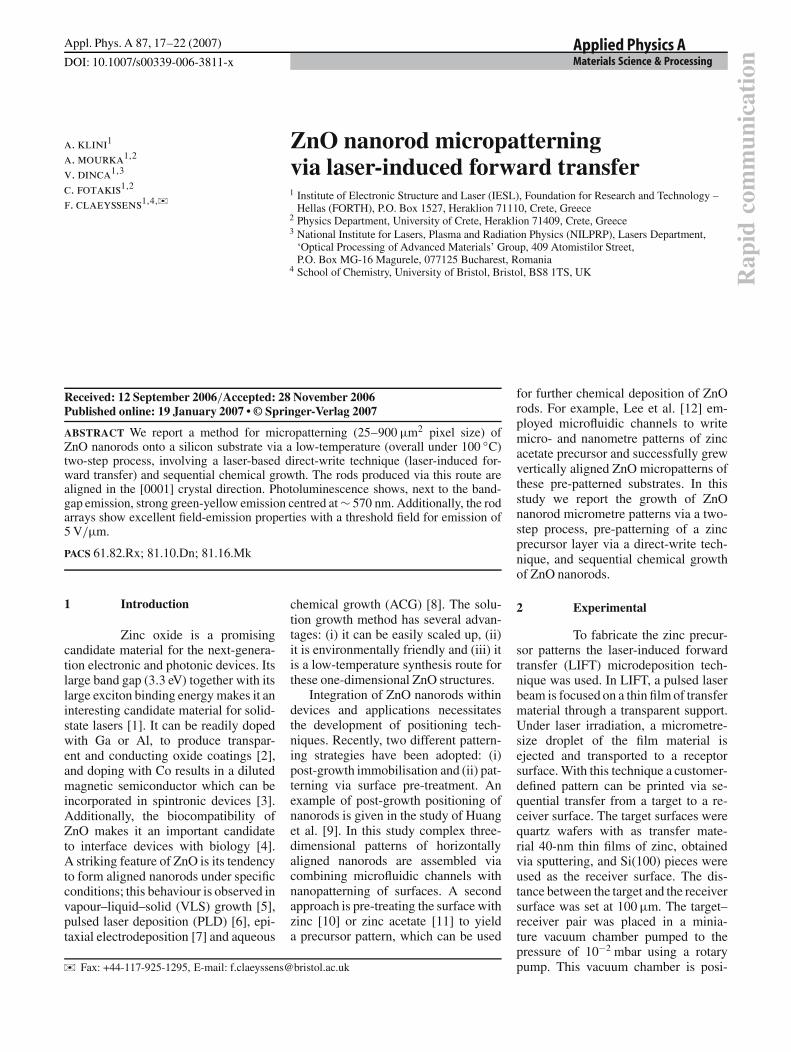
FIGURE 1 SEM figure of a denserectangular array of ZnO nanorods.The pattern consists of a 9× 10 ar-ray of ZnO nanorods. (a) shows thepattern and (b) and (c) show de-tails of the indicated regions. (d)shows a pre-growth Zn pattern, theinset shows the input pattern fromthe computer-controlled LIFT pro-cess and (e) depicts a detail of (d).The scale bars are 10 µm for (a),1 µm for (b), (c) and (e) and 100 µmfor (d)
30 µm2. The average incident fluencewas kept at 170 mJ cm−2. During thedeposition process the target area wasviewed through a CCD camera. A moredetailed description of the experimen-tal LIFT set-up has been given else-where [13].
Following LIFT deposition the Znpatterned substrates were chemicallytreated to synthesise ZnO nanostruc-ture arrays [10]. The reactive solu-tion was 80 mL of 0.02 M aqueous
solution of zinc nitrate hexahydrate(Zn(NO3)2(H2O)6, Riedel-de-Haen,98%) and 2.5 mL of ammonium hydrox-ide (28 wt % NH3 in water, Fluka, 99%).The Zn patterned substrates were im-mersed in the solution for 6 h and main-tained at the temperature of 90 ◦C im-mediately after mixing. The as-grownsamples were rinsed in acetone solu-tion and placed in an ultrasonic bathfor 10 min. The morphology of the de-posited samples was examined by scan-

KLINI et al. ZnO nanorod micropatterning via laser-induced forward transfer 19
ning electron microscopy (SEM). Thecrystallinity was investigated throughX-ray diffraction (XRD) at θ/2θ con-figuration. Room-temperature photolu-minescence (PL) was measured usinga He-Cd laser (λ = 325 nm). The field-emission properties of the ZnO nanorods,as grown on Zn substrates, were meas-ured using a two-parallel-plate config-uration in a high-vacuum chamber atroom temperature [14]. The distancebetween the ZnO nanorods and the an-ode was set at 150 µm. A voltage witha sweep step of 100 V was applied be-tween the anode and the cathode to ex-tract the electrons from the nanorods.The emission current was measuredusing a Keithley 617 electrometer.
3 Results and discussion
In Fig. 1 typical SEM imagesof the ZnO nanorod arrays are shown;more examples of arrays prepared withdifferent Zn precursor dimensions andpatterns are given in the appendix. InFig. 1a an overall view of a dense 9 ×10 array of 20-µm spots (or pixels)with a distance of 1 µm between themis given. Figure 1b and c show detailsof regions outside and within the ar-ray, respectively. In both Fig. 1a andc the pixel pattern with the 1-µm sep-aration distance is clearly observable.Within the pixels the initial Zn depositis covered by dense well-aligned ZnOnanorods having diameter and length of100 nm and 1.5 µm, respectively, in ac-cordance with the nanorod parametersgiven in [10], for growth under similarexperimental conditions. The SEM pic-tures indicate that the chemically grownvertically aligned ZnO nanorods areconfined to the regions where the zincprecursor pattern was directly writtenon the silicon substrate. At the bordersof the pattern, this vertical alignmentceases to exist and the rods grow atoblique angles with the silicon-substratesurface. Outside the pattern (Fig. 1b)there is a noticeable density of more ran-dom, flower-like structures, the densityof which decreases with increasing dis-tance from the pattern. These observa-tions can be rationalised by consider-ing the LIFT process. Under the givenconditions, LIFT produces a highlyforward-oriented plume, mainly con-sisting of small particles and gases (seealso [15]). Indeed, SEM images of the
deposited Zn pattern before chemicalgrowth reveal a dense particulate de-posit after LIFT (Fig. 1d and e). Fig-ure 1d shows a line pattern (the inputfor the computer-controlled LIFT pro-cess is given in the inset) deposited viaLIFT and Fig. 1e depicts a detail ofthis pattern. Although the overwhelm-ing majority of the material is forwardtransferred, a small amount of materialwill travel at an angle with the targetsurface normal. Consequentially, someparticles will deposit outside the de-position spot boundary (seen as whitespecks in Fig. 1d), which will also trans-late to a depletion of particle densityat the boundary itself. The Zn par-ticles convert to ZnO during the initialstages of chemical growth [10], produc-
FIGURE 2 XRD spectrum of the as-grown ZnO arrays on Si. The ZnO diffraction peaks are assignedfollowing the index of the diffracting surfaces; the peaks assigned as * are diffractions from the Sisurface
FIGURE 3 Wavelength-dispersed PL spectrum of the as-grown ZnO arrays on Si. The photolumines-cence was performed using a He-Cd laser (λ = 325 nm)
ing a well-aligned ZnO precursor film(in the [0001] crystal direction) in thepattern centre, but poorly aligned ZnOparticles at the pattern boundary andoutside the pattern. The lateral spreadof the particles in the LIFT ablationplume also indicates a lower boundaryof pattern dimensions that can be writ-ten. This lower boundary, inferred fromthe patterns that were written (see alsoappendix), is 5 × 5 µm2. LIFT print-ing patterns can be further improvedvia tuning the acceptor–receiver dis-tance and the laser parameters (pulseduration and fluence); for example, pat-terns of micrometre metal droplets havebeen produced by using a nanosec-ond Nd:YAG laser at 1064 nm slightlyabove the melting threshold of the metal
20 Applied Physics A – Materials Science & Processing
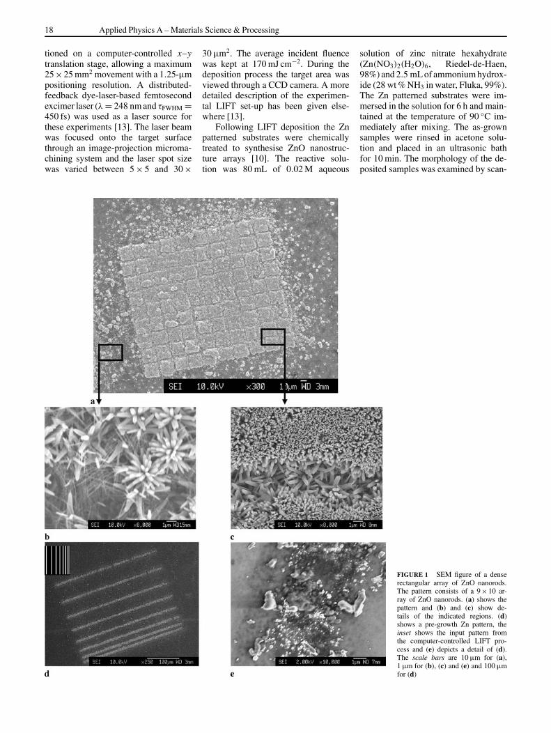
FIGURE 4 Plot of field-emission data: current density versus electric field. The inset shows the FNplot for the field-emission data
with the receiver–target either in con-tact with each other or at a distance of25 µm [16].
The overall quality of the patterns ofaligned ZnO nanorods can be estimatedvia XRD. Figure 2 shows the XRD spec-trum obtained for the 20-µm pixel sizepattern; this spectrum is typical for anypattern with pixel size > 10 µm. Allthe arrays grown exhibit the θ/2θ XRDlines that can be indexed to the hex-agonal würtzite structure of ZnO. Nocharacteristic peaks of Zn or other im-purities were observed. The strongestfeature within the spectrum (by a fac-tor of 10) attributed to ZnO is the (002)diffraction, indicating that most of theZnO nanorods exhibit [0001] alignedgrowth.
An additional measure of quality isthe room-temperature PL of the nanorodarrays. PL spectra were recorded atdifferent locations on the surfaces ofthe samples. Figure 3 shows a typi-cal PL spectrum taken from the ZnOnanorod array. The characteristic near-band-edge transition of ZnO is observedas a narrow UV band emission centredat 386 nm in all the recorded spectra.Significant visible green (∼ 570 nm) ororange (∼ 680 nm) emission has alsobeen reported for ZnO nanorods andthe emission wavelength is an indicatorfor the growth conditions and tempera-tures. The broad green–yellow emis-sion, centred at ∼ 570 nm, observed inthe PL spectra (as shown in Fig. 3) hasbeen reported previously in hydrother-mal growth [17] and has been associatedwith both zinc interstitials and oxygenvacancies [18].
Figure 4 shows a plot of the cur-rent density versus field emission char-acteristic curves of the samples. Sev-eral emission cycles were recorded inorder for the J–E curves to becomerelatively stable and reproducible. Thethreshold field is ∼ 5 V/µm, a value thatis in good agreement with the one re-ported in [19] for the emission of ZnOnanoneedle arrays fabricated throughvapour-phase growth. The increase ofbias voltage above the threshold dras-tically increases the field-emission cur-rent according to a Fowler–Nordheim(FN) tunnelling process until a satu-ration point is reached. In analysingthe field-emission data we adopted theFN analysis [20] of field-assisted tun-nelling, which is widely used to describethe relationship between the currentdensity J and the local field at the emit-ter Eloc, which is usually related to theaverage field E as follows:
Eloc = βE = βV
d. (1)
In (1), V is the applied voltage bias, dis the interelectrode spacing and β is thefield-enhancement factor. The FN law isexpressed as
J = A (βE)2 exp
(−bFN
βE
). (2)
In (2), A is a constant that dependson the surface structure [19], bFN= 0.94BΦ3/2 with B = 6.83 ×10⁷
V cm−1 eV−3/2, while Φ is the workfunction of the material in eV. The insetof Fig. 4 depicts the Fowler–Nordheimplot for the emission data. Assum-ing a work function of Φ = 5.3 eV for
ZnO [21], the corresponding enhance-ment factor β determined from the slopeof this line is 660.
For a single nanorod the field-en-hancement factor β is strongly depen-dent on the nanorod radius. Accordingto a simple model [22] the far-fieldvalue of the enhancement factor can befitted as βsingle
∼= 5.93 + 0.73(h/r) for100 < h/r < 500 and βsingle
∼= 2+ (h/r)for h/r < 40, where h and r are theheight and the radius of the rod, respec-tively. The corresponding theoreticalenhancement factor for 1-µm height and50-nm radius in our case is βsingle = 22,a value that is considerably lower thanthe experimental one. The differencecan be attributed to the influence of thefinite anode distance, as compared to therod height [23], or to the morphologicalcharacteristics of the rods that inhibit theaccurate estimation of the local field atone emitter [21].
4 Conclusions
In summary, [0001] orderedpixels of ZnO nanorod arrays have beenproduced successfully via combiningLIFT, a laser-based direct-write tech-nique to write the precursor Zn pixels,and chemical growth of ZnO nanorodsonto the Zn precursor pattern. Via thecombination of both techniques an over-all low-temperature (below 100 ◦C) pro-duction method for ZnO nanorods witha minimum of steps has been developed.The produced nanorod arrays showgood alignment along the [0001] crystaldirection and show a room-temperaturePL signature typical for rods grown byhydrothermal processes. The rod arraysshow excellent field-emission proper-ties with a threshold field for emissionof 5 V/µm. This study indicates a sim-ple and low-temperature synthesis routeto micropatterned ZnO nanorod sur-faces that can be used as field-emissiondevices.
ACKNOWLEDGEMENTS The workwas in part supported by the Ultraviolet Laser Fa-cility operating at IESL-FORTH under ContractNo. RIII3-CT-2003-506350. VD thanks the MarieCurie EST with Contract No. MEST- CT-2004-008048. FC thanks EPSRC for a post-doctoralfellowship grant at the Life Sciences Interface.The authors would like to acknowledge S. Chris-toulakis and G. Kiriakidis for the preparationof the sputtered Zn targets, E. Stratakis andE. Spanakis for their input in field-emission meas-urements and A. Egglezis for his assistance withfemtosecond laser experiments.
KLINI et al. ZnO nanorod micropatterning via laser-induced forward transfer 21
Appendix
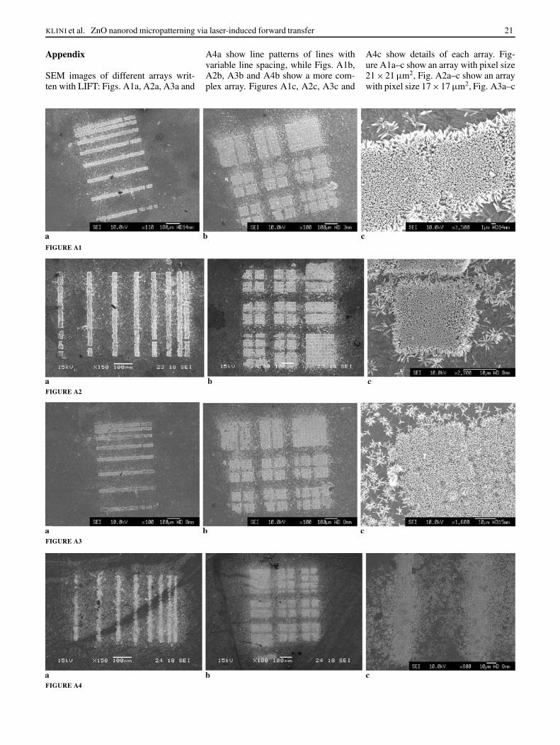
SEM images of different arrays writ-ten with LIFT: Figs. A1a, A2a, A3a and
FIGURE A1
FIGURE A2
FIGURE A3
FIGURE A4
A4a show line patterns of lines withvariable line spacing, while Figs. A1b,A2b, A3b and A4b show a more com-plex array. Figures A1c, A2c, A3c and
A4c show details of each array. Fig-ure A1a–c show an array with pixel size21 ×21 µm2, Fig. A2a–c show an arraywith pixel size 17×17 µm2, Fig. A3a–c

22 Applied Physics A – Materials Science & Processing
show an array with pixel size 8.5 ×8.5 µm2 and Fig. A4a–c show an ar-ray with pixel size 4.2 ×4.2 µm2. Fig-ure A4c indicates that the quality of thepatterns does deteriorate at pixel sizeslower than 5 µm; although the line pat-tern is still observable in the picture, theinterline spacing is filled with flower-like ZnO deposits.
REFERENCES
1 M.H. Huang, S. Mao, H. Feick, H. Yan,Y. Wu, H. Kind, E. Weber, R. Russo, P. Yang,Science 292, 1897 (2001)
2 M. Hiramatsu, K. Imaeda, N. Horio,M. Nawata, J. Vac. Sci. Technol. A 16, 669(1998)
3 H. Ohno, Science 281, 951 (1998)4 T.Y. Liu, H.C. Liao, C.C. Lin, S.H. Hu,
S.Y. Chen, Langmuir 22, 5804 (2006)
5 J.H. He, J.H. Hsu, C.W. Wang, H.N. Lin,L.J. Chen, Z.L. Wang, J. Phys. Chem. B 110,50 (2006)
6 Y. Sun, G.M. Fuge, M.N.R. Ashfold, Chem.Phys. Lett. 396, 21 (2004)
7 R. Liu, A.A. Vertegel, E.W. Bohannan,T.A. Sorenson, J.A. Switzer, Chem. Mater.13, 508 (2001)
8 L. Vayssieres, Adv. Mater. 15, 464 (2003)9 Y. Huang, X. Duan, Q. Wei, C.M. Lieber,
Science 291, 630 (2001)10 Y. Tak, K. Yong, J. Phys. Chem. B 109,
19 263 (2005)11 L.E. Greene, M. Law, D.H. Tan, M. Montano,
J. Goldberger, G. Somorjai, P. Yang, NanoLett. 5, 1231 (2005)
12 S.H. Lee, H.J. Lee, D. Oh, S.W. Lee, H. Goto,R. Buckmaster, T. Yasukawa, T. Matsue,S.K. Hong, H.C. Ko, M.W. Cho, T. Yao,J. Phys. Chem. B 110, 3856 (2006)
13 I. Zergioti, S. Mailis, N.A. Vainos, P. Papa-konstantinou, C. Kalpouzos, C.P. Grigoro-poulos, C. Fotakis, Appl. Phys. A 66, 579(1998)
14 V. Zorba, P. Tzanetakis, C. Fotakis, E. Spa-nakis, D.G. Papazoglou, I. Zergioti, Appl.Phys. Lett. 88, 081 103 (2006)
15 D.G. Papazoglou, A. Karaiskou, I. Zergioti,C. Fotakis, Appl. Phys. Lett. 81, 1594 (2002)
16 D.A. Willis, V. Grosu, Appl. Phys. Lett. 86,244 103 (2005)
17 Y. Sun, G.M. Fuge, N.A. Fox, D.J. Riley,M.N.R. Ashfold, Adv. Mater. 17, 2477 (2005)
18 X. Liu, X. Wu, H. Cao, R.P.H. Chang,J. Appl. Phys. 95, 3141 (2004)
19 Y.W. Zhu, H.Z. Zhang, X.C. Sun, S.Q. Feng,J. Xu, Q. Zhao, B. Xiang, R.M. Wang,D.P. Yu, Appl. Phys. Lett. 83, 144 (2003)
20 A. Modinos, Field, Thermionic and Sec-ondary Electron Emission Spectroscopy(Plenum, New York, 1984)
21 Q. Zhao, H.Z. Zhang, Y.W. Zhu, S.Q. Feng,X.C. Sun, J. Xu, D.P. Yu, Appl. Phys. Lett.86, 203 115 (2005)
22 G.C. Kokkorakis, A. Modinos, J.P. Xan-thakis, J. Appl. Phys. 91, 4580 (2002)
23 A. Lewis, B.W. Alphenaar, H. Ahmed, Appl.Phys. Lett. 79, 1348 (2001)
Related Documents