Activating ZnO nanorod photoanodes in visible light by Cu ion implantation Meng Wang, Feng Ren, Guangxu Cai, Yichao Liu, Shaohua Shen ( ), Liejin Guo Nano Res., Just Accepted Manuscript • DOI: 10.1007/s12274-014-0401-7 http://www.thenanoresearch.com on December 16, 2013 © Tsinghua University Press 2014 Just Accepted This is a “Just Accepted” manuscript, which has been examined by the peer‐review process and has been accepted for publication. A “Just Accepted” manuscript is published online shortly after its acceptance, which is prior to technical editing and formatting and author proofing. Tsinghua University Press (TUP) provides “Just Accepted” as an optional and free service which allows authors to make their results available to the research community as soon as possible after acceptance. After a manuscript has been technically edited and formatted, it will be removed from the “Just Accepted” Web site and published as an ASAP article. Please note that technical editing may introduce minor changes to the manuscript text and/or graphics which may affect the content, and all legal disclaimers that apply to the journal pertain. In no event shall TUP be held responsible for errors or consequences arising from the use of any information contained in these “Just Accepted” manuscripts. To cite this manuscript please use its Digital Object Identifier (DOI®), which is identical for all formats of publication. Nano Research DOI 10.1007/s12274‐014‐0401‐7

Welcome message from author
This document is posted to help you gain knowledge. Please leave a comment to let me know what you think about it! Share it to your friends and learn new things together.
Transcript

Nano Res
1
Activating ZnO nanorod photoanodes in visible light by
Cu ion implantation
Meng Wang, Feng Ren, Guangxu Cai, Yichao Liu, Shaohua Shen (), Liejin Guo Nano Res., Just Accepted Manuscript • DOI: 10.1007/s12274-014-0401-7 http://www.thenanoresearch.com on December 16, 2013 © Tsinghua University Press 2014
Just Accepted
This is a “Just Accepted” manuscript, which has been examined by the peer‐review process and has been
accepted for publication. A “Just Accepted” manuscript is published online shortly after its acceptance,
which is prior to technical editing and formatting and author proofing. Tsinghua University Press (TUP)
provides “Just Accepted” as an optional and free service which allows authors to make their results available
to the research community as soon as possible after acceptance. After a manuscript has been technically
edited and formatted, it will be removed from the “Just Accepted” Web site and published as an ASAP
article. Please note that technical editing may introduce minor changes to the manuscript text and/or
graphics which may affect the content, and all legal disclaimers that apply to the journal pertain. In no event
shall TUP be held responsible for errors or consequences arising from the use of any information contained
in these “Just Accepted” manuscripts. To cite this manuscript please use its Digital Object Identifier (DOI®),
which is identical for all formats of publication.
Nano Research DOI 10.1007/s12274‐014‐0401‐7
1
TABLE OF CONTENTS (TOC)
Activating ZnO Nanorod Photoanodes in Visible Light
by Cu Ion Implantation
Meng Wang1, Feng Ren2, Guangxu Cai2, Yichao Liu2,
Shaohua Shen1*, Liejin Guo1
Xi’an Jiaotong University, China
Wuhan University, China
Page Numbers.
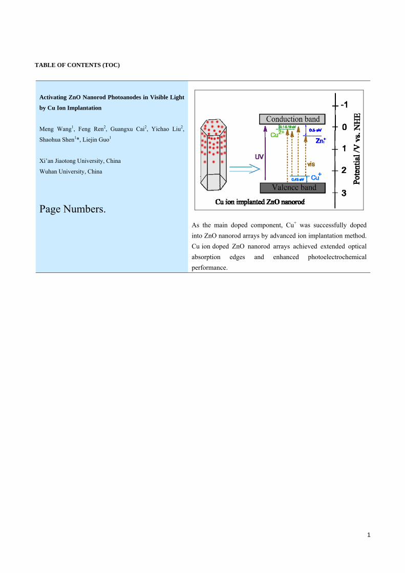
As the main doped component, Cu+ was successfully doped
into ZnO nanorod arrays by advanced ion implantation method.
Cu ion doped ZnO nanorod arrays achieved extended optical
absorption edges and enhanced photoelectrochemical
performance.
2
Activating ZnO Nanorod Photoanodes in Visible Light by Cu Ion Implantation
Meng Wang1, Feng Ren2, Guangxu Cai2, Yichao Liu2, Shaohua Shen1 (), Liejin Guo1
1 International Research Centre for Renewable Energy, State Key Laboratory of Multiphase Flow in Power Engineering, Xi’an
Jiaotong University, Shaanxi 710049, China. Email: [email protected] 2 School of Physics and Technology, Center for Ion Beam Application, Wuhan University, Wuhan 430072, P. R. China
Received: day month year / Revised: day month year / Accepted: day month year (automatically inserted by the publisher) © Tsinghua University Press and Springer-Verlag Berlin Heidelberg 2011
ABSTRACT Utilization of visible light is of crucial importance for exploiting efficient semiconductor catalysts for solar
water splitting. In this study, an advanced ion implantation method was utilized to dope Cu ions into ZnO
nanorod arrays for photoelectrochemical water splitting in visible light. XRD and XPS results revealed that
Cu+ together with a small amount of Cu2+ were highly dispersed within the ZnO nanorod arrays. Cu ion
doped ZnO nanorod arrays displayed extended optical absorption and enhanced photoelectrochemical
performance under visible light illumination (λ > 420 nm). A considerable photocurrent density of 18 μA/cm2
at 0.8 V (vs. SCE) was achieved, which was about 11 times higher than that of bare ZnO nanorod arrays. This
study proposes that ion implantation could be an effective approach for developing novel
visible‐light‐driven photocatalytic materials for water splitting.
KEYWORDS Ion implantation; Cu ion doping; ZnO nanorods; photoanode; water splitting
1 Introduction
ZnO has been one of the most widely investigated
materials for solar water splitting, due to its
excellent properties such as thermal stability, low
cost, non‐toxic and appropriate conduction/valence
band edges [1‐7]. However, because of the wide
band gap, ZnO can only respond to ultraviolet (UV)
light, which accounts for only 4% in the solar
spectrum. To extend its optical absorbance band
edge to visible light range, in the past decades,
many attempts, for example, doping with metal or
non metal ions [8‐10], sensitizing with organic dyes
[11‐13], narrow band gap semiconductor quantum
Nano Res DOI (automatically inserted by the publisher) Research Article
————————————
Address correspondence to Shaohua Shen, [email protected]
3
dots like CdS, CdSe and CdTe [14‐18] and
nano‐sized plasmonic nanoparticles [19‐21] have
been carried out to make ZnO photoactive under
visible light irradiation.
Doping with metal ions is a very common method
to create impurity levels in the forbidden gap and to
narrow the band gap for utilizing visible light. The
impurity levels which locate above the valence band
or below the conduction band act as acceptor levels
or donor levels, respectively. Both acceptor levels
and donor levels make the semiconductors
responsive to visible light. Many approaches such
as co‐precipitation [22, 23], sol‐gel [2, 24], chemical
vapor deposition [25, 26], hydrothermal [27], and
advanced ion implantation, etc. [28‐33], were
implemented to dope metal ions into wide band
gap materials. Comparing these different
approaches, metal ions introduced by traditional
chemical doping methods are always unstable.
After post annealing treatment, they aggregate on
the surface of substrate materials, which can act as
recombination centres for photo‐induced electrons
and holes [28]. On the contrary, the physical doping
method such as advanced ion implantation method
can make the doped metal ions inject into the bulk
of substrate materials and exist in a highly
dispersed state. Therefore, ion implantation can
modify the bulk electronic properties of substrate
materials, and has been considered as an effective
approach to incorporate metal ions into TiO2 crystal
to improve its optical absorption properties. Several
far‐reaching reviews have been published [28, 32,
33], in which the effects of metal ion implantation
for extending the optical absorption edges and
improving the photocatalytic activity of TiO2 were
discussed. It was indicated that metal ion
implantation with Fe, Ni, Mn, V, and Cr caused
obvious red shift in the optical absorption spectra of
TiO2 photocatalysts, whereas Ti, Mg, or Ar ion
implanted TiO2 exhibited no obvious red shift in the
optical absorption spectra, showing that the red
shift was not resulted from the implantation
approach itself, but induced by the interaction of
dopants and TiO2 catalyst. However, most of the
metal ion implanted TiO2 photocatalysts were
utilized for decomposing organic pollutes. Metal
ion implanted TiO2 or ZnO films utilized as
effective phtoanodes for efficient water splitting
were rarely reported. In our serials of experiments,
various elements such as Cu, N, V, etc. have been
doped to different substrates such as ZnO and TiO2
photoanodes by ion implantation method. Both
doped ZnO and TiO2 photoanodes exhibited
extended optical absorption edges and enhanced
photoelectrochemical (PEC) performance under
visible light (λ > 420 nm). Detailed investigations
about these results are in progress.
In the present study, ZnO nanorod arrays were
hydrothermally grown on the fluorine‐doped tin
oxide (FTO) substrate, and further doped with
different fluences of Cu ions by the ion implantation
technique. A systematic investigation was conducted
to reveal the influence of Cu dopants on the
physicochemical properties and PEC performance of
Cu ion doped ZnO nanorod photoanodes.
2 Experimental
2.1 Synthesis procedure
(1) ZnO nanorod arrays were prepared via a
hydrothermal method as described in previous
reports [34, 35], with minor modification. ZnO
nanorod arrays were grown on the fluorine‐doped
tin oxide (FTO) substrate. FTO substrate (TEC‐15,
15 Ω/sp) were cleaned by ultrasonic cleaning in
acetone, de‐ionized water and ethanol, for 30 min
respectively, and then dried in nitrogen flow. 0.1 M
zinc acetate (Zn(CH3COO)2∙2H2O) in methanol was
spin‐coated on FTO glasses at 2000 rpm for 25 s,
which was repeated for 8 times. Then the substrate
was annealed in air at 350 °C for 30 min with a
ramping rate of 5 °C /min. The obtained ZnO
seeded FTO glass was put into a mixed aqueous
4
solution of zinc nitrate (Zn(NO3)2∙6H2O) and
hexamethylenetetramine (C6H12N4) (0.05 mol/L),
and maintained at 90 °C for 24 h. Finally, ZnO
nanorod arrays were obtained by post annealing
treatment at 450 °C for 30 min with a ramping rate
of 5 °C/min.
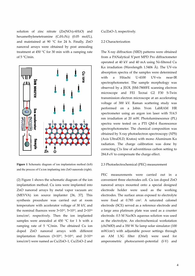
Figure 1 Schematic diagram of ion implantation method (left)
and the process of Cu ion implanting into ZnO nanorods (right).
(2) Figure 1 shows the schematic diagram of the ion
implantation method. Cu ions were implanted into
ZnO nanorod arrays by metal vapor vacuum arc
(MEVVA) ion source implanter [36, 37]. This
synthesis procedure was carried out at room
temperature with accelerator voltage of 30 kV, and
the nominal fluences were 3×10¹⁵, 5×10¹⁵, and 2×10¹⁶
ions/cm2, respectively. Then the ion implanted
samples were annealed at 450 °C for 1 h with a
ramping rate of 5 °C/min. The obtained Cu ion
doped ZnO nanorod arrays with different
implantation fluences (3×10¹⁵, 5×10¹⁵, and 2×10¹⁶
ions/cm2) were named as Cu/ZnO–1, Cu/ZnO–2 and
Cu/ZnO–3, respectively.
2.2 Characterization
The X‐ray diffraction (XRD) patterns were obtained
from a PANalytical X’pert MPD Pro diffractometer
operated at 40 kV and 40 mA using Ni‐filtered Cu
Kα irradiation (Wavelength 1.5406 Å). The UV‐vis
absorption spectra of the samples were determined
with a Hitachi U‐4100 UV‐vis near‐IR
spectrophotometer. The sample morphology was
observed by a JEOL JSM‐7800FE scanning electron
microscope and FEI Tecnai G2 F30 S‐Twin
transmission electron microscope at an accelerating
voltage of 300 kV. Raman scattering study was
performed on a Jobin Yvon LabRAM HR
spectrometer using an argon ion laser with 514.5
nm irradiation at 20 mW. Photoluminescence (PL)
spectra were tested on a PTI QM‐4 fluorescence
spectrophotometer. The chemical composition was
obtained by X‐ray photoelectron spectroscopy (XPS)
(Axis UltraDLD, Kratos) with mono Aluminum Kα
radiation. The charge calibration was done by
correcting C1s line of adventitious carbon setting to
284.8 eV to compensate the charge effect.
2.3 Photoelectrochemical (PEC) measurement
PEC measurements were carried out in a
convenient three electrodes cell. Cu ion doped ZnO
nanorod arrays mounted onto a special designed
electrode holder were used as the working
electrodes. The surface areas exposed to electrolyte
were fixed at 0.785 cm2. A saturated calomel
electrode (SCE) served as a reference electrode and
a large area platinum plate was used as a counter
electrode. 0.5 M Na2SO4 aqueous solution was used
as the electrolyte. An electrochemical workstation
(chi760D) and a 350 W Xe lamp solar simulator (100
mW/cm2) with adjustable power settings through
an AM 1.5G filter (Oriel) were used for
amperometric photocurrent–potential (I‐V) and
5
photocurrent–time (I‐t) measurements, with a 420
nm cut‐off filter used to prevent UV light.
Mott‐Schottky measurement in dark was performed
in a 0.5 M Na2SO4 electrolyte at the frequency of 1
kHz, with Ag/AgCl as the reference electrode.
3 Results and Discussion
3.1 Morphology analysis
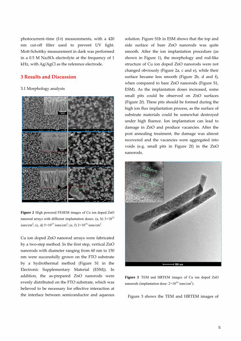
Figure 2 High powered FESEM images of Cu ion doped ZnO
nanorod arrays with different implantation doses: (a, b) 3×10¹⁵
ions/cm2; (c, d) 5×10¹⁵ ions/cm2; (e, f) 2×10¹⁶ ions/cm2.
Cu ion doped ZnO nanorod arrays were fabricated
by a two‐step method. In the first step, vertical ZnO
nanorods with diameter ranging from 60 nm to 150
nm were successfully grown on the FTO substrate
by a hydrothermal method (Figure S1 in the
Electronic Supplementary Material (ESM)). In
addition, the as‐prepared ZnO nanorods were
evenly distributed on the FTO substrate, which was
believed to be necessary for effective interaction at
the interface between semiconductor and aqueous
solution. Figure S1b in ESM shows that the top and
side surface of bare ZnO nanorods was quite
smooth. After the ion implantation procedure (as
shown in Figure 1), the morphology and rod‐like
structure of Cu ion doped ZnO nanorods were not
changed obviously (Figure 2a, c and e), while their
surface became less smooth (Figure 2b, d and f),
when compared to bare ZnO nanorods (Figure S1,
ESM). As the implantation doses increased, some
small pits could be observed on ZnO surfaces
(Figure 2f). These pits should be formed during the
high ion flux implantation process, as the surface of
substrate materials could be somewhat destroyed
under high fluence. Ion implantation can lead to
damage in ZnO and produce vacancies. After the
post annealing treatment, the damage was almost
recovered and the vacancies were aggregated into
voids (e.g. small pits in Figure 2f) in the ZnO
nanorods.
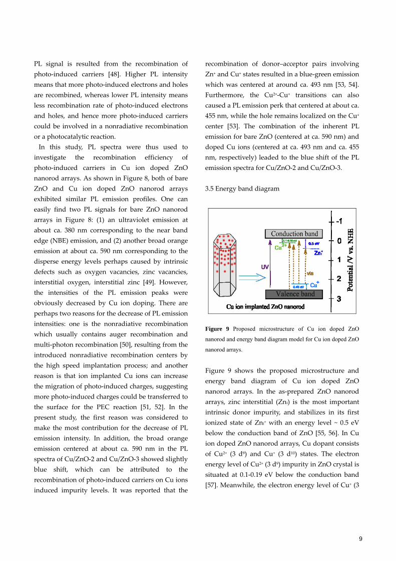
Figure 3 TEM and HRTEM images of Cu ion doped ZnO
nanorods (implantation dose: 2×10¹⁶ ions/cm2).
Figure 3 shows the TEM and HRTEM images of

6
Cu ion doped ZnO nanorods. The d‐spacing of
lattice fringes of ZnO nanorod was ca. 0.26 nm,
corresponding to the (002) planes of hexagonal
ZnO(reference code: 01‐089‐0510) [35]. Nevertheless,
aggregated Cu2O or CuO particles and lattice
fringes belong to copper oxides were not found in
SEM and TEM images, which revealed that the
implanted Cu ions were highly dispersed in ZnO
crystal.
3.2 Optical and structural properties
Figure 4 displays the UV‐vis absorption spectra of
bare ZnO and Cu ion doped ZnO nanorod arrays.
The bare ZnO nanorod arrays showed only optical
absorption ability in ultraviolet region, solar light
with wavelength longer than ca. 390 nm could not
be utilized. After Cu ion implantation, all the
samples displayed obvious optical absorption
ability in visible region. The absorption edges
showed a gradual red shift as the implantation
doses increased. This should be related to the
impurity levels in the forbidden gap of ZnO created
by Cu dopant.
Figure 4 UV-vis absorption spectra of Cu ion doped ZnO
nanorod arrays with the spectrum of bare ZnO nanorod arrays
as a reference.
Figure 5 (a) XRD patterns of various Cu ion doped ZnO
nanorod arrays at different implantation doses with the data of
ZnO nanorod arrays as a reference, and (b) XRD patterns of the
same samples with the diffraction angle (2θ) in the range of 33°
to 37°.
Crystal structures of ZnO and Cu ion doped ZnO
nanorod arrays were characterized by X‐ray
diffraction (XRD) patterns. As shown in Figure 5, all
the samples present sharp, narrow and well distinct
peaks, which is an indication of crystalline nature.
For either bare ZnO or Cu ion doped ZnO nanorod
arrays, six peaks arise at 2θ = 31.8°, 34.4°, 36.3°,
47.6°, 62.9° and 68.0° which could be assigned to
(100), (002), (101), (102), (103) and (112) planes of
wurtzite ZnO (reference code: 01‐089‐0510),

7
respectively [38]. No other peaks related to
impurities were detected in XRD patterns,
indicating that the films were only consisted of bare
ZnO nanorods or Cu ion doped ZnO nanorods. The
most intensive peak was observed at 2θ = 34.43°,
corresponding to the (002) plane, suggesting that
ZnO nanorods grow along (001) direction which
has already been proved by SEM (Figure 2) and
TEM images (Figure 3). After Cu ion implantation,
the XRD diffraction intensity of (002) peak
decreased obviously. From the detailed view of (002)
diffraction patterns shown in Figure 5b, the peak
position was found to shift to lower angle, which
indicated that Cu+ was the main dopant in doped
ZnO nanorod arrays. Cu ions could exist at
different valence states of +1 and +2 for Cu ion
doped ZnO nanorod arrays. The radius of Cu+, Cu2+
and Zn2+ ions were 0.096, 0.072 and 0.074 nm,
respectively. Because the diameter of Cu+ is larger
than that of Zn2+ [39], the doping of Cu+ in ZnO
crystal made the XRD peaks shift to lower angle.
Furthermore, for bare ZnO, Cu/ZnO‐1, Cu/ZnO‐2
and Cu/ZnO‐3, the (002) diffraction peak displayed
a gradual shift to lower angle, revealing that the
amount of Cu+ doped in ZnO increased gradually
as the implantation doses increased.
As illustrated in Figure 6, Raman modes observed
at 436 cm‐1 and 980 cm‐1 are assigned to the E2 (high)
and 2TO modes, respectively. The broad bands
around 1100 cm−1 should correspond to 2LO
(longitudinal‐optical) features. However, the
description is somewhat doubtful, because this
mode at 1100 cm−1 can be also observed at relative
region for the FTO substrate [38]. For Cu ion doped
ZnO nanorod arrays, Raman modes at 436 cm‐1 and
980 cm‐1 were also observed, indicating wurtzite
ZnO crystal structure was not destroyed by ion
implantation approach, which matched well with
the XRD patterns (Figure 5). Except for the
characteristic Raman peaks (436 cm‐1 and 980 cm‐1)
for ZnO, another intensive peak around 580 cm‐1
was also obtained for Cu ion doped ZnO nanorod
arrays. This Raman band was assigned to the silent
B1 (high) mode [41], which could be resulted from
disorder‐activated Raman scattering (DARS) [42]. A
possible explanation for this scattering is the
breakdown of the translational symmetry of the
crystal structure caused by defects or impurities
formed during ion implantation. The change of the
translational symmetry relaxed the conservation of
wave vector, and then led to scattering by phonons
in the host materials that have wave vectors far
from the zone center [41]. Similar phenomenon was
also reported by Pan et al. [40], that additional
vibration mode at around 580 cm‐1 was observed for
N ion doped ZnO nanorod arrays. Furthermore,
many other wurtzite materials such as InN, GaN,
AlN, and Al1−xGaxN showed disorder‐activated
Raman scattering as well [43‐45]. Together with
XRD patterns, and UV‐vis absorption spectra, the
Raman results indicated that Cu ions could be
doped into ZnO successfully through the advanced
ion implantation approach.
Figure 6 Raman spectra of bare ZnO and Cu ion doped ZnO
nanorod arrays with different Cu ion implantation doses.
3.3 Chemical states analysis
X‐ray photoelectron spectroscopy (XPS) analysis
was used to study the chemical compositions of Cu

8
ion doped ZnO nanorod arrays. From the survey
scan XPS spectra in Figure S2 (ESM), the peaks
corresponding to O, Zn, Cu and adventitious C
elements are observed. Figure S3 in ESM shows that
the binding energies of Zn 2p3/2 and 2p1/2 levels
located at 1021.3 eV and 1044.6 eV, respectively,
which confirms the formation of ZnO crystal phase.
Figure 7 (a) XPS Cu 2p spectra for Cu ion doped ZnO nanorod
arrays with implantation dose at 2×10¹⁶ ions/cm2. (b) XPS
etching profile of Cu/ZnO-3.
To confirm the valence states of doped Cu ions,
XPS Cu 2p spectra were also investigated (Figure 7).
Cu 2p1/2 and Cu 2p3/2 peaks can be coherently fitted
by two components [46, 47]. The binding energy
located at 932.2 eV and 951.8 eV were contributed
from Cu+, while those located at 934.3 eV and 953.6
eV were attributed to Cu2+. Additionally, peak area
for Cu+ was much larger than that of Cu2+,
suggesting Cu+ is the main doped component which
matched well with the XRD results (Figure 5).
Figure S4 and 7b illustrate the distribution of Cu
dopant as a function of etching time and etching
depth for Cu ion doped ZnO nanorod arrays
(taking Cu/ZnO‐3 as the representative sample).
This measurement was operated by serial XPS
measurements during controlled Ar+ etching, and
the transition method from etching time to etching
rate was discussed in detail in the ESM. According
to the nature of ion implantation technique (Figure
1), it is reasonable that the concentration of Cu
dopant decreased gradually with the elongated
etching time (i.e., the increasing etching depth).
Thus, as shown in the inset of Figure 7b, gradient
Cu ion doped ZnO nanorod arrays were acquired
by ion implantation method.
3.4 Photoluminescence properties
Figure 8 PL spectra of bare ZnO and various Cu ion doped
ZnO nanorod arrays. Excitation: 337 nm from a 75 W Xe lamp.
To study how Cu dopant influences the
luminescence of ZnO nanorod arrays,
photoluminescence (PL) spectra were measured for
Cu ion doped ZnO nanorod arrays. Generally, the
9
PL signal is resulted from the recombination of
photo‐induced carriers [48]. Higher PL intensity
means that more photo‐induced electrons and holes
are recombined, whereas lower PL intensity means
less recombination rate of photo‐induced electrons
and holes, and hence more photo‐induced carriers
could be involved in a nonradiative recombination
or a photocatalytic reaction.
In this study, PL spectra were thus used to
investigate the recombination efficiency of
photo‐induced carriers in Cu ion doped ZnO
nanorod arrays. As shown in Figure 8, both of bare
ZnO and Cu ion doped ZnO nanorod arrays
exhibited similar PL emission profiles. One can
easily find two PL signals for bare ZnO nanorod
arrays in Figure 8: (1) an ultraviolet emission at
about ca. 380 nm corresponding to the near band
edge (NBE) emission, and (2) another broad orange
emission at about ca. 590 nm corresponding to the
disperse energy levels perhaps caused by intrinsic
defects such as oxygen vacancies, zinc vacancies,
interstitial oxygen, interstitial zinc [49]. However,
the intensities of the PL emission peaks were
obviously decreased by Cu ion doping. There are
perhaps two reasons for the decrease of PL emission
intensities: one is the nonradiative recombination
which usually contains auger recombination and
multi‐photon recombination [50], resulting from the
introduced nonradiative recombination centers by
the high speed implantation process; and another
reason is that ion implanted Cu ions can increase
the migration of photo‐induced charges, suggesting
more photo‐induced charges could be transferred to
the surface for the PEC reaction [51, 52]. In the
present study, the first reason was considered to
make the most contribution for the decrease of PL
emission intensity. In addition, the broad orange
emission centered at about ca. 590 nm in the PL
spectra of Cu/ZnO‐2 and Cu/ZnO‐3 showed slightly
blue shift, which can be attributed to the
recombination of photo‐induced carriers on Cu ions
induced impurity levels. It was reported that the
recombination of donor–acceptor pairs involving
Zn+ and Cu+ states resulted in a blue‐green emission
which was centered at around ca. 493 nm [53, 54].
Furthermore, the Cu2+‐Cu+ transitions can also
caused a PL emission perk that centered at about ca.
455 nm, while the hole remains localized on the Cu+
center [53]. The combination of the inherent PL
emission for bare ZnO (centered at ca. 590 nm) and
doped Cu ions (centered at ca. 493 nm and ca. 455
nm, respectively) leaded to the blue shift of the PL
emission spectra for Cu/ZnO‐2 and Cu/ZnO‐3.
3.5 Energy band diagram
Figure 9 Proposed microstructure of Cu ion doped ZnO
nanorod and energy band diagram model for Cu ion doped ZnO
nanorod arrays.
Figure 9 shows the proposed microstructure and
energy band diagram of Cu ion doped ZnO
nanorod arrays. In the as‐prepared ZnO nanorod
arrays, zinc interstitial (Zni) is the most important
intrinsic donor impurity, and stabilizes in its first
ionized state of Zni+ with an energy level ~ 0.5 eV
below the conduction band of ZnO [55, 56]. In Cu
ion doped ZnO nanorod arrays, Cu dopant consists
of Cu2+ (3 d9) and Cu+ (3 d10) states. The electron
energy level of Cu2+ (3 d9) impurity in ZnO crystal is
situated at 0.1‐0.19 eV below the conduction band
[57]. Meanwhile, the electron energy level of Cu+ (3
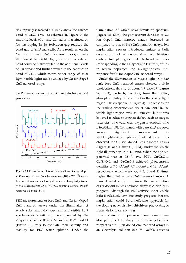
10
d10) impurity is located at 0.45 eV above the valence
band of ZnO. Thus, as schemed in Figure 9, the
impurity levels (Cu2+ and Cu+ states) introduced by
Cu ion doping in the forbidden gap reduced the
band gap of ZnO markedly. As a result, when the
Cu ion doped ZnO nanorod arrays were
illuminated by visible light, electrons in valence
band could be firstly excited to the additional levels
of Cu dopant and further excited to the conduction
band of ZnO, which means wider range of solar
light (visible light) can be utilized by Cu ion doped
ZnO nanorod arrays.
3.6 Photoelectrochemical (PEC) and electrochemical
properties
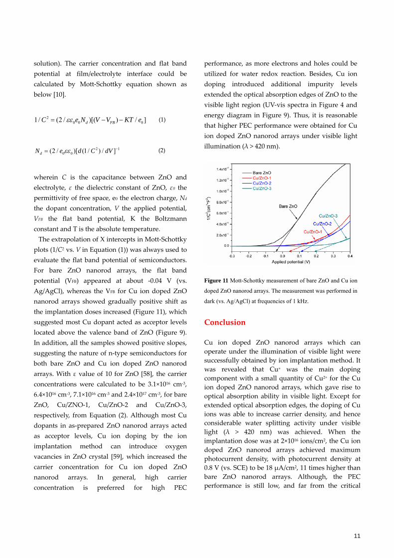
Figure 10 Photocurrent plots of bare ZnO and Cu ion doped
ZnO nanorod arrays. (A solar simulator (100 mW/cm2) with a
filter of 420 nm was used as light sources with applied potential
of 0.8 V, electrolyte: 0.5 M Na2SO4, counter electrode: Pt, and
reference electrode: SCE)
PEC measurements of bare ZnO and Cu ion doped
ZnO nanorod arrays under the illumination of
whole solar simulator spectrum and visible light
spectrum (λ > 420 nm) were operated by the
Amperometric I‐V (Figure S5 and S6, ESM) and I‐t
(Figure 10) tests to evaluate their activity and
stability for PEC water splitting. Under the
illumination of whole solar simulator spectrum
(Figure S5, ESM), the photocurrent densities of Cu
ion doped ZnO nanorod arrays decreased as
compared to that of bare ZnO nanorod arrays. Ion
implantation process introduced surface or bulk
defects can act as nonradiative recombination
centers for photogenerated electron‐hole pairs
(corresponding to the PL spectra in Figure 8), which
in return depressed the UV‐light‐driven PEC
response for Cu ion doped ZnO nanorod arrays.
Under the illumination of visible light (λ > 420
nm), bare ZnO nanorod arrays showed a little
photocurrent density of about 1.7 μA/cm2 (Figure
S6, ESM), probably, resulting from the trailing
absorption ability of bare ZnO in the visible light
region (Uv‐vis spectra in Figure 4). The reasons for
the trailing absorption ability of bare ZnO in the
visible light region was still unclear, but it was
believed to relate to intrinsic defects such as oxygen
vacancies, zinc vacancies, oxygen interstitial, zinc
interstitials [49]. Compared with bare ZnO nanorod
arrays, significant improvement in
visible‐light‐driven photocurrent density was
observed for Cu ion doped ZnO nanorod arrays
(Figure 10 and Figure S6, ESM), under the visible
light illumination (λ > 420 nm). When the applied
potential was at 0.8 V (vs. SCE), Cu/ZnO‐1,
Cu/ZnO‐2 and Cu/ZnO‐3 achieved photocurrent
densities of 7.5 μA/cm2, 9.7 μA/cm2 and 18 μA/cm2,
respectively, which were about 4, 6 and 11 times
higher than that of bare ZnO nanorod arrays. A
more detailed study to optimize the concentration
of Cu dopant in ZnO nanorod arrays is currently in
progress. Although the PEC activity under visible
light is relatively low, this study proposes that ion
implantation could be an effective approach for
developing novel visible‐light‐driven photocatalytic
materials for water splitting.
Electrochemical impedance measurement was
also performed to study the intrinsic electronic
properties of Cu ion doped ZnO nanorod arrays in
an electrolyte solution (0.5 M Na2SO4 aqueous
11
solution). The carrier concentration and flat band
potential at film/electrolyte interface could be
calculated by Mott‐Schottky equation shown as
below [10].
20 0 01/ (2 / )[( ) / ]d FBC e N V V KT e (1)
2 10 0(2 / )[ (1 / ) / ]dN e d C dV (2)
wherein C is the capacitance between ZnO and
electrolyte, ε the dielectric constant of ZnO, ε0 the
permittivity of free space, e0 the electron charge, Nd
the dopant concentration, V the applied potential,
VFB the flat band potential, K the Boltzmann
constant and T is the absolute temperature.
The extrapolation of X intercepts in Mott‐Schottky
plots (1/C2 vs. V in Equation (1)) was always used to
evaluate the flat band potential of semiconductors.
For bare ZnO nanorod arrays, the flat band
potential (VFB) appeared at about ‐0.04 V (vs.
Ag/AgCl), whereas the VFB for Cu ion doped ZnO
nanorod arrays showed gradually positive shift as
the implantation doses increased (Figure 11), which
suggested most Cu dopant acted as acceptor levels
located above the valence band of ZnO (Figure 9).
In addition, all the samples showed positive slopes,
suggesting the nature of n‐type semiconductors for
both bare ZnO and Cu ion doped ZnO nanorod
arrays. With ε value of 10 for ZnO [58], the carrier
concentrations were calculated to be 3.1×1016 cm‐3,
6.4×1016 cm‐3, 7.1×1016 cm‐3 and 2.4×1017 cm‐3, for bare
ZnO, Cu/ZNO‐1, Cu/ZnO‐2 and Cu/ZnO‐3,
respectively, from Equation (2). Although most Cu
dopants in as‐prepared ZnO nanorod arrays acted
as acceptor levels, Cu ion doping by the ion
implantation method can introduce oxygen
vacancies in ZnO crystal [59], which increased the
carrier concentration for Cu ion doped ZnO
nanorod arrays. In general, high carrier
concentration is preferred for high PEC
performance, as more electrons and holes could be
utilized for water redox reaction. Besides, Cu ion
doping introduced additional impurity levels
extended the optical absorption edges of ZnO to the
visible light region (UV‐vis spectra in Figure 4 and
energy diagram in Figure 9). Thus, it is reasonable
that higher PEC performance were obtained for Cu
ion doped ZnO nanorod arrays under visible light
illumination (λ > 420 nm).
Figure 11 Mott-Schottky measurement of bare ZnO and Cu ion
doped ZnO nanorod arrays. The measurement was performed in
dark (vs. Ag/AgCl) at frequencies of 1 kHz.
Conclusion
Cu ion doped ZnO nanorod arrays which can
operate under the illumination of visible light were
successfully obtained by ion implantation method. It
was revealed that Cu+ was the main doping
component with a small quantity of Cu2+ for the Cu
ion doped ZnO nanorod arrays, which gave rise to
optical absorption ability in visible light. Except for
extended optical absorption edges, the doping of Cu
ions was able to increase carrier density, and hence
considerable water splitting activity under visible
light (λ > 420 nm) was achieved. When the
implantation dose was at 2×10¹⁶ ions/cm2, the Cu ion
doped ZnO nanorod arrays achieved maximum
photocurrent density, with photocurrent density at
0.8 V (vs. SCE) to be 18 μA/cm2, 11 times higher than
bare ZnO nanorod arrays. Although, the PEC
performance is still low, and far from the critical

12
conversion efficiency for practical applications of
solar water splitting for hydrogen production, this
study presents a feasible approach for developing
novel visible‐light‐driven photocatalysts or
photoanodes.
Acknowledgements
The authors gratefully acknowledge the financial
support of the National Natural Science Foundation
of China (no. 51102194, no. 51121092), the Doctoral
Program of the Ministry of Education (no.
20110201120040) and the Nano Research Program of
Suzhou City (ZXG2013003). S. Shen is supported by
the Foundation for the Author of National Excellent
Doctoral Dissertation of P. R. China (No. 201335) and
the “Fundamental Research Funds for the Central
Universities”.
Electronic Supplementary Material: Supplementary
material (SEM images of bare ZnO nanorod arrays,
Survey‐scan XPS spectra of Cu/ZnO‐2, XPS Zn 2p
spectra of Cu/ZnO‐3 and I‐V plots of bare ZnO and
Cu/ZnO‐1) is available in the online version of this
article at http://dx.doi.org/10.1007/s12274‐***‐****‐*
References
[1] Tian, Z. R.; Voigt, J. A.; Liu, J.; McKenzie, B.; McDermott,
M. J.; Rodriguez, M. A.; Konishi, H.; Xu, H. Complex and
oriented ZnO nanostructures. Nat. Mater. 2003, 2, 821-826.
[2] Lakshmi, B. B.; Dorhout, P. K.; Martin, C. R. Sol−gel
template synthesis of semiconductor nanostructures. Chem.
Mater. 1997, 9, 857-862.
[3] Sakthivel, S.; Neppolian, B.; Shankar, M. V.; Arabindoo,
B.; Palanichamy, M.; Murugesan, V. Solar photocatalytic
degradation of Azo dye: Comparison of photocatalytic
efficiency of ZnO and TiO2. Sol. Energy Mater. Sol. Cells
2003, 77, 65-82.
[4] Yang, J. L.; An, S. J.; Park, W. I.; Yi, G. C.; Choi, W.
Photocatalysis using ZnO thin films and nanoneedles
grown by metal–organic chemical vapor deposition. Adv.
Mater. 2004, 16, 1661-1664.
[5] Wu, J.-J.; Tseng, C.-H. Photocatalytic properties of
nc-Au/ZnO nanorod composites. Appl. Catal. B 2006, 66,
51-57.
[6] Mansilla, H. D.; Villasenor, J.; Maturana, G.; Baeza, J.;
Freer, J.; Duran, N. ZnO-catalyzed photodegradation of
kraft black liquor. J. Photochem. Photobiol. A 1994, 78,
267-273.
[7] Gu, L.; Zheng, K.; Zhou, Y.; Li, J.; Mo, X.; Patzke, G. R.;
Chen, G. Humidity sensors based on ZnO/TiO2 core/shell
nanorod arrays with enhanced sensitivity. Sens. Actuat. B
2011, 159, 1-7.
[8] Akpan, U. G.; Hameed, B. H. The advancements in sol–gel
method of doped-TiO2 photocatalysts. Appl. Catal. A 2010,
375, 1-11.
[9] Das, S. C.; Green, R. J.; Podder, J.; Regier, T. Z.; Chang, G.
S.; Moewes, A. Band gap tuning in ZnO through Ni doping
via spray pyrolysis. J. Phys. Chem. C 2013, 117,
12745-12753.
[10] Yang, X.; Wolcott, A.; Wang, G.; Sobo, A.; Fitzmorris, R.
C.; Qian, F.; Zhang, J. Z.; Li, Y. Nitrogen-doped ZnO
nanowire arrays for photoelectrochemical water splitting.
Nano. Lett. 2009, 9, 2331-2336.
[11] Law, M.; Greene, L. E.; Johnson, J. C.; Saykally, R.; Yang,
P. Nanowire dye-sensitized solar cells. Nat. Mater. 2005, 4,
455-459.
[12] Huang, K.-C.; Chang, Y.-H.; Chen, C.-Y.; Liu, C.-Y.; Lin,
L.-Y.; Vittal, R.; Wu, C.-G.; Lin, K.-F.; Ho, K.-C.
Improved exchange reaction in an ionic liquid electrolyte
of a quasi-solid-state dye-sensitized solar cell by using
15-crown-5-functionalized MWCNT. J. Mater. Chem.
2011, 21, 18467-18474.
[13] Scho ̈lin, R.; Quintana, M. a.; Johansson, E. M. J.; Hahlin,
M.; Marinado, T.; Hagfeldt, A.; Rensmo, H. K. Preventing
dye aggregation on ZnO by adding water in the
dye-sensitization process. J. Phys. Chem. C 2011, 115,
19274-19279.
[14] Leschkies, K. S.; Divakar, R.; Basu, J.; Enache-Pommer,
E.; Boercker, J. E.; Carter, C. B.; Kortshagen, U. R.; Norris,
D. J.; Aydil, E. S. Photosensitization of ZnO nanowires
with CdSe quantum dots for photovoltaic devices. Nano.
Lett. 2007, 7, 1793-1798.
[15] Tang, Y.; Hu, X.; Chen, M.; Luo, L.; Li, B.; Zhang, L.
CdSe nanocrystal sensitized ZnO core-shell nanorod array
films: Preparation and photovoltaic properties. Electrochim.
13
Acta 2009, 54, 2742-2747.
[16] Bang, J. H.; Kamat, P. V. Quantum dot sensitized solar
cells. A tale of two semiconductor nanocrystals: CdSe and
CdTe. ACS Nano 2009, 3, 1467-1476.
[17] Chouhan, N.; Yeh, C. L.; Hu, S. F.; Huang, J. H.; Tsai, C.
W.; Liu, R. S.; Chang, W. S.; Chen, K. H. Array of CdSe
QD-sensitized ZnO nanorods serves as photoanode for
water splitting. J. Electrochem. Soc. 2010, 157,
B1430-B1433.
[18] Wang, X.; Zhu, H.; Xu, Y.; Wang, H.; Tao, Y.; Hark, S.;
Xiao, X.; Li, Q. Aligned ZnO/CdTe core-shell nanocable
arrays on indium tin oxide: Synthesis and
photoelectrochemical properties. ACS Nano 2010, 4,
3302-3308.
[19] Tanabe, I.; Tatsuma, T. Plasmonic manipulation of color
and morphology of single silver nanospheres. Nano. Lett.
2012, 12, 5418-5421.
[20] Rycenga, M.; Cobley, C. M.; Zeng, J.; Li, W.; Moran, C.
H.; Zhang, Q.; Qin, D.; Xia, Y. Controlling the synthesis
and assembly of silver nanostructures for plasmonic
applications. Chem. Rev. 2011, 111, 3669-3712.
[21] Burlacov, I.; Jirkovský, J.; Müller, M.; Heimann, R. B.
Induction plasma-sprayed photocatalytically active titania
coatings and their characterisation by micro-raman
spectroscopy. Surf. Coat. Technol. 2006, 201, 255-264.
[22] Himanshu, N.; Hailemichael, A.; Lebohang, M.; Madhavi,
T.; Rao, T. K. G. Synthesis and characterization of
Y3+-doped TiO2 nanocomposites for photocatalytic
applications. Nanotechnol. 2009, 20, 255601.
[23] Jayakumar, O. D.; Salunke, H. G.; Kadam, R. M.;
Mohapatra, M.; Yaswant, G.; Kulshreshtha, S. K.
Magnetism in Mn-doped ZnO nanoparticles prepared by a
co-precipitation method. Nanotechnol. 2006, 17,
1278-1285.
[24] Ba-Abbad, M. M.; Kadhum, A. A. H.; Mohamad, A.;
Takriff, M. S.; Sopian, K. Visible light photocatalytic
activity of Fe3+-doped ZnO nanoparticle prepared via
sol-gel technique. Chemosphere 2013, 91, 1604-1611.
[25] Yates, H. M.; Nolan, M. G.; Sheel, D. W.; Pemble, M. E.
The role of nitrogen doping on the development of visible
light-induced photocatalytic activity in thin TiO2 films
grown on glass by chemical vapour deposition. J.
Photochem. Photobiol. A 2006, 179, 213-223.
[26] Fragala, M. E.; Cacciotti, I.; Aleeva, Y.; Lo Nigro, R.;
Bianco, A.; Malandrino, G.; Spinella, C.; Pezzotti, G.;
Gusmano, G. Core-shell Zn-doped TiO2-ZnO nanofibers
fabricated via a combination of electrospinning and
metal-organic chemical vapour deposition. CrystEngComm
2010, 12, 3858-3865.
[27] Bhirud, A. P.; Sathaye, S. D.; Waichal, R. P.; Nikam, L. K.;
Kale, B. B. An eco-friendly, highly stable and efficient
nanostructured p-type N-doped ZnO photocatalyst for
environmentally benign solar hydrogen production. Green
Chem. 2012, 14, 2790-2798.
[28] Ni, M.; Leung, M. K. H.; Leung, D. Y. C.; Sumathy, K. A
review and recent developments in photocatalytic
water-splitting using for hydrogen production. Renew. Sust.
Energy Rev. 2007, 11, 401-425.
[29] Ghicov, A.; Macak, J. M.; Tsuchiya, H.; Kunze, J.;
Haeublein, V.; Frey, L.; Schmuki, P. Ion implantation and
annealing for an efficient N-doping of TiO2 nanotubes.
Nano Lett. 2006, 6, 1080-1082.
[30] Ghicov, A.; Macak, J. M.; Tsuchiya, H.; Kunze, J.;
Haeublein, V.; Kleber, S.; Schmuki, P. TiO2 nanotube
layers: Dose effects during nitrogen doping by ion
implantation. Chem. Phys. Lett. 2006, 419, 426-429.
[31] Zhou, J.; Takeuchi, M.; Ray, A. K.; Anpo, M.; Zhao, X. S.
Enhancement of photocatalytic activity of P25 TiO2 by
vanadium-ion implantation under visible light irradiation. J.
Colloid Interface Sci. 2007, 311, 497-501.
[32] Anpo, M. The design and development of highly reactive
titanium oxide photocatalysts operating under visible light
irradiation. J. Catal. 2003, 216, 505-516.
[33] Takeuchi, M.; Sakai, S.; Matsuoka, M.; Anpo, M.
Preparation of the visible light responsive TiO2 thin film
photocatalysts by the RF magnetron sputtering deposition
method. Res. Chem. Intermed. 2009, 35, 973-983.
[34] Greene, L. E.; Law, M.; Goldberger, J.; Kim, F.; Johnson, J.
C.; Zhang, Y.; Saykally, R. J.; Yang, P. Low-temperature
wafer-scale production of ZnO nanowire arrays. Angew.
Chem. Int. Ed. 2003, 42, 3031-3034.
[35] Wang, M.; Jiang, J.; Liu, G.; Shi, J.; Guo, L. Controllable
synthesis of double layered tubular CdSe/ZnO arrays and
their photoelectrochemical performance for hydrogen

14
production. Appl. Catal. B 2013, 138-139, 304-310.
[36] Ren, F.; Zhou, X. D.; Liu, Y. C.; Wang, Y. Q..; Cai, G. X.;
Xiao, X. H.; Dai, Z. G.; Li, W. Q.; Yan, S. J.; Wu, W.;
Zhang, C.; Ni, H. W.; Jiang, C. Z. Fabrication and
properties of TiO2 nanofilms on different substrates by a
novel and universal method of Ti-ion implantation and
subsequent annealing. Nanotechnol. 2013, 24, 255603.
[37] Ren, F.; Jiang, C.; Liu, C.; Wang, J.; Oku, T. Controlling
the morphology of Ag nanoclusters by ion implantation to
different doses and subsequent annealing. Phys. Rev. Lett.
2006, 97, 165501.
[38] Yang, F.; Ma, S.; Zhang, X.; Zhang, M.; Li, F.; Liu, J.;
Zhao, Q. Blue–green and red luminescence from
ZnO/porous silicon and ZnO:Cu/porous silicon
nanocomposite films. Superlattices Microstruct. 2012, 52,
210-220.
[39] Shen, S.; Kronawitter, C. X.; Jiang, J.; Guo, P.; Guo, L.;
Mao, S. S. A ZnO/ZnO:Cr isostructural nanojunction
electrode for photoelectrochemical water splitting. Nano
Energy 2013, 2, 958-965.
[40] Kaschner, A.; Haboeck, U.; Strassburg, M.; Strassburg, M.;
Kaczmarczyk, G.; Hoffmann, A.; Thomsen, C.; Zeuner, A.;
Alves, H. R.; Hofmann, D. M. et al. Nitrogen-related local
vibrational modes in ZnO:N. Appl. Phys. Lett. 2002, 80,
1909.
[41] Manjón, F. J.; Marí, B.; Serrano, J.; Romero, A. H. Silent
raman modes in zinc oxide and related nitrides. J. Appl.
Phys. 2005, 97, 053516.
[42] Serrano, J.; Manjón, F. J.; Romero, A. H.; Widulle, F.;
Lauck, R.; Cardona, M. Dispersive phonon linewidths: The
e_{2} phonons of ZnO. Phys. Rev. Lett. 2003, 90, 055510.
[43] Tütüncü, H. M.; Srivastava, G. P.; Duman, S. Lattice
dynamics of the zinc-blende and wurtzite phases of nitrides.
Phys. B: 2002, 316–317, 190-194.
[44] Demangeot, F.; Groenen, J.; Frandon, J.; Renucci, M. A.;
Briot, O.; Clur, S.; Aulombard, R. L. Coupling of GaN-
and AlN-like longitudinal optic phonons in Ga1−xAlxN
solid solutions. Appl. Phys. Lett. 1998, 72, 2674.
[45] Wang, L. S.; Tripathy, S.; Sun, W. H.; Chua, S. J.
Micro-Raman spectroscopy of Ai-, C-, Mg- and
Be-implanted GaN layers. J. Raman Spectrosc. 2004, 35,
73-77.
[46] Shuai, M.; Liao, L.; Lu, H. B.; Zhang, L.; Li, J. C.; Fu, D. J.
Room-temperature ferromagnetism in Cu+ implanted ZnO
nanowires. J. Phys. D 2008, 41, 135010.
[47] Kulkarni, G. U.; Rao, C. N. R. EXAFS and XPS
investigations of Cu/ZnO catalysts and their interaction
with Co and methanol. Top. Catal. 2003, 22, 183-189.
[48] Liqiang, J.; Yichun, Q.; Baiqi, W.; Shudan, L.; Baojiang, J.;
Libin, Y.; Wei, F.; Honggang, F.; Jiazhong, S. Review of
photoluminescence performance of nano-sized
semiconductor materials and its relationships with
photocatalytic activity. Sol. Energy Mater. Sol. Cells 2006,
90, 1773-1787.
[49] Guo, P.; Jiang, J.; Shen, S.; Guo, L. ZnS/ZnO
heterojunction as photoelectrode: Type II band alignment
towards enhanced photoelectrochemical performance. Int.
J. Hydrogen Energy 2013, 38, 13097-13103.
[50] Wang, X. B.; Song, C.; Geng, K. W.; Zeng, F.; Pan, F.
Photoluminescence and Raman scattering of Cu-doped
ZnO films prepared by magnetron sputtering. Appl. Surf.
Sci. 2007, 253, 6905-6909.
[51] Shen, S.; Jiang, J.; Guo, P.; Kronawitter, C. X.; Mao, S. S.;
Guo, L. Effect of Cr doping on the photoelectrochemical
performance of hematite nanorod photoanodes. Nano
Energy 2012, 1, 732-741.
[52] Shen, S.; Kronawitter, C. X.; Jiang, J.; Mao, S. S.; Guo, L.
Surface tuning for promoted charge transfer in hematite
nanorod arrays as water-splitting photoanodes. Nano Res.
2012, 5, 327-336.
[53] Kouklin, N. Cu-doped ZnO nanowires for efficient and
multispectral photodetection applications. Adv. Mater.
2008, 20, 2190-2194.
[54] Garces, N. Y.; Wang, L.; Bai, L.; Giles, N. C.; Halliburton,
L. E.; Cantwell, G. Role of copper in the green
luminescence from ZnO crystals. Appl. Phys. Lett. 2002,
81, 622-624.
[55] Samanta, K.; Arora, A. K.; Katiyar, R. S. Impurity induced
bond-softening and defect states in ZnO:Cu. J. Appl. Phys.
2011, 110, 043523.
[56] Ghosh, A.; Ghule, A.; Sharma, R. Effect of Cu doping on
LPG sensing properties of soft chemically grown
nano-structured ZnO thin film. J. Phys.: Conf. Ser. 2012,
365, 012022.

15
[57] Song, D. M.; Wang, T. H.; Li, J. C. First principles study
of periodic size dependent band gap variation of Cu doped
ZnO single-wall nanotube. J. Mol. Model. 2012, 18,
5035-5040.
[58] Mora-Sero, I.; Fabregat-Santiago, F.; Denier, B.; Bisquert,
J.; Tena-Zaera, R.; Elias, J.; Levy-Clement, C.
Determination of carrier density of ZnO nanowires by
electrochemical techniques. Appl. Phys. Lett. 2006, 89,
203117.
[59] Xing, G. Z.; Yi, J. B.; Tao, J. G.; Liu, T.; Wong, L. M.;
Zhang, Z.; Li, G. P.; Wang, S. J.; Ding, J.; Sum, T. C.
Comparative study of room-temperature ferromagnetism in
Cu-doped ZnO nanowires enhanced by structural
inhomogeneity. Adv. Mater. 2008, 20, 3521-3527.
Related Documents


![CdS Nanoparticle-Modified α-Fe2O3/TiO2 Nanorod Array ......3/TiO 2 photoanodes, some narrow band gap semiconductors, like CdS [14, 15] and PbS [16], can be coupled to facilitate the](https://static.cupdf.com/doc/110x72/60e51c272904ea539f2bde32/cds-nanoparticle-modified-fe2o3tio2-nanorod-array-3tio-2-photoanodes.jpg)