1 Application Note 1948 ZL8801-4PH-DEMO1Z Demonstration Board User Guide Description The ZL8801 is a dual-phase digital DC to DC controller optimized for current sharing. As many as 4 ZL8801’s can be operated in parallel to provide even phase counts between 2 and 8 phases. The ZL8801 incorporates compensation-free ChargeMode control to achieve single-cycle transient response. The ZL8801 supports a wide range of output voltages (0.54V to 5.5V) operating from input voltages between 4.5Vand 14V. The ZL8801-4PH-DEMO1Z evaluation board is a 6-layer board configured as a 4-phase 160A synchronous buck converter. Sequencing, margining, fault spreading and other features can be evaluated using this board. A USB to PMBus™ adapter module is used to connect the evaluation board to a host PC running Microsoft Windows. Specifications Key Features • 160A 4-phase synchronous buck converter with ChargeMode™ control • On-the-fly V OUT control • Configurable with PMBus •V IN range 4.5V to 14V •V OUT range 0.54V to 3.6V •I 2 C/SMBus interface, PMBus compatible • Output voltage and current protection References • ZL8801 datasheet TABLE 1. EVALUATION BOARD SPECIFICATIONS SPEC DESCRIPTION MIN TYP MAX UNIT VIN Input Voltage Range 6.5 14 V VOUT Output Voltage Range, Default V OUT = 1V 0.6 3.6 V IOUT Rated Output Current 0 160 A f SW Switching Frequency 400 1000 kHz V RIPPLE Output Ripple Voltage ±1 % Ordering Information PART NUMBER DESCRIPTION ZL8801-4PH-DEMO1Z ZL8801 Demonstration Kit (Demonstration Board, USB Adapter, Cable) FIGURE 1. ZL8801-4PH-DEMO1Z BOARD September 25, 2014 AN1948.0 CAUTION: These devices are sensitive to electrostatic discharge; follow proper IC Handling Procedures. 1-888-INTERSIL or 1-888-468-3774 | Copyright Intersil Americas LLC 2014. All Rights Reserved Intersil (and design), PowerNavigator, ChargeMode and Digital-DC are trademarks owned by Intersil Corporation or one of its subsidiaries.All other trademarks mentioned are the property of their respective owners.

Welcome message from author
This document is posted to help you gain knowledge. Please leave a comment to let me know what you think about it! Share it to your friends and learn new things together.
Transcript

1
Application Note 1948
ZL8801-4PH-DEMO1Z Demonstration Board User GuideDescriptionThe ZL8801 is a dual-phase digital DC to DC controller optimized for current sharing. As many as 4 ZL8801’s can be operated in parallel to provide even phase counts between 2 and 8 phases. The ZL8801 incorporates compensation-free ChargeMode control to achieve single-cycle transient response.
The ZL8801 supports a wide range of output voltages (0.54V to 5.5V) operating from input voltages between 4.5Vand 14V.
The ZL8801-4PH-DEMO1Z evaluation board is a 6-layer board configured as a 4-phase 160A synchronous buck converter. Sequencing, margining, fault spreading and other features can be evaluated using this board.
A USB to PMBus™ adapter module is used to connect the evaluation board to a host PC running Microsoft Windows.
Specifications
Key Features• 160A 4-phase synchronous buck converter with
ChargeMode™ control
• On-the-fly VOUT control
• Configurable with PMBus
• VIN range 4.5V to 14V
• VOUT range 0.54V to 3.6V
• I2C/SMBus interface, PMBus compatible
• Output voltage and current protection
References• ZL8801 datasheet
TABLE 1. EVALUATION BOARD SPECIFICATIONS
SPEC DESCRIPTION MIN TYP MAX UNIT
VIN Input Voltage Range 6.5 14 V
VOUT Output Voltage Range, Default VOUT = 1V
0.6 3.6 V
IOUT Rated Output Current 0 160 A
fSW Switching Frequency 400 1000 kHz
VRIPPLE Output Ripple Voltage ±1 %
Ordering InformationPART NUMBER DESCRIPTION
ZL8801-4PH-DEMO1Z ZL8801 Demonstration Kit (Demonstration Board, USB Adapter, Cable)
FIGURE 1. ZL8801-4PH-DEMO1Z BOARD
September 25, 2014AN1948.0
CAUTION: These devices are sensitive to electrostatic discharge; follow proper IC Handling Procedures.1-888-INTERSIL or 1-888-468-3774 | Copyright Intersil Americas LLC 2014. All Rights Reserved
Intersil (and design), PowerNavigator, ChargeMode and Digital-DC are trademarks owned by Intersil Corporation orone of its subsidiaries.All other trademarks mentioned are the property of their respective owners.

Application Note 1948
2 AN1948.0September 25, 2014
Submit Document Feedback
VIN
VDRV
VOUT
PGEN
ZL8801
SCLSDA
GND
PG0
DDC
VSEN0PVSEN0N
ISENA0ISENB0
PWML0
PWMH0
PWMH1
PWML1
ISENB1ISENA1
VDDEN0
SYNC
ZL8801
SCLSDA
GND
PG0
DDC
VSEN0PVSEN0N
ISENA0ISENB0
PWML0
PWMH0
PWMH1
PWML1
ISENB1ISENA1
VDDEN0
SYNC
SYNC
SCLSDADDC
FIGURE 2. ZL8801-4PH-DEMO1Z BLOCK DIAGRAM

Application Note 1948
3 AN1948.0September 25, 2014
Submit Document Feedback
Functional DescriptionThe ZL8801-4PH-DEMO1Z provides all circuitry required to demonstrate most of the features of the ZL8801 in a multidevice current sharing application. The ZL8801-4PH-DEMO1Z has a functionally-optimized ZL8801 circuit layout that allows efficient operation up to the maximum output current (with airflow). Power and load connections are provided by Banana jacks.
When the ZL8801-4PH-DEMO1Z board is removed from the shipping box it is ready to be powered on by using the Enable Switch. PMBus operation can be configured by using the PowerNavigator™ GUI. Headers are provided at opposite ends of the board for connecting a USB to SMBus Dongle and for daisy chaining other Intersil Digital Power Evaluation and Demo Boards.
A majority of the features of the ZL8801, such as compensation free ChargeMode control, soft-start delay, ramp times, supply sequencing, and voltage margining are available on this evaluation board. For sequencing and Fault Spreading demonstration, the board can be connected to any other demonstration board that supports the Digital-DC™ (DDC) bus. Voltage Tracking is not supported on the ZL8801-4PH-DEMO1Z. Figure 1 shows the top view of the PWB.
Operating RangeThe ZL8801-4PH-DEMO1Z is preconfigured to the following specifications:
The ZL8801-4PH-DEMO1Z’s dual ZL8801 controllers reside at address 0x20 and 0x21. The preconfigured operation parameters can be changed by using the PowerNavigator GUI.
The ZL8801-4PH-DEMO1Z has been optimized for a nominal switching frequency of 515kHz, this frequency provides a good compromise between packaging density and efficiency relative to the selected power train. The switching frequency can be changed to operate anywhere between 300kHz and 1000kHz.
PCB Layout GuidelinesThe ZL8801-4PH-DEMO1Z Board layout has been optimized for power density, electrical and thermal performance. The following key features are:
•Thermal vias connected to a large common SGND plane is used for each ZL8801 on Inner 1.
•ISENSE nets are Kelvin connected to each output inductor.
•VSENSE nets are Kelvin connected to the point of regulation.
•One SGND plane established for both ZL8801 controllers.
•SGND plane for each controller duplicated on bottom layer with thermal vias to aid in heat removal.
Quick Start GuideStand Alone Operation1. Set Enable switch to “Disable”.
2. Apply Load to VOUT+/VOUT-.
3. Connect the USB to SMBus adapter to J4 of the ZL8801-4PH-DEMO1Z.
4. Connect the USB adapter cable to the host computer.
5. Connect VIN+/VIN- to a suitable input power source (supply turned off).
6. Install jumpers J1 and J2 to use onboard VRDRV linear regulator.
7. Turn input power supply on.
8. Set Enable switch to “Enable”.
9. Monitor ZL8801-4PH-DEMO1Z board with an oscilloscope.
10. To demonstrate advanced features like Sequencing, and Fault Spreading connect other compatible Intersil Digital Power boards to J5 and J8.
USB (PMBus) Operation1. Set the Enable switch to “Disable”.
2. Apply load to VOUT+/VOUT-.
3. Connect the USB to SMBus adapter to J4 of the ZL8801-4PH-DEMO1Z.
4. Connect the USB adapter cable to the host computer.
5. Connect VIN+/VIN- to a suitable input power source (supply turned off).
6. Install jumpers J1 and J2 to use onboard VRDRV linear regulator.
7. Install the PowerNavigator software on the host computer.
8. Turn the input power source on, the demo board comes configured to produce an output voltage of 1.0V. Use the GUI or modify the configuration file to operate at Vout up to 3.6V.
9. Run the PowerNavigator program and select the “Monitor Hardware” option and then click the Start button.
10. Using the Monitor View change the enable mode to “PMBus Enable”.
11. Click on the Enable button to turn on the ZL8801-4PH-DEMO1Z and use the GUI to monitor.
TABLE 2.
VIN VOUT IOUT fSW
FAULT RESPONSE
6.5V to 14V 1.0V 40A/Ph, 160A 515kHz Shutdown

Application Note 1948
4 AN1948.0September 25, 2014
Submit Document Feedback
Default Configuration FileThe ZL8801-4PH-DEMO1Z comes preconfigured with the following configuration files ZL8801_0x20.txt and ZL8801_0x21.txt the files are printed below for convenience.
# ZL8801_0x20RESTORE_FACTORYSTORE_DEFAULT_ALLSTORE_USER_ALLRESTORE_DEFAULT_ALLSTORE_DEFAULT_ALLRESTORE_USER_ALLFREQUENCY_SWITCH 515INTERLEAVE 0x0000SEQUENCE 0x0000TON_DELAY 5TON_RISE 5TOFF_DELAY 5TOFF_FALL 5TRACK_CONFIG 0x00ON_OFF_CONFIG 0x17VOUT_COMMAND 1.0VOUT_MAX 3.5VOUT_MARGIN_HIGH 1.05VOUT_MARGIN_LOW 0.95VOUT_MARGIN_RATIO 0xCA80VOUT_DROOP 0.20VOUT_OV_FAULT_LIMIT 1.20VOUT_OV_FAULT_RESPONSE 0x80VOUT_UV_FAULT_LIMIT 0.80VOUT_UV_FAULT_RESPONSE 0X80VOUT_CAL_OFFSET 0.0VOUT_TRANSITION_RATE 1.0MIN_VOUT_REG 150VIN_OV_WARN_LIMIT 13.0VIN_OV_FAULT_LIMIT 14.4VIN_OV_FAULT_RESPONSE 0x80VIN_UV_WARN_LIMIT 6.50VIN_UV_FAULT_LIMIT 6.00VIN_UV_FAULT_RESPONSE 0x80POWER_GOOD_ON 0.90 POWER_GOOD_DELAY 5.00IOUT_OC_FAULT_LIMIT 62IOUT_UC_FAULT_LIMIT -50.0IOUT0_CAL_GAIN 0.25IOUT0_CAL_OFFSET -1.60IOUT1_CAL_GAIN 0.25IOUT1_CAL_OFFSET -1.60IOUT_AVG_OC_FAULT_LIMIT 62.0IOUT_AVG_UC_FAULT_LIMIT -62.0IIN_CAL_GAIN 0.0OT_WARN_LIMIT 110.0OT_FAULT_LIMIT 125.0OT_FAULT_RESPONSE 0x80UT_WARN_LIMIT -30.0UT_FAULT_LIMIT -45.0UT_FAULT_RESPONSE 0x80DEADTIME 0x0C0CDEADTIME_CONFIG 0x8686DEADTIME_MAX 0x0C0CISENSE_CONFIG 0x5A04USER_CONFIG 0x0603MFR_USER_CONFIG 0x0002DDC_CONFIG 0x103OVUV_CONFIG 0x00DEADTIME 0x2020DEADTIME_CONFIG 0x8686ASCR_CONFIG 0x15A00C8TRACK_CONFIG 0x00DDC_GROUP 0x202000USER_GLOBAL_CONFIG 0x0002STORE_USER_ALL
# ZL8801-1 0x21RESTORE_FACTORYSTORE_DEFAULT_ALLSTORE_USER_ALLRESTORE_DEFAULT_ALLSTORE_DEFAULT_ALLRESTORE_USER_ALLFREQUENCY_SWITCH 515INTERLEAVE 0x0000SEQUENCE 0x0000TON_DELAY 5TON_RISE 5TOFF_DELAY 5TOFF_FALL 5TRACK_CONFIG 0x00ON_OFF_CONFIG 0x17VOUT_COMMAND 1.0VOUT_MAX 3.5VOUT_MARGIN_HIGH 1.05VOUT_MARGIN_LOW 0.95VOUT_MARGIN_RATIO 0xCA80VOUT_DROOP 0.20VOUT_OV_FAULT_LIMIT 1.20VOUT_OV_FAULT_RESPONSE 0x80VOUT_UV_FAULT_LIMIT 0.80VOUT_UV_FAULT_RESPONSE 0x80VOUT_CAL_OFFSET 0.0VOUT_TRANSITION_RATE 1.0MIN_VOUT_REG 150VIN_OV_WARN_LIMIT 13.0VIN_OV_FAULT_LIMIT 14.4VIN_OV_FAULT_RESPONSE 0x80VIN_UV_WARN_LIMIT 6.50VIN_UV_FAULT_LIMIT 6.00VIN_UV_FAULT_RESPONSE 0x80POWER_GOOD_ON 0.90POWER_GOOD_DELAY 5.00IOUT_OC_FAULT_LIMIT 62IOUT_UC_FAULT_LIMIT -50.0IOUT0_CAL_GAIN 0.25IOUT0_CAL_OFFSET -1.60IOUT1_CAL_GAIN 0.25IOUT1_CAL_OFFSET -1.60IOUT_AVG_OC_FAULT_LIMIT 62.0IOUT_AVG_UC_FAULT_LIMIT -62.0IIN_CAL_GAIN 0.0OT_WARN_LIMIT 110.0OT_FAULT_LIMIT 125.0OT_FAULT_RESPONSE 0x80UT_WARN_LIMIT -30.0UT_FAULT_LIMIT -45.0UT_FAULT_RESPONSE 0x80DEADTIME 0x0C0CDEADTIME_CONFIG 0x8686DEADTIME_MAX 0x0C0CISENSE_CONFIG 0x5A04USER_CONFIG 0x0603MFR_USER_CONFIG 0x0004DDC_CONFIG 0x2103OVUV_CONFIG 0x00DEADTIME 0xC0CDEADTIME_CONFIG 0x8686ASCR_CONFIG 0x15A00C8TRACK_CONFIG 0x00DDC_GROUP 0x202000USER_GLOBAL_CONFIG 0x0004STORE_USER_ALL
Applicatio
n No
te 1948
5AN
1948
.0Septem
ber 25
, 2014
Subm
it Docum
ent Feedback
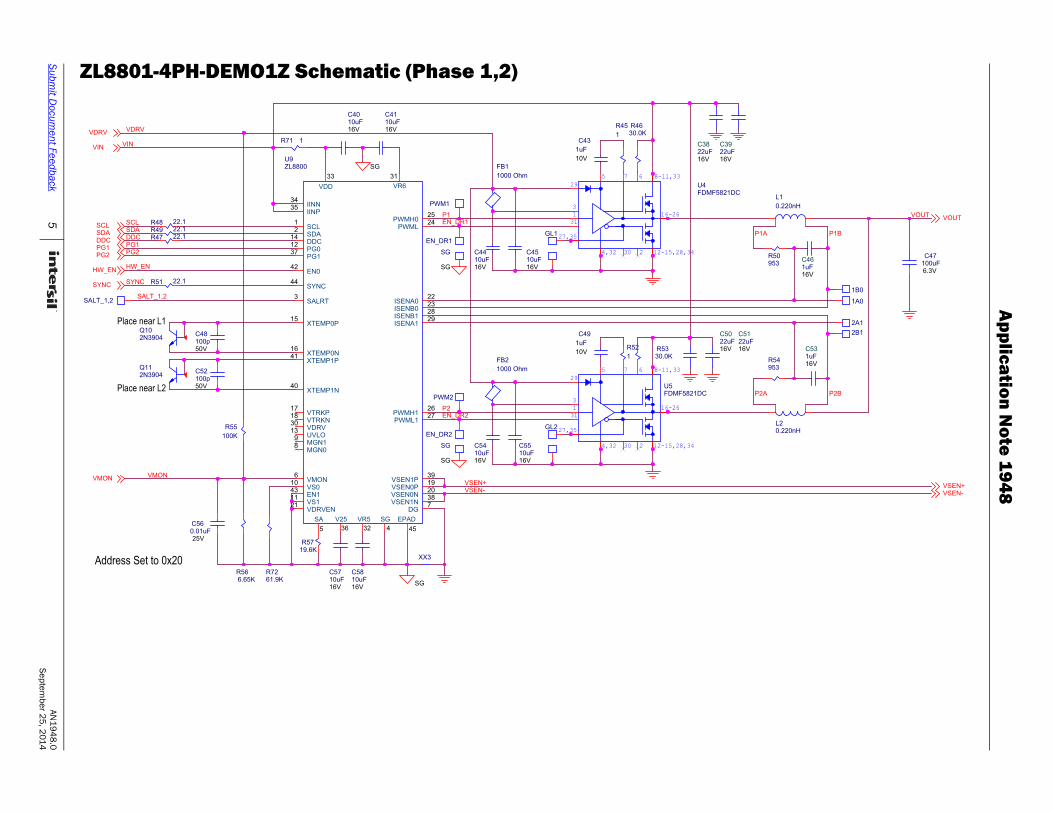
ZL8801-4PH-DEMO1Z Schematic (Phase 1,2)
Address Set to 0x20
Place near L1
Place near L2
VIN
DDC
SALT_1,2
SCLSDA
PG1PG2
SYNC
HW_EN
P2A P2B
P1A
VDRV
VSEN+VSEN-
VOUT
P1B
VMON
P1
P2
EN_DR1
EN_DR2
SG
SG
SG
SG
SDASCL
DDC
PG2PG1
HW_EN
SYNC
VDRV
VIN
VSEN+VSEN-
VOUT
VMON
1A0
FB2
1000 Ohm
R5719.6K
PWM2
Q112N3904
R71 1
1uF16V
C46
R52
1
PWM1
EN_DR1
U9ZL8800
SCL1
SDA2
SALRT3
SG
4
SA
5
VMON6
DG7
MGN08 MGN19
VS010
VS111
PG012
UVLO13
DDC14
XTEMP0P15
XTEMP0N16
VTRKP17
VTRKN18
VSEN0P19
VSEN0N20
VDRVEN21
ISENA022
ISENB023
PWML24PWMH025
PWMH126
PWML127
ISENB128
ISENA129
VDRV30
VR6
31
VR5
32
VDD
33
IINN34
IINP35
V25
36
PG137
VSEN1N38
VSEN1P39
XTEMP1N40
XTEMP1P41
EN042
EN143
SYNC44
EPAD
45
C4510uF16V
0.220nHL2
16V22uFC51
R48 22.1
R54953
C5410uF16V
R55
100K
2B1
1uF16V
C5316V22uFC50
R7261.9K
R49 22.1
C5810uF16V
2A1Q102N3904
XX3
SALT_1,2
R4630.0K
13
4,32
5 8-11,33
12-15,28,34
16-26
27,35
29
31
7 6
30 2
U4FDMF5821DC
C52100p50V
R566.65K
R51 22.1
FB1
1000 Ohm
EN_DR2
SG
GL2
16V22uFC39
R45
1
L1
0.220nH
C49
1uF
10V
C4410uF16V
GL1
1B0
13
4,32
5 8-11,33
12-15,28,34
16-26
27,35
29
31
7 6
30 2
U5FDMF5821DC
SG
C4010uF16V
R47 22.1
C5510uF16V
C560.01uF25V
R50953
C43
1uF
10V
C4110uF16V
R5330.0K
C5710uF16V
C47100uF6.3V
C48100p50V
16V22uFC38
Applicatio
n No
te 1948
6AN
1948
.0Septem
ber 25
, 2014
Subm
it Docum
ent Feedback
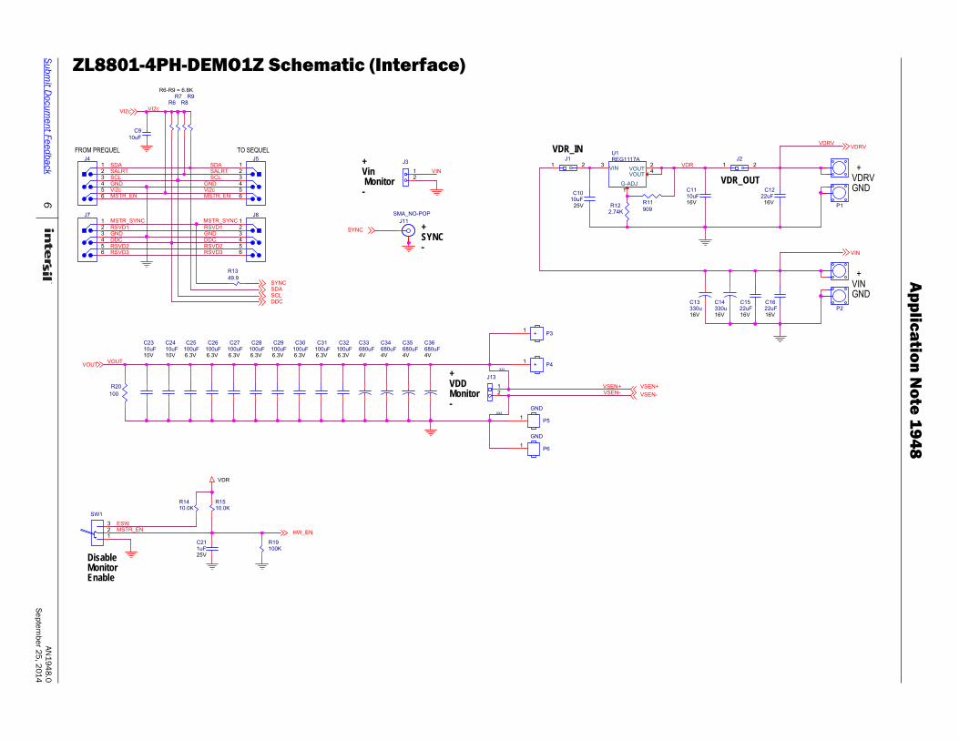
ZL8801-4PH-DEMO1Z Schematic (Interface)
+Vin Monitor-
Interface
DisableMonitorEnable
VDR_IN
VDR_OUT
+VINGND
+SYNC-
FROM PREQUEL TO SEQUEL
R6-R9 = 6.8K
+VDRVGND
+VDDMonitor-
VIN
VDRV
VDR
Vi2c
SCL
RSVD1 RSVD1
RSVD2 RSVD2RSVD3 RSVD3
GNDGND
GND
SALRTSDA
DDC
MSTR_SYNC
SALRT
GND
SDA
SCL
DDC
MSTR_SYNC
ESWMSTR_EN
MSTR_EN MSTR_ENVi2c
VOUT
VSEN+VSEN-
VI2c
VDR
VDRV
VIN
SYNC
DDC
SYNCSDASCL
HW_EN
VSEN+
VOUT
VSEN-
VI2c
Title
InterfaceTitle
InterfaceTitle
Interface
J4
2
4
6
1
3
5
R1410.0K
C1010uF
25V
C2310uF10V
C31100uF6.3V
R19100K
XX2
C211uF25V
J11
SMA_NO-POP
C1222uF
16V
P4+1
C9
10uF
C35680uF4V
R8
C30100uF6.3V
C26100uF6.3V
P2
C1110uF16V
C28100uF6.3V
C1622uF16V
C34680uF4V
P1
C29100uF6.3V
C13330u16V
C1522uF16V
R20
100
J121
R9
C25100uF6.3V
R6
R11
909
C33680uF4V
U1REG1117A
G-ADJ1
2VOUT
3VIN
4VOUT
P6
GND
1
R122.74K
SW1
123
J8
2
4
6
1
3
5
R13
49.9
P3+1
C32100uF6.3V
C27100uF6.3V
R7
J5
2
4
6
1
3
5
C14330u16V
C36680uF4V
C2410uF10V
R1510.0K
XX1
J7
2
4
6
1
3
5
J3
21
J13
21
P5
GND
1
J221

Applicatio
n No
te 1948
7AN
1948
.0Septem
ber 25
, 2014
Subm
it Docum
ent Feedback
ZL8801-4PH-DEMO1Z Schematic (Phase 3,4)
Address Set to 0x21
Place near L3
Place near L4
P3B
VIN
DDC
SALT_3,4
SCLSDA
PG3PG4
SYNC
P4A P4B
P3A
VOUT
VMON
HW_EN
P3
P4
VSEN+VSEN-
VDRV
EN_DR3
EN_DR4
SG
SG
SG
SG
VOUT
SDASCL
DDC
VSEN+VSEN-
PG4PG3
SYNC
VDRV
VIN
VMON
HW_EN
U6ZL8800
SCL1
SDA2
SALRT3
SG
4
SA
5
VMON6
DG7
MGN08
MGN19
VS010
VS111
PG012
UVLO13
DDC14
XTEMP0P15
XTEMP0N16
VTRKP17
VTRKN18
VSEN0P19
VSEN0N20
VDRVEN21
ISENA022
ISENB023
PWML24PWMH025
PWMH126
PWML127
ISENB128
ISENA129
VDRV30
VR6
31
VR5
32
VDD
33
IINN34 IINP35
V25
36
PG137
VSEN1N38
VSEN1P39
XTEMP1N40
XTEMP1P41
EN042
EN143
SYNC44
EPAD
45
1uF16V
C67
3A0
L3
0.220nH
SALT_3,4
C7810uF16V
C69
1uF
10V
13
4,32
5 8-11,33
12-15,28,34
16-26
27,35
29
31
7 6
30 2
U7FDMF5821DC
4B1
C64
1uF
10V
C6510uF16V
C7710uF16V
R64 22.1
Q122N3904
R62 22.1
R741 R59
30.0K
C6210uF16V
XX4
16V22uFC71
C6110uF16V
C7510uF16V
13
4,32
5 8-11,33
12-15,28,34
16-26
27,35
29
31
7 6
30 2
U8FDMF5821DC
3B0
Q132N3904
GL4
C68100p50V
FB3
1000 Ohm
EN_DR3
R63953
C6610uF16V
R65
1
R58
1
C760.01uF25V
EN_DR4
FB4
1000 Ohm
R6630.0K
R60 22.1
C7410uF16V
16V22uFC70
4A1
R6821.5K
SG
PWM3
R7361.9K
SG
0.220nHL4
R67953
GL3
16V22uFC60
1uF16V
C72
16V22uFC59
C63100p50V
PWM4
R61 22.1
Application Note 1948
8 AN1948.0September 25, 2014
Submit Document Feedback
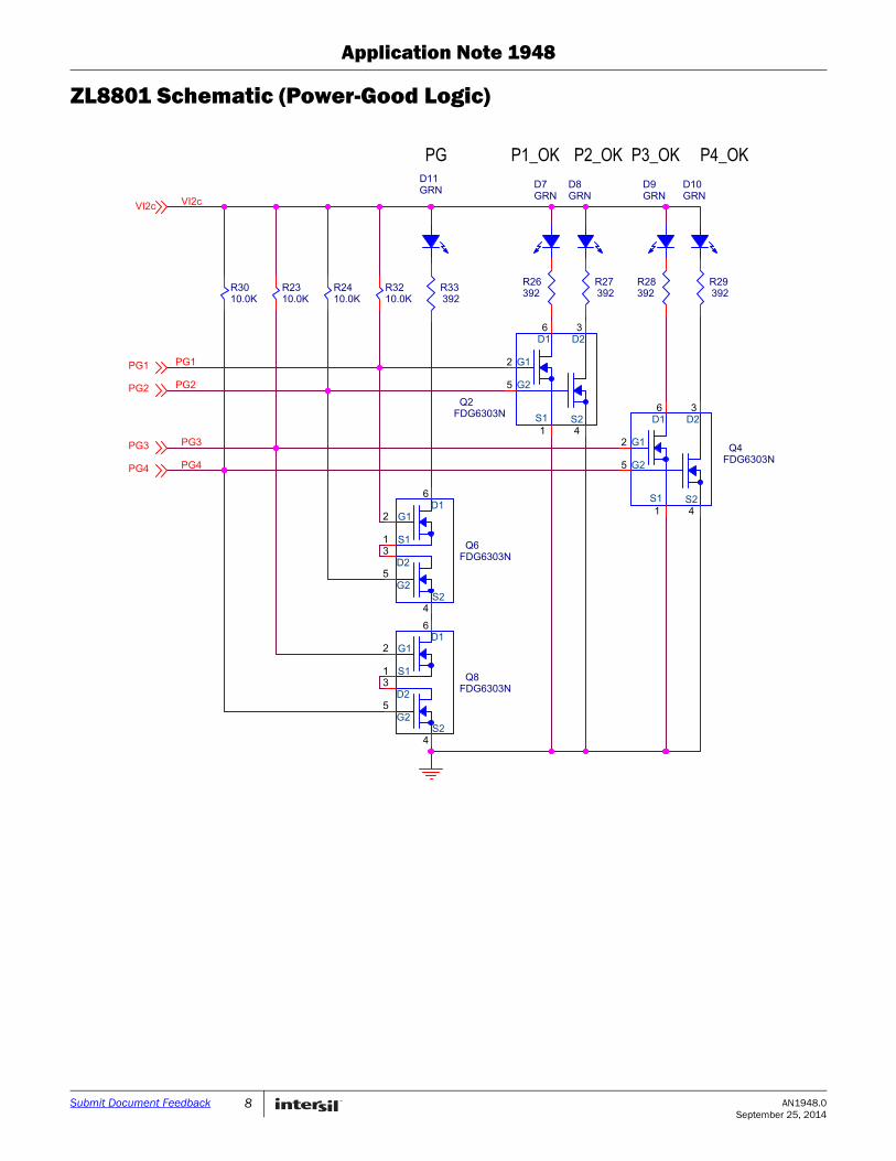
ZL8801 Schematic (Power-Good Logic)
PG P1_OK P4_OKP2_OK P3_OK
PG1
PG2
PG3
PG4
VI2c
PG1
PG2
PG3
PG4
VI2c
D11GRN
R2310.0K
D9GRN
R29392
Q4FDG6303N
S24
G25
D16
S1
1
G12
D23
R2410.0K
D7GRN
Q2FDG6303N
S24
G25
D16
S1
1
G12
D23
D10GRN
D8GRN
R26392
Q8FDG6303N
S24
D16
1 S1
2 G1
3D2
5G2
R3210.0K
R3010.0K
R33392
R27392
R28392
Q6FDG6303N
S24
D16
1 S1
2 G1
3D2
5G2

Application Note 1948
9 AN1948.0September 25, 2014
Submit Document Feedback
Bill of MaterialsITEM QTY REFERENCE VALUE TOL RATING TYPE PCB FOOTPRINT MANUFACTURER PART NUMBER
1 1 C9 10µF 10% 10V X7R SM0805 Taiyo Yuden LMK212B7106KG-TD
2 1 C10 10µF 10% 25V X5R SM1206 Panasonic - ECG ECJ-3YB1E106K
3 17 C11, C40, C41, C44, C45, C54, C55, C57, C58, C61, C62, C65, C66, C74, C75, C77,
C78
10µF 10% 16V X5R SM0805 TDK C2012X5R1C106K/0.85
4 11 C12, C15, C16, C38, C39, C50, C51, C59,
C60, C70, C71
22µF 20% 16V X5R SM1206 Murata GRM31CR61C226ME15L
5 2 C13, C14 330µF 20% 16V AL POLY SM_CAP_10.5X10.5_PXA_FLD United Chemi-Con APXA160ARA331MJC0G
6 1 C21 1µF 10% 25V X5R SM0603 Taiyo Yuden TMK107BJ105KA-T
7 2 C23, C24 10µF 10% 10V X7R SM0805 Murata GRM21BR71A106KE51L
8 9 C25, C26, C27, C28, C29, C30, C31, C32,
C47
100µF 6.3V X5R SM1210 Taiyo Yuden JMK325BJ107MY-T
9 4 C33, C34, C35, C36 680µF 20% 4V AL POLY SM7343_KEMET_T530_BC Kemet T530Y687M004ATE005
10 4 C43, C49, C64, C69 1µF 10% 10V X7R SM0603 Taiyo Yuden LMK107B7105KA-T
11 4 C46, C53, C67, C72 1µF 10% 16V X7R SM0603 TDK Corporation C1608X7R1C105K
12 4 C48, C52, C63, C68 100pF 5% 50V C0G SM0402_WSS MURATA GRM1555C1H101JZ01D
13 2 C56, C76 0.01µF 10% 25V X7R SM0402 Kemet C0402C103K3RACTU
14 5 D7, D8, D9, D10, D11 GRN 2V SM0805 Chicago Miniature CMD17-21VGC
15 4 FB1, FB2, FB3, FB4 1000Ω 150mA Ferrite SM0402 Taiyo Yuden BK1005HM102-T
16 4 J1, J2, J3, J13 2 POS VERT SIP2/100 Samtec TSW-102-07-L-S
17 2 J4, J7 HDR_3X2_RA RA HDRM3DUALRA100X100 SAMTEC TSW-103-08-T-D-RA
18 2 J5, J8 SKT_3X2_RA RA HDRF3DUALRA100X100 SAMTEC SSQ-103-02-T-D-RA
19 1 J11 SMA_NO-POP SMA_PCB_VJACK Emerson 142-9701-211
20 4 L1, L2, L3, L4 0.220nH 70 Inductor IND_SL3732_RXXXXX ITG SL3732_R22KHF
21 2 P1, P2 JACK 15A JACK Emerson 108-0740-001
22 2 P3, P4 CON_LUG
23 2 P5, P6 GND CON_LUG
24 4 Q2, Q4, Q6, Q8 FDG6303N 25V Dual N-Chan
SC70_6 Fairchild FDG6303N
25 4 Q10, Q11, Q12, Q13 2N3904 40V NPN SOT-23 ON SEMI MMBT3904LT1G
26 4 R6, R7, R8, R9 6.8k 1% 1/16W SM0402 Panasonic - ECG ERJ-2RKF6801X
27 1 R11 909 1% 100mW THK FILM SM0603 Panasonic - ECG ERJ-3EKF9090V
28 1 R12 2.74k 1% 100mW THK FILM SM0603 Panasonic - ECG ERJ-3EKF2741V
29 1 R13 49.9 1% 100mW THK FILM SM0402 Panasonic - ECG ERJ-2RKF49R9X
30 2 R14, R15 10.0k 1% 63mW THK FILM SM0402 Panasonic - ECG ERJ-2RKF1002X
31 1 R19 100k 1% 63mW THK FILM SM0402 Panasonic - ECG ERJ-2RKF1003X
32 1 R20 100 1% 100mW THK FILM SM0805 Panasonic - ECG ERJ-6ENF1000V
33 4 R23, R24, R30, R32 10.0k 1% 1/16W SM0402 Yageo RC0402FR-0710KL
34 5 R26, R27, R28, R29, R33
392 1% THK FILM SM0603 Panasonic - ECG ERJ-3EKF3920V

Application Note 1948
10 AN1948.0September 25, 2014
Submit Document Feedback
35 6 R45, R52, R58, R65, R71, R74
1 1% 1/16W SM0603 Panasonic - ECG ERJ-3RQF1R0V
36 4 R46, R53, R59, R66 30.0k 1% 1/16W SM0603 Panasonic - ECG ERJ-2GEJ303X
37 8 R47, R48, R49, R51, R60, R61, R62, R64
22.1 1% SM0402 Panasonic ERJ-2RKF22R1X
38 4 R50, R54, R63, R67 953 1% Resistor SM0603 Panasonic ERJ-3EKF9530V
39 1 R55 100k 1% 1/16W SM0402 Vishay/Dale CRCW0402100KFKED
40 1 R56 6.65k 1% 1/16W SM0402 Panasonic - ECG ERJ-2RKF6651X
41 1 R57 19.6k 1% 1/16W SM0402 Panasonic - ECG ERJ-2RKF1962X
42 1 R68 21.5k 1% 1/16W SM0402 Panasonic - ECG ERJ-2RKF2152X
43 2 R72, R73 61.9k 1% 1/16W SM0402 Panasonic - ECG ERJ-2RKF6192X
44 1 SW1 SW_SPDT PCBVERT
SW_TOG_ULTRAMIN_SPDT NKK G13AP-RO
45 1 U1 REG1117A SOT_223_1234 Texas Instruments REG1117A
46 4 U4, U5, U7, U8 FDMF5821DC 30V PQFN31_SPS_5X5_P5S Fairchild FDMF5821DC
47 2 U6, U9 ZL8800 MLF44_7X7_DP Intersil ZL8801
Bill of Materials (Continued)
ITEM QTY REFERENCE VALUE TOL RATING TYPE PCB FOOTPRINT MANUFACTURER PART NUMBER
Application Note 1948
11 AN1948.0September 25, 2014
Submit Document Feedback
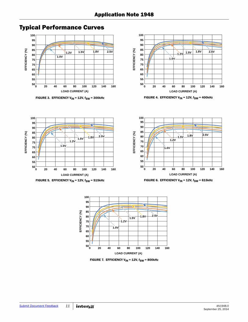
Typical Performance Curves
FIGURE 3. EFFICIENCY VIN = 12V, fSW = 300kHz FIGURE 4. EFFICIENCY VIN = 12V, fSW = 400kHz
FIGURE 5. EFFICIENCY VIN = 12V, fSW = 515kHz FIGURE 6. EFFICIENCY VIN = 12V, fSW = 615kHz
FIGURE 7. EFFICIENCY VIN = 12V, fSW = 800kHz
50
55
60
65
70
75
80
85
90
95
100
0 20 40 60 80 100 120 140 160
1.0V
1.2V 1.5V 1.8V 2.5V
LOAD CURRENT (A)
EF
FIC
IEN
CY
(%
)
50
55
60
65
70
75
80
85
90
95
100
0 20 40 60 80 100 120 140 160
1.0V
1.2V 1.5V 1.8V 2.5V
LOAD CURRENT (A)
EF
FIC
IEN
CY
(%
)
50
55
60
65
70
75
80
85
90
95
100
1.0V
1.2V1.5V 1.8V 2.5V
0 20 40 60 80 100 120 140 160
LOAD CURRENT (A)
EF
FIC
IEN
CY
(%
)
50
55
60
65
70
75
80
85
90
95
100
0 20 40 60 80 100 120 140 160
1.0V
1.2V1.5V 1.8V 2.5V
LOAD CURRENT (A)
EF
FIC
IEN
CY
(%
)
50
55
60
65
70
75
80
85
90
95
100
0 20 40 60 80 100 120 140 160
1.0V
1.2V1.5V 1.8V 2.5V
LOAD CURRENT (A)
EF
FIC
IEN
CY
(%
)

Application Note 1948
12 AN1948.0September 25, 2014
Submit Document Feedback
Measured Data
FIGURE 8. STATIC RIPPLE FIGURE 9. TURN-OFF RAMP
FIGURE 10. TURN-ON RAMP FIGURE 11. TRANSIENT RESPONSE
8mVP-P
VOUT
TYPICAL STATIC OUTPUT RIPPLE VOLTAGEVOUT = V, IOUT =50A, VIN = 12V, fSW = 515kHz
TYPICAL IMMEDIATE OFF TURN-ON RAMPVOUT = 1V, fSW = 515kHz, IOUT = 50A
VOUT = 1V
RESONANT ARTIFACT DUETO ELECTRONIC LOAD CABLE INDUCTANCE
VIN = 12V, VOUT = 1V, fSW = 515kHz, IOUT = 50ATYPICAL TURN-ON RAMP
MULTI_PHASE_RAMP_GAIN = 1
TUNE WITH MIN_VOUT_REGAN MULTI_PHASE_RAMP_GAINTO MINIMIZE
200mV START-UP ANOMALY
TRANSIENT RESPONSE IOUT = 20 TO 40A 10A/µsVIN = 12V, VOUT = 1V, fSW = 515kHzASCR GAIN = 275, RESIDUAL = 100
VOUT = 1V VP-P = 30mV
VSYNC

Application Note 1948
13 AN1948.0September 25, 2014
Submit Document Feedback
ZL8801-4PH-DEMO1Z Evaluation Board and Dongle
FIGURE 12. ZL8801-4PH-DEMO1Z CRITICAL COMPONENT LOCATION
KELVIN CONNECTED VOUTMEASUREMENT CONNECTION
ZL8801s
INSERT JUMPERS TO USEON BOARD VDRV REGULATORJ1, J2
CONNECT OTHER INTERSILDIGITAL POWER BOARDS HERE
EXTERNAL VDRV INPUTTYPICALLY USED FOR EFFICIENCYMEASUREMENTS. REMOVE J1, J2 AND CONNECT +5V EXTERNAL VDRV VOLTAGE
KELVIN CONNECTED VINMEASUREMENT CONNECTION
INPUT VOLTAGE CONNECTION
CONNECT USB TOPMBus DONGLE HERE
ENABLESWITCH
RAIL PGLAMP
OUTPUT VOLTAGE CONNECTION
FIGURE 13. USB TO PMBus DONGLE
USB CONNECTION TO
HOST COMPUTER
CONNECT TOZL8801-4PH-DEMO1Z J4DEMO BOARD
Application Note 1948
14 AN1948.0September 25, 2014
Submit Document Feedback
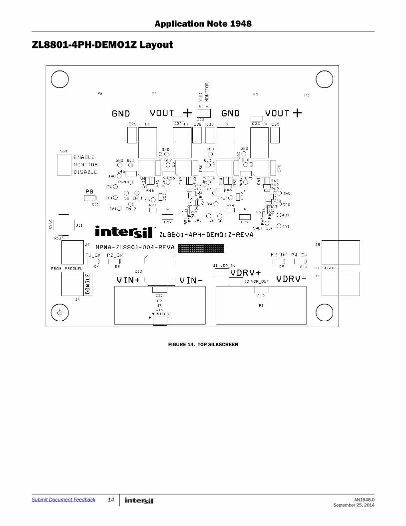
ZL8801-4PH-DEMO1Z Layout
FIGURE 14. TOP SILKSCREEN

Application Note 1948
15 AN1948.0September 25, 2014
Submit Document Feedback
FIGURE 15. TOP ETCH
ZL8801-4PH-DEMO1Z Layout (Continued)

Application Note 1948
16 AN1948.0September 25, 2014
Submit Document Feedback
FIGURE 16. INNER 1
ZL8801-4PH-DEMO1Z Layout (Continued)

Application Note 1948
17 AN1948.0September 25, 2014
Submit Document Feedback
FIGURE 17. INNER 2
ZL8801-4PH-DEMO1Z Layout (Continued)

Application Note 1948
18 AN1948.0September 25, 2014
Submit Document Feedback
FIGURE 18. INNER 3
ZL8801-4PH-DEMO1Z Layout (Continued)

Application Note 1948
19 AN1948.0September 25, 2014
Submit Document Feedback
FIGURE 19. INNER 4
ZL8801-4PH-DEMO1Z Layout (Continued)

Application Note 1948
20 AN1948.0September 25, 2014
Submit Document Feedback
FIGURE 20. INNER 5
ZL8801-4PH-DEMO1Z Layout (Continued)

Application Note 1948
21 AN1948.0September 25, 2014
Submit Document Feedback
FIGURE 21. INNER 6
ZL8801-4PH-DEMO1Z Layout (Continued)

Application Note 1948
22 AN1948.0September 25, 2014
Submit Document Feedback
FIGURE 22. BOTTOM ETCH
ZL8801-4PH-DEMO1Z Layout (Continued)

Application Note 1948
23
Intersil Corporation reserves the right to make changes in circuit design, software and/or specifications at any time without notice. Accordingly, the reader iscautioned to verify that the Application Note or Technical Brief is current before proceeding.
For information regarding Intersil Corporation and its products, see www.intersil.com
AN1948.0September 25, 2014
Submit Document Feedback
FIGURE 23. BOTTOM SILKSCREEN
ZL8801-4PH-DEMO1Z Layout (Continued)
Related Documents


