Z-SOURCE INVERTER FOR GRID-CONNECTED SOLAR PV APPLICATIONS A Project Report submitted by PAVAN VEMURI in partial fulfilment of requirements for the award of the degree of BACHELOR OF TECHNOLOGY DEPARTMENT OF ELECTRICAL ENGINEERING INDIAN INSTITUTE OF TECHNOLOGY MADRAS MAY 2021

Welcome message from author
This document is posted to help you gain knowledge. Please leave a comment to let me know what you think about it! Share it to your friends and learn new things together.
Transcript

Z-SOURCE INVERTER FOR GRID-CONNECTED
SOLAR PV APPLICATIONS
A Project Report
submitted by
PAVAN VEMURI
in partial fulfilment of requirements
for the award of the degree of
BACHELOR OF TECHNOLOGY
DEPARTMENT OF ELECTRICAL ENGINEERINGINDIAN INSTITUTE OF TECHNOLOGY MADRAS
MAY 2021

TABLE OF CONTENTS
LIST OF FIGURES 3
1 Motivation for ZSI 5
2 Topology 6
3 Working Principle 6
3.1 Equivalent Circuit . . . . . . . . . . . . . . . . . . . . . . . . . . . . . . . . . . . . 7
3.2 Voltage Derivation . . . . . . . . . . . . . . . . . . . . . . . . . . . . . . . . . . . 8
4 Sine-triangle Implementation 10
4.1 Direct Implementation . . . . . . . . . . . . . . . . . . . . . . . . . . . . . . . . . 10
4.2 Dividing shoot-through equally . . . . . . . . . . . . . . . . . . . . . . . . . . . . . 11
5 Inductor and Capacitor Ripple 13
5.1 Maximum Ripple Instant . . . . . . . . . . . . . . . . . . . . . . . . . . . . . . . . 13
5.2 Inductor Ripple . . . . . . . . . . . . . . . . . . . . . . . . . . . . . . . . . . . . . 14
5.3 Capacitor Ripple . . . . . . . . . . . . . . . . . . . . . . . . . . . . . . . . . . . . 15
6 DCM Possibility in ZSI 15
7 An Improved ZSI Topology 16
7.1 Disadvantages of traditional ZSI . . . . . . . . . . . . . . . . . . . . . . . . . . . . 16
7.2 Alternate Topologies . . . . . . . . . . . . . . . . . . . . . . . . . . . . . . . . . . 16
7.3 Improved Topology . . . . . . . . . . . . . . . . . . . . . . . . . . . . . . . . . . . 17
7.3.1 Voltage Derivation . . . . . . . . . . . . . . . . . . . . . . . . . . . . . . . 18
8 Solar array characteristics and topology 18
1

8.1 Solar panel characteristics . . . . . . . . . . . . . . . . . . . . . . . . . . . . . . . 18
8.2 Solar array topology . . . . . . . . . . . . . . . . . . . . . . . . . . . . . . . . . . 19
8.3 Three phase vs single phase grid-connected ZSI . . . . . . . . . . . . . . . . . . . . 20
9 Control Scheme 21
9.1 MPPT . . . . . . . . . . . . . . . . . . . . . . . . . . . . . . . . . . . . . . . . . . 21
9.2 Inverter Current Control [6] . . . . . . . . . . . . . . . . . . . . . . . . . . . . . . . 21
10 Simulation Results 21
10.1 Three phase ZSI with R-load . . . . . . . . . . . . . . . . . . . . . . . . . . . . . . 21
10.2 Improved ZSI with R-load . . . . . . . . . . . . . . . . . . . . . . . . . . . . . . . 23
10.3 Three phase grid-connected solar ZSI (openloop) . . . . . . . . . . . . . . . . . . . 23
11 Conclusion 24
REFERENCES 25
2

LIST OF FIGURES
1 Traditional Inverters . . . . . . . . . . . . . . . . . . . . . . . . . . . . . . . . . . . 5
2 ZSI Topology . . . . . . . . . . . . . . . . . . . . . . . . . . . . . . . . . . . . . . 6
3 ZSI Equivalent Circuit . . . . . . . . . . . . . . . . . . . . . . . . . . . . . . . . . 7
4 Equivalent circuits in the two states . . . . . . . . . . . . . . . . . . . . . . . . . . . 7
5 Buck-boost characteristics of ZSI . . . . . . . . . . . . . . . . . . . . . . . . . . . . 9
6 Inputs of the inverter switches . . . . . . . . . . . . . . . . . . . . . . . . . . . . . 10
7 Equal shoot-through division . . . . . . . . . . . . . . . . . . . . . . . . . . . . . . 11
8 Effective 6x switching frequency . . . . . . . . . . . . . . . . . . . . . . . . . . . . 13
9 Maximum time between two shoot-through’s . . . . . . . . . . . . . . . . . . . . . 13
10 Maximum ripple cycle . . . . . . . . . . . . . . . . . . . . . . . . . . . . . . . . . 14
11 Third possible state in DCM . . . . . . . . . . . . . . . . . . . . . . . . . . . . . . 15
12 Equivalent circuit on start-up . . . . . . . . . . . . . . . . . . . . . . . . . . . . . . 16
13 Quasi-ZSI . . . . . . . . . . . . . . . . . . . . . . . . . . . . . . . . . . . . . . . . 17
14 No LC resonance ZSI . . . . . . . . . . . . . . . . . . . . . . . . . . . . . . . . . . 17
15 Equivalent circuits in the two states . . . . . . . . . . . . . . . . . . . . . . . . . . . 18
16 Single diode model of a PV panel . . . . . . . . . . . . . . . . . . . . . . . . . . . 19
17 Typical solar panel characteristics . . . . . . . . . . . . . . . . . . . . . . . . . . . 19
18 Problems with single-phase ZSI . . . . . . . . . . . . . . . . . . . . . . . . . . . . 20
19 Three phase ZSI with R-load . . . . . . . . . . . . . . . . . . . . . . . . . . . . . . 21
20 Simulation Plots . . . . . . . . . . . . . . . . . . . . . . . . . . . . . . . . . . . . . 22
21 Inductor current and Capacitor voltage in the maximum ripple instant . . . . . . . . 22
22 Three phase ZSI with R-load . . . . . . . . . . . . . . . . . . . . . . . . . . . . . . 23
23 Improved ZSI Simulation . . . . . . . . . . . . . . . . . . . . . . . . . . . . . . . . 23
24 Simulation schematic . . . . . . . . . . . . . . . . . . . . . . . . . . . . . . . . . . 23
3

25 Solar array characteristics . . . . . . . . . . . . . . . . . . . . . . . . . . . . . . . . 24
26 Simulation Plots . . . . . . . . . . . . . . . . . . . . . . . . . . . . . . . . . . . . . 24
4

1 Motivation for ZSI
(a) Volatge Source Inverter (b) Current Source Inverter
Figure 1: Traditional Inverters
The Voltage Source Inverter (VSI) is the simplest of the inverters with a DC bus(or an equivalent
source) connected to a three-phase bridge. VSI is a buck inverter as the output AC peak voltage
is always lesser than the DC bus voltage. In applications where higher AC voltage is required, an
additional boost converter is required on the DC side to feed the inverter with a boosted DC source.
VSI also needs sufficient dead time , when switching between the top switch and bottom switch of
a phase-leg, to avoid shoot-through which may short the DC bus leading to a high current flowing
through that leg. This dead time could potentially cause waveform distortion.
Current Source Inverter (CSI) on the other hand has a current source at its input (or equivalently
a DC voltage source in series with an inductor). CSI is a boost inverter as the output AC voltage is
always higher than the DC voltage which is feeding the inductor. In CSI at least one of the devices of
each leg should be ON at any point of time to avoid any open circuit of the source inductor. Hence CSI
needs overlap time while switching the devices which also causes waveform distortion.
Neither VSI nor CSI can perform buck-boost operation. The main circuit of VSI consists a power
switch with an anti-parallel diode for bi-directional current flow. CSI’s switches consist of a power
switch with a series diode to block reverse voltage. Hence the main circuits of VSI and CSI are design
specific and cannot be interchanged.
5

Voltage Source Inverter Current Source Inverter
Buck inverter Boost inverter
Distortion due to dead-time Distortion due to overlap-time
Output LC filterSeries diode with the switches to
prevent reverse voltage
Buck-boost inversion is not possible
Main circuits are not interchangeable between VSI and CSI
Table 1: Disadvantages of conventional inverters
2 Topology
Figure 2: ZSI Topology
The Z-source Inverter (ZSI) [1] aims to standardize the inverter main circuit irrespective of a voltage
source or current source at the input. ZSI uses an impedance network between the source and the
inverter main circuit. This solves the major problem of the need for dead time or overlap time because
any open circuit or short circuit in the main circuit does not directly effect the DC source as it is isolated
from the main circuit through the Z-network. This impedance network helps to store energy and boost
the DC side voltage to a higher value.
3 Working Principle
Compared to VSI, ZSI has an additional zero-state vector which is the shoot-through zero state. Boost
feature of ZSI is obtained using the shoot-through zero state. Voltage is boosted when the shoot-
through zero state is implemented instead of the conventional zero state. Shoot-through can be achieved
by shorting at least one of the legs of the inverter, which can be done in seven ways.
6

During transient, the higher energy drawn from the source is stored in the inductor and is then trans-
ferred to the capacitor to build up the voltage. Inductor energy builds up during non shoot-through state
and is transferred to the capacitor during shoot-through state. The shoot-through state is equivalently
forming two LC circuits with L1;C1 and L2;C2. Hence the energy transfer from L to C happens
through LC resonance.
3.1 Equivalent Circuit
Figure 3: ZSI Equivalent Circuit
(a) Non shoot-through (b) Shoot-through
Figure 4: Equivalent circuits in the two states
Figure 3 shows the equivalent circuit of ZSI with a DC voltage source at the input. The voltage
across the inverter is vi and the current drawn by the load is ii. During non shoot-through, the main
circuit is modeled as a current sink, so that even if no current is drawn by the load, the the voltage
across the main circuit could still be non-zero (Figure 4a). Whereas during shoot-through, the main
circuit is shorted by at least one of the legs, so the voltage across it is zero (Figure 4b). The source
diode will be OFF during the shoot-through stage as vd > V0. This is because the voltage across the
capacitors VC is at least V0 and the drop across the inductor would make vd = (VC + vL) > V0
7

3.2 Voltage Derivation
For simplicity, assume L1 = L2 and C1 = C2. Now the impedance network becomes symmetric,
vL1 = vL2 = vL and VC1 = VC2 = VC
Let Ts be the switching period of the inverter. Let T1 and T0 be the duration for which the inverter
is in non shoot-through and shoot-through states respectively in one switching period. These quantities
can be related as,
Ts = T0 + T1
During non shoot-through, from Figure 4a,
vL = V0 − VC ; vd = V0; vi = 2VC − V0
During shoot-through, from Figure 4b,
vL = VC ; vd = 2VC ; vi = 0
By applying volt-sec balance to the inductors,
< vL >= 0;
(V0 − VC).T1 + VC .T0 = 0;
VC =T1
T1 − T0.V0
Voltage across the inverter during non shoot-through,
vi = 2VC − V0 = Ts
T1−T0.V0 = B.V0;
B = Ts
T1−T0= 1
1−2T0Ts
≥ 1
Maximum boost factor depends on the maximum time available for shoot-through. For a given
modulation index M , output high duration = M.Ts. Maximum time available for an active state = T1.
M.Ts ≤ T1;
8

M.Ts ≤ Ts − T0;
T0 ≤ (1−M).Ts
Bmax =1
2M − 1
For a given modulation indexM and given voltage Vinv across the inverter, output AC voltage peak,
v̂ac−max = M.Vinv
2
In maximum boost operation, Vinv = V0
2M−1 ;
v̂ac−max =M
2M − 1.V02
Figure 5: Buck-boost characteristics of ZSI
In buck mode v̂ac0.5Vdc
= M and in maximum boost mode v̂ac0.5Vdc
= M2M−1
For boost operation, it is always better to operate close to the maximum boost line for the efficient
use of the Z-network. In any operating point under the maximum boost line, we would be boosting the
DC voltage to a higher value and operating at a lower modulation index compared to the maximum
boost point for the required AC peak voltage.
9

4 Sine-triangle Implementation
4.1 Direct Implementation
(a) Traditional SPWM (b) SPWM with shoot-through
Figure 6: Inputs of the inverter switches
In Figure 6, va, vb, vc denote the values of the 3-phase modulating signals at a particular instant.
Sap, Sbp, Scp are the corresponding inputs to the top switches. San, Sbn, Scn are the corresponding in-
puts to the bottom switches of the inverter.
In Figure 6a, the regions marked in orange denote the traditional zero-state of the inverter(V000, V111).
In the direct implementation, the shoot-through zero state is implemented during the traditional zero-
state by shorting atleast one of the legs. Compared to traditional SPWM, this shoot-trough implemen-
tation needs to tweak only two of the six wave-forms of the control voltages in every cycle. Hence it
is very efficient in terms of the logic used for its generation.
To achieve a shoot-through period of T0 = D.Ts, we have to identify the max and min of va, vb, vc
and increase the max value by D for the corresponding top switch and reduce the min value by D for
the corresponding bottom switch. Doing this, we get a shoot-through time of D.Ts
2from each of the
two zero-states(V000, V111). Note that the switching frequency of the switches remains the same.
In the above instant, va is the maximum and vc is the minimum. So we have to effectively generate
SPWM with va +D, vb, vc for top switches and va, vb, vc −D for the bottom switches. Corresponding
plot is shown in Figure 6b
10

4.2 Dividing shoot-through equally
Figure 7: Equal shoot-through division
Figure 7 shows the implementation by dividing the shoot-through time equally among the three legs of
the inverter. Here also the switching frequency of the inverter doesn’t change.
Shoot-through state is introduced at every toggling of the legs. Each leg toggles twice in a period
and there are three legs, so there are six toggles happening in one period. A shoot-through duration ofD.Ts
6is introduced at every toggle of the legs to get an overall shoot-through duration of D.Ts from the
entire period.
The implementation logic is slightly complicated because the toggling caused by mid is not close
to a traditional zero state. So to implement shoot-through for mid transition, zero state time has to be
borrowed from either max or min toggles, whichever has same sign as mid. This choice of max or
min is made to avoid any overlap of shoot-through’s of any of the six toggles. Borrowing zero state
frommax orminwith same sign asmid ensures non overlapping shoot-through’s as the shoot-through
time is borrowed from the same traditional zero state i.e., either V000 or V111.
This implementation gives the advantage of having an effective switching frequency of 6x between
shoot-through and non shoot-through states, hence smaller L and C are needed to achieve a given
ripple specification.
11

MATLAB code for the equal shoot-through implementation is given below:
%[mR,mY,mB] are the modulating signals at an instant
%M - (Modulation index)
%[r,y,b] and [r_,y_,b_] are the output modulating signals for the top and ...
bottom switches
function [b,b_,y,y_,r,r_] = transform(mR,mY,mB,M)
inp = [mR,mY,mB];
out = [mR,mY,mB];
out_ = [mR,mY,mB];
m0 = 2*(1-M)/3;
[ma,amax] = max(inp);
[mi,amin] = min(inp);
if (inp(6-amax-amin) > 0)
out_(amin) = inp(amin) - m0;
out(6-amax-amin) = inp(6-amax-amin) + m0;
out(amax) = inp(amax) + 2*m0;
out_(amax) = inp(amax) + m0;
else
out(amax) = inp(amax) + m0;
out_(6-amax-amin) = inp(6-amax-amin) - m0;
out_(amin) = inp(amin) - 2*m0;
out(amin) = inp(amin) - m0;
end
b = out(3); b_ = out_(3);
y = out(2); y_ = out_(2);
r = out(1); r_ = out_(1);
12

Given below is a simulation plot of the voltage across the inverter depicting the shoot-through
happening six times in one period -
Figure 8: Effective 6x switching frequency
5 Inductor and Capacitor Ripple
5.1 Maximum Ripple Instant
(a) 3-phase modulating signals (b) Tmax occurrence
Figure 9: Maximum time between two shoot-through’s
To find the accurate ripple expressions, we have to identify the period when the inverter stays in a
particular state(shoot-through or non shoot-through) for the longest time.
Suppose max,mid,min is the descending order of modulating voltages in a particular cycle, leg
corresponding to min switches first, then mid, then max. So to find the maximum time between two
shoot-through’s, we have to find the maximum possible value of (max-mid) or (mid-min). From Figure
9a, the maximum value happens to be 3M2
and occurs when [max=M ; mid=min=-0.5M] or [min=-M ;
mid=max=0.5M]
The corresponding maximum time between shoot-through’s (Figure 9b) is given by,
13
Tmax =3.M.Ts
8
Figure 10: Maximum ripple cycle
During the maximum ripple cycle, Tmax occurs twice with some shoot-through states in between
(Figure 10). The corresponding duration of shoot-through and non shoot-through are given by,
Tnst = 2 ∗ Tmax + (1−M).Ts
6;
Tnst =(7M + 2).Ts
12
Tst =(1−M).Ts
3
The maximum ripple occurs as the resultant of Tnst and Tst
5.2 Inductor Ripple
During non shoot-through, vL1 = Vg − VC = − 1−M2M−1Vg
During shoot-through, vL2 = VC = M2M−1Vg
∆ipk−pk = vL1.Tnst+vL2.Tst
L
∆ipk−pk =(3M + 2).(1−M)
12.(2M − 1)
Vg.TsL
14

5.3 Capacitor Ripple
During shoot-through, iC2 = IL
By amp-sec balance, during non shoot-through, iC1 = −1−MM
IL
∆vpk−pk = iC1.Tnst+iC2.Tst
L
∆vpk−pk =(3M + 2).(1−M)
12M
IL.TsC
Capacitor ripple has been obtained as a function of IL, which in-turn depends on the load. In the
ideal case of zero losses, Pg = Pload and from the ZSI topology, < ig >= IL.
=⇒ Vg.IL = Pload
IL =Pload
Vg
6 DCM Possibility in ZSI
Figure 11: Third possible state in DCM
Figure 4a and Figure 4b show the equivalent circuits during non shoot-through and shoot-through. The
main circuit switches are in our control to decide the state of the ZSI. The assumption is that during non
shoot-through, the inductor voltage is non-zero and is high enough to turn on the source diode. This
assumption fails in DCM when the inductor current saturates to zero and the voltage drop across the
inductor is zero. Since Vc > V0, the source diode turns off and the capacitors supply the required load
current. The equivalent circuit of the third possible state in ZSI is given in Figure 11. The equations
governing this state are:
vL = 0 ; vi = Vc ; iC = ii
15
7 An Improved ZSI Topology
7.1 Disadvantages of traditional ZSI
1. Switching current drawn from the source:Since the source diode is OFF during shoot-through, the current drawn from the source is pulsat-ing. This can be avoided by having a capacitor in parallel with the DC voltage source to absorbthe ripples.
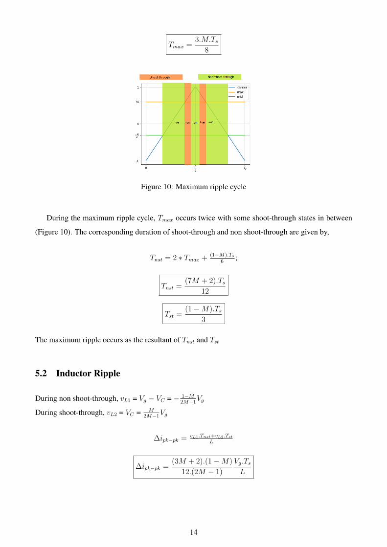
2. Inrush current due to LC-resonance:Inrush current is observed due to a combined effect of LC-resonance and shoot-through. Duringstartup when the capacitors are charging up, the voltage across them is not high enough to turnOFF the source diode during shoot-through, making the circuit equivalently an LC circuit.Shoot-through inrush can be eliminated by doing soft-start i.e., gradually increasing the shoot-through time from zero to the desired value.
Figure 12: Equivalent circuit on start-up
Since load current is initially zero and the capacitors are not charged up, the circuit behaves asan LC oscillator for a period of π
√LC. After that the inductor current cannot go negative as the
source diode turns OFF and there is no further oscillation. As shown in the Figure 12, assuming
the main circuit is OFF initially, iL = 2Vg
√CLsin( t√
LC), for 0 < t < π
√LC. So we observe a
current peak of Vg√
CL
on startup.
This inrush is not a problem with a solar array at the input because the current that the solararray can provide is limited by its short-circuit current which is very low compared to the LCresonance peak current.
3. High capacitor stress:The steady state voltage across the capacitors is given by VC = M
2M−1Vg (M>0.5), which is muchhigher than Vg requiring bulky capacitors.
7.2 Alternate Topologies
1. Quasi ZSI [2]: smooth source current
16

Figure 13: Quasi-ZSI
Quasi-ZSI’s topology has an inductor in series with the DC volatge source to have continuoussource current.
2. Swapping diode and main circuit: no LC resonance and reduced capacitor stress
Figure 14: No LC resonance ZSI
7.3 Improved Topology
The topology in Figure 14 eliminates LC resonance and makes the inverter compact by reducing ca-
pacitor stress [3].
LC resonance is eliminated because the source-LC path completes through the inverter. Direct source-
LC path is established only during shoot-through, which is anyways being soft-started. The soft-start
period allows the LC network to charge up slowly instead of resonating.
17

7.3.1 Voltage Derivation
(a) Non shoot-throughvL = −VC
vi = Vg + 2VC
(b) Shoot-thoroughvL = Vg + VC
iC = −IL
Figure 15: Equivalent circuits in the two states
< vL >= 0 =⇒ VC = Vg .T0
T1−T0
VC =1−M2M − 1
Vg
The above derived VC is less than that in the traditional ZSI (VC = M2M−1Vg), as M > 0.5 for boost
operation.
Voltage across the inverter, vi = Vg + 2VC = 12M−1Vg, which is same as in the traditional ZSI. The
voltages across the inductor and the currents in the capacitor during shoot-through and non shoot-
through are the same. So, the ripple quantities also do not change.
8 Solar array characteristics and topology
8.1 Solar panel characteristics
To a first order, solar cell can be modeled as a current source in parallel with a diode [4]. The current
source signifies the electron-hole pairs generated from the depletion region when light falls on it and
the diode signifies the recombination of few of the generated pairs due the forward voltage across the
solar cell, which itself is a special pn-junction diode.
A practical solar panel, which is obtained from a series-parallel combination of solar cells, can be
modeled with some series and parallel resistance along with the effective current source and diode.
18

Figure 16: Single diode model of a PV panel
The equation governing the above model is given by,
I = Ipv − Id0[exp(V+IRs
a.Vt)− 1
]− V+IRs
Rp
Vt = NskTq
, when Ns cells are in series and a is the diode idelaity factor( ≈ 1). The value of Ipv is
a function of solar radiation.
Typical I-V and Power-Voltage characteristics of a solar panel are given below:
(a) IV characteristics at different radiations (b) Power-V characteristics at a particular radiation
Figure 17: Typical solar panel characteristics
As shown in the power-voltage characteristics, there is a particular voltage of operation at which
the output power is maximum. We need to operate close to the maximum power point for efficient use
of the panels. This is called Maximum Power Point Tracking (MPPT).
8.2 Solar array topology
A typical solar panel of 2m*1m dimensions has MPP at ∼320Wp @ ∼40Vp. Assuming a 16m2
rooftop area, 8 such panels can be used to get ∼2.5KWp power
All panels in series: Advantage is that the boost factor will be lower as the DC bus voltage is higher.
19
But the disadvantage is that partial shadowing of one of the panel limits the current in the whole array
leading to a lesser output power.
Hence a 4*2 series-parallel topology is optimal.
8.3 Three phase vs single phase grid-connected ZSI
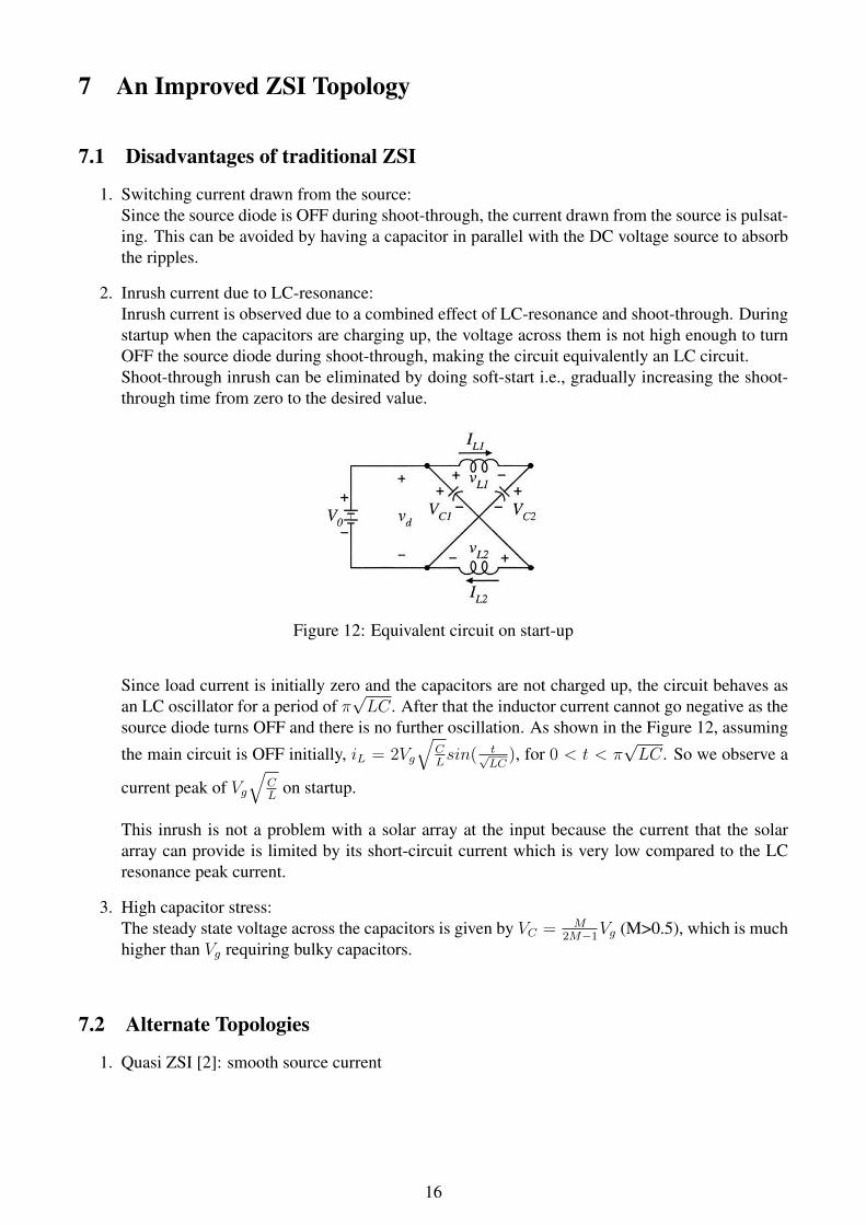
To keep the inverter hardware minimal, isolation transformer is tried to be avoided in the design.
Problem with transformer-less single phase grid-connected ZSI:
• Potential Induced Degradation(PID) in full-bridge topology. Here the neutral of the grid has tobe connected to a switching node. Considering neutral as a universal ground, all nodes in theZSI, including the solar panel terminals, will be switching wrt neutral. This makes the parasiticcapacitance between the solar panels and earth active through the frame of the panels. This notonly increases losses but also degrades the panels over time.
• Half-bridge topology is not feasible as the DC side is disconnected from the grid during shoot-through state. So neutral cannot be connected to the mid voltage of the DC side. Theoreticallythis is possible with an infinite capacitance on DC side, as an infinite capacitance need not satisfyamp-sec balance.
(a) Resistive parasitic between the panel andearth
(b) Theoretical half-bridge topology
Figure 18: Problems with single-phase ZSI
Though single-phase supplies are common in households, three-phase ZSI has been chosen, for the
above short-comings of single-phase ZSI. Three phase system gives the advantage of avoiding neutral
connection.
20

9 Control Scheme
9.1 MPPT
MPPT can be implemented by a simple perturb and observe control [5] on the reference current pumped
into the grid. The volatge and current from the solar array is sampled at a rate slower than the switching
frequency. Let ∆iprev be the MPPT output and Pprev be the measured power in the previous instant
and Pcurr be the power measured now. The sign of the present output ∆icurr should be the sign of
(Pcurr − Pprev) ∗ ∆iprev, i.e., if in the previous instant reference current has been increased but the
power output has reduced it would imply that we are on the falling side of the power hill, so the
reference needs to be reduced. Similarly for the other three cases, the reference current is increased or
decreased accordingly.
9.2 Inverter Current Control [6]
The three phase grid-side currents are measured and converted to d-q quantities using the Clarke trans-
formation. The d-reference for current is given by the MPPT and the q-reference is set to zero to deliver
power at unity power factor. The compensator takes the grid-side dq current values as inputs and gives
out the required voltage and phase required on the inverter side output. Based on the compensator
output and the DC volatge of solar array, required modulation index for maximum boost operation
is calculated and fed to the switches. The ZSI is operated in maximum boost mode for the efficient
utilization of the Z-network.
10 Simulation Results
10.1 Three phase ZSI with R-load
Figure 19: Three phase ZSI with R-load
21

Functionality of ZSI has been verified by simulation with a 150V DC source and three phase R load.
The ZSI has been operated in maximum boost mode at a modulation index of 0.7 and a switching
frequency of 10kHz. Theoretical boosted voltage is given by Vdc
2M−1 = 375V and the simulated value
matches the expected one. Shoot-through has been implemented as illustrated in Section 4.2.
(a) Inverter Voltage switching between 375V and 0Vduring non shoot-through and shoot-through statesrespectively
(b) Three phase voltages with three levels
Figure 20: Simulation Plots
Inductor and capacitor values used are 1mH and 1mF respectively. The ripple quantities as calcu-
lated in Section 5 are found to be matching with the simulated value.
Calculated ripple values are - (Vg = 150 , M = 0.7 , Ts = 10−4)
∆ipk−pk = (3M+2).(1−M)12.(2M−1)
Vg .Ts
L= 3.84A ; ∆vpk−pk = (3M+2).(1−M)
12MIL.Ts
C= 0.53V
Figure 21: Inductor current and Capacitor voltage in the maximum ripple instant
Calculated Simulated
∆ipk−pk(A) 3.84 3.82
∆vpk−pk(V) 0.53 0.41
Table 2: Ripple quantities comparison
22

10.2 Improved ZSI with R-load
Figure 22: Three phase ZSI with R-load
Simulation of the improved ZSI is done with same component values as above except that the source
diode and main circuit are interchanged. The current peak due to resonance has become as low as
15A, which is much below the operating point of 75A. The capacitor voltage is 111V, which in case of
traditional ZSI was 262V, giving an improvement of M1−M = 0.7
1−0.7 = 2.33 in the capacitor stress. The
inductor and capacitor ripple quantities have also been verified to be the same as with traditional ZSI.
(a) LC resonance peak being only 15A (b) Inductor and capacitor ripple being the same as tra-ditional ZSI
Figure 23: Improved ZSI Simulation
10.3 Three phase grid-connected solar ZSI (openloop)
Figure 24: Simulation schematic
23

A solar array with 8 panels connected in 4-series, 2-parallel topology has been used as the input. The
IV and PV characteristics of the array at 1000 W/m2 radiation @ 35 ◦ C ambient temperature is given
below -
Figure 25: Solar array characteristics
The modulation index has been adjusted so that the output power is close to the MPP. The ZSI is
operated at 0.6 modulation index which gave an output power of 2192W.
The solar array in steady state is operated @ 156V , 14.4 A. Theoretical boosted voltage is given byVdc
2M−1 = 780V , but the simulated value is found to be 1066V which is because of the inductors which
are connected between the inverter and the grid. The 5-level phase voltage is because the voltages are
referred to the neutral of the grid and not the mid-point of the DC side.
(a) Inverter Voltage switching from 0V to 1066V (b) Three phase voltages with five levels
Figure 26: Simulation Plots
11 Conclusion
The Z-source inverter uses an impedance network between the source and main circuit, which provides
some unique features compared to the traditional VSI and CSI. It has been verified from simulations
that ZSI overcomes the shortcomings of conventional inverters. ZSI can effectively replace all the sys-
tems which use a boost converter and VSI pair to achieve boosted inversion.
24

ZSI can also make household PV systems compact by avoiding a boost converter and also making
the controls minimal. The current control for grid-connected ZSI has to be done carefully as the shoot-
through implementation needs the present modulation index along with the modulating wave-forms
with both of them having same delay, and delay skew might vary the ZSI transfer function.
REFERENCES
[1] Fang Zheng Peng, "Z-Source Inverter", 2003
[2] Yuan Li1, Joel Anderson, Fang Z. Peng, Dichen Liu, "Quasi-Z-Source Inverter for Photovoltaic
Power Generation Systems", 2009
[3] Yu Tang, Shaojun Xie, Chaohua Zhang, Zegang Xu, "Improved Z-Source Inverter With Reduced
Z-Source Capacitor Voltage Stress and Soft-Start Capability", 2009
[4] Marcelo Gradella Villalva, Jonas Rafael Gazoli, Ernesto Ruppert Filho, "Comprehensive Approach
to Modeling and Simulation of Photovoltaic Arrays", 2009
[5] Richard Badin, Yi Huang, Fang Z. Peng, Heung-Geun Kim, "Grid Interconnected Z-Source PV
System", 2007
[6] Arun Karuppaswamy B, "Synchronous Reference Frame Strategy based STATCOM for Reactive
and Harmonic Current Compensation", M.Tech Thesis, NIT Calicut 2007
25
Related Documents