_____________________________________________________________________________ General Standards Corporation Ph:(256)880-8787 FAX:(256)880-8788 Email: [email protected] MAN-XMC-16AI32SSC1M Rev: 021417 XMC-16AI32SSC1M 32-CHANNEL DIFFERENTIAL 16-Bit, SIMULTANEOUS SAMPLING, XMC ANALOG INPUT BOARD With 1MSPS Sample Rate per Channel, Low Latency Access, and Time Tagging _______________________ REFERENCE MANUAL --- PRELIMINARY ---

Welcome message from author
This document is posted to help you gain knowledge. Please leave a comment to let me know what you think about it! Share it to your friends and learn new things together.
Transcript

_____________________________________________________________________________ General Standards Corporation Ph:(256)880-8787 FAX:(256)880-8788 Email: [email protected]
MAN-XMC-16AI32SSC1M
Rev: 021417
XMC-16AI32SSC1M
32-CHANNEL DIFFERENTIAL 16-Bit,
SIMULTANEOUS SAMPLING, XMC ANALOG INPUT BOARD
With 1MSPS Sample Rate per Channel, Low Latency Access, and Time Tagging
_______________________
REFERENCE MANUAL
--- PRELIMINARY ---

XMC-16AI32SSC1M Preliminary
_____________________________________________________________________________ General Standards Corporation Ph:(256)880-8787 FAX:(256)880-8788 Email: [email protected]

XMC-16AI32SSC1M Preliminary
_____________________________________________________________________________ General Standards Corporation Ph:(256)880-8787 FAX:(256)880-8788 Email: [email protected]
i
TABLE OF CONTENTS
SECTION TITLE PAGE
1.0 INTRODUCTION 1-1 1.1 General Description 1-1 1.2 Functional Overview 1-2
2.0 INSTALLATION AND MAINTENANCE 2-1 2.1 Board Configuration 2-1 2.2 Installation 2-1
2.2.1 Physical Installation 2-1
2.2.2 Input/Output Cable Connections 2-1 2.3 System Configuration 2-4 2.3.1 Analog Inputs 2-4 2.3.1.1 Differential Inputs 2-4 2.3.1.2 Single-Ended Inputs 2-5 2.3.2 External Clock and Sync I/O 2-5 2.3.2.1 External ADC Clocking 2-5 2.3.2.2 External Burst Triggering 2-6 2.3.3 Auxiliary External Clock and Sync I/O 2-6 2.3.4 Multiboard Synchronization 2-6 2.4 Maintenance 2-7 2.5 Reference Verification 2-7 2.5.1 Equipment Required 2-7 2.5.2 Verification and Adjustment 2-7
3.0 CONTROL SOFTWARE 3-1 3.1 Introduction 3-1 3.2 Board Control Register (BCR) 3-1 3.3 Initialization 3-2 3.3.1 Configuration 3-2 3.3.2 Local Controller Initialization 3-3 3.4 Analog Input Parameters 3-3 3.4.1 Input Voltage Range 3-3 3.4.2 Active Channel Selection 3-3
3.4.2.1 Predetermined Channel Group 3-3
3.4.2.2 User-Defined Channel Group 3-4 3.4.3 Timing Organization 3-5 3.4.4 Sample Rate Control 3-5 3.4.4.1 Sample Rate Generators 3-6 3.4.4.2 Rate Generator Frequency Control 3-6 3.4.4.3 Generator Cascading 3-7 3.4.5 External Clock and Sync I/O 3-7

XMC-16AI32SSC1M Preliminary
_____________________________________________________________________________ General Standards Corporation Ph:(256)880-8787 FAX:(256)880-8788 Email: [email protected]
ii
TABLE OF CONTENTS (Continued)
SECTION TITLE PAGE
3.5 Analog Data Control 3-7 3.5.1 Input Data Organization 3-7
3.5.1.1 Input Data Buffer 3-7
3.5.1.2 Data Coding Format 3-8
3.5.2 Input Data Buffer Control 3-9
3.5.3 Analog Input Function Modes 3-9
3.5.3.1 System Analog Inputs 3-10
3.5.3.2 Selftest Modes 3-10
3.6 Autocalibration 3-10
3.7 Interrupt Control 3-11
3.7.1 Local Interrupt Request 3-11
3.7.2 Enabling the PCI Express Interrupt 3-11
3.8 DMA Operation 3-12
3.9 Auxiliary External Clock and Sync I/O 3-13
3.10 Board Configuration Register 3-14
3.11 Data Packing 3-15 3.12 Triggered Bursts 3-15 3.12.1 Burst Size and Trigger Source 3-16 3.12.2 Sample Clock Source 3-16 3.13 Settling Time Considerations 3-17 3.14 Low Latency Data Access 3-18 3.15 Rate-B Sync Output 3-18
4.0 PRINCIPLES OF OPERATION 4-1
4.1 General Description 4-1
4.2 Analog Inputs 4-2
4.3 Rate Generators 4-2
4.4 Data Buffer 4-2
4.5 Autocalibration 4-2
4.6 Power Control 4-2
App A Local Control Register Quick Reference A-1
App B Migration from PMC66-16AI32SSC B-1
App C Time Tagging Operations C-1

XMC-16AI32SSC1M Preliminary
_____________________________________________________________________________ General Standards Corporation Ph:(256)880-8787 FAX:(256)880-8788 Email: [email protected]
iii
LIST OF ILLUSTRATIONS
FIGURE TITLE PAGE
1.1-1 Physical Configuration 1-1
1.2-1 Functional Organization 1-2
2.2-1 Mechanical Installation 2-1
2.2-2 System I/O Connector 2-3
2.3-1 Analog Input Configurations 2-4
2.3-2 Multiboard Synchronization 2-6
3.4-1 Sample Clock Organization 3-5
4.1-1 Functional Block Diagram 4-1
LIST OF TABLES
TABLE TITLE PAGE
2.2-1 System I/O Connector Pin Functions 2-2
2.2-2 Auxiliary Clock and Sync I/O Connections 2-3
2.5-1 Reference Verification Equipment 2-7
3.1-1 Control and Data Registers 3-1
3.2-1 Board Control Register (BCR) 3-2
3.3-1 Configuration Operations 3-2
3.4-1 Analog Voltage Range Selection 3-3
3.4-2 Scan and Sync Control Register 3-4
3.4-3 User-Defined Active Channel Assignment 3-5
3.4-4 Rate Generator Control Register 3-6
3.4-5 Rate Generator Frequency Selection 3-6
3.5-1 Input Data Buffer; Nonpacked Data 3-8
3.5-2 Input Data Coding 3-8
3.5-3 Input Data Buffer Control Register 3-9
3.5-4 Buffer Size Register 3-9
3.5-5 Analog Input Function Selection 3-10
3.7-1 Interrupt Control Register 3-12
3.9-1 Auxiliary Sync I/O Control 3-14
3.10-1 Board Configuration Register 3-14
3.11-1 Data Packing 3-15
3.12-1 Burst Trigger Source 3-16
3.14-1 Low Latency Control Register 3-18
3.15-1 Scan and Sync Control Fields Affected by Rate-B Sync Mode 3-19
3.15-2 Auxiliary Sync I/O Control Fields Affected by Rate-B Sync Mode 3-19

XMC-16AI32SSC1M Preliminary
_____________________________________________________________________________ General Standards Corporation Ph:(256)880-8787 FAX:(256)880-8788 Email: [email protected]
1-1
SECTION 1.0
INTRODUCTION 1.1 General Description
The XMC-16AI32SSC1M board is a single-width XMC PCI Express module that provides high-speed simultaneous 16-bit analog input capability for XMC applications. 32 differential analog input channels can be digitized simultaneously at rates up to 1,000,000 conversions per second per channel, with software-controlled voltage ranges of ±10V, ±5V, ±2.5V or ±1.25V. Integrated standard functions include Time-Tagging and Low-Latency access. The board is functionally compatible with the IEEE PCI Express bus specification Revision 1.0a. On-demand autocalibration ensures maximum accuracy under all conditions. A selftest switching network routes calibration reference signals to each channel, and permits board integrity to be verified by the host. Power requirements consist of +3.3V and +12V from the Host bus in compliance with the PCI Express specification, and operation over the specified temperature range is achieved with conventional air cooling. Specific details of physical characteristics and power requirements are contained in the XMC-16AI32SSC1M product specification. Figure 1.1-1 shows the physical configuration of the board and the arrangement of major components.
Figure 1.1-1. Physical Configuration
This product is designed for minimum off-line maintenance, and includes internal monitoring and autocalibration features that eliminate the need for disconnecting or removing the module from the system for calibration. System input and output connections are made through a high-density front-panel I/O connector. An auxiliary connector on Side-2 of the board provides bidirectional external sync and clock ports for internal multisite synchronization.
XMC-16AI32SSC1M Preliminary
_____________________________________________________________________________ General Standards Corporation Ph:(256)880-8787 FAX:(256)880-8788 Email: [email protected]
1-2
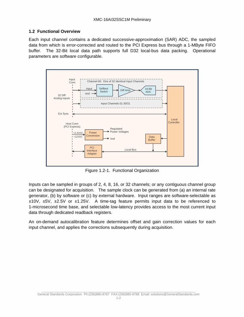
1.2 Functional Overview
Each input channel contains a dedicated successive-approximation (SAR) ADC, the sampled data from which is error-corrected and routed to the PCI Express bus through a 1-MByte FIFO buffer. The 32-Bit local data path supports full D32 local-bus data packing. Operational parameters are software configurable.
Figure 1.2-1. Functional Organization
Inputs can be sampled in groups of 2, 4, 8, 16, or 32 channels; or any contiguous channel group can be designated for acquisition. The sample clock can be generated from (a) an internal rate generator, (b) by software or (c) by external hardware. Input ranges are software-selectable as ±10V, ±5V, ±2.5V or ±1.25V. A time-tag feature permits input data to be referenced to 1-microsecond time base, and selectable low-latency provides access to the most current input data through dedicated readback registers.
An on-demand autocalibration feature determines offset and gain correction values for each input channel, and applies the corrections subsequently during acquisition.
PCIInterface Adapter
InputConn
32 DiffAnalog Inputs
DataBuffer
LocalController
Ext Sync
RegulatedPower Voltages
Vref
PowerConversion
Diff Amp 16-Bit ADC
Selftest Switch
Vref
Input
Channel-00: One of 32 Identical Input Channels
Input Channels 01-30/31
Local Bus
Host Conn(PCI Express)
+3.3VDC
+12VDC

XMC-16AI32SSC1M Preliminary
_____________________________________________________________________________ General Standards Corporation Ph:(256)880-8787 FAX:(256)880-8788 Email: [email protected]
2-1
SECTION 2.0
INSTALLATION AND MAINTENANCE 2.1 Board Configuration
This product has no field-alterable configuration features, and is completely configured at the factory for field use. 2.2 Installation
2.2.1 Physical Installation
To minimize the opportunity for accidental damage before installation, the board should be stored in the original protective shipping envelope. System power must be turned OFF before proceeding with the installation.
CAUTION: This product is susceptible to damage from electrostatic discharge (ESD). Before removing the board from the conductive shipping envelope, ensure that the work surface, the installer and the host board have been properly discharged to ground.
After removing the board from the shipping container, position the board with the P15 mezzanine connector facing the mating connector on the host board (Figure 2.2-1). Then carefully press the board into position on the host. Verify that the P15 connector has mated completely and that the board is seated firmly against the host. Then attach the board to the host by passing the mounting screws through the host board into the corresponding mounting holes in the standoffs and front-panel bezel. Tighten the screws carefully to complete the installation. Do not overtighten.
Figure 2.2-1. Mechanical Installation
2.2.2 Input/Output Cable Connections
System I/O connections are made through the 80-Pin front-panel system I/O connector (Figure 2.2-2), with the pin assignments listed in Table 2.2-1. The time tag function provides digital I/O pins for external synchronization.
P15 Connector
Standoff (2)
Standoff or XMC Bezel
2.5mm Mounting Screws (4)
Host PanelOpening

XMC-16AI32SSC1M Preliminary
_____________________________________________________________________________ General Standards Corporation Ph:(256)880-8787 FAX:(256)880-8788 Email: [email protected]
2-2
Auxiliary Sync I/O connections are made through a low-profile 6-Pin connector located on the back of the board (Side-2), with the pin assignments shown in Table 2.2-2. The auxiliary sync I/O connector is designed to mate with a Molex cable connector Model 51146-0600.
Table 2.2-1. System I/O Connector Pin Functions
ROW-A ROW-B
PIN SIGNAL PIN SIGNAL
1 INP00 LO 1 INP17 LO
2 INP00 HI 2 INP17 HI
3 INP01 LO 3 INP18 LO
4 INP01 HI 4 INP18 HI
5 INP02 LO 5 INP19 LO
6 INP02 HI 6 INP19 HI
7 INP03 LO 7 INP20 LO
8 INP03 HI 8 INP20 HI
9 INP04 LO 9 INP21 LO
10 INP04 HI 10 INP21 HI
11 INP05 LO 11 INPUT RTN
12 INP05 HI 12 INPUT RTN
13 INPUT RTN 13 INP22 LO
14 INPUT RTN 14 INP22 HI
15 INP06 LO 15 INP23 LO
16 INP06 HI 16 INP23 HI
17 INP07 LO 17 INP24 LO
18 INP07 HI 18 INP24 HI
19 INP08 LO 19 INP25 LO
20 INP08 HI 20 INP25 HI
21 INP09 LO 21 INP26 LO
22 INP09 HI 22 INP26 HI
23 INP10 LO 23 INPUT RTN
24 INP10 HI 24 INPUT RTN
25 INP11 LO 25 INP27 LO
26 INP11 HI 26 INP27 HI
27 INPUT RTN 27 INP28 LO
28 INPUT RTN 28 INP28 HI
29 INP12 LO 29 INP29 LO
30 INP12 HI 30 INP29 HI
31 INP13 LO 31 INP30 LO
32 INP13 HI 32 INP30 HI
33 INP14 LO 33 INP31 LO
34 INP14 HI 34 INP31 HI
35 INP15 LO 35 INPUT RTN
36 INP15 HI 36 REF CLK INP2
37 INP16 LO 37 DIG RTN
38 INP16 HI 38 CLOCK I/O1 or SAMP CLK INP
2
39 INPUT RTN 39 DIG RTN
40 CLOCK RST INP2 40 SYNC I/O
1 or SAMP CLK OUT
2
1 Default configuration. Not software-configured for time tagging. 2 If software-configured for time tagging.
System Mating Connector: Standard 80-pin 0.050" dual-ribbon socket connector: Robinson Nugent P50E-080S-TG or equivalent.

XMC-16AI32SSC1M Preliminary
_____________________________________________________________________________ General Standards Corporation Ph:(256)880-8787 FAX:(256)880-8788 Email: [email protected]
2-3
Figure 2.2-2. System I/O Connector
Table 2.2-2. Auxiliary Sync I/O Connections
SYNC-I/O CONN PIN 1 SIGNAL
1 DIG RTN
2 AUX CLOCK
3 DIG RTN
4 AUX SYNC
5 DIG RTN
6 Reserved. Connect to INPUT RTN or leave disconnected.
1 Recommended Sync-I/O mating cable connector is: Molex# 51146-0600.
Panel Pin-view
I/OCONN
PWB
ROW A ROW B
PIN 1
PIN 40
XMC-16AI32SSC1M Preliminary
_____________________________________________________________________________ General Standards Corporation Ph:(256)880-8787 FAX:(256)880-8788 Email: [email protected]
2-4
2.3 System Configuration
2.3.1 Analog Inputs
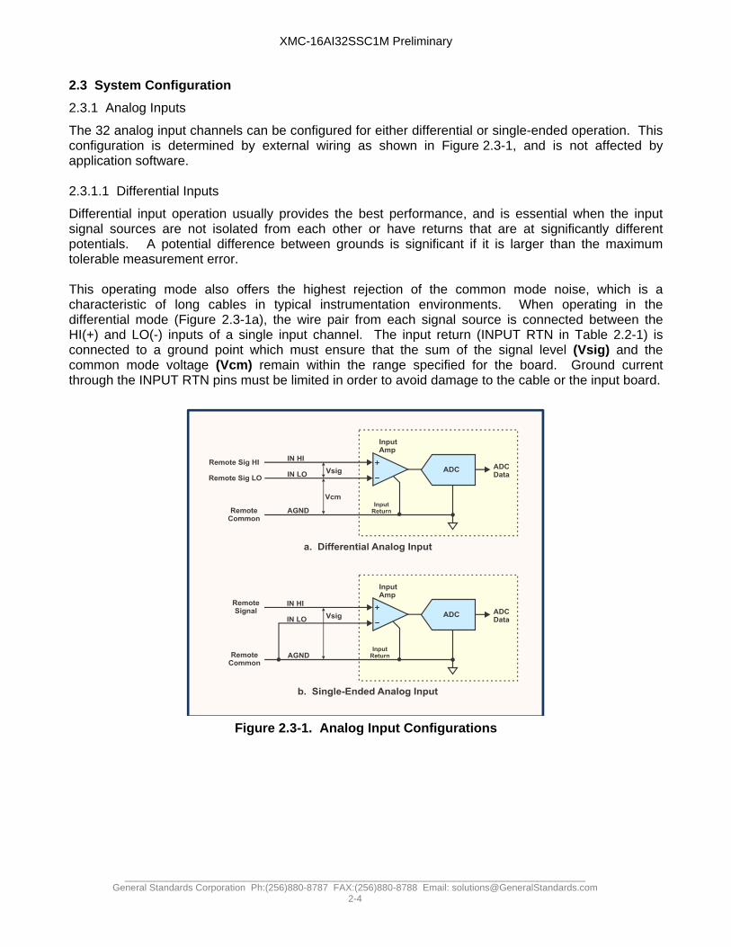
The 32 analog input channels can be configured for either differential or single-ended operation. This configuration is determined by external wiring as shown in Figure 2.3-1, and is not affected by application software. 2.3.1.1 Differential Inputs
Differential input operation usually provides the best performance, and is essential when the input signal sources are not isolated from each other or have returns that are at significantly different potentials. A potential difference between grounds is significant if it is larger than the maximum tolerable measurement error. This operating mode also offers the highest rejection of the common mode noise, which is a characteristic of long cables in typical instrumentation environments. When operating in the differential mode (Figure 2.3-1a), the wire pair from each signal source is connected between the HI(+) and LO(-) inputs of a single input channel. The input return (INPUT RTN in Table 2.2-1) is connected to a ground point which must ensure that the sum of the signal level (Vsig) and the common mode voltage (Vcm) remain within the range specified for the board. Ground current through the INPUT RTN pins must be limited in order to avoid damage to the cable or the input board.
Figure 2.3-1. Analog Input Configurations

XMC-16AI32SSC1M Preliminary
_____________________________________________________________________________ General Standards Corporation Ph:(256)880-8787 FAX:(256)880-8788 Email: [email protected]
2-5
2.3.1.2 Single-Ended Inputs
Single-ended operation (Figure 2.3-1b) generally provides acceptable performance only when the input signal sources either are isolated from each other, or are common to a single isolated signal return. A single-ended configuration usually is more susceptible to system interference than a differential configuration.
Single-ended inputs share a common input return that provides a return path for all inputs, making isolation from other system grounds a critical issue. If the signal sources are returned externally to system ground when operating in this mode, a potential difference between the system ground and input return can cause erroneous measurements, or could generate potentially destructive ground current.
For applications in which multiple signal sources share a single ground reference or return, the differential configuration is recommended, with all "LO" inputs connected together at the common remote return. 2.3.2 External Clock and Sync I/O
External clocking and synchronization behavior depends upon whether or not Time-Tagging (Appendix-C) is selected:
Time Tagging selected (Appendix C):
I/O pins A40, B36, B38 and B40 function as described in Paragraph c1.2.
Time Tagging not selected:
I/O Pins B38 and B40 function as described here for CLOCK I/O and SYNC I/O, respectively, and Pins A40 and B36 are nonfunctional inputs.
The CLOCK I/O and SYNC I/O pins in the I/O connector are bidirectional TTL signals that provide external control of analog input sampling and burst triggering. These signals are referenced to the DIG RTN pin, which is connected internally to PCI Express digital ground.
When configured as inputs by selection of the target mode, these pins accept clock and triggering signals from any external TTL source, including those originating on another XMC-16AI32SSC1M. For boards configured as initiators, the clock and sync pins become outputs that can be used to control external devices, including other XMC-16AI32SSC1M boards. Loading of initiator outputs should not exceed 10 milliamps. In the default state after power-up or initialization, both pins are configured as inputs. Clock and sync pins default to inputs (targets), and are pulled up internally to +3.3V through 33K-Ohms.
NOTE: The logic polarities of the clock and sync I/O pins can be inverted by application software.
2.3.2.1 External ADC Clocking
When the CLOCK I/O pin is configured as an input, all active input channels are sampled on the falling edge of a TTL input signal on this pin. Both the HIGH and LOW states of the clock input must have minimum durations of 100ns.

XMC-16AI32SSC1M Preliminary
_____________________________________________________________________________ General Standards Corporation Ph:(256)880-8787 FAX:(256)880-8788 Email: [email protected]
2-6
When configured as an initiator, the CLOCK I/O pin becomes a normally HIGH output that falls for 120-180ns at each occurrence of the internal ADC sample clock.
2.3.2.2 External Burst Triggering
When the SYNC I/O pin is configured as an input, a high-to-low TTL transition on this pin can be used to trigger an internal acquisition burst. Both HIGH and LOW sync input states must have durations of 100ns.
When configured as an initiator, the SYNC I/O pin becomes a normally HIGH output that falls for 120-180ns at the initiation of each internal triggered burst. 2.3.3 Auxiliary External Clock and Sync I/O
Two auxiliary external connections provide an alternate method of synchronizing sample clocking to external events. These TTL connections are available as AUX-CLOCK and AUX-SYNC (Table2.2-2), and are accessible through a low-profile 6-Pin connector on the edge of the board.
The AUX I/O pins can be programmed to be asserted either HIGH or LOW, and can be configured individually as inputs or outputs. Active AUX outputs produce an output pulse for each internal ADC sample clock or burst trigger. Source and sink load capacity of each output is 8 milliamps. Further details pertaining to these I/O functions are described in Section 3.9.
2.3.4 Multiboard Synchronization
If multiple boards are to be synchronized together, the CLOCK I/O and/or the SYNC I/O pins from one board, the initiator, are connected to the corresponding pins of one or more target boards (Figure 2.3-2). The controlling software determines specific clocking and burst triggering functions. The maximum number of targets depends upon both static loading and cable characteristics, and can vary typically from four to as many as eight.
Figure 2.3-2. Multiboard Synchronization
Note: Clock and Sync I/O pins can be designated independently as inputs(targets) or outputs (initiators).

XMC-16AI32SSC1M Preliminary
_____________________________________________________________________________ General Standards Corporation Ph:(256)880-8787 FAX:(256)880-8788 Email: [email protected]
2-7
2.4 Maintenance
This product requires no scheduled hardware maintenance other than periodic reference verification and possible adjustment. The optimum verification interval will vary, depending upon the specific application, but in most instances an interval of one year is sufficient.
In the event of a suspected malfunction, all associated system parameters, such as power voltages, control bus integrity, and system interface signal levels, should be evaluated before troubleshooting of the board itself is attempted. A board that has been determined to be defective should be returned to the factory for detailed problem analysis and repair.
2.5 Reference Verification
All analog input channels are software-calibrated to a single internal voltage reference by an embedded autocalibration firmware utility. The procedure presented here describes the verification and adjustment of the internal reference. 2.5.1 Equipment Required
Table 2.5-1 lists the equipment required for verifying or adjusting the internal reference. Alternative equivalent equipment may be used.
Table 2.5-1. Reference Verification Equipment
EQUIPMENT DESCRIPTION MANUFACTURER MODEL
Digital Multimeter, 5-1/2 digit, 0.005% accuracy for DC voltage measurements at ±10 Volts.
Hewlett Packard 34401A
Host board with single-width XMC site (Existing host) ---
Test cable; suitable for connecting the digital multimeter to two 0.02-inch square test posts.
--- ---
2.5.2 Verification and Adjustment
The following procedure describes the verification of the single reference voltage that ensures conformance to the product specification. Adjustment of the internal reference, if necessary, is performed with an internal trimmer that is accessible as shown in Figure 1.1-1.

XMC-16AI32SSC1M Preliminary
_____________________________________________________________________________ General Standards Corporation Ph:(256)880-8787 FAX:(256)880-8788 Email: [email protected]
2-8
This procedure assumes that the board to be adjusted is installed on an operational host:
1. Connect the digital multimeter between VCAL (+) Pin-3, and REF RTN (-) Pin-4 in the J4 test connector.
2. If power has been removed from the board, apply power now. Wait at least 10 minutes after power is applied before proceeding..
3. Select the ±10V input range.
4. Verify that the digital multimeter indication is +9.9900 VDC ±0.0008 VDC. If the indication is not within this range, adjust the INTERNAL REFERENCE trimmer accordingly.
5. Verification and adjustment is completed. Remove all test connections.

XMC-16AI32SSC1M Preliminary
_____________________________________________________________________________ General Standards Corporation Ph:(256)880-8787 FAX:(256)880-8788 Email: [email protected]
3-1
SECTION 3.0
CONTROL SOFTWARE 3.1 Introduction
The XMC-16AI32SSC1M is compatible with the IEEE PCI Express Specification revision 1.0a. A PLX PEX-8311 adapter operating in J-mode controls the interface. Configuration-space registers are initialized internally to support the location of the board on any 128 long-word boundary in memory space. After initialization has been completed, communication between the PCI Express bus and the local bus takes place through the control and data registers shown in Table 3.1-1. All local data transfers are long-word D32. Specific operational conditions identified throughout this section can invoke a single interrupt request from the board. DMA access is supported for data transfers from the analog input data buffer. The board identifies itself over the PCI Express bus with device, vendor and subsystem identification codes that are available from General Standards.
Table 3.1-1. Control and Data Registers
Offset (Hex)1
Register Access Mode 2 Default Primary Function Para Ref
0000 BOARD CONTROL (BCR) RW 0000 4070h Board Control Register (BCR) 3.2
0004 INTERRUPT CONTROL RW 0000 0008h Interrupt conditions and flags 3.7
0008 INPUT DATA BUFFER RO XXXX XXXXh Analog input data buffer 3.5.2
000C INPUT BUFFER CONTROL R/W 0003 FFFEh Input buffer threshold and control
0010 RATE-A GENERATOR RW 0001 0500h Rate-A generator freq selection 3.4.4
0014 RATE-B GENERATOR RW 0000 2000h Rate-B generator freq selection
0018 BUFFER SIZE RO 0000 0000h Number of values in the input buffer 3.5.2
001C BURST SIZE R/W 0000 0001h Number of sample clocks in a triggered burst.
3.12.1
0020 SCAN AND SYNC CONTROL R/W 0000 0005h Channels per scan; Clock and Sync sources.
3.4.2
0024 ACTIVE CHANNEL ASSIGNMENT R/W 0000 0100h Specific first and last active channels. 3.4.2.2
0028 BOARD CONFIGURATION RO 00XX XXXXh Firmware revision and option straps. 3.10
002C Autocal Values 3 R/W 0000 080Xh Autocal value readback. ---
0030 Auxiliary R/W Register 3 R/W 0000 0000h Auxiliary register. For internal use only. ---
0034 AUXILIARY SYNC I/O CONTROL R/W 0000 0000h Controls the auxiliary sync I/O port 3.9
0038 SCAN MARKER UPPER WORD R/W 0000 0000h Packed-data scan marker D[31..16]. 3.11
003C SCAN MARKER LOWER WORD R/W 0000 0000h Packed-data scan marker D[15..0].
0040 Low Latency Control R/W 0000 07C0h Low Latency hold and release channels 3.14
0044-004C (Reserved) RO 0000 0000h --- ---
0050-00FC Time Tag register field --- --- --- App-C
0100-17C Low-Latency Data RO 0000 XXXXh Low Latency data 3.14
0180-1FC (Reserved) RO --- --- ---
1 Offsets from the PCI base address for local addressing. 2 R/W = Read/Write; RO = Read-Only. 3 Maintenance register. Shown for reference only.
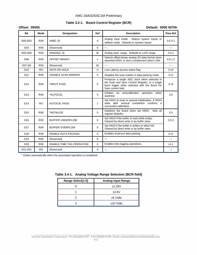
3.2 Board Control Register (BCR)
The Board Control Register (BCR) controls primary board functions, including the analog input mode and voltage range. Table 3.2-1 provides a brief description of each bit field in the BCR, as well as indicating an associated section in the text.

XMC-16AI32SSC1M Preliminary
_____________________________________________________________________________ General Standards Corporation Ph:(256)880-8787 FAX:(256)880-8788 Email: [email protected]
3-2
Table 3.2-1. Board Control Register (BCR) Offset: 0000h Default: 0000 4070h
Bit Mode Designation Def Description Para Ref
D00-D02 R/W AIM[2..0] 0 Analog input mode. Selects system inputs or selftest mode. Defaults to System Inputs
3.5.3.1
D03 R/W (Reserved) 0 --- ---
D04-D05 R/W RANGE[1..0] 3h Analog input range. Defaults to ±10V range. 3.4.1
D06 R/W OFFSET BINARY 1 Selects offset-binary analog I/O data format when asserted HIGH, or two's complement when LOW. 3.5.1.2
D07-D9 R/W (Reserved) 0h --- ---
D10 RO DATA ON HOLD 0 Low-Latency access status flag. 3.14
D11 R/W DISABLE SCAN MARKER 0 Disables the scan marker in data packing mode. 3.11
D12 R/W *INPUT SYNC 0
Produces a single ADC clock when selected in the Scan and Sync Control Register, or a single burst trigger when selected with the Burst On Sync control field.
3.12
D13 R/W *AUTOCAL 0 Initiates an autocalibration operation when asserted. 3.6
D14 RO AUTOCAL PASS 1 Set HIGH at reset or autocal initialization. A HIGH state after autocal completion confirms a successful calibration.
D15 R/W *INITIALIZE 0 Initializes the board when set HIGH. Sets all register defaults. 3.3
D16 R/W BUFFER UNDERFLOW 0 Set HIGH if the buffer is read while empty. Cleared by direct write or by buffer clear. 3.5.2
D17 R/W BUFFER OVERFLOW 0 Set HIGH if the buffer is written to when full. Cleared by direct write or by buffer clear.
D18 R/W ENABLE DATA PACKING 0 Enables local-bus data packing 3.11
D19 R/W (Reserved) 0 --- ---
D20 R/W ENABLE TIME TAG OPERATION 0 Enables time tagging operations. c1.1
D21-D31 RO (Reserved) 0 --- ---
* Clears automatically when the associated operation is completed.
3.3 Initialization
3.3.1 Configuration
During board configuration, initial values for both the PCI Express configuration registers and the internal control logic are extracted from internal nonvolatile read-only memory. This process is initiated by a bus reset, and should be required only once after the initial application of power. While the configuration registers are being loaded, the response to target accesses is RETRY's. Configuration operations are executed in the sequence shown in Table 3.3-1. Board configuration terminates with the PCI Express interrupt disabled.
Table 3.3-1. Configuration Operations
Operation Maximum Duration PCI Express configuration registers are loaded from internal ROM 3 ms Internal control logic is configured from internal ROM 300 ms Internal control logic is initialized 3 ms

XMC-16AI32SSC1M Preliminary
_____________________________________________________________________________ General Standards Corporation Ph:(256)880-8787 FAX:(256)880-8788 Email: [email protected]
3-3
3.3.2 Local Controller Initialization
Internal control logic can be initialized without reconfiguration of the PCI Express registers by setting the INITIALIZE control bit in the BCR. This action initializes the internal logic, but does not affect the PCI Express configuration registers and does not reconfigure the internal control logic. Initialization requires 3 milliseconds or less for completion, and produces the following default conditions:
The BCR is initialized; all defaults are invoked (Table 3.2-1),
Analog input voltage range is ±10 Volts (Tables 3.2-1, 3.4-1),
All available channels are active (Table 3.4-2),
Input sample clocking is disabled (Tables 3.4-2, 3.4-4),
Rate-A generator is adjusted for a 50 kHz sample rate, and is disabled (Tables 3.4-4, 3.4-5).
Analog input data coding format is offset binary; Data packing is disabled (Table 3.5-2),
The analog input buffer is reset to empty (Tables 3.5-3. 3.5-4),
Upon completion of initialization, the INITIALIZE control bit is cleared automatically. 3.4 Analog Input Parameters
3.4.1 Input Voltage Range
BCR control field RANGE[] (Table 3.4-1) selects the analog input voltage range.
Table 3.4-1. Analog Voltage Range Selection
Range Select[1:0] Analog Input Range
0 ±1.25V
1 ±2.5V
2 ±5 Volts
3 ±10 Volts
3.4.2 Active Channel Selection
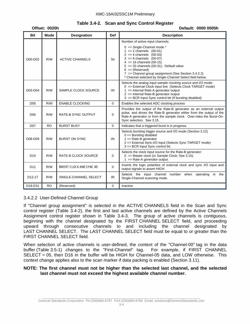
NOTE: The Scan and Sync control register (Table 3.4-2) controls the selection of active channels, as well as the configuration of internal timing signals.
3.4.2.1 Predetermined Channel Group
The analog inputs can be sampled in groups of 2, 4, 8, 16 or 32 active channels, or any single channel can be selected for digitizing. The number of active channels is selected by the ACTIVE CHANNELS[] field in the scan and sync control register. Each active channel group commences with Channel-00, and proceeds upward through successive channels to the selected number of channels.
For Single-Channel sampling (ACTIVE CHANNELS[] = 0), the channel to be digitized is selected by the SINGLE-CHANNEL SELECT control field.
XMC-16AI32SSC1M Preliminary
_____________________________________________________________________________ General Standards Corporation Ph:(256)880-8787 FAX:(256)880-8788 Email: [email protected]
3-4
Table 3.4-2. Scan and Sync Control Register Offset: 0020h Default: 0000 0005h
Bit Mode Designation Def Description
D00-D02 R/W ACTIVE CHANNELS 5h
Number of active input channels:
0 => Single-Channel mode * 1 => 2 channels (00-01) 2 => 4 channels (00-03) 3 => 8 channels (00-07) 4 => 16 channels (00-15) 5 => 32 channels (00-31); Default value 6 => (Reserved) 7 => Channel group assignment (See Section 3.4.2.2) * Channel selected by Single-Channel Select field below.
D03-D04 R/W SAMPLE CLOCK SOURCE 0h
Selects the analog input sample clocking source and I/O mode: 0 => External Clock input line (Selects Clock TARGET mode) 1 => Internal Rate-A generator output 2 => Internal Rate-B generator output 3 => BCR Input Sync control bit (If bursting disabled)
D05 R/W ENABLE CLOCKING 0 Enables the selected ADC clocking process
D06 R/W RATE-B SYNC OUTPUT 0
Provides the output of the Rate-B generator as an external output pulse, and drives the Rate-B generator either from the output of the Rate-A generator or from the sample clock. Over-rides the Burst-On-Sync selection. See 3.15.
D07 RO BURST BUSY 0 Indicates that a triggered burst is in progress.
D08-D09 R/W BURST ON SYNC 0h
Selects bursting trigger source and I/O mode (Section 3.12) 0 => Bursting disabled 1 => Rate-B generator 2 => External Sync-I/O input (Selects Sync TARGET mode) 3 => BCR Input Sync control bit.
D10 R/W RATE-B CLOCK SOURCE 0 Selects the clock input source for the Rate-B generator: 0 => Master clock (or Sample Clock; See 3.15). 1 => Rate-A generator output.
D11 R/W INVERT CLOCK AND SYNC I/O 0 Inverts the logic polarities of external clock and sync I/O input and output signals to assert HIGH.
D12-17 R/W SINGLE-CHANNEL SELECT 0h Selects the input channel number when operating in the Single-Channel scanning mode.
D18-D31 RO (Reserved) 0 Inactive
3.4.2.2 User-Defined Channel Group
If "Channel group assignment" is selected in the ACTIVE CHANNELS field in the Scan and Sync control register (Table 3.4-2), the first and last active channels are defined by the Active Channels Assignment control register shown in Table 3.4-3. The group of active channels is contiguous, beginning with the channel designated by the FIRST CHANNEL SELECT field, and proceeding upward through consecutive channels to and including the channel designated by LAST CHANNEL SELECT. The LAST CHANNEL SELECT field must be equal to or greater than the FIRST CHANNEL SELECT field.
When selection of active channels is user-defined, the context of the "Channel-00" tag in the data buffer (Table 3.5-1) changes to the "First-Channel" tag. For example, if FIRST CHANNEL SELECT = 05, then D16 in the buffer will be HIGH for Channel-05 data, and LOW otherwise. This context change applies also to the scan marker if data packing is enabled (Section 3.11).
NOTE: The first channel must not be higher than the selected last channel, and the selected last channel must not exceed the highest available channel number.

XMC-16AI32SSC1M Preliminary
_____________________________________________________________________________ General Standards Corporation Ph:(256)880-8787 FAX:(256)880-8788 Email: [email protected]
3-5
Table 3.4-3. User-Defined Active Channel Assignment Offset: 0000 0024h Default: 0000 0100h
Data Bit Mode Designation Default Description
D00-D07 R/W FIRST CHANNEL SELECT 0 First (lowest-numbered) active channel
D08-D15 R/W LAST CHANNEL SELECT 1 Last (highest-numbered) active channel
D16-D31 RO (Reserved) 0 Inactive. Returns all-zero.
3.4.3 Timing Organization
Figure 3.4-1 illustrates the manner in which ADC timing signals are organized within the board. The input sample clock selector is controlled by the Scan and Sync control register, which provides direct software control of clocking and sync operations. The bidirectional external clock I/O pin provides external control of ADC clocking.
Figure 3.4-1. Sample Clock Organization
Two internal rate generators operate directly from the master clock frequency, or can be cascaded. A sample clock can be generated by (a) an internal rate generator, (b) the INPUT SYNC control bit in the BCR, or (c) an external clock source. Each sample clock produces a sample of all active input channels.
NOTE: The logic polarities of the external clock and sync I/O pins can be inverted by setting
the INVERT CLOCK AND SYNC I/O control bit HIGH in the Scan and Sync control register (Paragraph 2.3.2 and Table 3.4-2). This inversion does not affect the Auxiliary Clock and Sync logic polarities selected in Table 3.9-1.
3.4.4 Sample Rate Control
All active channels are sampled, or clocked, simultaneously from the source selected by the SAMPLE CLOCK SOURCE control field in the Scan and Sync control register. NOTE: ADC sampling (clocking), is disabled while the ENABLE CLOCKING control bit is LOW,
or is enabled when this bit is set HIGH.
Sample ClockGen A
Nrate-A
Gen B
Ext Clock Input/Output
Master ClockFgen-A
Fgen-B
Nrate-B(Initiator)
(Target)
BCR Sync

XMC-16AI32SSC1M Preliminary
_____________________________________________________________________________ General Standards Corporation Ph:(256)880-8787 FAX:(256)880-8788 Email: [email protected]
3-6
NOTE: If bursting is disabled, a single sample of all inputs can be obtained by asserting the
INPUT_SYNC control bit HIGH in the BCR. This bit clears automatically.
3.4.4.1 Sample Rate Generators
Each of two rate generators consists of a 16-bit down-counter that divides the master clock frequency by a 16-bit integer contained in the associated rate control register. The two rate control registers are organized as shown in Table 3.4-4. Bits D00-D15 represent the frequency divisor Nrate, and D16 disables the associated generator when set HIGH. D16 defaults to the HIGH (disable) state in the Rate-A control register.
Table 3.4-4. Rate Generator Control Register
Offset: 0010h (Rate-A), 0014h (Rate-B) Default: 0001 0500h (Rate-A), 0000 2000h (Rate-B)
Data Bit Mode Designation Default Description
D00-D15 R/W NRATE --- Rate generator frequency control
D16 R/W GENERATOR DISABLE 1 Disables the rate generator when HIGH
D17-D31 RO (Inactive) 0 ---
3.4.4.2 Rate Generator Frequency Control
Each rate generator is controlled by a divisor Nrate that can be adjusted up to a maximum value of FFFFh (65535 decimal). With a master clock frequency of Fclk, the output frequency Fgen of each generator is determined as:
Fgen (Hz) = Fclk (Hz) / Nrate,
where Nrate is the decimal equivalent of D00-D15 in the rate generator control register. Fgen is the sampling frequency, and equals the rate at which all active channels are sampled. Fclk has a standard value of 64 MHz, but may have other values depending upon custom ordering options.
The maximum sampling frequency Fgen-max is 1.0 MHz.
Table 3.4-5. Rate Generator Frequency Selection
Nrate ( RATE[15..0] ) Fgen
with 64 MHz Master Clock
(Dec) (Hex) (Hz, or Samples per second: SPS )
64 40 1,000,000
1280 500 50,000
--- --- Fgen (Hz) = 64,000,000 / Nrate

XMC-16AI32SSC1M Preliminary
_____________________________________________________________________________ General Standards Corporation Ph:(256)880-8787 FAX:(256)880-8788 Email: [email protected]
3-7
3.4.4.3 Generator Cascading
To obtain very low sampling or burst-triggering rates, the Rate-B generator can be configured with the RATE-B CLOCK SOURCE control field to operate from the output of the Rate-A generator instead of from the master clock. When operating in this cascaded configuration, the output frequency of the Rate-B generator is:
Fgen-B (Hz) = Fclk / (Nrate-A * Nrate-B ) ,
which can produce sample rates as low as 0.015 Hz with Fclk = 64 MHz. 3.4.5 External Clock and Sync I/O
Multiple boards can be interconnected externally to produce synchronous analog input sampling and burst triggering. Figure 2.3-2 illustrates the interconnections required. One of the boards is designated as the Initiator, and the remaining boards are designated as targets.
A board that is enabled for external sync I/O is designated as a clock target by selecting 'External Clock Input Line' in the SAMPLE CLOCK SOURCE control field of the Scan and Sync control register. An external clock input signal can originate either from an initiator board, or from an independent TTL source. Any other value for this field designates the board as a clock initiator.
A clock initiator generates an output clock pulse in conjunction with each internal ADC sample clock, and each of the target boards responds to the clock pulse by acquiring a single sample of all of its designated active channels.
External burst triggering I/O is implemented in the same manner as external clocking I/O, but the trigger source is selected through the BURST ON SYNC control field in the Scan and Sync control register, and the SYNC I/O pin provides the external trigger interface connection.
NOTES: To avoid contention on the SYNC I/O and CLOCK I/O lines, no more than one
board can be designated as sync or clock initiator.
For optimum autocalibration effectiveness at rates above 50 KSPS, adjust the Rate-A Generator register to the same value on all boards.
Refer to Paragraphs 3.9 and 3.15 for alternative external clock and sync provisions.
3.5 Analog Data Control
3.5.1 Input Data Organization
Processed conversion data from the analog-to-digital converters (ADC's) flows into the analog input FIFO data buffer, and from the data buffer to the PCI Express bus as analog input data. The data buffer appears to the bus as a single read-only register. 3.5.1.1 Input Data Buffer
Nonpacked analog input data is right-justified to the LSB, and occupies bit positions D00 through D15 (Table 3.5-1). D31 is the Channel-00 tag, which is asserted when the data field contains Channel-00 data. The Channel-00 tag is not available for packed data, nor when operating in the optional time-tagging mode (Appendix-C)

XMC-16AI32SSC1M Preliminary
_____________________________________________________________________________ General Standards Corporation Ph:(256)880-8787 FAX:(256)880-8788 Email: [email protected]
3-8
The intermediate bit field is all-zero unless two's complement coding is selected, in which case the reserved bits become the sign extension. When selection of active channels is user-defined (3.4.2.2), the context of the "Channel-00 tag" in the data buffer becomes the "First-Channel tag."
An empty buffer returns an indeterminate value. Refer to Paragraph 3-11 for the configuration of packed data, and for the effect of data packing on buffer contents.
Table 3.5-1. Input Data Buffer; Nonpacked Data Offset: 0008h Default: N/A
Channel-00 Tag Reserved * (Zero) Channel Data Value
Data Bit(s) D[31] D[30..16] D[15..0]
All fields are read-only; Write-data is ignored.
3.5.1.2 Data Coding Format
Analog input data is arranged in a right-justified data field with the coding conventions shown in Table 3.5-2. The default format is offset binary. Two's complement format is selected by clearing the OFFSET BINARY control bit LOW in the BCR. Unless indicated otherwise, offset binary coding is assumed throughout this document.
Table 3.5-2. Input Data Coding
16-Bit Digital Value (Hex)
Analog Input Level Offset Binary Two's Complement
Positive Full Scale minus 1 LSB FFFF 7FFF
Zero (Midscale) 8000 0000
Zero minus 1 LSB 7FFF FFFF
Negative Full Scale 0000 8000
XMC-16AI32SSC1M Preliminary
_____________________________________________________________________________ General Standards Corporation Ph:(256)880-8787 FAX:(256)880-8788 Email: [email protected]
3-9
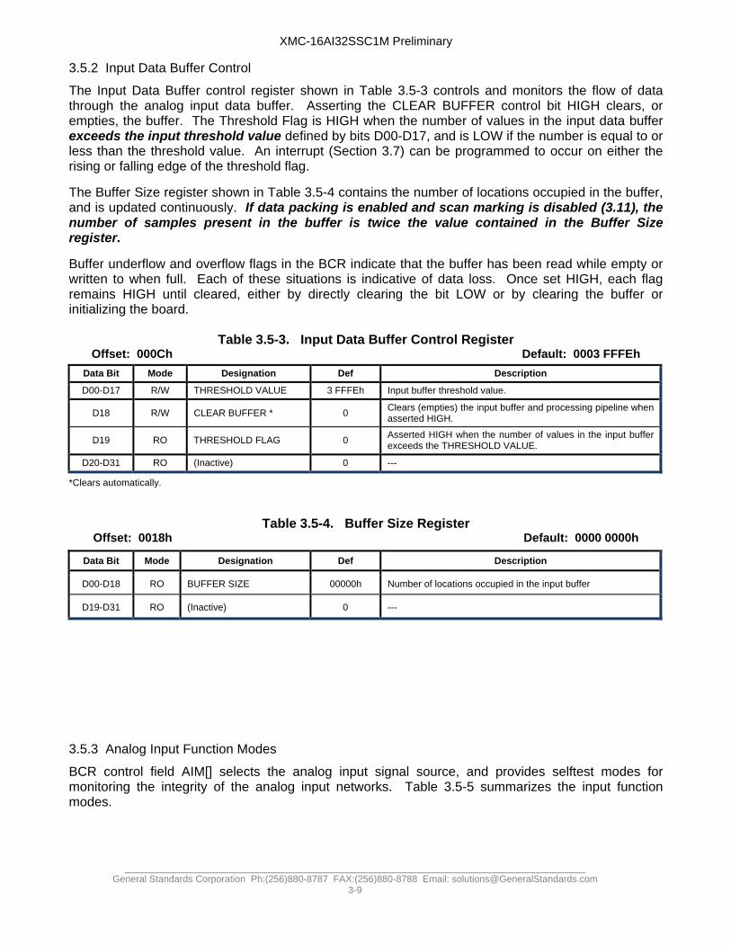
3.5.2 Input Data Buffer Control
The Input Data Buffer control register shown in Table 3.5-3 controls and monitors the flow of data through the analog input data buffer. Asserting the CLEAR BUFFER control bit HIGH clears, or empties, the buffer. The Threshold Flag is HIGH when the number of values in the input data buffer exceeds the input threshold value defined by bits D00-D17, and is LOW if the number is equal to or less than the threshold value. An interrupt (Section 3.7) can be programmed to occur on either the rising or falling edge of the threshold flag.
The Buffer Size register shown in Table 3.5-4 contains the number of locations occupied in the buffer, and is updated continuously. If data packing is enabled and scan marking is disabled (3.11), the number of samples present in the buffer is twice the value contained in the Buffer Size register.
Buffer underflow and overflow flags in the BCR indicate that the buffer has been read while empty or written to when full. Each of these situations is indicative of data loss. Once set HIGH, each flag remains HIGH until cleared, either by directly clearing the bit LOW or by clearing the buffer or initializing the board.
Table 3.5-3. Input Data Buffer Control Register Offset: 000Ch Default: 0003 FFFEh
Data Bit Mode Designation Def Description
D00-D17 R/W THRESHOLD VALUE 3 FFFEh Input buffer threshold value.
D18 R/W CLEAR BUFFER * 0 Clears (empties) the input buffer and processing pipeline when asserted HIGH.
D19 RO THRESHOLD FLAG 0 Asserted HIGH when the number of values in the input buffer exceeds the THRESHOLD VALUE.
D20-D31 RO (Inactive) 0 ---
*Clears automatically.
Table 3.5-4. Buffer Size Register Offset: 0018h Default: 0000 0000h
Data Bit Mode Designation Def Description
D00-D18 RO BUFFER SIZE 00000h Number of locations occupied in the input buffer
D19-D31 RO (Inactive) 0 ---
3.5.3 Analog Input Function Modes
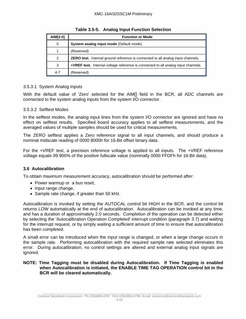
BCR control field AIM[] selects the analog input signal source, and provides selftest modes for monitoring the integrity of the analog input networks. Table 3.5-5 summarizes the input function modes.
XMC-16AI32SSC1M Preliminary
_____________________________________________________________________________ General Standards Corporation Ph:(256)880-8787 FAX:(256)880-8788 Email: [email protected]
3-10
Table 3.5-5. Analog Input Function Selection
AIM[2:0] Function or Mode
0 System analog input mode (Default mode).
1 (Reserved)
2 ZERO test. Internal ground reference is connected to all analog input channels.
3 +VREF test. Internal voltage reference is connected to all analog input channels.
4-7 (Reserved)
3.5.3.1 System Analog Inputs
With the default value of 'Zero' selected for the AIM[] field in the BCR, all ADC channels are connected to the system analog inputs from the system I/O connector. 3.5.3.2 Selftest Modes
In the selftest modes, the analog input lines from the system I/O connector are ignored and have no effect on selftest results. Specified board accuracy applies to all selftest measurements, and the averaged values of multiple samples should be used for critical measurements.
The ZERO selftest applies a Zero reference signal to all input channels, and should produce a nominal midscale reading of 0000 8000h for 16-Bit offset binary data. For the +VREF test, a precision reference voltage is applied to all inputs. The +VREF reference voltage equals 99.900% of the positive fullscale value (nominally 0000 FFDFh for 16-Bit data).
3.6 Autocalibration
To obtain maximum measurement accuracy, autocalibration should be performed after:
Power warmup or a bus reset, Input range change, Sample rate change, if greater than 50 kHz.
Autocalibration is invoked by setting the AUTOCAL control bit HIGH in the BCR, and the control bit returns LOW automatically at the end of autocalibration. Autocalibration can be invoked at any time, and has a duration of approximately 2.0 seconds. Completion of the operation can be detected either by selecting the 'Autocalibration Operation Completed' interrupt condition (paragraph 3.7) and waiting for the interrupt request, or by simply waiting a sufficient amount of time to ensure that autocalibration has been completed.
A small error can be introduced when the input range is changed, or when a large change occurs in the sample rate. Performing autocalibration with the required sample rate selected eliminates this error. During autocalibration, no control settings are altered and external analog input signals are ignored. NOTE: Time Tagging must be disabled during Autocalibration. If Time Tagging is enabled
when Autocalibration is initiated, the ENABLE TIME TAG OPERATION control bit in the BCR will be cleared automatically.
XMC-16AI32SSC1M Preliminary
_____________________________________________________________________________ General Standards Corporation Ph:(256)880-8787 FAX:(256)880-8788 Email: [email protected]
3-11
To compensate for component aging, and to minimize the effects of temperature on accuracy, the autocalibration function determines the optimum calibration values for current conditions, and stores the necessary correction values in volatile memory. If a board is defective, the autocalibration process may be unable to successfully calibrate the inputs. If this situation occurs, the AUTOCAL PASS status bit in the BCR is cleared LOW at the end of the autocalibration interval, and remains LOW until a subsequent initialization or autocalibration occurs. AUTOCAL PASS is initialized HIGH, and remains HIGH unless an autocalibration failure occurs.
NOTE: The autocalibration utility uses the contents of the Rate-A generator control register to establish the ADC sample rate used during test-signal acquisition. For optimal calibration effectiveness when clocking the inputs from a source other than the Rate-A generator, adjust the Rate-A generator control register to approximately the value that would produce the expected sample rate (Section 3.4.4).
3.7 Interrupt Control
In order for the board to generate a PCI Express interrupt, both of the following conditions must occur:
a. The internal controller must generate a Local Interrupt Request b. PCI Express interrupt emulation must be enabled.
If the internal controller generates a local interrupt request, a PCI Express interrupt will not occur unless the PCI Express interrupt has been enabled. 3.7.1 Local Interrupt Request
The Interrupt Control Register shown in Table 3.7-1 controls the single local interrupt request line. Two simultaneous source conditions (IRQ 0 and1) are available for the request, with multiple conditions available for each source. IRQ 0 and 1 are logically OR'd together to produce the single interrupt available to the board.
When one or more selected conditions occur for either of the IRQ's, a local interrupt request is generated and the associated IRQ REQUEST flag bit is set HIGH. The request remains asserted until the PCI bus clears the request flag. A local interrupt request is generated automatically at the end of initialization, through IRQ0.
Interrupt conditions are edge-sensitive, and an interrupt request is generated if a selected interrupt condition undergoes a transition from 'false' (not-true) to 'true' while that condition is selected. 3.7.2 Enabling the PCI Express Interrupt
A local interrupt request will not produce an interrupt on the PCI Express bus unless interrupt emulation is enabled. Refer to the PEX-8311 reference manual for details pertaining to this function
XMC-16AI32SSC1M Preliminary
_____________________________________________________________________________ General Standards Corporation Ph:(256)880-8787 FAX:(256)880-8788 Email: [email protected]
3-12
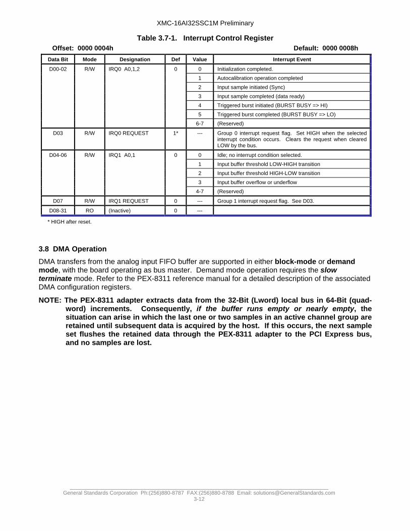
Table 3.7-1. Interrupt Control Register Offset: 0000 0004h Default: 0000 0008h
Data Bit Mode Designation Def Value Interrupt Event
D00-02 R/W IRQ0 A0,1,2 0 0 Initialization completed.
1 Autocalibration operation completed
2 Input sample initiated (Sync)
3 Input sample completed (data ready)
4 Triggered burst initiated (BURST BUSY => HI)
5 Triggered burst completed (BURST BUSY => LO)
6-7 (Reserved)
D03 R/W IRQ0 REQUEST 1* --- Group 0 interrupt request flag. Set HIGH when the selected interrupt condition occurs. Clears the request when cleared LOW by the bus.
D04-06 R/W IRQ1 A0,1 0 0 Idle; no interrupt condition selected.
1 Input buffer threshold LOW-HIGH transition
2 Input buffer threshold HIGH-LOW transition
3 Input buffer overflow or underflow
4-7 (Reserved)
D07 R/W IRQ1 REQUEST 0 --- Group 1 interrupt request flag. See D03.
D08-31 RO (Inactive) 0 ---
* HIGH after reset.
3.8 DMA Operation
DMA transfers from the analog input FIFO buffer are supported in either block-mode or demand mode, with the board operating as bus master. Demand mode operation requires the slow terminate mode. Refer to the PEX-8311 reference manual for a detailed description of the associated DMA configuration registers.
NOTE: The PEX-8311 adapter extracts data from the 32-Bit (Lword) local bus in 64-Bit (quad-word) increments. Consequently, if the buffer runs empty or nearly empty, the situation can arise in which the last one or two samples in an active channel group are retained until subsequent data is acquired by the host. If this occurs, the next sample set flushes the retained data through the PEX-8311 adapter to the PCI Express bus, and no samples are lost.

XMC-16AI32SSC1M Preliminary
_____________________________________________________________________________ General Standards Corporation Ph:(256)880-8787 FAX:(256)880-8788 Email: [email protected]
3-13
3.9 Auxiliary External Clock and Sync I/O
Two auxiliary external connections provide an alternate method of synchronizing sample clocking and burst triggering to external events. These bidirectional TTL connections are available as AUX CLOCK and AUX SYNC (Table 2.2-2), and when active as inputs, replace the corresponding external CLOCK I/O and SYNC I/O inputs in the system I/O connector. The AUX I/O signals are accessible through a 6-Pin connector on the back (Side-2) of the board.
AUX clock and sync signals are designated independently through the Auxiliary Sync I/O Control register as inputs, outputs, or inactive, as indicated in Table 3.9-1. When an AUX signal is designated as an input, the signal replaces the corresponding CLOCK I/O or SYNC IO input from the system connector. In order for the input to be acknowledged, target mode must be selected in the corresponding clock or sync control field in the Scan and Sync control register (Table 3.4-2). The AUX I/O pins are pulled up internally to +3.3VDC through 4.7K.
Active AUX outputs produce an output pulse for each internal ADC sample clock or burst trigger, and are active in both target and initiator clock and sync modes.
To increase the reliability of external triggering in high-noise environments, selectable noise suppression increases the debounce or detection interval for active inputs, and increases the pulse width of active outputs.
AUX inputs are edge-detected as LOW-to-HIGH transitions if the INVERT INPUTS control bit is LOW, or as HIGH-to-LOW transitions if the bit is HIGH. Minimum HIGH and LOW level durations are 100ns if the NOISE SUPPRESSION control bit is LOW, or 1.5us if the bit is HIGH. AUX output pulses are positive (i.e.: baseline level is LOW) if the INVERT OUTPUTS control bit is LOW, or negative (baseline HIGH) if the control bit is HIGH. Output pulse width is typically 130ns if the NOISE SUPPRESSION control bit is LOW, or 2.0us if the bit is HIGH.
XMC-16AI32SSC1M Preliminary
_____________________________________________________________________________ General Standards Corporation Ph:(256)880-8787 FAX:(256)880-8788 Email: [email protected]
3-14
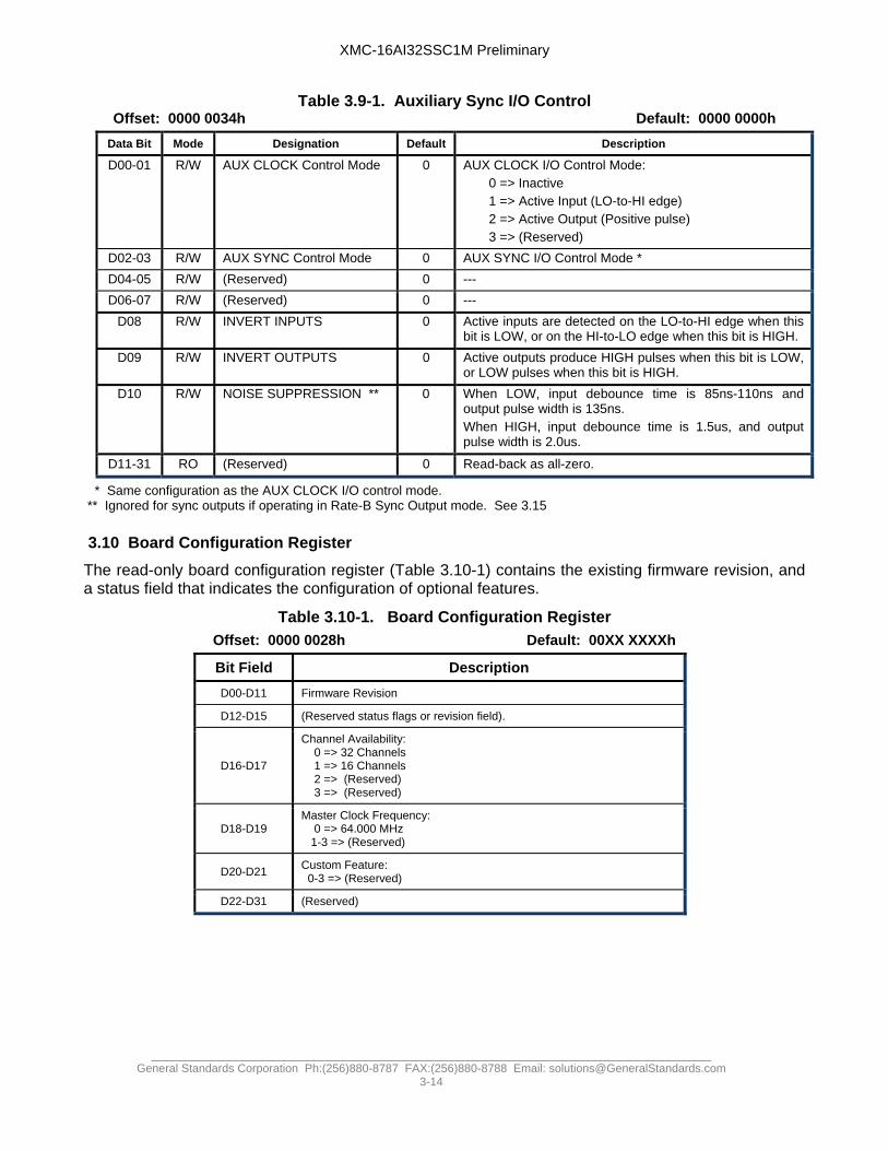
Table 3.9-1. Auxiliary Sync I/O Control
Offset: 0000 0034h Default: 0000 0000h
Data Bit Mode Designation Default Description
D00-01 R/W AUX CLOCK Control Mode 0 AUX CLOCK I/O Control Mode: 0 => Inactive 1 => Active Input (LO-to-HI edge) 2 => Active Output (Positive pulse) 3 => (Reserved)
D02-03 R/W AUX SYNC Control Mode 0 AUX SYNC I/O Control Mode *
D04-05 R/W (Reserved) 0 ---
D06-07 R/W (Reserved) 0 ---
D08 R/W INVERT INPUTS 0 Active inputs are detected on the LO-to-HI edge when this bit is LOW, or on the HI-to-LO edge when this bit is HIGH.
D09 R/W INVERT OUTPUTS 0 Active outputs produce HIGH pulses when this bit is LOW, or LOW pulses when this bit is HIGH.
D10 R/W NOISE SUPPRESSION ** 0 When LOW, input debounce time is 85ns-110ns and output pulse width is 135ns. When HIGH, input debounce time is 1.5us, and output pulse width is 2.0us.
D11-31 RO (Reserved) 0 Read-back as all-zero.
* Same configuration as the AUX CLOCK I/O control mode. ** Ignored for sync outputs if operating in Rate-B Sync Output mode. See 3.15
3.10 Board Configuration Register
The read-only board configuration register (Table 3.10-1) contains the existing firmware revision, and a status field that indicates the configuration of optional features.
Table 3.10-1. Board Configuration Register
Offset: 0000 0028h Default: 00XX XXXXh
Bit Field Description
D00-D11 Firmware Revision
D12-D15 (Reserved status flags or revision field).
D16-D17
Channel Availability: 0 => 32 Channels 1 => 16 Channels 2 => (Reserved) 3 => (Reserved)
D18-D19 Master Clock Frequency: 0 => 64.000 MHz 1-3 => (Reserved)
D20-D21 Custom Feature: 0-3 => (Reserved)
D22-D31 (Reserved)
XMC-16AI32SSC1M Preliminary
_____________________________________________________________________________ General Standards Corporation Ph:(256)880-8787 FAX:(256)880-8788 Email: [email protected]
3-15
3.11 Data Packing
Data packing enables the entire 32-Bit local bus to be used to convey data to the PCI Express bus. Setting the ENABLE DATA PACKING control bit high in the BCR selects the data packing mode, in which two consecutive 16-bit data values are packed into a single 32-Bit local data longword. In the data packing mode, a 32-bit scan marker code is inserted directly before each Channel-00 data value in the buffer (or immediately before the 'first channel' if the active channels are user-defined (3.4.2.2). The scan marker can be disabled by setting the DISABLE SCAN MARKER control bit HIGH in the BCR.
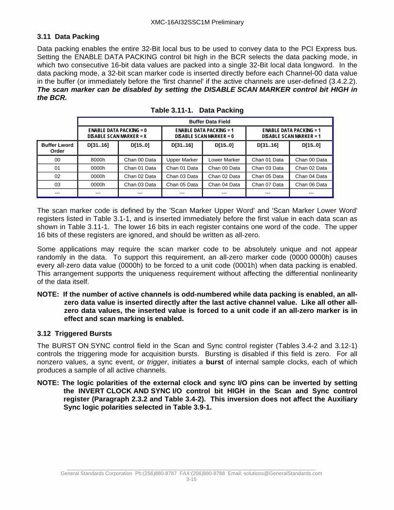
Table 3.11-1. Data Packing
Buffer Data Field
ENABLE DATA PACKING = 0 DISABLE SCAN MARKER = X
ENABLE DATA PACKING = 1 DISABLE SCAN MARKER = 0
ENABLE DATA PACKING = 1 DISABLE SCAN MARKER = 1
Buffer Lword Order
D[31..16] D[15..0] D[31..16] D[15..0] D[31..16] D[15..0]
00 8000h Chan 00 Data Upper Marker Lower Marker Chan 01 Data Chan 00 Data
01 0000h Chan 01 Data Chan 01 Data Chan 00 Data Chan 03 Data Chan 02 Data
02 0000h Chan 02 Data Chan 03 Data Chan 02 Data Chan 05 Data Chan 04 Data
03 0000h Chan 03 Data Chan 05 Data Chan 04 Data Chan 07 Data Chan 06 Data
--- --- --- --- --- --- ---
The scan marker code is defined by the 'Scan Marker Upper Word' and 'Scan Marker Lower Word' registers listed in Table 3.1-1, and is inserted immediately before the first value in each data scan as shown in Table 3.11-1. The lower 16 bits in each register contains one word of the code. The upper 16 bits of these registers are ignored, and should be written as all-zero.
Some applications may require the scan marker code to be absolutely unique and not appear randomly in the data. To support this requirement, an all-zero marker code (0000 0000h) causes every all-zero data value (0000h) to be forced to a unit code (0001h) when data packing is enabled. This arrangement supports the uniqueness requirement without affecting the differential nonlinearity of the data itself.
NOTE: If the number of active channels is odd-numbered while data packing is enabled, an all-zero data value is inserted directly after the last active channel value. Like all other all-zero data values, the inserted value is forced to a unit code if an all-zero marker is in effect and scan marking is enabled.
3.12 Triggered Bursts
The BURST ON SYNC control field in the Scan and Sync control register (Tables 3.4-2 and 3.12-1) controls the triggering mode for acquisition bursts. Bursting is disabled if this field is zero. For all nonzero values, a sync event, or trigger, initiates a burst of internal sample clocks, each of which produces a sample of all active channels.
NOTE: The logic polarities of the external clock and sync I/O pins can be inverted by setting the INVERT CLOCK AND SYNC I/O control bit HIGH in the Scan and Sync control register (Paragraph 2.3.2 and Table 3.4-2). This inversion does not affect the Auxiliary Sync logic polarities selected in Table 3.9-1.

XMC-16AI32SSC1M Preliminary
_____________________________________________________________________________ General Standards Corporation Ph:(256)880-8787 FAX:(256)880-8788 Email: [email protected]
3-16
3.12.1 Burst Size and Trigger Source
The number of sample clocks issued during a burst is controlled by the 20-bit Burst Size control register listed in Table 3.1-1, which has a range from 1 to 1,048,575 sample clocks. For Burst-Size values of one or greater, the number of sample clocks in a burst equals the value in the register, and the number of samples acquired is the value in the Burst Size register times the number of active channels. For example, if a burst size of 10 is selected while 16 channels are active, then each burst will contain 160 sample values. Selection of the burst trigger source is summarized in Table 3.12-1. A Burst-Size of zero produces a burst that extends continuously until stopped, either by disabling the internal clock or by clearing the BURST ON SYNC control field.
The Sync I/O pin in the system I/O connector can operate as an input or output trigger pin. The trigger output can serve as a burst trigger for target boards in which the BURST ON SYNC control field selects the external Sync I/O pin as a trigger source.
NOTE: During a triggered burst the BURST BUSY status flag in the Scan and Sync control register goes HIGH at the trigger event, and returns LOW at the end of the burst. Either edge of the BURST BUSY flag is selectable as an interrupt event (Table 3.7-1).
Table 3.12-1. Burst Trigger Source
Scan and Sync Register
BURST ON SYNC Burst Trigger Source Sync I/O Pin
0 Bursting disabled. Input (Disabled)
1 Rate-B generator. Trigger Output
2 External Sync I/O input pin (or AUX input) Trigger Input (Target mode)
3 INPUT SYNC control bit in the BCR. Trigger Output
3.12.2 Sample Clock Source
When operating in the triggered-burst mode, the sample-clock source is selected by the SAMPLE CLOCK SOURCE field in the Scan and Sync control register.
The following sequence illustrates the setup for a typical burst operation, and assumes that ADC clocking is disabled:
1. Select the input range, sample-clock source and burst size, with clocking disabled, 2. Use Table 3.12-1 to select the burst trigger source (enables burst triggering), 3. Load and enable the associated rate generators, if required, 4. Clear the input buffer, 5. Enable ADC sampling by setting the ENABLE CLOCKING control bit HIGH in the Scan and
Sync control register.
NOTE: ADC sampling, or clocking, is disabled while the ENABLE CLOCKING control bit in the Scan and Sync control register is in the default LOW state. Sampling commences when this bit is set HIGH.
XMC-16AI32SSC1M Preliminary
_____________________________________________________________________________ General Standards Corporation Ph:(256)880-8787 FAX:(256)880-8788 Email: [email protected]
3-17
3.13 Settling Time Considerations
An abrupt change in the analog configuration generally is followed by a 'settling' interval during which the analog networks are transitioning to a new state, and during which specified performance is suspended. Abrupt changes include:
A change in voltage range or sample rate, A major input step-change, Transitioning into or out of a selftest mode, or out of autocalibration, A system or local reset, Power application.
The settling time required to reestablish specified performance depends upon the type of disruption, and can vary from tens of milliseconds for a change in voltage-range, to as long as 10-15 minutes after the initial application of power. For most configuration changes other than the application of power, specified performance should resume after a settling interval of 20-100 milliseconds. Low-frequency filters will extend the settling interval by an amount that depends upon the filter characteristics. In general, the longest settling delay consistent with application requirements should be implemented.

XMC-16AI32SSC1M Preliminary
_____________________________________________________________________________ General Standards Corporation Ph:(256)880-8787 FAX:(256)880-8788 Email: [email protected]
3-18
3.14 Low Latency Data Access
The Low-Latency data array consists of 32 16-bit Acquisition Registers followed by 32 Holding Registers. During each ADC data acquisition sequence, the acquisition registers are loaded sequentially with calibrated ADC data as the data for each channel becomes available. When data is loaded into the last acquisition register, all data values are transferred simultaneously into the holding registers. Two's complement coding and Data packing are not supported for Low-Latency data. The Holding Registers are available as an array of 32 Lword registers, each containing 16-bit ADC data in the lower half of the Lword, located at local offsets 0100h through 017Ch. The holding registers are controlled through the Low Latency Control register shown in Table 3.14-1.
Table 3.14-1. Low Latency Control Register Offset: 0000 0040h Default: 0000 07C0h
Data Bit Mode Designation Default Valid Range Description
D00-D05 R/W HOLD CHANNEL 00h 00-1Fh1
Channel number designated to initiate data "Hold".
D06-D11 R/W RELEASE CHANNEL 1Fh 00-1Fh1
Channel number designated to release data 'Hold".
D12-D31 RO (Reserved) 0 0 Inactive. Returns all-zero.
1 Data is not automatically constrained. Values outside this range will produce indeterminate results.
Reading the channel designated as the HOLD CHANNEL initiates a 'Data-On-Hold' state in which the holding data registers are no longer updated from the acquisition registers, and in which the last data sample set is 'locked' into the holding registers. Holding register data remains locked until data is read from the channel designated as the RELEASE CHANNEL, which releases the holding registers and allows data transfer from the acquisition registers to resume. Low-Latency data is accessible with 'single-read' transfers (DMA is not supported). The DATA ON HOLD" status flag in the BCR is asserted HIGH while the register array is in the 'Data-On-Hold' state. The Low Latency mode does not affect any other board functions, all of which operate independently of the low latency mode. There is no restriction on whether the Release channel is greater or less than the Hold channel. However, if the HOLD and RELEASE channel values are equal, reading the common value will not initiate a data-hold, nor will reading any channel initiate a data-hold. 3.15 Rate-B Sync Output
Setting the RATE-B SYNC OUTPUT control bit HIGH in the Scan and Sync control register (a) routes the output of the Rate-B generator as a TTL output pulse to the SYNC I/O pin in the system I/O connector and to the internal Auxiliary Sync I/O connector, and (b) connects the input of the RATE-B generator either to the output of the Rate-A generator which supplies the sampling clock for the ADCs, or to the sample clock itself. The intent of this feature is the provision of a marker pulse that represents "N" number of input sample clocks, where "N" equals the value written to the Rate-B Generator control register listed in Table 3.1-1. A single output pulse of 150-200ns width is produced every "Nth" ADC sample clock or Rate-A generator clock, where "N" has a valid range of 2-65535.

XMC-16AI32SSC1M Preliminary
_____________________________________________________________________________ General Standards Corporation Ph:(256)880-8787 FAX:(256)880-8788 Email: [email protected]
3-19
The output pulse commences approximately 60-90ns after the leading edge of the sample pulse or the Rate-A generator clock, depending upon which is selected. When the RATE-B SYNC OUTPUT control bit is HIGH, burst triggering is disabled, and the value of the BURST ON SYNC field in the Scan and Sync control register is ignored. The effects of the RATE-B SYNC OUTPUT selection on this and other control fields in the Scan and Sync control register, and in the Auxiliary Sync I/O control register, are summarized in Tables 3.15-1 and 3.15-2. The default clocking source for the Rate-B generator when operating in the 'Rate-B Sync Output' mode is the ADC sample clock. To change the source to the Rate-A generator, set the RATE-B CLOCK SOURCE control bit HIGH in the Scan and Sync control register
Table 3.15-1. Scan and Sync Control Fields Affected by Rate-B Sync Mode
Offset: 0000 0020h Default: 0000 0005h
Bit Mode Designation Def Description
D06 R/W RATE-B SYNC OUTPUT 0
Provides the output of the Rate-B generator as an external output pulse, and drives the Rate-B generator either from the output of the Rate-A generator or from the sample clock. Over-rides the Burst-On-Sync selection.
D07 RO BURST BUSY 0 Disabled
D08-D09
R/W BURST ON SYNC 0h Disabled; Bursting disabled.
D10 R/W RATE-B CLOCK SOURCE 0 Selects the clock input source for the Rate-B generator: 0 => ADC Sample Clock. 1 => Rate-A generator output.
Table 3.15-2. Auxiliary Sync I/O Control Fields Affected By Rate-B Sync Mode
Offset: 0000 0034h Default: 0000 0000h
Bit Mode Designation Def Description
D10 R/W NOISE SUPPRESSION 0 Disabled for Sync Output. The Auxiliary Sync output pulse has the same width as the SYNC I.O output pulse in the system I/O connector.
XMC-16AI32SSC1M Preliminary
_____________________________________________________________________________ General Standards Corporation Ph:(256)880-8787 FAX:(256)880-8788 Email: [email protected]
4-1
SECTION 4.0
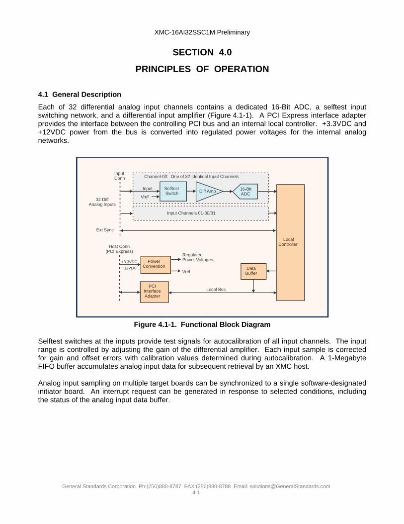
PRINCIPLES OF OPERATION 4.1 General Description
Each of 32 differential analog input channels contains a dedicated 16-Bit ADC, a selftest input switching network, and a differential input amplifier (Figure 4.1-1). A PCI Express interface adapter provides the interface between the controlling PCI bus and an internal local controller. +3.3VDC and +12VDC power from the bus is converted into regulated power voltages for the internal analog networks.
Figure 4.1-1. Functional Block Diagram
Selftest switches at the inputs provide test signals for autocalibration of all input channels. The input range is controlled by adjusting the gain of the differential amplifier. Each input sample is corrected for gain and offset errors with calibration values determined during autocalibration. A 1-Megabyte FIFO buffer accumulates analog input data for subsequent retrieval by an XMC host. Analog input sampling on multiple target boards can be synchronized to a single software-designated initiator board. An interrupt request can be generated in response to selected conditions, including the status of the analog input data buffer.
PCIInterface Adapter
InputConn
32 DiffAnalog Inputs
DataBuffer
LocalController
Ext Sync
RegulatedPower Voltages
Vref
PowerConversion
Diff Amp 16-Bit ADC
Selftest Switch
Vref
Input
Channel-00: One of 32 Identical Input Channels
Input Channels 01-30/31
Local Bus
Host Conn(PCI Express)
+3.3VDC
+12VDC
XMC-16AI32SSC1M Preliminary
_____________________________________________________________________________ General Standards Corporation Ph:(256)880-8787 FAX:(256)880-8788 Email: [email protected]
4-2
4.2 Analog Inputs
Analog-to-digital conversions can be performed on signals from any of several sources, which are selected by the selftest switches shown in Figure 4.1-1. During normal operation, the ADC's receive system analog input signals from the input connector. For selftest and autocalibration operations, the internal voltage reference can be routed through the selftest switches to the ADC.
Serial data from all ADCs are deserialized simultaneously and then multiplexed into a parallel data pipeline within the local controller. The output of the multiplexer passes through a digital processor that applies gain and offset correction values obtained during autocalibration. The corrected data is then formatted and loaded into the analog input data buffer.
The inputs can be acquired either continuously or in discrete bursts. Burst triggers can be obtained from various sources, including an external Sync input I/O pin or by a 16-bit divider driven by the internal master clock. The number of samples in a burst is controlled by a Burst Size register. 4.3 Rate Generators
The local controller contains two independent rate generators, A and B, each of which divides a master clock frequency by a software-controlled 16-bit integer. The Rate-A generator provides the input sample clock by default, and the Rate-B generator usually is dedicated to generating triggered-burst triggers. The generators can be cascaded to produce very long sampling or burst intervals. 4.4 Data Buffer
A 1M-Byte FIFO buffer accumulates analog input data for subsequent retrieval by the PCI Express bus. The buffer is supported by a 'size' register that tracks the number of values in the buffer, and by a threshold flag that can be used to generate an interrupt request when the number of values in the buffer moves above or below a selected count. Local data packing is supported for 16-bit data, and DMA transfers can be implemented in both block and demand modes. 4.5 Autocalibration
Autocalibration is an embedded firmware utility that calibrates all analog input channels to a single internal voltage reference. The utility can be invoked at any time by the application software.
An internal voltage reference is used to calibrate the span of each channel, and a zero-reference is used to calibrate the offset value. Correction values determined during autocalibration are applied to each digitized sample as it is acquired during acquisition, and are retained until the autocalibration sequence is repeated, or until power is removed. 4.6 Power Control
Regulated supply voltages of ±5 VDC and ±15 VDC are required for internal analog networks, and are derived from the +3.3-Volt and +12-Volt inputs provided by the PCI Express bus, both by switching preregulators and by linear postregulators.
XMC-16AI32SSC1M Preliminary
____________________________________________________________________________ General Standards Corporation Ph:(256)880-8787 FAX:56)880-8788 Email: [email protected]
A-1
APPENDIX A
Local Control Register Quick Reference
XMC-16AI32SSC1M Preliminary
____________________________________________________________________________ General Standards Corporation Ph:(256)880-8787 FAX:56)880-8788 Email: [email protected]
A-2
APPENDIX A Local Control Register Quick Reference
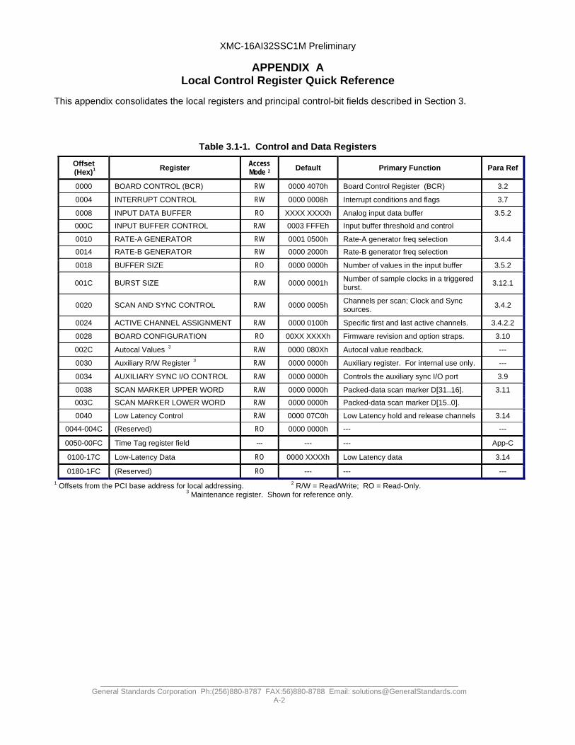
This appendix consolidates the local registers and principal control-bit fields described in Section 3.
Table 3.1-1. Control and Data Registers
Offset (Hex)1
Register Access Mode 2 Default Primary Function Para Ref
0000 BOARD CONTROL (BCR) RW 0000 4070h Board Control Register (BCR) 3.2
0004 INTERRUPT CONTROL RW 0000 0008h Interrupt conditions and flags 3.7
0008 INPUT DATA BUFFER RO XXXX XXXXh Analog input data buffer 3.5.2
000C INPUT BUFFER CONTROL R/W 0003 FFFEh Input buffer threshold and control
0010 RATE-A GENERATOR RW 0001 0500h Rate-A generator freq selection 3.4.4
0014 RATE-B GENERATOR RW 0000 2000h Rate-B generator freq selection
0018 BUFFER SIZE RO 0000 0000h Number of values in the input buffer 3.5.2
001C BURST SIZE R/W 0000 0001h Number of sample clocks in a triggered burst.
3.12.1
0020 SCAN AND SYNC CONTROL R/W 0000 0005h Channels per scan; Clock and Sync sources.
3.4.2
0024 ACTIVE CHANNEL ASSIGNMENT R/W 0000 0100h Specific first and last active channels. 3.4.2.2
0028 BOARD CONFIGURATION RO 00XX XXXXh Firmware revision and option straps. 3.10
002C Autocal Values 3 R/W 0000 080Xh Autocal value readback. ---
0030 Auxiliary R/W Register 3 R/W 0000 0000h Auxiliary register. For internal use only. ---
0034 AUXILIARY SYNC I/O CONTROL R/W 0000 0000h Controls the auxiliary sync I/O port 3.9
0038 SCAN MARKER UPPER WORD R/W 0000 0000h Packed-data scan marker D[31..16]. 3.11
003C SCAN MARKER LOWER WORD R/W 0000 0000h Packed-data scan marker D[15..0].
0040 Low Latency Control R/W 0000 07C0h Low Latency hold and release channels 3.14
0044-004C (Reserved) RO 0000 0000h --- ---
0050-00FC Time Tag register field --- --- --- App-C
0100-17C Low-Latency Data RO 0000 XXXXh Low Latency data 3.14
0180-1FC (Reserved) RO --- --- ---
1 Offsets from the PCI base address for local addressing. 2 R/W = Read/Write; RO = Read-Only. 3 Maintenance register. Shown for reference only.
XMC-16AI32SSC1M Preliminary
____________________________________________________________________________ General Standards Corporation Ph:(256)880-8787 FAX:56)880-8788 Email: [email protected]
A-3
Table 3.2-1. Board Control Register (BCR)
Offset: 0000h Default: 0000 4070h
Bit Mode Designation Def Description Para Ref
D00-D02 R/W AIM[2..0] 0 Analog input mode. Selects system inputs or selftest mode. Defaults to System Inputs
3.5.3.1
D03 R/W (Reserved) 0 --- ---
D04-D05 R/W RANGE[1..0] 3h Analog input range. Defaults to ±10V range. 3.4.1
D06 R/W OFFSET BINARY 1 Selects offset-binary analog I/O data format when asserted HIGH, or two's complement when LOW. 3.5.1.2
D07-D9 R/W (Reserved) 0h --- ---
D10 RO DATA ON HOLD 0 Low-Latency access status flag. 3.14
D11 R/W DISABLE SCAN MARKER 0 Disables the scan marker in data packing mode. 3.11
D12 R/W *INPUT SYNC 0
Produces a single ADC clock when selected in the Scan and Sync Control Register, or a single burst trigger when selected with the Burst On Sync control field.
3.12
D13 R/W *AUTOCAL 0 Initiates an autocalibration operation when asserted. 3.6
D14 RO AUTOCAL PASS 1 Set HIGH at reset or autocal initialization. A HIGH state after autocal completion confirms a successful calibration.
D15 R/W *INITIALIZE 0 Initializes the board when set HIGH. Sets all register defaults. 3.3
D16 R/W BUFFER UNDERFLOW 0 Set HIGH if the buffer is read while empty. Cleared by direct write or by buffer clear. 3.5.2
D17 R/W BUFFER OVERFLOW 0 Set HIGH if the buffer is written to when full. Cleared by direct write or by buffer clear.
D18 R/W ENABLE DATA PACKING 0 Enables local-bus data packing 3.11
D19 R/W (Reserved) 0 --- ---
D20 R/W ENABLE TIME TAG OPERATION 0 Enables time tagging operations. c1.1
D21-D31 RO (Reserved) 0 --- ---
* Clears automatically when the associated operation is completed.
Table 3.4-1. Analog Voltage Range Selection (BCR field)
Range Select[1:0] Analog Input Range
0 ±1.25V
1 ±2.5V
2 ±5 Volts
3 ±10 Volts

XMC-16AI32SSC1M Preliminary
____________________________________________________________________________ General Standards Corporation Ph:(256)880-8787 FAX:56)880-8788 Email: [email protected]
A-4
Table 3.4-2. Scan and Sync Control Register
Offset: 0020h Default: 0000 0005h
Bit Mode Designation Def Description
D00-D02 R/W ACTIVE CHANNELS 5h
Number of active input channels:
0 => Single-Channel mode * 1 => 2 channels (00-01) 2 => 4 channels (00-03) 3 => 8 channels (00-07) 4 => 16 channels (00-15) 5 => 32 channels (00-31); Default value 6 => (Reserved) 7 => Channel group assignment (See Section 3.4.2.2) * Channel selected by Single-Channel Select field below.
D03-D04 R/W SAMPLE CLOCK SOURCE 0h
Selects the analog input sample clocking source and I/O mode: 0 => External Clock input line (Selects Clock TARGET mode) 1 => Internal Rate-A generator output 2 => Internal Rate-B generator output 3 => BCR Input Sync control bit (If bursting disabled)
D05 R/W ENABLE CLOCKING 0 Enables the selected ADC clocking process
D06 R/W RATE-B SYNC OUTPUT 0
Provides the output of the Rate-B generator as an external output pulse, and drives the Rate-B generator either from the output of the Rate-A generator or from the sample clock. Over-rides the Burst-On-Sync selection. See 3.15.
D07 RO BURST BUSY 0 Indicates that a triggered burst is in progress.
D08-D09 R/W BURST ON SYNC 0h
Selects bursting trigger source and I/O mode (Section 3.12) 0 => Bursting disabled 1 => Rate-B generator 2 => External Sync-I/O input (Selects Sync TARGET mode) 3 => BCR Input Sync control bit.
D10 R/W RATE-B CLOCK SOURCE 0 Selects the clock input source for the Rate-B generator: 0 => Master clock (or Sample Clock; See 3.15). 1 => Rate-A generator output.
D11 R/W INVERT CLOCK AND SYNC I/O 0 Inverts the logic polarities of external clock and sync I/O input and output signals to assert HIGH.
D12-17 R/W SINGLE-CHANNEL SELECT 0h Selects the input channel number when operating in the Single-Channel scanning mode.
D18-D31 RO (Reserved) 0 Inactive
Table 3.4-3. Active Channel Assignment
Offset: 0000 0024h Default: 0000 0100h
Data Bit Mode Designation Default Description
D00-D07 R/W FIRST CHANNEL SELECT 0 First (lowest-numbered) active channel
D08-D15 R/W LAST CHANNEL SELECT 1 Last (highest-numbered) active channel
D16-D31 RO (Reserved) 0 Inactive. Returns all-zero.

XMC-16AI32SSC1M Preliminary
____________________________________________________________________________ General Standards Corporation Ph:(256)880-8787 FAX:56)880-8788 Email: [email protected]
A-5
Table 3.4-4. Rate Generator Register
Offset: 0010h (Rate-A), 0014h (Rate-B) Default: 0001 0500h (Rate-A), 0000 2000h (Rate-B)
Data Bit Mode Designation Default Description
D00-D15 R/W NRATE --- Rate generator frequency control
D16 R/W GENERATOR DISABLE 1 Disables the rate generator when HIGH
D17-D31 RO (Inactive) 0 ---
Table 3.4-5. Rate Generator Frequency Selection
Nrate ( RATE[15..0] ) Fgen
with 64 MHz Master Clock
(Dec) (Hex) (Hz, or Samples per second: SPS )
64 40 1,000,000
1280 500 50,000
--- --- Fgen (Hz) = 64,000,000 / Nrate
Table 3.5-1. Input Data Buffer; Nonpacked Data Offset: 0008h Default: N/A
Channel-00 Tag Reserved * (Zero) Channel Data Value
Data Bit(s) D[31] D[30..16] D[15..0]
All fields are read-only; Write-data is ignored.
Table 3.5-2. Input Data Coding
16-Bit Digital Value (Hex)
Analog Input Level Offset Binary Two's Complement
Positive Full Scale minus 1 LSB FFFF 7FFF
Zero (Midscale) 8000 0000
Zero minus 1 LSB 7FFF FFFF
Negative Full Scale 0000 8000

XMC-16AI32SSC1M Preliminary
____________________________________________________________________________ General Standards Corporation Ph:(256)880-8787 FAX:56)880-8788 Email: [email protected]
A-6
Table 3.5-3. Input Data Buffer Control Register Offset: 000Ch Default: 0003 FFFEh
Data Bit Mode Designation Def Description
D00-D17 R/W THRESHOLD VALUE 3 FFFEh Input buffer threshold value.
D18 R/W CLEAR BUFFER * 0 Clears (empties) the input buffer and processing pipeline when asserted HIGH.
D19 RO THRESHOLD FLAG 0 Asserted HIGH when the number of values in the input buffer exceeds the THRESHOLD VALUE.
D20-D31 RO (Inactive) 0 ---
*Clears automatically.
Table 3.5-4. Buffer Size Register Offset: 0018h Default: 0000 0000h
Data Bit Mode Designation Def Description
D00-D18 RO BUFFER SIZE 00000h Number of locations occupied in the input buffer
D19-D31 RO (Inactive) 0 ---
Table 3.5-5. Analog Input Function Selection (BCR field)
AIM[2:0] Function or Mode
0 System analog input mode (Default mode).
1 (Reserved)
2 ZERO test. Internal ground reference is connected to all analog input channels.
3 +VREF test. Internal voltage reference is connected to all analog input channels.
4-7 (Reserved)

XMC-16AI32SSC1M Preliminary
____________________________________________________________________________ General Standards Corporation Ph:(256)880-8787 FAX:56)880-8788 Email: [email protected]
A-7
Table 3.7-1. Interrupt Control Register
Offset: 0000 0004h Default: 0000 0008h
Data Bit Mode Designation Def Value Interrupt Event
D00-02 R/W IRQ0 A0,1,2 0 0 Initialization completed.
1 Autocalibration operation completed
2 Input sample initiated (Sync)
3 Input sample completed (data ready)
4 Triggered burst initiated (BURST BUSY => HI)
5 Triggered burst completed (BURST BUSY => LO)
6-7 (Reserved)
D03 R/W IRQ0 REQUEST 1* --- Group 0 interrupt request flag. Set HIGH when the selected interrupt condition occurs. Clears the request when cleared LOW by the bus.
D04-06 R/W IRQ1 A0,1 0 0 Idle; no interrupt condition selected.
1 Input buffer threshold LOW-HIGH transition
2 Input buffer threshold HIGH-LOW transition
3 Input buffer overflow or underflow
4-7 (Reserved)
D07 R/W IRQ1 REQUEST 0 --- Group 1 interrupt request flag. See D03.
D08-31 RO (Inactive) 0 ---
* HIGH after reset.
Table 3.9-1. Auxiliary Sync I/O Control
Offset: 0000 0034h Default: 0000 0000h
Data Bit Mode Designation Default Description
D00-01 R/W AUX CLOCK Control Mode 0 AUX CLOCK I/O Control Mode: 0 => Inactive 1 => Active Input (LO-to-HI edge) 2 => Active Output (Positive pulse) 3 => (Reserved)
D02-03 R/W AUX SYNC Control Mode 0 AUX SYNC I/O Control Mode *
D04-05 R/W (Reserved) 0 ---
D06-07 R/W (Reserved) 0 ---
D08 R/W INVERT INPUTS 0 Active inputs are detected on the LO-to-HI edge when this bit is LOW, or on the HI-to-LO edge when this bit is HIGH.
D09 R/W INVERT OUTPUTS 0 Active outputs produce HIGH pulses when this bit is LOW, or LOW pulses when this bit is HIGH.
D10 R/W NOISE SUPPRESSION ** 0 When LOW, input debounce time is 85ns-110ns and output pulse width is 135ns. When HIGH, input debounce time is 1.5us, and output pulse width is 2.0us.
D11-31 RO (Reserved) 0 Read-back as all-zero.
* Same configuration as the AUX CLOCK I/O control mode. ** Ignored for sync outputs if operating in Rate-B Sync Output mode. See 3.15

XMC-16AI32SSC1M Preliminary
____________________________________________________________________________ General Standards Corporation Ph:(256)880-8787 FAX:56)880-8788 Email: [email protected]
A-8
Table 3.10-1. Board Configuration Register
Offset: 0000 0028h Default: 00XX XXXXh
Bit Field Description
D00-D11 Firmware Revision
D12-D15 (Reserved status flags or revision field).
D16-D17
Channel Availability: 0 => 32 Channels 1 => 16 Channels 2 => (Reserved) 3 => (Reserved)
D18-D19 Master Clock Frequency: 0 => 64.000 MHz 1-3 => (Reserved)
D20-D21 Custom Feature: 0-3 => (Reserved)
D22-D31 (Reserved)
Table 3.11-1. Data Packing
Buffer Data Field
ENABLE DATA PACKING = 0 DISABLE SCAN MARKER = X
ENABLE DATA PACKING = 1 DISABLE SCAN MARKER = 0
ENABLE DATA PACKING = 1 DISABLE SCAN MARKER = 1
Buffer Lword Order
D[31..16] D[15..0] D[31..16] D[15..0] D[31..16] D[15..0]
00 8000h Chan 00 Data Upper Marker Lower Marker Chan 01 Data Chan 00 Data
01 0000h Chan 01 Data Chan 01 Data Chan 00 Data Chan 03 Data Chan 02 Data
02 0000h Chan 02 Data Chan 03 Data Chan 02 Data Chan 05 Data Chan 04 Data
03 0000h Chan 03 Data Chan 05 Data Chan 04 Data Chan 07 Data Chan 06 Data
--- --- --- --- --- --- ---
Table 3.12-1. Burst Trigger Source
Scan and Sync Register
BURST ON SYNC Burst Trigger Source Sync I/O Pin
0 Bursting disabled. Input (Disabled)
1 Rate-B generator. Trigger Output
2 External Sync I/O input pin (or AUX input) Trigger Input (Target mode)
3 INPUT SYNC control bit in the BCR. Trigger Output
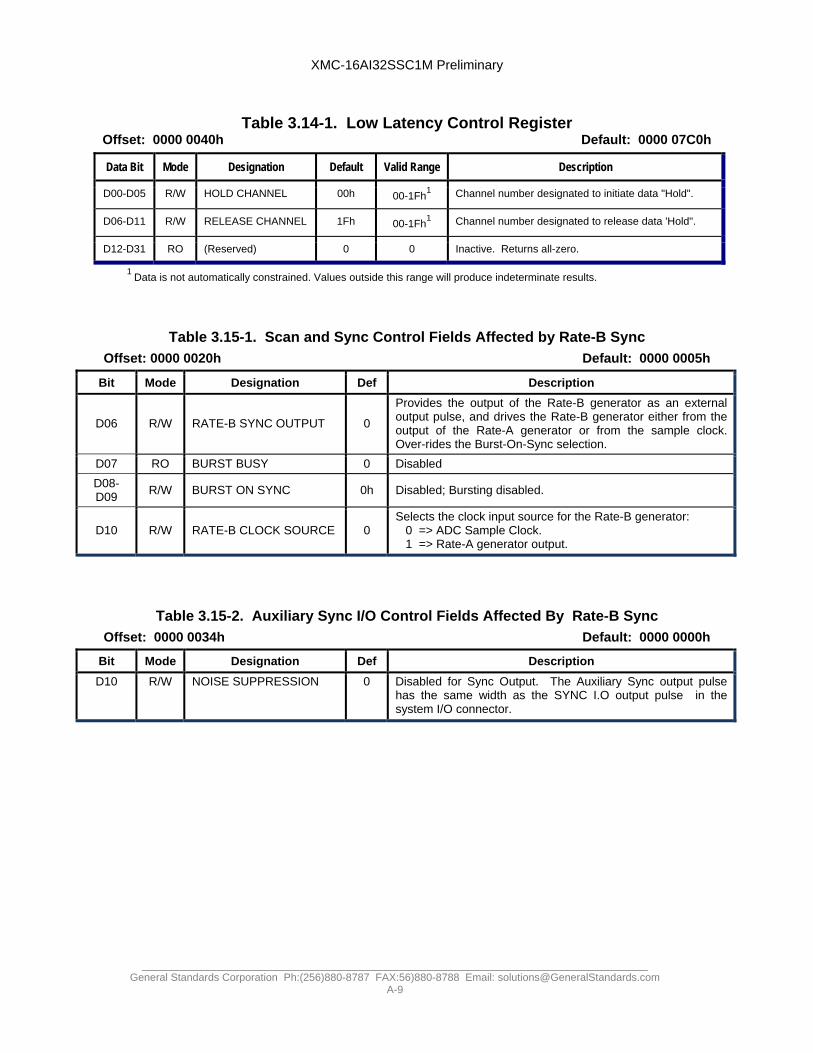
XMC-16AI32SSC1M Preliminary
____________________________________________________________________________ General Standards Corporation Ph:(256)880-8787 FAX:56)880-8788 Email: [email protected]
A-9
Table 3.14-1. Low Latency Control Register Offset: 0000 0040h Default: 0000 07C0h
Data Bit Mode Designation Default Valid Range Description
D00-D05 R/W HOLD CHANNEL 00h 00-1Fh1
Channel number designated to initiate data "Hold".
D06-D11 R/W RELEASE CHANNEL 1Fh 00-1Fh1
Channel number designated to release data 'Hold".
D12-D31 RO (Reserved) 0 0 Inactive. Returns all-zero.
1 Data is not automatically constrained. Values outside this range will produce indeterminate results.
Table 3.15-1. Scan and Sync Control Fields Affected by Rate-B Sync
Offset: 0000 0020h Default: 0000 0005h
Bit Mode Designation Def Description
D06 R/W RATE-B SYNC OUTPUT 0
Provides the output of the Rate-B generator as an external output pulse, and drives the Rate-B generator either from the output of the Rate-A generator or from the sample clock. Over-rides the Burst-On-Sync selection.
D07 RO BURST BUSY 0 Disabled
D08-D09
R/W BURST ON SYNC 0h Disabled; Bursting disabled.
D10 R/W RATE-B CLOCK SOURCE 0 Selects the clock input source for the Rate-B generator: 0 => ADC Sample Clock. 1 => Rate-A generator output.
Table 3.15-2. Auxiliary Sync I/O Control Fields Affected By Rate-B Sync
Offset: 0000 0034h Default: 0000 0000h
Bit Mode Designation Def Description
D10 R/W NOISE SUPPRESSION 0 Disabled for Sync Output. The Auxiliary Sync output pulse has the same width as the SYNC I.O output pulse in the system I/O connector.

XMC-16AI32SSC1M Preliminary
____________________________________________________________________________ General Standards Corporation Ph:(256)880-8787 FAX:(256)880-8788 Email: [email protected]
B-1
APPENDIX B
Migration From PMC66-16AI32SSC

XMC-16AI32SSC1M Preliminary
____________________________________________________________________________ General Standards Corporation Ph:(256)880-8787 FAX:(256)880-8788 Email: [email protected]
B-2
Appendix B
Migration from PMC66-16AI32SSC
Operation of the XMC-16AI32SSC1M is very similar to that of the PMC66-16AI32SSC. This appendix summarizes the principal similarities and differences between the two products, and is provided as a general guide rather than a definitive list of requirements. B.1. Comparison of Features
Table B.1 provides a brief comparison of PMC66-16AI32SSC and XMC-16AI32SSC1M features.
Table B.1. PMC66-16AI32SSC, XMC-16AI32SSC1M Features Comparison
Feature PMC66-16AI32SSC XMC-16AI32SSC1M
Number of Input Channels 32 32
Conversion Resolution 16 Bits 16 Bits
Native Input Configuration Differential Differential
Input Ranges ±10V, ±5V, ±2.5V ±10V, ±5V, ±2.5V, 1.25V
Sample Rates 0-200KSPS 0-1MSPS
Time Stamp Yes, Optional Yes, Standard
Low Latency Yes, Optional Yes, Standard
Host Interface * PCI 2.3; D32; 33MHz/66MHz PCI Express, Single lane
* The host adapter (PEX-8311) provides the same local interface for both the XMC-16AI32SSC1M and PMC66-16AI32SSC products, thereby assuring a transparent software-control transition from PMC66-16AI32SSC to XMC-12AI32SSC1M.
B.2. Migration Issues
General:
1. The maximum sample rate has increased from 200KSPS to 1MSPS. 2. Low-Latency and Time-Tagging functions are now standard features. 3. The number of input ranges has increased from three to four.
Section 2.0. Installation and Maintenance: Table 2.2-1: Two sets of system pin assignments (a) and (b) have been replaced with a single compatible standard assignment. Four pins now have software-configured contexts.
Section 3.0. Control Software:
Tables 3.1-1 and 3.4-1: BCR 'Range' field and default value have changed to accommodate an additional input range.
Paragraph 3.4.4.2, Table 3.4-5: The maximum sample rate has increased to 1MSPS. The master clock frequency is now 64MHz.
Table 3.10-1: Production options reflect functional changes.
Paragraph 3.14: Added low latency control register.

XMC-16AI32SSC1M Preliminary
_____________________________________________________________________________ General Standards Corporation Ph:(256)880-8787 FAX:(256)880-8788 Email: [email protected]
APPENDIX C
Time Tagging Operations
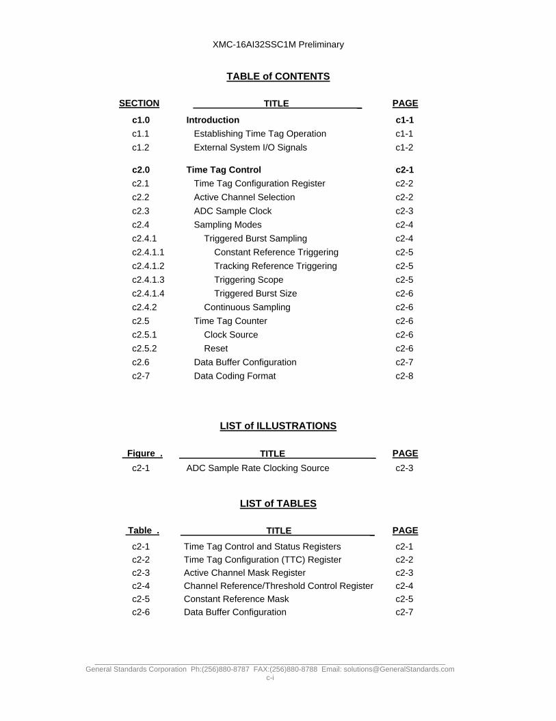
XMC-16AI32SSC1M Preliminary
_____________________________________________________________________________ General Standards Corporation Ph:(256)880-8787 FAX:(256)880-8788 Email: [email protected]
c-i
TABLE of CONTENTS
SECTION TITLE PAGE
c1.0 Introduction c1-1
c1.1 Establishing Time Tag Operation c1-1
c1.2 External System I/O Signals c1-2
c2.0 Time Tag Control c2-1
c2.1 Time Tag Configuration Register c2-2
c2.2 Active Channel Selection c2-2
c2.3 ADC Sample Clock c2-3
c2.4 Sampling Modes c2-4
c2.4.1 Triggered Burst Sampling c2-4
c2.4.1.1 Constant Reference Triggering c2-5
c2.4.1.2 Tracking Reference Triggering c2-5
c2.4.1.3 Triggering Scope c2-5
c2.4.1.4 Triggered Burst Size c2-6
c2.4.2 Continuous Sampling c2-6
c2.5 Time Tag Counter c2-6
c2.5.1 Clock Source c2-6
c2.5.2 Reset c2-6
c2.6 Data Buffer Configuration c2-7
c2-7 Data Coding Format c2-8
LIST of ILLUSTRATIONS
Figure . TITLE PAGE
c2-1 ADC Sample Rate Clocking Source c2-3
LIST of TABLES
Table . TITLE PAGE
c2-1 Time Tag Control and Status Registers c2-1
c2-2 Time Tag Configuration (TTC) Register c2-2
c2-3 Active Channel Mask Register c2-3
c2-4 Channel Reference/Threshold Control Register c2-4
c2-5 Constant Reference Mask c2-5
c2-6 Data Buffer Configuration c2-7

XMC-16AI32SSC1M Preliminary
_____________________________________________________________________________ General Standards Corporation Ph:(256)880-8787 FAX:(256)880-8788 Email: [email protected]
c-ii
XMC-16AI32SSC1M Preliminary
_____________________________________________________________________________ General Standards Corporation Ph:(256)880-8787 FAX:(256)880-8788 Email: [email protected]
c1-1
APPENDIX C
TIME TAGGING OPERATIONS c1.0 Introduction
Time tagging permits analog input data to be referenced to a software-controlled timebase. In this implementation, the timebase is represented by a 48-Bit time tag counter that is clocked or advanced by a 1.0 microsecond reference clock. The accumulated time tag count can be appended to an input data block as a header that contains the time tag count, as well as additional information pertaining to the size and structure of the data block. NOTE: This appendix applies only if the ENABLE TIME TAG OPERATION control bit is
asserted HIGH in the BCR (Table 3.2-1).
c1.1 Establishing Time Tag Operation
The Time Tag Operational mode is established by setting the ENABLE TIME TAG OPERATION control bit HIGH in the BCR shown in Table 3.2-1. When the time-tag operational mode is established, a block of registers dedicated to time tag operations extends the original register set described in Section 3 of this manual. The operations described in this appendix are applicable only when this control bit is HIGH. If the ENABLE TIME TAG OPERATION control bit is LOW, then this appendix does not apply, and all operations contained in Section 3 are in effect. NOTE: While the time tag operational mode is enabled, the descriptions contained in this appendix
supersede those for equivalent operations described in Section 3. When the time-tag operational mode is enabled, the following control registers and control fields in the original register set described in Section-3 are ignored, and their functions are either omitted or replaced with equivalent time tag control registers.
Board Control Register (BCR); Table 3.2-1:
DISABLE SCAN MARKER INPUT SYNC ENABLE DATA PACKING.
Rate-B Generator; Paragraph 3.4.4.
Burst Size Control Register; Paragraph 3.12.
Scan and Sync Control Register; Table 3.4-2.
Active Channel Assignment; Paragraph 3.4.2.2.
Auxiliary Sync I/O Control; Paragraph 3.9.
Scan Marker Upper Word; Paragraph 3.11.
Scan Marker Lower Word; Paragraph 3.11.

XMC-16AI32SSC1M Preliminary
_____________________________________________________________________________ General Standards Corporation Ph:(256)880-8787 FAX:(256)880-8788 Email: [email protected]
c1-2
c1.2 External System I/O Signals
The following pins in the system I/O connector are associated with Time Tag operations:
A40: CLOCK RST INP (input), B36: REF CLK INP (input), B38: SAMP CLK INP (input), B40: SAMP CLK OUT (output).
Logic levels for both inputs and outputs are low-voltage TTL (LVTTL). All signals are asserted HIGH and pulled up internally to +3.3V through 33K.

XMC-16AI32SSC1M Preliminary
_____________________________________________________________________________ General Standards Corporation Ph:(256)880-8787 FAX:(256)880-8788 Email: [email protected]
c2-1
c2.0 Time Tag Control
Time tag operations are controlled by the register set shown in Table c2-1. These registers represent an extension of the original field of control registers described in Section 3 of this manual, and are active only when operating in the Time Tag mode. The Time Tag Operational mode is invoked by setting the ENABLE TIME TAG OPERATION control bit HIGH in the BCR.
Table c2-1. Time Tag Control and Status Registers
Offset (Hex) 1
Register Mode Default Primary Function Ref
0050 TIME TAG CONFIGURATION (TTC) RW 0000 0000h Primary control register for time-tag operations. c2.1
0054 ACTIVE CHANNEL MASK R/W FFFF FFFFh Active channel selection mask. c2.2
0058 TIME TAG COUNTER LOWER RO XXXX XXXXh Time tag counter lower 32 bits. c2.5
005C TIME TAG COUNTER UPPER RO 0000 XXXXh Time tag counter upper 16 bits. c2.5
0060 TIME TAG RATE DIVIDER R/W 0000 0002h Rate divider Nrate_timetag for ADC clocking. Minimum valid value = 2. c2.3
0064 BURST SIZE R/W 0000 0001h Number of samples acquired per channel after a trigger occurs. c2.4.1.4
0068 CONSTANT REFERENCE MASK R/W 0000 0000h Selects 'constant' or 'automatically updated' reference values individually for each input channel.
c2.4.1.1
006C-
007C (Reserved) RO 0000 0000h --- ---
0080 CHAN00_THRESHOLD/REFERENCE R/W 4000 8000h Reference (D00-15) and Threshold (D16-31) c2.4.1
0084 CHAN01_THRESHOLD/REFERENCE R/W 4000 8000h values assigned to each input channel.
0088 CHAN02_THRESHOLD/REFERENCE R/W 4000 8000h
008C-
00F8
CHAN03_THRESHOLD/REFERENCE to CHAN30_THRESHOLD/REFERENCE
R/W 4000 8000h (Offset = 0080h + 4*Channel Number)
00FC CHAN31_THRESHOLD/REFERENCE R/W 4000 8000h
1 Offset from the PCI base address for local addressing.

XMC-16AI32SSC1M Preliminary
_____________________________________________________________________________ General Standards Corporation Ph:(256)880-8787 FAX:(256)880-8788 Email: [email protected]
c2-2
c2.1 Time Tag Configuration Register (TTC)
Primary control of time tag operations takes place through the Time Tag Configuration (TTC) register shown in Table c2-2.
Table c2-2. Time Tag Configuration (TTC) Register
Offset: 0050h Default: 0000 0000h
Bit Mode Designation Def Description Ref
D00-01 R/W ADC SAMPLE CLOCK SOURCE 0
Selects the source of the ADC sample clock: 0 => Internal Rate-A generator. 1 => External 'SAMP CLK INP' input line. 2 => External 'REF CLK INP' input line. 3 => (Reserved).
c2.3
D02 R/W ENABLE ADC CLOCKING 0 Enables ADC sampling when HIGH. Disables sampling when LOW. c2.4
D03 R/W (Reserved) 0 --- ---
D04 R/W ENABLE REFERENCE TRIGGERING 0 Selects the reference-triggered mode when HIGH, or the free-running mode when LOW. c2.4
D05 R/W (Reserved) 0 --- ---
D06 R/W GLOBAL TRIGGERING 0 All active channels are logged after each trigger when this bit is HIGH, but only triggered channels are logged when LOW.
c2.4.1.3
D07 R/W (Reserved) 0 --- ---
D08 R/W EXTERNAL REFERENCE CLOCK 0
Selects the external 'REF CLK INP' input line as the time-tag reference clock source when HIGH, or the internal rate generator when LOW.
c2.5.1
D09 R/W RESET TIME TAG * 0 Unconditionally clears the time tag counter to zero when set HIGH. c2.5.2
D10 R/W EXTERNAL TIME TAG RESET 0 Selects the external input line 'CLOCK RST INP' as the source of the time tag counter reset when HIGH.
c2.5.2
D11 R/W ENABLE TIME TAGGING 0
The time tag header is inserted when this bit is HIGH, or is omitted when LOW. Applies in all modes when the time-tag operational mode is invoked.
c2.6
D12-31 RO (Reserved) 0 --- ---
* Does not clear automatically. Not edge-detected. Must be written LOW.
c2.2 Active Channel Selection
The Active Channel Mask control register shown in Table c2-3 determines which input channels will be acquired or ignored during an acquisition sequence. A channel is designated as active by setting the corresponding ACQUIRE CHANNEL xx control bit HIGH, or as inactive by clearing the bit LOW. Active channels are sampled and logged into the data buffer during acquisition, while inactive channels are ignored and do not occupy space in the buffer.

XMC-16AI32SSC1M Preliminary
_____________________________________________________________________________ General Standards Corporation Ph:(256)880-8787 FAX:(256)880-8788 Email: [email protected]
c2-3
Table c2-3. Active Channel Mask Register Offset: 0054h Default: FFFF FFFFh
Bit Mode Designation Def Description
D00 R/W ACQUIRE CHANNEL 00 1 Each bit enables Channel_XX acquisition when set HIGH;
D01 R/W ACQUIRE CHANNEL 01 1 or disables Channel_XX acquisition when cleared LOW.
D02 R/W ACQUIRE CHANNEL 02 1
D03-29 R/W ACQUIRE CHANNEL 03-29 1 (Control-Bit number equals channel number)
D30 R/W ACQUIRE CHANNEL 30 1
D31 R/W ACQUIRE CHANNEL 31 1
c2.3 ADC Sample Clock
The ADC conversion sample clock can be obtained from any of the three sources listed in Table c2.2 under ADC SAMPLE CLOCK SOURCE. Setting this field to equal '1' or '2', selects the external SAMP CLK INP or REF CLK INP input pin respectively, as the source of the ADC sample clock. If the ADC SAMPLE CLOCK SOURCE control field equals '0' (default), then the internal Rate-A generator supplies the sample clock. The ADC sample rate Fsamp (Figure c2-1) is determined by the master clock frequency Fclk, and two integers Nrate_A and Nrate_timetag as:
Fsamp = Fclk / (Nrate_A * Nrate_timetag). Nrate_A is the value contained in the control register RATE-A GENERATOR shown in Table 3.4-4, and Nrate_timetag is the 20-Bit value in the TIME TAG RATE DIVIDER control register listed in Table c2.1. Fclk has a standard value of 64.000MHz, although other frequencies are available; see Table 3.10-1. With a 64MHz master clock frequency, the range of sample rates available with the Rate-A generator is 0.015Hz to 1.0MHz, in which the upper limit is determined by the A/D converters. The minimum value for Nrate_A and Nrate_timetag is 2.
Figure c2-1. ADC Sample Rate Clock Source
Gen A
Nrate-A
Master ClockFgen-A
Nrate-Timetag
SAMP CLK INP
REF CLK INPTime Tag
Rate Divider
I/O Conn
Fgen-div
ADC SampleClock Source
SAMP CLK OUT
ADCSample Rate
Fsamp

XMC-16AI32SSC1M Preliminary
_____________________________________________________________________________ General Standards Corporation Ph:(256)880-8787 FAX:(256)880-8788 Email: [email protected]
c2-4
For a 64MHz master clock frequency, Fsamp is:
Fsamp (kHz) = 64,000 / (Nrate_A * Nrate_timetag).
For example, Nrate_A and Nrate_timetag values of 2 and 1000 respectively would produce an ADC clocking frequency of 32.000kHz. NOTE: The Rate-A generator can be disabled with a control bit in the associated control
register (Table 3.4-4). This 'disable' control bit must be LOW in order for the internal rate generator to function.
If REF CLK INP is selected as the clock source, the ADC sample rate Fsamp equals the frequency of the selected source divided by the 20-Bit integer Nrate-timetag. For the SAMP CLK INP source, the ADC sample rate Fsamp equals the frequency of the source with no division involved, and simplifies the synchronization of ADC conversions on multiple boards.
When the ENABLE ADC CLOCKING control bit is high in the TimeTag Configuration register, the external output pin SAMP CLK OUT provides a 200 nanosecond positive pulse each time an ADC conversion occurs. SAMP CLK OUT is disabled if ENABLE ADC CLOCKING is LOW.
NOTE: For either external clock source input, REF CLK INP or SAMP CLK INP, the minimum time for both HIGH and LOW levels is 100 nanoseconds.
c2.4 Sampling Modes
The analog inputs can be sampled in either a continuous 'free running' mode or in triggered bursts. Triggered Burst sampling is selected when the ENABLE REFERENCE TRIGGERING control bit is HIGH in the TTC register, and Continuous sampling is selected when the control bit is LOW. In the Continuous sampling mode, sampling occurs as long as an active clock source is present and the ENABLE ADC CLOCKING control bit is HIGH. Time tagging can be applied in any sampling mode.
c2.4.1 Triggered Burst Sampling
When Triggered Burst sampling is selected, data is acquired in discrete bursts, and each burst is initiated by a specific Trigger event. A trigger event is determined by the amplitude of the data in each channel 'xx', and by the values of the following two software-assigned parameters:
CHANNELxx Trigger Reference, CHANNELxx Trigger Threshold.
Both of these parameters are 16-Bit integers, and are assigned to each channel as indicated in Table c2-1. The reference and threshold values for each channel are contained in a single CHANxx_THRESHOLD/REFERENCE register (Table c2-4), with the Reference occupying the lower 16 bits and the Threshold occupying the upper 16 bits.
Table c2-4. Channel Reference/Threshold Control Register Offset: 0080h + (4 * Channel Number) Default: 4000 8000h
Bit Mode Designation Def Description
D00-15 R/W CHANNELxx REFERENCE 8000h Channel-XX trigger reference
D16-31 R/W CHANNELxx THRESHOLD 4000h Channel-XX trigger threshold

XMC-16AI32SSC1M Preliminary
_____________________________________________________________________________ General Standards Corporation Ph:(256)880-8787 FAX:(256)880-8788 Email: [email protected]
c2-5
If time tagging is enabled, each sample clock latches the current value of the Time Tag counter for insertion into the buffer data header (c2.6).
NOTE: Trigger events that occur during a triggered burst are ignored. Also, an Interrupt can be generated in response to the initiation or termination of a triggered burst (Table 3.7-1).
c2.4.1.1 Constant Reference Triggering
Constant reference triggering is selected for each input channel by setting the associated CONSTANT REFERENCE VALUE control bit HIGH in the Constant Reference Mask control register (Table c2-5). In this mode, a trigger event occurs when the input data for the channel falls outside the range defined by the Channel Reference, plus or minus the Channel Threshold value. That is; when:
Reference minus Threshold > Channel Trigger Amplitude > Reference plus Threshold,
or: Amplitude < Reference minus Threshold => Trigger, Amplitude > Reference plus Threshold => Trigger. While Constant Reference triggering is selected, the assigned reference value is unaffected by a trigger event.
Because trigger-event detection is performed dynamically on a pipelined data stream, modifying a reference or threshold value during acquisition may cause an erroneous response for the ensuing sample.
Table c2-5. Constant Reference Mask Offset: 0068h Default: 0000 0000h
Bit Mode Designation Def Description
D00 R/W CHAN-00 CONSTANT REFERENCE 0 The Channel-00 Reference value remains unchanged after each trigger when this bit is HIGH, or is updated automatically when LOW to equal the input level.
D01-D31 R/W CHAN 01-31 CONSTANT REFERENCE 0 Same function as Bit D00, applied to Channels 01-31.
c2.4.1.2 Tracking Reference Triggering
If the CONSTANT REFERENCE VALUE control bit is LOW for a channel in the Constant Reference Mask control register, then Tracking Reference triggering is selected for that channel. This mode is identical to the Constant Reference triggering mode, except the reference value is now modified after each trigger event to re-center the triggering window around the trigger amplitude. The reference value is modified to equal the analog input data value. c2.4.1.3 Triggering Scope
If the GLOBAL TRIGGERING control bit is LOW in the TTC register, then only those channels that experience a trigger event will be acquired during the ensuing burst. If the control bit is HIGH, then all active channels will be acquired during the burst, regardless of which channel or channels actually experienced a trigger.
NOTE: Multiple channels may experience a trigger condition simultaneously. In these instances, the data from all triggered channels will appear in the buffer.

XMC-16AI32SSC1M Preliminary
_____________________________________________________________________________ General Standards Corporation Ph:(256)880-8787 FAX:(256)880-8788 Email: [email protected]
c2-6
c2.4.1.4 Triggered Burst Size
The number of samples acquired from each channel during a burst is referred to as a Sample Block, and is determined by the 16-bit Burst Size control register listed in Table c2-1, and by the number of active channels. For Burst-Size values of one or greater, the number of samples acquired from each input channel equals the value in the register. For example, if a burst size of 10 is selected while 16 channels are active during a burst, then the sample block will contain 160 sample values. A Burst-Size of zero produces a burst that runs continuously until stopped, either by disabling the sampling clock or by clearing the ENABLE REFERENCE TRIGGERING control bit. NOTE: A "Sample Block" refers to all data associated with a single burst trigger. That is; all data
acquired within a single burst.
A "Sample Scan" refers to the data acquired from all channels in response to a single sample clock.
c2.4.2 Continuous Sampling
When operating in the continuous 'free running' sampling mode, data is acquired continuously from all active channels as long as the input data buffer is not full, and if a valid sample clock is selected with the ADC SAMPLE CLOCK SOURCE control field in the TTC register. In this mode, input data accumulates in the buffer as shown in Table c2-6, but all active channels are represented. c2.5 Time Tag Counter
The time tag value in the time tag header represents the accumulated count in a 48-bit counter that is advanced once per microsecond by a 1MHz reference clock, and unless reset (c2.5.2), runs continuously while operating in the time-tagging mode. The entire 48-bit value is latched with each ADC sample clock to prevent rollover errors between the upper and lower bit fields in the data buffer header (c2.6). The latched value appears in the time tag header immediately before the ADC data from the associated sample clock, and is accessible also through the Lower and Upper Time-Tag registers listed in Table c2-1.
c2.5.1 Clock Source
The 1MHz reference clock for the time tag counter can be derived from an internal 1MHz generator, or from a 1 MHz external clock source. If the EXTERNAL REFERENCE CLOCK control bit is HIGH in the TTC register, the reference clock is obtained from the REF CLK INP pin in the system I/O connector. If this control bit is LOW, an internal 1 MHz generator provides the reference clock.
c2.5.2 Reset
The time tag counter can be cleared to zero at any time by asserting the RESET TIME TAG control bit in the TTC register, or by performing an initialization (3.3.2). The counter will remain cleared as long RESET TIME TAG is asserted. The counter can be cleared also from an external input through the CLOCK RST INP input pin in the system I/O connector when the EXTERNAL TIME TAG RESET control bit is set HIGH in the TTC register. If this control bit is LOW, the external CLOCK RST INP input is ignored.
XMC-16AI32SSC1M Preliminary
_____________________________________________________________________________ General Standards Corporation Ph:(256)880-8787 FAX:(256)880-8788 Email: [email protected]
c2-7
c2.6 Data Buffer Configuration
A 48-Bit time tag counter provides a time reference for analog input data, and is included in a time tag header that can be appended to data as it is logged into the data buffer described in Section 3.5.1.1. The structure of the header is shown in Table c2-6. The MSB (D31) of the first longword in each header is set HIGH, to indicate the beginning of a new sample scan.
In addition to time tag information, the header also provides the number (Nb) of ADC samples contained in the ensuing sample scan.
The header is appended in any mode if the ENABLE TIME TAGGING control bit is HIGH in the Time Tag Configuration (TTC) register. If ENABLE TIME TAGGING is LOW, then the header is omitted and the buffer accumulates only sampled data with the channel number attached to each sample.
Sampled input data in the buffer commences immediately after the header, with the data value occupying the lower half bits of each longword, and the associated channel number located in the upper half. The Channel-00 flag shown in Table 3.5-1 is not applied when operating in the time-tag operational mode.
Table c2-6. Data Buffer Configuration
Buffer Lword Order
Segment D[31..16] D[15..0]
0000 Header 8000h Time Tag; Lower 16 Bits (D15..0] First Sample Scan
0001 0000h Time Tag; Intermediate 16 Bits (D31..16]
0002 0000h Time Tag; Upper 16 Bits (D47..32]
0003 0000h Nb; Number of ADC samples in first sample scan
0004 Data First channel number First-channel data value
--- Intermediate channel numbers Intermediate channel data values
Nb + 4 Last channel number Last-channel data value
--- Header 8000h Time Tag; Lower 16 Bits (D15..0] Second Sample Scan
--- 0000h Time Tag; Intermediate 16 Bits (D31..16]
0000h Time Tag; Upper 16 Bits (D47..32]
--- 0000h Nb; Number of ADC samples in second sample scan
--- Data First channel number First-channel data value
--- Intermediate channel numbers Intermediate channel data values
--- Last channel number Last-channel data value
--- --- --- --- (Intermediate scans)
--- Header 8000h Time Tag; Lower 16 Bits (D15..0] Last Sample Scan
--- 0000h Time Tag; Intermediate 16 Bits (D31..16]
--- 0000h Time Tag; Upper 16 Bits (D47..32]
--- 0000h Nb; Number of ADC samples in last sample scan
--- Data First channel number First-channel data value
--- Intermediate channel numbers Intermediate channel data values
--- Last channel number Last-channel data value

XMC-16AI32SSC1M Preliminary
_____________________________________________________________________________ General Standards Corporation Ph:(256)880-8787 FAX:(256)880-8788 Email: [email protected]
c2-8
c2.7 Data Coding Format
When operating in the time-tag mode, the data coding format described in Paragraph 3.5.1.2 applies to the 16-Bit channel data values in the Data buffer, and to the 16-Bit Reference and Threshold values listed in Table c2-4.
XMC-16AI32SSC1M Preliminary
_____________________________________________________________________________ General Standards Corporation Ph:(256)880-8787 FAX:(256)880-8788 Email: [email protected]
Revision History:
10-23-2016: Origination as preliminary draft. 11-20-2016: Para 3.4.4, 3.10: Revised master clock frequency to 64MHz. Para 3.14. Simplified Low-Latency data access.
02-08-2017: Para 3.14: Added low latency control register (Table 3.14-1). App-B: Clarified control interface similarities between products.
02-14-2017: Para 2.3.2, c1.2: Clarified Clk/Sync I/O pin functions.
Copyright (C) 2016 General Standards Corp. Additional copies of this manual or other General Standards Co. literature may be obtained from: General Standards Corp. 8302A Whitesburg Dr. Huntsville, Alabama 35802 Telephone: (256) 880-8787 FAX: (256) 880-8788 The information in this document is subject to change without notice. General Standards Corp. makes no warranty of any kind with regard to this material, including, but not limited to, the implied warranties of merchantability and fitness for a particular purpose. Although extensive editing and reviews are performed before release to ECO control, General Standards Corp. assumes no responsibility for any errors that may exist in this document. No commitment is made to update or keep current the information contained in this document. General Standards Corp. does not assume any liability arising out of the application or use of any product or circuit described herein, nor is any license conveyed under any patent rights or any rights of others. General Standards Corp. assumes no responsibility resulting from omissions or errors in this manual, or from the use of information contained herein. General Standards Corp. reserves the right to make any changes, without notice, to this product to improve reliability, performance, function, or design. All rights reserved. No part of this document may be copied or reproduced in any form or by any means without prior written consent of General Standards Corp.

_____________________________________________________________________________ General Standards Corporation Ph:(256)880-8787 FAX:(256)880-8788 Email: [email protected]
Related Documents