Clemson University TigerPrints All eses eses 5-2017 Wireless Energy Transfer Using Resonant Magnetic Induction for Electric Vehicle Charging Application Neelima Dahal Clemson University, [email protected] Follow this and additional works at: hps://tigerprints.clemson.edu/all_theses is esis is brought to you for free and open access by the eses at TigerPrints. It has been accepted for inclusion in All eses by an authorized administrator of TigerPrints. For more information, please contact [email protected]. Recommended Citation Dahal, Neelima, "Wireless Energy Transfer Using Resonant Magnetic Induction for Electric Vehicle Charging Application" (2017). All eses. 2614. hps://tigerprints.clemson.edu/all_theses/2614

Welcome message from author
This document is posted to help you gain knowledge. Please leave a comment to let me know what you think about it! Share it to your friends and learn new things together.
Transcript
Clemson UniversityTigerPrints
All Theses Theses
5-2017
Wireless Energy Transfer Using ResonantMagnetic Induction for Electric Vehicle ChargingApplicationNeelima DahalClemson University, [email protected]
Follow this and additional works at: https://tigerprints.clemson.edu/all_theses
This Thesis is brought to you for free and open access by the Theses at TigerPrints. It has been accepted for inclusion in All Theses by an authorizedadministrator of TigerPrints. For more information, please contact [email protected].
Recommended CitationDahal, Neelima, "Wireless Energy Transfer Using Resonant Magnetic Induction for Electric Vehicle Charging Application" (2017). AllTheses. 2614.https://tigerprints.clemson.edu/all_theses/2614

WIRELESS ENERGY TRANSFER
USING RESONANT MAGNETIC INDUCTION
FOR ELECTRIC VEHICLE CHARGING APPLICATION
A Thesis
Presented to
the Graduate School of
Clemson University
In Partial Fulfillment
of the Requirements for the Degree
Master of Science
Electrical Engineering
by
Neelima Dahal
May 2017
Accepted by:
Dr. Anthony Q. Martin, Committee Chair
Dr. Pingshan Wang
Dr. Harlan B. Russell

ii
ABSTRACT
The research work for this thesis is based on utilizing resonant magnetic induction
for wirelessly charging electric vehicles. The background theory for electromagnetic
induction between two conducting loops is given and it is shown that an RLC equivalent
circuit can be used to model the loops. An analysis of the equivalent circuit is used to show
how two loosely coupled loops can be made to exchange energy efficiently by operating
them at a frequency which is the same as the resonant frequency of both. Furthermore, it
is shown that the efficiency is the maximum for critical coupling (determined by the quality
factors of the loops), and increasing the coupling beyond critical coupling causes double
humps to appear in the transmission efficiency versus frequency spectrum. In the
experiment, as the loops are brought closer together which increases the coupling between
them, doubles humps, as expected from the equivalent circuit analysis is seen. Two models
for wireless energy transfer are identified: basic model and array model. The basic model
consists of the two loosely coupled loops, the transmitter and the receiver. The array model
consists of a 2 x 2 array of the transmitter and three parasites, and the receiver. It is shown
that the array model allows more freedom for receiver placement at the cost of degraded
transmission efficiency compared to the basic model. Another important part of the thesis
is software validation. HFSS-IE and 4NEC2 are the software tools used and the simulation
results for wire antennas are compared against references obtained from a textbook and a
PhD dissertation. It is shown that the simulations agree well with the references and also
with each other.

iii
DEDICATION
This thesis is dedicated to my mother, Pratibha Dahal. Her biggest dream in life
was to earn a Master’s degree but the circumstances surrounding her ever since her birth
were all against her. When she had me, she hoped to see her dreams come true through me,
and I am very glad that I finally have this thesis to dedicate to her.

iv
ACKNOWLEDGEMENT
I would like to thank my advisor, Dr. Anthony Q. Martin for his guidance. I also
want to thank my committee members, Dr. Pingshan Wang and Dr. Harlan B. Russell, for
their service.
I also want to thank my parents, Pratibha Dahal and Pritam Dahal, and my brother
Nilam Dahal for always believing in me. Special thank you to my boyfriend, Jeff Osterberg,
for his constant support and encouragement throughout graduate school. I could not have
done this without him.

v
TABLE OF CONTENTS Page
TITLE PAGE …………………………………………………………………… i
ABSTRACT …………………………………………………………………..... ii
DEDICATION ………………………………………………………………..... iii
ACKNOWLEDGEMENT ……………………………………………………… iv
LIST OF FIGURES …………………………………………………………….. vi
LIST OF TABLES ……………………………………………………………… xix
CHAPTER
1. INTRODUCTION ……………………………………………………… 1
2. BACKGROUND
I. ELECTROMAGNETIC INDUCTION ……………………………… 5
II. EQUIVALENT CIRCUIT …………………………………………… 11
III. TRANSMISSION EFICIENCY ……………….……………….……. 20
3. ANALYTICAL MODEL AND EXPERIMENTAL SETUP ………..…... 24
4. RESULTS AND DISCUSSIONS ………………………………………... 39
5. SOFTWARE VALIDATION
I. HFSS-IE AND 4NEC2 VALIDATION …………………………….. 60
II. HFSS-IE VERSUS 4NEC2 ……………………………………..…… 65
6. CONCLUSIONS ………………………………………………………… 76
REFERENCES ………………………………………………………………...… 79
vi
LIST OF FIGURES
Figure 2.1: Illustration of how electromagnetic induction works using
two conducting circular loops, transmitter and receiver. The
transmitter terminals are connected to an AC voltage source
inV which has an internal impedance of sZ . The magnetic
field created by the transmitter current is represented by the
field lines and the arrows represent the direction of the field.
When the receiver is placed such that it crosses these
magnetic field lines, current is induced in the receiver. The
direction of the current is such that the magnetic field
generated by the induced current opposes the change in the
magnetic flux generated by the transmitter current. The
receiver terminals are connected to a load LoadZ . 10
Figure 2.2: An inductively coupled circuit. The transmitter and the
receiver loops are represented by series RLC circuits. The
transmitter circuit is connected to an AC voltage source inV
whereas the receiver circuit is not. The mutual inductance of
the transmitter and receiver loops is given by T RM k L L
, where k is the coupling coefficient. 12
Figure 2.3: Equivalent transmitter circuit. The effect of the presence of
the coupled receiver circuit is realized by adding an
impedance 2( ) RM Z in series with the transmitter series
RLC circuit. 14
Figure 2.4: Equivalent receiver circuit. The induced emf in the receiver
circuit due to the current IT in the primary circuit is given by
emf TV j MI . 15
Figure 2.5: Transmitter current versus frequency. When there is no
coupling between the transmitter and the receiver, the
current in the transmitter is the same as that of a series RLC
circuit considered by itself. As the coupling coefficient
increases, the transmitter current peak broadens and starts
showing double humps. Further increasing the coupling
coefficient results in more pronounced double humps which
are farther apart. 19
vii
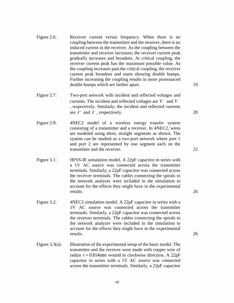
Figure 2.6: Receiver current versus frequency. When there is no
coupling between the transmitter and the receiver, there is no
induced current in the receiver. As the coupling between the
transmitter and receiver increases, the receiver current peak
gradually increases and broadens. At critical coupling, the
receiver current peak has the maximum possible value. As
the coupling increases past the critical coupling, the receiver
current peak broadens and starts showing double humps.
Further increasing the coupling results in more pronounced
double humps which are farther apart. 19
Figure 2.7: Two-port network with incident and reflected voltages and
currents. The incident and reflected voltages are V and V
, respectively. Similarly, the incident and reflected currents
are I and I , respectively. 20
Figure 2.8: 4NEC2 model of a wireless energy transfer system
consisting of a transmitter and a receiver. In 4NEC2, wires
are modeled using short, straight segments as shown. The
system can be studied as a two-port network where port 1
and port 2 are represented by one segment each on the
transmitter and the receiver. 22
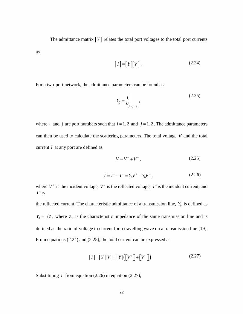
Figure 3.1: HFSS-IE simulation model. A 22pF capacitor in series with
a 1V AC source was connected across the transmitter
terminals. Similarly, a 22pF capacitor was connected across
the receiver terminals. The cables connecting the spirals to
the network analyzer were included in the simulation to
account for the effects they might have in the experimental
results. 26
Figure 3.2: 4NEC2 simulation model. A 22pF capacitor in series with a
1V AC source was connected across the transmitter
terminals. Similarly, a 22pF capacitor was connected across
the receiver terminals. The cables connecting the spirals to
the network analyzer were included in the simulation to
account for the effects they might have in the experimental
results. 26
Figure 3.3(a): Illustration of the experimental setup of the basic model. The
transmitter and the receiver were made with copper wire of
radius 0.814mmr wound in clockwise direction. A 22pF
capacitor in series with a 1V AC source was connected
across the transmitter terminals. Similarly, a 22pF capacitor
viii
was connected across the receiver terminals. Styrofoam
sheets of 2cm thickness were used as substrates. The
transmitter was mounted on a 35cm tall styrofoam box. The
receiver was mounted on a styrofoam box as well and this
box was placed on the transmitter such that the receiver was
perfectly aligned with the transmitter. 27
Figure 3.3(b): Experimental setup of the basic model with the receiver at
32cmd in location 1. The transmitter and the receiver
were made with copper wire of radius 0.814mmr wound
in clockwise direction. A 22pF capacitor in series with a 1V
AC source was connected across the transmitter terminals.
Similarly, a 22pF capacitor was connected across the
receiver terminals. Styrofoam sheets of 2cm thickness were
used as substrates. The transmitter was mounted on a 35cm
tall styrofoam box. The receiver was mounted on a
styrofoam box as well and this box was placed on the
transmitter such that the receiver was perfectly aligned with
the transmitter. 28
Figure 3.3(c): Experimental setup of the basic model with the receiver at
32cmd in location 2. The transmitter and the receiver
were made with copper wire of radius 0.814mmr wound
in clockwise direction. A 22pF capacitor in series with a 1V
AC source was connected across the transmitter terminals.
Similarly, a 22pF capacitor was connected across the
receiver terminals. Styrofoam sheets of 2cm thickness were
used as substrates. The transmitter was mounted on a 35cm
tall styrofoam box. The receiver was mounted on a
styrofoam box as well and this box was placed on the
transmitter such that the receiver was perfectly aligned with
the transmitter. 29
Figure 3.4: Illustration of the top-view of the experimental setup shown
in Figure 3.3. The transmitter and the receiver were made of
copper wire of radius 0.814mmr wound in clockwise
direction. A 22pF capacitor in series with a 1V AC source
was connected across the transmitter terminals. Similarly, a
22pF capacitor was connected across the receiver terminals.
Styrofoam sheets of 2cm thickness were used as substrates.
The transmitter was mounted on a 35cm tall styrofoam box.
The receiver was mounted on a styrofoam box as well and
this box was placed on the transmitter such that the receiver
was directly over the transmitter. 29
ix
Figure 3.5: Illustration of a clockwise wound spiral and a
counterclockwise wound spiral obtained by flipping the
former. The spiral was built on 2cm thick styrofoam sheet. 31
Figure 3.6: Illustration of the experimental setup of the basic model with
the receiver misaligned. The transmitter and the receiver
were made of copper wire of radius 0.814mmr wound in
clockwise direction. A 22pF capacitor in series with a 1V AC
source was connected across the transmitter terminals.
Similarly, a 22pF capacitor was connected across the
receiver terminals. Styrofoam sheets of 2cm thickness were
used as substrates. The transmitter was mounted on a 35cm
tall styrofoam box. The receiver was mounted on a
styrofoam box as well and this box was placed on the
transmitter such that the receiver was misaligned 10cm in
both the x- and y- directions, simultaneously. 32
Figure 3.7: Illustration of the top-view of the experimental setup shown
in Figure 3.6 without the network analyzer. The transmitter
and the receiver were made of copper wire of radius
0.814mmr wound in clockwise direction. A 22pF
capacitor in series with a 1V AC source was connected
across the transmitter terminals. Similarly, a 22pF capacitor
was connected across the receiver terminals. Styrofoam
sheets of 2cm thickness were used as substrates. The
transmitter was mounted on a 35cm tall styrofoam box. The
receiver was mounted on a styrofoam box as well and this
box was placed on the transmitter such that the receiver was
misaligned 10cm in both the x- and y- directions,
simultaneously. 32
Figure 3.8(a): Illustration of the experimental setup of the basic model
using cardboard substrates. The transmitter and the receiver
were made of copper wire of radius 0.814mmr wound in
clockwise direction. A 22pF capacitor in series with a 1V AC
source was connected across the transmitter terminals.
Similarly, a 22pF capacitor was connected across the
receiver terminals. Cardboard sheets of 3mm thickness were
used as substrates. The transmitter was mounted on a 35cm
tall styrofoam box. The receiver was mounted on a
styrofoam box as well and this box was placed on the
transmitter such that the receiver was perfectly aligned with
the transmitter. A 2cm thick styrofoam sheet was inserted
under the cardboard holding the receiver to ensure that the
x
separation distance d was the same for the experiments with
styrofoam and cardboard substrates. The thickness of the
cardboard substrate was assumed to be negligible to simplify
the experiment. 34
Figure 3.8(b): Experimental setup of the basic model using cardboard
substrate. The transmitter and the receiver were made of
copper wire of radius 0.814mmr wound in clockwise
direction. A 22pF capacitor in series with a 1V AC source
was connected across the transmitter terminals. Similarly, a
22pF capacitor was connected across the receiver terminals.
Cardboard sheets of 3mm thickness were used as substrates.
The transmitter was mounted on a 35cm tall styrofoam box.
The receiver was mounted on a styrofoam box as well and
this box was placed on the transmitter such that the receiver
was perfectly aligned with the transmitter. A 2cm thick
styrofoam sheet was inserted under the cardboard holding
the receiver to ensure that the separation distance d was the
same for the experiments with styrofoam and cardboard
substrates. The thickness of the cardboard substrate was
assumed to be negligible to simplify the experiment. 35
Figure 3.9: Illustration of the top-view of the experimental setup of the
array model without the network analyzer. A 2 x 2 array was
formed by the transmitter and the three parasites. Each spiral
was made of copper wire of radius 0.814mmr wound in
clockwise direction. The adjacent spirals were placed 2cm
apart. A 22pF capacitor in series with a 1V AC source was
connected across the transmitter terminals. Similarly, a 22pF
capacitor was connected across the terminals of the receiver
and the parasites. 36
Figure 3.10: Illustration of the receiver locations. A 2 x 2 array was
formed by the transmitter and three parasites. Scattering
parameter measurements were taken were taken while the
receiver was placed at locations p1, p2, p3, p4, and p5. The
coordinates of the locations are listed in Table 3.2. 37
Figure 3.11(a): Illustration of the array model with the receiver at the
location p1. A 2 x 2 array was formed by the transmitter and
the three parasites and this array was mounted on 35cm tall
boxes to avoid possible coupling with anything on/under the
ground. The receiver was also mounted on a styrofoam box
xi
and scattering parameter measurements were taken with
receiver centered at locations p1, p2, p3, p4, and p5. 38
Figure 3.11(b): Experimental setup of the array model with the receiver at
the location p1. A 2 x 2 array was formed by the transmitter
and the three parasites and this array was mounted on 35cm
tall boxes to avoid possible coupling with anything on/under
the ground. The receiver was also mounted on a styrofoam
box and scattering parameter measurements were taken with
receiver centered at locations p1, p2, p3, p4, and p5. 38
Figure 4.1: Transmission efficiency versus frequency plot of the basic
model with RxCW at 32cmd in location 1. The
transmitter and the receiver were built on styrofoam
substrates. The peak transmission efficiency was measured
to be 10% at 11.4 MHz. The results obtained from the HFSS-
IE and 4NEC2 simulations agreed pretty well with each
other and they showed a similar trend as the experimental
measurement. However, compared to the simulated results,
the measured resonant frequency was larger and the
measured peak efficiency was smaller. 40
Figure 4.2: Transmission efficiency versus frequency plot of the basic
model with RxCCW at 32cmd in location 1. The
transmitter and the receiver were built on styrofoam
substrates. The peak transmission efficiency was measured
to be 92% at 11.2 MHz. The HFSS-IE and 4NEC2
simulations agreed pretty well with each other and also with
the measurement. 41
Figure 4.3: Transmission efficiency versus frequency plot of the basic
model with RxCW at 14cmd in location 1. The
transmitter and the receiver were built on styrofoam
substrates. The peak transmission efficiency was measured
to be 86% at 11.3 MHz. The HFSS-IE and 4NEC2
simulations agreed pretty well with each other and showed
double humps as would be expected when the transmitter
and the receiver were brought closer. However, the
measurement did not show double humps. 41
Figure 4.4: Transmission efficiency versus frequency plot of the basic
model with RxCCW at 14cmd in location 1. The
transmitter and the receiver were built on styrofoam
substrates. The HFSS-IE and 4NEC2 simulations agreed
xii
pretty well with each other and also with the measurement.
Double humps, as would be expected when the transmitter
and the receiver were brought closer, were seen. Compared
to the simulated results, the measured double humps were
farther apart. The transmission efficiency was measured to
be 96% at 10.14 MHz and 93% at 12.5 MHz. 42
Figure 4.5: Transmission efficiency versus frequency plot of the basic
model with RxCW at 8cmd in location 1. The transmitter
and the receiver were built on styrofoam substrates. The
HFSS-IE and 4NEC2 simulations agreed pretty well with
each other and showed double humps as would be expected
when the transmitter and the receiver were brought closer.
The measurement showed that the double humps were
beginning to appear. The measured transmission efficiency
was 90% or higher for the frequency range of 10.5 MHz to
12.1 MHz. 42
Figure 4.6: Transmission efficiency versus frequency plot of the basic
model with RxCCW at 8cmd in location 1. The
transmitter and the receiver were built on styrofoam
substrates. The HFSS-IE and 4NEC2 simulations agreed
pretty well with each other and also with the measurement.
Double humps, as would be expected when the transmitter
and the receiver were brought closer, were seen. Compared
to the simulated results, the measured double humps were
farther apart. The transmission efficiency was measured to
be 97% at 9.5 MHz and 93% at 13.5 MHz. 43
Figure 4.7: Ideal transmission efficiency versus frequency plot of the
basic model at 32cmd . The capacitors were assigned the
theoretical capacitance values. The coaxial cables that
connected the transmitter and the receiver to the network
analyzer were not included in the simulation. The peak
transmission efficiency was measured to be greater than 90%
at the resonant frequency of 12.4 MHz. The simulation
results for RxCW and RxCCW were exactly the same. Also,
HFSS-IE and 4NEC2 agreed very well with other. 44
Figure 4.8: Ideal transmission efficiency versus frequency plot of the
basic model at 14cmd . The capacitors were assigned the
theoretical capacitance values. The coaxial cables that
connected the transmitter and the receiver to the network
analyzer were not included in the simulation. Double humps,
xiii
as would be expected when the transmitter and the receiver
were brought closer, were seen. The transmission efficiency
was measured to be 93% or higher at 11.5 MHz and 13.6
MHz. The simulation results for RxCW and RxCCW were
exactly the same. Also, HFSS-IE and 4NEC2 agreed very
well with other.
44
Figure 4.9:
Ideal transmission efficiency versus frequency plot of the
basic model at 8cmd . The capacitors were assigned the
theoretical capacitance values. The coaxial cables that
connected the transmitter and the receiver to the network
analyzer were not included in the simulation. Double humps,
as would be expected when the transmitter and the receiver
were brought closer, were seen. The transmission efficiency
was measured to be 93% or higher at 11 MHz and 13.5 MHz.
The simulation results for RxCW and RxCCW were exactly
the same. Also, HFSS-IE and 4NEC2 agreed very well with
other.
45
Figure 4.10:
Transmission efficiency versus frequency plot of the basic
model in location 1 and location 2 when 32cmd . The
transmitter and the receiver were built on styrofoam
substrates. The scattering parameter measurements taken in
location 1 and location 2 were almost identical confirming
that the environment of the experimental setup has negligible
effect on the measurements.
46
Figure 4.11:
Transmission efficiency versus frequency plot of the basic
model in location 1 and location 2 when 14cmd . The
transmitter and the receiver were built on styrofoam
substrates. The scattering parameter measurements taken in
location 1 and location 2 were almost identical confirming
that the environment of the experimental setup has negligible
effect on the measurements. 46
Figure 4.12:
Transmission efficiency versus frequency plot of the basic
model in location 1 and location 2 when 8cmd . The
transmitter and the receiver were built on styrofoam
substrates. The scattering parameter measurements taken in
location 1 and location 2 were almost identical confirming
that the environment of the experimental setup has negligible
effect on the measurements.
47
xiv
Figure 4.13: Transmission efficiency versus frequency plot of the basic
model in location 1 with styrofoam and cardboard substrates
when 32cmd . The spiral on the styrofoam sheet was built
with multiple pieces of wires soldered at the corners whereas
the spiral on the cardboard sheet was built with one piece of
wire bent at the corners. The scattering parameter
measurements of the basic model with the cardboard
substrate compared to those with the styrofoam substrate was
very similar confirming the reproducibility of the
experiment. 48
Figure 4.14: Transmission efficiency versus frequency plot of the basic
model in location 1 with styrofoam and cardboard substrates
when 14cmd . The spiral on the styrofoam sheet was built
with multiple pieces of wires soldered at the corners whereas
the spiral on the cardboard sheet was built with one piece of
wire bent at the corners. The scattering parameter
measurements of the basic model with the cardboard
substrate compared to those with the styrofoam substrate was
very similar confirming the reproducibility of the
experiment. 48
Figure 4.15: Transmission efficiency versus frequency plot of the basic
model in location 1 with styrofoam and cardboard substrates
when 8cmd . The spiral on the styrofoam sheet was built
with multiple pieces of wires soldered at the corners whereas
the spiral on the cardboard sheet was built with one piece of
wire bent at the corners. The scattering parameter
measurements of the basic model with the cardboard
substrate compared to those with the styrofoam substrate was
very similar confirming the reproducibility of the
experiment. 49
Figure 4.16: Transmission efficiency versus frequency plot of the basic
model in location 1 with the receiver perfectly aligned and
misaligned when 32cmd . The transmitter and the
receiver were built on styrofoam substrates. The peak
transmission efficiency dropped from 10% to 3% for RxCW,
and from 92% to 85% for RxCCW when the receiver was
misaligned 10cm in both the x- and y- directions
simultaneously. The resonant frequency was approximately
the same. 50
xv
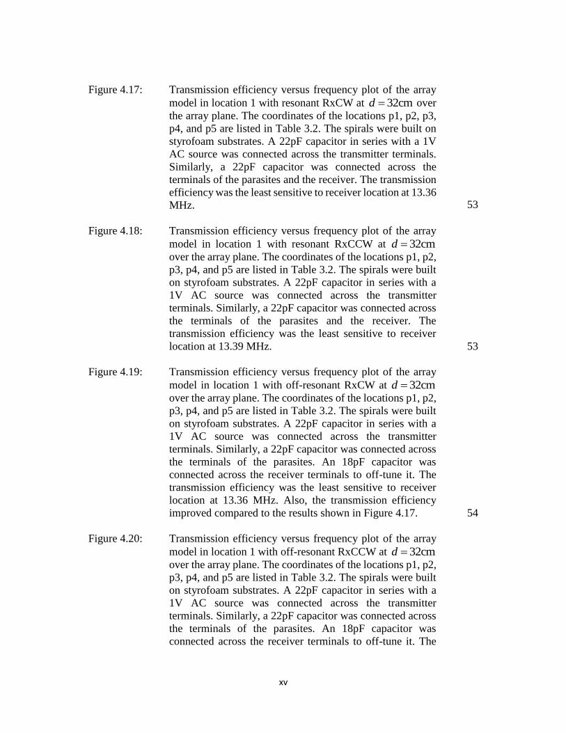
Figure 4.17: Transmission efficiency versus frequency plot of the array
model in location 1 with resonant RxCW at 32cmd over
the array plane. The coordinates of the locations p1, p2, p3,
p4, and p5 are listed in Table 3.2. The spirals were built on
styrofoam substrates. A 22pF capacitor in series with a 1V
AC source was connected across the transmitter terminals.
Similarly, a 22pF capacitor was connected across the
terminals of the parasites and the receiver. The transmission
efficiency was the least sensitive to receiver location at 13.36
MHz. 53
Figure 4.18: Transmission efficiency versus frequency plot of the array
model in location 1 with resonant RxCCW at 32cmd
over the array plane. The coordinates of the locations p1, p2,
p3, p4, and p5 are listed in Table 3.2. The spirals were built
on styrofoam substrates. A 22pF capacitor in series with a
1V AC source was connected across the transmitter
terminals. Similarly, a 22pF capacitor was connected across
the terminals of the parasites and the receiver. The
transmission efficiency was the least sensitive to receiver
location at 13.39 MHz. 53
Figure 4.19: Transmission efficiency versus frequency plot of the array
model in location 1 with off-resonant RxCW at 32cmd
over the array plane. The coordinates of the locations p1, p2,
p3, p4, and p5 are listed in Table 3.2. The spirals were built
on styrofoam substrates. A 22pF capacitor in series with a
1V AC source was connected across the transmitter
terminals. Similarly, a 22pF capacitor was connected across
the terminals of the parasites. An 18pF capacitor was
connected across the receiver terminals to off-tune it. The
transmission efficiency was the least sensitive to receiver
location at 13.36 MHz. Also, the transmission efficiency
improved compared to the results shown in Figure 4.17. 54
Figure 4.20: Transmission efficiency versus frequency plot of the array
model in location 1 with off-resonant RxCCW at 32cmd
over the array plane. The coordinates of the locations p1, p2,
p3, p4, and p5 are listed in Table 3.2. The spirals were built
on styrofoam substrates. A 22pF capacitor in series with a
1V AC source was connected across the transmitter
terminals. Similarly, a 22pF capacitor was connected across
the terminals of the parasites. An 18pF capacitor was
connected across the receiver terminals to off-tune it. The
xvi
transmission efficiency was the least sensitive to receiver
location at 13.39 MHz. Also, the transmission efficiency
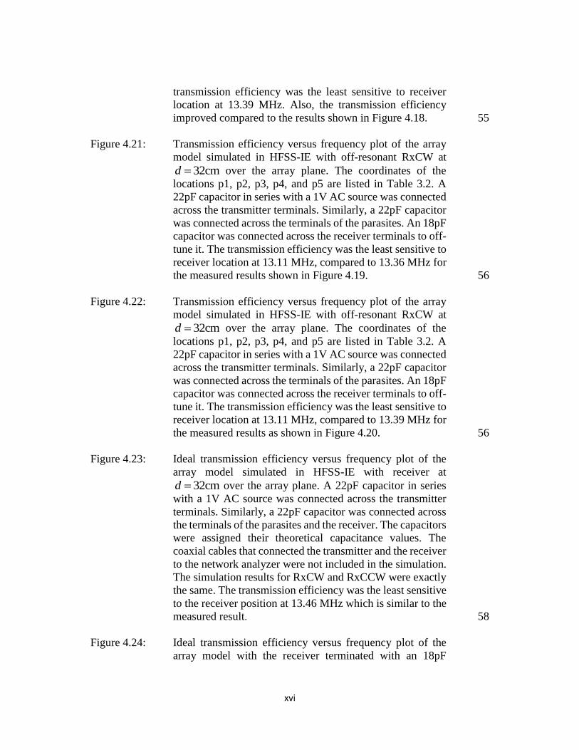
improved compared to the results shown in Figure 4.18. 55
Figure 4.21: Transmission efficiency versus frequency plot of the array
model simulated in HFSS-IE with off-resonant RxCW at
32cmd over the array plane. The coordinates of the
locations p1, p2, p3, p4, and p5 are listed in Table 3.2. A
22pF capacitor in series with a 1V AC source was connected
across the transmitter terminals. Similarly, a 22pF capacitor
was connected across the terminals of the parasites. An 18pF
capacitor was connected across the receiver terminals to off-
tune it. The transmission efficiency was the least sensitive to
receiver location at 13.11 MHz, compared to 13.36 MHz for
the measured results shown in Figure 4.19. 56
Figure 4.22: Transmission efficiency versus frequency plot of the array
model simulated in HFSS-IE with off-resonant RxCW at
32cmd over the array plane. The coordinates of the
locations p1, p2, p3, p4, and p5 are listed in Table 3.2. A
22pF capacitor in series with a 1V AC source was connected
across the transmitter terminals. Similarly, a 22pF capacitor
was connected across the terminals of the parasites. An 18pF
capacitor was connected across the receiver terminals to off-
tune it. The transmission efficiency was the least sensitive to
receiver location at 13.11 MHz, compared to 13.39 MHz for
the measured results as shown in Figure 4.20. 56
Figure 4.23: Ideal transmission efficiency versus frequency plot of the
array model simulated in HFSS-IE with receiver at
32cmd over the array plane. A 22pF capacitor in series
with a 1V AC source was connected across the transmitter
terminals. Similarly, a 22pF capacitor was connected across
the terminals of the parasites and the receiver. The capacitors
were assigned their theoretical capacitance values. The
coaxial cables that connected the transmitter and the receiver
to the network analyzer were not included in the simulation.
The simulation results for RxCW and RxCCW were exactly
the same. The transmission efficiency was the least sensitive
to the receiver position at 13.46 MHz which is similar to the
measured result. 58
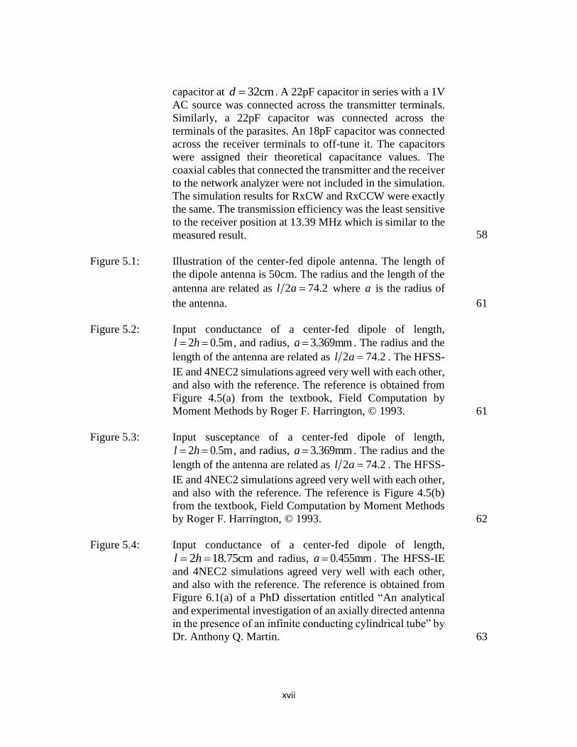
Figure 4.24: Ideal transmission efficiency versus frequency plot of the
array model with the receiver terminated with an 18pF
xvii
capacitor at 32cmd . A 22pF capacitor in series with a 1V
AC source was connected across the transmitter terminals.
Similarly, a 22pF capacitor was connected across the
terminals of the parasites. An 18pF capacitor was connected
across the receiver terminals to off-tune it. The capacitors
were assigned their theoretical capacitance values. The
coaxial cables that connected the transmitter and the receiver
to the network analyzer were not included in the simulation.
The simulation results for RxCW and RxCCW were exactly
the same. The transmission efficiency was the least sensitive
to the receiver position at 13.39 MHz which is similar to the
measured result. 58
Figure 5.1: Illustration of the center-fed dipole antenna. The length of
the dipole antenna is 50cm. The radius and the length of the
antenna are related as 2 74.2l a where a is the radius of
the antenna. 61
Figure 5.2: Input conductance of a center-fed dipole of length,
2 0.5ml h , and radius, 3.369mma . The radius and the
length of the antenna are related as 2 74.2l a . The HFSS-
IE and 4NEC2 simulations agreed very well with each other,
and also with the reference. The reference is obtained from
Figure 4.5(a) from the textbook, Field Computation by
Moment Methods by Roger F. Harrington, © 1993. 61
Figure 5.3: Input susceptance of a center-fed dipole of length,
2 0.5ml h , and radius, 3.369mma . The radius and the
length of the antenna are related as 2 74.2l a . The HFSS-
IE and 4NEC2 simulations agreed very well with each other,
and also with the reference. The reference is Figure 4.5(b)
from the textbook, Field Computation by Moment Methods
by Roger F. Harrington, © 1993. 62
Figure 5.4: Input conductance of a center-fed dipole of length,
2 18.75cml h and radius, 0.455mma . The HFSS-IE
and 4NEC2 simulations agreed very well with each other,
and also with the reference. The reference is obtained from
Figure 6.1(a) of a PhD dissertation entitled “An analytical
and experimental investigation of an axially directed antenna
in the presence of an infinite conducting cylindrical tube” by
Dr. Anthony Q. Martin. 63
xviii
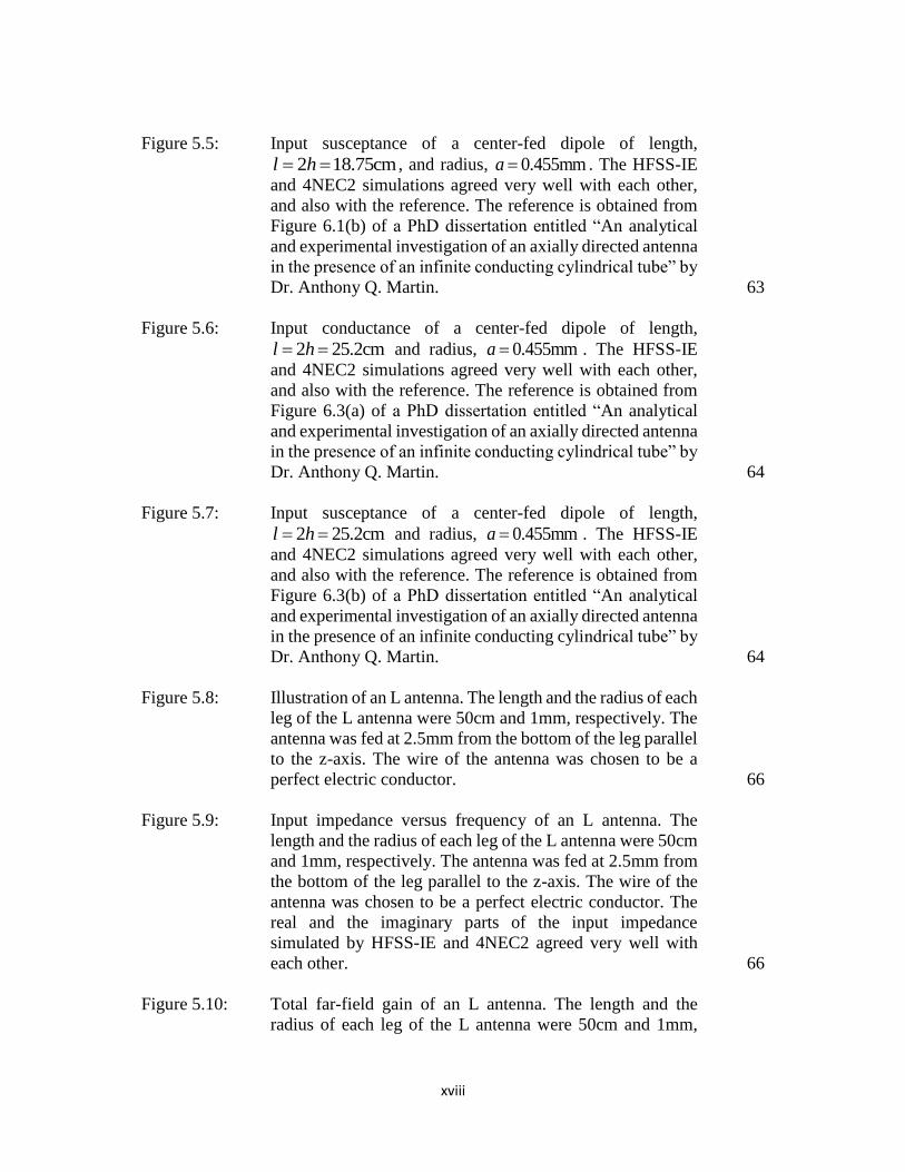
Figure 5.5: Input susceptance of a center-fed dipole of length,
2 18.75cml h , and radius, 0.455mma . The HFSS-IE
and 4NEC2 simulations agreed very well with each other,
and also with the reference. The reference is obtained from
Figure 6.1(b) of a PhD dissertation entitled “An analytical
and experimental investigation of an axially directed antenna
in the presence of an infinite conducting cylindrical tube” by
Dr. Anthony Q. Martin. 63
Figure 5.6: Input conductance of a center-fed dipole of length,
2 25.2cml h and radius, 0.455mma . The HFSS-IE
and 4NEC2 simulations agreed very well with each other,
and also with the reference. The reference is obtained from
Figure 6.3(a) of a PhD dissertation entitled “An analytical
and experimental investigation of an axially directed antenna
in the presence of an infinite conducting cylindrical tube” by
Dr. Anthony Q. Martin. 64
Figure 5.7: Input susceptance of a center-fed dipole of length,
2 25.2cml h and radius, 0.455mma . The HFSS-IE
and 4NEC2 simulations agreed very well with each other,
and also with the reference. The reference is obtained from
Figure 6.3(b) of a PhD dissertation entitled “An analytical
and experimental investigation of an axially directed antenna
in the presence of an infinite conducting cylindrical tube” by
Dr. Anthony Q. Martin. 64
Figure 5.8: Illustration of an L antenna. The length and the radius of each
leg of the L antenna were 50cm and 1mm, respectively. The
antenna was fed at 2.5mm from the bottom of the leg parallel
to the z-axis. The wire of the antenna was chosen to be a
perfect electric conductor. 66
Figure 5.9: Input impedance versus frequency of an L antenna. The
length and the radius of each leg of the L antenna were 50cm
and 1mm, respectively. The antenna was fed at 2.5mm from
the bottom of the leg parallel to the z-axis. The wire of the
antenna was chosen to be a perfect electric conductor. The
real and the imaginary parts of the input impedance
simulated by HFSS-IE and 4NEC2 agreed very well with
each other. 66
Figure 5.10: Total far-field gain of an L antenna. The length and the
radius of each leg of the L antenna were 50cm and 1mm,
xix
respectively. The antenna was fed at 2.5mm from the bottom
of the leg parallel to z-axis. The wire of the antenna was
chosen to be a perfect electric conductor. The total far-field
gain simulated by HFSS-IE and 4NEC2 agreed very well
with each other. 67
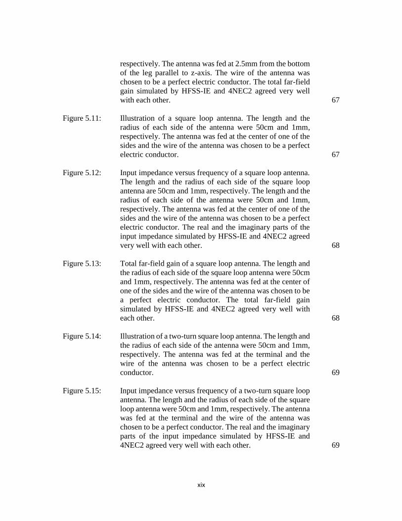
Figure 5.11: Illustration of a square loop antenna. The length and the
radius of each side of the antenna were 50cm and 1mm,
respectively. The antenna was fed at the center of one of the
sides and the wire of the antenna was chosen to be a perfect
electric conductor. 67
Figure 5.12: Input impedance versus frequency of a square loop antenna.
The length and the radius of each side of the square loop
antenna are 50cm and 1mm, respectively. The length and the
radius of each side of the antenna were 50cm and 1mm,
respectively. The antenna was fed at the center of one of the
sides and the wire of the antenna was chosen to be a perfect
electric conductor. The real and the imaginary parts of the
input impedance simulated by HFSS-IE and 4NEC2 agreed
very well with each other. 68
Figure 5.13: Total far-field gain of a square loop antenna. The length and
the radius of each side of the square loop antenna were 50cm
and 1mm, respectively. The antenna was fed at the center of
one of the sides and the wire of the antenna was chosen to be
a perfect electric conductor. The total far-field gain
simulated by HFSS-IE and 4NEC2 agreed very well with
each other. 68
Figure 5.14: Illustration of a two-turn square loop antenna. The length and
the radius of each side of the antenna were 50cm and 1mm,
respectively. The antenna was fed at the terminal and the
wire of the antenna was chosen to be a perfect electric
conductor. 69
Figure 5.15: Input impedance versus frequency of a two-turn square loop
antenna. The length and the radius of each side of the square
loop antenna were 50cm and 1mm, respectively. The antenna
was fed at the terminal and the wire of the antenna was
chosen to be a perfect conductor. The real and the imaginary
parts of the input impedance simulated by HFSS-IE and
4NEC2 agreed very well with each other. 69
xx
Figure 5.16: Total far-field gain of a two-turn square loop antenna. The
length and the radius of each side of the square loop antenna
were 50cm and 1mm, respectively. The antenna was fed at
the terminal and the wire of the antenna was chosen to be a
perfect conductor. The total far-field gain simulated by
HFSS-IE and 4NEC2 agreed very well with each other. 70
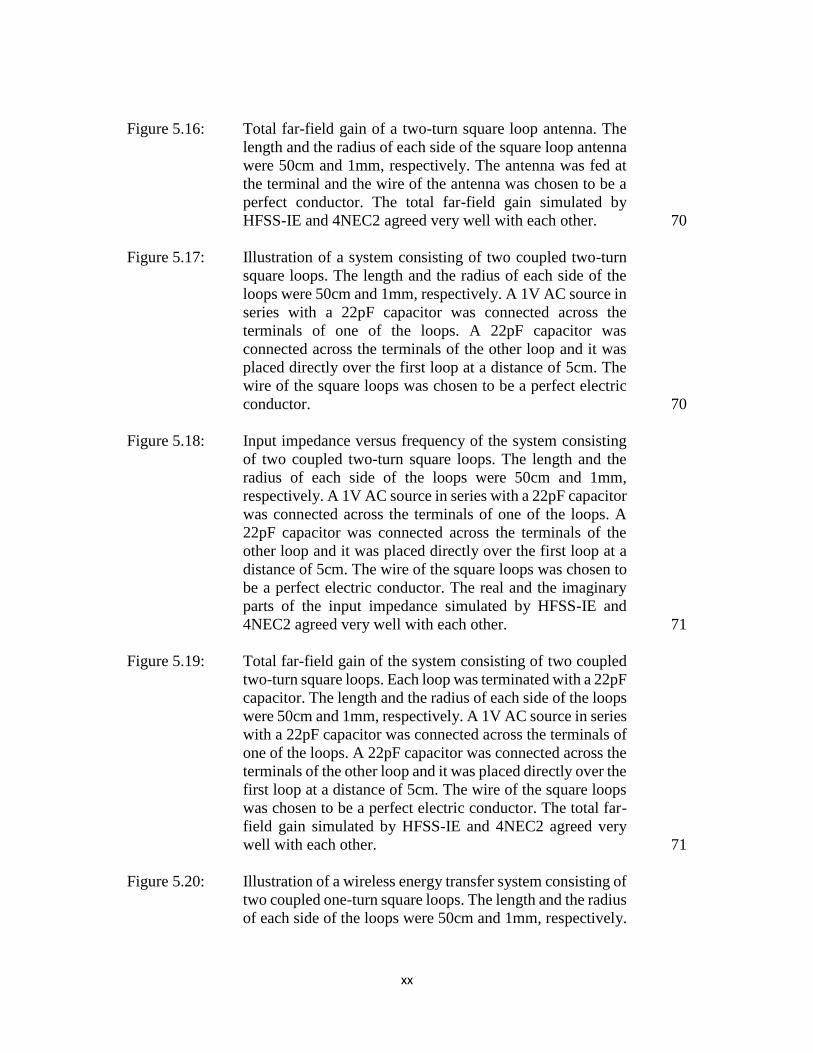
Figure 5.17: Illustration of a system consisting of two coupled two-turn
square loops. The length and the radius of each side of the
loops were 50cm and 1mm, respectively. A 1V AC source in
series with a 22pF capacitor was connected across the
terminals of one of the loops. A 22pF capacitor was
connected across the terminals of the other loop and it was
placed directly over the first loop at a distance of 5cm. The
wire of the square loops was chosen to be a perfect electric
conductor. 70
Figure 5.18: Input impedance versus frequency of the system consisting
of two coupled two-turn square loops. The length and the
radius of each side of the loops were 50cm and 1mm,
respectively. A 1V AC source in series with a 22pF capacitor
was connected across the terminals of one of the loops. A
22pF capacitor was connected across the terminals of the
other loop and it was placed directly over the first loop at a
distance of 5cm. The wire of the square loops was chosen to
be a perfect electric conductor. The real and the imaginary
parts of the input impedance simulated by HFSS-IE and
4NEC2 agreed very well with each other. 71
Figure 5.19: Total far-field gain of the system consisting of two coupled
two-turn square loops. Each loop was terminated with a 22pF
capacitor. The length and the radius of each side of the loops
were 50cm and 1mm, respectively. A 1V AC source in series
with a 22pF capacitor was connected across the terminals of
one of the loops. A 22pF capacitor was connected across the
terminals of the other loop and it was placed directly over the
first loop at a distance of 5cm. The wire of the square loops
was chosen to be a perfect electric conductor. The total far-
field gain simulated by HFSS-IE and 4NEC2 agreed very
well with each other. 71
Figure 5.20: Illustration of a wireless energy transfer system consisting of
two coupled one-turn square loops. The length and the radius
of each side of the loops were 50cm and 1mm, respectively.
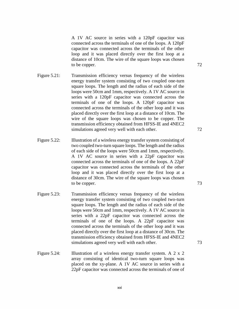
xxi
A 1V AC source in series with a 120pF capacitor was
connected across the terminals of one of the loops. A 120pF
capacitor was connected across the terminals of the other
loop and it was placed directly over the first loop at a
distance of 10cm. The wire of the square loops was chosen
to be copper. 72
Figure 5.21: Transmission efficiency versus frequency of the wireless
energy transfer system consisting of two coupled one-turn
square loops. The length and the radius of each side of the
loops were 50cm and 1mm, respectively. A 1V AC source in
series with a 120pF capacitor was connected across the
terminals of one of the loops. A 120pF capacitor was
connected across the terminals of the other loop and it was
placed directly over the first loop at a distance of 10cm. The
wire of the square loops was chosen to be copper. The
transmission efficiency obtained from HFSS-IE and 4NEC2
simulations agreed very well with each other. 72
Figure 5.22: Illustration of a wireless energy transfer system consisting of
two coupled two-turn square loops. The length and the radius
of each side of the loops were 50cm and 1mm, respectively.
A 1V AC source in series with a 22pF capacitor was
connected across the terminals of one of the loops. A 22pF
capacitor was connected across the terminals of the other
loop and it was placed directly over the first loop at a
distance of 30cm. The wire of the square loops was chosen
to be copper. 73
Figure 5.23: Transmission efficiency versus frequency of the wireless
energy transfer system consisting of two coupled two-turn
square loops. The length and the radius of each side of the
loops were 50cm and 1mm, respectively. A 1V AC source in
series with a 22pF capacitor was connected across the
terminals of one of the loops. A 22pF capacitor was
connected across the terminals of the other loop and it was
placed directly over the first loop at a distance of 30cm. The
transmission efficiency obtained from HFSS-IE and 4NEC2
simulations agreed very well with each other. 73
Figure 5.24: Illustration of a wireless energy transfer system. A 2 x 2
array consisting of identical two-turn square loops was
placed on the xy-plane. A 1V AC source in series with a
22pF capacitor was connected across the terminals of one of
xxii
the loops. A 22pF capacitor was connected across the
terminals of the rest of the loops. One of these loops was
placed directly over the excited loop at a distance of 30cm.
The length and the radius of each side of the loops were
50cm and 1mm, respectively. The wire of the square loops
was chosen to be copper. 74
Figure 5.25: Transmission efficiency versus frequency of the array model
shown in Figure 5.24. A 2 x 2 array consisting of identical
two-turn square loops was placed on the xy-plane. A 1V AC
source in series with a 22pF capacitor was connected across
the terminals of one of the loops. A 22pF capacitor was
connected across the terminals of the rest of the loops. One
of these loops was placed directly over the excited loop at a
distance of 30cm. The length and the radius of each side of
the loops were 50cm and 1mm, respectively. The wire of the
square loops was chosen to be copper. The transmission
efficiency plot obtained from HFSS-IE and 4NEC2
simulations had similar trend but there was some frequency
shift. 74

xxiii
LIST OF TABLES
Table 3.1: The comparison of the theoretical and measured capacitance. An
impedance analyzer was used to measure the capacitance. 25
Table 3.2: The coordinates of the receiver locations illustrated in Figure 3.10.
The separation distance d was the vertical separation of the
receiver from the transmitter or the array plane. 37

1
CHAPTER 1
INTRODUCTION
In 1914, Nikola Tesla filed a US patent entitled “Apparatus for Transmitting
Electrical Energy” in which he describes his work on transporting electrical energy over
long distances without a carrier medium (e.g. wirelessly) [1]. The famous Tesla coil,
however, involved undesirably large electric fields. Tesla hoped to transmit electrical
energy wirelessly on a global scale. The Wardenclyffe Tower [2] was erected to test Tesla’s
world wireless system. The Wardenclyffe Tower stood 187 feet tall with a spherical top
that was 68 feet in diameter. Due to discontinued funding, Tesla was forced to quit his
Wardenclyffe experiments and his dream of powering the world wirelessly was never
realized [2].
Magnetic induction has been used to wirelessly transfer energy over short distance
for several years now. Induction stoves are common household appliances utilizing
magnetic induction. Recently, wireless charging of portable electronic devices like cell
phones and tablets has gained popularity. Qi is the leading wireless charging standard for
electronics and is in hundreds of consumer products [3]. The wireless electric toothbrush
is another common household item utilizing magnetic induction. Wireless charging of
electric vehicles is a popular research topic and companies like Witricity, Momentum
Dynamics, and Plugless in the US are working on the commercialization. Although

2
wireless energy transfer by magnetic induction has seen commercial success through
induction stoves, wireless electric toothbrushes, and Qi charging, wireless charging of
electric vehicles is just starting to receive interest.
In short-range magnetic induction, the energy transfer distance ( TRANSL ) is much
less than the device dimension ( DEVL ), i.e., TRANS DEVL L . This ensures strong coupling
between the transmitter and receiver coils. Coupling refers to the transfer of energy from
one circuit to another. Electromagnetic energy can couple from a source to a receptor in
one of the four ways: conducted (electrical current), inductively coupled (magnetic field),
capacitively coupled (electrical field), and radiated (electromagnetic field) [4]. In electric
vehicle charging applications, magnetic coupling is utilized to couple energy from the
transmitter to the receiver. The transmitter and the receiver are electrically small, i.e.,
DEVL , where is the wavelength of the AC source fed at the transmitter terminals.
The receiver is placed in the reactive near-field region of the transmitter. For an electrically
small circular loop of a thin wire, the magnetic field decays as 31 r in the near-field region
where r is the radial distance from the loop center. Near-field for an electrically small
circular loop is defined as 2r [20]. In transformers, ferromagnetic cores are used
to contain the magnetic field [17]. However, in electric vehicle applications, the transmitter
and the receiver coils are separated by an air gap and the transfer distance is similar to the
device dimension, i.e., TRANS DEVL L . Since the magnetic field decays as 31 r , the
coupling between the transmitter and receiver gets much weaker as the transfer distance

3
gets larger [25]. The absence of a ferromagnetic core also contributes to weak coupling. In
2007, a research team at the Massachusetts Institute of Technology (MIT) successfully
demonstrated medium-range wireless energy transfer using resonant magnetic coupling
[5]. Medium-range implies that the transfer distance is up to a few times larger than the
device dimension. Two resonant objects tend to exchange energy efficiently. Hence, by
operating the coils at a resonant frequency, high-transmission efficiency can be achieved
even when the coupling is weak [5]. The research work for this thesis was inspired, in part,
by the resonant magnetic induction for medium-range wireless energy transfer for electric
vehicle charging.
HFSS-IE and 4NEC2 are the simulation tools used in the research. HFSS-IE is a
part of the Ansys electromagnetics package which is a commercial software and costs
thousands of dollars. HFSS-IE is an integral equation solver that uses the method of
moments technique to solve for the currents on the surfaces of conducting and dielectric
objects in open region. HFSS-IE is spin-off of HFSS. HFSS was originally developed by
Zoltan Cendes and his colleagues at the Carnegie Mellon University in the 1980s. Further
development of HFSS resulted in the formation of the company, Ansoft, which was later
acquired by Ansys [29]. NEC-2 (Numerical Electromagnetics code) is a software used for
finding the electromagnetic response of an arbitrary structure consisting of wires and
surfaces. The structure can be located in free space or over a ground plane. The analysis is
done using the numerical solution of integral equations for induced currents. NEC was
developed at the Lawrence Livermore Laboratory, Livermore, California under the

4
sponsorship of the Naval Ocean Systems Center and the Air Force Weapons Laboratory.
4NEC2 was developed by Arie Voors after NEC-2 Fortran code was made public by the
Lawrence Livermore Laboratory. 4NEC2 provides an easy-to-use interface for creating
models, running simulations, and displaying simulation results in a graphical format. Also,
4NEC2 is available for free [7].
Another important aspect of the research is HFSS-IE and 4NEC2 validation. This
was done by simulating wire antennas and comparing the results with those obtained from
a textbook and a PhD dissertation. Other structures like square loops and systems of
coupled loops were also simulated and the HFSS-IE and 4NEC2 simulation results were
compared against each other. The goal was to check the rigidity of 4NEC2 compared to
HFSS-IE.
5
CHAPTER 2
I. BACKGROUND
Electromagnetism was discovered by a Danish scientist, Hans Christian Oersted, in
1820 [8][9]. He observed a temporary deflection of a compass needle sitting nearby a
current-carrying wire. This happened at the moment the DC current from a battery was
switched on or off; this showed that a change in electric current in a wire produced a
temporary magnetic effect in its vicinity [8]. Oersted’s discovery is true for DC current
only. Around the same time, French physicist and mathematician André-Marie Ampère
showed that two current-carrying wires placed parallel and close to each other generated
magnetic lines of force that caused the wires to attract or repel each other depending on
whether the currents were flowing in the same or opposite directions [8][10]. The works of
Oersted and Ampère confirmed that electricity could be converted into magnetism. It took
another few years to do the reverse: to produce electricity from magnetism [8][12].
Faraday’s research mostly focused on the interaction between the electric current,
magnetic field, and mechanical motion [8][12]. In 1831, Faraday discovered that a time-
varying magnetic field would produce an electric current [13][18]. This discovery was
published in a paper entitled “Experimental Researches in Electricity” in 1832 [12]. In one
of his experiments, Faraday attempted to induce a current in a coil of wire by switching on
and off the current in another wire. The coils were wound on the opposite sides of an un-

6
magnetized iron ring. One of the coils was connected to a battery and the other to a
galvanometer. He observed deflections on the galvanometer every time the battery was
switched on and off [8][12]. Faraday successfully demonstrated the induction of current
from magnetism and, in doing so, he had invented the first electrical transformer. American
scientist, Joseph Henry also produced electricity from magnetism, independently from
Faraday [14][15]. But Faraday published first and hence gets the credit for the discovery
[15]. Faraday’s discoveries laid the foundation for electric machines like generators and
motors. It is impossible to imagine today’s world without electricity. Faraday’s discovery
is what made possible the generation of AC electricity using generators, power
transmission using transformers, and motors running the industries [16]. Faraday’s work is
of particular importance to us while talking about wireless energy transfer which is one of
the main topics of this thesis.
As stated before, the simplest magnetic induction charging system consists of two
coils: a transmitter coil and a receiver. The electric transformer that Faraday built as part
of his experiment on induction is basically what is used in wireless energy transfer. The
only difference is that instead of the iron ring, or a magnetic core, an air core is used in
wireless energy transfer. The coils that Faraday used were helices. Similarly, conventional
transformers use helical coils. However, for wireless energy transfer, coils of any shape
(e.g. circular, rectangular, etc.) can be used. In fact, spirals and loops can be used as well.

7
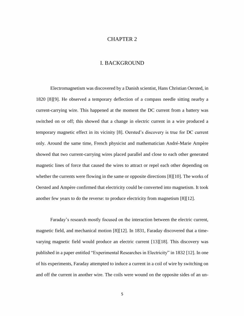
Shown in Figure 2.1 are two conducting circular loops, transmitter and receiver,
respectively. The AC power source connected to the transmitter causes a time varying
electric current to flow in it. This time varying electric current creates a time-varying
magnetic field H . This magnetic field can be determined by using the Ampere’s circuit
law which states that the line integral of H around a closed path is the same as the net
current encI enclosed by the path [13][17]. Ampere’s circuit law can be expressed as
enc
c
d I H l , (2.1)
where dl is the differential element of the conducting loop in the direction of the current.
The magnetic field H is related to the magnetic flux density B as
0B H , (2.2)
where 0 is a constant known as the permeability of free space. The constant has the value
of
74 10
H/m. (2.3)
The direction of the magnetic field generated by the electric current is determined using
the right-hand rule with the right-thumb pointing in the direction of the current and the
right-hand fingers encircling the wire in the direction of the magnetic field [13][17].
Faraday discovered that a time-varying magnetic field produces an induced voltage, called
electromotive force (emf) in a closed circuit. [13][17]. If the receiver is placed such that it
crosses the field lines generated by the transmitter current then the time-varying magnetic
field creates a time-varying electric current in the receiver coil. Following his discovery,
Faraday formulated the law which states that the induced emf, emfV (in volts), in any closed

8
circuit is equal to the time rate of change of the magnetic flux linkage by the circuit
[13][17]. Faraday’s law can be expressed as
Total
emf
d dV N
dt dt
,
(2.4)
Where Total N is the total flux linkage, N is the number of turns of the circuit, and
is the flux through each turn. For a circular loop, 1N . The magnetic flux through a
surface S is given by
S
d B S , (2.5)
where the magnetic flux is in Webers (Wb) and the magnetic flux density B is in
Webers per square meter (Wb/m2) or teslas (T). The negative sign in equation (2.4)
indicates that the induced emf opposes the change in the flux producing it. This is known
as Len’z law [13]. Hence, the direction of the induced current in the receiver is such that
the magnetic field induced by it opposes the change in the magnetic flux generated by the
transmitter current. Substituting from equation (2.5) in equation (2.4), the induced emf
can be expressed as
emf
S
dV N d
dt B S .
(2.6)
The induced current indI can then be calculated as
emf
ind
VI
Z ,
(2.7)
where Z is the impedance of the receiver and can be expressed as

9
Z R jX , (2.8)
where R is the resistance and X is the reactance. The reactance results from the
inductance and/or the capacitance of the receiver.
Applications like inductive cooking and portable electronics (cell-phone, tablet,
electric toothbrush, etc.) charging utilize short-range magnetic induction. As discussed
earlier, in short-range magnetic induction, the energy transfer distance ( TRANSL ) is much
less than the device dimension ( DEVL ), i.e., TRANS DEVL L . This ensures strong coupling
between the transmitter and the receiver, and hence the efficiency of energy transfer is
high. However, there are other applications like charging of electric vehicles and medical
implants where it is not always possible to have the transmitter and the receiver sit so close
that tight coupling can be ensured.
10
Figure 2.1: Illustration of how electromagnetic induction works using two conducting circular loops,
transmitter and receiver. The transmitter terminals are connected to an AC voltage source inV which has an
internal impedance of .sZ The magnetic field created by the transmitter current is represented by the field
lines and the arrows represent the direction of the field. When the receiver is placed such that it crosses these
magnetic field lines, current is induced in the receiver. The direction of the current is such that the magnetic
field generated by the induced current opposes the change in the magnetic flux generated by the transmitter
current. The receiver terminals are connected to a load .LoadZ
In electric vehicle charging application, the transmitter can be laid on the ground,
placed on a wall, or mounted on a pole. In this thesis, it is assumed to be on the ground. As
a result, it makes the most sense to place the receiver underneath the electric vehicle. The
energy transfer distance is then approximately the same as the ground clearance of the
electric vehicle. Similarly, for charging medical implants like a pacemaker, the receiver is
placed within the implant so there is a limit as to how close to the receiver the transmitter
11
can be brought. Depending on how far into the body the implant is, it might not be possible
to ensure tight coupling between the coils. However, by operating the weakly coupled coils
at the same resonant frequency, the efficiency of energy transfer can be greatly improved.
II. EQUIVALENT CIRCUIT
The coupled transmitter and receiver can be modeled as an RLC equivalent
circuit. The analysis of this equivalent circuit can be used to show how two loosely coupled
loops of the same resonance exchange energy efficiently at the resonant frequency. In this
section, the circuit model is discussed in detail, the current and voltage equations are
derived, and the results are presented in a graphical format.
The transmitter and the receiver are inductively coupled when the fields produced
by the current in the transmitter links with the receiver and vice versa. The inductively
coupled transmitter and receiver can both be represented by series RLC circuits. The total
resistance, inductance, and capacitance of the transmitter circuit are TR , TL , and TC ,
respectively. Similarly, the total resistance, inductance and capacitance of the receiver
circuit are RR , RL , and RC , respectively. An AC voltage source inV is connected to the
transmitter. The circuit is shown in Figure 2.2. The effect produced by the coupling
between the transmitter and the receiver can be expressed in terms of a property called the
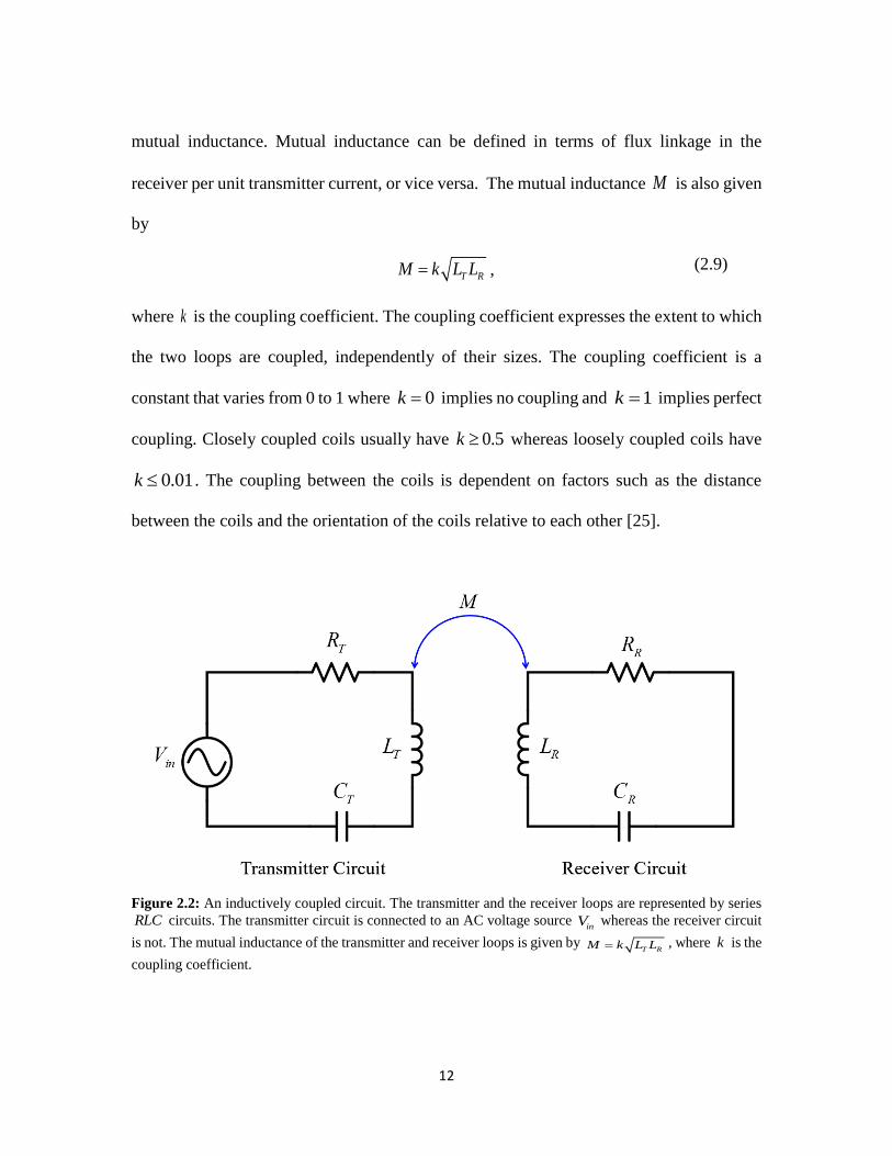
12
mutual inductance. Mutual inductance can be defined in terms of flux linkage in the
receiver per unit transmitter current, or vice versa. The mutual inductance M is also given
by
T RM k L L , (2.9)
where k is the coupling coefficient. The coupling coefficient expresses the extent to which
the two loops are coupled, independently of their sizes. The coupling coefficient is a
constant that varies from 0 to 1 where 0k implies no coupling and 1k implies perfect
coupling. Closely coupled coils usually have 0.5k whereas loosely coupled coils have
0.01k . The coupling between the coils is dependent on factors such as the distance
between the coils and the orientation of the coils relative to each other [25].
Figure 2.2: An inductively coupled circuit. The transmitter and the receiver loops are represented by series
RLC circuits. The transmitter circuit is connected to an AC voltage source inV whereas the receiver circuit
is not. The mutual inductance of the transmitter and receiver loops is given by T RM k L L , where k is the
coupling coefficient.

13
The transmitter self-impedance is given by
2
1 11T T T T T
T T T
Z R j L R j Lj C L C
(2.10)
and the receiver self-impedance is given by
2
1 11R R R R R
R R R
Z R j L R j Lj C L C
,
(2.11)
where 2 f is the angular operating frequency and f is the operating frequency.
Also, the resonant frequencies of the transmitter and the receiver circuits can be written as
1T
T TL C and
1R
R RL C ,
respectively. Similarly, the quality factors, TQ of the transmitter and RQ of the receiver,
can be written as
T
T
T
LQ
R
and
RR
R
LQ
R
.
If the transmitter and the receiver resonate at the same frequency 0 , then
0T R .
A constant can be defined such that
0
.
Hence, the impedance equations in (2.10) and (2.11) can be rewritten as
2
11T T TZ R j L
,
(2.12)
14
2
11R R RZ R j L
.
(2.13)
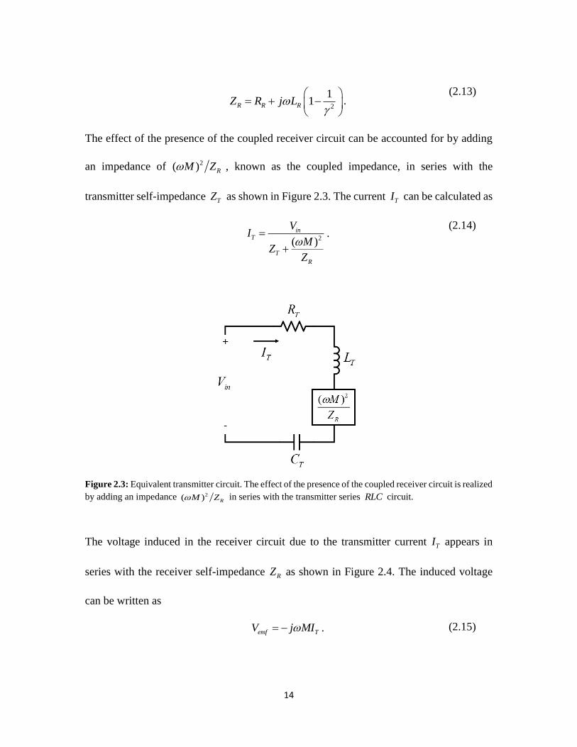
The effect of the presence of the coupled receiver circuit can be accounted for by adding
an impedance of 2( ) RM Z , known as the coupled impedance, in series with the
transmitter self-impedance TZ as shown in Figure 2.3. The current TI can be calculated as
2( )
inT
T
R
VI
MZ
Z
. (2.14)
Figure 2.3: Equivalent transmitter circuit. The effect of the presence of the coupled receiver circuit is realized
by adding an impedance 2( ) RM Z in series with the transmitter series RLC circuit.
The voltage induced in the receiver circuit due to the transmitter current TI appears in
series with the receiver self-impedance RZ as shown in Figure 2.4. The induced voltage
can be written as
emf TV j MI . (2.15)

15
Figure 2.4: Equivalent receiver circuit. The induced emf in the receiver circuit due to the current IT in the
primary circuit is given by emf TV j MI .
The receiver current RI can then be calculated as
emf T
R
R R
V j MII
Z Z
.
(2.16)
Substituting TZ , RZ , and TI from equations (2.12), (2.13) and (2.14) in equation (2.16),
RI can be written as
2
2
0 2 2
1 1 1 1 11 1
inR
T R
T R T R
jkVI
L L k jQ Q Q Q
. (2.17)
The voltage across the capacitor, denoted as oV , can then be calculated as
1o R
R
V Ij C
.
Substituting RI from equation (2.17) and dividing both sides of the equation by inV , the
following can be written
2 2
2
2 2
1
1 1 1 1 11 1
o R
in T
T R T R
V L k
V Lk j
Q Q Q Q
(2.18)
16
where o inV V is known as the transfer function. If the operating frequency is the same
as the resonant frequency 0 then 0 1 . Substituting 1 in equation (2.18), the
transfer function can be written as
2 1
o R
in T
T R
V L k
V Lk
Q Q
.
(2.19)
The transfer function has its maximum value at the critical coupling coefficient ck . This
is obtained by setting 0o
in
Vd
dk V
and showing that
2
20o
in
Vd
dk V
at ck k . The critical
coupling coefficient was obtained to be
1c
T R
kQ Q
. (2.20)
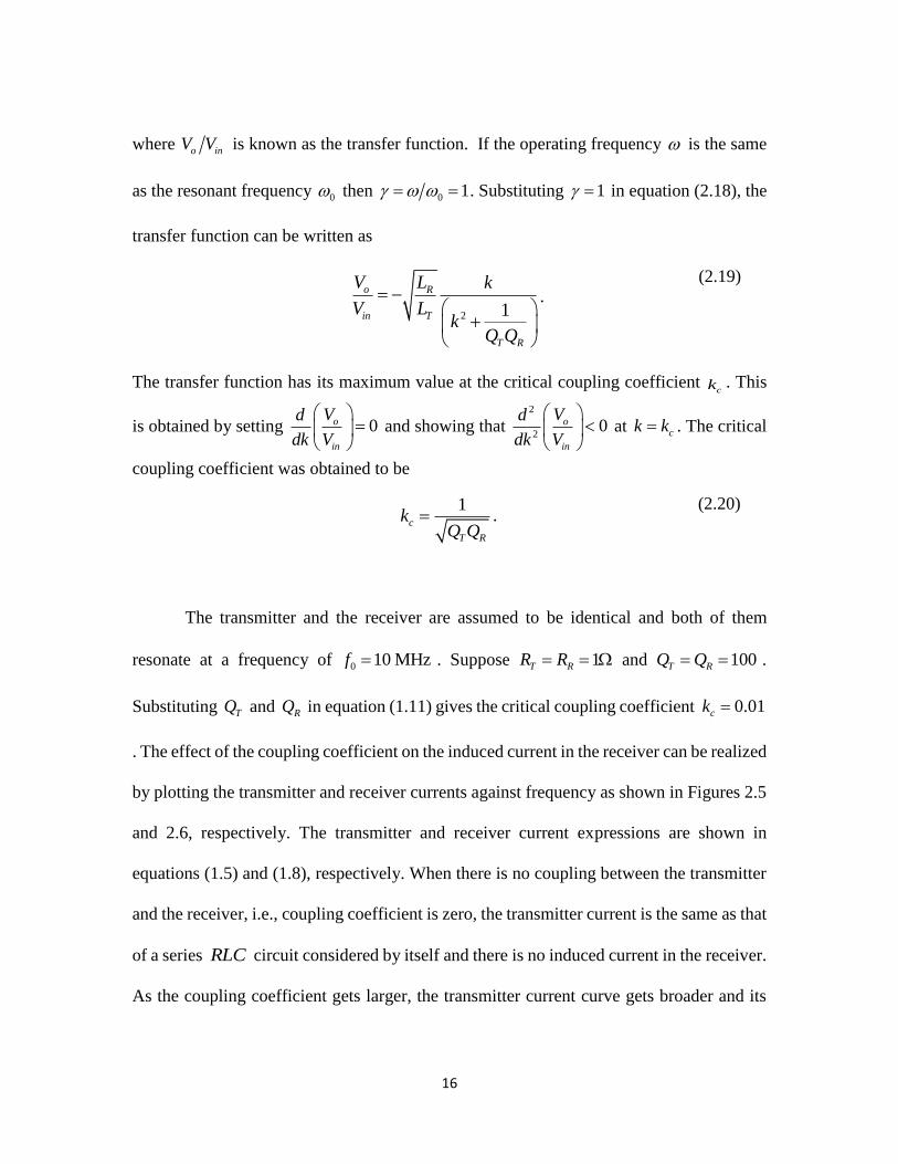
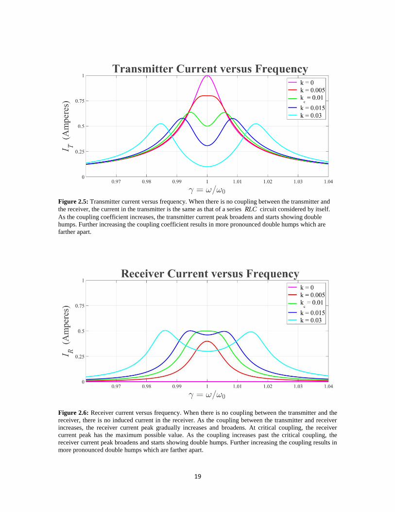
The transmitter and the receiver are assumed to be identical and both of them
resonate at a frequency of 0 10 MHzf . Suppose 1T RR R and 100T RQ Q .
Substituting TQ and RQ in equation (1.11) gives the critical coupling coefficient 0.01ck
. The effect of the coupling coefficient on the induced current in the receiver can be realized
by plotting the transmitter and receiver currents against frequency as shown in Figures 2.5
and 2.6, respectively. The transmitter and receiver current expressions are shown in
equations (1.5) and (1.8), respectively. When there is no coupling between the transmitter
and the receiver, i.e., coupling coefficient is zero, the transmitter current is the same as that
of a series RLC circuit considered by itself and there is no induced current in the receiver.
As the coupling coefficient gets larger, the transmitter current curve gets broader and its

17
peak value gets reduced. At the same time, the receiver current curve also gets broader
whereas its peak value gets larger. As the coupling coefficient approaches its critical value,
the transmitter current curve begins to show double humps. At critical coupling, the
receiver current reaches the maximum possible value. As the coupling increases past the
critical coupling, the double humps in the transmitter current curve become more
pronounced and are farther apart. At the same time, the receiver current begins to show
double humps which become progressively more prominent and get farther apart as the
coupling coefficient increases.
As mentioned earlier, the coupled receiver circuit can be accounted for by adding
an impedance of 2( ) RM Z , known as the coupled impedance, in series with the
transmitter self-impedance. At the resonant frequency, the transmitter self-impedance and
the coupled impedance are both resistive and hence the effective transmitter resistance is
higher than the transmitter self-resistance. As a result, the transmitter current at the resonant
frequency is reduced. Furthermore, as the coupling coefficient is increased, the mutual
coupling increases causing the effective transmitter resistance to increase. So, the larger
the coupling coefficient, the smaller the transmitter current at the resonant frequency. At
frequencies below the resonant frequency, the transmitter self-impedance is capacitive
whereas the coupled impedance is inductive. This inductive coupled impedance neutralizes
the capacitive self-impedance which causes the effective transmitter impedance to get
smaller. The smaller transmitter impedance results in increased transmitter current as a
result of which the transmitter current peak is seen at some frequency below the resonant

18
frequency. Similarly, at frequencies above the resonant frequency, the transmitter self-
impedance is inductive whereas the coupled impedance is capacitive. This capacitive
coupled impedance neutralizes the inductive self-impedance which also causes the
effective transmitter impedance to get smaller. The smaller transmitter impedance results
in increased transmitter current as a result of which the transmitter current peak is also seen
at some frequency above the resonant frequency. The net effect of the coupled impedance
is to lower the transmitter current at the resonant frequency and to increase the transmitter
current at frequencies below and above the resonant frequencies. The magnitude of this
effect increases with increasing coupling coefficient. When the coupling coefficient is
critical or larger, the coupled impedance is the major factor determining the effective
transmitter impedance which in turn determines the transmitter current. The receiver
current is determined by the voltage induced in the receiver by the transmitter current and
the receiver self-impedance. Since emf TV j MI the induced voltage varies with
frequency in almost exactly the same way as the transmitter current TI .
The coupling coefficient is inversely proportional to the separation distance d
between the transmitter and the receiver. Hence, as the loops are brought closer together,
the coupling coefficient increases. The derivation, the discussion, and the plots presented
in this section are important because they provide an explanation to the measurements
obtained for the basic model with the experiment conducted for 8cm,14cm, and 32cm.d
The experimental set up is discussed and illustrated in detail in Chapter 3 and the results
are presented in Chapter 5.
19
Figure 2.5: Transmitter current versus frequency. When there is no coupling between the transmitter and
the receiver, the current in the transmitter is the same as that of a series RLC circuit considered by itself.
As the coupling coefficient increases, the transmitter current peak broadens and starts showing double
humps. Further increasing the coupling coefficient results in more pronounced double humps which are
farther apart.
Figure 2.6: Receiver current versus frequency. When there is no coupling between the transmitter and the
receiver, there is no induced current in the receiver. As the coupling between the transmitter and receiver
increases, the receiver current peak gradually increases and broadens. At critical coupling, the receiver
current peak has the maximum possible value. As the coupling increases past the critical coupling, the
receiver current peak broadens and starts showing double humps. Further increasing the coupling results in
more pronounced double humps which are farther apart.
20
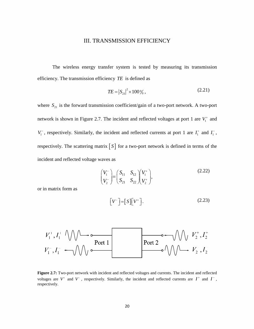
III. TRANSMISSION EFFICIENCY
The wireless energy transfer system is tested by measuring its transmission
efficiency. The transmission efficiency TE is defined as
20
021 100TE S , (2.21)
where 21S is the forward transmission coefficient/gain of a two-port network. A two-port
network is shown in Figure 2.7. The incident and reflected voltages at port 1 are 1V and
1V , respectively. Similarly, the incident and reflected currents at port 1 are 1I and 1I
,
respectively. The scattering matrix S for a two-port network is defined in terms of the
incident and reflected voltage waves as
1 1
2 2
11 12
21 22
V VS S
S SV V
,
(2.22)
or in matrix form as
V S V . (2.23)
Figure 2.7: Two-port network with incident and reflected voltages and currents. The incident and reflected
voltages are V and V
, respectively. Similarly, the incident and reflected currents are I and I
,
respectively.
21
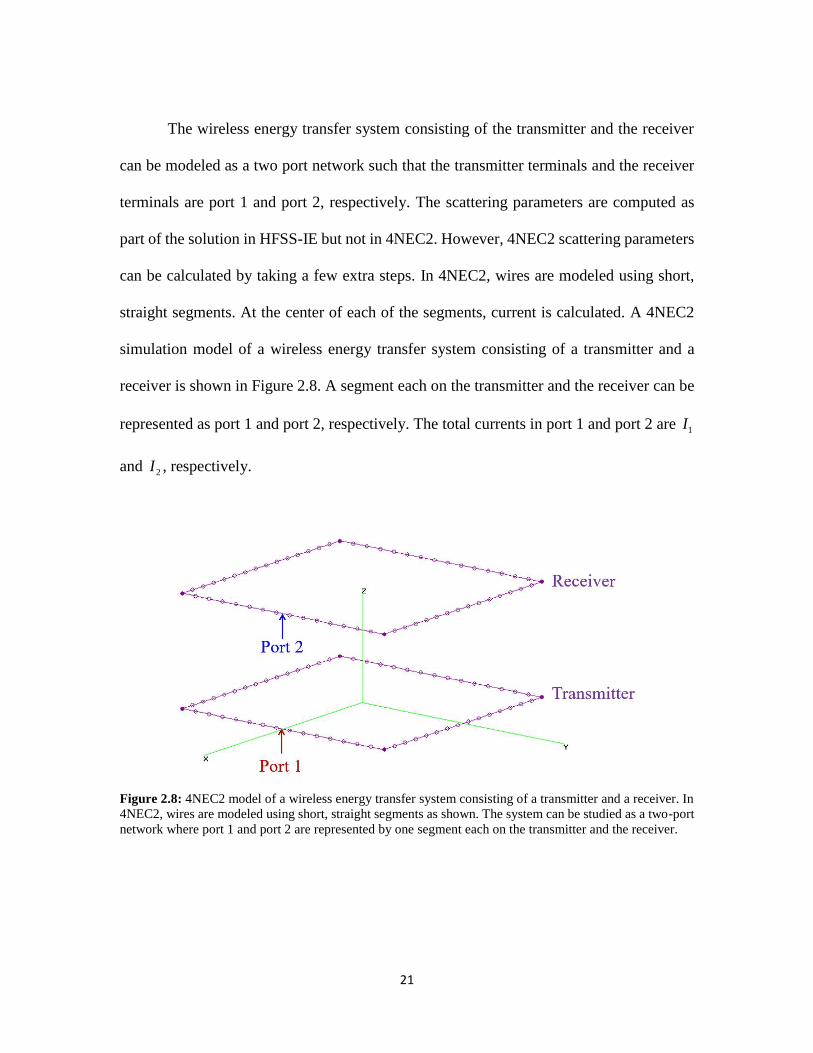
The wireless energy transfer system consisting of the transmitter and the receiver
can be modeled as a two port network such that the transmitter terminals and the receiver
terminals are port 1 and port 2, respectively. The scattering parameters are computed as
part of the solution in HFSS-IE but not in 4NEC2. However, 4NEC2 scattering parameters
can be calculated by taking a few extra steps. In 4NEC2, wires are modeled using short,
straight segments. At the center of each of the segments, current is calculated. A 4NEC2
simulation model of a wireless energy transfer system consisting of a transmitter and a
receiver is shown in Figure 2.8. A segment each on the transmitter and the receiver can be
represented as port 1 and port 2, respectively. The total currents in port 1 and port 2 are 1I
and 2I , respectively.
Figure 2.8: 4NEC2 model of a wireless energy transfer system consisting of a transmitter and a receiver. In
4NEC2, wires are modeled using short, straight segments as shown. The system can be studied as a two-port
network where port 1 and port 2 are represented by one segment each on the transmitter and the receiver.
22
The admittance matrix Y relates the total port voltages to the total port currents
as
I Y V . (2.24)
For a two-port network, the admittance parameters can be found as
0i
iij
j V
IY
V
, (2.25)
where i and j are port numbers such that 1, 2i and 1, 2j . The admittance parameters
can then be used to calculate the scattering parameters. The total voltage V and the total
current I at any port are defined as
V V V , (2.25)
0 0I I I Y V Y V , (2.26)
where V is the incident voltage, V is the reflected voltage, I is the incident current, and
I is
the reflected current. The characteristic admittance of a transmission line, 0Y is defined as
0 01Y Z where 0Z is the characteristic impedance of the same transmission line and is
defined as the ratio of voltage to current for a travelling wave on a transmission line [19].
From equations (2.24) and (2.25), the total current can be expressed as
I Y V Y V V .
(2.27)
Substituting I from equation (2.26) in equation (2.27),

23
0 0Y V Y V Y V Y V .
(2.28)
Rearranging the above equation and substituting V from equation (2.23),
0 0Y U Y V Y Y U S V , (2.29)
where U is a unit matrix. A unit matrix has equal number of rows and columns, and it
contains ones in the main diagonal and zeroes elsewhere. Dividing both sides of equation
(2.29) by V and then by 0Y U Y ,
0
0
Y U YS
Y U Y
.
(2.30)
Substituting U and Y in equation (2.30), S can be written as
1
11 12 11 12
0 0
21 22 21 22
1 0 1 0
0 1 0 1
Y Y Y YS Y Y
Y Y Y Y
.
(2.31)
Finally, the scattering matrix is expressed in terms of the admittance parameters and the
characteristic admittance of a transmission line as
0 22 0 11 12 21 0 12 11 12
0 21 0 11 0 22 12 21 21 22
21
2
Y Y Y Y Y Y Y Y S SS
Y Y Y Y Y Y Y Y S SY
.
(2.32)

24
CHAPTER 3
ANALYTICAL MODEL AND EXPERIMENTAL SETUP
For the thesis research, identical square spirals were used as the transmitter and the
receiver. Each square spiral is 50cm x 50cm and is made with copper wire of radius
0.814mmr . The choice of the wire thickness was made based on what was available in
the laboratory. Two models for wireless energy transfer were identified: basic model and
array model. The basic model consisted of the transmitter and the receiver. The array model
consisted of a 2 x 2 array of one transmitter and three parasites, and a receiver. The parasites
were identical to the transmitter but they were not connected to any power supply. A
capacitor was connected across the terminals of the parasites and the receiver. Similarly, a
capacitor in series with a power supply was connected across the transmitter terminals. The
adjacent spirals in the array model were placed 2cm apart. The dimension of the array was
102cm x 102cm which is more than twice as much in both the x- and y- directions
compared to the basic model. A network analyzer can be used to measure the scattering
parameters of the wireless energy transfer system and the transmission efficiency can be
calculated from the scattering parameters using equation (2.1). The spirals were connected
to the network analyzer using coaxial cables and the effects that these cables might have
on the experimental results were accounted for by including the cables in the simulation.
The coaxial cable connecting the transmitter to port 1 of the network analyzer was

25
approximately 75cm long, whereas the other was approximately 100cm long. The
capacitors were measured using an impedance analyzer and the measured capacitance
values were used in the simulation. The measurement results are summarized in Table 3.1.
Table 3.1: The comparison of the theoretical and measured capacitance. An impedance analyzer was used
to measure the capacitance.
As discussed earlier, the wires in 4NEC2 were modeled using short, straight
segments. In HFSS-IE, the wire was modeled as a strip. The equivalent radius r of a
narrow conducting strip is one-fourth its width w , i.e., 4r w [8]. By reciprocity, a thin
wire can be modeled as a strip of width 4w r . When 10MHzf , 30m , and
5 0.814mm 2.7 10r which implies that the wire is electrically very thin and hence
can be modeled as a strip. The HFSS-IE and 4NEC2 basic models are as shown in Figures
3.1 and 3.2, respectively.
Loop
Theoretical
Capacitance
(pF)
Measured
Capacitance
(pF)
%age
Difference
Transmitter (Tx) 22 25.2 14.5
Receiver (Rx) 22 24 9.1
18 19 5.6
Parasite 1 (Ps1) 22 23.1 5
Parasite 2 (Ps2) 22 22.9 4.1
Parasite 3 (Ps3) 22 21.9 0.5
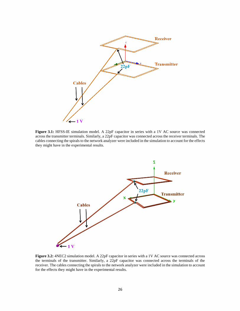
26
Figure 3.1: HFSS-IE simulation model. A 22pF capacitor in series with a 1V AC source was connected
across the transmitter terminals. Similarly, a 22pF capacitor was connected across the receiver terminals. The
cables connecting the spirals to the network analyzer were included in the simulation to account for the effects
they might have in the experimental results.
Figure 3.2: 4NEC2 simulation model. A 22pF capacitor in series with a 1V AC source was connected across
the terminals of the transmitter. Similarly, a 22pF capacitor was connected across the terminals of the
receiver. The cables connecting the spirals to the network analyzer were included in the simulation to account
for the effects they might have in the experimental results.
27
The transmitter, the receiver, and the parasites were all built on 2cm thick styrofoam
sheets. The thickness of the styrofoam sheets was not chosen for any specific reason; it was
conveniently available. However, styrofoam was chosen in the first place because it was
expected to behave much like air and have no noticeable effect on the experiment. Hence,
the thickness of the styrofoam sheet should not matter. In the basic model, the transmitter
was mounted on a 35cm tall styrofoam box. This was done in an attempt to avoid possible
coupling of the transmitter with anything that was on/under the floor. The receiver was also
mounted on a styrofoam box such that the receiver sat directly over the transmitter. The
illustration of the experimental setup of the basic model and its top view are shown in
Figure 3.3(a) and Figure 3.4, respectively. The experimental setup is shown in Figure
3.3(b).
Figure 3.3(a): Illustration of the experimental setup of the basic model. The transmitter and the receiver were
made with copper wire of radius 0.814mmr wound in clockwise direction. A 22pF capacitor in series
with a 1V AC source was connected across the transmitter terminals. Similarly, a 22pF capacitor was
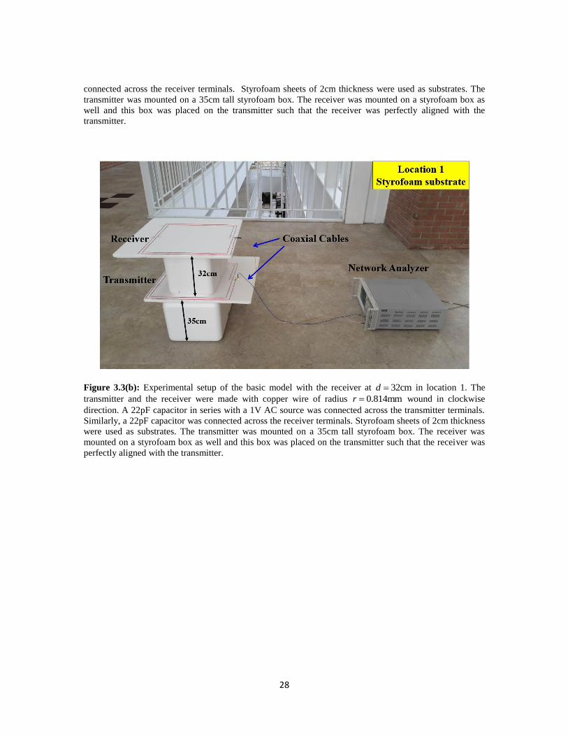
28
connected across the receiver terminals. Styrofoam sheets of 2cm thickness were used as substrates. The
transmitter was mounted on a 35cm tall styrofoam box. The receiver was mounted on a styrofoam box as
well and this box was placed on the transmitter such that the receiver was perfectly aligned with the
transmitter.
Figure 3.3(b): Experimental setup of the basic model with the receiver at 32cmd in location 1. The
transmitter and the receiver were made with copper wire of radius 0.814mmr wound in clockwise
direction. A 22pF capacitor in series with a 1V AC source was connected across the transmitter terminals.
Similarly, a 22pF capacitor was connected across the receiver terminals. Styrofoam sheets of 2cm thickness
were used as substrates. The transmitter was mounted on a 35cm tall styrofoam box. The receiver was
mounted on a styrofoam box as well and this box was placed on the transmitter such that the receiver was
perfectly aligned with the transmitter.
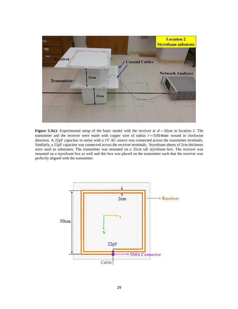
29
Figure 3.3(c): Experimental setup of the basic model with the receiver at 32cmd in location 2. The
transmitter and the receiver were made with copper wire of radius 0.814mmr wound in clockwise
direction. A 22pF capacitor in series with a 1V AC source was connected across the transmitter terminals.
Similarly, a 22pF capacitor was connected across the receiver terminals. Styrofoam sheets of 2cm thickness
were used as substrates. The transmitter was mounted on a 35cm tall styrofoam box. The receiver was
mounted on a styrofoam box as well and this box was placed on the transmitter such that the receiver was
perfectly aligned with the transmitter.
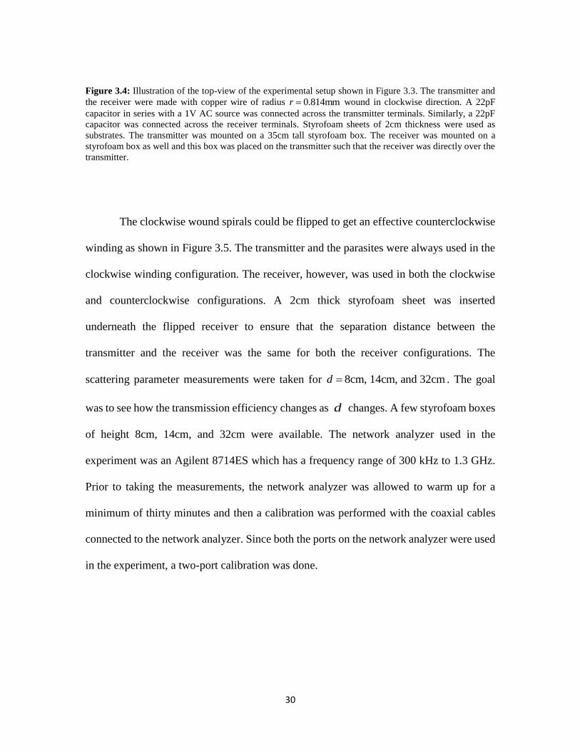
30
Figure 3.4: Illustration of the top-view of the experimental setup shown in Figure 3.3. The transmitter and
the receiver were made with copper wire of radius 0.814mmr wound in clockwise direction. A 22pF
capacitor in series with a 1V AC source was connected across the transmitter terminals. Similarly, a 22pF
capacitor was connected across the receiver terminals. Styrofoam sheets of 2cm thickness were used as
substrates. The transmitter was mounted on a 35cm tall styrofoam box. The receiver was mounted on a
styrofoam box as well and this box was placed on the transmitter such that the receiver was directly over the
transmitter.
The clockwise wound spirals could be flipped to get an effective counterclockwise
winding as shown in Figure 3.5. The transmitter and the parasites were always used in the
clockwise winding configuration. The receiver, however, was used in both the clockwise
and counterclockwise configurations. A 2cm thick styrofoam sheet was inserted
underneath the flipped receiver to ensure that the separation distance between the
transmitter and the receiver was the same for both the receiver configurations. The
scattering parameter measurements were taken for 8cm, 14cm, and 32cmd . The goal
was to see how the transmission efficiency changes as d changes. A few styrofoam boxes
of height 8cm, 14cm, and 32cm were available. The network analyzer used in the
experiment was an Agilent 8714ES which has a frequency range of 300 kHz to 1.3 GHz.
Prior to taking the measurements, the network analyzer was allowed to warm up for a
minimum of thirty minutes and then a calibration was performed with the coaxial cables
connected to the network analyzer. Since both the ports on the network analyzer were used
in the experiment, a two-port calibration was done.
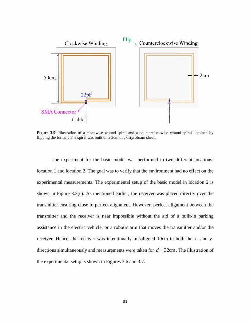
31
Figure 3.5: Illustration of a clockwise wound spiral and a counterclockwise wound spiral obtained by
flipping the former. The spiral was built on a 2cm thick styrofoam sheet.
The experiment for the basic model was performed in two different locations:
location 1 and location 2. The goal was to verify that the environment had no effect on the
experimental measurements. The experimental setup of the basic model in location 2 is
shown in Figure 3.3(c). As mentioned earlier, the receiver was placed directly over the
transmitter ensuring close to perfect alignment. However, perfect alignment between the
transmitter and the receiver is near impossible without the aid of a built-in parking
assistance in the electric vehicle, or a robotic arm that moves the transmitter and/or the
receiver. Hence, the receiver was intentionally misaligned 10cm in both the x- and y-
directions simultaneously and measurements were taken for 32cmd . The illustration of
the experimental setup is shown in Figures 3.6 and 3.7.
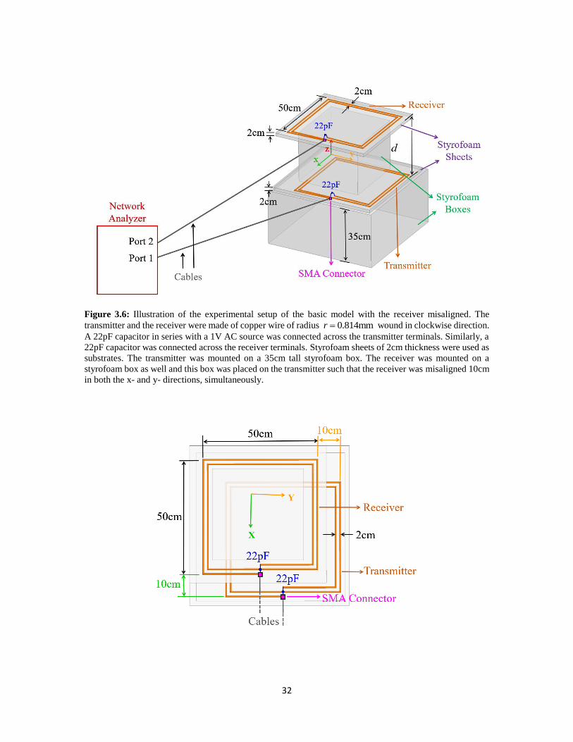
32
Figure 3.6: Illustration of the experimental setup of the basic model with the receiver misaligned. The
transmitter and the receiver were made of copper wire of radius 0.814mmr wound in clockwise direction.
A 22pF capacitor in series with a 1V AC source was connected across the transmitter terminals. Similarly, a
22pF capacitor was connected across the receiver terminals. Styrofoam sheets of 2cm thickness were used as
substrates. The transmitter was mounted on a 35cm tall styrofoam box. The receiver was mounted on a
styrofoam box as well and this box was placed on the transmitter such that the receiver was misaligned 10cm
in both the x- and y- directions, simultaneously.

33
Figure 3.7: Illustration of the top-view of the experimental setup shown in Figure 3.6 without the network
analyzer. The transmitter and the receiver were made of copper wire of radius 0.814mmr wound in
clockwise direction. A 22pF capacitor in series with a 1V AC source was connected across the transmitter
terminals. Similarly, a 22pF capacitor was connected across the receiver terminals. Styrofoam sheets of 2cm
thickness were used as substrates. The transmitter was mounted on a 35cm tall styrofoam box. The receiver
was mounted on a styrofoam box as well and this box was placed on the transmitter such that the receiver
was misaligned 10cm in both the x- and y- directions, simultaneously.
The reproducibility of the basic model experiment was confirmed by building
another set of transmitter and receiver on a 3mm thick cardboard substrate. As in the
experiment with the styrofoam substrate, the transmitter was mounted on a 35cm tall
styrofoam box. The receiver was also mounted on a styrofoam box such that the receiver
sat directly over the transmitter. A 2cm thick styrofoam sheet was inserted underneath the
cardboard substrate containing the receiver to ensure that d was the same for the
experimental setups with the styrofoam and the cardboard substrates. The thickness of the
cardboard substrate was assumed to be negligible to simplify the experiment. The
illustration of the experimental setup of the basic model with the cardboard substrates is
shown in Figure 3.8(a). The experimental setup is shown in Figure 3.8(b).
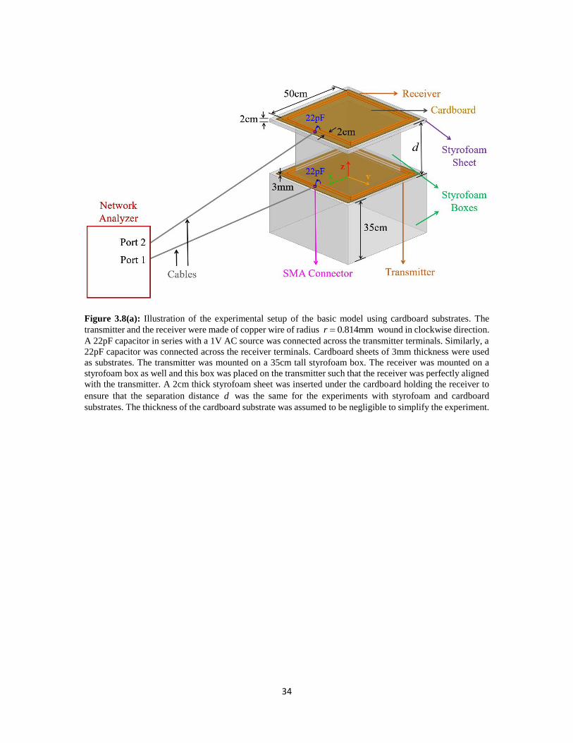
34
Figure 3.8(a): Illustration of the experimental setup of the basic model using cardboard substrates. The
transmitter and the receiver were made of copper wire of radius 0.814mmr wound in clockwise direction.
A 22pF capacitor in series with a 1V AC source was connected across the transmitter terminals. Similarly, a
22pF capacitor was connected across the receiver terminals. Cardboard sheets of 3mm thickness were used
as substrates. The transmitter was mounted on a 35cm tall styrofoam box. The receiver was mounted on a
styrofoam box as well and this box was placed on the transmitter such that the receiver was perfectly aligned
with the transmitter. A 2cm thick styrofoam sheet was inserted under the cardboard holding the receiver to
ensure that the separation distance d was the same for the experiments with styrofoam and cardboard
substrates. The thickness of the cardboard substrate was assumed to be negligible to simplify the experiment.
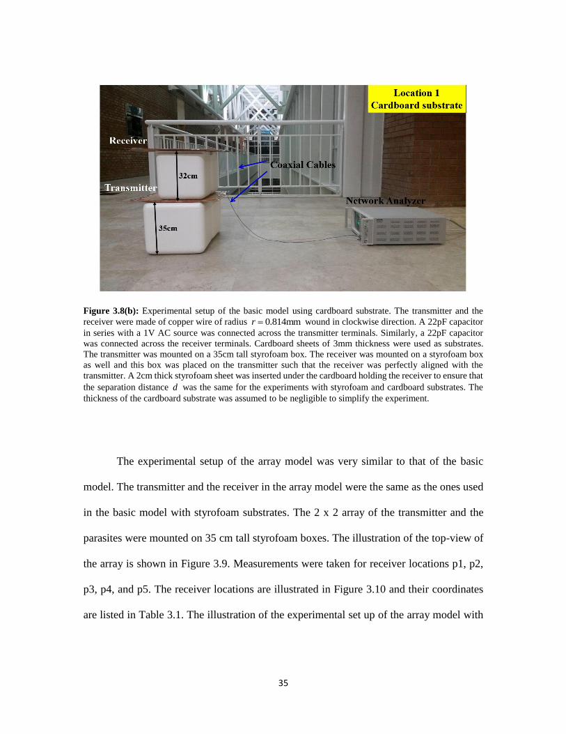
35
Figure 3.8(b): Experimental setup of the basic model using cardboard substrate. The transmitter and the
receiver were made of copper wire of radius 0.814mmr wound in clockwise direction. A 22pF capacitor
in series with a 1V AC source was connected across the transmitter terminals. Similarly, a 22pF capacitor
was connected across the receiver terminals. Cardboard sheets of 3mm thickness were used as substrates.
The transmitter was mounted on a 35cm tall styrofoam box. The receiver was mounted on a styrofoam box
as well and this box was placed on the transmitter such that the receiver was perfectly aligned with the
transmitter. A 2cm thick styrofoam sheet was inserted under the cardboard holding the receiver to ensure that
the separation distance d was the same for the experiments with styrofoam and cardboard substrates. The
thickness of the cardboard substrate was assumed to be negligible to simplify the experiment.
The experimental setup of the array model was very similar to that of the basic
model. The transmitter and the receiver in the array model were the same as the ones used
in the basic model with styrofoam substrates. The 2 x 2 array of the transmitter and the
parasites were mounted on 35 cm tall styrofoam boxes. The illustration of the top-view of
the array is shown in Figure 3.9. Measurements were taken for receiver locations p1, p2,
p3, p4, and p5. The receiver locations are illustrated in Figure 3.10 and their coordinates
are listed in Table 3.1. The illustration of the experimental set up of the array model with
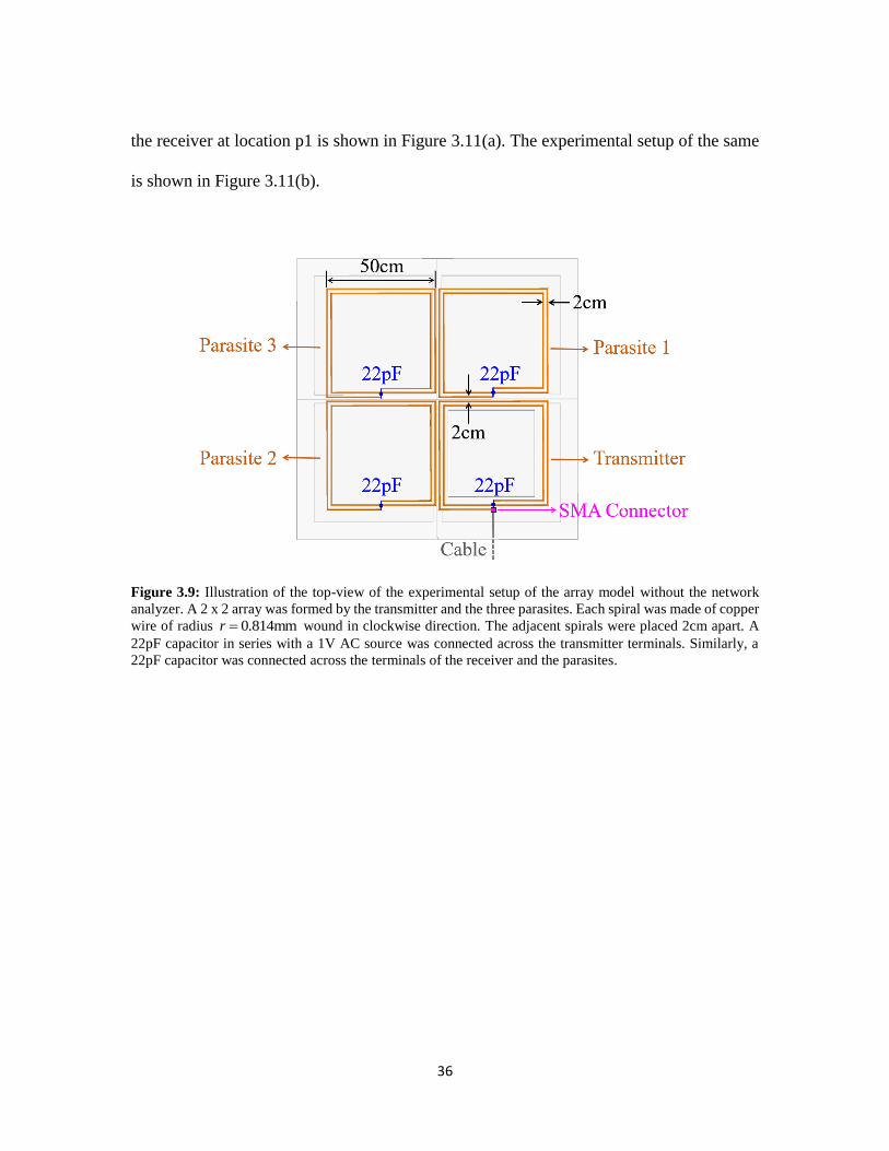
36
the receiver at location p1 is shown in Figure 3.11(a). The experimental setup of the same
is shown in Figure 3.11(b).
Figure 3.9: Illustration of the top-view of the experimental setup of the array model without the network
analyzer. A 2 x 2 array was formed by the transmitter and the three parasites. Each spiral was made of copper
wire of radius 0.814mmr wound in clockwise direction. The adjacent spirals were placed 2cm apart. A
22pF capacitor in series with a 1V AC source was connected across the transmitter terminals. Similarly, a
22pF capacitor was connected across the terminals of the receiver and the parasites.
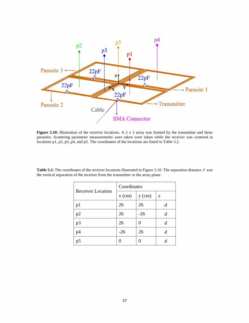
37
Figure 3.10: Illustration of the receiver locations. A 2 x 2 array was formed by the transmitter and three
parasites. Scattering parameter measurements were taken were taken while the receiver was centered at
locations p1, p2, p3, p4, and p5. The coordinates of the locations are listed in Table 3.2.
Table 3.2: The coordinates of the receiver locations illustrated in Figure 3.10. The separation distance d was
the vertical separation of the receiver from the transmitter or the array plane.
Receiver Location Coordinates
x (cm) y (cm) z
p1 26 26 𝑑
p2 26 -26 𝑑
p3 26 0 𝑑
p4 -26 26 𝑑
p5 0 0 𝑑
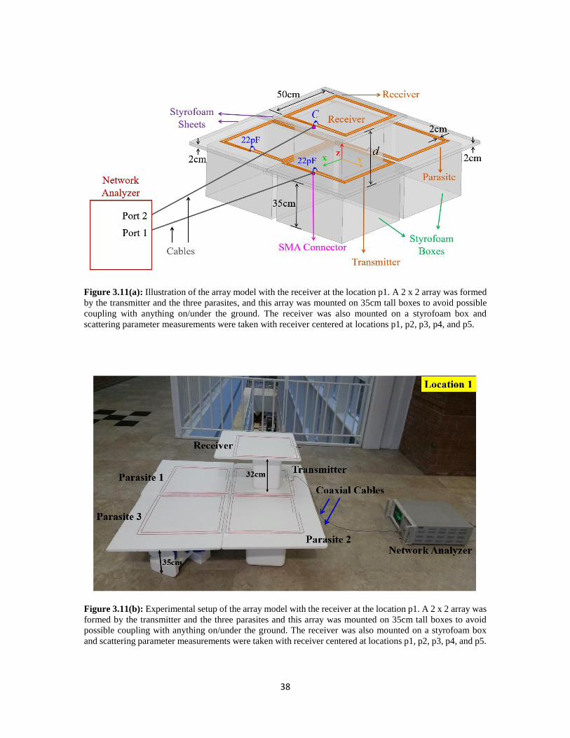
38
Figure 3.11(a): Illustration of the array model with the receiver at the location p1. A 2 x 2 array was formed
by the transmitter and the three parasites, and this array was mounted on 35cm tall boxes to avoid possible
coupling with anything on/under the ground. The receiver was also mounted on a styrofoam box and
scattering parameter measurements were taken with receiver centered at locations p1, p2, p3, p4, and p5.
Figure 3.11(b): Experimental setup of the array model with the receiver at the location p1. A 2 x 2 array was
formed by the transmitter and the three parasites and this array was mounted on 35cm tall boxes to avoid
possible coupling with anything on/under the ground. The receiver was also mounted on a styrofoam box
and scattering parameter measurements were taken with receiver centered at locations p1, p2, p3, p4, and p5.
39
CHAPTER 4
RESULTS AND DISCUSSIONS
I. Basic Model: Location 1, Styrofoam Substrate
The scattering parameters of the basic model in location 1 were measured for
separation distance 8cm, 14cm, and 32cmd . The transmission efficiency versus
frequency plots obtained from HFSS-IE and 4NEC2 simulations were very similar to each
other. The experimental measurements agreed well with the simulations for
counterclockwise wound receiver (RxCCW). However, for clockwise wound receiver
(RxCW), the measurements did not agree well with the simulations. As was discussed
earlier in Chapter 3, the coupling coefficient k increases as the separation distance d
between the transmitter and the receiver decreases. Increasing k past the critical value
causes double humps to appear in the receiver current and the induced emf plots. Further
increasing k causes the double humps to get farther apart. This trend was seen in the
simulation as well as the measurement results. These results are shown in Figures 4.1
through 4.6.
Ideally, the spirals and the capacitors would be perfect, the coaxial cables
connecting the transmitter and the receiver to the network analyzer would have no effect
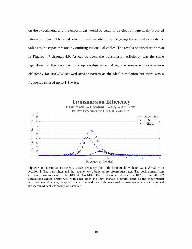
40
on the experiment, and the experiment would be setup in an electromagnetically isolated
laboratory space. The ideal situation was simulated by assigning theoretical capacitance
values to the capacitors and by omitting the coaxial cables. The results obtained are shown
in Figures 4.7 through 4.9. As can be seen, the transmission efficiency was the same
regardless of the receiver winding configuration. Also, the measured transmission
efficiency for RxCCW showed similar pattern as the ideal simulation but there was a
frequency shift of up to 1.5 MHz.
Figure 4.1: Transmission efficiency versus frequency plot of the basic model with RxCW at 32cmd in
location 1. The transmitter and the receiver were built on styrofoam substrates. The peak transmission
efficiency was measured to be 10% at 11.4 MHz. The results obtained from the HFSS-IE and 4NEC2
simulations agreed pretty well with each other and they showed a similar trend as the experimental
measurement. However, compared to the simulated results, the measured resonant frequency was larger and
the measured peak efficiency was smaller.
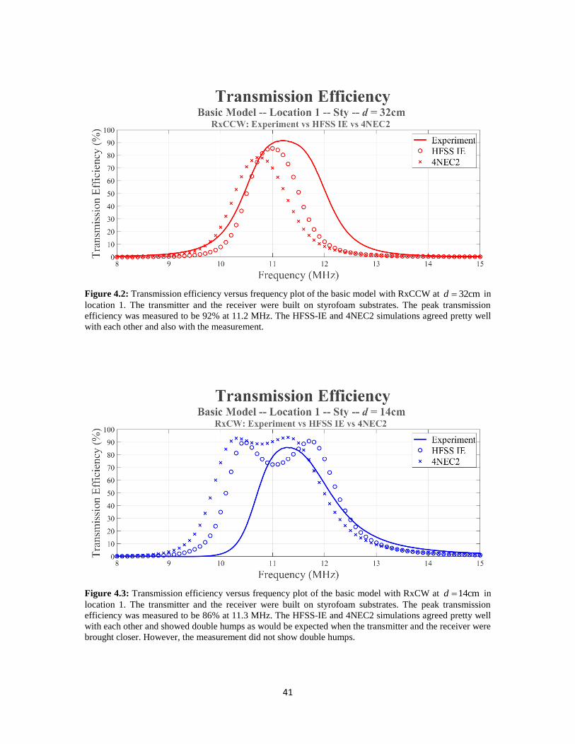
41
Figure 4.2: Transmission efficiency versus frequency plot of the basic model with RxCCW at 32cmd in
location 1. The transmitter and the receiver were built on styrofoam substrates. The peak transmission
efficiency was measured to be 92% at 11.2 MHz. The HFSS-IE and 4NEC2 simulations agreed pretty well
with each other and also with the measurement.
Figure 4.3: Transmission efficiency versus frequency plot of the basic model with RxCW at 14cmd in
location 1. The transmitter and the receiver were built on styrofoam substrates. The peak transmission
efficiency was measured to be 86% at 11.3 MHz. The HFSS-IE and 4NEC2 simulations agreed pretty well
with each other and showed double humps as would be expected when the transmitter and the receiver were
brought closer. However, the measurement did not show double humps.
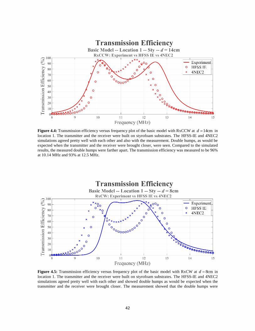
42
Figure 4.4: Transmission efficiency versus frequency plot of the basic model with RxCCW at 14cmd in
location 1. The transmitter and the receiver were built on styrofoam substrates. The HFSS-IE and 4NEC2
simulations agreed pretty well with each other and also with the measurement. Double humps, as would be
expected when the transmitter and the receiver were brought closer, were seen. Compared to the simulated
results, the measured double humps were farther apart. The transmission efficiency was measured to be 96%
at 10.14 MHz and 93% at 12.5 MHz.
Figure 4.5: Transmission efficiency versus frequency plot of the basic model with RxCW at 8cmd in
location 1. The transmitter and the receiver were built on styrofoam substrates. The HFSS-IE and 4NEC2
simulations agreed pretty well with each other and showed double humps as would be expected when the
transmitter and the receiver were brought closer. The measurement showed that the double humps were
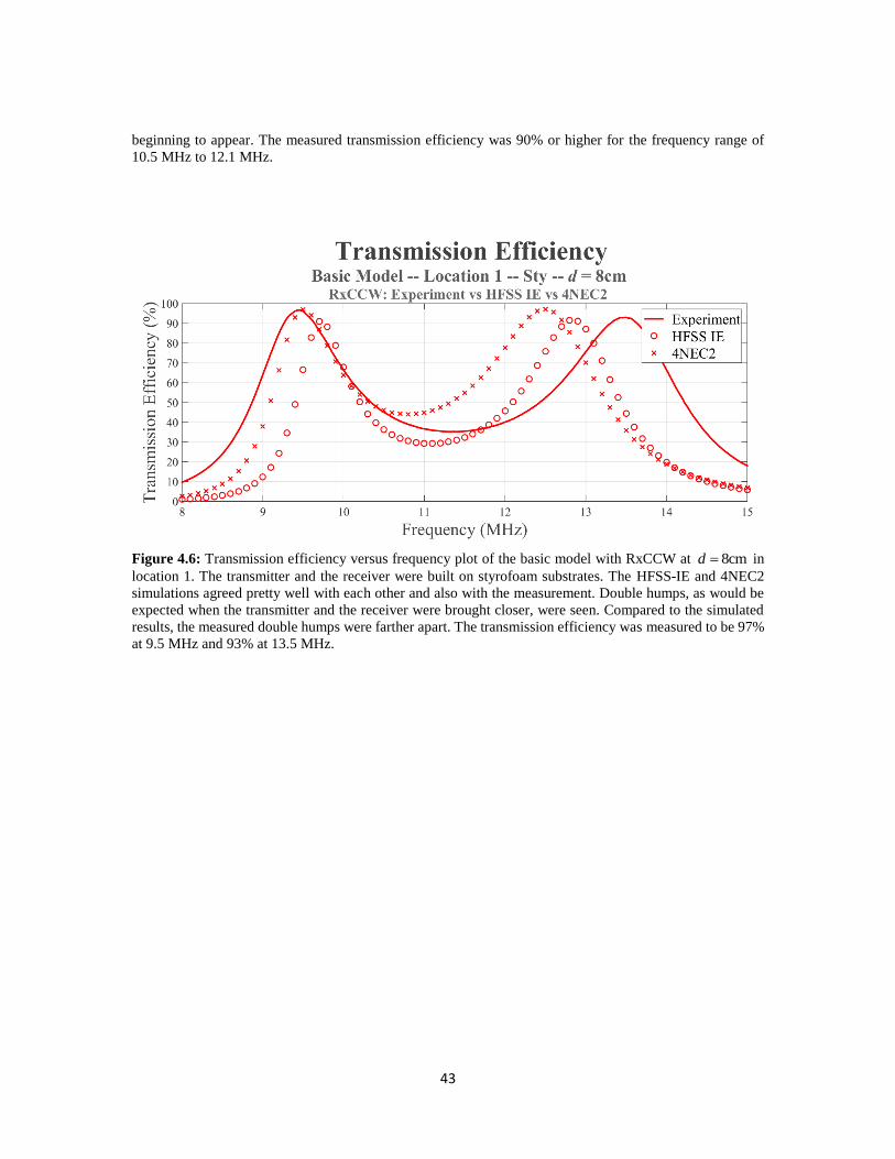
43
beginning to appear. The measured transmission efficiency was 90% or higher for the frequency range of
10.5 MHz to 12.1 MHz.
Figure 4.6: Transmission efficiency versus frequency plot of the basic model with RxCCW at 8cmd in
location 1. The transmitter and the receiver were built on styrofoam substrates. The HFSS-IE and 4NEC2
simulations agreed pretty well with each other and also with the measurement. Double humps, as would be
expected when the transmitter and the receiver were brought closer, were seen. Compared to the simulated
results, the measured double humps were farther apart. The transmission efficiency was measured to be 97%
at 9.5 MHz and 93% at 13.5 MHz.
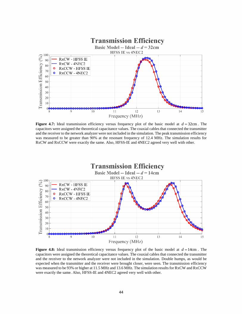
44
Figure 4.7: Ideal transmission efficiency versus frequency plot of the basic model at 32cmd . The
capacitors were assigned the theoretical capacitance values. The coaxial cables that connected the transmitter
and the receiver to the network analyzer were not included in the simulation. The peak transmission efficiency
was measured to be greater than 90% at the resonant frequency of 12.4 MHz. The simulation results for
RxCW and RxCCW were exactly the same. Also, HFSS-IE and 4NEC2 agreed very well with other.
Figure 4.8: Ideal transmission efficiency versus frequency plot of the basic model at 14cmd . The
capacitors were assigned the theoretical capacitance values. The coaxial cables that connected the transmitter
and the receiver to the network analyzer were not included in the simulation. Double humps, as would be
expected when the transmitter and the receiver were brought closer, were seen. The transmission efficiency
was measured to be 93% or higher at 11.5 MHz and 13.6 MHz. The simulation results for RxCW and RxCCW
were exactly the same. Also, HFSS-IE and 4NEC2 agreed very well with other.
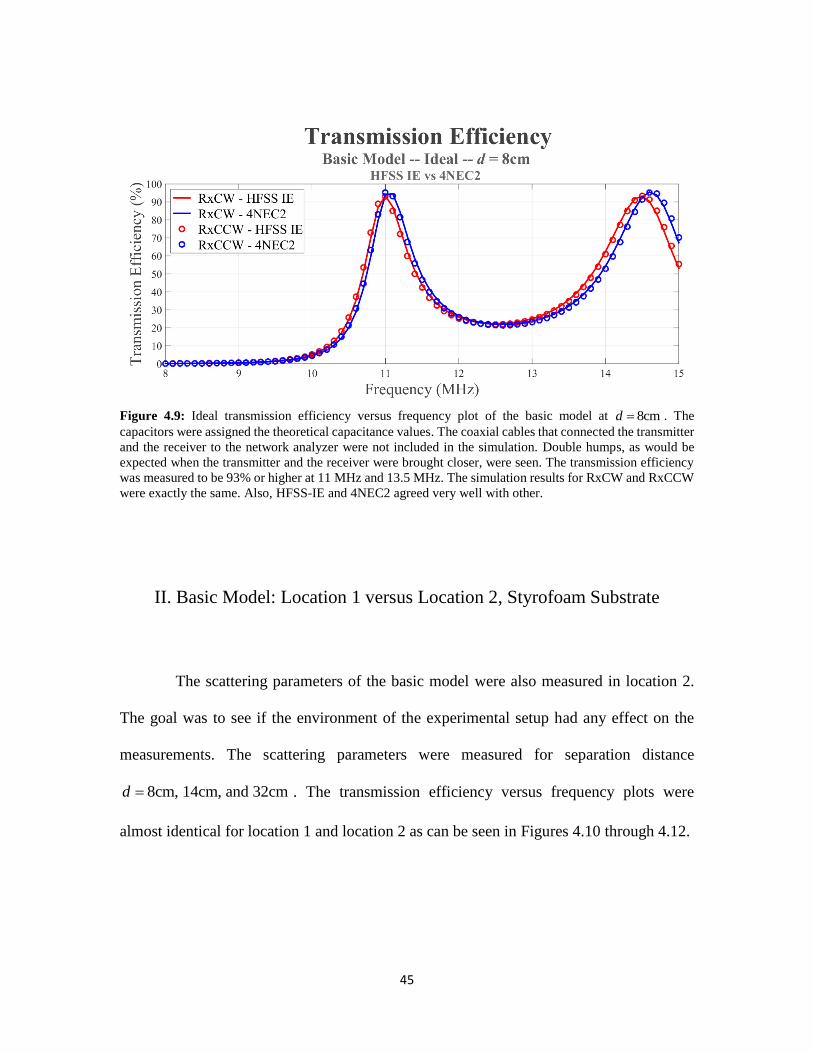
45
Figure 4.9: Ideal transmission efficiency versus frequency plot of the basic model at 8cmd . The
capacitors were assigned the theoretical capacitance values. The coaxial cables that connected the transmitter
and the receiver to the network analyzer were not included in the simulation. Double humps, as would be
expected when the transmitter and the receiver were brought closer, were seen. The transmission efficiency
was measured to be 93% or higher at 11 MHz and 13.5 MHz. The simulation results for RxCW and RxCCW
were exactly the same. Also, HFSS-IE and 4NEC2 agreed very well with other.
II. Basic Model: Location 1 versus Location 2, Styrofoam Substrate
The scattering parameters of the basic model were also measured in location 2.
The goal was to see if the environment of the experimental setup had any effect on the
measurements. The scattering parameters were measured for separation distance
8cm, 14cm, and 32cmd . The transmission efficiency versus frequency plots were
almost identical for location 1 and location 2 as can be seen in Figures 4.10 through 4.12.
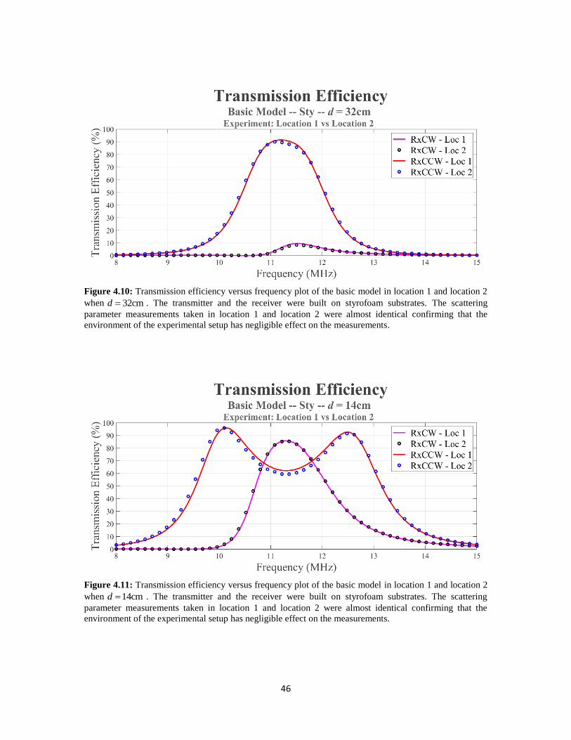
46
Figure 4.10: Transmission efficiency versus frequency plot of the basic model in location 1 and location 2
when 32cmd . The transmitter and the receiver were built on styrofoam substrates. The scattering
parameter measurements taken in location 1 and location 2 were almost identical confirming that the
environment of the experimental setup has negligible effect on the measurements.
Figure 4.11: Transmission efficiency versus frequency plot of the basic model in location 1 and location 2
when 14cmd . The transmitter and the receiver were built on styrofoam substrates. The scattering
parameter measurements taken in location 1 and location 2 were almost identical confirming that the
environment of the experimental setup has negligible effect on the measurements.
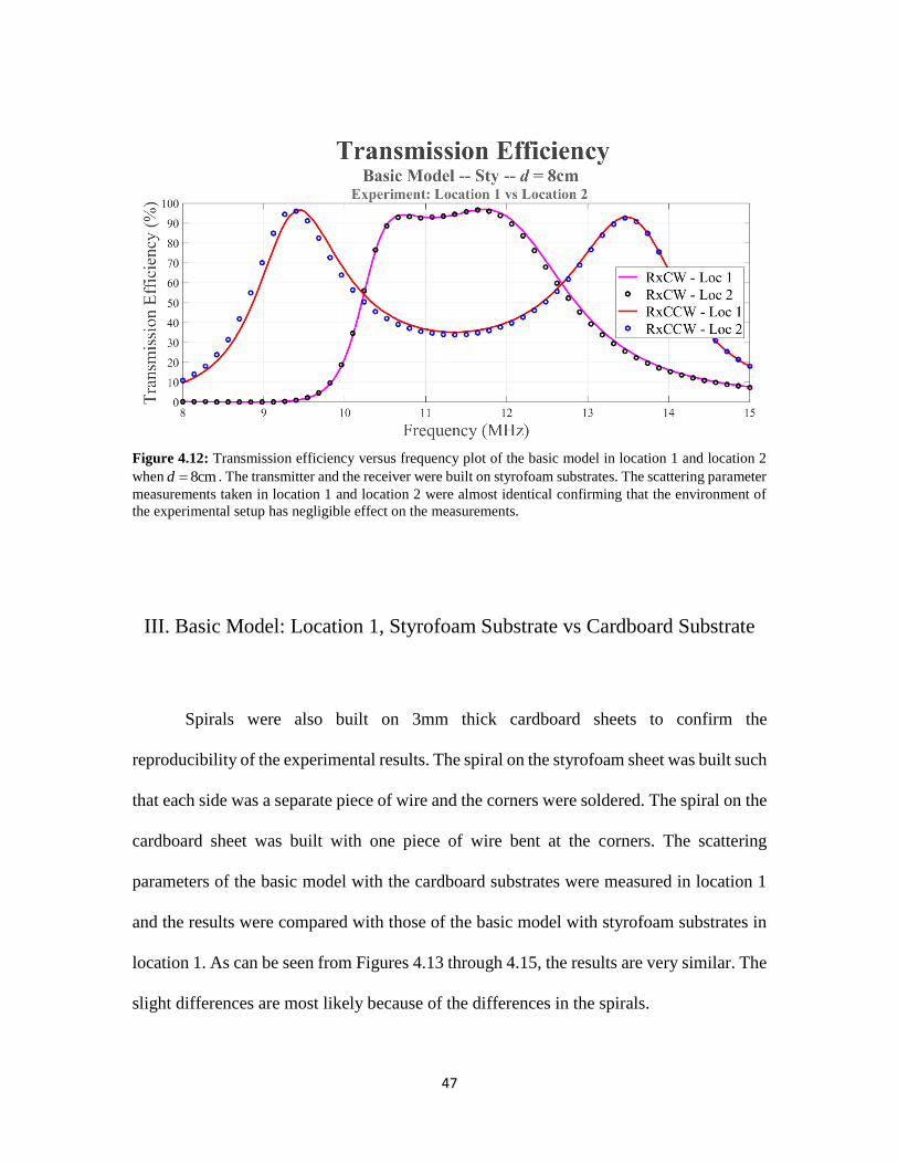
47
Figure 4.12: Transmission efficiency versus frequency plot of the basic model in location 1 and location 2
when 8cmd . The transmitter and the receiver were built on styrofoam substrates. The scattering parameter
measurements taken in location 1 and location 2 were almost identical confirming that the environment of
the experimental setup has negligible effect on the measurements.
III. Basic Model: Location 1, Styrofoam Substrate vs Cardboard Substrate
Spirals were also built on 3mm thick cardboard sheets to confirm the
reproducibility of the experimental results. The spiral on the styrofoam sheet was built such
that each side was a separate piece of wire and the corners were soldered. The spiral on the
cardboard sheet was built with one piece of wire bent at the corners. The scattering
parameters of the basic model with the cardboard substrates were measured in location 1
and the results were compared with those of the basic model with styrofoam substrates in
location 1. As can be seen from Figures 4.13 through 4.15, the results are very similar. The
slight differences are most likely because of the differences in the spirals.
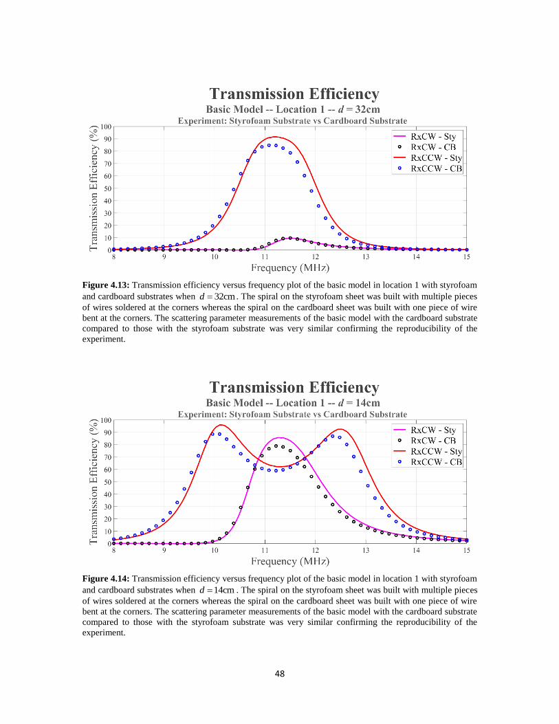
48
Figure 4.13: Transmission efficiency versus frequency plot of the basic model in location 1 with styrofoam
and cardboard substrates when 32cmd . The spiral on the styrofoam sheet was built with multiple pieces
of wires soldered at the corners whereas the spiral on the cardboard sheet was built with one piece of wire
bent at the corners. The scattering parameter measurements of the basic model with the cardboard substrate
compared to those with the styrofoam substrate was very similar confirming the reproducibility of the
experiment.
Figure 4.14: Transmission efficiency versus frequency plot of the basic model in location 1 with styrofoam
and cardboard substrates when 14cmd . The spiral on the styrofoam sheet was built with multiple pieces
of wires soldered at the corners whereas the spiral on the cardboard sheet was built with one piece of wire
bent at the corners. The scattering parameter measurements of the basic model with the cardboard substrate
compared to those with the styrofoam substrate was very similar confirming the reproducibility of the
experiment.
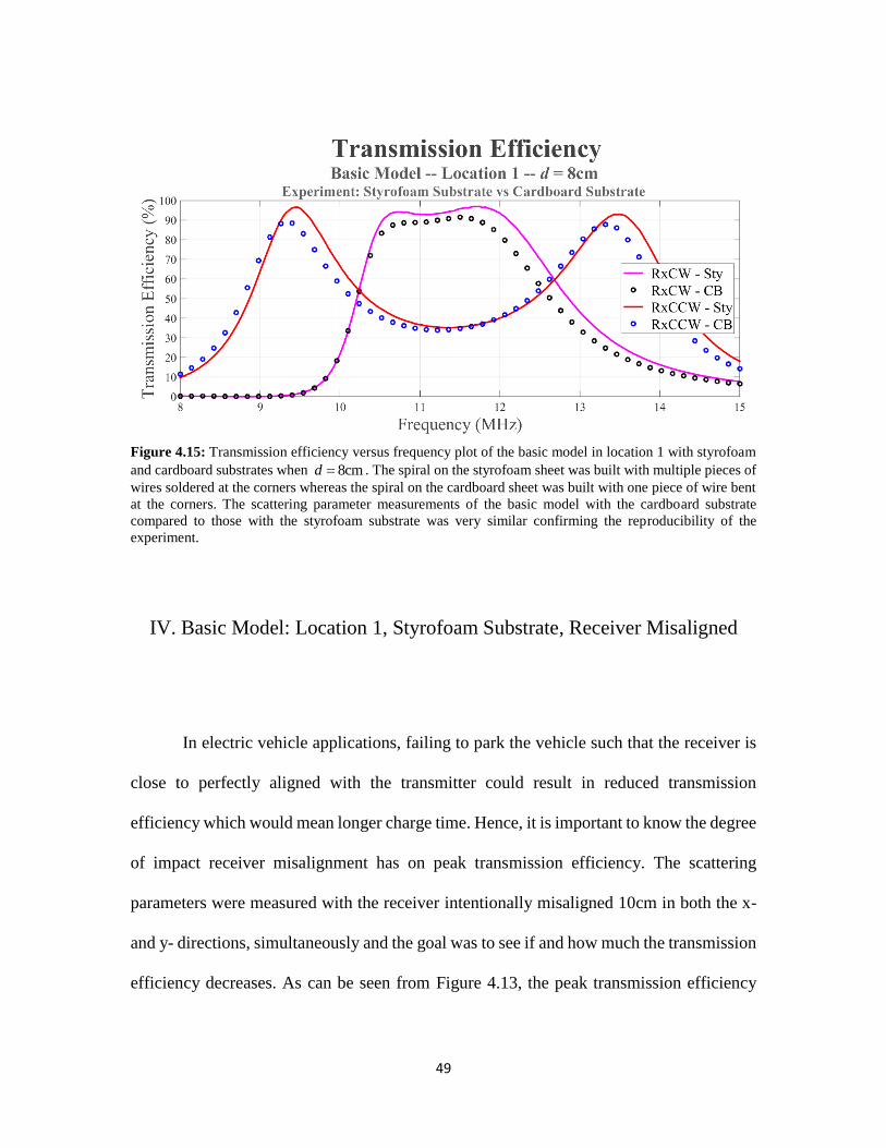
49
Figure 4.15: Transmission efficiency versus frequency plot of the basic model in location 1 with styrofoam
and cardboard substrates when 8cmd . The spiral on the styrofoam sheet was built with multiple pieces of
wires soldered at the corners whereas the spiral on the cardboard sheet was built with one piece of wire bent
at the corners. The scattering parameter measurements of the basic model with the cardboard substrate
compared to those with the styrofoam substrate was very similar confirming the reproducibility of the
experiment.
IV. Basic Model: Location 1, Styrofoam Substrate, Receiver Misaligned
In electric vehicle applications, failing to park the vehicle such that the receiver is
close to perfectly aligned with the transmitter could result in reduced transmission
efficiency which would mean longer charge time. Hence, it is important to know the degree
of impact receiver misalignment has on peak transmission efficiency. The scattering
parameters were measured with the receiver intentionally misaligned 10cm in both the x-
and y- directions, simultaneously and the goal was to see if and how much the transmission
efficiency decreases. As can be seen from Figure 4.13, the peak transmission efficiency
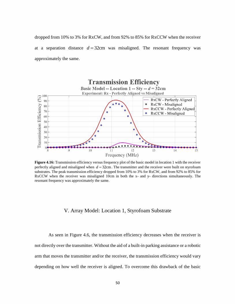
50
dropped from 10% to 3% for RxCW, and from 92% to 85% for RxCCW when the receiver
at a separation distance 32cmd was misaligned. The resonant frequency was
approximately the same.
Figure 4.16: Transmission efficiency versus frequency plot of the basic model in location 1 with the receiver
perfectly aligned and misaligned when 32cmd . The transmitter and the receiver were built on styrofoam
substrates. The peak transmission efficiency dropped from 10% to 3% for RxCW, and from 92% to 85% for
RxCCW when the receiver was misaligned 10cm in both the x- and y- directions simultaneously. The
resonant frequency was approximately the same.
V. Array Model: Location 1, Styrofoam Substrate
As seen in Figure 4.6, the transmission efficiency decreases when the receiver is
not directly over the transmitter. Without the aid of a built-in parking assistance or a robotic
arm that moves the transmitter and/or the receiver, the transmission efficiency would vary
depending on how well the receiver is aligned. To overcome this drawback of the basic

51
model, the array model was designed. A 2 x 2 array was formed by the transmitter and the
parasites, and the receiver was placed 32cm over the array plane. A 22pF capacitor was
connected across the terminals of each parasite and the receiver as well. Similarly, a 22pF
capacitor in series with a 1V AC source was connected across the transmitter terminals.
The scattering parameter measurements were taken with the receiver centered at locations
p1, p2, p3, p4, and p5. The coordinates of these locations are listed in Table 3.2. As can be
seen from Figures 4.18 and 4.19, the transmission efficiency was the least sensitive to
receiver location when the operating frequency was 13.36 MHz for RxCW and 13.39 MHz
for RxCCW. At 13.36 MHz, the transmission efficiency ranged from 3% to 20% for
RxCW. Similarly, at 13.39 MHz, the transmission efficiency ranged from 14% to 35% for
RxCCW. For the basic model with the receiver at 32cmd , the transmission efficiency
was the maximum at 11.12 MHz. However, for the array model with the receiver at
32cmd , the transmission efficiency at/around 11.12 MHz varied largely with the
receiver location. For RxCW, the transmission efficiency ranged from 6% to 45% and for
RxCCW, it ranged from 2% to 84%. By operating the array model at the frequency where
the transmission efficiency is the least sensitive to receiver position, the reliability of the
model can be improved. Furthermore, the receiver can be tuned to resonate at this
frequency of least sensitivity which could improve the transmission efficiency. Hence, an
18pF capacitor was connected across the receiver terminals and the scattering parameter
measurements were taken for receiver locations p1, p2, p3, p4, and p5. The results are
shown in Figures 4.19 and 4.20. At 13.36 MHz, the transmission efficiency for RxCW
improved for all locations except p1. This resulted in an even larger variation in
52
transmission efficiency, and as discussed earlier, this outcome is highly undesired.
However, for RxCCW, the transmission efficiency improved for all the receiver locations
and ranged from 33% to 56%.
To sum up, the basic model with RxCCW resulted in a larger transmission
efficiency compared to the array model. However, the array model provided more freedom
for receiver placement. Hence, the choice of the model is a trade-off between the
transmission efficiency and the freedom for receiver placement. As was discussed earlier,
the transmission efficiency of the basic model decreased only slightly when the receiver
was misaligned. An electric vehicle with a built-in parking assistance, or a robotic arm that
moves the transmitter and/or the receiver would be a solution to the receiver misalignment
problem making the basic model a clear winner.
The experimental results of the array model are shown in Figures 4.17 through 4.20.
Originally, a 22pF capacitor was connected across the receiver terminal so that the receiver
resonated at the same frequency as the transmitter and the parasites. Later, an 18pF
capacitor was connected across the receiver terminal off-tune it. In the Figures 4.17 through
4.22, the plot titles say “resonance” if the receiver resonated at the same frequency as the
transmitter and the parasites, and “off-resonance” if the receiver was off-tuned.
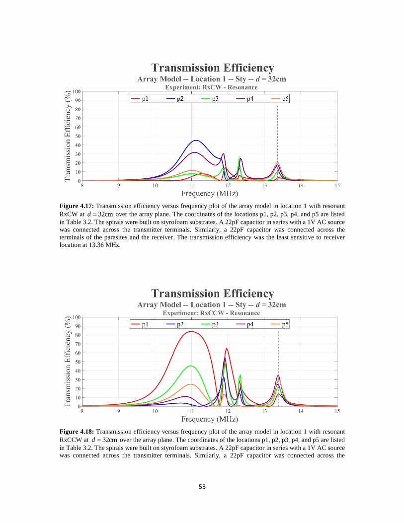
53
Figure 4.17: Transmission efficiency versus frequency plot of the array model in location 1 with resonant
RxCW at 32cmd over the array plane. The coordinates of the locations p1, p2, p3, p4, and p5 are listed
in Table 3.2. The spirals were built on styrofoam substrates. A 22pF capacitor in series with a 1V AC source
was connected across the transmitter terminals. Similarly, a 22pF capacitor was connected across the
terminals of the parasites and the receiver. The transmission efficiency was the least sensitive to receiver
location at 13.36 MHz.
Figure 4.18: Transmission efficiency versus frequency plot of the array model in location 1 with resonant
RxCCW at 32cmd over the array plane. The coordinates of the locations p1, p2, p3, p4, and p5 are listed
in Table 3.2. The spirals were built on styrofoam substrates. A 22pF capacitor in series with a 1V AC source
was connected across the transmitter terminals. Similarly, a 22pF capacitor was connected across the
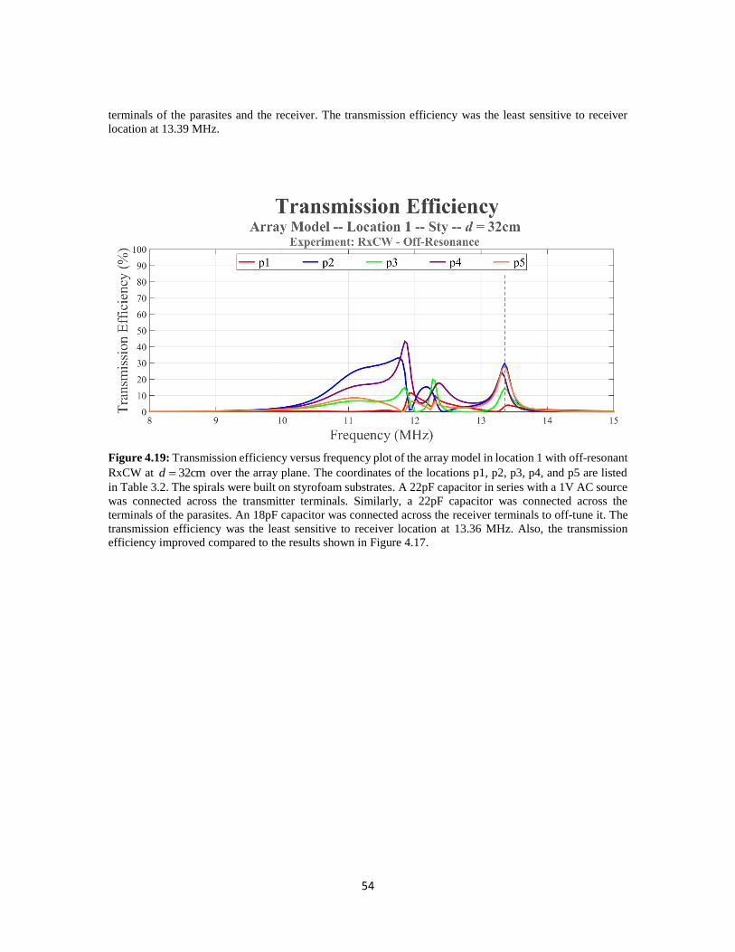
54
terminals of the parasites and the receiver. The transmission efficiency was the least sensitive to receiver
location at 13.39 MHz.
Figure 4.19: Transmission efficiency versus frequency plot of the array model in location 1 with off-resonant
RxCW at 32cmd over the array plane. The coordinates of the locations p1, p2, p3, p4, and p5 are listed
in Table 3.2. The spirals were built on styrofoam substrates. A 22pF capacitor in series with a 1V AC source
was connected across the transmitter terminals. Similarly, a 22pF capacitor was connected across the
terminals of the parasites. An 18pF capacitor was connected across the receiver terminals to off-tune it. The
transmission efficiency was the least sensitive to receiver location at 13.36 MHz. Also, the transmission
efficiency improved compared to the results shown in Figure 4.17.
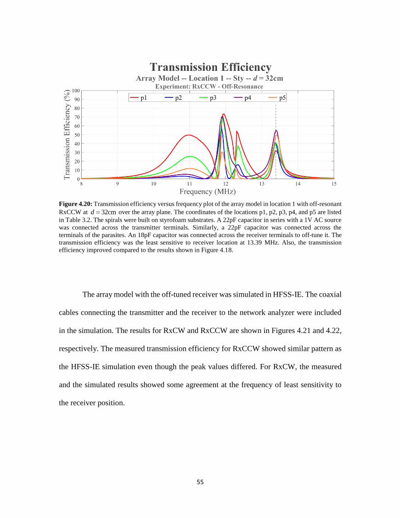
55
Figure 4.20: Transmission efficiency versus frequency plot of the array model in location 1 with off-resonant
RxCCW at 32cmd over the array plane. The coordinates of the locations p1, p2, p3, p4, and p5 are listed
in Table 3.2. The spirals were built on styrofoam substrates. A 22pF capacitor in series with a 1V AC source
was connected across the transmitter terminals. Similarly, a 22pF capacitor was connected across the
terminals of the parasites. An 18pF capacitor was connected across the receiver terminals to off-tune it. The
transmission efficiency was the least sensitive to receiver location at 13.39 MHz. Also, the transmission
efficiency improved compared to the results shown in Figure 4.18.
The array model with the off-tuned receiver was simulated in HFSS-IE. The coaxial
cables connecting the transmitter and the receiver to the network analyzer were included
in the simulation. The results for RxCW and RxCCW are shown in Figures 4.21 and 4.22,
respectively. The measured transmission efficiency for RxCCW showed similar pattern as
the HFSS-IE simulation even though the peak values differed. For RxCW, the measured
and the simulated results showed some agreement at the frequency of least sensitivity to
the receiver position.
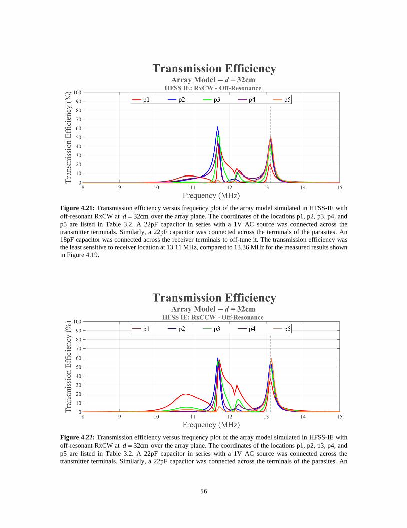
56
Figure 4.21: Transmission efficiency versus frequency plot of the array model simulated in HFSS-IE with
off-resonant RxCW at 32cmd over the array plane. The coordinates of the locations p1, p2, p3, p4, and
p5 are listed in Table 3.2. A 22pF capacitor in series with a 1V AC source was connected across the
transmitter terminals. Similarly, a 22pF capacitor was connected across the terminals of the parasites. An
18pF capacitor was connected across the receiver terminals to off-tune it. The transmission efficiency was
the least sensitive to receiver location at 13.11 MHz, compared to 13.36 MHz for the measured results shown
in Figure 4.19.
Figure 4.22: Transmission efficiency versus frequency plot of the array model simulated in HFSS-IE with
off-resonant RxCW at 32cmd over the array plane. The coordinates of the locations p1, p2, p3, p4, and
p5 are listed in Table 3.2. A 22pF capacitor in series with a 1V AC source was connected across the
transmitter terminals. Similarly, a 22pF capacitor was connected across the terminals of the parasites. An

57
18pF capacitor was connected across the receiver terminals to off-tune it. The transmission efficiency was
the least sensitive to receiver location at 13.11 MHz, compared to 13.39 MHz for the measured results as
shown in Figure 4.20.
HFSS-IE simulation was performed with an ideal array model. Ideally, the spirals
and the capacitors would be perfect, the coaxial cables connecting the transmitter and the
receiver to the network analyzer would have no effect on the experiment, and the
experiment would be setup in an electromagnetically isolated laboratory space. The results
of the ideal array model simulation are shown in Figures 4.23 and 4.24. The transmission
efficiency is the least sensitive to receiver position at 13.46 MHz. Tuning the receiver such
that it resonated at 13.46 MHz helped improve the transmission efficiency. As can be seen,
the transmission efficiency was 75% or higher at 13.46 MHz. Also, compared to the non-
ideal simulation and the measurement, the curve was flatter. A steep curve is less desirable
since that means an accurate frequency control mechanism is required to ensure the peak
transmission efficiency.
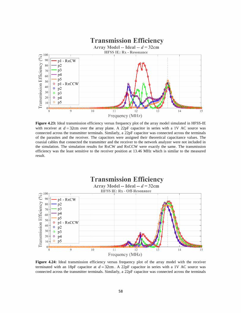
58
Figure 4.23: Ideal transmission efficiency versus frequency plot of the array model simulated in HFSS-IE
with receiver at 32cmd over the array plane. A 22pF capacitor in series with a 1V AC source was
connected across the transmitter terminals. Similarly, a 22pF capacitor was connected across the terminals
of the parasites and the receiver. The capacitors were assigned their theoretical capacitance values. The
coaxial cables that connected the transmitter and the receiver to the network analyzer were not included in
the simulation. The simulation results for RxCW and RxCCW were exactly the same. The transmission
efficiency was the least sensitive to the receiver position at 13.46 MHz which is similar to the measured
result.
Figure 4.24: Ideal transmission efficiency versus frequency plot of the array model with the receiver
terminated with an 18pF capacitor at 32cmd . A 22pF capacitor in series with a 1V AC source was
connected across the transmitter terminals. Similarly, a 22pF capacitor was connected across the terminals

59
of the parasites. An 18pF capacitor was connected across the receiver terminals to off-tune it. The capacitors
were assigned their theoretical capacitance values. The coaxial cables that connected the transmitter and the
receiver to the network analyzer were not included in the simulation. The simulation results for RxCW and
RxCCW were exactly the same. The transmission efficiency was the least sensitive to the receiver position
at 13.39 MHz which is similar to the measured result.

60
CHAPTER 5
I. HFSS-IE AND 4NEC2 VALIDATION
4NEC2 and HFSS-IE were validated by comparing simulation results of wire
antennas against references obtained from a textbook and a PhD dissertation. Since HFSS-
IE is a commercial software that costs thousands of dollars and 4NEC2 is available for free,
comparisons between HFSS-IE and 4NEC2 simulations were also made to check the
rigidity of 4NEC2. Figure 4.5 from the textbook, Field Computation by Moment Methods
by Roger F. Harrington, © 1993, is an input impedance versus l curve of a center-fed
linear antenna. The length, l and the radius, a of the antenna are related as 2 74.2l a .
The antenna is 0.5m long, i.e., 0.5ml , and hence the radius is = 3.369mma . The
illustration of the center-fed dipole is shown in Figure 5.1. The center-fed dipole was
modeled as a straight wire of radius a in 4NEC2, and as a narrow strip of width 4w a
in HFSS-IE. In both the simulation tools, a frequency sweep was performed such that
20MHz 1200MHzf where f is the frequency. The wavelength, is related to the
frequency as c f where c is the speed of light in vacuum which is approximately 300
x 106 meters/second. The dipole was simulated in HFSS-IE and 4NEC2, and its input
conductance and susceptance were plotted against l . The plots are shown in Figures 5.2
and 5.3. The results from HFSS-IE and 4NEC2 simulations agreed very well with each
other, and also with the reference.
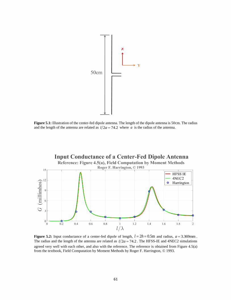
61
Figure 5.1: Illustration of the center-fed dipole antenna. The length of the dipole antenna is 50cm. The radius
and the length of the antenna are related as 2 74.2l a where a is the radius of the antenna.
Figure 5.2: Input conductance of a center-fed dipole of length, 2 0.5ml h and radius, 3.369mma .
The radius and the length of the antenna are related as 2 74.2l a . The HFSS-IE and 4NEC2 simulations
agreed very well with each other, and also with the reference. The reference is obtained from Figure 4.5(a)
from the textbook, Field Computation by Moment Methods by Roger F. Harrington, © 1993.
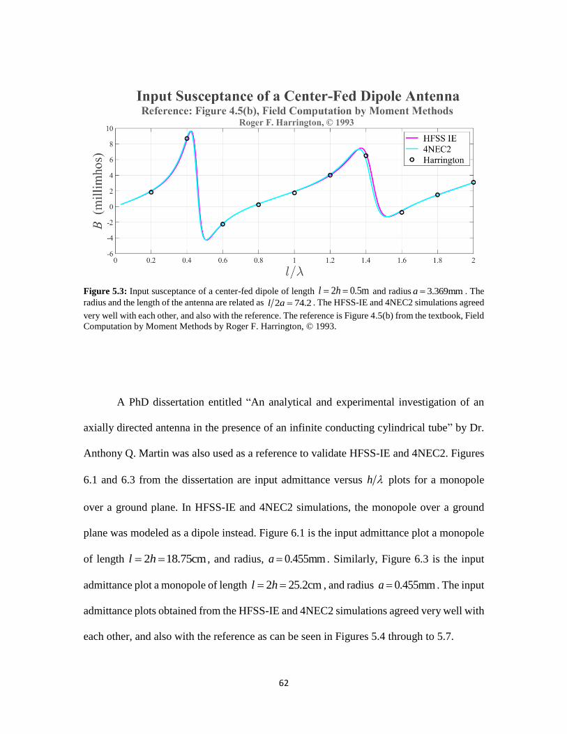
62
Figure 5.3: Input susceptance of a center-fed dipole of length 2 0.5ml h and radius 3.369mma . The
radius and the length of the antenna are related as 2 74.2l a . The HFSS-IE and 4NEC2 simulations agreed
very well with each other, and also with the reference. The reference is Figure 4.5(b) from the textbook, Field
Computation by Moment Methods by Roger F. Harrington, © 1993.
A PhD dissertation entitled “An analytical and experimental investigation of an
axially directed antenna in the presence of an infinite conducting cylindrical tube” by Dr.
Anthony Q. Martin was also used as a reference to validate HFSS-IE and 4NEC2. Figures
6.1 and 6.3 from the dissertation are input admittance versus h plots for a monopole
over a ground plane. In HFSS-IE and 4NEC2 simulations, the monopole over a ground
plane was modeled as a dipole instead. Figure 6.1 is the input admittance plot a monopole
of length 2 18.75cml h , and radius, 0.455mma . Similarly, Figure 6.3 is the input
admittance plot a monopole of length 2 25.2cml h , and radius 0.455mma . The input
admittance plots obtained from the HFSS-IE and 4NEC2 simulations agreed very well with
each other, and also with the reference as can be seen in Figures 5.4 through to 5.7.
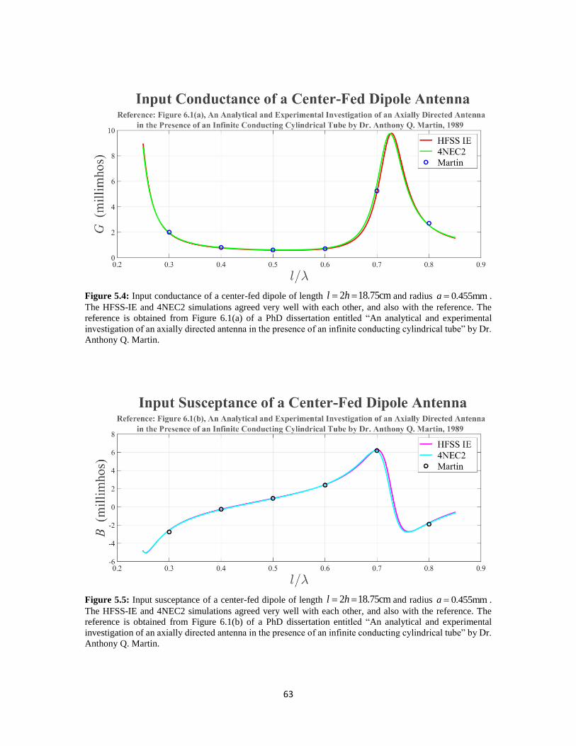
63
Figure 5.4: Input conductance of a center-fed dipole of length 2 18.75cml h and radius 0.455mma .
The HFSS-IE and 4NEC2 simulations agreed very well with each other, and also with the reference. The
reference is obtained from Figure 6.1(a) of a PhD dissertation entitled “An analytical and experimental
investigation of an axially directed antenna in the presence of an infinite conducting cylindrical tube” by Dr.
Anthony Q. Martin.
Figure 5.5: Input susceptance of a center-fed dipole of length 2 18.75cml h and radius 0.455mma .
The HFSS-IE and 4NEC2 simulations agreed very well with each other, and also with the reference. The
reference is obtained from Figure 6.1(b) of a PhD dissertation entitled “An analytical and experimental
investigation of an axially directed antenna in the presence of an infinite conducting cylindrical tube” by Dr.
Anthony Q. Martin.
64
Figure 5.6: Input conductance of a center-fed dipole of length 2 25.2cml h and radius 0.455mma .
The HFSS-IE and 4NEC2 simulations agreed very well with each other, and also with the reference. The
reference is obtained from Figure 6.3(a) of a PhD dissertation entitled “An analytical and experimental
investigation of an axially directed antenna in the presence of an infinite conducting cylindrical tube” by Dr.
Anthony Q. Martin.
Figure 5.7: Input susceptance of a center-fed dipole of length 2 25.2cml h and radius 0.455mma . The
HFSS-IE and 4NEC2 simulations agreed very well with each other, and also with the reference. The reference
is obtained from Figure 6.3(b) of a PhD dissertation entitled “An analytical and experimental investigation
of an axially directed antenna in the presence of an infinite conducting cylindrical tube” by Dr. Anthony Q.
Martin.

65
II. HFSS-IE VERSUS 4NEC2
An L antenna was simulated in HFSS-IE and 4NEC2. The length and the radius of
each leg of the L antenna were 50cm and 1mm, respectively. The illustration of the antenna
is shown in Figure 5.8. The antenna was fed at 2.5mm from the bottom of the leg parallel
to Z-axis. A frequency sweep was run such that 0.1GHz 1.2GHzf . The real and
imaginary parts of the input impedance were plotted as shown in Figure 5.9. Also, the far-
field gain was plotted as shown in Figure 5.10. As can be seen, the HFSS-IE and 4NEC2
simulations agreed very well with each other. Then, progressively more complicated
structures were simulated in HFSS-IE and 4NEC2, and the input impedance and far-field
gain were plotted. The illustration of these structures and the comparison of the simulation
results are shown in Figures 5.11 through 5.24. The transmission efficiency plot for a
system of coupled loops was plotted for a smaller range of frequencies, and slight
differences were seen between HFSS-IE and 4NEC2 simulations as the system was made
progressively more complicated. However, the plots showed very similar pattern. This
proves that for structures as complicated as an array model, 4NEC2, which is available for
free, works just as well as HFSS-IE, which costs a lot of money.
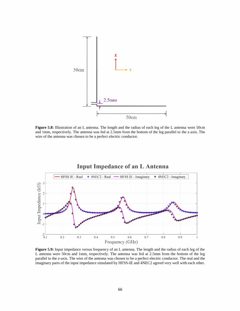
66
Figure 5.8: Illustration of an L antenna. The length and the radius of each leg of the L antenna were 50cm
and 1mm, respectively. The antenna was fed at 2.5mm from the bottom of the leg parallel to the z-axis. The
wire of the antenna was chosen to be a perfect electric conductor.
Figure 5.9: Input impedance versus frequency of an L antenna. The length and the radius of each leg of the
L antenna were 50cm and 1mm, respectively. The antenna was fed at 2.5mm from the bottom of the leg
parallel to the z-axis. The wire of the antenna was chosen to be a perfect electric conductor. The real and the
imaginary parts of the input impedance simulated by HFSS-IE and 4NEC2 agreed very well with each other.
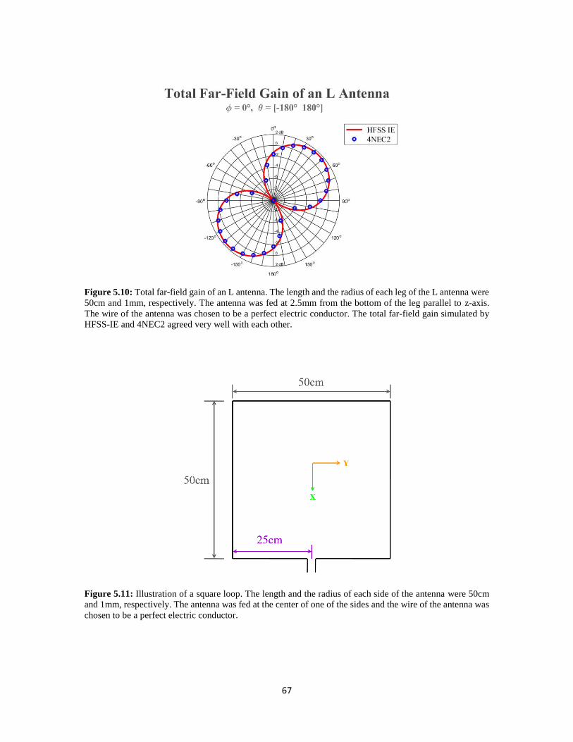
67
Figure 5.10: Total far-field gain of an L antenna. The length and the radius of each leg of the L antenna were
50cm and 1mm, respectively. The antenna was fed at 2.5mm from the bottom of the leg parallel to z-axis.
The wire of the antenna was chosen to be a perfect electric conductor. The total far-field gain simulated by
HFSS-IE and 4NEC2 agreed very well with each other.
Figure 5.11: Illustration of a square loop. The length and the radius of each side of the antenna were 50cm
and 1mm, respectively. The antenna was fed at the center of one of the sides and the wire of the antenna was
chosen to be a perfect electric conductor.
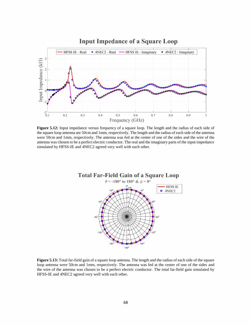
68
Figure 5.12: Input impedance versus frequency of a square loop. The length and the radius of each side of
the square loop antenna are 50cm and 1mm, respectively. The length and the radius of each side of the antenna
were 50cm and 1mm, respectively. The antenna was fed at the center of one of the sides and the wire of the
antenna was chosen to be a perfect electric conductor. The real and the imaginary parts of the input impedance
simulated by HFSS-IE and 4NEC2 agreed very well with each other.
Figure 5.13: Total far-field gain of a square loop antenna. The length and the radius of each side of the square
loop antenna were 50cm and 1mm, respectively. The antenna was fed at the center of one of the sides and
the wire of the antenna was chosen to be a perfect electric conductor. The total far-field gain simulated by
HFSS-IE and 4NEC2 agreed very well with each other.
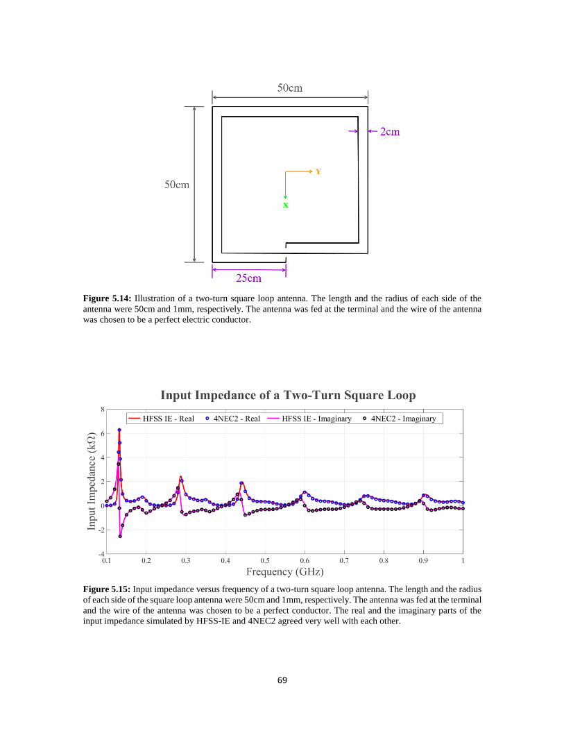
69
Figure 5.14: Illustration of a two-turn square loop antenna. The length and the radius of each side of the
antenna were 50cm and 1mm, respectively. The antenna was fed at the terminal and the wire of the antenna
was chosen to be a perfect electric conductor.
Figure 5.15: Input impedance versus frequency of a two-turn square loop antenna. The length and the radius
of each side of the square loop antenna were 50cm and 1mm, respectively. The antenna was fed at the terminal
and the wire of the antenna was chosen to be a perfect conductor. The real and the imaginary parts of the
input impedance simulated by HFSS-IE and 4NEC2 agreed very well with each other.
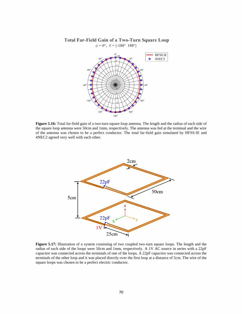
70
Figure 5.16: Total far-field gain of a two-turn square loop antenna. The length and the radius of each side of
the square loop antenna were 50cm and 1mm, respectively. The antenna was fed at the terminal and the wire
of the antenna was chosen to be a perfect conductor. The total far-field gain simulated by HFSS-IE and
4NEC2 agreed very well with each other.
Figure 5.17: Illustration of a system consisting of two coupled two-turn square loops. The length and the
radius of each side of the loops were 50cm and 1mm, respectively. A 1V AC source in series with a 22pF
capacitor was connected across the terminals of one of the loops. A 22pF capacitor was connected across the
terminals of the other loop and it was placed directly over the first loop at a distance of 5cm. The wire of the
square loops was chosen to be a perfect electric conductor.
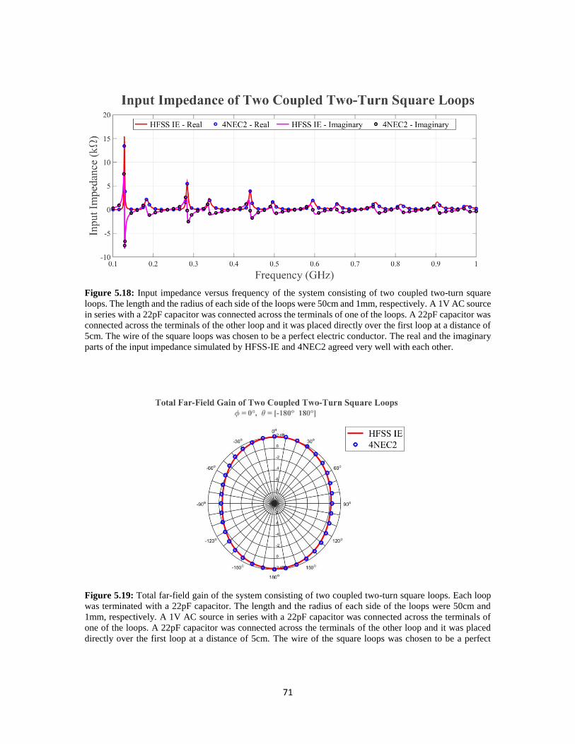
71
Figure 5.18: Input impedance versus frequency of the system consisting of two coupled two-turn square
loops. The length and the radius of each side of the loops were 50cm and 1mm, respectively. A 1V AC source
in series with a 22pF capacitor was connected across the terminals of one of the loops. A 22pF capacitor was
connected across the terminals of the other loop and it was placed directly over the first loop at a distance of
5cm. The wire of the square loops was chosen to be a perfect electric conductor. The real and the imaginary
parts of the input impedance simulated by HFSS-IE and 4NEC2 agreed very well with each other.
Figure 5.19: Total far-field gain of the system consisting of two coupled two-turn square loops. Each loop
was terminated with a 22pF capacitor. The length and the radius of each side of the loops were 50cm and
1mm, respectively. A 1V AC source in series with a 22pF capacitor was connected across the terminals of
one of the loops. A 22pF capacitor was connected across the terminals of the other loop and it was placed
directly over the first loop at a distance of 5cm. The wire of the square loops was chosen to be a perfect
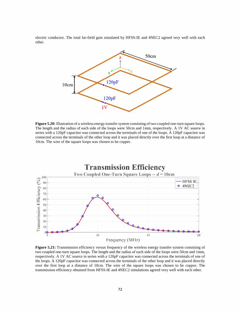
72
electric conductor. The total far-field gain simulated by HFSS-IE and 4NEC2 agreed very well with each
other.
Figure 5.20: Illustration of a wireless energy transfer system consisting of two coupled one-turn square loops.
The length and the radius of each side of the loops were 50cm and 1mm, respectively. A 1V AC source in
series with a 120pF capacitor was connected across the terminals of one of the loops. A 120pF capacitor was
connected across the terminals of the other loop and it was placed directly over the first loop at a distance of
10cm. The wire of the square loops was chosen to be copper.
Figure 5.21: Transmission efficiency versus frequency of the wireless energy transfer system consisting of
two coupled one-turn square loops. The length and the radius of each side of the loops were 50cm and 1mm,
respectively. A 1V AC source in series with a 120pF capacitor was connected across the terminals of one of
the loops. A 120pF capacitor was connected across the terminals of the other loop and it was placed directly
over the first loop at a distance of 10cm. The wire of the square loops was chosen to be copper. The
transmission efficiency obtained from HFSS-IE and 4NEC2 simulations agreed very well with each other.
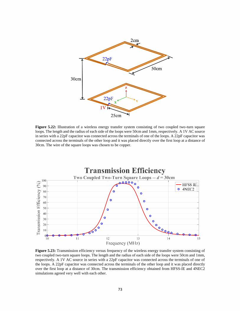
73
Figure 5.22: Illustration of a wireless energy transfer system consisting of two coupled two-turn square
loops. The length and the radius of each side of the loops were 50cm and 1mm, respectively. A 1V AC source
in series with a 22pF capacitor was connected across the terminals of one of the loops. A 22pF capacitor was
connected across the terminals of the other loop and it was placed directly over the first loop at a distance of
30cm. The wire of the square loops was chosen to be copper.
Figure 5.23: Transmission efficiency versus frequency of the wireless energy transfer system consisting of
two coupled two-turn square loops. The length and the radius of each side of the loops were 50cm and 1mm,
respectively. A 1V AC source in series with a 22pF capacitor was connected across the terminals of one of
the loops. A 22pF capacitor was connected across the terminals of the other loop and it was placed directly
over the first loop at a distance of 30cm. The transmission efficiency obtained from HFSS-IE and 4NEC2
simulations agreed very well with each other.
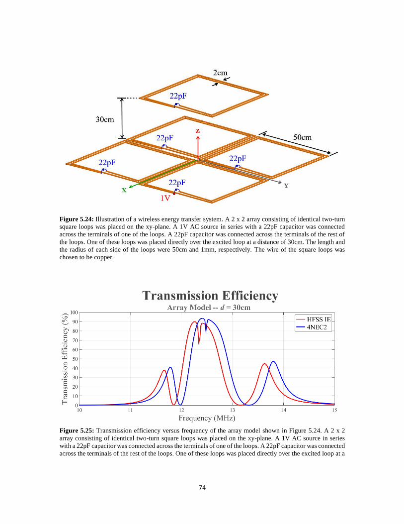
74
Figure 5.24: Illustration of a wireless energy transfer system. A 2 x 2 array consisting of identical two-turn
square loops was placed on the xy-plane. A 1V AC source in series with a 22pF capacitor was connected
across the terminals of one of the loops. A 22pF capacitor was connected across the terminals of the rest of
the loops. One of these loops was placed directly over the excited loop at a distance of 30cm. The length and
the radius of each side of the loops were 50cm and 1mm, respectively. The wire of the square loops was
chosen to be copper.
Figure 5.25: Transmission efficiency versus frequency of the array model shown in Figure 5.24. A 2 x 2
array consisting of identical two-turn square loops was placed on the xy-plane. A 1V AC source in series
with a 22pF capacitor was connected across the terminals of one of the loops. A 22pF capacitor was connected
across the terminals of the rest of the loops. One of these loops was placed directly over the excited loop at a

75
distance of 30cm. The length and the radius of each side of the loops were 50cm and 1mm, respectively. The
wire of the square loops was chosen to be copper. The transmission efficiency plot obtained from HFSS-IE
and 4NEC2 simulations had similar trend but there was some frequency shift.

76
CONCLUSIONS
A medium-range wireless energy transfer system for electric vehicle application
was designed using two loosely coupled conducting loops, each terminated with a
capacitor. The system was studied as an equivalent circuit consisting of two coupled series
RLC circuits. The resonant frequency of any RLC circuit is determined by its total
inductance, L and total capacitance, C . The energy coupled from one circuit to the other
in a loosely coupled system is the maximum when the resonant frequencies of the circuits
are the same. The transmission efficiency of the wireless energy transfer system over the
frequency range 8 MHz to 15 MHz was simulated using software tools: HFSS-IE and
4NEC2. In HFSS-IE, 21S is computed as part of the solution, whereas, in 4NEC2, it is not.
In Section III of Chapter 2, the method of obtaining scattering parameters from 4NEC2
simulation was discussed.
Two models of the wireless energy transfer system were identified: basic and array.
The basic model consisted of two loosely coupled two-turn square loops. The array model
consisted of a 2 x 2 array of a transmitter, and three parasites, and a coupled receiver. The
wireless energy transfer systems were built and the scattering parameter measurements
were taken using a network analyzer. . The scattering parameter measurement of the basic
model was taken with the receiver at various heights from the transmitter, and as the
transmitter and the receiver were brought closer together, double humps were seen in the

77
transmission efficiency versus frequency plots as was shown in Section II of Chapter 2. In
theory, the winding direction of the loops has no effect on the transmission efficiency of
the system. This was not true for the experiment and it was shown that the differences were
caused most likely by the cables connecting the loops to the network analyzer. HFSS-IE
and 4NEC2 simulations were performed with the cables included in the model, and as a
result, the transmission efficiency differed for the clockwise and the counterclockwise
wound receiver. Also, the reproducibility of the experiment was confirmed by comparing
the results of the basic model with the loops built on styrofoam and cardboard substrates.
Since the wireless energy transfer system was designed for electric vehicle charging
application, it is important to realize that without any parking assistance in place, the
transmitter and the receiver alignment depends on the skill of any given driver. This could
have a negative impact on the transmission efficiency as a result of which charge times
would increase. Hence, the receiver was intentionally misaligned 10cm in the x- and y-
directions, simultaneously. The misalignment resulted in a drop in the transmission
efficiency. The array model was designed as a remedy to the misalignment problems the
basic model is susceptible to.
The array model experiment was performed with the receiver placed at five
different locations on the xy-plane at a fixed height from the 2 x 2 array of the transmitter
and the parasites with the array on the xy-plane. The transmission efficiency at the resonant
frequency varied with the receiver location; however, the transmission efficiency was the
least sensitive to the receiver location at a different frequency. Hence, the receiver was

78
tuned to resonate at this frequency which improved the transmission efficiency. However,
the basic model with the receiver properly aligned and also the transmitter and the receiver
wound in opposite directions resulted in a much higher transmission efficiency (92%)
compared to the array model (36% - 60%). A basic model with parking assistance would
guarantee transmission efficiency >90% at all times, however an array model can only
guarantee at least 36%.
Future work should address ways to avoid the impact of the cables on the
experiment. The transmission efficiency of the array model needs to be improved. Using
excited loops instead of the parasites could possibly improve the transmission efficiency.
Other future works include developing a shielding enclosure for the system, and designing
the necessary circuitry to feed the transmitter and also to charge the battery of an electric
vehicle.

79
REFERENCES
[1] N. Tesla, “Apparatus for Transmitting Electrical Energy,” U.S. Patent 1,119,732,
issued in December 1914.
[2] T. Kelly, “The Tesla Genius,” Arizona Journal of Natural Philosophy, vol. 1, no. 7,
pp. 3-10, 1987.
[3] https://www.wirelesspowerconsortium.com/
[4] T. Hubing, Grounding and Shielding.
[5] A. Kurs, A. Karalis, R. Moffatt, J. D. Joannopoulos, P. Fisher, and M. Soljacic,
“Wireless power transfer via strongly coupled magnetic resonances,” Science, vol.
317, pp. 83-86, Jul 6 2007.
[6] ANSYS®, Release 15.0, hfss_onlinehelp, ANSYS Inc.
[7] A. Voors, NEC-2 Manual, Part III: User’s Guide, 1996.
[8] B. Dibner, Oersted and the discovery of electromagnetism, Norwalk, Connecticut:
Burndy Library, 1961.
[9] C. Paul, Inductance: Loop and Partial, Hoboken, N.J.: Wiley, IEEE, c2010.
[10] B. Dibner, “Ten Founding Fathers of the Electrical Science: V. Andre Marie
Ampere: and the Beginning of Electrodynamics,” Electrical Engineering 73, Issue
8, pp. 724-725, Aug 1954.
[11] C. Cooper, “The Truth about Tesla: The Myth of the Lone Genius in the History of
Innovation,” Library Journal 140, Issue 20, p.125, Dec 2015.
[12] B. Dibner, “Ten Founding Fathers of the Electrical Science: VIII. Michael Faraday:
And the Discovery of Electromagnetic Induction,” Electrical Engineering 73, Issue
11, pp. 966-967, Nov 1954.
[13] M. Sadiku, Elements of Electromagnetics, 5th ed., New York, New York: Oxford
University Press, 2010.
[14] B. Dibner, “Ten Founding Fathers of the Electrical Science: IX. Joseph Henry: On
Electromagnetism and Telegraphy,” Electrical Engineering 73, Issue 12, pp. 1072-
1073, Dec 1954.

80
[15] L. Schafer, Charging Ahead: An Introduction to Electromagnetism, Arlington,
Virginia: NSTA Press, c2001.
[16] J. Al-Khalili, “The birth of the electric machines: a commentary on Faraday (1832)
‘Experimental researches in electricity’,” Phil. Trans. R. Soc. A 373: 20140208,
2015.
[17] S. Chapman, Electric Machinery Fundamentals, 4th ed. New York, New York:
McGraw-Hill Companies, Inc., 2005.
[18] T. Martin, Faraday’s Discovery of Electro-Magnetic Induction, London, United
Kingdom: Edward Arnold & Co., 1949.
[19] D. M. Pozar, Microwave Engineering, 4th ed., Oxford, United Kingdom: Wiley,
John & Sons, 2011.
[20] C. A. Balanis, Antenna Theory Analysis and Design, 3rd ed., John Wiley & Sons,
Inc., 2005.
[21] A. C. Polycarpou, Introduction to the Finite Element Method in Electromagnetics,
1st ed., Morgan and Claypool Publishers, 2006.
[22] J. Jin, The Finite Element Method in Electromagnetics, John Wiley & Sons, Inc.,
1993.
[23] F. E. Terman, Radio Engineering, McGraw-Hill Book Company, Inc., 1937.
[24] F. E. Terman, Radio Engineers’ Handbook, McGraw-Hill Book Company, Inc.,
1943.
[25] A. P. Sample, “Analysis, Experimental Results, and Range Adaptation of
Magnetically Coupled Resonators for Wireless Power Transfer,” IEEE
Transactions on Industrial Electronics, vol. 58, No. 2, Feb 2011.
[26] C. Butler, “The Equivalent Radius of a Narrow Conducting Strip,” IEEE
Transactions on Antennas and Propagation, vol. AP-30, No. 4, Jul 1982.
[27] K. Miwa, H. Mori, N. Kikuma, H. Hirayama and K. Sakakibara, “A Consideration
of Efficiency Improvement of Transmitting Coil Array in Wireless Power Transfer
with Magnetically Coupled Resonance,” 2013 IEEE Wireless Power Transfer
(WPT), Perugia, 2013, pp. 13-16.

81
[28] T. Imura, H. Okabe and Y. Hori, "Basic experimental study on helical antennas of
wireless power transfer for Electric Vehicles by using magnetic resonant
couplings," 2009 IEEE Vehicle Power and Propulsion Conference, Dearborn, MI,
2009, pp. 936-940.
[29] M. Ravenstahl, "A History of Innovation," ANSYS Advantage, Volume II, Issue 4,
pp. 20-22, 2008.
[30] A. Q. Martin, “An analytical and experimental investigation of an axially directed
antenna in the presence of an infinite conducting cylindrical tube,” Dec 1989,
Clemson University, PhD Dissertation.
[31] R. F. Harrington, Field Computation by Moment Methods, IEEE PRESS, 1993.
Related Documents