Wafer processing - I Clean room environment clean room: lled temperature (20ºC), air pressure, humidity (30%) lled airbone particulates lled vibration lled lighting INESC: 250 m 2 Class 10 and 100 clean roo 250 m 2 Class 10000 (grey area) Class 100: <100 particles(>0.5m)/ft 3

Wafer processing - I Clean room environment Semiconductor clean room: - controlled temperature (20ºC), air pressure, humidity (30%) - controlled airbone.
Dec 22, 2015
Welcome message from author
This document is posted to help you gain knowledge. Please leave a comment to let me know what you think about it! Share it to your friends and learn new things together.
Transcript

Wafer processing - IClean room environment
Semiconductor clean room:- controlled temperature (20ºC), air pressure, humidity (30%)- controlled airbone particulates- controlled vibration- controlled lighting
INESC:250 m2 Class 10 and 100 clean room250 m2 Class 10000 (grey area)
Class 100:<100 particles(>0.5m)/ft3


Wafer processing - IIresist coating
1- Vapor priming for improved resist adhesion to substrate
- Resist adhesion to Si wafers is poor- Dehydration bake to remove adsorbed water from the surface- surfactant to promote adhesion : HMDS (hexamethyldisilazane)
Vapor priming is better than spin coating with a liquid solution because lower contamination
~1 monolayer
Table II.6 – Vapor prime coating steps Step description
Conditions
Wafer dehydration and purge oxygen from the chamber
Vacuum, 10 Torr, 2 minutes N2 inlet (heated), 760 Torr, 3 min steps 3x
Priming Vacuum, 1 Torr, 3 minutes HMDS, 6 Torr, 5 minutes
Purge prime exhaust Vacuum, 4 Torr, 1 minute N2 inlet, 500 Torr, 2 minutes Vacuum, 4 Torr, 2 minutes
Return to atmosphere (backfill) N2 inlet, 3 minutes

2- Spinning resist and soft baking
Wafer processing - IIresist coating
SVG Resist coater and developer track:
Track system for spin coating of photoresist (1.2 to 2 m thick) and for development of post-exposed wafers.
(cassettes of 25 Si wafers 6 inch)
Requirements:Good control of thickness, uniformity, viscosity, particle contaminationTypical resist thickness: 0.6-2 m
Soft baking: remove solvents and stress and promote adhesion to wafer
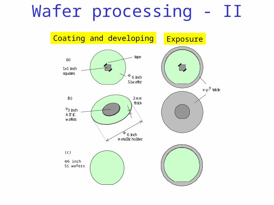
Wafer processing - II
6 inch metallic holder
2 mm thick
1x1 inch squares
3 inch AlTiC wafers
6 inch Si wafer
tape
x-y- table
(a)
(b)
Coating and developing Exposure
(c)
6 inchSi wafers

Wafer processing - IIIexposure
Heidelberg Instruments Direct Write Laser Lithography System:
Direct write lithography system utilizing a HeCd laser (=442 nm (g-line) / write lens NA= 0.85) capable of critical dimensions down to 0.8 m. System works with mask designs in GDS2 format.
INESC

Wafer processing - IVdevelopment
Positive resistsNegative resists
(INESC)
Solved in the exposed regions
Remain in the exposed regions
Selective dissolving of
resist


Resist profiles
Related Documents