1 V.S.B. ENGINEERING COLLEGE, KARUR Academic Year: 2016-2017 (EVEN Semester) Department of Electronics and Communication Engineering Course Materials (2013 Regulations) Question Bank S.No. Name of the Subject/Lab Semester Page No 1 Electronic devices II 2 2 Circuit theory II 6

Welcome message from author
This document is posted to help you gain knowledge. Please leave a comment to let me know what you think about it! Share it to your friends and learn new things together.
Transcript

1
V.S.B. ENGINEERING COLLEGE, KARUR
Academic Year: 2016-2017 (EVEN Semester)
Department of Electronics and Communication Engineering
Course Materials (2013 Regulations)
Question Bank
S.No. Name of the Subject/Lab Semester Page No
1 Electronic devices II 2
2 Circuit theory II 6

2
ELECTRONIC DEVICES
UNIT – I
SEMICONDUCTOR DIODE
PART-A
1. What is drift velocity?
2. Define drift current.
3. Define Diffusion Current
4. Define diffusion length.
5. What is depletion region in PN junction?
6. Give the other names of depletion region?
7. What is barrier potential?
8. What are the types of biasing a PN junction?
9. What is forward bias and reverse bias in a PN junction?
10. What is reverse bias in a PN junction?
11. Why contact differences of potential exist in PN junction?
12. What is the static resistance of a diode?
13. Define dynamic resistance.
14. Define dynamic conductance.
15. Which charge carriers is majority and minority carrier in N-type Semiconductor?
16. Which charge carriers is majority and minority carrier in P-type Semiconductor?
17. What is mobility? What is its unit?
18. Define Conductivity.
19. Give the relationship between mobility and conductivity.
20. Give the expression for drift current density due to electron.
UNIT II
BIPOLAR JUNCTION
1. What is transistor?
2. What are the types of transistor?
3. What is biasing?
4. What are the types of transistor configuration?
5. What is CB configuration?
6. What is CE configuration?
7. What is CC configuration?
8. What is early effect?
9. What is another name for early effect?
10. What is meant by punch through?
11. Write the current amplification factor for a CB configuration.
12. Write the formula for input resistance in a CB transistor.
13. Define output characteristics for CB configuration.
14. Write the current amplification factor for a CE transistor.
15. Write the current amplification factor for a CC transistor.
16. Write the relationship between α and β
17. Compare transistor configurations.
18. Define hybrid parameters.
19. What is the use of h - Parameters?

3
UNIT 3
FIELD EFFECT TRANSISTOR
1. Why do you call FET as field effect transistor?
2. What is a FET?
3. Why FET is called a unipolar device?
4. Define drain resistance?
5. Define pinch-off voltage
6. Mention the applications of FET.
7. What is meant by gate source threshold voltage of a FET?
8. Why FET is called voltage controlled device?
9. What are the operating regions of a JFET?
10. Give the drain current equation of JFET.
11. What are the advantages of FET
12. What is JFET?
13. What are the types of JFET?
14. Draw the symbol of JFET.
15. What are the two important characteristics of JFET?
16. What are the two modes of MOSFET?
17. Mention the operating modes of MOSFET.
18. What are the differences between JFET and MOSFET?
19. Comparison of n-channel MOSFET and p-channel MOSFET
UNIT 4
SPECIAL SEMICONDUCTOR DEVICES
1. What is MESFET?
2. What is a schottky diode?
3. Give the symbol and structure of schottky diode.
4. Give the equivalent circuit of schottky diode.
5. Give the applications of schottky diode.
6. Define Zener diode?
7. Define zener breakdown voltage.
8. List the uses of zener diode.
9. What is a varactor diode?
10. What is the significance of varactor diode ?
11. What is the applications of varactor diode?
12. What is a tunnel diode?
13. What is tunneling phenomenon?
14. Define Negative resistance of tunnel diode .
15. Define Tunneling phenomenon. (or) How does tunnel diode works ?
16. Explain the advantages of tunnel diode?
17. Explain the disadvantages of tunnel diode?
18. Explain the applications of tunnel diode?
19. Define injection laser diode
20. What are the application of LASCR?
21. what is laser?

4
UNIT 5
POWER DEVICES AND DISPLAY DEVICES
1. What is a thyristor?
2. What are the types of thyristors?
3. Give the various triggering devices for thyristors.
4. What are the regions in the VI characteristics of UJT?
5. Mention the applications of UJT.
6. What is SCR?
7. Why germanium instead of silicon is used for construction of SCR?
8. Write an two different characteristics of SCR ?
9. Mention the applications of SCR.
10. Define breakdown voltage of SCR.
11. What are the advantage of SCR?
12. What is DIAC ?
13. List out the applications of DIAC.
14. A triac is considered as two SCRs connected in reverse parallel.Why?
15. What is TRIAC ?
16. Give the symbol and structure of TRIAC.
17. Give the application of TRIAC.
18. What are the different operating modes of
TRIAC?
19. Give the VI characteristics of TRIAC
20. What is mean by solar cell ?
21. What is Photo voltaic effect?
22. What is known as photo conductive effect?
23. What is an LCD ?
24. On what factor does the color of the light emitted by a LED depend ?
25. Explain the Advantages of LED ?
26. Explain the Disadvantages of LED ?
27. Write an application of LED?
28. What is photo diode?
29. What is photo transistor?
PART-B
UNIT I
SEMICONDUCTOR DIODE
1. Explain the construction and operation of PN junction diode.
2. Derive the Current equations for PN junction diode.
3. Explain Diffusion and drift current densities.
4. Explain with neat diagram the forward and reverse bias characteristics of PN
junction diode.
5. With neat diagram explain the Switching Characteristics of PN junction diode.
UNIT II
BIPOLAR JUNCTION
1. Explain the operation of NPN and PNP transistors.
2. Define Early effect and derive the Current equations for transistors.
3. Explain the Input and Output characteristics of CE Configuration.

5
4. Explain the Input and Output characteristics of CB Configuration.
5. Explain the Input and Output characteristics of CC Configuration.
6. Describe the Hybrid -π model of Transistor.
7. Derive the h-parameter model of Transistor.
8. Explain and derive the Ebers Moll model.
9. Describe the Gummel Poon-model.
10. Explain the Multi Emitter Transistor.
UNIT III
FIELD EFFECT TRANSISTORS
1. Explain the construction and operation of JFETs
2. Sketch the Drain and Transfer characteristics of JFET and explain it.
3. Derive the Current equations of JFET and explain Pinch off voltage and its
significance.
4. Explain the construction and operation of MOSFET.
5. Explain the Characteristics of MOSFET.
6. Explain the construction and operation of D-MOSFET and E-MOSFET.
7. Derive the Current equation for MOSFET.
8. Explain the construction and operation of FINFET.
9. Explain the construction and operation of DUAL GATE MOSFET.
UNIT IV
SPECIAL SEMICONDUCTOR DEVICES
1. Explain the construction and operation of MESFET
2. Explain the construction and operation of Schottky barrier diode
3. Explain the construction and operation of Zener diode
4. Explain the construction and operation of Varactor diode
5. Explain the construction and operation of Tunnel diode
6. Explain the construction and operation of any two Gallium Arsenide device.
UNIT V
POWER DEVICES AND DISPLAY DEVICES
1. Explain the construction and operation of UJT
2. Explain the construction and operation of SCR
3. Explain the construction and operation of Diac
4. Explain the construction and operation of Triac
5. Explain the construction and operation of Power BJT
6. Explain the construction and operation of Power MOSFET and explain its types
in detail.
7. Explain the construction and operation of LED
8. Explain the construction and operation of LCD
9. Explain the construction and operation of Photo transistor
10. Explain the construction and operation of Opto Coupler
11. Explain the construction and operation of Solar cell
12. Explain the construction and operation of CCD.

6
CIRCUIT THEORY
UNIT I
PART-A
1. What is a graph of network?
2. What is tree of a network?
3. Give the properties of tree in a graph.
4. Define Ohms Law.
5. Define Quality factor.
6. What are half power frequencies?
7. Define selectivity.
8. Write the characteristics of series resonance.
9. What is anti resonance?
10. Write the characteristics of parallel resonance.
11. Define KCL
12. Define KVL
13. What is meant by linear and nonlinear elements?
14. What is meant by active and passive elements?
15. What is meant by unilateral and bilateral elements?
16. What is a dual network?
17. Give the steps to draw a Dual Network
18. Mention the disadvantages of Ohm’s Law.
19. Compare series and parallel circuit
20. What is a node?
21. What are the classifications of Circuit elements?
22. What are dependent and independent sources?
23. Define series and parallel connection.
24. What is a super node?
25. What is principle node?
26. What is a closed path?
27. State voltage division rule.
28. State current division rule.
29. Define mesh.
30. What is a planar circuit?
31. Define super mesh.
UNIT-II
PART-A
1. Sate superposition theorem.
2. State Thevenins theorem
3. State Norton’s theorem
4. State maximum power transfer theorem.
5. State reciprocity theorem.
6. State compensation theorem.
7. State Millman’s theorem.
8. State Tellegen’s theorem.
9. State the steps to solve the super position theorem.
7
10. State the steps to solve the Thevenin’s theorem.
11. State the steps to solve the Norton’s theorem.
12. What is the Load current in a Norton’s circuit?
13. What is the load current in Thevenin’s circuit?
14. What is the maximum power in a circuit?
15. Write some applications of maximum power transfer theorem.
16. What is the limitation of superposition theorem?
17. What are the limitations of maximum power transfer theorem?
18. State voltgae division rule.
19. State current division rule.
20. Define source transformtion.
21. List the applications of Thevinins theorem.
22. Explain the purpose of star delta transformation.
UNIT-III
PART-A
1. What is meant by Resonance?
2. Write the expression for the resonant frequency of a RLC series circuit.
3. What is resonant frequency?
4. Define series resonance.
5. Define Quality factor.
6. What are half power frequencies?
7. Define selectivity.
8. Write the characteristics of series resonance.
9. What is anti resonance?
10. Write the characteristics of parallel resonance.
18. What is Bandwidth and selectivity?
19. What are coupled circuits?
20. What are coupled circuits?
21. State the properties of a series RLC circuit.
22. State the properties of a parallel RLC circuit.
23. Define self inductance.
24. Define mutual inductance.
25. Define coefficient of coupling.
26. What is DOT convention?
27. State dot rule for coupled circuit.
28. Define coefficient of coupling.
UNIT-IV
PART-A
1. What is transient state?
2. What is transient time?
3. What is transient response?
4. Define time constant of RLC circuit.
5. Define time constant of RC circuit.
6. What is meant by natural frequency?
7. Define damping ratio.

8
8. Write down the condition, for the response of RLC series circuit to be under damped
for step input.
9. Write down the condition for the response of RLC sereis circuit to be over damped for
step input.
10. Write down the few applications of RL, RC, RLC circuits.
11. Define transient response.
12. What is natural response?
13. What is forced response?
14. Define apparent power.
15. What is power factor and reactive power?
UNIT-V
PART-A
1. Define line current and phase current.
2. Define line and phase voltgae
3. Give the line and phase values in star connection
4. Give the line and phase values in delta connection
5. Write few methods available for measuring in 3-phase load.
6. List the methods used for power measurement with single wattmeter
7. List the methods for unbalanced star connected load
8. Write the methods of connectios of 3 phase windings?
PART B
UNIT I
1. Find the current through each branch by network reduction technique.
2. Calculate a) the equivalent resistances across the terminals of the supply, b) total
current
supplied by the source and c) power delivered to 16 ohm resistor in the circuit shown in
figure.
3. In the circuit shown, determine the current through the 2 ohm resistor and the total

9
current delivered by the battery. Use Kirchhoff’s laws.
4. (i) Determine the current through 800 ohm resistor in the network shown in figure.
(ii) Find the power dissipated in 10 ohm resistor for the circuit shown in figure.
5. (i) In the network shown below, find the current delivered by the battery.
(ii) Discuss about voltage and current division principles.

10
6. (i) Explain :
a) Kirchoff laws. (4)
b) Dependent sources (2)
c) Source transformations (2)
d) With relevant diagrams Voltage division and current division rule (4)
(ii) Calculate the resistance between the terminals A – B.
7. i)Determine the value of V2 such that the current through the impedance (3+j4) ohm is
Zero
ii) Find the current through branch a-b using mesh analysis shown in figure below.
8. Determine the mesh currents I1 and I2 for the given circuit shown below
9. Find the node voltages V1 and V2 and also the current supplied by the source for the
circuit shown below.

11
10. Find the nodal voltages in the circuit of figure.
11. i) Using the node voltage analysis, find all the node voltages and currents in 1/3 ohm
and 1/5
ohm resistances of figure.
ii) For the mesh-current analysis, explain the rules for constructing mesh impedance
matrix and solving the matrix equation [Z]I = V.
12. Solve for V1 and V2 using nodal method. Let V = 100V.
13. Using Mesh analysis, find current through 4 ohm resistor.

12
14. Use nodal voltage method to find the voltages of nodes ‘m’ and ‘n’ and currents
through j2 ohm and –j2 ohm reactance in the network shown below.
15. For the circuit shown find the current I flowing through 2 ohm resistance using loop
analysis.
UNIT II
1. (i) Find the value of R and the current flowing through it in the circuit shown when the
current
in the branch OA is zero.
ii) Determine the Thevenin’s equivalent for the figure
13
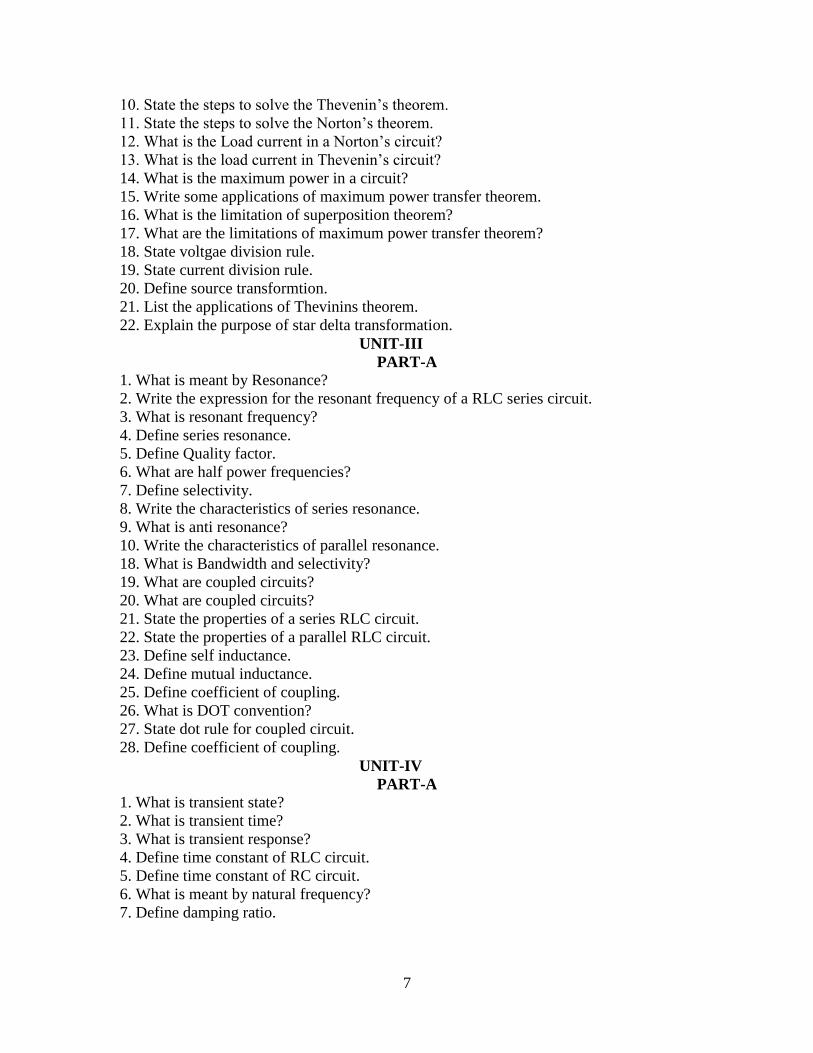
2. Derive expressions for star connected arms in terms of delta connected arms and delta
connected arms in terms of star connected arms.
3. Determine Thevenin’s equivalent across the terminals AB for the circuit shown in
figure below.
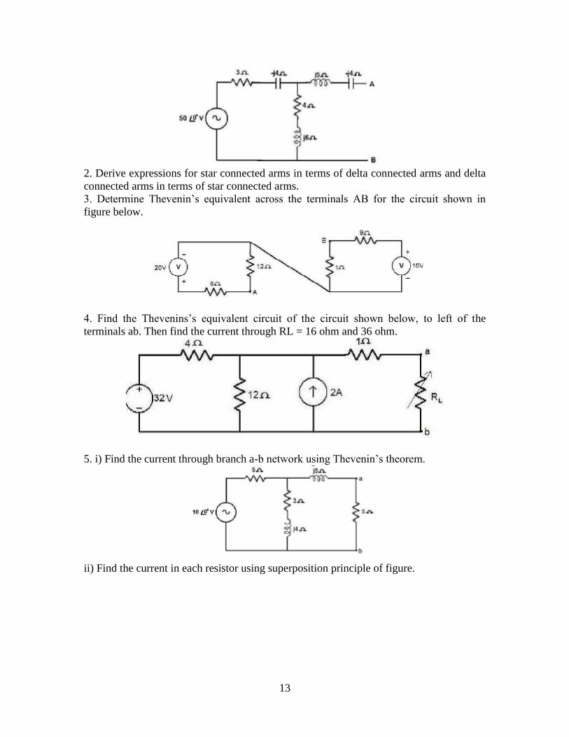
4. Find the Thevenins’s equivalent circuit of the circuit shown below, to left of the
terminals ab. Then find the current through RL = 16 ohm and 36 ohm.
5. i) Find the current through branch a-b network using Thevenin’s theorem.
ii) Find the current in each resistor using superposition principle of figure.

14
6. i) Determine the Thevenin’s equivalent circuit.
ii) Determine the equivalent resistance across AB of the circuit shown in the figure
below.
7. For the circuit shown, use superposition theorem to compute current I.
8. (i)Compute the current in 23 ohm resistor using super position theorem for the circuit
shown below.

15
(ii) Find the equivalent resistance between B and C in figure
9. Using superposition theorem calculate current through (2+j3) ohm impedance branch
of the
circuit shown.
10. i) For the circuit shown, determine the current in (2+j3) ohm by using superposition
theorem.
ii) State and prove Norton’s theorem.
11.i) Find the value of RL so that maximum power is delivered to the load resistance
shown in figure.
16
ii) State and prove compensation theorem.
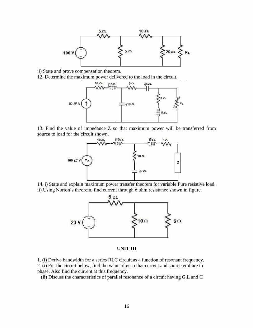
12. Determine the maximum power delivered to the load in the circuit.
13. Find the value of impedance Z so that maximum power will be transferred from
source to load for the circuit shown.
14. i) State and explain maximum power transfer theorem for variable Pure resistive load.
ii) Using Norton’s theorem, find current through 6 ohm resistance shown in figure.
UNIT III
1. (i) Derive bandwidth for a series RLC circuit as a function of resonant frequency.
2. (i) For the circuit below, find the value of ω so that current and source emf are in
phase. Also find the current at this frequency.
(ii) Discuss the characteristics of parallel resonance of a circuit having G,L and C
17
3. (i) A Pure resistor, a pure capacitor and a pure inductor are connected in parallel across
a50Hz supply, find the impedance of the circuit as seen by the supply. Also find the
resonantfrequency.
(ii) When connected to a 230V, 50Hz single phase supply, a coil takes 10kVA and
8kVAR. Forthis coil calculate resistance, inductance of coil and power consumed.
4. (i) In an RLC series circuit if ω1 and ω2 are two frequencies at which the magnitude of
thecurrent is the same and if ωr is the resonant frequency, prove that ω2 r = ω1ω2.
(ii) A series RLC circuit has Q = 75 and a pass band (between half power frequencies) of
160Hz. Calculate the resonant frequency and the upper and lower frequencies of the pass
band.
5. (i) Explain and derive the relationships for bandwidth and half power frequencies of
RLCseries circuit. (ii) Determine the quality facto of a coil R = 10 ohm, L = 0.1H and C
= 10Μf
6. A series RLC circuit has R=20 ohm, L=0.005H and C = 0.2 x 10⁻⁶ F. It is fed from a
100Vvariable frequency source. Find i) frequency at which current is maximum ii)
impedance at thisfrequency and iii) voltage across inductance at this frequency.
7. A series RLC circuit consists of R=100 ohm, L = 0.02 H and C = 0.02 microfarad.
Calculatefrequency of resonance. A variable frequency sinusoidal voltage of constant
RMS value of 50Vis applied to the circuit. Find the frequency at which voltage across L
and C is maximum. Alsocalculate voltage across L and C is maximum. Also calculate
voltages across L and C atfrequency of resonance. Find maximum current in the circuit.
8. In the parallel RLC circuit, calculate resonant frequency, bandwidth, Q-factor and
power dissipated at half power frequencies.
UNIT IV
1. A resistance R and 2 microfarad capacitor are connected in series across a 200V direct
supply.Across the capacitor is a neon lamp that strikes at 120V. Calculate R to make the
lamp strike 5sec after the switch has been closed. If R = 5Megohm, how long will it take
the lamp to strike?
2. A Series RLC circuits has R=50 ohm, L= 0.2H, and C = 50 microfarad. Constant
voltage of100V is impressed upon the circuit at t=0. Find the expression for the transient
current assuminginitially relaxed conditions.
3. A Series RLC circuits with R=300 ohm, L=1H and C=100x10-6 F has a constant
voltage of50V applied to it at t= 0. Find the maximum value of current ( Assume zero
initial conditions)
4.A step voltage V(t) = 100 u(t) is applied to a series RLC circuit with L=10H, R=2ohm
and C=5F. The initial current in the circuit is zero but there is an initial voltage of 50V on
the capacitorin a direction which opposes the applied source. Find the expression for the
current in the circuit.
5. For a source free RLC series circuit, the initial voltage across C is 10V and the initial
currentthrough L is zero. If L = 20mH, C=0.5 microfarad and R=100 ohm. Evaluate i(t).
UNIT V
1. With a neat circuit and phasor diagram explain the three phase power measurement by
twowattmeter method.

18
2. (i) A symmetrical three phase 400V system supplies a balanced delta connected load.
Thecurrent in each branch circuit is 20A and phase angle 40° (lag) calculate the line
current and totalpower.
(ii) A three phase delta connected load has Zab = (100+j0) ohms, Zbc = (-j100) ohms and
Zca =(70.7 =j70.7) ohms is connected to a balanced 3 phase 400V supply. Determine the
line currentsIa,Ib and Ic. Assume the phase sequence abc.
3. (i) A balanced three phase star connected load with impedance 8+j6 ohm per phase is
connected across a symmetrical 400V three phase 50Hz supply. Determine the line
current,power factor of the load and total power.
(ii) An alternating current is expressed as i=14.14 sin 314t. Determine rms current,
frequencyand instantaneous current hen t =0.02ms.
4. (i) A balanced star connected load of 4+j3 ohm per phase is connected to a 400V, 3
phase,50Hz supply. Find the line current, power factor, power, reactive volt ampere and
total voltampere.
(ii) A Voltage source 100V with resistance of 10 ohms and inductance 50 mH, a
capacitor 50microfarad are connected in series. Calculate the impedance when the
frequency is (i) 50HZ (ii)500Hz (iii) the power factor at 100Hz.
5. (i) Three impedances Z1 = 3∟45° ohm, Z2 = 10√2∟45° ohm, Z3 = 5∟-90° ohm are
connected in series. Calculate applied voltage if voltage across Z1 = 27∟-10° V.
(ii) A delta connected load as shown in figure is connected across 3 phase 100 volt
supply.Determine all line currents.
Related Documents