http://www.ieee-tcvlsi.org VLSI Circuits and Systems Letter Volume 2, Issue 2, October 2016 Editorial Features • Jingtong Hu, Yongpan Liu and Chun Jason Xue, Non-Volatile Processor: Circuit, System, and Software • Qi Zhu, Cross-Layer Modeling, Exploration and Validation for Connected Vehicles • Shamza Sheikh, S. K. Vishvakarma and B.S. Reniwal, An Offset Compensated Sense Amplifier Based On Charge Storage Technique for SRAM Opinions • Anirban Sengupta, Mathematical Models for Latency Estimation of Loop Unrolled and Loop Pipelined CDFGS during High Level Synthesis Updates • Upcoming conferences and workshops • Awards Outreach and Community Call for Contributions

Welcome message from author
This document is posted to help you gain knowledge. Please leave a comment to let me know what you think about it! Share it to your friends and learn new things together.
Transcript

http://www.ieee-tcvlsi.org
VLSI Circuits and Systems Letter
Volume 2, Issue 2, October 2016
Editorial
Features • Jingtong Hu, Yongpan Liu and Chun Jason Xue, Non-Volatile Processor: Circuit, System, and Software • Qi Zhu, Cross-Layer Modeling, Exploration and Validation for Connected Vehicles • Shamza Sheikh, S. K. Vishvakarma and B.S. Reniwal, An Offset Compensated Sense Amplifier Based On Charge
Storage Technique for SRAM
Opinions • Anirban Sengupta, Mathematical Models for Latency Estimation of Loop Unrolled and Loop Pipelined CDFGS
during High Level Synthesis
Updates • Upcoming conferences and workshops • Awards
Outreach and Community
Call for Contributions

1
VLSI Circuits and Systems Letter Volume 2 – Issue 2 October 2016
Editorial
The continuous scaling of integrated circuit (IC) technologies has been driving the semiconductor industry for several decades. Nowadays, even though the scaling of mainstream CMOS technologies is starting to slow down, the field of VLSI circuits and systems continues its remarkable growth with numerous opportunities along two complementary avenues: (1) development of post-silicon devices, circuits and systems (e.g., carbon nanotube, graphene, memristor, etc.), and (2) discovery of emerging application domains (e.g., biomedical electronics, internet of things, etc.). The VLSI Circuits and Systems Letter, published twice a year, aims to report recent advances in VLSI technology, education and opportunities, and consequently, grow the research and education activities in the area.
This letter is affiliated with the Technical Committee on VLSI (TCVLSI) under the IEEE Computer Society. TCVLSI covers the design methodologies for advanced VLSI circuit and systems, including digital circuits and systems, analog and radio-frequency circuits, as well as mixed-signal circuits and systems. The emphasis of TCVLSI falls on integrating the design, computer-aided design, fabrication, application, and business aspects of VLSI while encompassing both hardware and software.
TCVLSI sponsors a number of premium conferences and workshops, including, but not limited to, ARITH, ASAP, ASYNC, iNIS, ISVLSI, IWLS, and SLIP. Emerging research topics and state-of-the-art advances on VLSI circuits and systems are reported at these events on a regular basis. Best paper awards are selected at these conferences to promote the high-quality research work each year. In addition to these research activities, TCVLSI also supports a variety of educational activities related to TCVLSI. Several student travel grants and best paper awards are sponsored by TCVLSI in various sponsored meeting. Funds are provided to compensate student travels to these meetings as well as attract more student participation. The organizing committees of these meetings undertake the task of selecting right candidates for these awards.
This issue of the VLSI Circuits and Systems Letter showcases the state-of-the-art developments covering several emerging areas: non-volatile computing, intelligent vehicle, nanoscale memory, high-level synthesis, etc. Professional articles are solicited from technical experts to provide an in-depth review of these areas. The articles can be found in the sections of “Features” and “Opinions”. In the section of “Updates”, upcoming conferences/workshops, funding opportunities and job openings are summarized. Finally, a dedicated section of “Outreach and Community” discusses the motivations and approaches for K-20 education.
We would like to express our great appreciation to all Associate Editors (Mike Borowczak, Prasun Ghosal, Shiyan Hu, Helen Li, Anirban Sengupta, Jawar Singh, Yiyu Shi and Qi Zhu) for their dedicated effort and strong support in organizing this letter. Prof. Jawar Singh is a new Associate Editor who recently joined the editorial board. The complete editorial board information is available at TCVLSI website (http://www.ieee-tcvlsi.org). We are very thankful to our web chair Mike Borowczak, for his professional service to make the letter publically available on the Internet. We wish to thank all authors who have contributed their professional articles to this issue. We hope that you will have an enjoyable moment when reading the letter! The call for contributions for the next issue is available at the end of this issue and we encourage you to submit articles, news, etc. to an associate editor covering that scope.
Saraju Mohanty would like to thank the TCVLSI community for re-electing him as the Chair of TCVLSI for 2nd term. He looks forward to working with you all to further serve the community.
Saraju Mohanty
Chair TCVLSI and Editor University of North Texas
Xin Li TCVLSI Editor
Carnegie Mellon University.

2
VLSI Circuits and Systems Letter Volume 2 – Issue 2 October 2016
Features
Non-Volatile Processor: Circuit, System, and Software Jingtong Hu, Yongpan Liu, Chun Jason Xue Oklahoma State University, Tsinghua University, City University of Hong Kong
1. Introduction and Motivation From smart phones to smart watches and glasses, smart electronic devices have become an integral part of our daily
life. However, this trend never stops. According to a market assessment by IHS [1], the market for wearable technology will grow to 60,000 million US dollars by 2018. The vision for wearable devices is to interweave technology into our everyday life and improve the quality of life. While the vision is promising and exciting, there are several challenges in achieving this goal. One of the imminent challenges is how to power all these small devices. For all these devices, a battery is no longer a favorable solution. First of all, it is difficult to shrink the size of battery while maintaining the required power supply. Second, closely wearing many batteries will pose safety and health concerns for users. What is more, charging all these batteries every one or two days will give users bad experiences. Therefore, researchers are actively pursuing power alternatives and trying to replace battery completely. Out of all possible solutions, energy harvesting is one of the most promising techniques to meet both the size and power requirements of wearable devices.
Energy harvesting devices generate electric energy from their surroundings using direct energy conversion techniques. Examples of power sources include kinetic, electromagnetic radiation (including light and RF), and thermal energy. The obtained energy can be used to recharge a capacitor or, in some cases, to directly power the electronics. However, there is an intrinsic drawback with harvested energy. They are all unstable. With an unstable power supply, the processor execution will be interrupted frequently. Frequent turning-off and booting-up will place an extra burden on a limited power budget. What is worse, in some cases, large tasks can never get finished since the intermediate results cannot be saved.
2. Non-Volatile Processor and System To address this problem, non-volatile processors (NVP) [2, 3, 5, 6, 10] have been proposed to enable instant on/off for
these devices. As shown in Figure 1 and 2, a non-volatile FRAM is attached to the processor’s volatile registers in NVP. Every time there is a power outage, the processor’s state will be saved to the NV FRAM, which is known as checkpointing. Then the next time the power comes back on, the processor’s state is copied back to the volatile registers and program execution resumes. In this way, we can make sure the program execution is “accumulative” and resistant to frequent power outage.
Figure 1: NV Processor Figure 2: NV Register with Ferroelectric Flip-Flop

3
VLSI Circuits and Systems Letter Volume 2 – Issue 2 October 2016
Figure 3: Energy Harvesting System
Figure 3 shows the architecture for a typical energy harvesting powered NVP based sensing system. Ambient energy such as light, kinetic, RF, thermal, or even biochemical energy, are harvested and stored in a small capacitor, which can be used to power the processor and peripheral devices.
While the NV processor has been developed, there is no software designed or optimized for this new category of processors to ensure the correctness and efficiency. All existing software is developed and compiled without considering these new challenges and features introduced by the NV processor. In order to efficiently utilize NV processors, existing system and software has to be optimized in the following aspects: • First, while most existing works are successful in achieving the continuous computing functionality, few of them
considered optimizing the checkpointing efficiency. On one hand, the energy harvested in such systems is usually limited. On the other hand, not only registers need to be checkpointed, but on-chip and off-chip memories also need to be checkpointed if they are volatile. Therefore, fast and efficient checkpointing is needed for the whole volatile memory hierarchy to ensure successful checkpointing. Meanwhile, more energy can be used for system forward progress.
• Second, while the computing status can be saved, I/O interfaces associated with peripheral sensors and communication devices are hard to checkpoint due to their time-sensitivity and atomicity. In many cases, interrupted operations need to be restarted from the beginning, which will severely affect the forward progress. Meanwhile, checkpointing for processor and I/O operations in interrupt service routines (ISRs) has to be handled properly to ensure correct execution.
• Third, when multiple tasks are running concurrently in the system, the OS scheduler and task management will also affect the forward progress upon power failure.
• Additionally, our study [8] showed that without considering the volatility across the memory hierarchy, data inconsistency might happen and lead to fatal errors.
3. Software Design and Optimizations for NVP Several works have been done to optimize the checkpoint efficiency. Zhao et al. [9] propose an optimization strategy
to reduce stack size to backup upon power failures. Motivated by the observation that the size of stack to back up varies along program execution, the authors propose to flexibly re-allocate the checkpoints to positions with less stack content to back up. Specifically, when receiving power failure signals, instead of instant backup, the program has the flexibility to execute further steps to look for a better location for backup, with the objective of minimizing the stack size to back up while guaranteeing successful backup with limited available energy.
Li et al. [4] also target optimization of stack backup from a different angle. The authors assume fixed checkpoints and propose to trim the stack space by address sharing among objects and functions with disjoint live ranges. The stack allocation and management policies are modified to achieve this goal. A heuristic graph coloring algorithm is proposed for allocation of data and function call sites, with the objective of sharing addresses among all objects and call sites to the greatest possible extent. After trimming, the content to back up in stack can be significantly reduced.
Ambient Energy Energy Harvesting and Management
Energy Storage
Peripheral Devices Nonvolatile Processor
Register File
IcacheNVPDcache
RF S ignal
Piezoelectric Thermal
Solar
Transceivers
NV Memory
Sensors
I2C
UART
SPI
IO Operations Computing Operations
Voltage Detector
Voltage Regulator
I2C
UART
SPI
Bus
Bus

4
VLSI Circuits and Systems Letter Volume 2 – Issue 2 October 2016
Xie et al. [7] explore the cache architecture in NVP and corresponding backup strategies. They analyze the volatile and non-volatile hybrid cache, where the non-volatile portion can be used either for caching data, or backing up data upon power failures. The authors propose to reserve sufficient non-volatile cache blocks to back up dirty ones, so that the cache content can be correctly resumed. Other non-volatile cache blocks are normally used for caching. Block placement and migration policies between volatile and non-volatile portions are proposed, and proactive write back policy is also designed for successful and efficient checkpointing, providing a guideline for cache management in NVP.
4. Conclusion Realizing accumulative computing on unstable harvested energy will enable a new class of self-powered sensing/
monitoring systems that can last for years and require the least maintenance effort in various non-timing critical applications. It will simplify system installation and maintenance in many areas such as health care, building monitoring and maintenance, traffic, agriculture and environment monitoring, and even crisis management. Meanwhile, it will help bridge the gap between ever-increasing electronic power needs and battery scalability and have the potential to provide a large infrastructure for opportunistic computing with great social impact. However, there all still several challenges to be answered to achieve the goal. This article presents two checkpoint efficiency optimization techniques which aim to overcome these challenges.
References:
[1] Wearable technology - market assessment. http://www.ihs.com/pdfs/Wearable-Technology-sep-2013.pdf. [2] Stephen Ducharme, Timothy J. Reece, C.M. Othon, and R. K. Rannow. Ferroelectric polymer Langmuir-blodgett films
for nonvolatile memory applications. IEEE Transactions on Device and Materials Reliability, 5(4):720–735, 2005. [3] Y. Horii, Y. Hikosaka, A. Itoh, K. Matsuura, M. Kurasawa, G. Komuro, K. Maruyama, T. Eshita, and S. Kashiwagi. 4
mbit embedded fram for high performance system on chip (soc) with large switching charge, reliable retention and high imprint resistance. In International Electron Devices Meeting, 2002. IEDM ’02., pages 539–542, 2002.
[4] Qingan Li, Mengying Zhao, Jingtong Hu, Yongpan Liu, Yanxiang He, and Chun Jason Xue. Compiler directed automatic stack trimming for efficient non-volatile processors. In Proceedings of the 52nd Annual Design Automation Conference, DAC ’15, pages 183:1–183:6, 2015.
[5] H. Nakamoto, D. Yamazaki, T. Yamamoto, H. Kurata, S. Yamada, K. Mukaida, T. Ninomiya, T. Ohkawa, S. Masui, and K. Gotoh. A passive uhf rf identification cmos tag ic using ferroelectric ram in 0.35-um technology. IEEE Journal of Solid-State Circuits, 42(1):101–110, 2007.
[6] Yiqun Wang, Yongpan Liu, Shuangchen Li, Daming Zhang, Bo Zhao, Mei-Fang Chiang, Yanxin Yan, Baiko Sai, and Huazhong Yang. A 3us wake-up time nonvolatile processor based on ferroelectric flip-flops. In Proceedings of the ESSCIRC, pages 149–152, 2012.
[7] Mimi Xie, Mengying Zhao, Hehe Li, Chen Pan, Youtao Zhang, Yongpan Liu, Chun Jason Xue, and Jingtong Hu. Checkpoint aware hybrid cache architecture for NV processor in energy harvesting powered systems. In International Conference on Hardware/Software Codesign and System Synthesis (CODES+ISSS), 2016, to appear.
[8] Mimi Xie, Mengying Zhao, Chen Pan, Jingtong Hu, Yongpan Liu, and Chun Jason Xue. Fixing the broken time machine: consistency-aware checkpointing for energy harvesting powered non-volatile processor. In Proceedings of the 52nd Annual Design Automation Conference, pages 184:1–184:6, 2015.
[9] Mengying Zhao, Qingan Li, Mimi Xie, Yongpan Liu, Jingtong Hu, and Chun Jason Xue. Software assisted non-volatile register reduction for energy harvesting based cyber-physical system. In Proceedings of the 2015 Design, Automation & Test in Europe Conference & Exhibition, DATE ’15, pages 567–572, 2015.
[10] M. Zwerg, A. Baumann, R. Kuhn, M. Arnold, R. Nerlich, M. Herzog, R. Ledwa, C. Sichert, V. Rzehak, P. Thanigai, and B.O. Eversmann. An 82ua/mhz microcontroller with embedded feram for energy-harvesting applications. In 2011 IEEE International Solid-State Circuits Conference Digest of Technical Papers (ISSCC),, pages 334–336, Feb 2011.
5
VLSI Circuits and Systems Letter Volume 2 – Issue 2 October 2016
Cross-Layer Modeling, Exploration and Validation for Connected Vehicles Qi Zhu Department of Electrical and Computer Engineering, University of California, Riverside
Abstract – Next-generation vehicles will not only precept the environment with their own sensors, but also communicate with other vehicles and surrounding infrastructures for vehicle safety and transportation efficiency. The design and validation of vehicle-to-vehicle (V2V) and vehicle-to-infrastructure (V2I) applications involve multiple layers, from vehicular communication networks down to software and hardware of individual vehicles, and concern with stringent requirements on a variety of design metrics. To cope with these challenges, we have been developing CONVINCE, a cross-layer design framework for connected vehicles. The framework includes mathematical models, synthesis and validation algorithms, and a heterogeneous simulator for modeling inter-vehicle communications and intra-vehicle software and hardware in a holistic environment. It explores and validates design options with respect to constraints and objectives on system safety, performance, security, fault tolerance, extensibility, and cost.
Design Challenges: Autonomous driving has made significant progress during the past decade. Many companies and academic institutions started testing their autonomous vehicles on roads. Typical autonomous vehicles utilize a variety of sensors (e.g., LIDAR, radar, GPS, cameras and ultrasound sensors) to percept the environment and make driving decisions at real-time. However, accidents have been reported for both test autonomous vehicles and commercialized vehicles with semi-autonomous driving applications. The design and operation of a safe, reliable and secure autonomous-driving system still face tremendous challenges, in particular under stringent resource constraints for commercial vehicles. First, modern automotive systems have become more complex than ever. From the functional perspective, there is a wide range of emerging applications including autonomous functions and Advanced Driver Assistance Systems (ADAS). From 2000 to 2010, embedded software increased from 2% to 13% of a vehicle’s total value, and the number of lines of code increased from one million to more than ten million [1]. From the architectural perspective, the number of Electronic Control Units (ECUs) in a standard car has gone from 20 to over 50 in the past decade. The traditional federated architecture, where each function is deployed to one ECU and provided as a black-box by Tier-1 supplier, is shifting to the integrated architecture, in which one function can be distributed over multiple ECUs and multiple functions can be supported by one ECU [2]. This leads to significantly more sharing and contention among software functions. Furthermore, there are a variety of objectives and metrics that need to be addressed during the design and operation of automotive systems, such as safety, performance, fault tolerance, extensibility, security and cost. Many of these metrics are heavily influenced by system timing behavior, and often lead to conflicting requirements. For instance, shorter sampling periods and end-to-end latencies of control loops usually lead to better sensing and control performance [3], but may be detrimental to schedulability, extensibility and even security (as there is less timing slack for adding strong security techniques [4]). It is important yet challenging to address these metrics in an integrated framework. The problems become even more challenging when connected environments and applications are considered. V2V and V2I communications (generalized as V2X) have been proposed to enhance driving safety and transportation efficiency as individual vehicles may suffer from blind spots and precision limitations. For instance, in the Dedicated Short Range Communication (DSRC) standard [5], Basic Safety Messages (BSMs) that contain vehicle state information (e.g., speed, acceleration and location) are exchanged among vehicles and surrounding infrastructures through wireless channels. Vehicles can estimate the position and movement of other vehicles based on the received messages and take early actions to avoid potential collisions or improve driving efficiency. However, designing a connected vehicle or a connected application faces many challenges. In particular, the timing behavior of V2X communication is usually less predicative than that of in-vehicle networks, since it is significantly affected by the physical environment. As results, it is more difficult to model and analyze the performance of a V2X network and guarantee the satisfaction of timing constraints that are extremely critical for automotive systems. Furthermore, while security has emerged as a major concern for in-vehicle architecture design [6], the open environment of V2X communications further broadens the potential attack surface. A connected vehicle application has to address security concerns while meeting other design constraints, in particular timing and resource constraints.
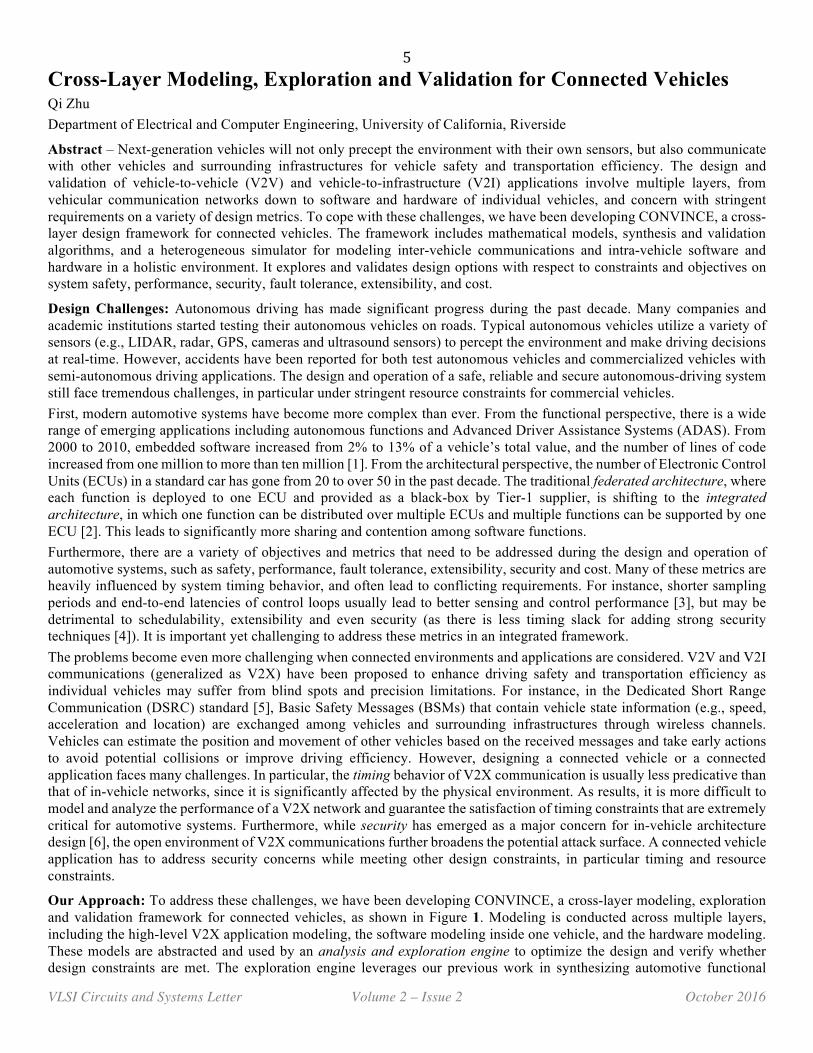
Our Approach: To address these challenges, we have been developing CONVINCE, a cross-layer modeling, exploration and validation framework for connected vehicles, as shown in Figure 1. Modeling is conducted across multiple layers, including the high-level V2X application modeling, the software modeling inside one vehicle, and the hardware modeling. These models are abstracted and used by an analysis and exploration engine to optimize the design and verify whether design constraints are met. The exploration engine leverages our previous work in synthesizing automotive functional
6
VLSI Circuits and Systems Letter Volume 2 – Issue 2 October 2016
models to software implementations, including task and message generation, allocation, scheduling with respect to a variety of design metrics [3][4][7][8][9][10]. The models are also leveraged by a simulation engine to validate system designs, identify potential issues and provide design insights.
Figure 1: CONVINCE framework for cross-layer modeling, exploration and validation of connected vehicles.
CONVINCE is still under development. We demonstrated some of the initial results through a Cooperative Adaptive Cruise Control (CACC) cases study in [11]. CACC utilizes V2V wireless communication to enhance the traditional single-vehicle adaptive cruise control by cooperatively maintaining a safe gap among vehicles. We showed that by using CONVINCE, we could analyze the impact of timing delays and security attacks in vehicular communication and ultimately CACC performance.
Reference [1] R. N. Charette. This car runs on code. IEEE Spectrum, February 2009. [2] A. Sangiovanni-Vincentelli and M. Di Natale. Embedded system design for automotive applications. Computer,
40(10):42–51, 2007. [3] P. Deng, Q. Zhu, A. Davare, A. Mourikis, X. Liu, and M. Di Natale. An efficient control-driven period optimization
algorithm for distributed real-time systems. IEEE Transactions on Computers, 2016. [4] B. Zheng, P. Deng, R. Anguluri, Q. Zhu, and F. Pasqualetti. Cross-layer codesign for secure cyber-physical systems.
IEEE Transactions on Computer-Aided Design of Integrated Circuits and Systems, 35(5):699–711, May 2016. [5] J. B. Kenney. Dedicated short-range communications (DSRC) standards in the United States. Proceedings of the IEEE,
99(7):1162–1182, 2011. [6] K. Koscher, A. Czeskis, F. Roesner, S. Patel, T. Kohno, S. Checkoway, D. McCoy, B. Kantor, D. Anderson, H.
Shacham, and S. Savage. Experimental security analysis of a modern automobile. IEEE Symposium on Security and Privacy (SP), May 2010.
[7] P. Deng, F. Cremona, Q. Zhu, M. Di Natale, and H. Zeng. A model-based synthesis flow for automotive CPS. IEEE/ACM International Conference on Cyber-Physical Systems (ICCPS), April 2015.
[8] C.-W. Lin, B. Zheng, Q. Zhu, and A. Sangiovanni-Vincentelli. Security-aware design methodology and optimization for automotive systems. ACM Transactions on Design Automation of Electronic Systems, 21(1):18:1–18:26, 2015.
[9] Q. Zhu, P. Deng, M. Di Natale, and H. Zeng. Robust and extensible task implementations of synchronous finite state machines. IEEE/ACM Conference on Design, Automation and Test in Europe (DATE), March 2013.
[10] Q. Zhu, H. Zeng, W. Zheng, M. D. Natale, and A. Sangiovanni-Vincentelli. Optimization of task allocation and priority assignment in hard real-time distributed systems. ACM Transactions on Embedded Computing Systems, 11(4):85:1–85:30, 2012.
[11] B. Zheng, C.-W. Lin, H. Yu, H. Liang and Q. Zhu, CONVINCE: A cross-layer modeling, exploration and validation framework for next-generation connected vehicles, IEEE/ACM International Conference on Computer-Aided Design (ICCAD), November 2016.
DSRC
DSRC
DSRC
DSRC
DSRC
DSRC
Road Side Unit
ITS center
V2X and Autonomous Driving Applications
Antennafor vehicular network
CAN busEthernet ECU
FlexRay bus
Gateway
Router ECUECU ECU
ECU ECUOBD-II port
Ethernet
GPU FPGA
Switch
Switch
Switch
Sensor
Sensor
Sensor
Sensor
Sensor Sensor
Hardware Architecture
τ1 m1 τ3
τ2 m2 τ4
m3
m4
τ5
τ6
m5
m6
τ 7
function1 function2
Software Implementation
Functional verification and validation with timing constraints
V2X for autonomous driving Vehicular network modeling
High-Level Verification and Validation
Constraints on Timing,Robustness, Security, etc.
Constraints on Timing,Communication Bandwidth, Computation Resource, etc.
Software Application Modeling and Synthesis Holistic task generation and
mapping End-to-end timing analysis
for application level validation
Hardware Architecture Modeling and Exploration
Heterogeneous architecture modeling (ECU, GPU, FPGA, etc.)
Efficient architecture exploration

7
VLSI Circuits and Systems Letter Volume 2 – Issue 2 October 2016
An Offset Compensated Sense Amplifier Based On Charge Storage Technique for SRAM Shamza Sheikh, S. K. Vishvakarma and B.S. Reniwal
Department of Electrical Engineering, Indian Institute of Technology, Indore Abstract - The performance of the sense amplifier (SA) puts considerable impact on the speed of memory used in system-on-chip (SoC). A small voltage level difference on the bit lines in SRAM array is amplified by the SA. However, due to high density memory the bit line capacitance increases and that puts the limit on the speed of SA. The access time of the memory in presence of offset depends on the time required to develop the required differential voltage and the delay due to SA itself. Therefore, offset is a major bottleneck in achieving high speed and low power operation. This paper presents an offset compensated SA. The impact of the proposed technique on delay and the power consumption are analyzed and it is carried out in 45nm standard CMOS technology. Simulation result shows that the proposed SA is capable of compensating 90mV of offset. The speed performance is improved considerably. The delay is improved by 62.7% as compared to conventional VLSA and by 84.3% as compared to conventional CLSA. Keywords Offset, Sense amplifier, Delay, Power consumption, Charge storage & SRAM
1. Introduction The Static Random Access Memory (SRAM) has become an important part of many SoCs. They are used as large cache
in microprocessor cores and serve as temporary storage in various SoCs. When SRAM used in high performance microprocessors and graphics chips, it should possess high speed requirements. While in case of application processors which used in handheld and consumer devices have very low power requirements. As SRAMs serve as large storage on these chips, it is very important to make them dense. This results in a large capacitance on the bit lines (BL), which requires SA to speed up the operation. Basically SA detects the data in memory cell by sensing a small differential voltage swing on the BLs. So for the performance it is necessary for the SA to operate fast with low power consumption. The low-power operation in the SRAM can be achieved by reducing the signal swings on the high capacitance bit lines [1], [2]. But this minimum required signal swing is limited by the offset in the SA. The higher value of offset, increase the sense delay and power consumption. The offset in SA is due to the mismatch in the differential transistor pair. This mismatch occurs because of various process variations and it gets worse with the scaling of the technology [3]. Hence, it is required to develop the techniques to minimize the effects of offset on the performance of the SA and ultimately on the performance of SRAM.
Substantial amount of work has been done to minimize the problems related to the offset [4]-[6], but every time the cost
is paid in terms of some other parameters like circuit complexity, its size as more number of transistors are used, also in terms of power consumption which is undesirable. In literature it is discussed that offset is much depend on the rise time of sense enable signal of SA. Therefore the offset is also minimized by varying the rise time of SA enable signal [3]. As auto-zero principle can also be used for offset cancellation and hence a circuit based on the same scheme is proposed that reduces the SA offset with automatic temperature, voltage, and aging tracking [7]. Also a post fabrication technique is introduced based on the bias temperature instability (BTI) aging effect to improve offset of SA in SRAM [8]. The major challenge is the process variation which threatens the reliability by affecting the SA sensitivity. In this paper charge storage technique is used to minimize the effect of offset in SA. The proposed alternative design of SA, can tolerate 90mVof offset. The rest of the paper is organized as follows. Section II describes the storage technique, section III deals with effects of offset on SRAM performance, section IV describes how the proposed design works while section V describe the result of the approach used. At last the paper is concluded.

8
VLSI Circuits and Systems Letter Volume 2 – Issue 2 October 2016
Figure 1. 6-T Static random access memory cell
2. Threshold Difference Compensated Scheme In this work, the offset measurement is based on the charge storage technique. For this capacitors are used to store the
threshold voltage of the transistors. During pre-charging the transistor operates as a diode with its drain connected to its gate as an anode, and its source as a cathode [9]. Thereafter, the transistor is turned on so capacitor connected to the gate of the transistor is charged up to the threshold voltage of the transistor by charge storage technique. This scheme is applied at both the end of the SA. Hence, threshold voltage of the two transistors is stored on the two different capacitors. This stored threshold voltage opposes the offset in the true sensing phase.
3. Problem And Proposed Technique In conventional 6T SRAM (Fig.1) access to the cell is enabled by the word line (WL) which controls the two pass
transistors (M5,M6) shared between the read and write operations. The read access of the 6T cell begins by pre-charging both the bit lines to supply voltage. The read cycle is started by asserting WL, enabling both pass transistors (M5, M6).
Figure 2. Employed timing strategy for different phases in proposed sense amplifier
During a correct read operation, the value stored at storage nodes are transferred to the bit lines. If “1” is stored at
storage node A, it leaves BL at its pre-charge value and discharges BLB. But if “0” is stored then BLB remains charged and BL discharges. As dense memory requirement is increasing day by day and with dense memory the bit line capacitance
PS
PC
OC
LE
GD DS
SE
M3
M1
M5
BL
M4
M2
BLB
M6
WL
A B
9
VLSI Circuits and Systems Letter Volume 2 – Issue 2 October 2016
increases, and it takes more time in discharging large bit lines capacitance. Hence speed performance degraded and also the power consumption increases. VLSA is one of the commonly used SA in high speed memory applications [3].
Ideally the two cross coupled NMOS transistors M10, M11 shown in Fig. 2 are perfectly matched. For this ideal case, bit line with zero differentials in BLs can be infinitesimally less than VDD for SA to resolve the data. But due to process variations, perfect matching is not possible and hence, bit line needs to be less than VDD by a finite amount for correct reading. This finite value is the offset voltage of the SA. The offset in the SA leads to the problem of sense delay and power consumption. So to overcome with such problems the offset needs to be minimized, cancelled or deals with the compensation of the effects of offset. This is achieved by making it possible to deduct the threshold voltage of the transistor from the bit line voltage before reaching it to the output nodes of SA. For this an offset measurement phase is incorporated in the design. During this phase the gate and drain of the transistor M10 and M11 are shorted so that they act like diodes.
This common end is connected to one end of the capacitor and the other end is grounded. This way the threshold voltage of the transistor is stored in the capacitor by charge storage technique. Next the data sampling occurs and the data coming from the bit line is passed from the capacitor where the stored threshold voltage it is subtracted from the bit line voltage, and then SA is enabled to amplify the small differential voltage. The proposed SA is capable of tolerating up to the 90mV offset. At the same time the conventional VLSA and CLSA can work only for 30mV and 38mV of offset for the same technology, respectively.
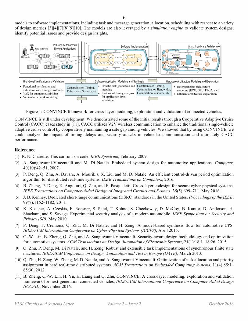
4. Design Operation Fig.3 shows the proposed SA. In addition to the conventional VLSA, the proposed design consists of latching, shorting,
offset storing and data sampling transistors. These additional transistors are used in different phases, because the complete sensing is carried out in different stages. The conventional VLSA comprises of the transistors M8, M9, M10 and M11 while M12 and M13 are used to provide the necessary latching action. To connect the drain and gate of the two NMOS of voltage latch M14 and M15 are used. Transistors M16, M17, M18 and M19 are used to connect the capacitors to the nodes A and B and also to connect to the data sampling transistors.
Figure 3. Proposed Sense Amplifier
Transistors M20, M21, M22, and M23 are used the data from the bit lines and fetch it to the nodes A and B after subtracting the threshold voltages from the capacitors. Initially the nodes C and D are pre-charged to the supply voltage. During pre-charging transistors M25 and M26 are made to conducts by applying pre-charge (PC) signal, while the other transistors are off. Once the pre-charging is done the
M9
LE
M25
LE
M10
BL
M18
PC
D
M8
M26
CB
BLB
M7
M20 M21
PS
PC
C
M23
CA
M11DS
SE
OC OC
D
M24
DS
OC OC
DS
M13
GD
M15
M12
G
M19
M22
M17 M16

10
VLSI Circuits and Systems Letter Volume 2 – Issue 2 October 2016
transistors M14 and M15 are turned on by triggering gate-drain (GD) signal to connect the drain and gate of the transistors M10 and M11, so that they form diodes. At the same time transistors M16, M17, M18 and M19 are also activated by triggering offset-compensation (OC) and hence the threshold voltages of M10 and M11 are stored in the gate capacitors of each transistor. Thereafter, bit line voltages are sampled, at this period the transistors M20, M21, M22 and M23 are turned on by activating data-sample (DS) signal while the other transistors are off. Before reaching to the nodes stored threshold voltages on the capacitors are subtracted from the bit lines voltages.
At last the SA is regenerated; the latching action of SA is activated by turning on transistors M12 and M13 by sense enable (SE) signal. And the sense enable (SE) signal of the transistor M24 is made high to achieve the amplification. This way at this phase the exact output is achieved.
5. Results And Discussion The proposed SA is design and analyzed in 45nm standard CMOS technology and it is capable of compensating 90mV
offset. Read performance is evaluated in terms of sensing delay, which is the time between the 50% rise of SEN signal to the time when, the node which is fully discharging reaches 50% of VDD [10]. And hence this delay is the key factor to define the speed of the SA. For a high speed SA this delay must be low. In the proposed design the delay is reduced considerably. As compare to conventional SA, more number of transistors are used. But due to employed timing strategy the effect on power consumption is low. The exact value of both delay and power is discussed below. In the proposed design the delay is improved by 62.73% as compared to conventional VLSA and by 84.31% as compared to conventional CLSA for different value of supply voltage, the comparison is shown in Fig.4. To gauge the effect of BL capacitance on sensing delay we conducted measurement with varying BL capacitance and shown in Fig. 5. It can be depicted from figure that, delay is improved by 51.28% as compared to VLSA and by 79.8% as compared to CLSA for different value of the bit line capacitance as shown in the same.
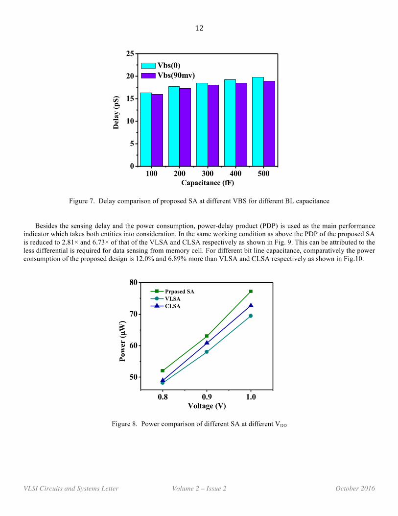
The delay is also analyzed for different values of bulk-to-source (VBS) voltage of M10 and M11. The reason for the same is that the threshold voltage of the transistor also depends upon the VBS, so to incorporate different offset to the circuit the same approach is used. Therefore the SA is simulated for two different values of VBS (0V and 90mV) and the observation makes it clear as in Fig.6 and in Fig.7 that for different voltage supply the delay increases for greater VBS and for the different bit line capacitance the delay decreases respectively. This is due to the reason that, large bit line capacitance takes more time to discharge but with more voltage supply the discharging becomes fast. And hence the delay decreases for greater VBS.
0.80 0.85 0.90 0.95 1.000
50
100
150
200
250
Del
ay (p
S)
Voltage (V)
Proposed SA VLSA CLSA
Figure 4. Delay comparison of different SA at different VDD

11
VLSI Circuits and Systems Letter Volume 2 – Issue 2 October 2016
100 200 300 400 5000
25
50
75
100
125
Del
ay(p
S)
Capacitance (fF)
Proposed SA VLSA CLSA
Figure 5. Delay comparison of different SA at different BL capacitance
The power consumption of the proposed amplifier is approximately 8.06% more than the conventional VLSA while it is 5.99% more than CLSA even after having more number of transistors comparatively as shown in Fig.8.The increase in power consumption is considerably low due to the strategic timing for every phase of the entire design operation. Because during one phase corresponding transistors are on and the remaining transistors are off. For example, during data sampling phase only data sampling transistors are conductive and others are not, also data sensing is enabled only when it is required. This way all time latching action is avoided that consumes power. Hence latching action is avoided that consumes power. Hence increase in power consumption is not much. Power consumption increases with increase in supply voltage
100 200 300 400 5000
5
10
15
20
25
Del
ay (p
S)
Capacitance (fF)
Vbs(0) Vbs(90mv)
Figure 6. Delay comparison of proposed SA at different VBS for different VDD
12
VLSI Circuits and Systems Letter Volume 2 – Issue 2 October 2016
100 200 300 400 5000
5
10
15
20
25
Del
ay (p
S)
Capacitance (fF)
Vbs(0) Vbs(90mv)
Figure 7. Delay comparison of proposed SA at different VBS for different BL capacitance
Besides the sensing delay and the power consumption, power-delay product (PDP) is used as the main performance
indicator which takes both entities into consideration. In the same working condition as above the PDP of the proposed SA is reduced to 2.81× and 6.73× of that of the VLSA and CLSA respectively as shown in Fig. 9. This can be attributed to the less differential is required for data sensing from memory cell. For different bit line capacitance, comparatively the power consumption of the proposed design is 12.0% and 6.89% more than VLSA and CLSA respectively as shown in Fig.10.
0.8 0.9 1.0
50
60
70
80
Pow
er (µ
W)
Voltage (V)
Prposed SA VLSA CLSA
Figure 8. Power comparison of different SA at different VDD

13
VLSI Circuits and Systems Letter Volume 2 – Issue 2 October 2016
Figure 9. Power delay product at various supply voltage
100 200 300 400 50060
65
70
75
80
85
90
Pow
er (µ
W)
Capacitance (fF)
Proposed SA VLSA CLSA
Figure 10. Power comparison of different SA at different BL capacitance
0.8 0.9 1.00
20
40
60
80
Pow
er (µ
W)
Voltage (V)
Vbs(0) Vbs(90mv)
Figure 11. Power comparison of proposed SA at different VBS for different VDD
0.8
0.91.0 0
246810
Proposed
VLSA
CLSA
Proposed VLSA CLSA
Pow
er D
elay
Pro
duct
(fJ)
Supply Voltage (V)

14
VLSI Circuits and Systems Letter Volume 2 – Issue 2 October 2016
100 200 300 400 5000
22
44
66
88
110
Pow
er (µ
W)
Capacitance (fF)
Vbs(0) Vbs(90mv)
Figure 12. Power comparison of proposed SA at different VBS for different BL Capacitance
Also in power analysis the SA is simulated for two different values of VBS (0 and 90mV) and it is shown that in Fig.11
and Fig.12 for different supply voltage the power increases for greater VBS and for the different bit line capacitance the power decreases respectively.
6. Conclusions A new offset compensated sense amplifier has been presented. The descriptive analysis of various parameters like power
and delay is presented and the simulation is carried out for different values of voltage supply and for different bit line capacitance. The result is compared with conventional VLSA and CLSA, and the proposed SA is found better in performance comparatively. Also the proposed amplifier is compared with itself for the different offset values by varying VBS to incorporate different offset in SA. The Offset compensation of 90mv is achieved. References [1] T. Na, S.Woo, J. Kim, H. Jeong and S. O. Jung, (2014) “Comparative study of various latch-type sense amplifiers”,
IEEE Trans. Very Large Scale Integr. (VLSI) Syst., vol. 22, no. 2, pp. 425-429. [2] H. Mostafa, M. Anis, and M. Elmasry, (2013) “Statistical SRAM Read Access Yield Improvement Using Negative
Capacitance Circuits”, IEEE Trans. Very Large Scale Integr. (VLSI) Syst., vol. 21, no. 1, pp. 92–101. [3] R. Singh, and N. Bhat, (2004) “An Offset Compensation Technique for Latch Type Sense Amplifiers in High Speed
Low Power SRAMs”, IEEE Trans. Very Large Scale Integration (VLSI) Systems, Vol. 12, No. 6. [4] J. S. Shah, D. Nairn, M. Sachdev, (2013) “An Energy-Efficient Offset-Cancelling Sense Amplifier,” IEEE
Transactions on Circuits and Systems II: Express Briefs vol. 60, no. 8, pp. 477-481. [5] B. S. Reniwal, V. Vijayvargiya, P. Singh, S. K. Vishvakarma and D. Dwivedi, (2015) “Dataline isolated differential
current feed/mode sense amplifier for small ICell SRAM using FinFET,” in Proc. ACM 25th Great lakes symposiums on VLSI (GLSVLSI),pp. 95-98.
[6] M. Bhargava, M. McCartney, A. Hoefler, and K. Mai, (2009) “Low-overhead, digital offset compensated, SRAM sense amplifiers,” in Proc. IEEE Custom Integr. Circuits Conf., pp. 705–708.
[7] S. J. Lovett, (2001) “Threshold Voltage Mismatch Compensated Sense Amplifier for SRAM Memory Arrays,” U.S. Patent 6 181 62.
[8] P. Beshay, B. H. Calhoun J. f. Ryan, (2012) “Sub-threshold sense amplifier compensation using auto-zeroing circuitry”, IEEE Subthreshold microelectronics conference (subvt), pp.1–3.
[9] P. Beshay, J. Bolus, T. Blalock, V. Chandra, and B. H. Calhoun, (2012) “SRAM Sense Amplifier Offset Cancellation Using BTl Stress” , IEEE, Subthreshold Microelectronics Conference (SubVT),pp.1–3.
[10] X. Conte, (2005) “A high-performance very low-voltage current sense amplifier for non volatile memories”, IEEE J. Solid-State Circuits, vol. 40, no. 2, pp. 507–514.

15
VLSI Circuits and Systems Letter Volume 2 – Issue 2 October 2016
Opinion
Mathematical Models for Latency Estimation of Loop Unrolled and Loop Pipelined CDFGS during High Level Synthesis Anirban Sengupta Discipline of Computer Science and Engineering, Indian Institute of Technology Indore (email: [email protected])
Abstract – This letter presents mathematical models for latency estimation of scheduled loop based control data flow graphs (CDFGs) during High Level Synthesis (HLS). The models are particularly useful when dealing with loop manipulation techniques during high level transformation such as loop unrolling and loop pipelining. Effective utilization can be made when unrolling control data flow graphs for a large value. In such a scenario, standard practice is to exhaustively unroll the loop (for the specified unroll factor value), followed by scheduling of operations based on the available resource constraint. This usually leads to huge code density and runtime when the unroll factor value is large, as latency estimation is only possible when all the operations are unrolled and scheduled. This motivates the need for mathematical models that can accurately estimate the latency of a CDFG without the necessity of tediously unrolling all operations or scheduling all operations (in case of pipelining).
1. Introduction High level synthesis is a process of converting an algorithmic behavior into its register transfer level description which involves a process called design space exploration (DSE) [1,2,3,4,5,6]. DSE typically includes evaluation of a design point with respect to objectives such as latency and chip area. However calculation of latency for loop based CDFGs is non-trivial as it incurs huge code density and runtime. Further, loop manipulation comprises unrolling and pipelining both of which are considered complex tasks. The need of the hour is to use mathematical models that can estimate the latency of a CDFG without requiring to tediously unroll all loops or scheduling all operations.
2. Model for estimating latency of loop unrolled CDFGs Three cases are discussed for loop unrolling. The estimation model is adopted from [7, 8]. Case 1- When unrolling factor (UF) = 1 (Indicates no unrolling)
CT = Cbody * α (1) Where, CT = # Control Steps (CS), Cbody = # CS required to execute loop body once, α = # duplicate loop body iterations Note: No. of CS required to execute loop body one time = no of CS required to execute first loop iteration
( ) quotient quotientloop count Ino of duplicateiterationof loopbody
unrolling factor UFα
⎛ ⎞ ⎛ ⎞= =⎜ ⎟ ⎜ ⎟⎝ ⎠⎝ ⎠
(2)
Using eqns. (1) & (2) above:
(C * ) (C * )
1
,C (C *I)
quotient
T body body
body first
T first
I
UFC
C C andUFSo
α ⎡ ⎤= = ⎢ ⎥⎣ ⎦= =
=
Cfirst= no of CS required for executing the first loop iteration Case 2- When UF > 1 and evenly divides the loop count.
CT=Cfirst*αCfirst=4CSα=I=32CT=4*32=128CS
Fig1.Demonstrativeexampleandcalculationforloopunrollinglatencymodel(adoptedfromSenguptaet.al[8])

16
VLSI Circuits and Systems Letter Volume 2 – Issue 2 October 2016
When the unroll factor value specified evenly divides the maximum iteration count, then the remainder loops are zero. This is specified as: I mod UF = 0 Now, let us formulate the number of control steps required to execute loop body once as: # CS in executing loop body once = Cfirst + (UF-1)* # CS required between initiation of consecutive loop iterations. This is mathematically written as in eqn. (7):
(C ( 1)* )body first IIC UF C= + − (3) Now from eqn. 1:
*T bodyC C α= (4) Combining eqns. (4) and (3), we get eqn. (5):
(C ( 1)* )*T first IIC UF C α= + − (5) Now combining eqns. (5) and (2), we get eqn. (6):
(C ( 1)* ) *T first II
quotientIU
CF
C UF ⎛ ⎞⎜ ⎟
⎠−
⎝= + (6)
Fig.2 shows a demonstrative example for a loop unrolled CDFG. Case 3- when UF > 1 and divides loop count unevenly When the unroll factor value specified unevenly divides the maximum iteration count, then the remainder loops are non- zero. This is specified as: I mod UF ≠ 0 Total number of CS = Number of pipelined CS + Number of sequential CS (7) Number of pipelined CS can be re-written from eqn. 6 as in eqn. (8): (8)
(C ( 1)* )*first IIpipelineCS UF C α= + − Number of sequential CS required is written in eqn. (9): Sequential CS = ( mod )* firstI UF C (9) Substituting eqns. (8) and (9) in eqn. (7) to form eqn. (10):
(C ( 1)* )* ( mod )*T first II firstC UF C I UF Cα= + − + (10) Note: With proposed model (eq. 10), total # of CS can be estimated without performing loop unrolling more than once.
CalculationofCSfromproposedformula:Cfirst=4;CII=2;UF=2;I=32;Substitutevaluesineqn.6:CT=[4+(2-1)*2]*[32/2]quotient=96CSCalculationwithformalmethodCSinoneiteration=6CSNoofiteration=16Totalnoofcontrolstep=16*6=96CS
Loopbody
Fig2.Demonstrativeexampleandcalculationforloopunrollinglatencymodel(withoutremainderloops)(adoptedfromSenguptaet.al[8])

17
VLSI Circuits and Systems Letter Volume 2 – Issue 2 October 2016
Total execution time is calculated using eqn. (11): **((C ( 1)* )* )( mod )*
exe T
first II first
T CUF C I UF Cα
= Δ
= Δ + − + (11)
Where ∆ is delay of one CS in nanosecond Fig.3 shows a demonstrative example for a loop unrolled CDFG
3. Model for estimating latency of loop pipelined CDFGs
This model is described in details in [9]. Another well-known high level transformation technique is called ‘loop pipelining’ that improves performance. The process of loop pipelining is achieved by ‘resource constraint software pipelining’. It is a process by which the next iteration in the loop initiates before the previous iteration finishes. The completely loop body needs to be unrolled as per the value specified for loop unrolling. The resource constraint scheduling is continued until a pattern emerges. Once the pattern is detected, then scheduling is stopped. An example of resource constrained loop pipelining for FIR is shown in Fig. 4. A pattern is detected between a set of every two consecutive iterations i.e. i & i+1 (group X1) and i+2 & i+3 (group X2). The delay of the first group is denoted by DG and the cycle time (difference between
two consecutive groups X1 & X2) is denoted by CTG, I = total number of iterations of the loop, N = number of hardware
Fig4.ResourceConstrainedLoopPipeliningbasedon2(*),2(+),1(<)withmaximumeightiterations(forFIRbenchmark)(SourceextractedfromSenguptaet.al[9)
i+2 i+3*
+
*
* *
* *
* *
+
++
++
++
i i+1
i+4 i+5
i+6 i+7
DG=578CS
CG=550CS
550CS
578CS
1128CS
564CS
1100CS
X1
X2
DG=578CS,CG=550CS
I=8,N=2,Δ=20ns
𝑇#$ = {𝐷( + *𝐼𝑁− 1/ . 𝐶2( }∆
=44,560ns
Fig3.Demonstrativeexampleandcalculationforloopunrollinglatencymodel(withremainderloops)(adoptedfrom
Senguptaet.al[7,8])

18
VLSI Circuits and Systems Letter Volume 2 – Issue 2 October 2016
instances corresponding to the maximum parallel independent operations and ∆ = duration of one CS during operation chaining based scheduling. This pattern enables to estimate the total execution time (TSP) of the CDFG without requiring to tediously schedule remaining iterations viz. i+4, i+5, i+6. Therefore, latency model for loop pipelining is given in eqn. (12) adopted from [9] is:
𝑇#$ = {𝐷( +56− 1 . 𝐶2(}∆
(12)
4. Conclusion This letter presented two mathematical models that could be used for latency calculation of loop unrolled CDFG and
loop pipelined CDFG during high level synthesis. Often loop unrolling becomes tedious and time consuming which affects latency calculation process in high level synthesis. The models provide a good estimate of the final latency of the scheduled CDFG without requiring to exhaustively unroll all the loops. The other model for loop pipelining also estimates the latency without requiring scheduling all the operation.
Reference [1] M. Holzer, B. Knerr and M. Rupp, “Design space exploration with evolutionary multi-objective optimization,”
International Symposium on Industrial Embedded Systems, 2007, pp.126-133. [2] A. Sengupta, R. Sedaghat and Z. Zeng, “A high level synthesis design flow with a novel approach for efficient design
space exploration in case of multi-parametric optimization objective,” Microelectronics Reliability Elsevier, vol. 50, no. 3, pp. 424-437, 2010.
[3] V. Krishnan and S. Katkoori, “A genetic algorithm for the design space exploration of datapaths during high-level synthesis,” IEEE Trans. on Evolutionary Computation, vol.10, no.3, pp. 213-229, 2006.
[4] V. Heijlingers, L. Cluitmans and J. Jess, “High-level synthesis scheduling and allocation using genetic algorithms”, Asia South Pacific Design Automation Conference, pp.61-66, 1995.
[5] A. Sengupta, R. Sedaghat and P. Sarkar, “A multi structure genetic algorithm for integrated design space exploration of scheduling and allocation in high level synthesis for DSP kernels,” Swarm and Evolutionary Computation, pp. 35-46, Vol. 7, 2012
[6] R. Harish., M. Bhuvaneswari and S. Prabhu, “A novel framework for applying multiobjective GA and PSO based approaches for simultaneous area, delay, and power optimization in high level synthesis of datapaths,” VLSI Design, Article ID 273276, 2012.
[7] A Sengupta, VK Mishra, "Swarm Intelligence Driven Simultaneous Adaptive Exploration of Datapath and Loop Unrolling Factor during Area-Performance Tradeoff ",Proceedings of 13th IEEE Computer Society Annual International Symposium on VLSI (ISVLSI), Florida, July 2014, pp. 106 112.
[8] A Sengupta, VK Mishra "Automated Exploration of Datapath and Unrolling Factor during Power-Performance Tradeoff in Architectural Synthesis Using Multi-Dimensional PSO Algorithm", Elsevier Journal on Expert Systems With Applications, Volume 41, Issue 10, August 2014,pp. 46914703.
[9] A Sengupta, SP. Mohanty "High-Level Synthesis of Digital Circuits in the Nanoscale, Mobile Electronics Era", IET Book: Nano-CMOS and Post-CMOS Electronics: Circuits and Design, (Eds: Saraju P Mohanty& Ashok Srivastava), Invited Book Chapter, e-ISBN: 9781785610004, pp: 219 - 261, June 2016.
Bio: Dr. Anirban Sengupta is currently an Assistant Professor in Discipline of Computer Science and Engineering at Indian Institute of Technology (IIT) Indore, where he directs the research lab on ‘Behavioural Synthesis of Digital IP core’. He holds a Ph.D. & M.A.Sc. in Electrical & Computer Engineering from Ryerson University, Toronto (Canada) and is a registered Professional Engineer of Ontario (P.Eng.). In the past, he was also affiliated with Indian Institute of Science (IISc) Bangalore as a visiting research scholar. He holds an ‘Honorary Chief Scientist’ position at VividSparks IT Solutions Pvt. Ltd. as external affiliation besides his regular affiliation at IIT Indore. His research projects are funded by DST- SERB and Media Lab Asia. He has more than 100 Publications & Patents. He serves in Editorial positions of 8 IEEE, Elsevier, & IET Journals. He is currently serving as Editor of Elsevier Microelectronics Journal, Associate Editor of IET Journal on Computer & Digital Techniques, Executive Editor of IEEE Consumer Electronics (M-CE), Associate Editor of IEEE VLSI Circuits & Systems Letter and IEEE Access Journal. He further serves as Guest Editor of IEEE Transactions on Consumer Electronics and IEEE Transactions on VLSI Systems.

19
VLSI Circuits and Systems Letter Volume 2 – Issue 2 October 2016
Updates
Upcoming Conferences/Workshops • ARITH: IEEE Symposium on Computer Arithmetic, London (UK), July 24-26, 2017; deadline: December 31,
2016; web: http://arith24.arithsymposium.org/ • ISVLSI: IEEE Computer Society Annual Symposium on VLSI, July 3-5, 2017, Bochum (Germany); deadline:
February 24, 2017; web: http://www.isvlsi.org/ • ASYNC: IEEE International Symposium on Asynchronous Circuits and Systems, San Diego, CA (USA), May
2017; web: http://asyncsymposium.org/async/Welcome.html • ECMSM: IEEE International Workshop of Electronics, Control, Measurement, Signals and their application to
Mechatronics, Donosti-San Sebastian, May 24-27, 2017; deadline: January 27, 2017; web: http://ecmsm2017.mondragon.edu/en
• DATE: The Design, Automation and Test in Europe, Lausanne (Switzerland), March 27-31, 2017; web: https://www.date-conference.com/
• ISQED: The 18th International Symposium on Quality Electronic Design, Santa Clara, CA (USA), March 13-15, 2017; web: http://www.isqed.org/
• ASP-DAC: The 22nd Asia and South Pacific Design Automation Conference, Chiba/Tokyo, Japan, January 16-19, 2017; web: http://www.aspdac.com/aspdac2017/
• VLSID: 30th International Conference on VLSI Design, Hyderabad (India), January 7-11, 2017; web: http://vlsiconference.com/
• iNIS: IEEE International Symposium on Nanoelectronic and Information Systems, Gwalior (India), December 19-21, 2016; web: http://www.ieee-inis.org/
• ICCAD: IEEE International Conference on Computer Aided Design, Texas, November 7-10, 2016; web: https://iccad.com/
• MICRO: IEEE/ACM International Symposium on Microarchitecture, Taiwan, October 15-19, 2016; web: http://www.microarch.org/micro49/
• ICM: IEEE International Conference on Microelectronics, Egypt, December 17-20, 2016; web: http://www.ieeeicm2016.org/
• ESWEEK: Embedded Systems Week, Pittsburgh, PA (USA), October 2-7, 2017; web: http://www.esweek.org/
Awards 1. The best paper award of ACSD 2016 was awarded to this paper:
Raymond Devillers: Products of Transition Systems and Additions of Petri Nets 2. The best paper award for ASYNC 2016 went to:
Ring Oscillator Clocks and Margins Jordi Cortadella, Marc Lupon, Alberto Moreno, Antoni Roca and Sachin Sapatnekar
3. TCVLSI Student Travel Awards at SLIP 2106:
a. Mohammad Ahmed [email protected] Portland State University b. Scott Lerner [email protected] Drexel University
4. The Best Paper Award winner of SLIP'16 is as follows: A Comparative Analysis of Front-End and Back-End Compatible Silicon Photonic On-Chip Interconnects Ishan G Thakkar, Sai Vineel Reddy Chittamuru, Sudeep Pasricha Department of Electrical and Computer Engineering Colorado State University, Fort Collins, CO, U.S.A.

20
VLSI Circuits and Systems Letter Volume 2 – Issue 2 October 2016
5. Following ISVLSI 2016 awards:
2 student travel awards: Maria Malik, George Mason University, USA Sunil Kumar Maddikatla, IIIT Hyderabad, India
TCVLSI best paper award: Sunil Kumar Maddikatla and Srivatsava Jandhyala: An Accurate CMOS Integrated Temperature Sensor For IOT Applications
Amar Mukherjee Best Paper Award: Innocent Agbo, Mottaqiallah Taouil, Said Hamdioui, Pieter Weckx, Stefan Cosemans, Praveen Raghavan, Francky Catthoor and Wim Dehaene: Quantification of Sense Amplifier Offset Voltage Degradation due to Zero- and Run-time Variability
Best Poster Award: Jaya Dofe, Yuejun Zhang and Qiaoyan Yu: DSD: A Dynamic State-Deflection Method for Gate-Level Netlist Obfuscation

21
VLSI Circuits and Systems Letter Volume 2 – Issue 2 October 2016
Outreach and Community
Developing and Sustaining Computing Based Outreach Experiences Mike Borowczak Erebus Labs and Consulting, Laramie, Wyoming USA Andrea C Burrows Department of Secondary Education, University of Wyoming, Laramie, WY, USA Two of the challenges in creating viable outreach opportunities in the field of computing include long term sustainability and tool accessibility by participants after they leave an experiential session. When trying to extend a research experience to satisfy some set of broader impacts the challenge remains how to share tools and infrastructure located within a research or university domain with non-university members (e.g. K-12 students and teachers). Some grants, such as National Science Foundation Research Experiences for Teachers (RET) and Research Experiences for Undergraduates (REU), allow for the purchase of personal computing devices which could be set up with a proper toolchain given your specific requirements. This approach, while flexible, is not only costly, but also comes at a significant cost in upkeep, administration, and tracking. This article highlights the use of cloud based solution in delivering a consistent, easily managed, available anywhere, access point to a code development and sharing platform. Mixed-mode notebooks, containing code, output and markup are an emerging solution for code sharing within academic and business communities. One popular notebook platform, Jupyter, emerged from IPython a platform capable of hosting python notebooks. Figure 1 shows the basic layout for Ipython notebooks, which includes a menu bar with common editing menus, and multiple cell types including: a Markup Cell with LaTeX, an Input Cell, and an Output Cell with rendered graphics. Jupyter, a rebranding and refactoring of IPython allows different compute kernels to be served to a user through a browser interface. A list of currently available kernels (75 as of September 2016) is located here. The first author is working on developing three additional kernels for Magic, Spice and VHDL for use in VLSI courses and outreach. While Jupyter can be installed on any machine (installation instructions are available on Jupyter.org), Jupyter notebooks become more powerful when hosted in conjunction with JupyterHub - a tool which allows for the rendering of Jupyter notebooks to a set of users. Imagine creating and maintaining a single environment and then sharing access to copy of that environment to a set of users - regardless of physical location, computing platform, or system administrator skill set. That’s exactly what UWRAMPED, a 2016 summer professional development, accomplished. The University of Wyoming Robotics, Applied Mathematics, Physics and Engineering Design teacher professional development (uwramped.org) hosted six mini-professional developments - one of which focused on Python programming for applied physics and astronomy research. From start to finish, the deployment of a JupyterHub platform, capable of serving 20 teachers at once, took less than an hour to set up at a cost of $40-$80 a month - all on a remote cloud based host. For those interested, details for the installation and setup follows. A minimal install can cost as little as $5/month.
22
VLSI Circuits and Systems Letter Volume 2 – Issue 2 October 2016
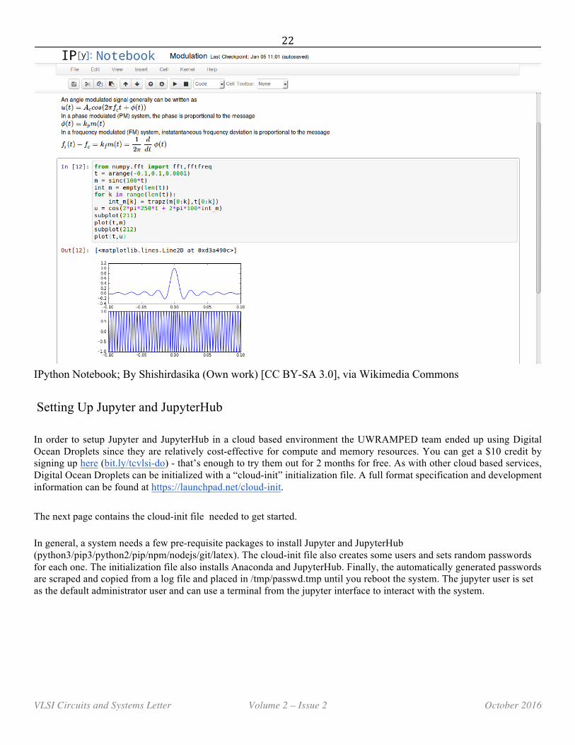
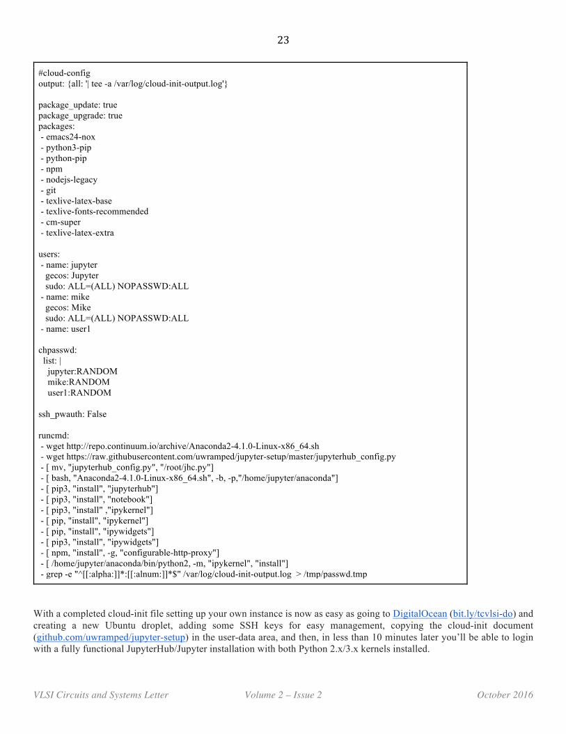
IPython Notebook; By Shishirdasika (Own work) [CC BY-SA 3.0], via Wikimedia Commons Setting Up Jupyter and JupyterHub In order to setup Jupyter and JupyterHub in a cloud based environment the UWRAMPED team ended up using Digital Ocean Droplets since they are relatively cost-effective for compute and memory resources. You can get a $10 credit by signing up here (bit.ly/tcvlsi-do) - that’s enough to try them out for 2 months for free. As with other cloud based services, Digital Ocean Droplets can be initialized with a “cloud-init” initialization file. A full format specification and development information can be found at https://launchpad.net/cloud-init. The next page contains the cloud-init file needed to get started. In general, a system needs a few pre-requisite packages to install Jupyter and JupyterHub (python3/pip3/python2/pip/npm/nodejs/git/latex). The cloud-init file also creates some users and sets random passwords for each one. The initialization file also installs Anaconda and JupyterHub. Finally, the automatically generated passwords are scraped and copied from a log file and placed in /tmp/passwd.tmp until you reboot the system. The jupyter user is set as the default administrator user and can use a terminal from the jupyter interface to interact with the system.
23
VLSI Circuits and Systems Letter Volume 2 – Issue 2 October 2016
#cloud-config output: {all: '| tee -a /var/log/cloud-init-output.log'} package_update: true package_upgrade: true packages: - emacs24-nox - python3-pip - python-pip - npm - nodejs-legacy - git - texlive-latex-base - texlive-fonts-recommended - cm-super - texlive-latex-extra users: - name: jupyter gecos: Jupyter sudo: ALL=(ALL) NOPASSWD:ALL - name: mike gecos: Mike sudo: ALL=(ALL) NOPASSWD:ALL - name: user1 chpasswd: list: | jupyter:RANDOM mike:RANDOM user1:RANDOM ssh_pwauth: False runcmd: - wget http://repo.continuum.io/archive/Anaconda2-4.1.0-Linux-x86_64.sh - wget https://raw.githubusercontent.com/uwramped/jupyter-setup/master/jupyterhub_config.py - [ mv, "jupyterhub_config.py", "/root/jhc.py"] - [ bash, "Anaconda2-4.1.0-Linux-x86_64.sh", -b, -p,"/home/jupyter/anaconda"] - [ pip3, "install", "jupyterhub"] - [ pip3, "install", "notebook"] - [ pip3, "install" ,"ipykernel"] - [ pip, "install", "ipykernel"] - [ pip, "install", "ipywidgets"] - [ pip3, "install", "ipywidgets"] - [ npm, "install", -g, "configurable-http-proxy"] - [ /home/jupyter/anaconda/bin/python2, -m, "ipykernel", "install"] - grep -e "^[[:alpha:]]*:[[:alnum:]]*$" /var/log/cloud-init-output.log > /tmp/passwd.tmp
With a completed cloud-init file setting up your own instance is now as easy as going to DigitalOcean (bit.ly/tcvlsi-do) and creating a new Ubuntu droplet, adding some SSH keys for easy management, copying the cloud-init document (github.com/uwramped/jupyter-setup) in the user-data area, and then, in less than 10 minutes later you’ll be able to login with a fully functional JupyterHub/Jupyter installation with both Python 2.x/3.x kernels installed.

24
VLSI Circuits and Systems Letter Volume 2 – Issue 2 October 2016
Now login to your newly created image, move your passwords, and run the following commands: screen -q -S jupyter su - jupyter -c '/usr/local/bin/jupyterhub -f jhc.py --no-ssl' Ctrl+a Ctrl+d (to detach screen)
You should really set up SSL but that’s beyond the scope of this brief introduction.
Now, go to http://yourhost-ip:8000 and login with jupyter credentials (from password file - /tmp/myPasswords.tmp), from there you can then follow any Jupyter tutorial you wish!

25
VLSI Circuits and Systems Letter Volume 2 – Issue 2 October 2016
Faculty Spotlight
Do you have outreach or educational experiences that you would like to share? If you would like to be featured in the next issue of TCVLSI’s newsletter, or if you would like to nominate someone to featured in the next issue send an email to [email protected] with details and contact information.
Take the VLSI Education Survey
Is VLSI education keeping pace or advancing engineering education best practices? If so, where are the results of our current practices and advances? Without a detailed survey of current practices, answers to these questions remain elusive. TCVLSI members are encouraged to take and distribute the following survey to their peers and students. Results will be shared in an upcoming issue of VCAL. The survey is available online here: http://bit.ly/tcvlsi-ed-survey.
A Puzzle for All Have a puzzle? Do you want to try to stump your colleagues? Send your puzzle ideas to [email protected] and you might see it featured here!

26
VLSI Circuits and Systems Letter Volume 2 – Issue 2 October 2016
Call for Contributions
The VLSI Circuits and Systems Letter aims to provide timely updates on technologies, educations and opportunities related to VLSI circuits and systems for TCVLSI members. The letter will be published twice a year and it contains the following sections: • Features: selective short papers within the technical scope of TCVLSI, “What is” section to introduce interesting topics
related to TCVLSI, and short review/survey papers on emerging topics in the areas of VLSI circuits and systems. • Opinions: Discussions and book reviews on recent VLSI/nanoelectronic/emerging circuits and systems for nano
computing, and “Expert Talks” to include the interviews of eminent experts for their concerns and predictions on cutting-edge technologies.
• Updates: Upcoming conferences/workshops of interest to TCVLSI members, call for papers of conferences and journals for TCVLSI members, funding opportunities and job openings in academia or industry relevant to TCVLSI members, and TCVLSI member news.
• Outreach and Community: The “Outreach K20” section highlights integrating VLSI computing concepts with activities for K-4, 4-8, 9-12 and/or undergraduate students. It also features student fellowship information as well a “Puzzle” section for our readership.
We are soliciting contributions to all these four sections. Please directly contact the editors and/or associate editors by email to submit your contributions.
Submission Deadline: All contributions must be submitted by March 7, 2017 in order to be included in the April issue of the letter.
Editors: • Saraju Mohanty, University of North Texas, USA, [email protected] • Xin Li, Carnegie Mellon University, USA, [email protected] Associate Editors: • Executive: Yiyu Shi, University of Notre Dame, USA, [email protected] • Features: Shiyan Hu, Michigan Technological University, USA, [email protected] • Features: Qi Zhu, University of California, Riverside, [email protected] • Opinions: Jawar Singh, Indian Institute of Information Technology, Design and Manufacturing, Jabalpur, India,
[email protected] • Opinions: Prasun Ghosal, Indian Institute of Engineering Science and Technology, India, [email protected] • Updates: Helen Li, University of Pittsburg, USA, [email protected] • Updates: Anirban Sengupta, Indian Institute of Technology, Indore, India, [email protected] • Outreach and Community: Mike Borowczak, Erebus Labs & Consulting LLC, USA, [email protected]
Related Documents