Appl. Phys. Lett. 118, 163105 (2021); https://doi.org/10.1063/5.0045090 118, 163105 © 2021 Author(s). Violet phosphorus surface chemical degradation in comparison to black phosphorus Cite as: Appl. Phys. Lett. 118, 163105 (2021); https://doi.org/10.1063/5.0045090 Submitted: 22 January 2021 . Accepted: 05 April 2021 . Published Online: 22 April 2021 Alireza Fali, Michael Snure, and Yohannes Abate COLLECTIONS This paper was selected as an Editor’s Pick

Welcome message from author
This document is posted to help you gain knowledge. Please leave a comment to let me know what you think about it! Share it to your friends and learn new things together.
Transcript
Appl. Phys. Lett. 118, 163105 (2021); https://doi.org/10.1063/5.0045090 118, 163105
© 2021 Author(s).
Violet phosphorus surface chemicaldegradation in comparison to blackphosphorus
Cite as: Appl. Phys. Lett. 118, 163105 (2021); https://doi.org/10.1063/5.0045090Submitted: 22 January 2021 . Accepted: 05 April 2021 . Published Online: 22 April 2021
Alireza Fali, Michael Snure, and Yohannes Abate
COLLECTIONS
This paper was selected as an Editor’s Pick
Violet phosphorus surface chemical degradationin comparison to black phosphorus
Cite as: Appl. Phys. Lett. 118, 163105 (2021); doi: 10.1063/5.0045090Submitted: 22 January 2021 . Accepted: 5 April 2021 .Published Online: 22 April 2021
Alireza Fali,1 Michael Snure,2 and Yohannes Abate1,a)
AFFILIATIONS1Department of Physics and Astronomy, University of Georgia, Athens, Georgia 30602, USA2Air Force Research Laboratory, Sensors Directorate, Wright Patterson Air Force Base, Ohio 45433, USA
a)Author to whom correspondence should be addressed: [email protected]
ABSTRACT
Bulk growth methods have made it possible to synthesize several allotropes of phosphorus such as black, white, red, and violet phosphorus.However, unlike exfoliated black phosphorus (BP), which has been extensively studied, much of the optoelectronic properties and stability ofthe other allotropes have yet to be comprehensively investigated. Here, we study the chemical degradation of exfoliated violet phosphorus(VP) in comparison to BP under ambient conditions using nanoscale infrared spectroscopy and imaging. We identify oxidized phosphorusspecies that result from chemical reaction processes on the surfaces of these phosphorus allotropes. We have found that VP exhibits anoticeably different and slower degradation process when compared to BP, establishing it as the more stable of the two allotropes. A betterunderstanding of the stability of VP could lead to the further fundamental study of its monolayer form for potential future applications.
Published under license by AIP Publishing. https://doi.org/10.1063/5.0045090
Black phosphorus (BP) has been synthesized for over 100 years,1
but the interest in BP in contemporary materials research accelerateddue to its exfoliable nature, which makes it a member of the van derWaals materials (vdW) family. BP’s orthorhombic crystal structurewith a space group Cmca is an anisotropic in-plane displaying twoindependent in-plane components of the dielectric tensor that are dif-ferent from each other.2 The bandgap of BP is tunable, direct, and nar-row, making it suitable for nanoelectronics and nanophotonicsapplications.3 It also displays thickness dependent on/off current ratioin the range of 103–105 and decent saturation characteristics thatmake it a candidate for digital logic applications in thin film electronicsas well as flexible electronics.4 In addition to BP, there are two otherlayered allotropes of phosphorus: violet and blue. These allotropes,which are all p-type, have distinct structures and band gaps rangingfrom narrow BP (0.3 eV)5 to mid bandgap violet phosphorus (VP)(1.7 eV)6 and blue phosphorus (2 eV).7
vdW heterostructures based on BP have presented great opportu-nities for application in nanoelectronics.8 For instance, the Schottkybarrier height and doping of BP can be controlled by electrostatic gat-ing in graphene/BP heterostructures, and BP/MoS2 p–n junctionsshow strong gate-tunable current-rectifying I–V characteristics.9 Withmultiple layered allotropes, phosphorus offers the unique opportunityto form 2D heterostructures using this single element. Recently, thework function and bandgap of VP were investigated, showing an
increasing work function from 4.79 to 5.17 eV with decreasing numberof layers from bulk, while the bandgap increases from 1.7 to �2eV.6Coupled with the thickness tunable bandgap (0.3–1.5 eV)10 and workfunction (4.56–5.17 eV) of BP, this suggests both type I and type II het-erostructures may be possible with BP/VP via thickness tuning.Experimentally, heterostructures of BP/VP have been observed duringchemical vapor transport (CVT) synthesis11 and by annealing BPflakes in tertiarybutylphosphine (TBP).
Oxidation and degradation of BP films remain a considerablechallenge affecting charge impurities in the surface and substrate envi-ronment resulting in scattering centers that can significantly reducethe carrier mobility. Researchers have been endeavoring to acceleratethe use of BP by overcoming the formidable challenge of preservingthin BP from oxidation.4 In addition to ongoing efforts to find ways tostabilize BP, the search for other more stable phosphorus allotropesand phosphorous-based heterostructures is under way. A recent exam-ple is the successful exfoliation of violet phosphorene from bulk VPcrystals grown by CVT.6,12 Although BP has been largely reported asthe most stable phosphorus allotrope, Zhang et al.6 recently reportedVP to be thermally stable to 512 �C compared to 460 �C for BP.However, much of VP’s ambient stability in comparison to BPremains unknown.
In this work, we investigate the surface chemical degradation ofexfoliated VP flakes and compare its surface oxidation with BP
Appl. Phys. Lett. 118, 163105 (2021); doi: 10.1063/5.0045090 118, 163105-1
Published under license by AIP Publishing
Applied Physics Letters ARTICLE scitation.org/journal/apl
samples under ambient conditions over time. We performed nano-scale infrared spectroscopy (nano-FTIR) in the frequency range of800–1500 cm�1 by mapping the local ambient spectral changes atnanometer spatial resolution. The nano-FTIR spectra taken on VPand BP flakes show broad spectra arising from several overlappingvibrational modes from phosphoric species produced due to degrada-tion. The topography and surface degradation evolution of VP flakesare different from surface and height changes observed on BP flakes.VP shows more stability than BP as revealed by the surface topo-graphic and dielectric changes on the surface over time. In BP, the deg-radation begins at random locations as bubbles then evolves abruptlyover a large area via the connection of local bubbles toward saturationfollowing a sigmoid growth curve. The degradation effects we observein VP through topography and nano-FTIR spectra are noticeably dif-ferent from BP, which highlight differences in the degradation processof these two phosphorus allotropes. Additionally, we identify the for-mation of VP on BPs flakes during annealing under TBP, demonstrat-ing the possibility of forming VP/BP heterostructures. The 2Dphosphorous semiconductor allotrope family spans a wide range ofoptoelectronic properties; their combination would allow the uniqueopportunity to build a single-element vdW heterostructure.
Flakes of BP and VP were transferred from bulk sources ontoSiO2/Si for characterization. Bulk BP produced by CVT was purchasedfrom 2D semiconductors, and the bulk VP was produced in-house bychemical vapor deposition (CVD). For VP synthesis, a quartz cruciblewas loaded into the CVD chamber filled with 0.1g SnI4 and 0.1g Snmetal and covered with a sapphire wafer, evacuated, and filled withN2:H2 (95%:5%) to a pressure of 700Torr. Then, the reactor washeated to 600 �C, and the phosphorus source TBP was flowed at a flowrate of 40 sccm with 160 sccm of N2:H2 for 30min. The reactor wasthen cooled to 400 �C under flowing TBP and N2:H2. After reaching400 �C, TBP was turned off and the reactor cooled to room tempera-ture. Small flakes of VP that formed on the edges of the crucible andsapphire wafer were transferred to SiO2/Si for characterization using apolydimethylsiloxane (PDMS) stamp. For VP/BP samples, BP flakeswere exfoliated onto a SiO2/Si substrate, loaded into the CVD cham-ber, evacuated, and filled with N2:H2 to a pressure of 700Torr. Thereactor was then heated to 450 �C under flowing N2:H2. After reachingtemperature, TBP was introduced at a flow rate of 40 sccm for 10minand then cooled to 400 �C before turning off TBP and cooling to roomtemperature.
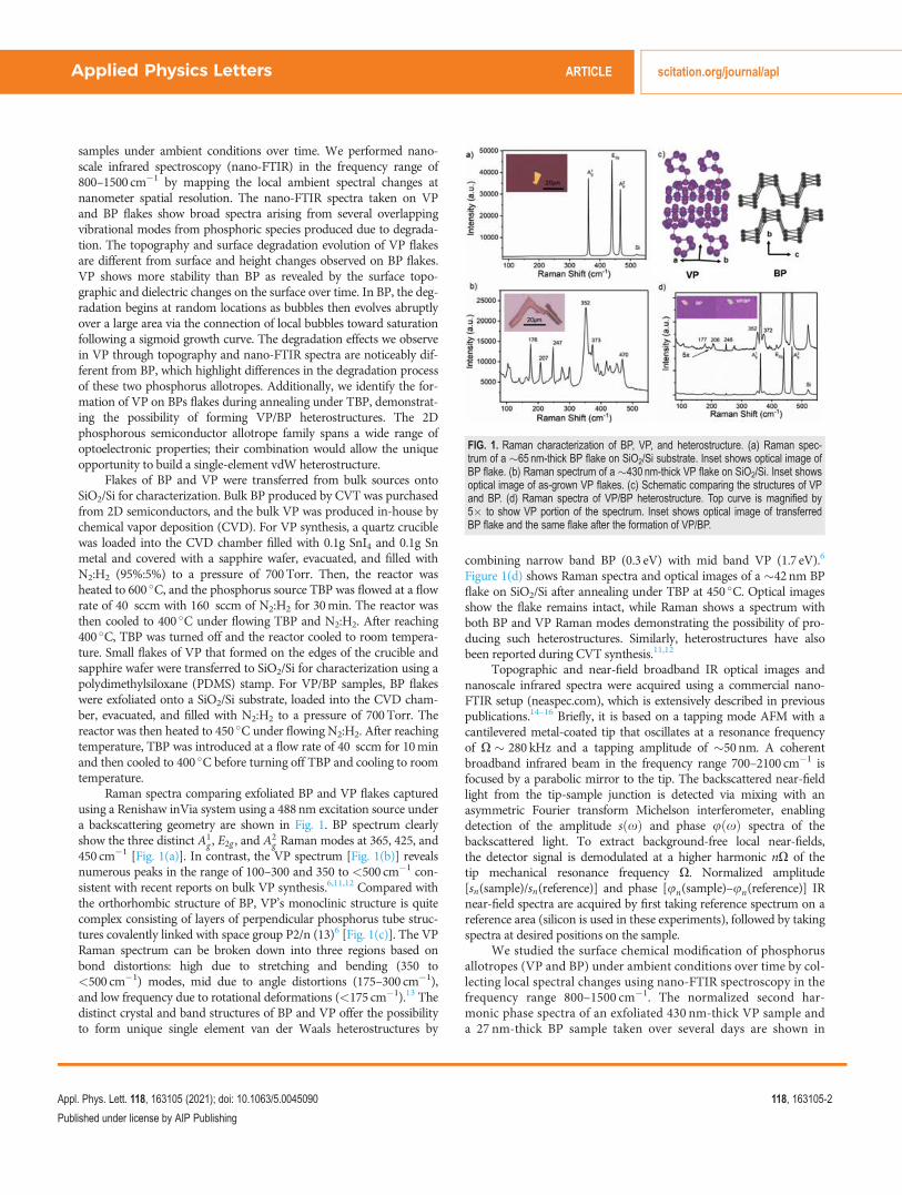
Raman spectra comparing exfoliated BP and VP flakes capturedusing a Renishaw inVia system using a 488nm excitation source undera backscattering geometry are shown in Fig. 1. BP spectrum clearlyshow the three distinct A1
g , E2g , and A2g Raman modes at 365, 425, and
450 cm�1 [Fig. 1(a)]. In contrast, the VP spectrum [Fig. 1(b)] revealsnumerous peaks in the range of 100–300 and 350 to <500 cm�1 con-sistent with recent reports on bulk VP synthesis.6,11,12 Compared withthe orthorhombic structure of BP, VP’s monoclinic structure is quitecomplex consisting of layers of perpendicular phosphorus tube struc-tures covalently linked with space group P2/n (13)6 [Fig. 1(c)]. The VPRaman spectrum can be broken down into three regions based onbond distortions: high due to stretching and bending (350 to<500 cm�1) modes, mid due to angle distortions (175–300 cm�1),and low frequency due to rotational deformations (<175 cm�1).13 Thedistinct crystal and band structures of BP and VP offer the possibilityto form unique single element van der Waals heterostructures by
combining narrow band BP (0.3 eV) with mid band VP (1.7 eV).6
Figure 1(d) shows Raman spectra and optical images of a �42nm BPflake on SiO2/Si after annealing under TBP at 450 �C. Optical imagesshow the flake remains intact, while Raman shows a spectrum withboth BP and VP Raman modes demonstrating the possibility of pro-ducing such heterostructures. Similarly, heterostructures have alsobeen reported during CVT synthesis.11,12
Topographic and near-field broadband IR optical images andnanoscale infrared spectra were acquired using a commercial nano-FTIR setup (neaspec.com), which is extensively described in previouspublications.14–16 Briefly, it is based on a tapping mode AFM with acantilevered metal-coated tip that oscillates at a resonance frequencyof X � 280 kHz and a tapping amplitude of �50nm. A coherentbroadband infrared beam in the frequency range 700–2100 cm�1 isfocused by a parabolic mirror to the tip. The backscattered near-fieldlight from the tip-sample junction is detected via mixing with anasymmetric Fourier transform Michelson interferometer, enablingdetection of the amplitude sðxÞ and phase uðxÞ spectra of thebackscattered light. To extract background-free local near-fields,the detector signal is demodulated at a higher harmonic nX of thetip mechanical resonance frequency X. Normalized amplitude[sn(sample)/sn(reference)] and phase [un(sample)–un(reference)] IRnear-field spectra are acquired by first taking reference spectrum on areference area (silicon is used in these experiments), followed by takingspectra at desired positions on the sample.
We studied the surface chemical modification of phosphorusallotropes (VP and BP) under ambient conditions over time by col-lecting local spectral changes using nano-FTIR spectroscopy in thefrequency range 800–1500 cm�1. The normalized second har-monic phase spectra of an exfoliated 430 nm-thick VP sample anda 27 nm-thick BP sample taken over several days are shown in
FIG. 1. Raman characterization of BP, VP, and heterostructure. (a) Raman spec-trum of a �65 nm-thick BP flake on SiO2/Si substrate. Inset shows optical image ofBP flake. (b) Raman spectrum of a �430 nm-thick VP flake on SiO2/Si. Inset showsoptical image of as-grown VP flakes. (c) Schematic comparing the structures of VPand BP. (d) Raman spectra of VP/BP heterostructure. Top curve is magnified by5� to show VP portion of the spectrum. Inset shows optical image of transferredBP flake and the same flake after the formation of VP/BP.
Applied Physics Letters ARTICLE scitation.org/journal/apl
Appl. Phys. Lett. 118, 163105 (2021); doi: 10.1063/5.0045090 118, 163105-2
Published under license by AIP Publishing
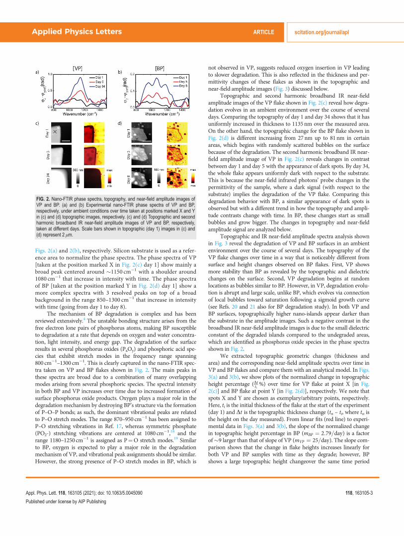
Figs. 2(a) and 2(b), respectively. Silicon substrate is used as a refer-ence area to normalize the phase spectra. The phase spectra of VP[taken at the position marked X in Fig. 2(c) day 1] show mainly abroad peak centered around �1150 cm�1 with a shoulder around1080 cm�1 that increase in intensity with time. The phase spectraof BP [taken at the position marked Y in Fig. 2(d) day 1] show amore complex spectra with 3 resolved peaks on top of a broadbackground in the range 850–1300 cm�1 that increase in intensitywith time (going from day 1 to day 8).
The mechanism of BP degradation is complex and has beenreviewed extensively.4 The unstable bonding structure arises from thefree electron lone pairs of phosphorus atoms, making BP susceptibleto degradation at a rate that depends on oxygen and water concentra-tion, light intensity, and energy gap. The degradation of the surfaceresults in several phosphorus oxides (PxOy) and phosphoric acid spe-cies that exhibit stretch modes in the frequency range spanning800 cm�1–1300 cm�1. This is clearly captured in the nano-FTIR spec-tra taken on VP and BP flakes shown in Fig. 2. The main peaks inthese spectra are broad due to a combination of many overlappingmodes arising from several phosphoric species. The spectral intensityin both BP and VP increases over time due to increased formation ofsurface phosphorus oxide products. Oxygen plays a major role in thedegradation mechanism by destroying BP’s structure via the formationof P–O–P bonds; as such, the dominant vibrational peaks are relatedto P–O stretch modes. The range 870–950 cm�1 has been assigned toP–O stretching vibrations in Ref. 17, whereas symmetric phosphate(PO2-) stretching vibrations are centered at 1080 cm�1,18 and therange 1180–1250 cm�1 is assigned as P¼O stretch modes.19 Similarto BP, oxygen is expected to play a major role in the degradationmechanism of VP, and vibrational peak assignments should be similar.However, the strong presence of P–O stretch modes in BP, which is
not observed in VP, suggests reduced oxygen insertion in VP leadingto slower degradation. This is also reflected in the thickness and per-mittivity changes of these flakes as shown in the topographic andnear-field amplitude images (Fig. 3) discussed below.
Topographic and second harmonic broadband IR near-fieldamplitude images of the VP flake shown in Fig. 2(c) reveal how degra-dation evolves in an ambient environment over the course of severaldays. Comparing the topography of day 1 and day 34 shows that it hasuniformly increased in thickness to 1135nm over the measured area.On the other hand, the topographic change for the BP flake shown inFig. 2(d) is different increasing from 27nm up to 81nm in certainareas, which begins with randomly scattered bubbles on the surfacebecause of the degradation. The second harmonic broadband IR near-field amplitude image of VP in Fig. 2(c) reveals changes in contrastbetween day 1 and day 5 with the appearance of dark spots. By day 34,the whole flake appears uniformly dark with respect to the substrate.This is because the near-field infrared photons’ probe changes in thepermittivity of the sample, where a dark signal (with respect to thesubstrate) implies the degradation of the VP flake. Comparing thisdegradation behavior with BP, a similar appearance of dark spots isobserved but with a different trend in how the topography and ampli-tude contrasts change with time. In BP, these changes start as smallbubbles and grow bigger. The changes in topography and near-fieldamplitude signal are analyzed below.
Topographic and IR near-field amplitude spectra analysis shownin Fig. 3 reveal the degradation of VP and BP surfaces in an ambientenvironment over the course of several days. The topography of theVP flake changes over time in a way that is noticeably different fromsurface and height changes observed on BP flakes. First, VP showsmore stability than BP as revealed by the topographic and dielectricchanges on the surface. Second, VP degradation begins at randomlocations as bubbles similar to BP. However, in VP, degradation evolu-tion is abrupt and large scale, unlike BP, which evolves via connectionof local bubbles toward saturation following a sigmoid growth curve(see Refs. 20 and 21 also for BP degradation study). In both VP andBP surfaces, topographically higher nano-islands appear darker thanthe substrate in the amplitude images. Such a negative contrast in thebroadband IR near-field amplitude images is due to the small dielectricconstant of the degraded islands compared to the undegraded areas,which are identified as phosphorus oxide species in the phase spectrashown in Fig. 2.
We extracted topographic geometric changes (thickness andarea) and the corresponding near-field amplitude spectra over time inVP and BP flakes and compare them with an analytical model. In Figs.3(a) and 3(b), we show plots of the normalized change in topographicheight percentage (Dtti %) over time for VP flake at point X [in Fig.2(c)] and BP flake at point Y [in Fig. 2(d)], respectively. We note thatspots X and Y are chosen as exemplary/arbitrary points, respectively.Here, ti is the initial thickness of the flake at the start of the experiment(day 1) and Dt is the topographic thickness change (tn – ti, where tn isthe height on the day measured). From linear fits (red line) to experi-mental data in Figs. 3(a) and 3(b), the slope of the normalized changein topographic height percentage in BP (mBP ¼ 2:79=day) is a factorof�9 larger than that of slope of VP (mVP ¼ 25=day). The slope com-parison shows that the change in flake heights increases linearly forboth VP and BP samples with time as they degrade; however, BPshows a large topographic height changeover the same time period
FIG. 2. Nano-FTIR phase spectra, topography, and near-field amplitude images ofVP and BP. (a) and (b) Experimental nano-FTIR phase spectra of VP and BP,respectively, under ambient conditions over time taken at positions marked X and Yin (c) and (d) topographic images, respectively. (c) and (d) Topographic and secondharmonic broadband IR near-field amplitude images of VP and BP, respectively,taken at different days. Scale bars shown in topographic (day 1) images in (c) and(d) represent 2 lm.
Applied Physics Letters ARTICLE scitation.org/journal/apl
Appl. Phys. Lett. 118, 163105 (2021); doi: 10.1063/5.0045090 118, 163105-3
Published under license by AIP Publishing
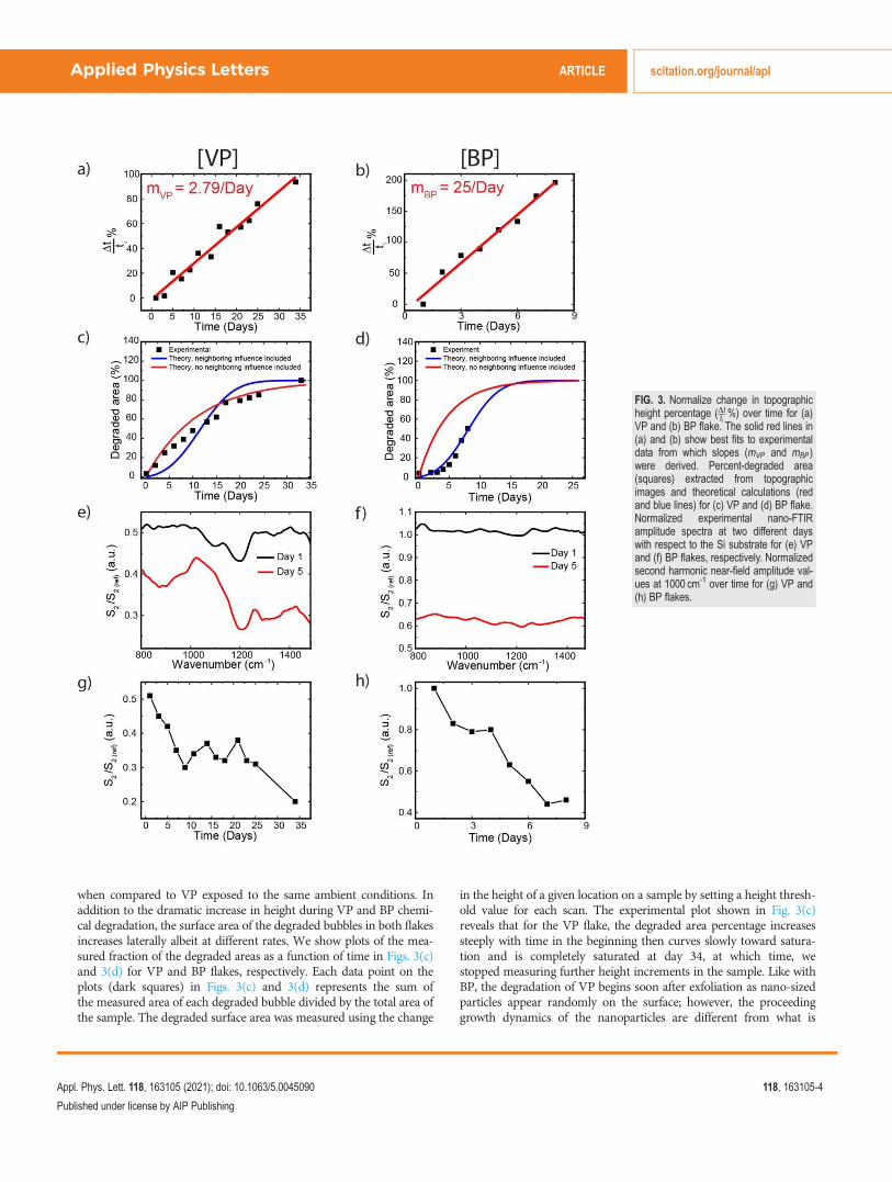
when compared to VP exposed to the same ambient conditions. Inaddition to the dramatic increase in height during VP and BP chemi-cal degradation, the surface area of the degraded bubbles in both flakesincreases laterally albeit at different rates. We show plots of the mea-sured fraction of the degraded areas as a function of time in Figs. 3(c)and 3(d) for VP and BP flakes, respectively. Each data point on theplots (dark squares) in Figs. 3(c) and 3(d) represents the sum ofthe measured area of each degraded bubble divided by the total area ofthe sample. The degraded surface area was measured using the change
in the height of a given location on a sample by setting a height thresh-old value for each scan. The experimental plot shown in Fig. 3(c)reveals that for the VP flake, the degraded area percentage increasessteeply with time in the beginning then curves slowly toward satura-tion and is completely saturated at day 34, at which time, westopped measuring further height increments in the sample. Like withBP, the degradation of VP begins soon after exfoliation as nano-sizedparticles appear randomly on the surface; however, the proceedinggrowth dynamics of the nanoparticles are different from what is
FIG. 3. Normalize change in topographicheight percentage (Dtti %) over time for (a)VP and (b) BP flake. The solid red lines in(a) and (b) show best fits to experimentaldata from which slopes (mVP and mBP )were derived. Percent-degraded area(squares) extracted from topographicimages and theoretical calculations (redand blue lines) for (c) VP and (d) BP flake.Normalized experimental nano-FTIRamplitude spectra at two different dayswith respect to the Si substrate for (e) VPand (f) BP flakes, respectively. Normalizedsecond harmonic near-field amplitude val-ues at 1000 cm-1 over time for (g) VP and(h) BP flakes.
Applied Physics Letters ARTICLE scitation.org/journal/apl
Appl. Phys. Lett. 118, 163105 (2021); doi: 10.1063/5.0045090 118, 163105-4
Published under license by AIP Publishing
observed in BP, as shown in Fig. 3(d) (also see Ref. 20). In BP, thedegraded area percentage change follows the sigmoid (S-shaped)growth curves, where the area percentage of the degraded regions ini-tially increases slowly then grows in an exponential fashion as particlesstart to coalesce covering the entire surface by day 15.20,21 Thedegraded area percentage differences between VP and BP may beexplained by different degradation processes as indicated in the phasespectra shown in Fig. 2. To qualitatively understand these differencesand the degradation process of VP, we use a variant of the forest-firemodel to fit our experimental data. The model is described in detail inRef. 20; briefly, the sample surface is divided in N�N square ele-ments, where each square can be either in an undegraded or degradedstate. We calculate the degradation probability after a small-time inter-
val Dt using Pn ¼ 1� e�Dt:g nð Þ; where gðnÞ is the degradation probabil-
ity per unit time of a surface element that has n degraded neighbors(0 � n � 8). Each degraded neighbor increases gðnÞ by a fixed amountDg, that is, gðnÞ ¼ gð0Þ þ nDg, where gð0Þ is the degradation probabil-ity per unit time. We note that this model gives a good fit to the VPexperimental data only if we neglect the influence of neighbors on thedegradation probabilities by setting Dg¼ 0, as shown by the red curvein Fig. 3(c). If, on the other hand, the influence of degraded neighborsis included, the model does not predict the experimentally observedresults [Fig. 3(c) blue curve]. The opposite scenario is true for BPwhere the model predicts the correct experimental behavior only if theinfluence of neighbors on the degradation probabilities is included asshown in Fig. 3(d) (also see Ref. 20). The model, thus, suggests, unlikeBP, the influence of degraded surface elements on non-degraded onesand does not contribute to the degradation process of VP.
The time-dependent IR near-field amplitude spectra provideinformation on real-time degradation changes of the real part of thelocal complex dielectric properties of the sample. Second harmonicnormalized nano-FTIR amplitude spectra of VP are shown in Fig. 3(e)taken at the point X in Fig. 2(c) at two different days. A similar plot forBP taken at the point Y in Fig. 2(d) is shown in Fig. 3(f). The normal-ized amplitude values decrease significantly over time as the samplesdegrade, which also complements the increasing topographic height inFigs. 3(a) and 3(b). Figures 3(g) and 3(h) show the second harmonicnormalized nano-FTIR amplitude spectra values extracted at1000 cm�1 from amplitude spectra for VP and BP, respectively, overtime. The decreasing normalized amplitude signal level, shown overseveral days in Figs. 3(g) and 3(h), is caused by continually decreasingpolarizability of the sample during degradation over time, and the effec-tive real-part of the dielectric functions is continuously decreasing forboth VP and BP flakes affecting the tip-sample near-field coupling.14–16
In summary, we have studied ambient degradation of CVD-synthesized VP in comparison with BP using Raman and nano-FTIRspectroscopy in the frequency range 800–1500 cm�1. VP Raman spec-tra are characterized by several peaks in the frequency range 100–300and 350–500 cm�1 including stretching and bending modes, angle dis-tortions, and rotational distortions. The nano-FTIR phase spectra ofVP and BP show broad peaks on top of a broad background resultingfrom a combination of many overlapping phosphorus oxides and
phosphoric acids species modes in the range of 850–1300 cm�1, whichincrease in intensity with time due to the degradation of the surface.Differences in the degradation spectra as well as thickness and permit-tivity changes between VP and BP indicate reduced oxygen insertionin VP, resulting in slower degradation compared to BP. VP is a vdWmaterial with promising electronic and photonic applications, and afundamental understanding of its properties and degradation processin comparison with other phosphorus allotropes will likely enable therealization of its full technological potential.
A.F. and Y.A. acknowledge support from the Air Force Officeof Scientific Research, Grant No. 426 No. FA9559-16-1-0172, andNational Science Foundation (CAREER), Grant No. 1553251. M.S.acknowledges support from the Air Force Office of ScientificResearch under Award No. FA9550-19RYCOR050.
DATA AVAILABILITY
The data that support the findings of this study are availablefrom the corresponding author upon reasonable request.
REFERENCES1P. W. Bridgman, J. Am. Chem. Soc. 38(3), 609 (1916).2R. Schuster, J. Trinckauf, C. Habenicht, M. Knupfer, and B. B€uchner, Phys.Rev. Lett. 115(2), 026404 (2015).
3H. Liu, Y. Du, Y. Deng, and P. D. Ye, Chem. Soc. Rev. 44(9), 2732 (2015).4Y. Abate, D. Akinwande, S. Gamage, H. Wang, M. Snure, N. Poudel, and S. B.Cronin, Adv. Mater. 30(29), 1704749 (2018).
5L. Li, Y. Yu, G. J. Ye, Q. Ge, X. Ou, H. Wu, D. Feng, X. H. Chen, and Y. Zhang,Nat. Nanotechnol. 9(5), 372 (2014).
6L. Zhang, H. Huang, B. Zhang, M. Gu, D. Zhao, X. Zhao, L. Li, J. Zhou, K. Wu,Y. Cheng, and J. Zhang, Angew. Chem., Int. Ed. 59(3), 1074 (2020).
7C. Gu, S. Zhao, J. L. Zhang, S. Sun, K. Yuan, Z. Hu, C. Han, Z. Ma, L. Wang, F.Huo, W. Huang, Z. Li, and W. Chen, ACS Nano 11(5), 4943 (2017).
8Y. Zhou, M. Zhang, Z. Guo, L. Miao, S.-T. Han, Z. Wang, X. Zhang, H. Zhang,and Z. Peng, Mater. Horiz. 4(6), 997 (2017).
9J. E. Padilha, A. Fazzio, and A. J. R. da Silva, Phys. Rev. Lett. 114(6), 066803(2015).
10H. Liu, A. T. Neal, Z. Zhu, Z. Luo, X. Xu, D. Tom�anek, and P. D. Ye, ACSNano 8(4), 4033 (2014).
11Z. Zhang, D.-H. Xing, J. Li, and Q. Yan, CrystEngComm 19(6), 905 (2017).12L. Zhang, M. Gu, L. Li, X. Zhao, C. Fu, T. Liu, X. Xu, Y. Cheng, and J. Zhang,Chem. Mater. 32(17), 7363 (2020).
13G. Fasol, M. Cardona, W. H€onle, and H. G. von Schnering, Solid StateCommun. 52(3), 307 (1984).
14F. Huth, A. Govyadinov, S. Amarie, W. Nuansing, F. Keilmann, and R.Hillenbrand, Nano Lett 12(8), 3973 (2012).
15J. M. Stiegler, Y. Abate, A. Cvitkovic, Y. E. Romanyuk, A. J. Huber, S. R. Leone,and R. Hillenbrand, ACS Nano 5(8), 6494 (2011).
16A. Fali, S. Gamage, M. Howard, T. G. Folland, N. A. Mahadik, T. Tiwald, K.Bolotin, J. D. Caldwell, and Y. Abate, ACS Photonics 8, 175 (2020).
17D. E. C. Corbrjdge, J. Appl. Chem. 6, 456 (1956).18M. Lechs and G. Zundel, Can. J. Chem. 57, 487 (1979).19J. D. Wood, S. A. Wells, D. Jariwala, K.-S. Chen, E. Cho, V. K. Sangwan, X. Liu,L. J. Lauhon, T. J. Marks, and M. C. Hersam, Nano Lett 14(12), 6964 (2014).
20S. Gamage, Z. Li, V. S. Yakovlev, C. Lewis, H. Wang, S. B. Cronin, and Y.Abate, Adv. Mater. Interfaces 3(12), 1600121 (2016).
21S. Gamage, A. Fali, N. Aghamiri, L. Yang, P. D. Ye, and Y. Abate,Nanotechnology 28(26), 265201 (2017).
Applied Physics Letters ARTICLE scitation.org/journal/apl
Appl. Phys. Lett. 118, 163105 (2021); doi: 10.1063/5.0045090 118, 163105-5
Published under license by AIP Publishing
Related Documents


