KL5A71007 JPEG chip datasheet -- Kawatetsu LSI -- rev 1.4 99.12.2 1 Video Rate JPEG KL5A71007 datasheet revision 1.4 revision history rev 0.1 97.1.27 First Draft rev 0.2 97.3.13 Register re-defined. 80pin pitch changed. rev 0.2 a 97.6.25 AC-timing added rev 0.3 97.9.22 rev 1.0 98.4.24 Characteristics fixed rev 1.1 98.9.10 IDDS re-defined rev 1.2 99.1.19 add max data reg rev 1.3 99.7.22 add DHT notice rev 1.4 99.12.2 FBGA80 canceled Kawasaki Steel Corporation LSI division

Welcome message from author
This document is posted to help you gain knowledge. Please leave a comment to let me know what you think about it! Share it to your friends and learn new things together.
Transcript

KL5A71007 JPEG chip datasheet -- Kawatetsu LSI -- rev 1.4 99.12.2
1
Video Rate JPEG KL5A71007 datasheet
revision 1.4
revision historyrev 0.1 97.1.27 First Draftrev 0.2 97.3.13 Register re-defined.
80pin pitch changed.rev 0.2 a 97.6.25 AC-timing addedrev 0.3 97.9.22rev 1.0 98.4.24 Characteristics fixed
rev 1.1 98.9.10 IDDS re-defined rev 1.2 99.1.19 add max data reg rev 1.3 99.7.22 add DHT notice rev 1.4 99.12.2 FBGA80 canceled
Kawasaki Steel Corporation
LSI division

KL5A71007 JPEG chip datasheet -- Kawatetsu LSI -- rev 1.4 99.12.2
2
0)Contents
Chapter1) Introduction -- Product feature2) Specification overview3) Chip Functionality4) 80pin LQFP Pin Layout5) Signal Descriptions6) Registers7) Control and data process flow8) Electrical specifications - DC Characteristics9) Electrical specifications - AC Characteristics10) Typical System Configurations11) spec difference from KL5A7100612) 64pin LQFP Package usage guide 12.1) Functionality restriction 12.2) Pin Layout 12.3) Signal Description13) Package Specification14) Known Bug list15) Glossary16) Index -- terms in alphabetical order

KL5A71007 JPEG chip datasheet -- Kawatetsu LSI -- rev 1.4 99.12.2
3
1)Introduction -- Product feature
KL5A71007 LSI is Kawasaki LSI's one chip JPEG hardware solution, whichis enhanced its performance while maintaining the ease-of-use chipinterface its precedence KL5A71006A has. This new chip has 8 times fasterin operation than the previous chip.
KL5A71007 can process either JPEG baseline compression ordecompression by user setting. Although chip throughput deeply depends onthe system configuration, Kawasaki set the chip design goal as follows.
- Optimized peak image processing throughput is 32Mbytes/sec.
For YUV 4:2:2 sampling color space data, VGA size (640 pixel by 480 line)one frame data is compressed or decompressed in around 20.5 milli-secondby KL5A71007. For SXGA image (1,280 pixel by 1,024 line), this chip canproduce to or reproduced by the compressed data in around 83 ms.
Both quantization table (Q-Table) and Huffman table (H-Table) are storedin on-chip RAMs. User can easily build up the table with writing table data,whose data entry sequence is very similar to that of JPEG DQT and DHTmarker format.
KL5A71007 can produce to or re-produce image from the compressed data,which complies ISO/IEC 10918-1 JPEG standard baseline process.
In addition to produce the bit stream data, KL5A71007 can handle JPEGheader information, RST marker generation/decode by itself.
KL5A71007 has several data transfer modes, which expands the flexibilityof system configuration.
--------- calculus example -----------------------------For VGA processing time
VGA image data volume = (640 x 480)pixel/frame x 2bytes/pixel = 614.4 kbytes /frame
Suppose the chip's peak throughput is 32Mbytes/sectotal time to compress or decompress = 614.4 k /(32M) sec = 19.2 ms/frame
By adding 1.3ms due to initialization and some overhead,we will get 20.5 ms for VGA size YUV 4:2:2 one frame processing.
Based on the same consideration, we can get 81.92 ms for 2,621.44 kbytedata. With 1.1ms margin, the chip will take 83ms to process SVGA sizeYUV 4:2:2 one frame data.

KL5A71007 JPEG chip datasheet -- Kawatetsu LSI -- rev 1.4 99.12.2
4
For pixel data transfer, user can select one of the following mode. - PCLK synchronous mode (thru pixel bus) - pixel DMA dedicated mode (thru pixel bus) - pixel DMA timesharing mode (thru host bus) - register access mode (thru host bus)
For code data transfer, either mode can be selected. - host DMA mode (thru host bus) - register access mode (thru host bus)
When choosing PCLK synch mode or pixel DMA dedicated mode, pixel datacan be transferred in parallel with code data transfer. Both transfer uses theseparated bus and user can make full use of the system hardware resources.
When using pixel DMA timesharing mode or register access mode, useraccesses both pixel and code data through host bus.
User can select bus size (16bit or 8bit), endian (big or little) of pixel bus andhost bus separately by setting the internal register bits.
Please note that pixel data is assumed to be transferred in block interleavedformat. Number of components and relative sampling ratio are userselectable within JPEG baseline specification.
To reduce the power consumption in idle mode, user can stop the chipinternal clock by asserting the external LOWPWR pin. Chip goes into lowpower mode.
Chip is molded into the thin flat package LQFP with 0.5mm lead pitch.There are two types of LQFP package depending on user application.For full use of KL5A71007 JPEG function, LQFP-80 (80pin, 12mm-sq moldsize) is the best choice. Another selection is LQFP-64, which is smaller(10mm-sq mold size).For LQFP-64, the PLL function is not available and the width of pixel bus isrestricted to 8 bits to save the pin count.

KL5A71007 JPEG chip datasheet -- Kawatetsu LSI -- rev 1.4 99.12.2
5
2)Specification overview
KL5A71007 is designed under the following specification.
a) compress/decompress method- compliant with the JPEG standard baseline process4
(ISO/IEC 10918-1)
b) digital imaging data format - each component has 8 bit data. - endian selectable - block interleaved format5
- unsigned or binary offset to be converted 2's compliment - data is level shifted (-128) internally
c) chip throughput - max 32M bytes/sec at internal clock rate 32MHz
d) marker code to be processed - for compressionSOI, DHT, DQT, DRI, SOF0, SOS, RSTm, EOI markers are generated andattached as header information.
- for decompressionSOI, DHT, DQT, DRI, SOF0, SOS, RSTm, EOI, DNL markers are decodedand used for data processing.
APPn followed by Lp bytes and COM followed by Lc bytes are completelyignored by the chip.
e) quantization table - 4 sets of programmable table area (RAM, up to 4 components)
f) Huffman table - 4 sets of programmable table area (RAM, 2 for DC table and 2 for AC table)
g) table setting- programmed by CPU through host interface or by reading the header data.- header data can be used during compression- data without table information can be decompressed by using pre- setting table data

KL5A71007 JPEG chip datasheet -- Kawatetsu LSI -- rev 1.4 99.12.2
6
h) input/output bus - pixel bus Used at PCLK synchronous mode and pixel DMA dedicated mode. Bus width is 8bits for LQFP-64 and 8bits/16bits selectable for LQFP-80.
- host bus Used for code data transfer at register access mode or host DMA mode. Also used for pixel data transfer at register access mode or pixel DMA timesharing mode.
i) input/output buffer - LVTTL compatible buffer. j) power voltage - 3.3 volt +/- 0.3 volt
l) clock rate - internal clock rate max 32 MHz - external clock rate max 32 MHz (PLL no use) max 16 MHz (PLL use)
m) low power mode - stop the internal clock
------------4) JPEG baseline processThe basic feature of the JPEG baseline process is summarizedas follows. (extracted from CCITT Rec. T.81 p.22)
- DCT-base process - image data8bits per component. Unsigned or binary offset.Input data is level shifted (-128) internally. - sequential coding (All components are coded into one scan) - Huffman coding2AC and 2DC tables - Decoderup to 4 components can be processed - interleaved (Ns > 1) and non-interleaved (Ns = 1) scan
5) block interleaved formatInput data is grouped by component constructing block datawhich is corresponding to 8 by 8 pixel data. Then block datais interleaved. Each data in the block is sequentiallytransferred (from upper left to lower right).

KL5A71007 JPEG chip datasheet -- Kawatetsu LSI -- rev 1.4 99.12.2
7
3)Chip interface and reset operation
internal block diagram
chip function overview
Data processing flow is as follows. In compress operation, pixel data in block interleaved format is fed in16Byte FIFO through PBUS interface from pixel bus or through HBUS IFfrom host bus. Pixel data is converted to DCT coefficients by DCT/IDCTblock. DCT coefficients are quantized by QTZ block, which use the quantizecoefficient stored in Q-table RAM. Quantized DCT coefficients are convertedto Huffman code by HE/HD block. Huffman code data is sent to 64ByteFIFO. With JPEG formatting (Marker attached), code data is out to the hostbusthrough HBUS IF. In decompress operation, JPEG code data is sent to 64Byte FIFO viaMarker Code Handler, where marker code is decoded and stripped. codedata is Huffman decoded, de-quantized and inversely transformed to thepixel data. Pixel data is sent to 16Byte FIFO and out to the pixel busthrough PBUS IF or to the host bus through HBUS IF. Both Quantization coefficients and Huffman codec information are storedin RAM, where values are programmable and are set at the beginning of theoperation by loading outside or extracting from the incoming JPEG data.
detail data transfer mode explanation
There are several mode to transfer the pixel and code data to/from outside.Four modes are presented for the pixel data transfer (a to d). Two modes (eand f) are shown for the code data transfer.
a) PCLK synchronous mode (thru pixel bus) - pixel transfer
FIFO
16B
PBUS
IF
Pixel BusQTZ
Q-tableRAM
HE
HD
H-tableRAM
FIFO
64B
MarkerCodeHandler
HBUSIF
Host Bus
PCLK syncronous
PDMAIndependence
Register accessPDMA time sharingHDMA
Functional block diagram
DCT
IDCT

KL5A71007 JPEG chip datasheet -- Kawatetsu LSI -- rev 1.4 99.12.2
8
With external PCLK, the pixel data is sent or received from the JPEG chipthrough pixel bus. Bus width can be changed 8bit (default) to 16bit bysetting the internal register value. For 8bit operation, PCLK is used as theinternal clock. For 16bit operation, internal PLL generates double frequencyof PCLK, which is used as internal clock and the pixel data can be accessedcontinuously. Incoming or outgoing pixel data can be holded by VALID andHOLD handshake. Pixel data sender can stop sending data by negatingVALID. Pixel data receiver can hold the incoming data by asserting HOLDsignal. Both operation can be performed independently each other. Directionof pixel bus is determined by the flags in mode register (HADDR = h06).After the hardreset, pixel bus is set to the input direction.
b) pixel DMA dedicated mode (thru pixel bus) - pixel transfer
Pixel bus can also be used as DMA bus. As slave DMA device, pixel datacan be transferred with PREQ and PACK handshake. DMA transfer is an asynchronous, which means no need to synchronizeboth pixel data and PACK signal with external chip clock. Both bus widthand endian format can be selected by setting the bus format register(HADDR = h00). Internal clock is also selectable by using PLL as externalclock doubler or by using the external clock itself.
c) pixel DMA timesharing mode (thru host bus) - pixel transfer
Instead of using pixel bus, host bus can be used in pixel data DMAtransfer. This is one of the host bus timesharing operation. Pixel data istransferred to the 16bit FIFO automatically in the chip. Pixel data DMAtransfer through host bus is performed by PREQ and PACK handshake.User also can use HRDN and HWRN control signals in cope with PACK byselecting the flag of mode register (HADDR = h06). Bus width, it's endianformat and internal clock generation method are the same as the descriptionin b).
d) register access mode (thru host bus) - pixel transfer
Pixel data can be transferred by using the register access mode through hostbus in timesharing operation. External controller drives the pixel dataregister address (HADDR = h2E), asserts the control signal - HRDN orHWRN and transfers the pixel data. Transaction is not ended untilasserting the HRDY signal by JPEG chip.This HRDN/HWRN - HRDY handshake is exactly the same as that of JPEG

KL5A71007 JPEG chip datasheet -- Kawatetsu LSI -- rev 1.4 99.12.2
9
chip internal register access. To assure the correct operation, HRDYassertion is always verified by the external controller before the terminationof transaction each time. It is strongly recommended that the externalcontroller checks the status register (HADDR = h30) every time beforeaccessing the pixel data register to see the pixel data is available or not.Otherwise the deadlock might occur because JPEG chip requires the codedata to proceed the operation while the external controller is waiting for theending of the pixel data transfer, which will never end due to the internalbuffer full or empty.
e) host DMA mode (thru host bus) - code transfer
Code data can be transferred by using host DMA mode through the hostbus. Handshake is HREQ and HACK. As is the pixel DMA timesharingmode, HRDN or HWRN control or just HACK control is user selectable bychoosing the mode register (HADDR = h06). DMA transfer is the asynchronous to the external clock. The host buswidth and endian format are set by the flag of the corresponding internalregister. For internal clock generation, please refer to the description in b).
f) register access mode (thru host bus) - code transfer
Code date also can be transferred by using the register access mode. Itsregister address is h2C (code data register).Treatment of HRDY and the method to avoid the deadlock described in pixeldata transfer using register access mode section are also true here. Pleaserefer to d) for detail discussion.
soft-reset operation
In addition to be reset by the external reset pin, the chip can be reset bysetting the register bit with register access. This operation is called "soft-reset". The register address of thecorresponding register flag is h24. Please note that the data in the systemregisters is NOT cleared by the soft-reset operation.
lowpower operation
To save the power consumption when the chip is not in operation, externallowpower pin is useful. By pulling the LOWPWR pin to L, internal clock isstopped and the chip goes into the lowpower mode. It is stronglyrecommended to avoid lowpower setting during compress or decompress

KL5A71007 JPEG chip datasheet -- Kawatetsu LSI -- rev 1.4 99.12.2
10
operation. When releasing the LOWPWR pin to H, the chip is recoveredfrom the lowpower mode. Before doing the compress or decompressoperation, soft-reset operation is required.
If internal PLL function is used by setting the MODE pins to an appropriatevalue, 2 msec lock-time is needed after the release of LOWPWR pin toguarantee the PLL lock-time. Then softreset is expected before starting thecompress or decompress operation.

KL5A71007 JPEG chip datasheet -- Kawatetsu LSI -- rev 1.4 99.12.2
11
4)80pin LQFP Pin Layout(LQFP‐80)
4.1 Functional Signal Grouping
4.2 Pin Assignments(Top view)
Vdd3 Gnd3Vdd3 Gnd3
Functional Signal Grouping (LQFP-80)
16 PDAT[15:0]PREQPAC
LP_OUTLP_INRESETNLOWPWRPLL_TCLKMODE[2:0]TEST[1:0]
166
Pixel Bus (22) Host Bus (29)
Others (10)
PCLKVALIDHOLFSYNC
Vdd3 Gnd4
HADR[5:0]
HDAT[15:0]HCSNHRDYHRDNHWRNHREQHACKHIRQ
TOP VIEW
TE
ST
LO
WP
WR
VD
D
GN
D
LP
_IN
LP
_OU
T
PC
LK
PL
L_V
DD
PL
L_G
ND
GN
D
GN
D
RE
SE
TN
MO
DE
0
MO
DE
1
HIR
Q
HD
AT
15
HD
AT
14
HD
AT
13
HD
AT
12
GN
D
Index
PDAT5
VDD
PDAT2
PDAT3
GND
PDAT4
PDAT6
PDAT7
VALID
HOLD
VDD
PDAT14
PDAT1
FSYNC
TEST
PLL_TCLK
PACK
PREQ
PDAT0
PDAT15
VDD
HADR5
PDAT9
PDAT8
HDAT0
HDAT1
HDAT2
HDAT3
HDAT4
GND
HDAT5
HDAT6
HDAT7
HDAT8
HDAT9
HDAT10
HDAT11
GND
MODE2
VDD
GN
D
HC
SN
HR
DN
HW
RN
HR
DY
HR
EQ
PD
AT
13
PD
AT
12
GN
D
GN
D
GN
D
PD
AT
11
PD
AT
10
HA
CK
HA
DR
0
HA
DR
1
HA
DR
2
HA
DR
3
HA
DR
4
VD
D
1 2021
4060 41
61
80

KL5A71007 JPEG chip datasheet -- Kawatetsu LSI -- rev 1.4 99.12.2
12
5) Signal Descriptions(LQFP-80)
No. Signal Pin I/O Function∗ Host Bus
1 HADR[5:0]39,
42-46I
The HADR[5:0] are "Host Bus Address"signals and provide internal registeraddress.
2 HDAT[15:0]16-19,24-30,32-36
I/O
The HDAT[15:0] are "Host Bus Data"signals and used for transferring internalregister data, compressed data, and pixeldata in time sharing DMA mode andregister access mode. Data bus width can be selected 16 bits(word transferring) or 8 bits (bytetransferring) by internal register, which isset 8 bits after hard reset. In word transfer, endian format also canbe selected by internal register, which is setlittle endian format after hard reset. LSB isHDAT[0].
3 HCSN 59 I
The HCSN is "Host Bus Chip Select" andactive low signal. When asserted,KL5A71007 recognizes as register accessmode.
4 HRDY 56 OT
The HRDY is "Host Bus Ready" and activehigh signal. When asserted, it indicates the end of datawriting or the permission of data reading.It is driven while HCSN is asserted.
5 HRDN 58 I
The HRDN is "Host Bus Read Strobe" andactive low signal. When asserted, reading operation isexecuted. In register access mode, HDATare read at HRDY asserted timing. In Host Bus DMA mode without HRDNand HWRN, please connect to L.
6 HWRN 57 I
The HWRN is "Host Bus Write Strobe" andactive low signal. When asserted, writing operation isexecuted. In register access mode, HDATare written at HRDY asserted timing. In Host Bus DMA mode without HRDNand HWRN, please connect to L.
7 HREQ 55 O
The HREQ is "Host Bus DMA Request" andactive high signal after hard reset. In Host Bus DMA mode, HREQ is assertedwhen data transfer is permitted, andrequires DMA access. The Active level can be selected by internalregister.
8 HACK 47 I
The HACK is "Host Bus DMA Acknowledg-ment" and active high signal after hardreset. When asserted, KL5A71007 negatesHREQ. In Host Bus DMA mode withoutHRDN and HWRN, transfer is executed byHACK only. The active level can be selected by internalregister.

KL5A71007 JPEG chip datasheet -- Kawatetsu LSI -- rev 1.4 99.12.2
13
5)Signal Descriptions(LQFP‐80)
No. Signal Pin I/O Function∗ Host Bus
9 HIRQ 15 O
The HIRQ is "Host Bus InterruptionRequest" and active high signal after hardreset. When the event occurs which ismonitored by permission bits of IRQ flagregister, KL5A71007 sets IRQ flag bitsand asserts HIRQ. After reading the IRQ register or reset,the flag bits are cleared and HIRQ isnegated. In reset, permission bits arealso cleared. The active level can be selected byinternal register.
∗ Pixel Bus
10 PDAT[15:0]
63-62,54-53,49-48,38-37,74-71,69-66
I/O
The PDAT[15:0] are "Pixel Data Bus"signals and used for transferring pixeldata in PCLK synchronous mode andindividual DMA mode. Data bus width can be selected 16 bits or8 bits by internal register, which is set 8bits after hard reset. In word transfer, endian format also canbe selected by internal register, which isset little endian format after hard reset. In byte transfer, please connect upperbyte to H or L. Or in time sharing DMAmode and register access mode, pleaseconnect PDAT to H orL. LSB is PDAT[0].
11 PCLK 4 I
The PCLK is "System Clock" signal. KL5A71007 operates according to thisclock. In PCLK synchronous mode, Pixeldata is processed by every PCLK. WhenLOWPWR is H, internal clock is stoppedand KL5A71007 enters low power modeeven though PCLK is given.
12 VALID 75 I/O
The VALID is "PDAT Valid" and activehigh signal. In PCLK Synchronous mode,It is asserted by output side of PDAT andindicates that PDAT are valid. Except for PCLK Synchronous mode,please connect to L.
13 HOLD 76 I/O
The HOLD is "PDAT Hold" and activehigh signal. In PCLK Synchronous mode, It isasserted by input side of PDAT andindicates that PDAT can not be received.After negated, PDAT transferis resumed. Except for PCLK Synchronous mode,please connect to L.

KL5A71007 JPEG chip datasheet -- Kawatetsu LSI -- rev 1.4 99.12.2
14
5)Signal Descriptions(LQFP‐80)
No. Signal Pin I/O Function∗ Pixel Bus
14 FSYNC 77 I/O
The FSYNC is "PCLK SynchronousTransfer Period" and active high signal. In PCLK Synchronous mode, It isasserted from first data transfer to lastdata transfer by output side of PDAT andindicates that PDAT are transferred. Except for PCLK Synchronous mode,please connect to L.
15 PREQ 65 O
The PREQ is "Pixel Bus DMA Request"and active high signal after hard reset. In Pixel Bus DMA mode both timesharing and individual, PREQ is assertedwhen data transfer is permitted, andrequires DMA access. The active level can be selected byinternal register.
16 PACK 64 I
The PACK is "Pixel Bus DMAAcknowledg-ment" and active high signalafter hard reset. When asserted, KL5A71007 negatesPREQ. In Pixel Data DMA mode both timesharing and individual, DMA transfer isexecuted by PACK The active level can be selected byinternal register.
∗ Others
17 LOWPWR 8 I
The LOWPWR is "Low Power ModeTrigger" and active high signal. When LOWPWR is asserted, internalsystem clock is stopped and power issaved. After negated, please execute soft reset.
18 RESETN 12 I
The RESETN is "Hard Reset", and activelow signal. When RESETN is asserted, all registersare cleared and KL5A71007 returns initialstate, and all bi-directional pins and 3-state outputs become Hi-Z. RESETN also works same operations inlow power mode. The difference between hard reset andsoft reset is soft rest does not clear theregisters except for Error Report.

KL5A71007 JPEG chip datasheet -- Kawatetsu LSI -- rev 1.4 99.12.2
15
5)Signal Descriptions(LQFP‐80)
No. Signal Pin I/O Function∗ Others
19 MODE[2:0]22,
14-13I
The MODE[2:0] are "Chip Mode Control"signals.
o b101 using PLLo b001 not using PLL
If PLL is available, please input L toMODE[2] until power become stable. Afterthat, please input H to MODE[2]. The locktime for PLL is 2ms.
20 TEST[1:0] 7,78 IThe TEST is "Test Mode Control" signal.Please connect to GND.
21 LP_IN 2 I
22 LP_OUT 3 O
The LP_IN and LP_OUT are "Off-ChipLoop Filter Pin for PLL". If internal PLL is available, off-chip loopfilter is needed to remove the high-frequency noise element as shown Fig. 5.1.Otherwise, please connect LP_IN to GND,and open LP_OUT.
23 PLL_TCLK 79 IPLL_TCLK is "PLL Test Clock". Pleaseconnect to GND.
24 PLL_VDD 5 VDDPLL_VDD is "PLL Power Supply". Pleaseconnect to VDD.
25 PLL_GND 6 GNDPLL_GND is "PLL Ground supply". Pleaseconnect to GND.
Low pass filter diagram Filter constant recommendation
Fig. 5.1 Off-chip Loop Filter diagram
R1
R2
C
LP_OUT LP_IN
No. items value unit
1
2
3
R1
R2
C
20 kΩ
75 kΩ
0.01 µF

KL5A71007 JPEG chip datasheet -- Kawatetsu LSI -- rev 1.4 99.12.2
16
6)Registers
The definitions of internal registers are indicated below. After hardreset, the registers are set up the (def) value. If there is no (def) shown, theregisters are cleared to 0. In soft reset, the registers do not changed exceptfor Error Report Register which is cleared to (def). If the (def) value or once set up value is used, resetting is not needed.However resetting Huffman table is needed when DHT marker code isrequired in every compressed data.
No.RegisterName
HADR[5:0]
fieldbit
Function bitdefinition
Function bit definition
∗ Interface Set Up Register0 Host Bus Width 1:16bit 0:8bit(def)
1Host Bus Endian
Format1:Big 0:Little(def)
2 Pixel Bus Width 1:16bit 0:8bit(def)Bus Mode[3:0] h00
3Pixel Bus Endian
Format1:Big 0:Little(def)1
Note:In LQFP-64 package, [3:2] are ignored because Pixel Bus is 8 bits. If bit [0] is 1, even and odd register are joined. In that case, Endian Format is followed by bit [1]. For Endian Format, see 7.8.
0 HREQ active level 1:assert H(def) 0:assert L1 HACK active level 1:assert H(def) 0:assert L2 PREQ active level 1:assert H(def) 0:assert L3 PACK active level 1:assert H(def) 0:assert L
2Signal Active Level[4:0]
h02
4 HIRQ active level 1:assert H(def) 0:assert L3 PDATuse [0] h04 0 PDAT use 1:use 0:not use(def)
∗ Initial Set Up Register
0Compression/
Decompression1:Compression(def)0:Decompression
1Header Informa-
tion Loading1:by Registers(def)0:by JPEG Header
2Compressed Data
Output Enable1:enable(def)0:disable
4-3Compressed Data
Transfer Mode
0,1:Register Access(def 0)2:DMA(with HRDN and HWRN)3:DMA(without HRDN and HWRN)
ModeSpecify[6:0]
h06
6-5Pixel Data
Transfer Mode
0:Register Access(def)1:PCLKSynchronous2,3:DMA
4
Note: Pixel Data Transfer Mode PDAT use[0] Mode Specify[6:5]Register Access bx h0PCLK Synchronous bx h1
Individual DMA (PDAT use) b1 h2 or h3 Time Sharing DMA (PDAT not use) b0 h2 or h3(same as Mode Specify[4:3])

KL5A71007 JPEG chip datasheet -- Kawatetsu LSI -- rev 1.4 99.12.2
17
6)Registers
No.RegisterName
HADR[5:0]
fieldbit
Function bitdefinition
Function bit definition
∗ Initial Set Up Register
h08 7-0Lower Byte of
Limitunit is 1 K bytes(from 0 K bytes to 255 K bytes)
Limit OfCompressedData Volume[15:0](k bytes)
h09 7-0Upper Byte of
Limit
unit is 256 K bytes(from 0 K bytes to 64 M bytes)5
Note:In compression, If compressed data volume reaches this limit, KL5A71007 stopsoutputting HDAT but continues internal operation.After hard reset, they are cleared to 0, and then KL5A71007 does not stop outputting.
1-0 Output format0:normal(def) 1:normal2:only header 3:only ECS
2DHT Output
Enable1:enable(def) 0:disable
6CompressedDataFormat[3:0]
h0A
3DQT Output
Enable1:enable(def) 0:disable
∗ Table Set Up Register
7-0Table data transferby byte
H,Q table data set up by byteTable Data[7:0] (byte),[15:0] (word)<write only>
h1015-0
Table data transferby word
H,Q table data set up by word7
Note:DHT or DQT marker code segment is needed for input. In word access, if number of data byte is odd, the extra byte of last word data is ignored. Endian format is followed by internal register. These registers are not used except for table data setting up by register access mode.
∗ Header Information Registerh12 7-0 DRI lower byte DRI lower byte(7:0) (0:def)Restart
Interval[15:0] h13 7-0 DRI upper byte DRI upper byte(15:8) (0:def)8Note:When set up 0, DRI and RST markers are not added in compressed data.
h14 7-0Number of lines
lower byteNumber of lines lower byte(7:0) (0:def)
9Number of Lines(SOF;Y)[15:0] h15 7-0
Number of linesupper byte
Number of lines upper byte(15:8) (0:def)
h16 7-0Number of samplesper line lower byte
Number of samples per line lowerbyte (7:0) (1:def)
10
Number ofSamples PerLine (SOF;X)[15:0] h17 7-0
Number of samplesper line upper byte
Number of samples per line upperbyte (15:8) (0:def)
2-0No. of componentsin Frame (Nf)
Defined in 1(def) - 4
11
Number of ImageComponents(SOF;Nf,SOS;Ns)[15:0]
h185-3
No. of componentsin Scan (Ns)
Defined in 1(def) - 4

KL5A71007 JPEG chip datasheet -- Kawatetsu LSI -- rev 1.4 99.12.2
18
6) Registers
No.RegisterName
HADR[5:0]
fieldbit
Function bit definition Function bit definition
∗ Header Information Register
h1A 7-0Component identifier
C10-255(def 0)
1-0Horizontal Sampling
Factor H10:H1=4 1:H1=1(def)2:H1=2 3:H1=3
3-2Vertical Sampling
Factor V10:V1=4 1:V1=1(def)2:V1=2 3:V1=3
12
SOF 1stComponentInformation[13:0] h1B
5-4 Q table selector Tq1 0-3(def 0)
h1C 7-0Component identifier
C21-255(def 1)
1-0Horizontal Sampling
Factor H20:H1=4 1:H1=1(def)2:H1=2 3:H1=3
3-2Vertical Sampling
Factor V20:V1=4 1:V1=1(def)2:V1=2 3:V1=3
13
SOF 2ndComponentInformation[13:0] h1D
5-4 Q table selector Tq2 0-3(def 0)
h1E 7-0Component identifier
C32-255(def 2)
1-0Horizontal Sampling
Factor H30:H1=4 1:H1=1(def)2:H1=2 3:H1=3
3-2Vertical Sampling
Factor V30:V1=4 1:V1=1(def)2:V1=2 3:V1=3
14
SOF 3rdComponentInformation[13:0] h1F
5-4 Q table selector Tq3 0-3(def 0)
h20 7-0Component identifier
C43-255(def 3)
1-0Horizontal Sampling
Factor H40:H1=4 1:H1=1(def)2:H1=2 3:H1=3
3-2Vertical Sampling
Factor V40:V1=4 1:V1=1(def)2:V1=2 3:V1=3
15
SOF 4thComponentInformation[13:0] h21
5-4 Q table selector Tq4 0-3(def 0)

KL5A71007 JPEG chip datasheet -- Kawatetsu LSI -- rev 1.4 99.12.2
19
6)Registers
No. Register NameHADR[5:0]
fieldbit
Function bitdefinition
Function bit definition
∗ Header Information Register
1-0Scan component
selector Cs1
0:Cs1=C1(def)1:Cs1=C22:Cs1=C33:Cs1=C4
2DC table selector
Td10-1(def 0)
SOS 1stComponentInformation[3:0]
3AC table selector
Ta10-1(def 0)
5-4Scan component
selector Cs2
0:not allowed by JPEG spec1:Cs2=C2(def)2:Cs1=C33:Cs1=C4
6DC table selector
Td20-1(def 0)
SOS 2ndComponentInformation[7:4]
h22
7AC table selector
Ta20-1(def 0)
1-0Scan component
selector Cs3
0-1:not allowed by JPEG spec2:Cs3=C3(def)3:Cs3=C4
2DC table selector
Td30-1(def 0)
SOS 3rdComponentInformation[3:0]
3AC table selector
Ta30-1(def 0)
5-4Scan component
selector Cs40-2:not allowed by JPEG spec3:Cs4=C4(def)
6DC table selector
Td40-1(def 0)
16
SOS 4thComponentInformation[15:12]
h23
7AC table selector
Ta40-1(def 0)
∗ Control and Data Register
17 Soft Reset[0] h24 0 Soft reset command1:execute0:auto clear(def)
19
Compression/DecompressionStart Command[0]
h28 0 Start command1:execute0:auto clear(def)
20
Compression/DecompressionEndCommand[0]
h2A 0 End command1:execute0:auto clear(def)
7-0Compressed Datatransfer by byte
compressed data by byte21
CompressedData[7:0](byte),[15:0](word)
h2C15-0
Compressed Datatransfer by word
compressed data by word
7-0Pixel Data transfer
by bytepixel data by bytePixel Data
[7:0](byte),[15:0](word)
h2E15-0
Pixel Data transferby word
pixel data by word22
Note:This register is effective when pixel bus transfer is register access.

KL5A71007 JPEG chip datasheet -- Kawatetsu LSI -- rev 1.4 99.12.2
20
6)Registers
No.RegisterName
HADR[5:0]
fieldbit
Function bitdefinition
Function bit definition
∗ Report Register
0 Busy status 1:busy 0:idle(def)
1Compressed data
Access1:allowed 0:not(def)
2 Pixel data Access 1:allowed 0:not(def)23
Status[3:0](read only)
h30
3 Error status 1:error(see h36) 0:normal(def)
0 Data output ready 1:ready 0:flag reset(def)
1 Last data output end 1:end 0:flag reset(def)
2Overflow
compressed datalimit
1:overflow 0:flag reset(def)
3 Error occur 1:error 0:flag reset(def)
4 Permission for bit[0] 1:permit 0:not(def)
5 Permission for bit[1] 1:permit 0:not(def)
6 Permission for bit[2] 1:permit 0:not(def)
IRQ Flag[7:0](read only [3:0])
h32
7 Permission for bit[3] 1:permit 0:not(def)
24
Note: If upper bits [7:4] are set, KL5A71007 sets [3:0] flags and asserts HIRQ whencorresponding events is occurred. If [7:4] are 0, KL5A71007 does not set [3:0] flags andassert HIRQ. After hard reset, IRQ flag and HIRQ are cleared. Lower bits [3:0] are read-only. They and HIRQ are cleared after IRQ Flag register read automatically. To confirmthe overflow from the limit of compressed data volume, setting bit [6] is needed.
h34 7-0Compressed datavolume lower byte
less than 256kB, 1kB step(The 10th-17th power of two)
CompressedData Volume [15:0](kbytes,read only) h35 7-0
Compressed datavolume upper byte
Less than 64MB, 256kB step(The 18th-25th power of two)
h3E 7-0Compressed datavolume lower byte
less than 256B, 1B step(The 0th-7th power of two)
25CompressedData Volume [15:0](bytes,read only) h3F 1-0
Compressed datavolume upper byte
Less than 1kB, 256B step(The 8th-9th power of two)
ErrorReport[7:0](read only)
h36 7-0
Error report(All error occurs in
decompressionexcept h1)
h0:no errors(def)h1:overflow from the limit of compressed data volume (Compression)h2:restart interval differ from DRIh4:mismatch component ID between SOS and SOFh8:number of blocks per MCU is more than 11h10:header parameter does not match JPEG baseline standardh20:marker segment length errorh40:unknown marker codeh80:huffman decode error
26
Note:When error is occurred, the corresponding flag is set 1. If Error report is between h2and h80, KL5A71007 can not operate any more. In this case, initializing by hard or softreset is needed to recover. If Error Report is not h0, Status Register [3] is set 1. Thisregister is cleared after reading, or hard reset and soft reset.

KL5A71007 JPEG chip datasheet -- Kawatetsu LSI -- rev 1.4 99.12.2
21
7) Control and data process flow
7.1 Power On
After power on, hard reset is needed. And then, please establish"Interface Set Up registers" from Host Bus by register access mode. Thevalue of system registers is not cleared by soft reset but hard reset. In case of using PLL, please connect MODE[2] pin to L at power on, andconnect H after power become stable. Next, please execute soft reset after2ms lock time.
7.2 How To Establish "Initial Set Up Registers"
Firstly, to establish 'Mode Specify' register (address:h06) is needed fordesignation of operation and transferring way. Some examples are shownbelow.
Pixel bus Host bus SR04[0] SR06[6:3]a) PCLK synchronous DMA with HRDN, HWRN b1 b6b) Individual DMA DMA with HRDN, HWRN b1 hAc) Time sharing DMA DMA without HRDN, HWRN b0 hFd) register access register access b0 h0
To set up 'Mode Specify' register is also needed to determine compression ordecompression, and data output enable in compression.And to set up 'Compressed Data Format' register (address:h0A) is needed todetermine compressed data output format, and output enable of tableinformation.
'Limit Of Compressed Data Volume' registers (address:h09,h08) are neededto determine the limit of output data volume in compression. The unit isK byte. If data volume is over this limit, KL5A71007 stops outputting andcontinues internal compress operation. The right data volume is registeredin 'Compressed Data Volume' register (address:h35,h34) whether thevolume is over the limit or not.

KL5A71007 JPEG chip datasheet -- Kawatetsu LSI -- rev 1.4 99.12.2
22
7.3 How To Establish "Table Data"
For establishing table data, writing table data to 'Table Data' register(address:h10) is needed, except for establishing by compressed data withtable data. DHT and DQT marker code segment is required for writtendata. KL5A71007 checks the table definition length. When define theHaffman table, the register address h06 and h0A must be fixed. In compression, if table data is required in each compressed data, tabledata have to be set up in every flame compression. For only table data, continuative writing mode which can transfer pluraldata during one HCSN asserted period, can be used.
7.4 Set up the Header informationBefore compression, write the header information to the register in
register access mode. The address is from h12 to h18 and h1A to h23.Compression is done with this information.
If set the value except 0 to the register h12 and h13, the restart intervalmaker (RST) will add to the compressed data.
In de-compression mode, header information is set to these registers.
7.5 CompressionThis section describes the compression operation with setting up described
in 7.2 to 7.4. This chip will start operation when set the Start Register(register h28). If change the registers after starting the operation, This chipwill not operate correctly. Register information can be read during theoperation, so the status or IRQ information can be checked.
After starting this chip, the header data will be output. Read the data withasserting the HACK signal after the HREQ signal is asserted in HOST-DMA mode. In register access mode, read data from the compression dataregister (register address = h2C) after confirming the access flag can beaccessed of the compression data of the status register (register address =h30).
When the output of the header data is completed, writing the pixel databecomes possible. In the PCLK synchronous mode after confirming theHOLD signal negated, assert FSYNC and VALID, and write the pixeldata. In pixel DMA mode, after confirming the PREQ signal is assertedwrite the pixel data with assert the PACK signal. Write the image data inthe image data register (register address = h2E) for the register access modeafter confirming being able to access the register by reading the statusregister (register address = h30).
The output of the compression data starts from the host bus after about180-240CLK after beginning writing the pixel data. Latency changesaccording to whether the access mode and the pixel data are continuouslywritten. The access method is the same as the case of the output of theheader data.
KL5A71007 JPEG chip datasheet -- Kawatetsu LSI -- rev 1.4 99.12.2
23
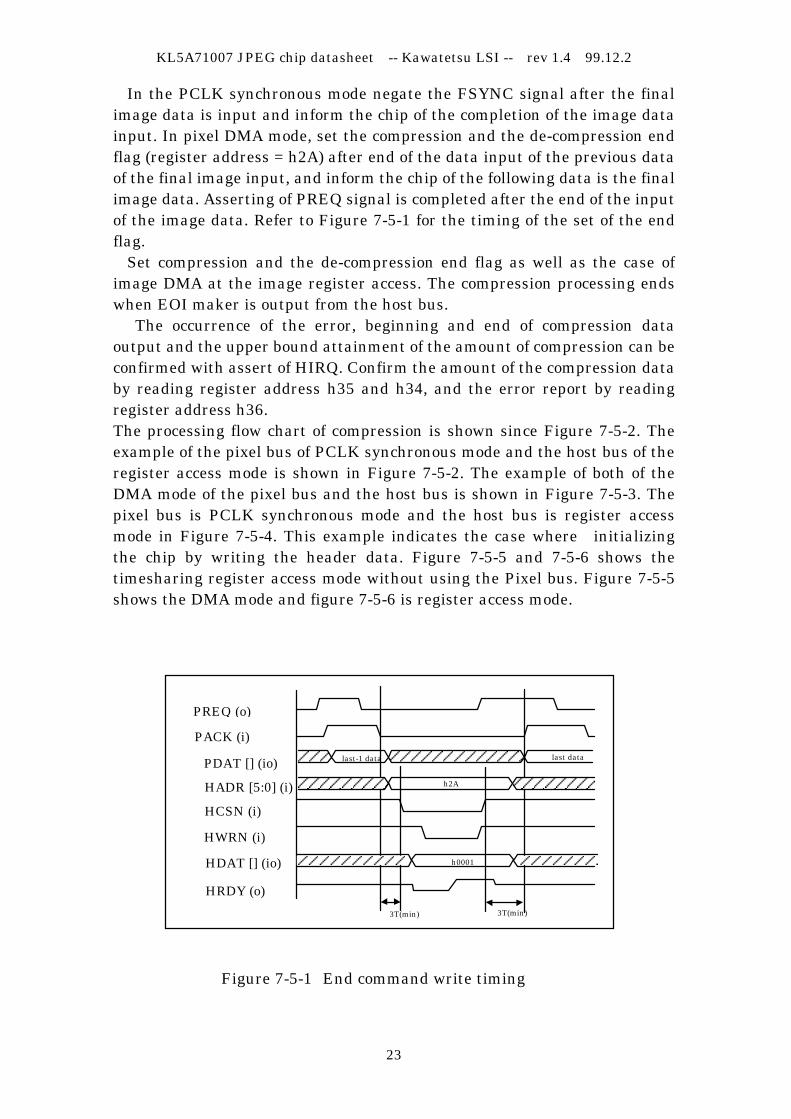
In the PCLK synchronous mode negate the FSYNC signal after the finalimage data is input and inform the chip of the completion of the image datainput. In pixel DMA mode, set the compression and the de-compression endflag (register address = h2A) after end of the data input of the previous dataof the final image input, and inform the chip of the following data is the finalimage data. Asserting of PREQ signal is completed after the end of the inputof the image data. Refer to Figure 7-5-1 for the timing of the set of the endflag.
Set compression and the de-compression end flag as well as the case ofimage DMA at the image register access. The compression processing endswhen EOI maker is output from the host bus.
The occurrence of the error, beginning and end of compression dataoutput and the upper bound attainment of the amount of compression can beconfirmed with assert of HIRQ. Confirm the amount of the compression databy reading register address h35 and h34, and the error report by readingregister address h36.The processing flow chart of compression is shown since Figure 7-5-2. Theexample of the pixel bus of PCLK synchronous mode and the host bus of theregister access mode is shown in Figure 7-5-2. The example of both of theDMA mode of the pixel bus and the host bus is shown in Figure 7-5-3. Thepixel bus is PCLK synchronous mode and the host bus is register accessmode in Figure 7-5-4. This example indicates the case where initializingthe chip by writing the header data. Figure 7-5-5 and 7-5-6 shows thetimesharing register access mode without using the Pixel bus. Figure 7-5-5shows the DMA mode and figure 7-5-6 is register access mode.
Figure 7-5-1 End command write timing
PDAT [] (io)
PACK (i)
PREQ (o)
last-1 data last data
HRDY (o)
HDAT [] (io)
HWRN (i)
HCSN (i)
HADR [5:0] (i) h2A
h0001
3T(min) 3T(min)

KL5A71007 JPEG chip datasheet -- Kawatetsu LSI -- rev 1.4 99.12.2
24
7)Control and data process flow
7.5 Compression(continued)
Figure 7-5-2 Register access, PCLK synchronous mode compression flow
start
reset
Start command
End ofCompressed data?
ReadingCompressed
End
Set registersand Table
Enable toaccess compressed data?
yes
yes
no
Writing theregister andthe tabledata
Writing thecontrolregister
Accesee to statusregister
ReadingData register
RegisterAccess mode
∗ Host Bus:Register access mode∗ Pixel Bus : PCLK synchronous mode
no
HOLD=H ?
FSYNC assert
yes
no
Holdingpixel data
yes
no
FSYNC negate
End of pixel data
Last pixeldata ?
Pixel datainput
Accesee to statusregister orIRQ assert

KL5A71007 JPEG chip datasheet -- Kawatetsu LSI -- rev 1.4 99.12.2
25
7)Control and data process flow
7.5 compression(continued)
Figure 7-5-3 Host DMA, Pixel DMA compression flow
start
reset
HREQ=H?
Start command
End ofCompressed data
ReadCompressed data
end
Set Registersand Table
yes
yes
no
Write theRegister andThe tabledata
Write theControlregister
Check the HREQ
ReadData register
RegisterAccess mode
∗ Host Bus : DMA mode∗ Pixel Bus : DMA mode(HREQ,PREQ:assert H)
DMA mode
RegisterAccess mode
Access to statusRegister orIRQ assert
PREQ=H?
yes
no
WritePixel data
yes
no Pixel data=last-1?
End command
no
PREQ=H?
Write Pixel data
yes
no
End of pixel data

KL5A71007 JPEG chip datasheet -- Kawatetsu LSI -- rev 1.4 99.12.2
26
7)Control and data process flow
7.5 Compression(continued)
Figure 7-5-4 Initialize flow by Header data
start
reset
Start command
end
Set registers
yes
no
Write toControl register
RegisterAccess mode
Register access
Start command
End ofCompresed data?
ReadCompressed data
Enable toAccess compress Data?
yes
yes
no
Read and write toThe registers
Write to theControl registers
Access toStatus register
ReadData register
Confirm the end ofheader input by readThe status register
Confirm the end ofcompressed data byaccess the statusregister or the IRQ
∗ Host Bus : Register access mode and Setting from header data∗ Pixel Bus : PCLK synchronous mode
HOLD=H?
FSYNC assert
yes
no
Hold thePixel data
yes
no
FSYNC negate
End of pixel data
Last pixelData?
Write header
End ofHeader input?
no
Input thePixel data
Write toData register

KL5A71007 JPEG chip datasheet -- Kawatetsu LSI -- rev 1.4 99.12.2
27
7)Control and data process flow
7.5 compression(continued)
Figure 7-5-5 Time sharing DMA mode compression flow
start
reset
HREQ=H?
Start command
End ofCompressed data?
Read compressed data
End
Set registersAnd table
yes
yes
no
Write registersAnd table
Write toControl register
Confirm theHREQ,PREQ
Read and writedata
RegisterAccess mode
∗ Host Bus : Time sharing DMA mode(compressed data,pixel data)(HREQ,PREQ:assert H)
∗ Pixel Bus : not used
DMA mode
RegisterAccess mode
Confirm the end ofCompression by readstatus register orIRQ
PREQ=H?
yes
no
WritePixel data
yes
no Pixel data=last-1?
End command(Host bus,registeraccess mode)
no

KL5A71007 JPEG chip datasheet -- Kawatetsu LSI -- rev 1.4 99.12.2
28
7)Control and data process flow
7.5 Compression(continued)
Figure 7-5-6 Time sharing register access mode compression flow
start
reset
Start command
End ofCompressed data?
ReadCompressed
End
Set registersAnd table
Enable toAccess Compressed data?
yes
yes
no
Write registerAnd table
Write toControl register
Access toStatus register
Write and readData register
RegisterAccess mode
∗ Host Bus : Time sharing register access Mode(compressed data,pixel data)∗ Pixel Bus : not used
Confirm statusRegister or IRQ
no
yes
no
WritePixel data
yes
no Pixel data=last-1?
End command(Host Bus,registeraccess)
Enable toAccess Pixel data?

KL5A71007 JPEG chip datasheet -- Kawatetsu LSI -- rev 1.4 99.12.2
29
7)Control and data process flow7.6 Data Format
The compressed data is output by the data format in accordance with theJPEG standard. Figure 7-6-1 shows the data format. In mode of withouttable data in the header or without using the restart maker, the data formatbecomes data which deletes the item which is each correspondence from thisfigure.Figure 7-6-2 shows the example of the compression data. Please refer toJPEG standard (ISO/IEC10918-1) for detailed information on the dataformat.
Compressed data format
SOI(Start Of Image):Marks the beginning of data. Code value=hFFD8 EOI(End Of Image) :Marks the end of data. Code value=hFFD9
Huffman table data
DHT(16):Marks the beginning of Huffman table data. Code value=hFFC4 Lh(16) :Number of byte in data except DHT. Tc(4) :DC table=0、AC table=1. Th(4) :Table number Ln(8) :Huffman table data for Th. Specifies the number of Huffman Codes for each length. Vij(8) :Huffman table data for Th. The elements In occurrence frequency of the order. (DC=SSSS,AC=RRRR/SSSS)
*( )The number indicates the size(bits)
Fig.7-6-1 Compressed data format
SOI Quantization table dataHuffman table data
Frame header Scan header Compressed data EOI
DRI
DHT Lh Tc Th
L1 L16 V16,L16……………L2 V1, 1 V1, 2 …………
BITS HUFFVAL1byte

KL5A71007 JPEG chip datasheet -- Kawatetsu LSI -- rev 1.4 99.12.2
30
7)Control and data process flow7.6 Data format(continued)
Quantization table data
DQT(16):Marks the beginning of quantization table. Code value=hFFDB Lq(16) :Number of byte in data except DQT. Pq(4) :Specifies the precision of table data. The value is 0 (8bit,baseline). Tq(4) :Table number Qn(8) :Specifies the nth element out of 64 elements.
DRI
DRI(16) :Marks the beginning of DRI. Code value=hFFDD Lr(16) :Number of byte in data except DRI. Ri(8) :The number of MCU in the restart interval.
Frame header
SOF(16) :Marks the beginning of the Frame header. Code value in the baseline = hFFC0 Lf(16) :Number of byte in data except SOF. P(8) :Precision in bits for pixel data. Value in baseline = 8 Y(16) :Number of line in frame. X(16) :Number of samples per line. Nf(8) :Number of image components in frame. Cn(8) :Component identifier Hn(4) :Horizontal sampling factor Vn(4) :Vertical sampling factor Tqn(8) :Quantization table selector
*( )The number indicates the size(bits)
Fig.7-6-1 Compressed data format(continued)
DQT Lq Pq Tq Q0 Q1 Q63…………
DRI Lr Ri
SOF Lf P Y X Nf
C1 TqnH1 V1 Tq1 ………… Cn VnHn

KL5A71007 JPEG chip datasheet -- Kawatetsu LSI -- rev 1.4 99.12.2
31
7)Control and data process flow
7.6 Data format(continued)
Scan header
SOS(16) :Marks the beginning of the Scan header. Code value = hFFDA Ls(16) :Number of byte in data except SOS. Ns(8) :Number of image components in scan. Csn(8) :Scan component selector Tdn(4) :DC Huffman table selector Tan(4) :AC Huffman table selector Ss(8) :Start of spectral selector. The value in baseline is 0. Se(8) :End of spectral selector. The value in baseline is d63(h3F). Ah(4) :The value in baseline process is 0. Al(4) :The value in baseline process is 0.
*( )The number indicates the size(bits)
Fig.7-6-1 Compressed data format(continued)
SOS Ls Ns Cs1 CsnTd1Ta1 ………… TdnTan Ss Se Ah Al

KL5A71007 JPEG chip datasheet -- Kawatetsu LSI -- rev 1.4 99.12.2
32
7)Control and data process flow
7.6 Data format(continued) This is the example of the compressed data. Our chip generate the headerin this order.
Fig.7-6-2 Compressed data example
number of thenecessary table isrepeated.
number of thenecessary table isrepeated.
Lq Pq Tq
Q0 Q1 Q63…………
SOI
DQT
FF D8
FF DB 00 43 0 0
DHT Lh Tc Th
L1 L16 V16,L16…………L2 V1 1 V1,2 …………
BITS HUFFVA
FF C4 00 1F 0 1
SOF Lf P Y X Nf
C1 Tq 3H1 V 1 Tq1 C3 V3H3
SOS Ls Ns Cs1 Cs3Td 1Ta 1 Td3Ta 3 Ss Se Ah Al
FF C0 00 11 0 8 01 E0 02 D0 03
00 2 1 00
C2 H2 V2 Tq 2
01 1 1 01 02 1 1 01
FF DA 00 0C 03 00 01 020 0
Cs 2 Td2Ta 2
1 1 1 1 00 3F 0 0
ECS
EOI
FF D9
::
::
DRI Lr Ri
FF DD 00 04 00 28

KL5A71007 JPEG chip datasheet -- Kawatetsu LSI -- rev 1.4 99.12.2
33
7)Control and data process flow
7.7 De-compression This section describes the de-compression operation with setting updescribed in 7.2 to 7.4. This chip will start operation when set the StartRegister (register h28). If change the registers after starting the operation,This chip will not operate correctly. Register information can be read duringthe operation, so the status or IRQ information can be checked. After starting this chip, the header data will be input. Write the data withasserting the HACK signal after the HREQ signal is asserted in HOST-DMA mode. In register accesses mode, write data to the compressed dataregister (register address = h2C) after confirming the access flag of thestatus register (register address = h30).
Write the compressed data after the header data, then pixel data will beoutput after 200-600 clock period. Latency changes according to whether theaccess mode and the compressed data are continuously written. In PCLKsynchronous mode, the pixel data is output after asserting the FSYNCsignal. In pixel DMA mode, after confirming the asserting the PREQ signaland read the pixel data with asserting the PACK signal. Read the imagedata from the image data register (register address = h2E) for the registeraccess mode after confirming being able to access the register by reading thestatus register (register address = h30). In host DMA mode, set the compression and the de-compression end flag(register address = h2A) after end of the data input of the previous data ofthe final compressed data input, and inform the chip the following data isthe final compressed data. Then input the EOI code as the last data. HREQsignal is asserted after writing the last data if the end flag is not set. HREQis negated because this chip decode EOI maker and acknowledges the end ofthe compression data. There is no problem if input the HREQ after the EOIcode because this chip disregards the data after EOI. Refer to Figure 7-5-1for the timing of the set of the end flag. In the PCLK synchronous mode, after the output of the last pixel data,this chip negate the FSYNC signal and tell the completion of the output ofthe pixel data. In the pixel DMA mode, this chip end the asserting the PREQsignal after the last pixel data. In the register access mode of the compressed data, set the end flag forcompletion of the data. If the end flag is not set, disregards the asserting theaccess flag. This chip knows the end of the input of the compressed data byrecognizing the EOI maker. The data access flag is negated at this timing.Because data input after the EOI marker is ignored, there is no stateproblem same as DMA mode. The occurrence of the error and the start of the image data output,completion can be confirmed with assert of HIRQ by setting of the IRQ flag(register address =h32). To confirm the de-compression result read the errorreport register, address =h36.

KL5A71007 JPEG chip datasheet -- Kawatetsu LSI -- rev 1.4 99.12.2
34
7)Control and data process flow
7.7 De-compression(continued)Flow figure of de-compression is shown in the following. As for the figure
7-7-1, pixel side is when the PCLK synchronous mode, a host side is theregister access mode. A figure 7-7-2 is the example of the DMA mode in bothpixel side and the host side. A figure 7-7-3, a figure 7-7-4 are when eitherpixel bus isn't used and a host bus is used in the time sharing mode. Figure7-7-3 is DMA, a figure 7-7-4 is register access mode.
Fig.7-7-1 Register access, PCLK synchronous de-compression flow
∗ Host Bus : register access mode∗ Pixel Bus : PCLK synchronous mode
start
reset
Start command
End of compressed Data input
Write register
Write compresseddata
Enable toAccess data?
yes
no Access toStatus register
Write compresseddataTo data register
Register accessmode
External control orAccess to register
Write toControl register
End ofCompressed
data?yes
no
End
FSYNC=L
yes
no
Access toPixel data
FSYNC=H?
yes
no
VALID=H?
yes
no
Write to register

KL5A71007 JPEG chip datasheet -- Kawatetsu LSI -- rev 1.4 99.12.2
35
7)Control and data process flow
7.7 De-compression(continued)
Fig.7-7-2 Host DMA、Pixel DMA de-compression flow
∗ Host Bus : DMA mode∗ Pixel Bus : DMA mode(HREQ,PREQ:assert H)
start
reset
Start command
End of compressed Data input
Set register Write register
Write toControl register
Register accessmode
Compressed data=last-1?
Write data
HREQ=H?
yes
no
yes
no
Write toControl register
End
End ofDe-compression?
Read Pixel data
yes
no
PREQ=H?
yes
no Confirm theHREQ
Write data
DMA mode
End command
HREQ=H?
Write last data
HREQ signal assert
Write last data
Confirm the end ofde-compression bystatus register orIRQ
DMA mode
RegisterAccess mode
Register accessmode
no
yes

KL5A71007 JPEG chip datasheet -- Kawatetsu LSI -- rev 1.4 99.12.2
36
7)Control and data process flow
7.7 De-compression(continued)
Fig.7-7-3 Time sharing DMA de-compression flow
start
reset
HREQ=H?
Start command
Compressed data=last-1?
Write compressed data
End
Set registersAnd table
yes
yes
no
Write registerAnd table
Write toControl register
Confirm HREQand PREQ
Write and readdata
Register accessmode
∗ Host Bus :Time sharing DMA mode(Compressed data,Pixel data)(HREQ,PREQ:assert H)
∗ Pixel Bus : not used
DMA mode
Register accessmode
PREQ=H?
yes
no
Read pixel data
yes
no End ofPixel data?
End command
no
Confirm the end ofde-compression bystatus register orIRQ

KL5A71007 JPEG chip datasheet -- Kawatetsu LSI -- rev 1.4 99.12.2
37
7)Control and data process flow
7.7 De-compression(continued)
Fig.7-7-4 Time sharing register access de-compression flow
start
reset
Start command
End ofPixel data?
WriteCompressed data
End
Set registers
Enable to Accesscompessed data?
yes
yes
no
Wrte toregister
Write toControl register
Access toStatus register
Write and readData register
RegisterAccess mode
∗ Host Bus: Time sharing register access mode (compressed data,pixel data)∗ Pixel Bus : not used
Confim the statusregister or IRQ
no
Enable to Access Pixel data?
yes
no
ReadPixel data

KL5A71007 JPEG chip datasheet -- Kawatetsu LSI -- rev 1.4 99.12.2
38
7)Control and data process flow
7.8 In data of the order A host, a pixel bus can set up the Endian form of the data in the case of thedata access by 16 bits in each of the independence. An Endian form is eightbits in word-data arrangement form (1 byte). Little Endian arranges loweraddress data in the byte mode on the lower byte, upper address data on theupper byte. That is reverse with Big Endian. An example in data of the orderwith Big Endian, Little Endian is shown in the following. It is shown withthe example with Header (SOI, DQT) by the comparison with eight bits.
Little Endian
16bit 8bit MSB LSB MSB LSB
Dataorder
hex (bin)
Dataorder
hex (bin)1
2
3
D8 FF (1101 1000 1111 111)
DB FF (1101 1011 1111 1111)
43 00 (0100 0011 0000 0000)
123456
FF (1111 1111)D8 (1101 1000)FF (1111 1111)DB (1101 1011)00 (0000 0000)43 (0100 0011)
Table 7-8-1 Little Endian data order
Big Endian
16bit 8bit MSB LSB MSB LSB
Dataorder
hex (bin)
Dataorder
hex (bin)1
2
3
FF D8 (1111 111 1101 1000)
FF DB (1111 1111 1101 1011)
00 43 (0000 0000 0100 0011)
123456
FF (1111 1111)D8 (1101 1000)FF (1111 1111)DB (1101 1011)00 (0000 0000)43 (0100 0011)
Table 7-8-2 Big Endian data order

KL5A71007 JPEG chip datasheet -- Kawatetsu LSI -- rev 1.4 99.12.2
39
7)Control and data process flow
7.9 Examples of setting up registers
Pixel data : YUV4:2:2, 640x480 pixelcompressed data : Interchange formatHost Bus : 16 bits little endianPixel Bus : 16 bits little endianBus Access : Host DMA mode, Pixel individual DMA modeActive level : HREQ, HACK, PREQ, PACK and HIRQ are active H.Data Volume Limit : 256 K bytesRestart Interval : 40 MCUDQT identifier : Y=0, UV=1DHT identifier : Y=0, UV=1HIRQ assert condition : last data output end, overflow compressed
data limit, error occur
Address(hex)
Value Function
00020406
080A121416181A1C1E22
32
0005001F00010057
0100000C002801E00280001B0600150115020ED0
00E0
Bus definition is 16 bits and little endian.HREQ, HACK, PREQ, PACK and HIRQ are active H.PDAT useDMA mode, data output enable, header information loading byregisters, compressionthe limit of compressed data volume is 256 K bytesnormal output, with DHT and DQTDRI=40MCUY=480 linesX=640 pixels per lineNf=Ns=3 componentsTq1=0, H1=2, V1=1, C1=0Tq2=1, H2=1, V2=1, C2=1Tq3=1, H3=1, V3=1, C3=2Cs1=C1, Td1=Ta1=0Cs2=C2, Td2=Ta2=1Cs3=C3, Td3=Ta3=1HIRQ is asserted when last data output end, overflow compresseddata limit, error occur.
Table 7-9-1 An example of setting up registers in compression

KL5A71007 JPEG chip datasheet -- Kawatetsu LSI -- rev 1.4 99.12.2
40
7)Control and data process flow
7.9 Examples of setting up registers
Address(hex)
Value Function
00020406
32
0005001F00010056
00E0
Bus definition is 16 bits and little endian.HREQ, HACK, PREQ, PACK and HIRQ are active H.PDAT useDMA mode, data output enable, header information loading byregisters, decompressionHIRQ is asserted when last data output end, overflow compresseddata limit, error occur.
# In decompression, most parameters are loaded by header of compresseddata.
Table 7-9-2 An example of setting up registers in decompression

KL5A71007 JPEG chip datasheet -- Kawatetsu LSI -- rev 1.4 99.12.2
41
7)Control and data process flow
7.10 Outlines of frame operation time
Outlines of flame operation time are indicated below. The flame size is640x480 pixels and the format is YUV4:2:2. "T" means system clock period.The value shown in a parenthesis is time in case 32 MHz system clock rate.In this examples, Pixel Bus is 16 bits width and accessed by PCLKsynchronous mode, and Host Bus is 16 bits width and accessed by DMAmode, and There are no interruptions from external systems. Input oroutput time for header can be changed by header parameters for examplenumber of tables.
Fig.7-10-1 frame operation time example
compresion
header output pixel data input
compressed data output
1800T(56µs)
1500T
(47µs)
200T
(6µs)
614,400T(19.2ms)
total time is 19.3 ms
de-compresion
initialset up
header input compressed data input
pixel data output
40T
(1.3µs)
1500T
(47µs)
600T
(19µs)
total time is 19.3ms
614,400T(19.2ms)

KL5A71007 JPEG chip datasheet -- Kawatetsu LSI -- rev 1.4 99.12.2
42
8) Electrical Characteristics (DC)
8.1 Absolute Maximum Ratings
No. Parameter Symbol Limit Unit1 DC Supply Voltage VDD -0.3 - +0.4 V2 Input Voltage VIN -0.3 - VDD+0.3 V3 DC Output Current IOUT ±15 mA4 Storage Temperature TSTG -55 - +125 °C
8.2 Recommended Operating Conditions
No. Parameter Symbol Limit Unit5 DC Supply Voltage VDD 3.0 - 3.6 V6 Ambient Temperature Ta 0 - +70 °C
8.3 DC Characteristics (under Recommended Operating Conditions)
No. Parameter Symbol Test Condition Min Max Unit7 Input Low Voltage VIL ― 0.8 V8 Input High Voltage VIH 2.0 3.9 V9 Output Low Voltage VOL IOL = +4mA ― 0.4 V10 Output High Voltage VOH IOL = -4mA 2.4 ― V11 Input Leakage Current IIL VIN = GND -10 ― µA12 Input Leakage Current IIH VIN = VDD ― 10 µA13 Output Leakage Current IOZ At 3-state Output -10 10 µA
14Quiescent Supply Current
IDDSVIN = VDD or GND
― 100 µA
15 Dynamic Supply Current IDDOPOutput Capacitance
= 50pF &Internal f =32MHz
― 140 mA
― 1.2 mA16
Supply Current at LOWPWR
IDDLPLOWPWR = H
VIN = VDD or GND(except PCLK) 850(typical) µA
17 Input Capacitance CINf = 1MHz,
VIN = GND,v in = 100 mVrms
― 15 PF
18 Output Capacitance COUT ― 15 PF

KL5A71007 JPEG chip datasheet -- Kawatetsu LSI -- rev 1.4 99.12.2
43
9)Electrical Characteristics (AC)
9.1 PCLK The maximum frequency at PCLK input using PLL is the half of not usingPLL. Even if PLL is in use or not, the maximum through-put is the same.Because Internal PCLK signal is made twice as fast as PCLK input in thecase of using PLL.
Figure 9-1-1 PCLK timings
Symbol Parameter Min Max Unit Conditions31.25 - ns PLL is not in use.
t1 PCLK Cycle Time62.5 83 ns PLL is in use.15 - ns PLL is not in use.
t2PCLK Pulse WidthHigh 30 42 ns PLL is in use.
15 - ns PLL is not in use.t3 PCLK Pulse Width Low
30 42 ns PLL is in use.- Lock Time - 2 ms PLL is in use.
Table 9-1-2 AC Characteristics-PCLK input
PCLK (i) t2
t1
t3

KL5A71007 JPEG chip datasheet -- Kawatetsu LSI -- rev 1.4 99.12.2
44
9.2 Host Bus register access mode (write)
Figure 9-2-1 Host Bus (register access) write timing
Symbol Parameter Min Max Unit Conditionst1 HCSN Write Cycle 6T - ns
t2HADR Setup Time (HWRNFall)
-12 - ns *1
t3HADR Hold Time (HWRNFall)
3T - ns
t4 HCSN Negate Width 1.5T - ns
t5HCSN Hold Time (HRDYRise)
0 - ns
t6HWRN Hold Time (HRDYRise)
0 - ns
t7 HWRN Negate Width 1.5T - ns
t8HDAT Setup Time (HWRNFall)
-12 - ns *2
t9HDAT Hold Time (HRDYRise)
0 - ns
t11HCSN Assert - HRDY LOutput Delay
- 18 ns Output Loading is 50pF.
t12 If both HCSN and HWRN are asserted, WRITE cycle will begin.
t12a HCSN Assert - HRDY Assert - 3.5T ns Output Loading is 50pF.t12b HWRN Assert - HRDY Assert - 3.5T ns Output Loading is 50pF.
t13HCSN Negate - HRDY 3-StateDelay
- 18 ns Output Loading is 50pF.
Note: *1 A valid data delay on HADR is admitted 12ns from assert of HWRN.
*2 A valid data delay on HDAT is admitted 12ns from assert of HWRN.
Table 9-2-2 AC Characteristics-Host Bus (register access) write mode
HRDN(i)
HRDY(o)
HDAT [] (io)
HWRN(i)
HCSN(i)
HADR [5:0](i)
t3
t2
t11t12b
valid
t12a
t8 t9
t5
t6
t4
t7
t13
valid
t1
valid valid

KL5A71007 JPEG chip datasheet -- Kawatetsu LSI -- rev 1.4 99.12.2
45
9.3 Host Bus register access mode (read)
Figure 9-3-1 Host Bus (register access) read timing
Symbol Parameter Min Max Unit Conditionst1 HCSN Read Cycle 6T - nst2 HADR Setup Time (HRDN Fall) -12 - ns *1t3 HADR Hold Time (HRDN Fall) 3T - nst4 HCSN Negate Width 1.5T - nst5 HCSN Hold Time (HRDY Rise) 0 - nst6 HRDN Hold Time (HRDY Rise) 0 - nst7 HRDN Negate Width 0.5T - nst8 If both HCSN and HRDN are asserted, HDAT will be on output state.
t8aHCSN Assert - HDAT OutputDelay
- 18 ns Output Loading is 50pF.
t8bHRDN Assert - HDAT OutputDelay
- 18 ns Output Loading is 50pF.
t9HRDY Assert - HDAT Valid DataOutput Delay
- 5 ns Output Loading is 50pF.
t10 If HCSN or HRDN is negated, HDAT will be on 3-state.
t10aHCSN Negate - HDAT 3-stateDelay
- 18 ns Output Loading is 50pF.
t10bHRDN Negate - HDAT 3-stateDelay
- 18 ns Output Loading is 50pF.
t11HCSN Assert - HRDY L Output Delay
- 18 ns Output Loading is 50pF.
t12 If both HCSN and HRDN are asserted, READ cycle will begin.t12a HCSN Assert - HRDY Assert - 3.5T ns Output Loading is 50pF.t12b HRDN Assert - HRDY Assert - 3.5T ns Output Loading is 50pF.
t13HCSN Negate - HRDY 3-StateDelay
- 18 ns Output Loading is 50pF.
Note: *1 A valid data delay on HADR is admitted 12ns from assert of HRDN.
Table 9-3-2 AC Characteristics-Host Bus (register access) read mode
HWRN(i)
HRDY(o)
HDAT [](io)
HRDN(i)
HCSN(i)
HADR [5:0](i)
valid
t3
t2
t11t12b
valid
t12a
t8at8b t9
t5
t6
t10a
t10b
t4
t7
t13
valid
valid
t1

KL5A71007 JPEG chip datasheet -- Kawatetsu LSI -- rev 1.4 99.12.2
46
9.4 Host Bus register access (writing the table data continually) mode
In Host Bus register access (writing the table data continually) mode,admitted write data is only table data. For the mode specification, pleaseuse the table data address (h10), then other writing for specification withother address is not necessary. In other mode, Host Bus register access isthe usual writing sequence (show 9.2). The table data address is write onlybut not readable.
Figure 9-4-1 Host Bus register access (writing the table data continually)timing
Symbol Parameter Min Max Unit Conditionst1 HWRN Write Cycle 4T - nst2 HADR Setup Time (HWRN Fall) -12 - ns *1t3 HADR Hold Time (HWRN Fall) 3T - nst4 HCSN Negate Width 1.5T - nst5 HCSN Hold Time (HRDY Rise) 0 - nst6 HWRN Hold Time (HRDY Rise) 0 - nst7 HWRN Negate Width 1.5T - nst8 HDAT Setup Time (HWRN Fall) -12 - ns *2t9 HDAT Hold Time (HRDY Rise) 0 - ns
t11HCSN Assert - HRDY L OutputDelay
- -18 ns Output Loading is 50pF.
t12 If both HCSN and HWRN are asserted, WRITE cycle will begin.t12a HCSN Assert - HRDY Assert - 3.5T ns Output Loading is 50pF.t12b HWRN Assert - HRDY Assert - 3.5T ns Output Loading is 50pF.
t13HCSN Negate - HRDY 3-StateDelay
- 18 ns Output Loading is 50pF.
Note: *1 A valid data delay on HADR is admitted 12ns from assert of HWRN.
*2 A valid data delay on HDAT is admitted 12ns from assert HWRN.
Table 9-4-2 AC Characteristics-Host Bus register access (writing the tabledata continually) mode
HRDN(i)
HRDY(o)
HDAT [](io)
HWRN(i)
HCSN(i)
HADR [5:0](i)t3t2
t11t12b
valid
t12a
t8 t9
t5
t6
t13
t1
valid valid
valid
t7
valid

KL5A71007 JPEG chip datasheet -- Kawatetsu LSI -- rev 1.4 99.12.2
47
9.5 Host Bus DMA mode (the compression controlled by HWRN andHRDN)
Figure 9-5-1 Host Bus DMA timing (the compression controlled by HWRNand HRDN)
Symbol Parameter Min Max Unit Conditionst1 PREQ Assert - PACK Assert 0 - nst2 PACK Assert - PREQ Negate 0.5T 2.5T ns Output Loading is 50pF.t3 PACK Assert Width 2T - nst4 PACK Negate - PREQ Assert 2T - ns Output Loading is 50pF.t5 HWRN Setup Time (PACK Assert) 0 - nst6 HWRN Hold Time (PACK Negate) 0 - nst7 HWRN Assert Width 2T - nst8 HWRN Negate Width 2T - nst9 HDAT Setup Time (HWRN Assert) -12 - ns *1t10 HDAT Hold Time (HWRN Negate) 0 - nst11 HREQ Assert - HACK Assert 0 - nst12 HACK Assert - HREQ Negate 0.5T 2.5T ns Output Loading is 50pF.t13 HACK Assert Width 2T - nst14 HACK Negate - HREQ Assert 2T - ns Output Loading is 50pF.t15 HRDN Setup Time (HACK Assert) 0 - nst16 HRDN Hold Time (HACK Negate) 0 - nst17 HRDN Assert Width 2T - nst18 HRDN Negate Width 2T - ns
t19HRDN Assert - HDAT OutputDelay
- 18 nsWhen Compression Dataare out. Output Loadingis 50pF.
t20HRDN Negate - HDAT 3-stateDelay
- 18 nsWhen Compression Dataare out. Output Loadingis 50pF.
Note: *1 A valid data delay on HDAT is admitted 12ns from assert of HWRN.
Table 9-5-2 AC characteristics-Host Bus DMA mode (the compressioncontrolled by HWRN and HRDN)
HWRN(i)
HDAT [15:0](io) valid
t1
t5
t7
t6
t8
HRDN(i)
HACK(i)
HREQ(o)
t17
t18t21
t16
t10t9t20
valid
PACK(i)
PREQ(o)t2 t4
t11t12 t14
valid
t19
valid
t15
t3
t13

KL5A71007 JPEG chip datasheet -- Kawatetsu LSI -- rev 1.4 99.12.2
48
9.6 Host Bus DMA mode (the compression controlled by HACK and PACK)
Figure 9-6-1 Host Bus DMA timing (the compression controlled by HACKand PACK)
Symbol Parameter Min Max Unit Conditionst1 PREQ Assert - PACK Assert 0 - nst2 PACK Assert - PREQ Negate 0.5T 2.5T ns Output Loading is 50pF.t3 PACK Assert Width 2T - nst4 PACK Negate - PREQ Assert 2T - ns Output Loading is 50pF.
t5HDAT Setup Time (PACKAssert)
-12 - ns *1
t6HDAT Hold Time (PACKNegate)
0 - ns
t7 PACK Negate - HACK Assert 2T - nst8 HREQ Assert - HACK Assert 0 - nst9 HACK Assert - HREQ Negate 0.5T 2.5T ns Output Loading is 50pF.t10 HACK Assert Width 2T - nst11 HACK Negate - HREQ Assert 2T - ns Output Loading is 50pF.
t12HACK Assert - HDAT OutputDelay
- 18 nsWhen Compression Dataare out. Output Loadingis 50pF.
t13HACK Negate - HDAT 3-stateDelay
- 18 nsWhen Compression Dataare out. Output Loadingis 50pF.
Note: *1 A valid data delay on HDAT is admitted 12ns from assert of PACK.
Table 9-6-2 AC characteristics-Host Bus DMA mode (the compressioncontrolled by HACK and PACK)
t13
t8t9
HDAT [15:0](io) valid
t1
HACK(i)
HREQ(o)
t6t5 t12
valid
PACK(i)
PREQ(o)t2 t4
t10
valid
t11
valid
t7
t3

KL5A71007 JPEG chip datasheet -- Kawatetsu LSI -- rev 1.4 99.12.2
49
9.7 Host Bus DMA mode (the decompression controlled by HWRN andHRDN)
Figure 9-7-1 Host Bus DMA timing (the decompression controlled by HWRNand HRDN)
Symbol Parameter Min Max Unit Conditionst1 PREQ Assert - PACK Assert 0 - nst2 PACK Assert - PREQ Negate 0.5T 2.5T ns Output Loading is 50pF.t3 PACK Assert Width 2T - nst4 PACK Negate - PREQ Assert 2T - ns Output Loading is 50pF.t5 HRDN Setup Time (PACK Assert) 0 - nst6 HRDN Hold Time (PACK Negate) 0 - nst7 HRDN Assert Width 2T - nst8 HRDN Negate Width 2T - ns
t9 HRDN Assert - HDAT Output Delay - 18 nsWhen Pixel Data are out.Output Loading is 50pF.
t10HRDN Negate - HDAT 3-stateDelay
- 18 nsWhen Pixel Data are out.Output Loading is 50pF.
t11 HREQ Assert - HACK Assert 0 - nst12 HACK Assert - HREQ Negate 0.5T 2.5T ns Output Loading is 50pF.t13 HACK Assert Width 2T - nst14 HACK Negate - HREQ Assert 2T - ns Output Loading is 50pF.t15 HWRN Setup Time (HACK Assert) 0 - nst16 HWRN Hold Time (HACK Negate) 0 - nst17 HWRN Assert Width 2T - nst18 HWRN Negate Width 2T - nst19 HDAT Setup Time (HWRN Assert) -12 - ns *1t20 HDAT Hold Time (HWRN Negate) 0 - ns
Note: *1 A valid data delay on HDAT is admitted 12ns from assert of HWRN.
Table 9-7-2 AC characteristics-Host Bus DMA mode (the decompressioncontrolled by HWRN and HRDN)
HWRN(i)
HDAT [15:0](io) valid
t1
t5
t7
t6
t8
HRDN(i)
HACK(i)
HREQ(o)
t17
t18t21
t16
t10t9t20
valid
PACK(i)
PREQ(o)t2 t4
t11t12 t14
valid
t19
valid
t15
t3
t13

KL5A71007 JPEG chip datasheet -- Kawatetsu LSI -- rev 1.4 99.12.2
50
9.8 Host Bus DMA mode (the decompression controlled by HACK andPACK)
Figure 9-8-1 Host Bus DMA timing (the decompression controlled by HACKand PACK)
Symbol Parameter Min Max Unit Conditionst1 PREQ Assert - PACK Assert 0 - nst2 PACK Assert - PREQ Negate 0.5T 2.5T ns Output Loading is 50pF.t3 PACK Assert Width 2T - nst4 PACK Negate - PREQ Assert 2T - ns Output Loading is 50pF.
t5PACK Assert - HDAT OutputDelay
- 18 nsWhen Pixel Data are out.Output Loading is 50pF.
t6PACK Negate - HDAT 3-stateDelay
- 18 nsWhen Pixel Data are out.Output Loading is 50pF.
t7 PACK Negate - HACK Assert 2T - nst8 HREQ Assert - HACK Assert 0 - nst9 HACK Assert - HREQ Negate 0.5T 2.5T ns Output Loading is 50pF.t10 HACK Assert Width 2T - nst11 HACK Negate - HREQ Assert 2T - ns Output Loading is 50pF.
t12HDAT Setup Time (HACKAssert)
-12 - ns *1
t13HDAT Hold Time (HACKNegate)
0 - ns
Note: *1 A valid data delay on HDAT is admitted 12ns from assert of HACK.
Table 9-8-2 AC characteristics-Host Bus DMA mode (the decompressioncontrolled by HACK and PACK)
t13
t8t9
HDAT [15:0](io) valid
t1
HACK(i)
HREQ(o)
t6t5 t12
valid
PACK(i)
PREQ(o)t2 t4
t10
valid
t11
valid
t7
t3

KL5A71007 JPEG chip datasheet -- Kawatetsu LSI -- rev 1.4 99.12.2
51
9.9 Pixel Bus DMA mode (write)
Figure 9-9-1 Pixel Bus DMA write timing
Symbol Parameter Min Max Unit Conditionst1 PREQ Assert - PACK Assert 0 - nst2 PACK Assert - PREQ Negate 0.5T 2.5T ns Output Loading is 50pF.t3 PACK Assert Width 2T - nst4 PACK Negate - PREQ Assert 2T - ns Output Loading is 50pF.
t5PDAT Setup Time (PACKAssert)
-12 - ns *1
t6PDAT Hold Time (PACKNegate)
0 - ns
Note: *1 A valid data delay on PDAT is admitted 12ns from assert of PACK.
Table 9-9-2 AC characteristics-Pixel Bus DMA mode (write)
PDAT [](io)
PACK (i)
PREQ (o)t1 t2
valid
t3
t5 t6
valid
t4

KL5A71007 JPEG chip datasheet -- Kawatetsu LSI -- rev 1.4 99.12.2
52
9.10 Pixel Bus DMA mode (read)
Figure 9-10-1 Pixel Bus DMA read timing
Symbol Parameter Min Max Unit Conditions
t1PREQ Assert - PACKAssert
0 - ns
t2PACK Assert - PREQNegate
0.5T 2.5T ns Output Loading is 50pF.
t3 PACK Assert Width 2T - ns
t4PACK Negate - PREQAssert
2T - ns Output Loading is 50pF.
t5PACK Assert - PDATOutput Delay
- 18 ns Output Loading is 50pF.
t6PACK Negate - PDAT 3-state Delay
- 18 ns Output Loading is 50pF.
Table 9-10-2 AC characteristics-Pixel Bus DMA mode (read)
PDAT [](io)
PACK (i)
PREQ (o)t1
t2
valid
t3 t4
t5 t6

KL5A71007 JPEG chip datasheet -- Kawatetsu LSI -- rev 1.4 99.12.2
53
9.11 Pixel Bus ・ Pixel Synchronous mode (write)
Figure 9-11-1 Pixel Bus Pixel Synchronous write timing
Symbol Parameter Min Max Unit Conditionst1 FSYNC Setup Time 8 - nst2 FSYNC Hold Time 3 - nst3 PDAT Setup Time 8 - nst4 PDAT Hold Time 3 - nst5 VALID Setup Time 8 - nst6 VALID Hold Time 3 - nst7 HOLD Output Delay - 20 ns Output Loading is 50pF.
Table 9-11-2 AC characteristics- Pixel Bus Pixel Synchronous mode (write)
PCLK (i)
VALID (i)
HOLD (o)
FSYNC (i)
PDAT [] (i)
t1t2
valid valid invalid valid keep valid at hold last
t3t4 t4
t6t5
t6t5
t6
t7 t7t7
valid

KL5A71007 JPEG chip datasheet -- Kawatetsu LSI -- rev 1.4 99.12.2
54
9.12 Pixel Bus Pixel Synchronous mode (read)
Figure 9-12-1 Pixel Bus Pixel Synchronous mode read timing
Symbol Parameter Min Max Unit Conditionst1 FSYNC Output Delay - 20 ns Output Loading is 50pF.t2 PDAT Output Delay - 20 ns Output Loading is 50pF.
t3PDAT Output Hold Time(PCLK Rise)
5 - ns Output Loading is 50pF.
t4 VALID Output Delay - 20 ns Output Loading is 50pF.t5 HOLD Setup Time 8 - nst6 HOLD Hold Time 3 - ns
Table 9-12-2 AC characteristics- Pixel Bus Pixel Synchronous mode (read)
PCLK (i)
VALID (o)
HOLD (i)
FSYNC (o)
PDAT [] (o)t2
t4
t5t6
t1 t1
t4
valid valid valid lastvalid (hold)
t3 t3
invalid
valid
t4

KL5A71007 JPEG chip datasheet -- Kawatetsu LSI -- rev 1.4 99.12.2
55
10)Typical System Configurations
Typical systems with LQFP-80 are shown as below.
Typical systems with LQFP-64 are shown as below. PCLK can be only 1T,because PLL is not available. In these systems, PIXEL BUS (PDAT) hasonly 8bits width.
System1)Pixel Synchronous,Host DMA
PDAT16Memory
frame mem
16YCDAT
HDA 8,16
CPU
007
Control
PCLK2T
4T
System2)Pixel Synchronous,Host reg access
PDAT16Memory
frame mem
16YCDAT
HDAT 8,16
CPU
007
Control
4T
System3)Pixel DMA,Host DMA(Individual)
PDAT16MCC(dmac)
frame mem
16YCDAT
HDAT 8,16007
PCLK2T
4T
PREQPACK
switch
CPU
mcc sel
System4)Pixel DMA,Host DMA(Time sharing)
PDAT HDAT 8,16
CPU
007
PCLK1T
4T
HREQHACKPREQPACK
fixed
(dma)
(dma)
(dma)
System5)Pixel reg acc, Host reg acc
PDAT HDAT 8,16
CPU
007
PCLK1T
4Tfixed
HWR/RD
HWR/RD
HACKHREQ
HRDYHCSN
HACKHREQHWR/RD
HWR/RD
HRDYHCSNHWR/RD
use Host Bus(HDAT) andPixel Bus(PDAT)
(System1to3)
(generate 1T with PLL)
PCLK2T(generate 1T with PLL)
(generate 1T with PLL)
System1)Pixel Synchronous,Host DMA
PDAT8Memory
frame mem
16YCDAT
HDA 8,16
CPU
007
Control
PCLK1T
4T
System2)Pixel Synchronous,Host reg access
PDAT8Memory
frame mem
16YCDAT
HDAT 8,16
CPU
007
Control
4T
System3)Pixel DMA,Host DMA(Individual)
PDAT8MCC(dmac)
frame mem
16YCDAT
HDAT 8,16007
PCLK1T
4T
PREQPACK
switch
CPU
mcc sel
System4)Pixel DMA,Host DMA(Time sharing)
PDAT HDAT 8,16
CPU
007
PCLK1T
4T
HREQHACKPREQPACK
fixed
(dma)
(dma)
(dma)
System5)Pixel reg acc, Host reg acc
PDAT HDAT 8,16
CPU
007
PCLK1T
4Tfixed
HWR/RD
HWR/RD
HACKHREQ
HRDYHCSN
HACKHREQHWR/RD
HWR/RD
HRDYHCSNHWR/RD
use Host Bus(HDAT) andPixel Bus(PDAT)
(System1to3)
PCLK1T

KL5A71007 JPEG chip datasheet -- Kawatetsu LSI -- rev 1.4 99.12.2
56
11)Special differences between high speed JPEG chip (KL5A71007) andKL5A71006
No. Parameter KL5A71007 KL5A71006
1 Maximum Pixel Processing Rate 32Mbyte/sec 4Mbyte/sec
2Maximum Frequency (InternalClock)
32MHz 32MHz
3 Pixel Data In/Out at DMA modeHOST BUS also
usableOnly PIXEL
BUS
4 Maximum Input Voltage 3.9V 5.5V
5 Package TypesL-QFP64(0.5mm)
andLQP80(0.5mm)
LQFP80(0.5mm)
6 Supplying SYSCLK
x2 External CLKwith PLL(80pins)
or x1 ExternalCLK
x1 External CLK
7Encoding/Decoding RST MarkerCode
Available at Compand Decomp.
Only at Decomp
8 Register AccessPossible even atComp/Decomp
Only when Flagis Asserted
9No Data Output at CompressionProcess
AvailableNot Available(need to read 1
word)
10 Polarity of REQ and ACK-pins Programmable
REQ: ActiveHigh
ACKN: ActiveLow
11Register Mappings and PinAssignments
New -
12 64pin LQFP Package usage guide
12.1 Functionality restriction
LQFP-64 version has only 8 bits width Pixel Bus. Internal PLL is notusable on LQFP-64 version. Then there are restrictions as follows:
1) Pixel data must be in/out with 8bits width in the case of using Pixel Bus
In PCLK synchronous mode or PDMA individual mode, Pixel Bus hasonly 8 bits width for input/output. But if PDMA time sharing mode isselected, Pixel can be in/out with 16bits width on Host Bus.
2) External CLKThe external CLK on PCLK-pin can be used as the internal CLK (SYSCLK).

KL5A71007 JPEG chip datasheet -- Kawatetsu LSI -- rev 1.4 99.12.2
57
12.2 64pin LQFP Layout
Pin Assignment(Top view)
8 PDAT[7:0]PCLKVALIDHOLDFSYNCPREQPACK
HADR[5:0] HDAT[15:0]
HCSNHRDYHRDNHWRNHREQHACKHIRQLOWPWR
RESETNMODE[1:0]TEST
166
Pixel Bus(14)
Host Bus(29)
Others(5)
Vdd3 Gnd3
Vdd3 Gnd3
Vdd2 Gnd2
Functional Signal Grouping(LQFP-64)
GND
VDD
VD
D
1617
3248
49
641
TOP VIEW
Index
33
GN
D
GN
D
VD
D
GN
D
GN
D
GN
D
GN
D
PC
LK
TE
ST
LO
WP
WR
RE
SE
TN
MO
DE
0
MO
DE
1
HIR
Q
HD
AT
15
HD
AT
14
HD
AT
13
HD
AT
12
GN
D
VDD
HDAT11
HDAT10
HDAT9
HDAT8
HDAT7
HDAT6
HDAT5
GND
HDAT4
HDAT3
HDAT2
HDAT1
HDAT0
HADR5
VDD
HA
DR
3
HA
DR
2
HA
DR
0
HA
DR
1
HA
DR
4
HA
CK
HR
EQ
HR
DY
HW
RN
HR
DN
HC
SN
GN
D
PDAT0
PDAT1
PDAT2
PDAT3
PDAT4
PDAT5
PDAT6
PDAT7
VDD
PACK
PREQ
VALID
HOLD
FSYNC

KL5A71007 JPEG chip datasheet -- Kawatetsu LSI -- rev 1.4 99.12.2
58
12.3 Signal Description(LQFP‐64)
No. Pin name Pin No. I/O Function∗ Host Bus interface
1 HADR[5:0]31,
34-38I
This pin has the same function for LQFP-80.Please refer to “5) SIGNAL DESCRIPTIONS”for LQFP-80.
2 HDAT[15:0]12-15,18-24,26-30
I/OThis pin has the same function for LQFP-80.Please refer to “5) SIGNAL DESCRIPTIONS” forLQFP-80.
3 HCSN 47 IThis pin has the same function for LQFP-80.Please refer to “5) SIGNAL DESCRIPTIONS” forLQFP-80.
4 HRDY 44 OTThis pin has the same function for LQFP-80.Please refer to “5) SIGNAL DESCRIPTIONS” forLQFP-80.
5 HRDN 46 IThis pin has the same function for LQFP-80.Please refer to “5) SIGNAL DESCRIPTIONS” forLQFP-80.
6 HWRN 45 IThis pin has the same function for LQFP-80.Please refer to “5) SIGNAL DESCRIPTIONS” forLQFP-80.
7 HREQ 43 OThis pin has the same function for LQFP-80.Please refer to “5) SIGNAL DESCRIPTIONS” forLQFP-80.
8 HACK 39 IThis pin has the same function for LQFP-80.Please refer to “5) SIGNAL DESCRIPTIONS” forLQFP-80.
9 HIRQ 11 OThis pin has the same function for LQFP-80.Please refer to “5) SIGNAL DESCRIPTIONS” forLQFP-80.
∗ Pixel Bus interface
10 PDAT[7:0]60-57,55-52
I/O
The PDAT[7:0] are “Pixel Data Bus” signals andfor transferring pixel data in PCLK synchronousmodeand individual DMA mode. In time sharingDMA mode and register access mode, pleaseconnectPDAT to H or L. The LSB is PDAT[0].
11 PCLK 2 IThis pin has the same function for LQFP-80.Please refer to “5) SIGNAL DESCRIPTIONS” forLQFP-80.
12 VALID 61 I/OThis pin has the same function for LQFP-80.Please refer to “5) SIGNAL DESCRIPTIONS” forLQFP-80.
13 HOLD 62 I/OThis pin has the same function for LQFP-80.Please refer to “5) SIGNAL DESCRIPTIONS” forLQFP-80.
14 FSYNC 63 I/OThis pin has the same function for LQFP-80.Please refer to “5) SIGNAL DESCRIPTIONS” forLQFP-80.

KL5A71007 JPEG chip datasheet -- Kawatetsu LSI -- rev 1.4 99.12.2
59
12.3 Signal Descriptions(LQFP‐64)
No. Pin name Pin No. I/O Function∗ Pixel Bus
15 PREQ 51 OThis pin has the same function for LQFP-80.Please refer to “5) SIGNAL DESCRIPTIONS” forLQFP-80.
16 PACK 50 IThis pin has the same function for LQFP-80.Please refer to “5) SIGNAL DESCRIPTIONS” forLQFP-80.
∗ Others
17 LOWPWR 4 IThis pin has the same function for LQFP-80.Please refer to “5) SIGNAL DESCRIPTIONS” forLQFP-80.
18 RESETN 8 IThis pin has the same function for LQFP-80.Please refer to “5) SIGNAL DESCRIPTIONS” forLQFP-80.
19 TEST 3 IThe TEST is “Test Mode Control Signal”. Pleaseconnect to GND.
20 MODE[1:0] 10,9 IThe MODE[1:0] are “Chip Mode Control” signals.Please hold MODE[1:0] to b00.

KL5A71007 JPEG chip datasheet -- Kawatetsu LSI -- rev 1.4 99.12.2
60
13)Package SpecificationPackage data and diagrams for LQFP-80 and LQFP-64 are shown asfollows.
Figure 13-1 LQFP-80 Package data
No. Parameter Value Unit1 Lead Pitch 0.5 mm2 Package Body 12.0 (typical) mm3 Terminal Dimension 14.0 (typical) mm4 Package Height 1.6 (max) mm
Fig. 13-2 LQFP-80 Package diagram
14.0±0.4
12.0±0.1
14.0
±0.4
12.0
± 0.1 0 - 10 °
0.5±0.2 0.5 0.18±0.1 1.0 0.1
0.125
1.4
1.7MAX
Index
1 2021
4060 41
61
80

KL5A71007 JPEG chip datasheet -- Kawatetsu LSI -- rev 1.4 99.12.2
61
13)Package Specification
Fig. 13-3 LQFP-64 Package data
No. Parameter Value Unit1 Lead Pitch 0.5 mm2 Package Body 10.0 (typical) mm3 Terminal Dimension 12.0 (typical) mm4 Package Height 1.7 (max) mm
Fig. 13-4 LQFP-64 Package diagram
1617
3248
49
641
Index
33
12.0±0.4
10.0±0.1
12.0
±0.4
10.0
± 0.1
0 - 10 °
0.5±0.2 0.5 0.18±0.1 1.0 0.1
0.125
1.4
1.7MAX

KL5A71007 JPEG chip datasheet -- Kawatetsu LSI -- rev 1.4 99.12.2
62
14)Known Bug list
14.1 restriction of Huffman table in compression
14.1.1 conditions In compression, there is 1 bit length Huffman table.
14.1.2 action KL5A71007 can not compress normally.
14.1.3 comment If Huffman tables described in ISO/IEC 10918-1 are used, there are noproblems. In decompression, this problem does not occur.
14.2 restriction of Huffman table in decompression
14.2.1 conditions In decompression, the number of HUFFVAL list is shorter than 12 in DCor 162 in AC.
14.2.2 action KL5A71007 can not decode DHT.
14.2.3 comment If the number of HUFFVAL list is shorter than 12 in DC or 162 in AC,please add the dummy HUFFVALs, for instance h00, at the end of eachHUFFVAL to arrange the number of list, and change Lh parameter toproper value. After that, KL5A71007 can decompress normally.
14.3 restriction in set up Table data
14.3.1 condition During setting up the Table data, change the address and assert theHWRN or HRDN before end of writing whole table data.
14.3.2 action Table data will not be set up correctly and stop the operation.
14.3.3 comment
While set up the table data, write the table data continuously that startwith the DQT or DHT, and never change the address.

KL5A71007 JPEG chip datasheet -- Kawatetsu LSI -- rev 1.4 99.12.2
63
14.4 restriction in DMA de-compression
14.4.1 condition While DMA mode de-compression, assert HWRN or HRDN with setting theaddress h10 or h2C.
14.4.2 action The de-compression process will not complete correctly.
14.4.3 comment
While DMA mode de-compression, use this chip without HWRN or HRDNor never set the address h10 or h2C.

KL5A71007 JPEG chip datasheet -- Kawatetsu LSI -- rev 1.4 99.12.2
64
15)Glossary
Block:An 8x8 array of data samples
Coefficient:The amplitude of a specific cosine basis function in a discrete cosinetransform. Also called DCT coefficient. A DC coefficient is the coefficient forwhich the frequency is zero in both dimensions. An AC coefficient is one forwhich the frequency is non-zero in at least one dimension.
Component:A two-dimensional array of data samples. A component usually represents asingle color. A set of components is an image.
Compression:The process of reducing the number of bits required to represent an image.
Compression ratio:The number of bits required to represent the source image divided by thenumber of bits required to represent the compressed image.
Discrete cosine transform(DCT):A transform coding technique that uses cosine basis function to convertbetween a block and a corresponding array of basis-function amplitudes. Aforward DCT(FDCT) converts from a block to an array of basis-functionamplitudes; an inverse DCT(IDCT) converts from an array of basis-functionamplitudes into a block.
Frame:A two-dimensional subset of an image. All components in a frame have thesame physical boundaries.
Huffman coding:A lossless coding technique that assigns a variable-length code to each inputvalue. In Huffman coding, frequently occurring patterns receive the shortestcodes. Also called variable-length coding.
Image:A single frame of intensity data that is a function of two spatial variables, xand y. An image is made up of one or more components that contain the datafrom which a visual display can be reconstructed. A color image containsmore than one component; a grayscale image contains a single component. Acompressed image is a coded representation of an image as specified byJPEG-9-R6. A source image is the input to an encoder. A reconstructed

KL5A71007 JPEG chip datasheet -- Kawatetsu LSI -- rev 1.4 99.12.2
65
image is an image that has been created by a decoder.
Interleaved:The repetitive multiplexing of small groups of blocks from each componentsin a specific order. Also called block interleaved.
Minimum coded unit:The smallest grouping of data units that is coded. Data unit is the smallestrecognized unit that can be processed by a coder. In DCT-based coding, adata unit is a block.
Quantization:A process in which data is categorized into discrete values. By varying thequantization stepsize, the amount of information required to represent asignal can be reduced. Quantization is a lossy process.
Quantization stepsize:The distance between possible values of the quantized signal.
Scanning order:The ordering of data in the data units. In raster scanning, the data isordered from left to right in rows, and the rows are ordered from top tobottom. In zigzag scanning, the data is ordered from upper left to lower rightin a zigzag progression. In blocks of DCT coefficients, zigzag scanningarranges coefficients in ascending frequency, increasing the efficiency of therun-length coding.

KL5A71007 JPEG chip datasheet -- Kawatetsu LSI -- rev 1.4 99.12.2
66
16)Index
APPn ....................................................................................................................................... 5
coefficient ........................................................................................................................ 7, 64COM ....................................................................................................................................... 5Component identifier ....................................................................................................... 18, 30
Compressed data ........................................................................................20, 29, 30, 31, 32Compressed data volume ....................................................................................................... 20Data format ............................................................................................................... 30, 31, 32DCT ........................................................................................................................ 6, 7, 64, 65DHT................................................................................................3, 5, 16, 17, 22, 29, 39, 63DMA 4, 6, 8, 9, 12, 13, 14, 16, 21, 22, 23, 25, 27, 33, 34, 35, 36, 39, 40, 41, 47, 48, 49, 50,
51, 52, 56, 58DMA mode .4, 9, 12, 13, 14, 22, 23, 27, 33, 34, 39, 40, 41, 47, 48, 49, 50, 51, 52, 56, 58, 63DNL ........................................................................................................................................ 5DQT................................................................................................3, 5, 17, 22, 30, 38, 39, 62DRI..................................................................................................................5, 17, 20, 30, 39Endian ....................................................................................................................... 16, 17, 38EOI .......................................................................................................................5, 23, 29, 33error..............................................................................................................20, 23, 33, 39, 40
Frame header ..................................................................................................................... 30frame operation time.......................................................................................................... 41header ........................................................ 3, 5, 17, 20, 22, 23, 29, 30, 31, 32, 33, 39, 40, 41Host bus................................................................................................................................ 21Huffman table ..............................................................................................3, 5, 16, 29, 31, 62IRQ .....................................................................................................................13, 20, 22, 33LOWPWR..............................................................................................4, 9, 10, 13, 14, 42, 59MCU ......................................................................................................................... 20, 30, 39Number of image components........................................................................................... 30, 31Number of lines...................................................................................................................... 17Number of samples ........................................................................................................... 17, 30PCLK synchronous mode .......................................... 4, 6, 8, 13, 22, 23, 24, 33, 34, 41, 56, 58Pixel bus...................................................................................................................... 8, 21, 23Pixel data ....................................................................................................7, 8, 13, 20, 39, 56PLL .......................................................................................4, 6, 8, 10, 15, 21, 43, 55, 56, 60Quantization table ................................................................................................................. 30RST .......................................................................................................................3, 17, 22, 56Scan header ........................................................................................................................... 31SOF ....................................................................................................................17, 18, 20, 30SOI.............................................................................................................................. 5, 29, 38SOS .................................................................................................................5, 17, 19, 20, 31SXGA ...................................................................................................................................... 3timesharing ............................................................................................................ 4, 6, 8, 9, 23VGA ........................................................................................................................................ 3

KL5A71007 JPEG chip datasheet -- Kawatetsu LSI -- rev 1.4 99.12.2
67
KAWASAKI LSI U.S.A., Inc.
Silicon Valley Office: 4655 Old Ironsides Dr., Suite 265 Santa Clara, CA 95054 Tel: (408) 654-0180 Fax: (408) 654-0198
Eastern Office: 501 Edgewater Dr., Suite 510 Wakefield, MA 01880 Tel: (617) 224-4201 Fax: (617) 224-2503
Related Documents