Welcome message from author
This document is posted to help you gain knowledge. Please leave a comment to let me know what you think about it! Share it to your friends and learn new things together.
Transcript


(2/38)
SPECIFICATIONS No. 14TLM147 Issue: Jul. 3, 2015
Version History
First issue
ORTUS TECHNOLOGY CO.,LTD.
Date Page Description
Jul. 3, 2015 - -

(3/38)
SPECIFICATIONS No. 14TLM147 Issue: Jul. 3, 2015
Contents
1. Application ・・・・・・・・・ 42. Outline Specifications
2.1 Features of the Product ・・・・・・・・・ 52.2 Display Method ・・・・・・・・・ 5
3. Dimensions and Shape3.1 Dimensions ・・・・・・・・・ 73.2 Outward Form ・・・・・・・・・ 83.3 Serial Label (S-Label) ・・・・・・・・・ 10
4. Pin Assignment ・・・・・・・・・ 115. Absolute Maximum Rating ・・・・・・・・・ 136. Recommended Operating Conditions ・・・・・・・・・ 137. Characteristics
7.1 DC Characteristics ・・・・・・・・・ 147.2 AC Characteristics ・・・・・・・・・ 157.3 Input Timing Characteristics ・・・・・・・・・ 177.4 Driving Timing Chart ・・・・・・・・・ 187.5 Example of Driving Timing Chart ・・・・・・・・・ 19
8. Description of Operation8.1 Power On/Off Sequence ・・・・・・・・・ 208.2 Power On Clear ・・・・・・・・・ 208.3 "DISP" On/Off Sequence ・・・・・・・・・ 21
9. Circuit9.1 Driving Circuit Example (AVDD = 12.0V) ・・・・・・・・・ 229.2 LED Circuit ・・・・・・・・・ 239.3 Touch Panel Circuit ・・・・・・・・・ 23
10. Characteristics10.1 Optical Characteristics ・・・・・・・・・ 2410.2 Temperature Characteristics ・・・・・・・・・ 25
11. Criteria of Judgment11.1 Defective Display and Screen Quality ・・・・・・・・・ 2611.2 Screen and Other Appearance ・・・・・・・・・ 27
12. Reliability Test ・・・・・・・・・ 2813. Packing Specifications ・・・・・・・・・ 3014. Handling Instruction
14.1 Cautions for Handling LCD panels ・・・・・・・・・ 3114.2 Precautions for Handling ・・・・・・・・・ 3214.3 Precautions for Operation ・・・・・・・・・ 3214.4 Storage Condition for Shipping Cartons ・・・・・・・・・ 3314.5 Precautions for Peeling off ・・・・・・・・・ 33
the Protective film APPENDIX ・・・・・・・・・ 34
ORTUS TECHNOLOGY CO.,LTD.

(4/38)
SPECIFICATIONS No. 14TLM147 Issue: Jul. 3, 2015
1. Application
This Specification is applicable to 14.4cm (5.7 inch) Blanview TFT-LCD monitor for non-military use.
ORTUS TECHNOLOGY makes no warranty or assume no liability that use of this Product and/or any information
including drawings in this Specification by Purchaser is not infringing any patent or other intellectual
property rights owned by third parties, and ORTUS TECHNOLOGY shall not grant to Purchaser any right to use
any patent or other intellectual property rights owned by third parties. Since this Specification contains
ORTUS TECHNOLOGY's confidential information and copy right, Purchaser shall use them with high degree of
care to prevent any unauthorized use, disclosure, duplication, publication or dissemination of
ORTUS TECHNOLOGY'S confidential information and copy right.
If Purchaser intends to use this Products for an application which requires higher level of reliability
and/or safety in functionality and/or accuracy such as transport equipment
(aircraft, train, automobile, etc.), disaster-prevention/security equipment or various safety
equipment, Purchaser shall consult ORTUS TECHNOLOGY on such use in advance.
This Product shall not be used for application which requires extremely higher level of
reliability and/or safety such as aerospace equipment, telecommunication equipment for trunk lines,
control equipment for nuclear facilities or life-support medical equipment.
It must be noted as an mechaniacl design manner, especial attention in housing design to prevent
arcuation/flexureor caused by stress to the LCD module shall be considered.
ORTUS TECHNOLOGY assumes no liability for any damage resulting from misuse, abuse, and/or
miss-operation of the Product deviating from the operating conditions and precautions
described in the Specification.
ORTUS TECHNOLOGY is not responsible for any nonconformities and defects
that are not specified in this specifications.
If any issue arises as to information provided in this Specification or any other information,
ORTUS TECHNOLOGY and Purchaser shall discuss them in good faith and seek solution.
ORTUS TECHNOLOGY assumes no liability for defects such as electrostatic discharge failure occurred
during peeling off the protective film or Purchaser's assembly process.
This Product is compatible for RoHS directive.
Object substance Maximum content [ppm]
Cadmium and its compound 100
Hexavalent Chromium Compound 1000
Lead & Lead compound 1000
Mercury & Mercury compound 1000
Polybrominated biphenyl series(PBB series) 1000
Polybrominated biphenyl ether series(PBDE series) 1000
ORTUS TECHNOLOGY CO.,LTD.
(5/38)
SPECIFICATIONS No. 14TLM147 Issue: Jul. 3, 2015
2. Outline Specifications
2.1 Features of the Product
- 5.7 inch diagonal display, 1,920 [H] x 480 [V] dots.
- 6-bit 262,144 color display capability.
- Built in Timing generator (TG).
- Long life & High bright white LED back-light.
- Blanview TFT-LCD, improved outdoor readability.
Readability Power Efficiency Readability Power Efficiency
(Battery Life) (Battery Life)
2.2 Display Method
Items Specifications Remarks
Display type TN type 262,144 colors.
Blanview, Normally white.
Driving method a-Si TFT Active matrix.
Line-scanning, Non-interlace.
Dot arrangement RGB stripe arrangement. Refer to "Dot arrangement".
Signal input method 6-bit RGB, parallel input.
Backlight type Long life & High bright white LED.
Touch panel Resistance type,transmissive analog tablet Surface finishing:Clear
Active area
X1 X2 ・ ・ ・ ・ ・ X639 X640
1 2 3 4 1917 1918 1919 1920
・ ・ ・ ・
・ ・ ・ ・ Active area
・ ・ ・ ・
Dot arrangement
(FPC cable placed down)
ORTUS TECHNOLOGY CO.,LTD.
G
G
B
B
R
R
B
B
・ ・ ・ ・ ・
・
Y479
Y480
R
R
G
G
B
B ・ ・
R
R・ ・
・ B・ B R G
G B
Y2 R G B R ・ ・ ・
・ ・ B RR ・ ・ ・Y1 R G B
Poor
Transflective Fair Poor Good Good
Transmissive Good Good Fair
GoodBlanview Good Good Good
Indoor Outdoor

(6/38)
SPECIFICATIONS No. 14TLM147 Issue: Jul. 3, 2015
<Features of Blanview>
- Backlight power consumption required to assure visibility. (equivalent to 3.5”QVGA )
- Contrast characteristics under 100,000lx. (same condition as direct sunlight.)
With better contrast (higher contrast ratio), Blanview TFT-LCD has the best outdoor readability
in three different types of TFT-LCD.
Below chart shows contrast value against panel surface brightness. (Horizontal: Panel surface brightness/
Vertical: Contrast value) LCD panel has enough outdoor readability above our Standard line. (ORTUS TECHNOLOGY criteria)
CRパネル輝度 Blanview 半透過 透過型 OKライン
0 1.125 0.875 0.375 1.00
100 1.00
200 1.00
300 2 1.00
400 1.125 1.00
500 1.00
600 1.00
700 1.00
800 1.00
900 1.00
1000 1.25 1.00
ORTUS TECHNOLOGY CO.,LTD.
0 200 400 600 800 1000
Panel surface brightness (cd/m2)
Co
ntr
ast
Blanview
Transmissive
Transflective
*Comparison with our conventional products
Standard
0
400
800
Surrounding illumination (lx)
Blanview
Transmissive
Transflective
100
200
600
*Comparison with our conventional products
Transmissivity is low,requiring a power-hungry
backlight Power-hungry backlightthat competes effectively
with outdoor light isrequired.
Improved contrast,whiteness and
outdoor visibility.
100,000Fine weather
10,000Cloudy weather
1,000Office
100Warehouse
10Moonlight
Ba
cklig
ht
po
we
r co
nsu
mp
tion
(m
W)

(7/38)
SPECIFICATIONS No. 14TLM147 Issue: Jul. 3, 2015
3. Dimensions and Shape
3.1 Dimensions
Items Specifications Unit Remarks
Outline dimensions 130.32[H] × 101.20[V] × 5.43[D] mm Exclude FPC cable.
Active area 115.20[H] × 86.40[V] mm 14.4cm diagonal.
Number of dots 1,920[H] × 480[V] dot
Dot pitch 60.00[H] × 180.00[V] μm
Hardness of 3 H Load:4.9N,Angle:45゜
Touch Panel surface Reference judgment standard:JIS-K5600
Weight 125 g Include FPC cable.
ORTUS TECHNOLOGY CO.,LTD.

(8/38)14TLM147
Issue: Jul. 3, 2015
3.2 Outward Form

(9/38)14TLM147
Issue: Jul. 3, 2015

(10/38)
SPECIFICATIONS 12TLM021 Issue: Jul. 17, 2012
3.3 SERIAL LABEL (S-LABEL)
1) Display Items
A section : Bar codeB section : Combination of a character
A section
B section * * * * * * * 0 0 0 1 2 5
C O M 5 7 H 5 M 8 7 K T C
Details of B section
Upper culumn: It indicates The least significant digit of manufacture year (1 digit),manufacture month with below alphabet (1letter), model code (5characters),
serial number (6digits).
* * ***** ******
a b
Contents of display
a The least significant digit of manufacture year
b Jan-A Mar-C May-E Jul-G Sep-I Nov-K
Feb-B Apr-D Jun-F Aug-H Oct-J Dec-L
c Model code 57FAC (Made in Japan)57FBC (Made in Malaysia)
d Serial number
* Example of indication of Serial label (S-label)
・Made in Japan ・Made in Malaysia
means "manufactured in Jan. 2015, 5.7" FA type, means "manufactured in Jan. 2015, 5.7" FB type,
C specifications, serial number 000125" C specifications, serial number 000125"
Lower culumn: Model (13characters)
2) Location of Serial Label (S-label)
Refer to 3.2 "Outward Form".
3) Others
Bar code readablity is excluded from quality assurance coverage.
ORTUS TECHNOLOGY CO.,LTD.
Manufacture month
c d
6A57FAC000125 6A57FBC000125

(11/38)
SPECIFICATIONS No. 14TLM147 Issue: Jul. 3, 2015
4. Pin Assignment
4.1 Display Module Part
No. Symbol Function
1 VSS GND.
2 VGL Negative voltage for gate driver.
3 VDD Power supply for logic circuit.
4 VGH Positive voltage for gate driver.
5 AVDD Power supply for analog circuit.
6 V10 Source driver output level voltage. (negative case)
7 V6 Source driver output level voltage. (negative case)
8 V5 Source driver output level voltage. (positive case)
9 V1 Source driver output level voltage. (positive case)
10 POCB Power on clear. (Low: Active)
11 DISP Display on/off control signal.(Lo:display off、Hi:display on)
12 RL Horizontally Flipped (right/left) signal. (Lo: Horizontally Flipped Display, Hi: Normal display)
13 UD Vertically Flipped (up/down) signal. (Lo: Normal display,Hi: Vertically Flipped Display)
14 VSS GND.
15 VDD Power supply for logic circuit.
16 DE Input data effective signal. (It is effective for the period of "Hi")
17 HSYNC Horizontal sync signal. (Low active)
18 VSYNC Vertical sync signal. (Low active)
19 CLK Clock signal.Latching data at the rising edge.
20 TEST5 Short to VSS.
21 TEST6 Short to VSS.
22 D00 Display data(R).
23 D01 00h: Black
24 D02 D00:LSB D05:MSB
25 D03
26 D04 Driver has internal gamma conversion.
27 D05
28 TEST3 Short to VSS.
29 TEST4 Short to VSS.
30 D10 Display data(G).
31 D11 00h: Black
32 D12 D10:LSB D15:MSB
33 D13
34 D14 Driver has internal gamma conversion.
35 D15
36 TEST1 Short to VSS.
37 TEST2 Short to VSS.
38 D20 Display data(B).
39 D21 00h: Black
40 D22 D20:LSB D25:MSB
41 D23
42 D24 Driver has internal gamma conversion.
43 D25
44 VCOM Input signal for common electrode.
45 VSS GND.
- Recommended connector: KYOCERA connector products, 6240 series (04 6240 045 023 846+)
- Please make sure to check a consistency between pin assignment in "3.2 Outward Form" and
your connector pin assignment when designing your circuit.
Inconsistency in input signal assignment may cause a malfunction.
- Since FPC cable has gold plated terminals, gilt finish contact shoe connector is recommended.
ORTUS TECHNOLOGY CO.,LTD.

(12/38)
SPECIFICATIONS No. 14TLM147 Issue: Jul. 3, 2015
4.2 Backlight Part
No. Symbol Function
1 BLH1 Backlight drive 1 (anode side).
2 BLH2 Backlight drive 2 (anode side).
3 BLL2 Backlight drive 2 (cathode side).
4 BLL1 Backlight drive 1 (cathode side).
- Recommended connector: KYOCERA connector products, 6277 series [04 6277 004 001 883+]
- Please make sure to check a consistency between pin assignment in "3.2 Outward Form" and
your connector pin assignment when designing your circuit.
Inconsistency in input signal assignment may cause a malfunction.
- Since FPC cable has gold plated terminals, gilt finish contact shoe connector is recommended.
4.3 Touch Panel Part
No. Symbol Function
1 XL X-axis left terminal
2 YD Y-axis down terminal
3 XR X-axis right terminal
4 YU Y-axis up terminal
- Recommended connector: KYOCERA connector products 6277 series [04 6277 004 001 883+]
- Please make sure to check a consistency between pin assignment in "3.2 Outward Form" and
your connector pin assignment when designing your circuit.
Inconsistency in input signal assignment may cause a malfunction.
- Since FPC cable has gold plated terminals, gilt finish contact shoe connector is recommended.
ORTUS TECHNOLOGY CO.,LTD.

(13/38)
SPECIFICATIONS No. 14TLM147 Issue: Jul. 3, 2015
5. Absolute Maximum RatingVSS=0V
Item Symbol Condition Rating Unit Applicable terminalMIN MAX
Supply voltage for logic VDD Ta=25°C -0.3 7.0 V VDDSupply voltage for analog1 AVDD Note 1 -0.3 13.5 V AVDDSupply voltage for analog2 VGH -0.3 27.0 V VGHSupply voltage for analog3 VGL VGH-27.0 0.3 V VGLSupply voltage for analog4 Vγ -0.3 AVDD-0.1 V V1,V5,V6,V10
Note 2Input voltage for logic VI -0.3 VDD+0.3 V CLK,VSYNC,HSYNC,DE
D[25:20],D[15:10],D[05:00],RL,UD,TEST1~6,DISP,POCB
Common electrode voltage VCOM -0.3 10.0 V VCOMLED direction current IL Ta=25°C -- 35 mA BLH1 - BLL1,BLH2 - BLL2
of order Ta=70°C -- 15Touch Panel input voltage VIT -- 7.0 V XR,XL,YU,YDStorage temperature range Tstg -30 80 °CStorage humidity range Hstg Non condensing in an environmental
moisture at or less than 40°C90%RH.Note1: Please refer to the "Power On/Off Sequence" section of this document.Note2: AVDD>V1>V5>V6>V10>VSS.
6. Recommended Operating ConditionsVSS=0V
Item Symbol Condition Rating Unit Applicable terminalMIN TYP MAX
Supply voltage for logic VDD Ta=25°C 3.0 3.3 3.6 V VDDSupply voltage for analog1 AVDD 11.0 12.0 13.0 V AVDDSupply voltage for analog2 VGH 20.0 21.0 22.0 V VGHSupply voltage for analog3 VGL -8.0 -7.0 -6.0 V VGLCommon electrode voltage VCOM 4.2 4.7 5.2 V VCOM
Note 1V1 10.3 10.6 10.9 V V1
Contrast range V5 6.9 7.2 7.5 V V5V6 5.2 5.5 5.8 V V6
V10 0.7 0.8 0.9 V V10Input voltage for logic VI 0 -- VDD V CLK,VSYNC,HSYNC,
DE,D[25:20],D[15:10],D[05:00],RL,UD,DISP,POCB
Operating temperature Top Note 2,3 -20 25 70 °C Panel surfacerange temperature
Operating humidity range Ta≦30°C 20 -- 80 %Hop Ta>30°C Non condensing in
an environmental moisture at orless than 30°C80%RH.
Note1: This range indicates the most probable range for the optimal setting for VCOM. It does not mean that the optimal settings for VCOM for all monitors will be in this range.VCOM should be optimized by viewing/using the monitor.
Note2: This monitor is operatable in this temperature range. With regard to optical characteristics, refer to Item "10. CHARACTERISTICS".
Note3: Acceptable Forward Current to LED is up to 15mA, when Ta=+70°C.Do not exceed Allowable Forward Current shown on the chart below.
## #### #### ##
ORTUS TECHNOLOGY CO.,LTD.
0
5
10
15
20
25
30
35
40
-30 -20 -10 0 10 20 30 40 50 60 70 80Ambient Temperature(゜C)
Allo
wab
le F
orw
ard
curr
ent(
mA
)

(14/38)
SPECIFICATIONS No. 14TLM147 Issue: Jul. 3, 2015
7. Characteristics
7.1 DC Characteristics
7.1.1 Display Module(Unless otherwise noted, Ta=25°C,VDD=3.3V,VSS=0V)
Item Symbol Condition Rating Unit Applicable terminal
MIN TYP MAX
Input voltage VIH 0.7×VDD -- VDD V CLK,VSYNC,HSYNC, for logic DE,D[25:20],D[15:10],
VIL 0 -- 0.3×VDD V D[05:00],RL,UD,DISP,
POCB
Pull up Rpu 300 450 600 kΩ DISP,POCBresister value
Pull down Rpd 300 450 600 kΩ DE,D[25:20],D[15:10],resister value D[05:00],TEST1~6,
Current IDD fCLK=25MHz -- 7.0 14.0 mA VDDconsumption Color bar display
IAVDD VDD=3.3V -- 14.0 28.0 mA AVDD
AVDD=12.0V
IGH VGH=21.0V -- 120 240 μA VGH
VGL=-7.0V
IGL -240 -120 -- μA VGL
7.1.2 Backlight
Item Symbol Condition Rating Unit Applicable terminal
MIN TYP MAX
Forward current IL25 Ta=25°C -- 10.2 35.0 mA BLH1 - BLL1
IL70 Ta=70°C -- -- 15.0 mA BLH2 - BLL2
Forward voltage VL Ta=25°C,IL=10.2mA -- 24.5 25.7 V
Estimated Life LL Ta=25°C,IL=10.2mA -- (50,000) -- hrof LED Note
Note: - The lifetime of the LED is defined as a period till the brightness of the LED
decreases to the half of its initial value.
- This figure is given as a reference purpose only, and not as a guarantee.
- This figure is estimated for an LED operating alone.
As the performance of an LED may differ when assembled as a monitor
together with a TFT panel due to different environmental temperature.- Estimated lifetime could vary on a different temperature and usually
higher temperature could reduce the life significantly.
ORTUS TECHNOLOGY CO.,LTD.

(15/38)
SPECIFICATIONS No. 14TLM147 Issue: Jul. 3, 2015
7.1.3 Touch Panel Ta=25゜C
Item Symbol Condition Rating Unit Applicable terminal
MIN TYP MAX
Linearity LE Note -1.5 -- 1.5 %
Insulation RI DC 25V 20 -- -- MΩ XR,XL-YU,YDresistance
Terminal X 300 -- 1000 Ω XR,XLresistance Y 100 -- 600 YU,YD
Rated voltage DC -- 5.0 7.0 V XR,XL,YU,YD
on/off chattering R0.8mm Polyacetal pen. -- -- 10 ms
Note: -Please refer to "3.2 Outward Form" for the range of the guarantee.-Linearity Measurement:Refer to the APPENDIX of "Reference Method for Measuring Optical Characteristics".
Load:2.45N
Mechanical Characteristics
Item Rating Unit Remark
MIN TYP MAX
Detectable activation force 0.05 -- 1.20 N R0.8mm Polyacetal pen or finger.
Resistance between X and Y axis must be
equal or lower than 2KΩ.
Keystroke durability key the same part by silicon rubber.
1,000,000 -- -- times (Touch panel Active area only)
-Rubber tip part: R8mm
-Load: 2.45N
-speed: 2times/second
7.2 AC Characteristics(Unless otherwise noted, Ta=25゜C,VDD=3.3V,VSS=0V)
Item Symbol Condition Rating Unit Applicable terminal
MIN TYP MAX
CLK frequency fCLK -- 25 27 MHz CLK
CLK Low period tw1L 0.3×VDD or less. 14.8 -- -- ns CLK
CLK High period tw1H 0.7×VDD or more. 14.8 -- -- ns CLK
Setup time tsp 10 -- -- ns CLK,DE,D[25:20],
Hold time thd 10 -- -- ns D[15:10],D[05:00],
HSYNC,VSYNC
ORTUS TECHNOLOGY CO.,LTD.

(16/38)
SPECIFICATIONS No. 14TLM147 Issue: Jul. 3, 2015
Switching Waveform Characteristics
tw1H tw1L fCLK
70%
70% 70% 70%
CLK 30% 30%
tsp thd
VSYNC 30% 30%
tsp thd
HSYNC 30% 30%
70%
CLK 30%
tsp
70%
DE
tsp thd
D[25:20] 70% 70%
D[15:10]D[05:00]
30% 30%
*:INVALID
ORTUS TECHNOLOGY CO.,LTD.
** 1st 2nd LAST

(17/38)
SPECIFICATIONS No. 14TLM147 Issue: Jul. 3, 2015
7.3 Input Timing Characteristics
Item Symbol Rating Unit Applicable terminal
MIN TYP MAX
CLK frequency fCLK -- 25 27 MHz CLK
VSYNC signal cycle time tv -- 525 -- H VSYNC,HSYNC
VSYNC frequency Note1 fVSYNC 54 60 66 Hz VSYNC
VSYNC pulse width tw2H 1 3 5 H VSYNC,HSYNC
Vertical back porch tvb -- 35 -- H VSYNC,HSYNC,DE,D[25:20],
Vertical display period tvdp -- 480 -- H D[15:10],D[05:00]
HSYNC signal cycle time th -- 800 -- CLK HSYNC,CLK
HSYNC pulse width tw3H 5 30 -- CLK
Horizontal back porch thb 112 -- 144 CLK HSYNC,CLK,DE,D[25:20],
Note 2 D[15:10],D[05:00]
Horizontal display period thdp -- 640 -- CLK
DE pulse width tw4H -- 640 -- CLK DE,CLK
Note1: The characteristic of this item is recommended standard.
Please use it after it confirms it enough like the display fineness etc.
When it comes off from this characteristic and it is used. Note2: When "DE" keeps "Lo" for 144CLK or longer,start capturing data automatically from 144CLK.
ORTUS TECHNOLOGY CO.,LTD.

(18/38)
SPECIFICATIONS No. 14TLM147 Issue: Jul. 3, 2015
7.4 Driving Timing Chart
-Vertical Timing
tv
tw2H
VSYNC1H
HSYNC
tvb tvdp
DE
D[25:20]D[15:10] Y1 Y2 Y3 Y4 Y478 Y479 Y480
D[05:00]
-Horizontal Timing
th
tw3H
HSYNC
CLK
thb tw4H
DE
thb thdp
ORTUS TECHNOLOGY CO.,LTD.
D[25:20]D[15:10]D[05:00]
* * * * * * * * * * * * X1
X2
X3
X4
X63
7X
638
X63
9X
640
* * * * * * * ** * * *

(19/38)
SPECIFICATIONS No. 14TLM147 Issue: Jul. 3, 2015
7.5 Example of Driving Timing Chart (fCLK=25MHz)
-Vertical Timing
525H
3H
VSYNC1H
HSYNC
35H 480H
DE
D[25:20]D[15:10] Y1 Y2 Y3 Y4 Y478 Y479 Y480
D[05:00]
-Horizontal Timing
800CLK
30CLK
HSYNC
CLK
144CLK 640CLK
DE
144CLK 640CLK
ORTUS TECHNOLOGY CO.,LTD.
D[25:20]D[15:10]D[05:00]
* * ** * *
X63
7X
638
X63
9
** * * *
X64
0*X1
X2
X3
X4* * * ** * * ** * * *
(20/38)
SPECIFICATIONS No. 14TLM147 Issue: Jul. 3, 2015
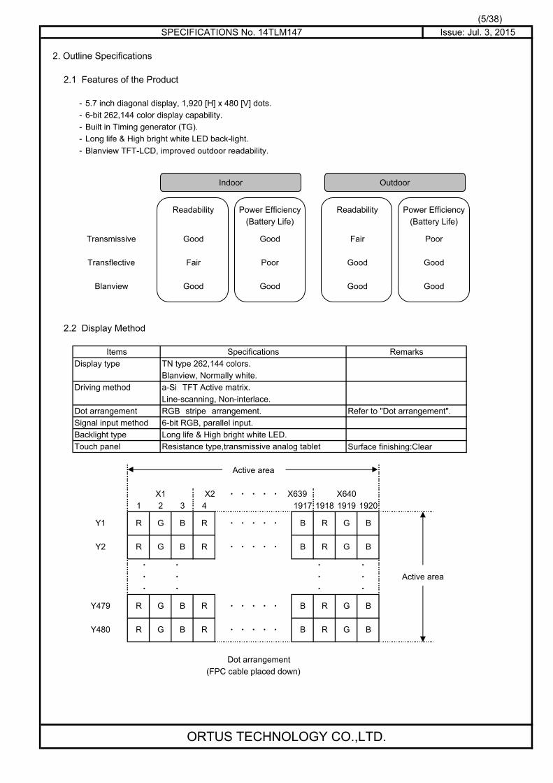
8. Description of Operation
8.1 Power On/Off Sequence
The sequence of the Power On/Off and the signal input must defend the following conditions.
- Please input the logic signal after turning on VDD.
- Please input AVDD after turning on VDD or at the same time.
- Please input V1, V5, V6, V10 and VCOM voltage after turning on AVDD.
- Please input VGL after turning on VDD.
- Please input VGH after turning on VGL.
Power Off sequence is assumed to be opposite of the above mentioned sequence.
Please refer Power On/Off recommended sequence is shown in the figure below.
V1,V5,V6,V10,VCOM voltage input
VGH
AVDD
VDD
VSS
VGL
logic signal input
8.2 Power On Clear
There is a limitation between Power On and POCB (power on clear) .
Please defend the following conditions.
90%
VDD
T
POCB
T>1ms
ORTUS TECHNOLOGY CO.,LTD.

(21/38)
SPECIFICATIONS No. 14TLM147 Issue: Jul. 3, 2015
8.3 "DISP" On/Off Sequence
It explains the Display on/off sequence.
After Display on,"White" data is outputted for 16-Frames first,from the falling edge of the following VSYNC signal.
1 2 15 16 17
DATA
output
OFF ON
After Display off,"White" data is outputted for 5-Frames first,from the falling edge of the following VSYNC signal.
Please turn off the power supply promptly after OFF of "DISP".
1 2 3 4 5
DATA
output
ON OFF
ON OFF
ORTUS TECHNOLOGY CO.,LTD.
DISP
VSYNC
INVALID White(3Fh) VALID
Backlight
DISP
VSYNC
Power
VALID White(3Fh) INVALID
Backlight

(22/38)
SPECIFICATIONS No. 14TLM147 Issue: Jul. 3, 2015
9. Circuit
9.1 Driving Circuit Example (AVDD = 12.0V)
Example of OP AMP:NJM2742M
TFT-LCM Reference Circuit
This circuit design is for reference purposes only.Appropriate component values may be different.
Please evaluate on your side.
ORTUS TECHNOLOGY CO.,LTD.
VDD
HSYNC
CLK
VSS
VSYNC
VGLVSS
VDD
VDD
VSS1
2 VGL
VDD
VGH
V5
V1
POCB
DISP
RL
UD
VSS
VDD
DE
HSYNC
VSYNC
CLK
TEST5,6
D[05:00]
TEST3,4
D[15:10]
TEST1,2
D[25:20]
VCOM
VSS
VSS
CLK
HSYNC
VSYNC
D[25:20]
D[15:10]
D[05:00]
DE
POCB
DISP
POCB
DE
DISP
3
VGH 4
8
9
POCB 10
DISP 11
VSYNC
12
HSYNC
13
CLK
14
15
16
17
18
19
20:21
22:27
28:29
30:35
36:37
38:43
44
45
D[25:20]
D[15:10]
D[05:00]
5 AVDD
V10
V6
6
7
D[05:00]
D[15:10]
D[25:20]
DE
AVDD
UD
RL
VDD
AVDDAVDD
VGHVGH
VGLVGL
RLRL
UDUD
F28kΩ
-
+OP AMP
F2kΩ
F20kΩ
4.7kΩ
F12kΩ
0.1uF25V
1uF16V
0.1
uF
25
V
1uF25V
10uF6.3V
1uF50V
10uF25V
VSS
VSS
VSS
VSS
VSS
VSS
F10kΩ
-
+OP AMP
F9kΩ
0.1
uF
25
V
F9kΩ
-
+OP AMP
F12kΩ
0.1
uF
25
V
F3kΩ
-
+OP AMP
F23kΩ
0.1
uF
25
V
AVDD
1uF16V
1uF16V
1uF16V
0.1uF25V
-
+OP AMP
1uF16V

(23/38)
SPECIFICATIONS No. 14TLM147 Issue: Jul. 3, 2015
9.2 LED Circuit
BLH1
BLL1
BLH2
BLL2
9.3 Touch Panel Circuit
XL YD XR YU
ORTUS TECHNOLOGY CO.,LTD.
YU
XL
YD
XR
Up
Down
RightLeft

(24/38)
SPECIFICATIONS No. 14TLM147 Issue: Jul. 3, 2015
10. Characteristics
10.1 Optical Characteristics < Measurement Condition >
Measuring instruments: CS1000(KONICA MINOLTA), LCD7200(OTSUKA ELECTRONICS),
EZcontrast160D(ELDIM)
Driving condition: Typical Rating of "6. Recommended Operating Conditions".
Optimized VCOMDC
Backlight: IL=10.2mA
Measured temperature: Ta=25゜C
Item Symbol Condition MIN TYP MAX Unit Remark
TON [Data]= - - 40 ms 1 ※
3Fh→00h
TOFF [Data]= - - 60 ms
00h→3Fh
CR [Data]= 360 600 - 2 3Fh/00h
- 2.3 -
Left θL [Data]= - 80 - deg 3 ※
Right θR 3Fh/00h - 80 - deg
Up φU CR≧10 - 60 - deg
Down φD - 65 - deg
x [Data]=3Fh 4y
5
[Data]=3Fh 300 450 - cd/m2 6Brightness distribution [Data]=3Fh 70 - - % 7
※ Measured in the form of LCD module.
ORTUS TECHNOLOGY CO.,LTD.
Note No.
Res
pons
etim
e
Rise time
Fall time
Vie
win
ga
ng
leC
on
tra
stra
tio
Backlight ON
Backlight OFF
Center brightness
* Note number 1 to 7: Refer to the APPENDIX of "Reference Method for Measuring Optical Characteristics".
White ChromaticityWhite chromaticity range
Burn-inNo noticeable burn-in image shall
be observed after 0.5 hours ofwindow pattern display.

(25/38)
SPECIFICATIONS No. 14TLM147 Issue: Jul. 3, 2015
【White Chromaticity Range】
Ta=25゜C0.26 0.34
0.26 0.28
0.27 0.26
0.33 0.26
0.36 0.31
0.36 0.38
0.35 0.39
0.29 0.39
White Chromaticity Range
10.2 Temperature Characteristics
< Measurement Condition >
Measuring instruments: CS1000(KONICA MINOLTA), LCD7200(OTSUKA ELECTRONICS)
Driving condition: Typical Rating of "6. Recommended Operating Conditions".
Optimized VCOMDC
Backlight: IL=10.2mA
Backlight ON
※
※
※ Measured in the form of LCD module.
ORTUS TECHNOLOGY CO.,LTD.
40 or more
x y
ItemSpecification
RemarkTa=-20゜C Ta=70゜C
TON 200 msec or less
Contrast ratio CR 40 or more
Display QualityNo noticeable display defect or ununiformityshould be observed.
Use the criteria forjudgment specified in thesection 11.
30 msec or less
Fall time TOFF 300 msec or less 50 msec or less
Response time
Rise time
0.24
0.26
0.28
0.30
0.32
0.34
0.36
0.38
0.40
0.42
0.22 0.24 0.26 0.28 0.30 0.32 0.34 0.36 0.38 0.40
x
y

(26/38)
SPECIFICATIONS No. 14TLM147 Issue: Jul. 3, 2015
11. Criteria of Judgment
11.1 Defective Display and Screen Quality
Test Condition: Observed TFT-LCD monitor from front during operation with the following conditions
Driving Signal Raster Patter (RGB, white, black)
Signal condition [Data]: 3Fh, 18h, 00h (3 steps)
Observation distance 30 cm
Illuminance 200 to 350 lx
Backlight IL=10.2mA
Uneven brightness on dot-by-dot base due to defective Refer to table 1
TFT or CF, or dust is counted as dot defect
(brighter dot, darker dot)
High bright dot: Visible through 2% ND filter at [Data]=00h
Low bright dot: Visible through 5% ND filter at [Data]=00h
Dark dot: Appear dark through white display at [Data]=18h
Invisible through 5% ND filter at [Data]=00h ignored
Uneven brightness (white stain, black stain etc) Invisible through 1% ND filter
Point-like 0.25mm< φ0.20mm< φ ≦0.25mm
φ ≦0.20mmLiner 3.0mm<length and 0.08mm<width
length≦3.0mm or width≦0.08mm
Flaw on the surface 0.05mm<W
of the Touch panel
0.03<W≦0.05mm 2<L≦5mm N≦5
L≦2mm Ignored
W≦0.03mm Ignored
Use boundary sample
for judgment when necessary
φ(mm): Average diameter = (major axis + minor axis)/2Table 1 Permissible number: N
Permissible distance between same color bright dots
(includes neighboring dots): 3 mm or morePermissible distance between same color high bright dots
(includes neighboring dots): 5 mm or more
<Landscape model>
B zone Division of A and B areas
B area: Active area
A zone Dimensional ratio between A and B areas: 1: 4: 1 (Refer to the left figure)
1 4 1
ORTUS TECHNOLOGY CO.,LTD.
Defect item Defect content Criteria
Dis
pla
y Q
ua
lity
Line defect Black, white or color line, 3 or more neighboring defective dots
Dot defect
Scr
ee
n Q
ua
lity
Dirt
Foreignparticle
Others
Flaw
AreaHighbright
dot
Lowbright
dot
Dark dot
A 0 2 2
B 2 4 4
Total 2 4 4
1
6
7
Total
3
4
Not exists
1
Criteria
N=0
N≦2
Ignored
N=0
Ignored
Conform to the criteria of point-like foreign particles.

(27/38)
SPECIFICATIONS No. 14TLM147 Issue: Jul. 3, 2015
11.2 Screen and Other AppearanceTesting conditions
Observation distance 30cm
Illuminance 1200~2000 lx
Flaw Ignore invisible defect when the backlight is on. Applicable area:
Stain Active area only
Bubble
Dust 3.2 "Outward form")
Dent
Corner area Unit:mm
a≦3
b≦3
c≦t (t: glass thickness)
a,b≦0.5 is ignored
n≦2
Others Unit:mm
a≦5
b≦1
c≦t (t:glass thickness)
a,b≦0.5 is ignored
Maximum permissible number
of chipping off on a side is 5.
Concentric interference fringe
(Test method) Size: 1/3 or less of Active area.
Darkness: comply with the boundary sample.
D≦φ0.2mm Ignored
φ0.2<D≦φ0.6mm N≦2
φ0.6mm<D N=0
(D: Average diameter of valley part)
H≦0.4mm is acceptable.
ORTUS TECHNOLOGY CO.,LTD.
Remark
Criteria
None
Po
lari
zer
(Refer to the section
Item Appearance
No functional defect occurs
FPC cable
Item Criteria
To
uch
Pa
ne
l
FisheyeFilm
surface
Puffiness
S-case
No functional defect occurs
Interferencefringe
Observe the Panel surface from 60 degrees angleto the surface under white fluorescent lamp (Triplewavelength lamp)
Glasschipping
Progressive crack
60°120°
b
a c
a
b
c
D
D
Touch Panel
0.4mm
H

(28/38)
SPECIFICATIONS No. 14TLM147 Issue: Jul. 3, 2015
12. Reliability Testnumber of failures
/number of examinations
Ta=80°C 240hr 0/3
Ta=-30°C 240hr 0/3
Ta=60°C,RH=90% 240hr 0/3
non condensing ※
Tp=70°C 240hr 0/3
Tp=-20°C 240hr 0/3
Tp=40°C,RH=90% 240hr 0/3
non condensing ※
-30←→80°C(30min/30min) 100 cycles 0/3
Confirms to EIAJ ED-4701/300 0/3
C=200pF,R=0Ω,V=±200V
Each 3 times of discharge on and power supply
and other terminals.
C=250pF, R=100Ω, V=±12kV 0/3
Each 5 times of discharge in both polarities
on the center of screen with the case grounded.
Pull the FPC with the force of 3N for 10 sec. 0/3
in the direction +/- 90-degree to its
original direction.
Pull the FPC with the force of 3N for 10 sec. 0/3
in the direction +/-180-degree to its
original direction. Reciprocate it 3 times.
Total amplitude 1.5mm, f=10~55Hz, X,Y,Z 0/3
directions for each 2 hours
Use ORTUS TECHNOLOGY original jig 0/3
(see next page)and make an impact with
peak acceleration of 1000m/s2 for 6 msec with
half sine-curve at 3 times to each X, Y, Z directions
in conformance with JIS C 60068-2-27-2011.
Acceleration of 19.6m/s2 with frequency of 0/1 Packing
10→55→10Hz, X,Y, Zdirection for each
30 minutes
Drop from 75cm high. 0/1 Packing
1 time to each 6 surfaces, 3 edges, 1 corner
Note:Ta=ambient temperature Tp=Panel temperature
※ The profile of high temperature/humidity storage and High Temperature/humidity operation
(Pure water of over 10MΩ・cm shall be used.)
ORTUS TECHNOLOGY CO.,LTD.
Test item Test conditionD
ura
bili
ty t
est
High temperature storage
Low temperature storage
High temperature & highhumidity storage
High temperature operation
Low temperature operation
High temp & humid operation
Thermal shock storage
Impact test
Pa
ckin
g t
est
Packing vibration-proof test
Packing drop test
Me
cha
nic
al e
nvi
ron
me
nta
l te
st
Electrostatic discharge test(Non operation)
Surface discharge test(Non operation)
Vibration test
FPC tension test(FPC of LCD only)
FPC bend test(FPC of LCD only)
storage:60operation:40
ordinarytemperature 90%RH
0h
0.5
h
1h
24
1h
24
1.5
h
24
2h
ordinaryhumidity
25
75%RH
60%RH
temperature
relative humidity

(29/38)
SPECIFICATIONS No. 14TLM147 Issue: Jul. 3, 2015
Table2.Reliability Criteria
Measure the parameters after leaving the monitor at the ordinary temperature for 24 hours
or more after the test completion.
item Standard Remarks
Display quality No visible abnormality shall be seen.
Contrast ratio 40 or more Backlight ON
ORTUS TECHNOLOGY Original Jig
Tension Test Method for FPC cable
Bend Test Method for FPC cable
ORTUS TECHNOLOGY CO.,LTD.
1mm
1mm
LCD Monitor
Original jig
Screw
LCDMonitor
LCD Monitor (Surface side)
-180゜+180゜
FF
FPC cable
+90°
-90°
LCD Monitor (Surface side) FPC cable
F
F
(30/38)
SPECIFICATIONS No. 14TLM147 Issue: Jul. 3, 2015
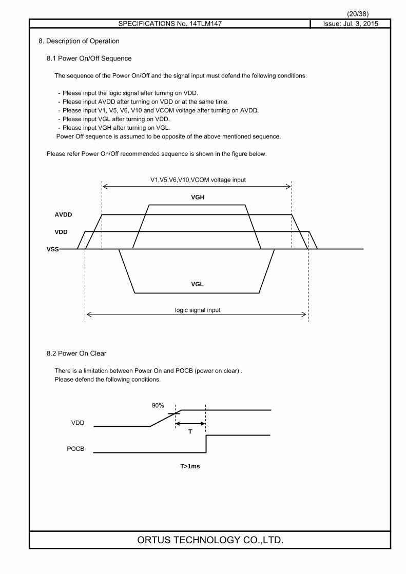
13. Packing Specifications
Remark: The return of packing materials is not required.
TRAY A-PET
SEALING BAG
INNER CARTON Corrugated cardboard
INNER BOARD Corrugated cardboard
OUTER CARTON Corrugated cardboard
Drier Moisture absorber
Packing tape
EXTRA OUTER CARTON Corrugated cardboard Quantity of products in one carton:
FOAM SHEET Anti-static polyethilene
ORTUS TECHNOLOGY CO.,LTD.
①
④
⑤
⑥
⑦
②
③
⑨
⑧
Gross weight : Approx. 7.1Kg
(198mm)
4pcsx7=28pcs
Specs., MaterialPacking item name
Dimension of extra outer carton
H : Approx.
D : Approx.
W : Approx.
(338mm)
(549mm)
Step 1.
Step 2.
Step 3.
Step 4.
Step 5.
Step 6.
Step 7.
Step 8.
Each product is to be placed in one of the cut-outs of the traywith the display surface facing upward.(4 products per tray)Each tray is to be piled up in same orientation and the trays bein a stack of 7.One empty tray is to be put on the top of stack of 7 trays.2 packs of moisture absobers are to be placed on the top trayas shown in the drawing.Put piled trays into a sealing bag.Vacuum and seal the sealing bag with the vacuum sealingmachine.The stack of trays in the plastic back is to be inserted into ainner carton.A corrugated board is to be placed on the top and on thebottom of the inner carton.The two corrugated boards and the inner carton is to beinserted into an outer carton.The outer carton needs to sealed with packing tape as shownin the drawing.The model number, quantity of products, and shipping date areto be printed on the outer carton.If necessary, shipping labels or impression markings are to beput on the outer carton.The outer carton is to be inserted into a extra outer carton withsame direction.The extra outer carton needs to sealed with packing tape asshown in the drawing.The model number, quantity of products, and shipping date areto be printed on the extra outer carton.If necessary, shipping labels or impression markings are to beput on the extra outer carton.
Packing specification(S=FREE)

(31/38)
SPECIFICATIONS No. 14TLM147 Issue: Jul. 3, 2015
14. Handling Instruction14.1 Cautions for Handling LCD panels
Caution
(1) Do not make an impact on the LCD panel glass because it may break and you may get injured from it.
(2) If the glass breaks, do not touch it with bare hands.
(Fragment of broken glass may stick you or you cut yourself on it.
(3) If you get injured, receive adequate first aid and consult a medial doctor.
(4) Do not let liquid crystal get into your mouth.
(If the LCD panel glass breaks, try not let liquid crystal get into your mouth even toxic property
of liquid crystal has not been confirmed.
(5) If liquid crystal adheres, rinse it out thoroughly.
(If liquid crystal adheres to your cloth or skin, wipe it off with rubbing alcohol or wash
it thoroughly with soap. If liquid crystal gets into eyes, rinse it with clean water
for at least 15 minutes and consult an eye doctor.
(6) If you scrap this products, follow a disposal standard of industrial waste
that is legally valid in the community, country or territory where you reside.
(7) Do not connect or disconnect this product while its application products is powered on.
(8) Do not attempt to disassemble or modify this product as it is precision component.
(9) If a part of soldering part has been exposed, and avoid contact (short-circuit) with a metallic part of the case etc. about FPC of this model, please.
Please insulate it with the insulating tape etc. if necessary.
The defective operation is caused, and there is a possibility to generation of heat and the ignition.
(10) Since excess current protection circuit is not built in this TFT module, there is the possibility that LCD module or peripheral circuit become feverish and burned in case abnormal operation is generated.
We recommend you to add excess current protection circuit to power supply.
(11) The end part of glass and film of touch panel has conductivity, and avoid contact (short-circuit)
with electroconductive case etc.. There is a possibility of setting up a defective touch panel,
and insulate it for the case suppression (cushion etc.) if necessary, please.
Caution
ORTUS TECHNOLOGY CO.,LTD.
This mark is used to indicate a precaution or aninstruction which, if not correctly observed, mayresult in bodily injury, or material damages alone.
!
!
(32/38)
SPECIFICATIONS No. 14TLM147 Issue: Jul. 3, 2015
14.2 Precautions for Handling
1) Wear finger tips at incoming inspection and for handling the TFT monitors to keep
display quality and keep the working area clean.
Do not touch the surface of the monitor as it is easily scratched.
2) Wear grounded wrist-straps and use electrostatic neutralization blowers to prevent static
charge and discharge when handling the TFT monitors as the LED in this TFT monitors
is damageable to electrostatic discharge.
Designate an appropriate operating area, and set equipment, tools, and machines properly
when handling this product.
3) Avoid strong mechanical shock including knocking, hitting or dropping to the TFT monitors
for protecting their glass parts. Do not use the TFT monitors that have been experienced
dropping or strong mechanical shock.
4) Do not use or storage the TFT monitors at high temperature and high humidity environment.
Particularly, never use or storage the TFT monitors at a location where condensation builds up.
5) Avoid using and storing TFT monitors at a location where they are exposed to direct
sunlight or ultraviolet rays to prevent the LCD panels from deterioration by ultraviolet rays.
6) Do not stain or damage the contacts of the FPC cable .
FPC cable needs to be inserted until it can reach to the end of connector slot.
During insertion, make sure to keep the cable in a horizontal position to avoid an oblique insertion.
Otherwise, it may cause poor contact or deteriorate reliability of the FPC cable.
7) Do not bend or pull the FPC cable or carry the TFT monitor by holding the FPC cable.
8) Peel off the protective film on the TFT monitors during mounting process.
Refer to the section 14.5 on how to peel off the protective film.
We are not responsible for electrostatic discharge failures or other defects
occur when peeling off the protective film.
14.3 Precautions for Operation
1) Since this TFT monitors are not equipped with light shielding for the driver IC,
do not expose the driver IC to strong lights during operation as it may cause functional failures.
2) In case of powering up or powering off this LCD module, be sure to comply the sequence as instructed in this specification.
3) Optimize VCOMDC within recommended operating conditions.* When VCOMDC is not an optimal value, flicker and image sticking will be occurred.
4) Do not plug in or out the FPC cable while power supply is switch on.
Plug the FPC cable in and out while power supply is switched off.
5) Do not operate the TFT monitors in the strong magnetic field. It may break the TFT monitors.
6) Do not display a fixed image on the screen for a long time.Use a screen-saver or other measures to avoid a fixed image displayed
on the screen for a long time. Otherwise, it may cause burn-in image
on the screen due the characteristics of liquid crystal.
ORTUS TECHNOLOGY CO.,LTD.

(33/38)
SPECIFICATIONS No. 14TLM147 Issue: Jul. 3, 2015
14.4 Storage Condition for Shipping Cartons
Storage environment
・ Temperature 0 to 40゜C
・ Humidity 60%RH or less
・ Atmosphere
・ Time period 3 months
・ Unpacking
・ Maximum piling up 7 cartons
14.5 Precautions for Peeling off the Protective film
A) Work Environment
a) Humidity: 50 to 70 %RH, Temperature15 to 27゜C
b) Operators should wear conductive shoes, conductive clothes, conductive finger tips
and grounded wrist-straps. Anti-static treatment should be implemented to work area's floor.
c) Use a room shielded against outside dust with sticky floor mat laid
at the entrance to eliminate dirt.
B) Work Method
a) Use an electrostatic neutralization blower to blow air on the TFT monitors to
its lower right when FPC cable placed down.
Optimize direction of the blowing air and the distance between the TFT monitors
and the electrostatic neutralization blower.
b) Peel off the tab slowly (spending more than 2 secs to complete)
by pulling it to opposite direction.
When FPC cable placed down. Direction of blowing air
(Optimize air direction and the distance)
ORTUS TECHNOLOGY CO.,LTD.
The following procedures should taken to prevent the driver ICs from charging and discharging.
No-condensing occurs under low temperature with high humidity condition.
No poisonous gas that can erode electronic components and/or wiringmaterials should be detected.
The followings work environment and work method are recommended to prevent the TFT monitors fromstatic damage or adhesion of dust when peeling off the protective films.
To prevent damages caused by static electricity, anti-static precautionary measures(e.g. earthing, anti-static mat) should be implemented.

(34/38)
SPECIFICATIONS No. 14TLM147 Issue: Jul. 3, 2015
APPENDIXReference Method for Measuring Optical Characteristics and Performance
1. Measurement Condition (Backlight ON)
Measuring instruments: CS1000(KONICA MINOLTA), LCD7200(OTSUKA ELECTRONICS),EZcontrast160D(ELDIM)
Driving condition: Refer to the section "Optical Characteristics"
Measured temperature: 25゜C unless specified
Measurement system:
Measurement point:
Dark box at constant temperature
TFT monitor Luminance meter
LCD7200: 220mm
CS1000: 362mm
Measurement is made after 30 minutes of lighting of the backlight.
Measurement point: At the center point of the screen
Brightness distribution: 9 points shown in the following drawing.
<Landscape model>
1
2
2
1
Dimensional ratio of active area
Backlight IL=10.2mA
ORTUS TECHNOLOGY CO.,LTD.
See the chart below. The luminance meter is placed on the normal line ofmeasurement system.
At the center of the screen unless otherwise specified
1 2 12

(35/38)
SPECIFICATIONS No. 14TLM147 Issue: Jul. 3, 2015
Measurement Condition (Contrast ratio Backlight OFF only)
Measuring instruments: LCD7200(OTSUKA ELECTRONICS),Ring Light(40,000 lx,φ58)
Driving condition: Refer to the section "Optical Characteristics"
Measured temperature: 25゜C unless specified
Measurement system: See the chart below.
Measurement point: At the center of the screen.
ORTUS TECHNOLOGY CO.,LTD.
300mm
Luminance meter
TFT monitor
80mm
Ring Light
φ5820°

(36/38)
SPECIFICATIONS No. 14TLM147 Issue: Jul. 3, 2015
2. Test MethodNotice Item Test method Measuring Remark
instrument
1 Response Measure output signal waveform by the luminance LCD7200 Black displaytime meter when raster of window pattern is changed from [Data]=00h
white to black and from black to white. White display
[Data]=3Fh
TON
White White Rise time
TOFF
White Fall time
Black
TON TOFF2 Measure maximum luminance Y1([Data]=3Fh) and CS1000 Backlight ON
minimum luminance Y2([Data]=00h) at the center of LCD7200 Backlight OFFthe screen by displaying raster or window pattern.
Then calculate the ratio between these two values.
Contrast ratio = Y1/Y2
Diameter of measuring point: 8mmφ(CS1000)
Diameter of measuring point: 3mmφ(LCD7200)3 Move the luminance meter from right to left and up EZcontrast160D
and down and determine the angles where
contrast ratio is 10.
5 White Measure chromaticity coordinates x and y of CIE1931 CS1000
chromaticity colorimetric system at [Data] = 3Fh
Color matching faction: 2°view
6 Burn-in Visually check burn-in image on the screen after 0.5 hours of "window display" ([Data]=3Fh/00h).
7 Center Measure the brightness at the center of the screen. CS1000brightness
8 Brightness (Brightness distribution) = 100 x B/A % CS1000distribution A : max. brightness of the 9 points
B : min. brightness of the 9 points
ORTUS TECHNOLOGY CO.,LTD.
Black
100%
90%
10%
Verticalφ
0%
Contrast ratio
Viewingangle
Horizontalθ

(37/38)
SPECIFICATIONS No. 14TLM147 Issue: Jul. 3, 2015
* Linearity Measurement of Touch Panel
LE(%)=∆V/(Vin-Vout)×100
LEmax(%)=∆Vmax/(Vin-Vout)×100
ORTUS TECHNOLOGY CO.,LTD.
∆V
V
B1(Vin)
B2(Vout)
d D0distance

(38/38)
SPECIFICATIONS No. 14TLM147 Issue: Jul. 3, 2015
Cautionary instruction to handle a Touch-panel
Cushion (between Touch Panel Chassis) Design
1) A cushion is required to be placed between Touch Panel and customer’s chassis and there is a designated area
to attach it. Attachment at area inside Input Prohibition Area must be forbidden.
If cushion was located inside Input Prohibition Area, Upper Electrode may be push constantly
and which may cause the electrode breakage at the position falling on the edge of adhesive;
it eventually results in Touch Panel malfunction in the future. (Please see “NG-1”)
2) Be attention to the cushion material you use. In the case that too soft cushion was used,
the cushion may protrude into Prohibition Area by being push strongly; which may result in the electrode breakage.
Eventually there is a chance that the electrode breakage leads to the malfunction of Touch Panel in the future.
(Please see “NG-2”)
3) Cushion is required to be attached at the side of Customer's chassis.
Attaching a cushion at the side of Upper Electrode Film has a chance to deform the film and
lead to the malfunction of Touch Panel in the future.
Design Guidance of Chassis (Front Part)4) Be attention to stay Input Prohibition Area away from touching and/or drawing by a stylus pens in order to
avoid the electrode breakage and potential malfunction of Touch Panel. (Please see “NG-3”)
We recommend customers to design chassis (front case) being able to protect Input Prohibition Area.
5) Clearance between customer’s chassis and Touch Panel surface is certainly required in order to avoid
erroneous input caused by a collision of the edge of chassis. (Please see “NG-4”)
A clearance of 0.3 to 0.7mm is recommended.
Design Guidance of Chassis (Side Part)
6) Upper Electrode and Lower Electrode fall on the edge of Touch Panel outline.
Redundant design having enough clearance to avoid electric short with chassis is highly recommended.
(Please see “NG-5”)
Example of Recommended Chassis Design
Refer to "3.2 Outward Form". As a terminal resistance has individual specificity, calibration to align the displaying and
the sensing position one each is mandatory before use.
ORTUS TECHNOLOGY CO.,LTD.
NG-3 NG-4 NG-5
Be
fore
Co
mp
res
sio
nA
fte
rC
om
pre
ss
ion
Cu
shio
n D
efo
rmat
ion
OK NG-1 NG-2
Attach to Chassis SideCushion
Upper Electrode Film
Adhesive
Lower Electrode Film
Customer's Chassis
To
uc
h p
an
el
Related Documents