CAD Techniques for Robust FPGA Design Under Variability by Akhilesh Kumar A thesis presented to the University of Waterloo in fulfillment of the thesis requirement for the degree of Doctor of Philosophy in Electrical and Computer Engineering Waterloo, Ontario, Canada, 2010 c Akhilesh Kumar 2010

Welcome message from author
This document is posted to help you gain knowledge. Please leave a comment to let me know what you think about it! Share it to your friends and learn new things together.
Transcript

CAD Techniques for Robust FPGADesign Under Variability
by
Akhilesh Kumar
A thesispresented to the University of Waterloo
in fulfillment of thethesis requirement for the degree of
Doctor of Philosophyin
Electrical and Computer Engineering
Waterloo, Ontario, Canada, 2010
c© Akhilesh Kumar 2010

I hereby declare that I am the sole author of this thesis. This is a true copy of the thesis,including any required final revisions, as accepted by my examiners.
I understand that my thesis may be made electronically available to the public.
ii

Abstract
The imperfections in the semiconductor fabrication process and uncertainty in operatingenvironment of VLSI circuits have emerged as critical challenges for the semiconductorindustry. These are generally termed as process and environment variations, which leadto uncertainty in performance and unreliable operation of the circuits. These problemshave been further aggravated in scaled nanometer technologies due to increased processvariations and reduced operating voltage.
Several techniques have been proposed recently for designing digital VLSI circuits un-der variability. However, most of them have targeted ASICs and custom designs. Theflexibility of reconfiguration and unknown end application in FPGAs make design undervariability different for FPGAs compared to ASICs and custom designs, and the techniquesproposed for ASICs and custom designs cannot be directly applied to FPGAs. Very fewtechniques have been proposed for FPGA design under variability, with varying degrees ofimprovement in timing/power variability. However, these have not dealt with leveragingCAD, architecture and circuits co-design methodologies for FPGA design under variability,and further, have not accounted for the impact of the variability in Vdd arising due to IRdrops which is important because the performance of a circuit becomes more sensitive toprocess parameters as Vdd is reduced.
An important design consideration is to minimize the modifications in architecture andcircuit to reduce the cost of changing the existing FPGA architecture and circuit. Thework in this thesis develops CAD and architecture/circuit design techniques for FPGAs toimprove the timing and power yield of FPGA designs under process variations. In the caseof environment variations this work focuses on developing design techniques for reducingIR-drops. The focus of this work can be divided into three principal categories, whichare, improving timing yield under process variations, improving power yield under processvariations and improving the voltage profile in the FPGA power grid.
The work on timing yield improvement implements a Statistical Static Timing Analysis(SSTA) framework to analyze the circuit delay under process variations, such that thestatistical distribution of the critical delay can be computed. In this work, the structureof the interconnect is analyzed and it is shown that an optimum number of buffers can beinserted in the interconnect to reduce the variation in circuit delay. Several interconnectarchitectures are analyzed, under the constraints of the FPGA structure, to find the bestarchitecture which leads to smallest (µ + 3σ) of the critical delay. The placement androuting tools are then enhanced such that the delay variability is accounted for whenoptimizing the critical delay of the circuit. Results indicate that up to 28% improvementin (µ+ 3σ) of the critical delay can be obtained from the proposed methodology.
The work on power yield improvement for FPGAs selects a low power dual-Vdd FPGAdesign as the baseline FPGA architecture for developing power yield enhancement tech-
iii

niques. A low power FPGA architecture is selected because, before applying power yieldenhancement techniques to a design, it is necessary that a low power design technique isimplemented. The power yield enhancement technique proposed in this work is essentiallya CAD technique for placement and dual-Vdd assignment. The proposed CAD techniquesreduce the correlation between leaking FPGA elements such that the total variability ofleakage is reduced and power yield is improved. Results indicate that an average reductionof 15% in leakage variability can be obtained from the proposed methodology, with anaverage of 7.8% power yield improvement. A mathematical programming technique is alsoproposed to determine the parameters of the buffers in the interconnect such as the sizesof the transistors and threshold voltage of the transistors, all within constraints, such thatthe leakage variability is minimized under delay constraints. Results show a reduction of26% in leakage variability without any delay penalty.
The variability in supply voltage in the power grid occurs due to currents being drawnby the underlying devices. The IR-drops in the power grid leads to reduced speed of thecircuit and may also affect the functionality of the design. To reduce IR-drops in thepower grid of FPGAs two CAD techniques are proposed in this work. The first techniqueis an IR-drop aware place and route technique which reduces the high currents drawn inlocal regions of the chip to reduce the IR-drops. The placement and routing routines areenhanced to incorporate the information about the current distribution profile in the powergrid. This is done by redistributing the blocks and nets in such a way so that the spatialdistribution of the switching activity profile is more smooth. The CAD techniques result inmaximum IR-drop reduction of up to 53% and a reduction in standard deviation of spatialsupply voltage distribution by up to 66%.
The second technique is also a CAD technique applied at the clustering stage, wherethe LUTs are clustered into fixed size logic blocks. The idea here again is to reduce thecurrents being drawn in a local region. This is achieved by carefully selecting the LUTs tobe added to form a cluster. This is because if a cluster has many LUTs with high switchingactivity nets, then that cluster will experience a large IR-drop. The clustering techniqueis enhanced such that the new IR-drop aware clustering technique takes into account theswitching activities of the nets in the current cluster and the switching activities of the netsconnected to potential LUTs that can be added to the current cluster. Results indicatethat up to 36% reduction in maximum IR-drop and 27% reduction in standard deviationof the spatial distribution of Vdd can be achieved from the proposed techniques.
iv

Acknowledgements
This thesis is dedicated to my parents. My mother, who is my first teacher, and ever fullof her untiring support and encouragement, gave me the strength of character for all mypursuits. My father taught me the importance of discipline and hard work with singleminded devotion. Amidst all the different pursuits, they taught me how to lead a life ofprinciples and righteousness. And many more things that I have imbibed and learned fromthem have shaped me as I am today.
Without the invaluable guidance, encouragement and support from my supervisor Prof.Mohab Anis, this thesis would not have been possible. It was his constant guidance thathas seen me through this work. Mohab has not only been my supervisor but also a mentorand a friend as well and I have sought his opinion and guidance on many things, whichhave always been honest, helpful and trustful. He gave me the freedom and flexibility inmy research and provided continuous guidance and support in my research pursuits. I amtruly grateful and thankful to him for all his help and support and I am glad to say thatI have really learned a lot from him during the last six and half years, first as a Master’sstudent and then as a PhD student.
The committee members have also helped a lot in bringing my thesis in the currentshape and I am thankful to all of them. Prof. Mark Aagaard, who was also my MAScthesis reader, gave very valuable comments on this thesis which have helped in improvingthis thesis tremendously. I also had an opportunity to work as a teaching assistant for Prof.Mark Aagaard and learned a lot while working with him. Prof. Manoj Sachdev’s commentshelped me gain a better insight and improve this thesis. Prof. Yehia Massoud, who wasmy external examiner, provided me with good comments on my thesis and gave someconstructive suggestions for this work. I am also thankful to Prof. Eihab Abdel-Rahmanand my co-supervisor Prof Karim Karim for reviewing my thesis.
I am thankful to Prof. Andrew Kennings who has always been very helpful and withwhom I have had many discussions on research and teaching. I am thankful to my col-leagues at the VLSI research lab with whom I have had not only technical discussions butalso shared lighter moments. Javid, Vasudha, Hassan, Ahmed and Mohamed Abu-Rahmahave all been a part of my stay at Waterloo. The administrative and technical staff at theDepartment of Electrical and Computer Engineering have always been very helpful andprompt with their support. Wendy Boles has helped me by going out of the way so manytimes that I cannot thank her enough. Phil Regier has always promptly helped me with allthe technical issues relating to either hardware or software. I would also like thank NizarAbdallah and Georges Nabaa at Actel Corp., Mountain View, California, for their supportduring my visit to the company in Fall 2008.
My stay at Waterloo as a graduate student, of almost six and half years, first as aMaster’s student and then as a PhD student has been made memorable due to so many
v

people that it is impossible to name all of them. My roommates were always there withall their support and I have shared so much with them. Aashish, Sachin and Sarvagya,with whom I have spent such a wonderful time that I cannot imagine my stay at Waterloowithout them. Sachin, always ready with his comments on anything, Sarvagya, ever eagerto carry out his pranks and Aashish, quietly observant, are some of the cherished memories.We have together celebrated many occasions and talked about so many things that theyhave become great friends and some of the closest friends for life. Niraj has been sucha close and helpful friend with whom I have shared many ups and downs and had longdiscussions on many things. Srinath has always been very helpful and a close friend withwhom I have spent a lot of wonderful time. Adi has been a great friend with whom Ihave been part of so many activities. Nikita has been very nice and has cooked wonderfuldishes on many occasions. I will also remember the fun times with Shaweta during myearlier part of stay at Waterloo. Guru, Neeraj, Jyotsna, Navneet, Prashant, Abir, Aniket,Bala and many others have also been a part of my experiences at Waterloo. My friendsfrom undergraduate days, Gunjan, Roopesh, Santosh, Amitesh and Nagendra have alwayssupported me throughout my graduate studies.
During the later part of my PhD I met Jalaj, and then Darya, Prachi and Shubham.Jalaj has been my roommate and is someone very close to me and he has always been fullof support. Darya is not only a wonderful friend but also became so close to me that sheis like a sister to me and has always encouraged me and wished the best for all my efforts.Shubham has been such a nice and close friend through all my joys and sorrows. Prachibecame a very good friend during the short time that I knew her at Waterloo. I have hada great time with them during the last year of my PhD. Thanks are due to Anupam andSurbhi and their son Anav who have treated me very warmly and friendly during all myvisits to California.
Finally, I cannot appreciate enough the great emotional support that I received frommy sisters and cousins. My sisters, Kanchan and Shashi, have always been a source ofsolace for me. My cousin, Sharad, has always supported, encouraged and helped me inmy endeavors. We have discussed so many things in such wonderful terms that talking tohim always made me happy. I also remember how my cousins Shailly, Rashmi, Pallavi,Himanshu and Sameer were full of good wishes for my work and eagerly waited for myvisits to India. Special word of appreciation is also due to my uncles Indra Mohan andShekhar from whom I have learned so many things in life, right from my childhood days,and who have always been a source of constant support. I would also like to thank all myfamily members for their constant support and encouragement in all my endeavors.
vi

Contents
List of Tables xi
List of Figures xiv
1 Introduction 1
1.1 Motivation . . . . . . . . . . . . . . . . . . . . . . . . . . . . . . . . . . . . 1
1.2 Thesis Organization . . . . . . . . . . . . . . . . . . . . . . . . . . . . . . . 2
2 FPGA Architecture and CAD Overview 4
2.1 Introduction . . . . . . . . . . . . . . . . . . . . . . . . . . . . . . . . . . . 4
2.2 FPGA Architecture . . . . . . . . . . . . . . . . . . . . . . . . . . . . . . . 4
2.2.1 Logic Block . . . . . . . . . . . . . . . . . . . . . . . . . . . . . . . 4
2.2.2 Routing Resources . . . . . . . . . . . . . . . . . . . . . . . . . . . 6
2.2.3 I/O Blocks . . . . . . . . . . . . . . . . . . . . . . . . . . . . . . . . 8
2.3 CAD Tools . . . . . . . . . . . . . . . . . . . . . . . . . . . . . . . . . . . 8
2.3.1 Synthesis . . . . . . . . . . . . . . . . . . . . . . . . . . . . . . . . 9
2.3.2 Placement . . . . . . . . . . . . . . . . . . . . . . . . . . . . . . . . 10
2.3.3 Routing . . . . . . . . . . . . . . . . . . . . . . . . . . . . . . . . . 12
2.4 VPR and T-VPack . . . . . . . . . . . . . . . . . . . . . . . . . . . . . . . 13
3 Background and Related Work 16
3.1 Introduction . . . . . . . . . . . . . . . . . . . . . . . . . . . . . . . . . . . 16
3.2 Classification of parameter variations . . . . . . . . . . . . . . . . . . . . . 16
vii

3.2.1 Process variations . . . . . . . . . . . . . . . . . . . . . . . . . . . . 17
3.2.2 Voltage Variations . . . . . . . . . . . . . . . . . . . . . . . . . . . 19
3.2.3 Temperature Variations . . . . . . . . . . . . . . . . . . . . . . . . 19
3.3 Modeling of process variations . . . . . . . . . . . . . . . . . . . . . . . . . 20
3.3.1 Principal Components Analysis (PCA) Model . . . . . . . . . . . . 20
3.3.2 Quad-Tree Model . . . . . . . . . . . . . . . . . . . . . . . . . . . . 21
3.4 Yield of a design . . . . . . . . . . . . . . . . . . . . . . . . . . . . . . . . 23
3.5 Managing Variability in ASICs . . . . . . . . . . . . . . . . . . . . . . . . . 25
3.5.1 Process Variations . . . . . . . . . . . . . . . . . . . . . . . . . . . 25
3.5.2 Supply Voltage Variations . . . . . . . . . . . . . . . . . . . . . . . 26
3.6 FPGA Design under Variations . . . . . . . . . . . . . . . . . . . . . . . . 27
3.7 Proposed Techniques . . . . . . . . . . . . . . . . . . . . . . . . . . . . . . 29
4 Design for Timing Yield 32
4.1 Introduction . . . . . . . . . . . . . . . . . . . . . . . . . . . . . . . . . . . 32
4.2 Statistical Static Timing Analysis . . . . . . . . . . . . . . . . . . . . . . . 33
4.3 Proposed Technique . . . . . . . . . . . . . . . . . . . . . . . . . . . . . . . 36
4.3.1 Impact of Segment Length on Variability . . . . . . . . . . . . . . . 36
4.3.2 Routing Architecture Evaluation . . . . . . . . . . . . . . . . . . . 40
4.3.3 Variability-Aware Placement and Routing . . . . . . . . . . . . . . 43
4.4 Evaluation, Results and Discussions . . . . . . . . . . . . . . . . . . . . . . 45
4.4.1 Experimental Details . . . . . . . . . . . . . . . . . . . . . . . . . . 45
4.4.2 Results and Discussions . . . . . . . . . . . . . . . . . . . . . . . . 45
4.5 Conclusions . . . . . . . . . . . . . . . . . . . . . . . . . . . . . . . . . . . 51
5 Design for Power Yield 53
5.1 Introduction . . . . . . . . . . . . . . . . . . . . . . . . . . . . . . . . . . . 53
5.2 Targeted FPGA Architecture . . . . . . . . . . . . . . . . . . . . . . . . . 54
5.2.1 Statistical Power Model . . . . . . . . . . . . . . . . . . . . . . . . 56
5.3 Proposed Methodology . . . . . . . . . . . . . . . . . . . . . . . . . . . . . 59
viii

5.3.1 Preliminaries . . . . . . . . . . . . . . . . . . . . . . . . . . . . . . 59
5.3.2 Placement Methodology . . . . . . . . . . . . . . . . . . . . . . . . 60
5.3.3 Dual-Vdd Assignment . . . . . . . . . . . . . . . . . . . . . . . . . 65
5.4 Evaluation, Results and Discussions . . . . . . . . . . . . . . . . . . . . . . 67
5.4.1 Experimental Details . . . . . . . . . . . . . . . . . . . . . . . . . . 67
5.4.2 Estimating leakage distribution and yield . . . . . . . . . . . . . . . 67
5.4.3 Results and Discussions . . . . . . . . . . . . . . . . . . . . . . . . 69
5.5 Conclusions . . . . . . . . . . . . . . . . . . . . . . . . . . . . . . . . . . . 73
6 Interconnect Design under Process Variations 74
6.1 Introduction . . . . . . . . . . . . . . . . . . . . . . . . . . . . . . . . . . . 74
6.2 Impact of Process Variations on Leakage and Delay . . . . . . . . . . . . . 75
6.2.1 Process Parameters and Variations . . . . . . . . . . . . . . . . . . 75
6.2.2 Leakage Modeling . . . . . . . . . . . . . . . . . . . . . . . . . . . . 76
6.2.3 Delay Modeling . . . . . . . . . . . . . . . . . . . . . . . . . . . . . 76
6.2.4 Variation Modeling . . . . . . . . . . . . . . . . . . . . . . . . . . . 77
6.3 Proposed Methodology . . . . . . . . . . . . . . . . . . . . . . . . . . . . . 79
6.3.1 Deterministic Optimization . . . . . . . . . . . . . . . . . . . . . . 80
6.3.2 FOSM Based Model: Accounting for Variability . . . . . . . . . . . 80
6.4 Evaluation, Results and Discussions . . . . . . . . . . . . . . . . . . . . . . 81
6.5 Conclusion . . . . . . . . . . . . . . . . . . . . . . . . . . . . . . . . . . . . 83
7 IR-Drop Aware Place and Route 84
7.1 Introduction . . . . . . . . . . . . . . . . . . . . . . . . . . . . . . . . . . . 84
7.2 Power Grid Model . . . . . . . . . . . . . . . . . . . . . . . . . . . . . . . 85
7.3 Proposed Methodology . . . . . . . . . . . . . . . . . . . . . . . . . . . . . 87
7.3.1 IR-Drop Aware Placement . . . . . . . . . . . . . . . . . . . . . . . 88
7.3.2 IR-Drop Aware Routing . . . . . . . . . . . . . . . . . . . . . . . . 91
7.4 Experimental Details, Results and Discussions . . . . . . . . . . . . . . . . 92
7.4.1 Experimental Details . . . . . . . . . . . . . . . . . . . . . . . . . . 92
7.4.2 Results and Discussions . . . . . . . . . . . . . . . . . . . . . . . . 93
7.5 Conclusions . . . . . . . . . . . . . . . . . . . . . . . . . . . . . . . . . . . 99
ix

8 IR-Drop Aware Clustering 100
8.1 Introduction . . . . . . . . . . . . . . . . . . . . . . . . . . . . . . . . . . . 100
8.2 Proposed CAD Flow . . . . . . . . . . . . . . . . . . . . . . . . . . . . . . 100
8.3 Proposed Clustering Technique . . . . . . . . . . . . . . . . . . . . . . . . 102
8.4 Results and Discussions . . . . . . . . . . . . . . . . . . . . . . . . . . . . 110
8.4.1 Trade-offs and Advantages . . . . . . . . . . . . . . . . . . . . . . . 112
8.5 Conclusions . . . . . . . . . . . . . . . . . . . . . . . . . . . . . . . . . . . 116
9 Conclusions and Future Work 117
9.1 Conclusions . . . . . . . . . . . . . . . . . . . . . . . . . . . . . . . . . . . 117
9.2 Future Work . . . . . . . . . . . . . . . . . . . . . . . . . . . . . . . . . . . 118
References 127
x

List of Tables
4.1 Routing architecture evaluation . . . . . . . . . . . . . . . . . . . . . . . . 41
4.2 Routing architecture evaluation: % Improvement . . . . . . . . . . . . . . 42
4.3 Benchmark sizes . . . . . . . . . . . . . . . . . . . . . . . . . . . . . . . . . 46
4.4 Results of Variability-Aware Design for Timing Yield . . . . . . . . . . . . 47
5.1 Results of variability aware placement . . . . . . . . . . . . . . . . . . . . . 70
6.1 Results of variability aware and deterministic optimizations . . . . . . . . . 82
7.1 Results of IR-Drop Aware Design . . . . . . . . . . . . . . . . . . . . . . . 93
8.1 Results of IR-Drop Aware Clustering . . . . . . . . . . . . . . . . . . . . . 111
8.2 Power savings and runtime for IR-drop aware clustering . . . . . . . . . . 115
9.1 Summary of Proposed Techniques . . . . . . . . . . . . . . . . . . . . . . . 118
xi

List of Figures
2.1 A basic FPGA . . . . . . . . . . . . . . . . . . . . . . . . . . . . . . . . . 5
2.2 Programmable switches used in SRAM-based FPGAs . . . . . . . . . . . . 5
2.3 A 2-input LUT . . . . . . . . . . . . . . . . . . . . . . . . . . . . . . . . . 5
2.4 Basic Logic Element [1] . . . . . . . . . . . . . . . . . . . . . . . . . . . . . 6
2.5 Cluster based logic block [1] . . . . . . . . . . . . . . . . . . . . . . . . . . 7
2.6 Island style routing architecture [1] . . . . . . . . . . . . . . . . . . . . . . 7
2.7 Basic CAD flow for FPGAs . . . . . . . . . . . . . . . . . . . . . . . . . . 8
2.8 Synthesis procedure for FPGAs . . . . . . . . . . . . . . . . . . . . . . . . 9
2.9 VPR CAD flow . . . . . . . . . . . . . . . . . . . . . . . . . . . . . . . . . 14
3.1 Variation in Timing and Leakage [2] . . . . . . . . . . . . . . . . . . . . . . 17
3.2 A general classification of the parameter variations . . . . . . . . . . . . . 18
3.3 Grid Model for PCA . . . . . . . . . . . . . . . . . . . . . . . . . . . . . . 21
3.4 Layer model for representing the spatially correlated process parameters . . 22
3.5 CDF of a circuit delay to determine the yield . . . . . . . . . . . . . . . . 24
3.6 PDF of a circuit delay and speed binning applied to improve the yield . . . 24
3.7 Interaction between process variations, environments variations and theirimpact on power and delay . . . . . . . . . . . . . . . . . . . . . . . . . . . 31
4.1 Merging arrival times . . . . . . . . . . . . . . . . . . . . . . . . . . . . . . 34
4.2 Impact of buffers on the delay variability . . . . . . . . . . . . . . . . . . . 38
4.3 Delay variability reduction using shorter segments . . . . . . . . . . . . . . 39
4.4 Extra wire segments in routing . . . . . . . . . . . . . . . . . . . . . . . . 39
xii

4.5 A section of routing fabric showing different segment lengths . . . . . . . . 41
4.6 The PDFs for the baseline and variability aware implementations for thebenchmark apex4 . . . . . . . . . . . . . . . . . . . . . . . . . . . . . . . 51
4.7 The CDFs for the baseline and variability aware implementations for thebenchmark apex4 . . . . . . . . . . . . . . . . . . . . . . . . . . . . . . . . 52
5.1 Dual-Vdd logic block implementation for power reduction . . . . . . . . . . 56
5.2 Example illustrating the impact of placement on leakage pdf. Spatial corre-lation causes the variance of leakage to increase. . . . . . . . . . . . . . . 61
5.3 (a) Placement is fairly spread out throughout the FPGA, which leads toreduced leakage variance. (b) Placement more concentrated, higher leakagevariance. . . . . . . . . . . . . . . . . . . . . . . . . . . . . . . . . . . . . . 63
5.4 Variability-Aware Dual-Vdd assignment technique . . . . . . . . . . . . . . 65
5.5 Power distribution without and with variability aware placement for alu4 . 71
5.6 Power distribution without and with variability aware placement for seq . . 72
5.7 CDF of power distributions for alu4 for the baseline implementation andvariability aware placement . . . . . . . . . . . . . . . . . . . . . . . . . . 72
6.1 Interconnect in FPGAs having buffered switches evenly spaced. . . . . . . 74
6.2 Schematic of a buffered switch. The SRAM cell controls the pass transistor. 75
6.3 CDFs for the deterministic and the variability-aware optimizations. . . . . 83
7.1 Mesh style power grid model . . . . . . . . . . . . . . . . . . . . . . . . . . 85
7.2 Proposed IR-drop aware Place and Route CAD flow . . . . . . . . . . . . . 87
7.3 Current distribution for baseline implementation: des . . . . . . . . . . . . 94
7.4 Voltage distribution for baseline implementation: des . . . . . . . . . . . . 94
7.5 Current distribution for IR-drop aware implementation: des . . . . . . . . 95
7.6 Voltage distribution for IR-drop aware implementation: des . . . . . . . . 95
7.7 Current distribution for baseline implementation: s38417 . . . . . . . . . . 96
7.8 Current distribution for IR-drop aware implementation: s38417 . . . . . . 96
7.9 Ratio of the circuit delay for the IR-drop aware and baseline implementation 98
8.1 Proposed IR-drop aware CAD flow . . . . . . . . . . . . . . . . . . . . . . 101
xiii

8.2 Logic cluster with input and output nets. . . . . . . . . . . . . . . . . . . . 103
8.3 Criticality tie breaking technique [3] . . . . . . . . . . . . . . . . . . . . . . 105
8.4 Computing the transition density cost during clustering. . . . . . . . . . . 106
8.5 Current and voltage distribution for the baseline implementation: alu4 . . 112
8.6 Current and voltage distribution for the IR-drop aware implementation: alu4 112
8.7 Current distributions for the baseline and IR-drop aware implementations:ex1010 . . . . . . . . . . . . . . . . . . . . . . . . . . . . . . . . . . . . . . 113
8.8 Ratio of the circuit delay for the IR-drop aware and baseline implementations.114
xiv

Chapter 1
Introduction
1.1 Motivation
Integrated circuits are now virtually present in all high-performance computing, commu-nications, and consumer electronics applications. With the increasing complexity of theseapplications, there has been a growing need to integrate the functions of these applicationsin smaller packages. To enable this integration, the semiconductor technology is continu-ously being scaled in the nanometer regime. The high level and complexity of integrationalong with scaled nanometer technologies present many enormous and critical challengeswhich must be effectively managed by the designers. In the nanometer technologies, thetwo most important design challenges cited by the semiconductor industry are the increas-ing leakage power and the process variations in device characteristics. These two seriousissues threaten the life time of silicon technology, and will hinder the development of themicroelectronics industry if not addressed. Standby leakage power has been growing at analarming rate, and constitutes a larger fraction of the total chip power in current and futuretechnology generations. Moreover, the manufacturing process of nanometer transistors andstructures has introduced several new sources of variation that have made the control ofprocess (device dimensions) variations more difficult. Additionally, environmental varia-tions are caused by uncertainty in the environmental conditions during the operation of achip, namely, power supply and temperature fluctuations. Both the process and the en-vironmental variations significantly impact the chips’ performance, power dissipation andreliability, and thereby reduce the yield of a design. In recent years several techniqueshave been proposed for addressing the standby leakage power. The leakage power problemis further aggravated by its strong dependence on process and environmental variations,leading to variation in leakage power which can be as high as 20X [2]. This makes it moredifficult for designs to meet a power budget resulting in yield loss. Technology scaling hasresulted in circuits which can operate at higher speeds, but this has also made the timing
1

optimization more complex. Traditionally, timing optimization has been done at all levels,where maximum savings in the clock cycles are obtained at the architecture level designoptimization. However, circuit level techniques try to further push this limit to increasethe operating clock frequency. The delays of the logic gates and interconnects are stronglydependent on the process and environmental parameters, which makes the clock frequencyto have significant variation due to variation in these parameters. Meeting the target clockfrequency with these variations is a challenge and results in timing yield loss.
Field Programmable Gate Arrays have emerged as a competitive alternative to Ap-plication Specific Integrated Circuits (ASICs) to implement designs and their popularityhave grown in recent years. FPGAs are preferred means to implement a design for lowto medium volume productions because of significant cost reduction and time-to-marketadvantages. Hence, FPGAs are now utilized extensively in various communication sys-tems/devices. The number of design starts based on FPGAs is continuously increasingbecause of advances in FPGA technology and newer architectures with improvement inspeed and area. Over the past decade, the management of leakage power in FPGA designshas always been overshadowed by performance improvement and dynamic power minimiza-tion techniques. However, with contemporary and future FPGAs being built in nanometertechnologies, leakage power cannot be ignored. This is aggravated by the very nature ofFPGAs, where typical block utilization is around 60% [4], such that 40% of the FPGA isdissipating standby leakage power! Only recently have FPGA designers started to tackleleakage power [5, 6, 7, 8]. The leakage power problem in FPGAs is further compoundedby the fact that FPGAs need more number of transistors per logic gate as compared tocustom VLSI designs and ASICs. In addition, process and environmental variations im-pact FPGAs in these principal areas: timing analysis, leakage power prediction, leakagetolerant design, and reliability. The focus of this research is to develop innovative architec-tures/circuit/CAD co-design for optimization of timing and leakage yield of FPGAs underprocess variations and improve the robustness of FPGAs under supply voltage variationsdue to IR-drops. This would enable FPGA designers to answer the following question:“How to utilize novel FPGA architecture, circuit and design automation techniques coop-eratively to maximize the FPGA design yield and improve robustness under power, timingand area constraints?”
1.2 Thesis Organization
This thesis is organized as follows:
Chapter 2 gives an overview of a typical SRAM-based FPGA architecture which istargeted in this work and is widely used in industry.
Chapter 3 describes the process and environment variations and its impact on VLSI
2

circuits. This section also explains the various modeling techniques for analyzing theimpacts of the variations and the modeling approach adopted in this work. This is thenfollowed by a discussion of the related work done for FPGAs.
Chapter 4 proposes a CAD and architecture co-design technique for improving thetiming yield of FPGA designs under process variations. Results are presented to show theimprovement in the timing yield.
Chapter 5 proposes a CAD methodology for improving the power yield of FPGAdesigns under process variations. The CAD methodology is explained and the results arepresented to show the power yield improvement.
Chapter 6 proposes a mathematical programming technique for determining the pa-rameters of the transistors of the buffers, such as the sizes and the threshold voltages, inthe FPGA interconnects for reducing leakage variability under delay constraints.
Chapter 7 proposes placement and routing techniques for improving the supply voltageprofile in the power grid of FPGAs. The proposed placement and routing techniques areexplained along with power grid modeling and the results for the improvement of voltageprofile in the power grid are discussed.
Chapter 8 proposes logic clustering technique to improve the supply voltage profilein the power grid of FPGAs. The novel clustering technique is discussed along with thetrade-offs and supply voltage profile improvement.
Chapter 9 concludes the work in the thesis and outlines future work.
3

Chapter 2
FPGA Architecture and CADOverview
2.1 Introduction
This chapter describes the FPGA architecture that has been adopted for this research. Thevarious elements of the FPGA is described and the CAD tools associated for implementingan application on the FPGA has been discussed. The CAD flow and each of the stages inthe CAD flow is explained along with their algorithms.
2.2 FPGA Architecture
A basic FPGA is shown in Fig. 2.1. The FPGA architecture is very regular in structure. Itis made up of two main components - logic blocks (CLBs) and routing resources. The logicblocks implement the functionality of the given circuit while the routing resources providethe connectivity for implementing the logic. The logic blocks have the flexibility to connectto the routing resources surrounding them. The logic blocks and the routing resources areconfigurable, so that they can be programmed to implement any logic. Though many typesof architectures have been experimented with, the most popular one is the SRAM basedarchitecture which is described below and has been used in this work [1].
2.2.1 Logic Block
The logic block of the SRAM based FPGA is LUT (look-up-table) based and are composedof basic logic elements (BLE). LUT is an array of SRAM cells to implement a truth table.
4

I/O Block Logic Block
Programmable Routing
Figure 2.1: A basic FPGA
SRAM
2 SRAM Cells
Pass Transistor Multiplexer
SRAM
Tri-State Buffer
Figure 2.2: Programmable switches used in SRAM-based FPGAs
2 Inputs
4 SRAM Cells Out
Figure 2.3: A 2-input LUT
5

k- input
LUT
DFF
Clock
Inputs Out
Figure 2.4: Basic Logic Element [1]
Fig. 2.3 shows a two input LUT. It has 4 SRAM cells and a multiplexer to select oneof the SRAM cells. The selection is done by the two select signals to the multiplexer,which serve as inputs to the truth-table. Each BLE consists of a k-input LUT, flip-flopand a multiplexer for selecting the output either directly from the output of LUT or theregistered output value of the LUT stored in the flip-flop. Fig. 2.4 shows the basic logicelement. Previous works have shown that the 4-input LUT is the most optimum size as faras logic density, and utilization of resources are concerned, and this has been widely used.Cluster based logic blocks were investigated in [1] and it was shown that the cluster basedlogic blocks are better in speed and area. The structure of a cluster based logic block isshown in Fig. 2.5. In the cluster based logic block, the logic block is made up of N BLEs.There are I inputs to the logic block such that each input can connect to all the BLEs.Also the output of each BLE can drive one of the inputs of each of the BLEs. The clockfeeds all the BLEs. The work in [1] showed that the logic clusters containing 4 to 10 BLEsachieve good performance. Each subblock is made up of a BLE and the correspondingLUT input multiplexers.
2.2.2 Routing Resources
The routing resources are of various types, but the one used in this work is the island-based architecture. In the island based architecture, the routing resources form a meshlike structure with the horizontal and vertical routing channels. The horizontal and verticalrouting channels are connected by switch boxes which are programmable and thus providethe flexibility in making the connections. The logic blocks are connected to the routingchannels through the connection boxes which are also programmable. Fig. 2.6 shows theisland style routing architecture [1]. The programmable switches used for implementingthe interconnections are shown in Fig. 2.2. These programmable switches have SRAM cellswhich can be programmed to either turn on or turn off the switch. Apart from the logicblocks and the routing resources, the clock distribution is assumed to have a dedicatednetwork. Most of the commercial FPGAs have a structure similar to the one describedabove or some variant of the above architecture.
6

I inputs
N outputs
BLE
#1
BLE
#N
.
.
.
.
Clock
Figure 2.5: Cluster based logic block [1]
Programmable
Routing Switch
Logic Block
Connection
Block
Programmable
Connection
Switch
Short Wire
Segment
Long Wire
Segment
Switch Block
Figure 2.6: Island style routing architecture [1]
7

Circuit Description (VHDL, blif, etc.)
Synthesize to logic blocks
Place logic blocks in FPGA
Route the connections between logic
blocks
FPGA configuration file
Figure 2.7: Basic CAD flow for FPGAs
2.2.3 I/O Blocks
The I/O blocks are also programmable so that they can be configured either as input oras output, or can be tri-stated.
2.3 CAD Tools
To implement a circuit on the current generation FPGAs, CAD tools are needed which cangenerate the configuration bits for the SRAM cells of the FPGAs. Usually the circuit de-scription is provided using Verilog, VHDL, SystemC, or other higher level descriptions. TheCAD tools for the FPGAs read this input and output a configuration file for programmingthe FPGA. Fig. 2.7 shows the basic CAD flow for implementing a digital circuit/systemon FPGAs [1]. The CAD flow has three main tasks: Synthesis, placement and routing. Inthe following sections synthesis, placement and routing for FPGAs are explained. SinceVPR and T-Vpack have been used in this work, the discussion will be kept in context ofthese CAD tools. Almost all of the commercial FPGA CAD flows perform the same basicfunctions of synthesis, placement and routing.
8

Netlist of basic gates
Technology-independent logic
optimization
Map to look-up tables (LUTs)
Pack LUTs into logic blocks
Netlist of logic blocks
Figure 2.8: Synthesis procedure for FPGAs
2.3.1 Synthesis
The synthesis of a netlist involves conversion of a circuit description, usually in hardwaredescription language (HDL), into a netlist of basic gates. This netlist of basic gates is thenconverted into a netlist of FPGA logic blocks. Fig. 2.8 shows the steps involved in thesynthesis of a circuit description into a netlist of logic blocks.
Technology independent logic optimization involves the removal of redundant logic andsimplification of the logic [9, 10]. The optimized netlist is then mapped to look-up tables,which is a process of identifying the logic gates that would go into a LUT [11]. The finalstep of the synthesis procedure is the clustering of the LUTs and flip-flops (for sequentiallogic) into logic blocks. The goal here is usually to minimize the number of logic blocksand/or minimize the delay. The work in [12] used a measure of closeness of LUTs to packthem into a cluster to form a logic block.
The work in [1] uses a timing driven logic block packing tool, called T-VPack. The tooltargets packing the BLEs into a cluster shown in Fig. 2.5. It needs the parameters such asnumber of BLEs per cluster, number of inputs per cluster, size of the LUTs, and numberof clocks per cluster. The first stage of the packing procedure simply forms the BLEs bypacking a register and a LUT together. Initially the packing procedure packs the BLEsgreedily into a cluster, followed by a hill climbing phase if the greedy phase is not able tofill the cluster completely.
To enable a timing driven packing, it is necessary to get an estimate of delays throughvarious paths of the netlist. To enable this computation three types of delays are modeled:
9

delay through a BLE, LogicDelay, delay between blocks in the same cluster, IntraClus-terConnectionDelay, and the delay between blocks in different clusters, InterClusterCon-nectionDelay. The values for these are set as 0.1, 0.1 and 1.0 for LogicDelay, IntraClus-terConnectionDelay and InterClusterConnectionDelay, respectively. The InterClusterCon-nectionDelay cannot be determined until the circuit has been implemented on the FPGA.However, these values represent the correct trend of values, and the performance of T-Vpack is not very sensitive to the exact values. The criticality of a connection is definedas
ConnectionCriticality(i) = 1− slack(i)
MaxSlack(2.1)
where MaxSlack is the largest slack amongst all the connections in the circuit. Anew cluster is created by selecting a seed BLE having the highest criticality amongst theun-clustered BLEs. After the seed BLE has been selected, an attraction function is usedto determine the next un-clustered BLE, B, to be added to the current cluster C. Theattraction function is given by:
Attraction(B) = α.Criticality(B) + (1− α)
[Nets(B) ∩Nets(C)
MaxNets
](2.2)
where the first term represents the timing part, and the second term represents the costof nets shared between the current cluster and the BLE under consideration. Any valueof α between 0.4 and 0.8 gives good results. The computation of Criticality of a BLE isexplained in [1] and also the tie-breaker mechanism used for the case when two or moreBLEs have the same criticality. Essentially, the tie-breaker mechanism selects that BLEwhich reduces the length of the largest number of critical paths.
The hill-climbing phase tries to add more BLEs to the cluster in case it is not full. Inthis phase adding a BLE to a cluster is allowed even if it leads to more inputs requiredfor the cluster than the maximum allowable. This is done because in some cases the BLEbeing added might have all its inputs from the BLEs in the current cluster and also mightdrive the inputs of some of the BLEs in the current cluster. In this case the number ofinputs required for the cluster decreases by one. However, this hill climbing phase increasesthe logic utilization only by 1 - 2% in some of the circuits.
2.3.2 Placement
The work in [1] developed the tool VPR for placement and routing. For placement theFPGA is considered as a set of legal discrete positions at which the logic blocks of the
10

synthesized netlist can be placed. For placement, the architecture descriptions needed byVPR are:
1. The number of logic block input and output pins.
2. The number of I/O pads that fit into one row or column of the FPGA.
3. The routing channel width (number of tracks in a routing channel).
The placement technique used in VPR is based on simulated annealing [13], whichimitates the annealing process used to gradually cool a molten metal to produce highquality metal objects. The simulated annealing works by first starting with an initialrandom placement by placing the logic blocks randomly on the available locations in theFPGA. The placement then proceeds by making a large number of moves to improve theplacement. This is done by selecting a logic block randomly and its new location alsorandomly. This would produce a change in the cost function, and if the cost functionimproves, the move is always accepted. However, if the cost function worsens, there isstill some probability of acceptance of the move. The probability of acceptance is givenby e−4C/T , where 4C is the change in the cost function and the goal is to decreasethe cost function. The T is the temperature parameter and controls the probability ofacceptance of the moves which worsen the placement. The temperature is initially set to ahigh value so that at the beginning of the annealing, virtually all the moves are accepted.The temperature is gradually decreased as the placement improves, such that finally theprobability of accepting a bad move is almost negligible. The flexibility of accepting badmoves allows the simulated annealing schedule to overcome the local minima in the costfunction.
The VPR sets the initial temperature in the same way as in [14]. The number of movesattempted at each temperature is done as in [15]. It is set to
MovesPerTemperature = InnerNum.(Nblocks)4/3 (2.3)
where the default value of InnerNum is 10, and Nblocks is the number of logic blocks in thenetlist. The fraction of moves accepted is kept close to 0.44 for as long as possible, as ityields better results [15]. However, VPR uses a new method of updating the temperature.The VPR computes the new temperature as Tnew = γ.Told, where the value of γ dependson the fraction of moves accepted at Told. The idea is to spend maximum time near thetemperatures at which large improvements in placement occur. The annealing procedureis not very sensitive to the exact value of γ, if it has the right form, γ is close to 1 ifthe fraction of moves accepted is close to 0.44, whereas γ is small if the fraction of movesaccepted is near 1 or 0. VPR has a timing driven placement and uses a cost function tooptimize both the timing and the delay. The complete timing driven placement algorithm
11

is explained in detail in [16]. The cost function for the timing driven placement developedin [16] is given by
4C = λ.4TimingCost
PreviousT imingCost+ (1− λ).
4WiringCost
PreviousWiringCost(2.4)
where 4TimingCost and 4WiringCost represent the change in the timing cost and thechange in the wiring cost, respectively, due to a move. The simulated annealing procedureis terminated when
T < ε.Cost
Nnets
(2.5)
where Nnets is the total number of nets in the circuit and the value of ε is set as 0.005.
2.3.3 Routing
The routing of the placed netlist, essentially, determines the switches that need to be turnedon in the routing resources of the FPGA. The routing algorithm in VPR is based on thePathfinder algorithm proposed in [17]. The Pathfinder repeatedly rips-up and re-routesevery net in the circuit until all congestion is resolved. One routing iteration involvesripping-up and re-routing every net in the circuit. The first routing iteration routes forminimum delay, even if it leads to congestion, or overuse of routing resources. To removethis overuse another routing iteration is performed. The cost of overusing a routing resourceis increased after every iteration. This improves the chance of resolving the congestion. Atthe end of each routing iteration all the nets are completely routed, although with somecongestion. Based on this routing, timing analysis can be done to compute the critical pathand also the slack of each source sink connection. The timing driven router uses an Elmoredelay model to compute the delays of all the connections. The criticality of a connectionbeteen source of net i and one of its sink j is computed as follows:
Crit(i, j) = max
([MaxCrit− slack(i, j)
Dmax
]η, 0
)(2.6)
where slack(i, j) is the slack available to the connection and Dmax is the delay of thecritical path. MaxCrit and η are the parameters which determine how the slack impactsthe congestion delay trade-off in the cost function. In VPR η is set to 1 and MaxCrit isset to 0.99.
The VPR creates a routing resource graph to describe the FPGA architecture andconnectivity information. The wire and the logic block pins of the FPGA are represented
12

as nodes in the routing resource graph, and the switches are represented as directed edgesin the graph. This routing resource graph is used to perform the routing.
The routing of a net is done by starting with a single node in the routing resourcegraph, corresponding to the source of the net. A wave expansion algorithm is invoked(k-1) times to connect the source to each of the net’s (k-1) sinks, in order of the criticalityof the sinks, the most critical sink being the first. The cost for using a node n during thisexpansion is given by:
Cost(n) = Crit(i, j).delay(n, topology) + [1− Crit(i, j)].b(n).h(n).p(n) (2.7)
where b(n), h(n) and p(n) are the base cost, historical congestion, and present conges-tion as explained in [1]. This procedure is repeated for each of the nets to get the completerouting.
2.4 VPR and T-VPack
The CAD tools used in this work are VPR, for placement and routing, and T-VPack forclustering of the BLEs [1]. VPR is invoked on the command line as follows [18]
vpr netlist.net architecture.arch placement.p routing.r [−options] (2.8)
where netlist.net is the circuit description providing the information about the connec-tivity of the logic blocks, architecture.arch is the architecture file which describes thearchitectural parameters of the FPGA. The output of the final placement is written inplacement.p, or, if the circuit is only being routed, the placement information is read fromthe file placement.p. The final routing information is written in routing.p. VPR has twobasic modes of operation. In the first mode, VPR places a circuit on the FPGA and routesit for minimum routing channel width. In the other mode, when the user specifies the rout-ing channel width, VPR attempts to route the circuit only once and if it is un-routable itsimply aborts, reporting that the circuit is un-routable. The VPR also provides graphicswhich shows the actual placement and routing of the logic blocks, along with the routingswitches.
T-VPack reads a netlist in the blif (Berkeley Logic Interchange Format) format havinglook-up tables (LUTs) and flip-flops (FFs) and packs these into logic blocks. The outputof the T-Vpack is in the .net format, which is a netlist of logic blocks. T-VPack is invokedon the command line by
t− vpack input.blif output.net [−options] (2.9)
13

Circuit
Logic Optimization (SIS), Technology Map to LUTs
(FlowMap)
.blif format of netlist of LUTs and
FFS
T-Vpack: Pack FFs and LUTs into Logic Blocks
.net format of netlist of logic blocks
VPR
Place the circuit or read an existing placement
Perform either global or combined global/
Detailed routing
Placement and routing statistics
FPGA
Architecture
Description
Existing
placement or
placement from
another CAD
tool
Figure 2.9: VPR CAD flow
14

where options are used to specify the size of the LUTs, cluster size, inputs per clusterand various optimization options.
The complete VPR CAD flow is shown in Fig. 2.9. SIS [19] is used for logic optimizationof the circuit. FlowMap [11] is used for technology-mapping to 4-LUTs and flip-flops.FlowMap produces an output in the .blif format. T-VPack packs the netlist into logicblocks and produces an output in the .net format. VPR is then used for the placementand routing of the netlist. Other logic optimizers and technology mappers, instead of SISand FlowMap can also be used in this CAD flow.
15

Chapter 3
Background and Related Work
3.1 Introduction
The parameter variations affect the performance and the reliability of a circuit, and tradi-tionally guard-banding has been used by providing an excess of safety margin for circuitdelay and power. This is done to ensure that the worst case condition in the variationsof process, voltage and temperature (PVT) are satisfied. However, with too many processcorners it becomes extremely difficult to determine the actual worst case corner, resultingin either too pessimistic or too optimistic designs. Further, designing at worst case cornerseverely limits the achievable performance-cost trade-off for the circuit.
The variability also results in an increased cost of manufacturing because the chipswith lower performance are discarded. The 2006 International Technology Roadmap forSemiconductor (ITRS) identifies the variability as one of the key difficult challenges in thescaled technologies. Fig. 3.1 shows the variation in leakage and frequency of microproces-sors in a wafer. It shows that for a 30% variation in frequency a 20X variation in leakageis observed.
3.2 Classification of parameter variations
The parameter variations can be broadly classified into process and environment variations.The process variations relate to all the physical variations caused during the manufacturingprocess and/or through aging, whereas the environment variations relate to the variationsin the operating environment of the chip. Fig. 3.2 shows a general classification of theparameter variations. Although the process parameter variations would in general affect thevoltage and temperature variations, the figure does not show that in order to simplify the
16

Figure 3.1: Variation in Timing and Leakage [2]
depiction. A detailed figure showing the interaction between process parameters variationsand environment variations and their impact on power and timing is shown later in thischapter.
3.2.1 Process variations
The process variations can be classified as die-to-die variations and within-die variations.The die-to-die variations have their origin in lot-to-lot variations, wafer-to-wafer variationsand within wafer variations. The die-to-die variations impact the parameters in such away that the values of the parameters remain the same for all the devices on a single die,but vary across different instances of the chip. Within-die variations cause the parametersto vary across a single die. The systematic variations arise from such phenomena that hasa predictable behavior. These variations arise from phenomena such as Optical ProximityEffect (OPC) and Chemical Mechanical Polishing (CMP). Therefore, theoretically thesevariations can be modeled and accounted for, by using deterministic analysis. However,since the layout is known at a later design stage and also the modeling is too complicated forthe deterministic analysis, it is advantageous to model these variations statistically. Therandom variations arise from the truly random processes and for these parameters onlystatistical behavior can be modeled. These variations thus need to be modeled throughrandom variables during the design phase. These random variations can be either inde-pendent for each device or can exhibit a spatial correlation. A further classification of theprocess variations based on their characteristics is as follows [20].
• Source: This relates to the variations arising from the sources such as polishing,
17

Die-to-die
Variations
Process
Within-die
RandomSystematic
Environment
Voltage Temperature
Figure 3.2: A general classification of the parameter variations
lithography, resist, etching, and doping. The non-uniform layout density resultsin a non-uniform dielectric thickness across the die, after the CMP process. Thedenser parts of the chip slows down the polishing resulting in the part getting morepolished than the other parts. Smaller feature sizes have made lithography variationsbecome more prominent. Also, the stepper lens heating, uneven lens focusing, andaberration lead to variations. The resist coating is non-uniform at the edges dueto surface tension and leads to thickness variations. After resist, the etching causesvariations due to uneven etching power and density. Since the number of dopantatoms have decreased with scaling, depositing these small number of dopant atomsuniformly for all the transistors is not possible and leads to variations in the dopantconcentration.
• Granularity: This classifies the variations according to the die-to-die or the within-die variations.
• Manifestation: This refers to the systematic and the random variations.
• Design impact: The variations in the manufacturing process results in the vari-ations in one or more design parameters such as the channel length, the thresholdvoltage and the device and the interconnect widths. Further, the channel length vari-ations impact the threshold voltage of the transistors, the channel length variationscaused due to factors such as wafer non-uniformity and lens focus and aberration.The width of the devices vary because of polishing or lithography issues.
18

• Aging: Most of the variations are static in nature, i.e., they do not change withthe age of the die. However, some parameters might vary with age, such as thenegative bias temperature instability (NBTI) effect in PMOS devices which causethe threshold voltage of the PMOS devices to increase with aging.
The process variations classified above typically manifest themselves as variations in thechannel length, gate oxide thickness, and threshold voltage fluctuations. These processvariations have been modeled in this work.
3.2.2 Voltage Variations
The supply voltage,VDD has been scaling with technology, but a lower limit is set due toreliability concerns. The switching activities and leakage currents in the different parts ofthe circuit lead to a current distribution in the power supply network which is not uniform.The non-uniformity of the current distributions and its variation with time leads to voltagedrops in the supply network across the chip which is both spatial and temporal and innature. The voltage drops occur due to resistance and inductance of the power supplynetwork. These voltage variations affect the performance of a circuit, and for example, a10% VDD variation can cause a 20% variation in the delay [20].
3.2.3 Temperature Variations
Elevated temperatures occur in chips during the operation of a chip. The temperatureincrease is due to the heat generation as a result of power dissipation through switchingand leakage. The temperature also gets affected by the ambient temperature of the chip.A higher ambient temperature would decrease the rate of heat flow from the chip to theoutside atmosphere, resulting in temperature rise of the chip. The temperature variationsare spatial and temporal in nature. The spatial temperature variations are caused dueto higher power dissipation in certain parts of the chip as compared to the other parts,resulting in hot spots in the areas with higher power dissipation. The temporal tempera-ture variations are caused due to different periods of activity. During the idle period thetemperature of the chip would be lower than during the period in which it is active. Thetemperature variations not only affect the performance of the chip but can also lead tothermal runaways.
19
3.3 Modeling of process variations
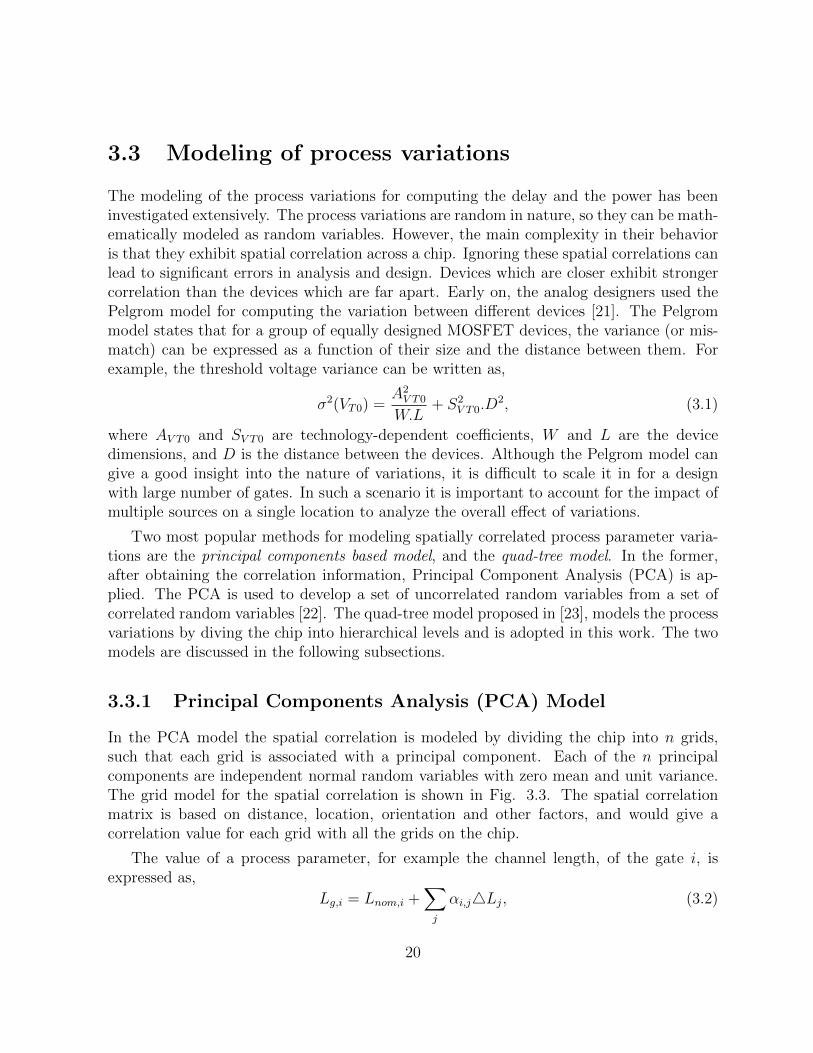
The modeling of the process variations for computing the delay and the power has beeninvestigated extensively. The process variations are random in nature, so they can be math-ematically modeled as random variables. However, the main complexity in their behavioris that they exhibit spatial correlation across a chip. Ignoring these spatial correlations canlead to significant errors in analysis and design. Devices which are closer exhibit strongercorrelation than the devices which are far apart. Early on, the analog designers used thePelgrom model for computing the variation between different devices [21]. The Pelgrommodel states that for a group of equally designed MOSFET devices, the variance (or mis-match) can be expressed as a function of their size and the distance between them. Forexample, the threshold voltage variance can be written as,
σ2(VT0) =A2V T0
W.L+ S2
V T0.D2, (3.1)
where AV T0 and SV T0 are technology-dependent coefficients, W and L are the devicedimensions, and D is the distance between the devices. Although the Pelgrom model cangive a good insight into the nature of variations, it is difficult to scale it in for a designwith large number of gates. In such a scenario it is important to account for the impact ofmultiple sources on a single location to analyze the overall effect of variations.
Two most popular methods for modeling spatially correlated process parameter varia-tions are the principal components based model, and the quad-tree model. In the former,after obtaining the correlation information, Principal Component Analysis (PCA) is ap-plied. The PCA is used to develop a set of uncorrelated random variables from a set ofcorrelated random variables [22]. The quad-tree model proposed in [23], models the processvariations by diving the chip into hierarchical levels and is adopted in this work. The twomodels are discussed in the following subsections.
3.3.1 Principal Components Analysis (PCA) Model
In the PCA model the spatial correlation is modeled by dividing the chip into n grids,such that each grid is associated with a principal component. Each of the n principalcomponents are independent normal random variables with zero mean and unit variance.The grid model for the spatial correlation is shown in Fig. 3.3. The spatial correlationmatrix is based on distance, location, orientation and other factors, and would give acorrelation value for each grid with all the grids on the chip.
The value of a process parameter, for example the channel length, of the gate i, isexpressed as,
Lg,i = Lnom,i +∑j
αi,j4Lj, (3.2)
20

(1,3)(1,2)(1,1) (1,4)
(2,1) (2,2) (2,3) (2,4)
(3,1) (3,2) (3,3) (3,4)
(4,1) (4,2) (4,3) (4,4)
Figure 3.3: Grid Model for PCA
where 4Lj is the jth component and αi,j = σi.vi,j.√λj. The σi is the standard deviation
for grid i, vij is the ith element in the jth eigenvector of the correlation matrix and λj isthe jth eigenvalue of the correlation matrix [22]. The sensitivity matrix, P, for the PCAmodel can be written as,
P =
α1,1 α1,2 α1,3 . . . α1,m
α2,1 α2,2 α2,3 . . . α2,m
α3,1 α3,2 α3,3 . . . α3,m...
......
. . ....
αn,1 αn,2 αn,3 . . . αn,m
(3.3)
where each grid of the Fig. 3.3 is associated with one column and one row. Once thespatially correlated parameters have been decomposed into a set of independent principalcomponents, any analysis can be easily performed.
3.3.2 Quad-Tree Model
In this work, the quad-tree model is selected for modeling the process parameter variations.The process parameters, such as the gate lengths of two closely placed transistors havealmost identical variation, which means that one random variable can be used for modelingthe gate lengths of both transistors. However, the gate lengths of the transistors whichare far apart need to be modeled with different random variables with spatial correlation.The quad-tree model accounts for spatial correlation through modeling the variations atseveral hierarchical levels.
A process parameter, such as channel length is represented as sum of its nominalvalue Lnom, inter-die variation 4Linter, intra-die variation 4Lintra, and random variation
21

0,0
1,00,1
1,1
0,0
1,0
2,0
3,0
0,1
1,1
2,1
3,1
0,2
1,2
2,2
3,2
0,3
1,3
2,3
3,3
Inter−Die Variation
0,0
Layer 1
Layer 2
Layer 0Intra−Die Variation
Layer 3
Random Variation
Figure 3.4: Layer model for representing the spatially correlated process parameters
4Lrandom.
Leff = Lnom +4Linter +4Lintra +4Lrandom. (3.4)
In the quad-tree model a process parameter for the complete chip is modeled at severalhierarchical levels. The entire chip is divided into several levels with each level modelinga component of the total variation. Starting from the 0th level, each level (ith level) has4i equal sized partitions as denoted in Fig. 3.4. Finally, a random level with only onegrid becomes the last level in the model. For each process parameter, there is a randomvariable associated with each of the partitions of each level. All such random variablesare independent and identically distributed. To model the process variations for a logicgate, the partition in which the logic gate lies in each of the levels is determined. Thesevariations are then added to obtain the total variation in a process parameter for a logicgate. The spatial correlation of a process parameter between two logic gates is accountedfor, by the number of common partitions they share across the different levels. Fig. 3.4illustrates the modeling of the variations for a chip with three levels. The level 0 representsthe inter-die variations because it is common for all the logic gates of the chip. Levels 1and 2 represent the intra-die variations. Consider a logic gate lying at the top right side ofthe die, i.e., at the grid location (3,0) in the level 2, and another logic gate lying adjacentto it at the grid location (2,0) in the level 2. The total channel lengths for these logic gates
22

are expressed:
Leffgate1 = Lnom + Leff0,(0,0) + Leff1,(2,0) (3.5)
+ Leff2,(3,0) + Lrandom
Leffgate2 = Lnom + Leff0,(0,0) + Leff1,(2,0) (3.6)
+ Leff2,(2,0) + Lrandom,
where Leffi,(j,k) represents the random variable for the channel length associated with thelevel i and the partition (j, k). Lrandom represents the independent random variation. Itcan be seen that the two logic gates share the [0,(0,0)] and the [1,(2,0)] partitions. Thissharing incorporates the spatial correlation in the model, implying that more the numberof grids shared, higher is the corresponding spatial correlation. Increasing the numberof levels for modeling can improve the accuracy of the model at the expense of the runtime. Since the random variables associated with the different partitions are independentwithin and across the levels, the computation of the means and the variances of the leakageor delay are easier. The total variation of a process parameter is distributed across thedifferent levels in accordance with their spatial correlation. Specifically, the total variancefor a process parameter is written as σ2 =
∑ni=0 σ
2i , where n is the total number of levels
and σi is the standard deviation of the corresponding random variable for the level i. Thequad-tree model is verified by the actual measurements in [24].
3.4 Yield of a design
The yield of a design is defined as the number of chips that meet the target performancecriterion. The performance parameter is typically the circuit delay or the power dissipation(assuming that the functionality of the circuit is correct). Under parameter variations, theperformance characteristics no longer remain deterministic, but are modeled as randomvariables. The yield of a design for a performance criterion is defined as the CDF of therandom variable representing the performance characteristic. For example, given a PDF,f(Td), of the circuit delay, Td, the yield at the target delay is calculated by computing theCDF, F (Td), and is given by the equation 3.7.
Y ield = F (Td < TargetDelay) =
∫ TargetDelay
0
f(Td)dTd (3.7)
The yield point represents the probability of a chip meeting the target delay. Fig. 3.5shows the yield point for a target delay of 8.3ns for a circuit implemented on an FPGA.In a manufacturing process fabricating a large volume of chips, 90% of the chips will meetthe target delay.
23

Delay (ns)
CDF
0
0.2
0.4
0.6
0.8
1
3 4 5 6 7 8 9 10 11
Y ield = 90%
Figure 3.5: CDF of a circuit delay to determine the yield
Delay (ns)
High Speed Bin
Medium Speed Bin
Low Speed Bin
Discard
Cut−off delay
0
0.05
0.1
0.15
0.2
0.25
0.3
0.35
0.4
0.45
3 4 5 6 7 8 9 10 11
Figure 3.6: PDF of a circuit delay and speed binning applied to improve the yield
Another technique commonly used for improving the yield of a design is binning, whichis worthwhile to point out in this discussion. An example of speed binning is shown in Fig.3.6. The figure shows the PDF of the delay of a circuit implemented on an FPGA. ThePDF is divided into three bins, the high speed bin for chips with lower circuit delays, themedium speed bin for chips with higher circuit delays, and the low speed bin for chips withhighest circuit delay. Any chip having a delay larger than the cut-off delay is discarded,leading to yield loss. The speed binning is done to improve the profitability from sellingthe chips. This is done by selling the chips in different bins at different prices, with thechips from the lowest speed bin being sold at the least price, and the chips from the higherspeed bins being sold at a higher price.
24

3.5 Managing Variability in ASICs
3.5.1 Process Variations
Traditionally, process corners have been used for analyzing designs to meet the targetedperformance, power and other design considerations at the best, nominal and worst caseprocess corners. However, this may lead to pessimistic or optimistic designs. Moreover, itis very difficult to determine whether a particular process corner is indeed a best, nominalor worst case corner, because of the significant increase in the number of varying processparameters and operating conditions with technology scaling. Therefore, to design VLSIcircuits under process variations, statistical techniques need to be adopted.
Several research works have proposed techniques for designing and analyzing VLSIcircuits and systems under process variations for timing and power optimization [25, 26,27, 28, 29, 30, 31, 32]. These papers have proposed techniques for statistical timing analysisand/or statistical power analysis and their optimization. The work in [31] proposed a designtechnique to reduce the build up of a wall of critical paths to make the circuit more robustto variations. It argues that the deterministic optimizers builds up many critical pathsto reduce the critical delay by even a small amount. Under variations these large numberof critical paths will have a higher probability to exceed the critical delay and thus causean yield loss. In [32], a dual-Vt and gate sizing algorithm was proposed which consideredthe delay and leakage variability. Results demonstrate that based on such a method,a leakage saving of 15%-35% can be obtained compared to the deterministic algorithmswhile accounting for the leakage variability. The results were reported for the 95th and 99th
percentile of the leakage power distribution. The authors in [25] proposed an AdaptiveBody Biasing technique for mitigating the impact of variability on performance and leakage.A statistically-aware clustering technique is proposed to cluster the logic gates such thata same body bias can be applied to a cluster. The results show a 38%-71% improvementin the leakage power compared to a dual-Vt implementation, and the delay variability wasreduced by 2-9X. The work in [26] targets parametric yield improvement of the design underleakage and timing constraints. The gate sizing is performed with incremental computationof the yield gradient using a heuristic proposed in the paper. A non-linear optimizer is thenused to perform the optimization. The results show that up to 40% yield improvementcan be obtained compared to a deterministically optimized circuit. In [27], the authorspropose a joint design-time and post-silicon optimization for improving the parametricyield for leakage power. This is achieved through a robust linear programming to obtainan optimal body-bias policy, once the uncertain variables are known. An improvement of5%-35% in leakage power is obtained from this methodology. The authors in [28] proposea statistical gate sizing method based on the sensitivity computation. A new objectivefunction is proposed for optimizing the circuit and an algorithm is developed for computing
25

the sensitivity. A pruning and statistical slack based approach is used, which shows animprovement of 16% in the 99-percentile circuit delay and a 31% improvement in thestandard deviation for the same circuit area. A new approach is proposed in [30] for speedbinning where instead of optimizing for yield, total profit maximization is done. This isbased on the fact that chips in different bins are sold at different prices. Again, a sensitivitybased gate sizing algorithm is proposed. An algorithm is proposed to determine the optimalbin boundaries. A joint sizing and optimal bin boundaries determination approach is alsoinvestigated. Results show that a 36% improvement in profit can be obtained from theproposed approach. In [29], a gate level method is proposed to estimate the parametricyield of a design under leakage and timing constraints by finding a joint PDF of leakage andtiming. This is necessary because the leakage and timing are correlated and the assumptionof their independence will lead to errors in joint yield computation.
However, these papers have proposed techniques for custom VLSI designs and ASICs,and cannot be directly applied to FPGAs because of the intrinsic nature of programmabilityof FPGAs. Another challenge in FPGAs is that the circuits which are finally mapped tothe FPGAs are not known and the resources for FPGAs are fixed once they are fabricated,thus limiting the flexibility for design optimization.
3.5.2 Supply Voltage Variations
Technology scaling has led to scaled wires and increased packing density of logic gates.Scaling of wires increase their resistance proportionately, and high packing density of logicgates cause more current to be drawn in a local area, which result in increased IR-dropsin the power supply network of a chip. Additionally, the currents are usually distributednon-uniformly in the chip leading to spatial non-uniformity in IR-drops. The IR-dropscause the logic gates to operate at a voltage lower than the full Vdd, which affects not onlythe switching speed of the gates, but can also affect the correct operation of logic andclock skew [33, 34]. Thus, it is very critical to develop efficient design techniques for robustpower grids which minimize IR-drops in the power network.
Several techniques have been proposed for designing a reliable power grid for a chip.Most of these techniques relate to sizing the wires of the power grid [35, 36], topologyoptimization [37, 38], and decoupling capacitances [39, 40]. Another technique proposedin [41] involves determining the pitches and sizes of the wires in a non-uniform power grid.
The techniques proposed in these papers are for custom VLSI design and/or ASICs andcannot be directly applied to FPGAs because of the programmable nature of the FPGAsand the end application to be implemented on the FPGA is unknown. This necessitatesdeveloping CAD techniques which reduce IR-drops while mapping the application to theFPGA.
26

3.6 FPGA Design under Variations
The major design challenges for FPGAs have been area and power in earlier technologies.However, in scaled nanometer technologies it is critical for the FPGA industry to addressthe design challenges stemming from the process and environment variations. Very fewpublished work exists targeting the design of FPGAs under variations [42, 43, 44, 45, 46,47, 48, 49].
The work in [49] includes process variations by creating a variation map for each FPGAchip, and then a detailed placement is performed for optimizing the timing. The variationmap describes the detailed variations in the devices and interconnects, after the fabrica-tion of the chip. The variation map is obtained by applying test circuits for each chipbefore mapping an application to the FPGA. A variation aware placement is developed forconsidering the variation in the critical delay of a circuit. This is performed in a determin-istic manner because the variation map for a chip gives the actual values of the processparameters on a chip. The reported results indicate a performance improvement, by usingthe proposed chip-wise variation aware placement, of 5.3%. However, the authors do notprovide details for obtaining the variation map, and generating a variation map for eachchip is expensive.
In [43], a placement algorithm is described for improving the timing yield of the FPGAs.The delay of a circuit is modeled as a first order canonical form of the process variations.The guard banding and speed binning is discussed and the reduction of yield due to within-die variation and correlation is explained (with speed binning). The authors propose astatistical placement methodology to reduce the yield loss. Versatile Place and Route(VPR) [1] was augmented with the statistical placement methodology, which performsSSTA at each placement iteration, and therefore, attempts to optimize the statistical delayinstead of the deterministic delay of the FPGA. Using this methodology, the authors reporta reduction in the yield loss of 5X with the guard banding and 25X with the speed binning.The authors used a 10% global and 10% local random variation in the channel length andthe threshold voltage. However, it is not related how their methodology performs in thepresence of within-die variations with spatial correlations which becomes important inscaled technologies.
Again, a variation aware placement technique is suggested for leakage power and timingin [48]. A Block Discarding Policy scheme is provided to optimize the placement underprocess variations for timing and leakage. The policy works on the principle of selecting ablock on the FPGA for the placement based on leakage and delay values. Then a leakageand a delay thresholds are chosen for such a selection methodology. Although, a thresholdvoltage variation is considered, the spatial correlations are not accounted for. The work isbased on the assumption that for an FPGA chip, the exact leakage and delay values for allthe blocks are available (i.e., with variations), and therefore, these leakage and delay values
27

can be used for optimizing the placement. Also, the VPR is modified such that each of theblocks in the VPR placement routine has the leakage and delay values with variations. Aleakage cost function is used in the placement cost function, but its mathematical form isnot provided in the paper. The results show a 14% saving in leakage by using the scheme,and a 10% improvement in the clock frequency. This improvement in clock frequency isobserved by simply providing the delays with the variations in the VPR framework. Thereis no statistical analysis of the delay and leakage, and this work depends on obtainingaccurate values of the delay and leakage for each block and each FPGA chip, which iscomputationally very expensive.
In [45], statistical leakage and timing models for computing the leakage and timingyield for FPGAs are developed. The leakage model under variations is empirically derived,whereas the timing variability model is obtained from SPICE simulations for the basiccircuit elements of the FPGA. Delay points are sampled from SPICE simulations and thedelay PDF is directly constructed from the PDF of channel length. Although leakage varieswith channel length, gate oxide thickness and threshold voltage, the delay is modeled tovary only with the channel length of the devices. For computing the leakage yield, a baselinearchitecture is assumed with the target leakage set as the nominal leakage with an offsetof 30%. The authors evaluate various combinations of logic block cluster sizes and LUTsizes in the FPGAs for their yield and the simulations indicate that some combinations canresult in an improved yield. However, the authors do not consider the spatial correlation ofthe intra-die variations of the process parameters. It is analyzed how the yield can changeif the supply voltage and the threshold voltage of the devices are changed in the FPGA.Additionally, the timing yield is analyzed for different combinations of the cluster and theLUT sizes. No CAD technique is proposed to enhance the timing and leakage yield inFPGAs.
The researchers in [44] introduce an adaptive body biasing technique for the FPGAs tocompensate for the process variations. Each FPGA chip is proposed to have a characterizerto measure the variations in the threshold voltage for each block by measuring the delaythrough the block. The body biasing can be accomplished according to the thresholdvoltage fluctuation for the block. Each tile has the extra configuration bits (2-3 SRAMbits) for determining the applied biasing, and a circuitry to apply the bias. The resultsindicate a 30.3% decrease in the standard deviation of delay for three levels of body biasing,and 3.3X reduction in the standard deviation of delay for seven levels of body biasing canbe achieved. The standard deviation of the leakage is reduced by 78% for three levels ofbody biasing, and by 18.8X for seven levels of body biasing. However, the area overheadfor each tile is 1.6%, whereas the area overhead of the characterizer is nine FPGA tiles.Further, there will be an additional cost due to the triple well process for designing theFPGAs.
The work in [47] uses the FPGA and ASIC CAD flows for a set of benchmarks to show
28

the impact of process variations on the FPGA and the ASIC implementations, for the samecircuits. One of the conclusions is that, although the impact of the process variations ismore pronounced in the case of the ASICs, its impact on the FPGAs cannot be ignored.It also proposes a variation aware routing methodology to improve the timing yield of theFPGAs, with a 3.95% improvement in the delay for the same yield, from a deterministicrouter with a 3σ guard banding for the delays of circuit elements. However, no architectureevaluations were done for routing resources, which is an important design criterion, giventhat the routing delay dominates the total delay of the circuit. Further, no statisticalplacement optimization was considered which is also a critical factor governing the overallcircuit delay and thus the timing yield.
In [42], the authors propose statistical techniques for the major steps in the FPGA CADflow, i.e., logic clustering, placement, and routing. The stochastic clustering technique pro-posed takes into account the uncertainty in the routing interconnect at the clustering level,where no information about the routing is available. The uncertainty value in the inter-connect delay arising due to the uncertainty in the interconnect usage is modeled as arandom variable apart from the process parameters. The actual values of these variablesare determined heuristically. The statistical information is embedded in the clusteringphase through the clustering cost function, by incorporating the statistical criticality ofa basic logic element. Similarly, during the placement and the routing phases the statis-tical criticality as defined in [42], is computed for the cost functions. Again, no routingarchitecture evaluations are done in this work.
No known work exists for dealing with supply voltage variations in the power grid ofFPGAs, apart from the work proposed in this thesis and discussed in chapters 7 and 8.
3.7 Proposed Techniques
These challenges in designing FPGAs under process variations in nanometer technologies,motivate the following, which are the contributions of this work.
• Timing and power yield improvement: Earlier works for FPGAs have not ac-counted for the intra-die variation with spatial correlations while performing theoptimization. The work in this thesis is based on a model suitable for both intra andinter-die process variations, thus making it more flexible. The process parametersunder consideration in this work are the channel length, substrate dopants, gate ox-ide thickness. However, the model developed is generic to incorporate any numberof process parameter variations. The timing yield improvement technique proposedin this work develops architecture enhancements along with CAD tool improvements
29

to increase the timing yield of the design. The power yield enhancement design tech-nique is essentially a CAD technique used for a low power FPGA. The power yieldimprovement targets reduction in leakage variability leading to improvement in totalpower yield.
• CAD for IR-drop reduction in FPGA power grid: This work proposes anenhanced IR-drop aware place and route technique to improve the voltage profile ofthe power grid in FPGAs by reducing IR-drops and spatial variance of the supplyvoltage. A faster technique at an earlier stage in design flow, at the clustering stageis also proposed. The IR-drop aware clustering also improves the voltage profile ofthe power grid in FPGAs in a similar way. The trade-offs associated with both thesetechniques are also analyzed.
Fig. 3.7 shows the interaction between the process variations and environment vari-ations and their impact on power and delay. This work targets power and timing yieldoptimization under process variations and improving the supply voltage profile. It does notintend to analyze and optimize impact of supply voltage variations on delay and power,and temperature variations. The figure shows various links indicating how different factorsaffect each other and also power and delay. It also shows the links that this work explores.
One of the objectives of this work was to minimize the changes to the existing architec-tures and circuits such that most of the modifications are done to CAD tools for FPGAs.This will prevent changes to the FPGA architectures and circuits which can be costly. Aswill be observed in the later chapters which describe the work, the changes to circuits andarchitectures are minimal and most of the modifications are proposed for the CAD toolsfor FPGAs. Additionally, the proposed changes to the circuits and the architecture doesnot alter the fundamental fabric of the generic SRAM-based FPGA.
30

Power YieldTiming
Leakage
Variability
Temperature
Variations
Delay Process
Supply Voltage
Variations
Yield
VariationsVariability
Timing Yield
Timing Yield
Work Done
Power
Yield
Power Yield
Figure 3.7: Interaction between process variations, environments variations and their im-pact on power and delay
31

Chapter 4
Design for Timing Yield
4.1 Introduction
This chapter explains the work on timing yield improvement for FPGAs. The timing yieldof a VLSI design is defined as the fraction of chips which meets circuit delay target, outof all the fabricated chips. This means that only those chips which meet the target circuitdelay can run at the desired frequency of operation. The rest of the chips which cannotrun at the target frequency of operation are then discarded and results in yield loss. Themain ideas and results proposed and discussed in this chapter are as follows:
1. Routing architecture enhancements for timing yield with SSTA: Earlierworks on FPGAs have not accounted for the intra-die variations with spatial corre-lations, while the optimization is performed. This work is based on a model suitablefor both the intra and the inter-die process variations, thus introducing flexibility.The process parameters under consideration in this work are the channel length, thesubstrate dopants, and the gate oxide. An analysis of the routing architectures andan evaluation of these routing architectures for their suitability under process varia-tions is performed. It is imperative that the routing architecture design is considered,because a principal part of the total delay is due to the routing segments.
2. Variability aware CAD for improved timing yield: The placement and routingtools are enhanced to enable a statistical optimization. A variability-aware placeand route technique is proposed which accounts for the timing variability throughstatistical delay information available during the place and route phases.
This chapter first discusses the statistical static timing analysis (SSTA) techniqueadopted in this work and then explains the proposed design techniques from improvingthe timing yield of FPGAs by reducing delay variability [50].
32

4.2 Statistical Static Timing Analysis
Recently, many published works have proposed techniques for the SSTA, such as [23, 51, 22,52]. The main ideas behind any SSTA technique are, (1) modeling the process parametervariations along with their correlations, and (2) computing the statistical critical delay,which can be either the block-based approach or the path-based approach. The workin [53] is a high level model for 3-D circuits which first starts with the assumption ofknowing the number of critical paths in the circuit and is based on the work in [54] for 2-Dcircuits. Also, it does not consider the spatial correlation of process parameters which leadsto additional complexity. The SSTA technique adopted in this work takes into accountthe spatial correlations of the process parameters and propagates the delays without anyassumption of knowing the critical paths.
In this work the SSTA technique proposed in [23] is adopted for computing the criticaldelay of the circuit. The inter-die and intra-die process parameter variations are modeledas discussed in the Section 3.3. The two main steps performed by the STA (and SSTA)are the propagation and the merging of the arrival times at the different circuit nodes.In the propagation step the input arrival time at a logic gate is propagated to its outputby adding the delay of the gate, whereas in the merging step the maximum of all thearrival times at the output of the gate is computed. However, in the case of the SSTA, thearrival times are random variables and the Cumulative Distribution Function (CDF) or theProbability Density Function (PDF) of the arrival times are propagated. The complexity ofthe SSTA arises from the correlation between the arrival times at the same logic gate or atdifferent logic gates. This correlation is due to two factors: the re-convergent fanouts andthe spatial correlation of the process parameters. It has been shown in [55] that ignoringthe correlation due to the re-convergent fanouts, leads to an upper bound in the statisticaldelay analysis, and as a result is conservative. However, the spatial correlation due to theprocess parameters cannot be ignored [23].
The arrival time is modeled as follows:
a = Anom +∑i
si.pi + Arandom (4.1)
where Anom is the arrival time at the nominal process parameter values, si is the sensitivityof the arrival time to the process parameter, pi, modeled as a random variable, and Arandomis the random independent component of the arrival time.
Similar to the arrival time, the delay of a gate is modeled as follows:
d = Dnom +∑i
sdi.pi +Drandom, (4.2)
where sdi is the sensitivity of the gate delay to the process parameter, pi. The arrivaltime propagation is achieved by adding the individual components of the arrival time
33

a1
a2 a3 = max(a1, a2)
Path Delay = a3 + dg
Figure 4.1: Merging arrival times
and the gate delay to obtain a canonical form of the arrival time at the gate output. Thisoperation is an exact one and does not lead to any inaccuracy. The next step is to computethe maximum of the arrival times at the gate output.
Consider two arrival times a1 = Anom,1 +∑
i si,1.pi + Arandom,1, and a2 = Anom,2 +∑i si,2.pi + Arandom,2 as shown in Fig. 4.1. The max(a1, a2) is given by the arrival time
a3 = Anom,3+∑
i si,3.pi+Arandom,3 such that each of the components of the max is calculatedas follows:
Anom,3 = max(Anom,1, Anom,2) (4.3)
si,3 = max(si,1, si,2) (4.4)
Arandom,3 = max(Arandom,1, Arandom,2) (4.5)
This process of computing the maximum of the two arrival times is not an exact compu-tation, but gives an upper bound, resulting in a conservative estimate. In case of computingthe maximum of more than two arrival times, the simple procedure outlined in (4.3) - (4.5),can result in a large error accumulation. The authors in [23] have introduced a heuristic toreduce the error. Instead of propagating one arrival time at the output of a logic gate, mul-tiple arrival times are propagated. The larger the number of the arrival times propagated,the better the accuracy is. When no merging operation is performed at any intermediatenode, the arrival time computed at the primary output is exact, but the computation com-plexity is large. At each node, the heuristic propagates only K arrival times by mergingsome of the arrival times. For all the arrival times, ai, incident on a node the maximumarrival times, mi,j, for each pair ai, aj, is calculated. All the maximum arrival times, mi,j,are arranged in descending order and the mi,j with the minimum mean replaces the ai, ajpair in the arrival time set. Thus, the number of arrival times is reduced by one. Thisprocess is repeated, until only K arrival times remain. This procedure attempts to mergeonly those arrival times which are likely to have the least or no impact on the critical delayof the circuit. The arrival times are propagated in this manner, until the primary outputor a sink is reached, where the maximum operation is again performed to obtain the upper
34

bound on the critical delay of the circuit. Some other works have instead proposed ana-lytical techniques for computing the max operation [56]. However, the proposed techniquehas the flexibility of being as accurate as desired by increasing the number of arrival timesto be propagated.
Besides the other parameters, the delay of a logic element is also dependent on thethreshold voltage of the transistors of a logic element. The threshold voltage varies withthe channel length of the transistors due to the short channel effects. In particular, a roll-off in the threshold voltage is observed as the channel length is reduced. In this work, thethreshold voltage model from BSIM4 is chosen [57]. The threshold voltage of a transistoris modeled as
V th = V th0 + V thbody − V thSCE − V thDIBL (4.6)
+ V thhalo − V thDITS,
where V thbody, is the body effect, V thSCE is the short channel effect, V thDIBL is the draininduced barrier lowering effect, V thhalo is the threshold voltage shift due to the halo pocketimplants at the drain and source junctions, and V thDITS is the drain induced thresholdshift due to the source and the drain pocket implants. The various components of thethreshold voltage are functions of the channel length, the gate oxide thickness and thesubstrate doping. The BSIM4 analytical models are employed for the threshold voltagedependence on these process parameters.
The variation in the threshold voltage due to the random dopant fluctuations is modeledas follows [58]:
σV thrdf =Q.Toxεox
√Nch.Wdm
3.L.W, (4.7)
where Wdm is the channel depletion width, Nch is the channel doping concentration, andL, W are the channel length and width, respectively. To a first order approximation smallvariations in L will not impact the random dopant fluctuations and hence variations inL and threshold voltage variations due to random dopant fluctuations can be consideredindependent. For a function y = g(x), where x is a random variable with variance σ2
x, thevariance of y is approximated by computing [59]
σ2y =
(dg(x)
dx
)2
· σ2x. (4.8)
The delay of a circuit element is expressed as a function, f(Leff ), and the variance in thedelay, σ2
delayLeff, is computed by (4.8). Similarly, the variance in the delay due to gate
oxide thickness variation σ2delayTox
is calculated. A closed form expression for f(Leff ) and
35

f(Tox) is unwieldy, and can be represented through a set equations presented in [57],and is omitted here for brevity. Since the channel length variations, the random dopantfluctuations and the gate oxide thickness variations are independent, the total variance ofdelay is calculated by:
σ2delay = σ2
delayrdf+ σ2
delayLeff+ σ2
delayTox. (4.9)
To compute the variance and the mean of the delay, it is modeled as a function ofLeff , Tox and V th. Using the statistical model, the mean and the variance of delay Dfor a logic element at location (j, k) for ith level, are computed as follows:
E{D} = D(Lnom, V thnom, T oxnom) (4.10)
+1
2
n∑i=0
(∂2D
∂Leff 2 .σ2Leff i,(j,k)
+∂2D
∂V th2.σ2V th(rdf)i,(j,k)
+n∑i=0
∂2D
∂Tox2.σ2Toxi,(j,k)
),
σ2D =
n∑i=0
(( ∂D
∂Leff
)2.σ2
Leff i,(j,k)(4.11)
+( ∂D∂V th
)2.σ2V th(rdf)i,(j,k)
+( ∂D
∂Tox
)2.σ2Toxi,(j,k)
),
where all the partial derivatives, which represent the sensitivities of the delay to the processparameters, are computed at the nominal values of these process parameters, at ith leveland location (j, k). Since the random variables, Leffi ,(j ,k), for the different values of i, j, kare independent, the delay variances are added to obtain the total delay variance.
4.3 Proposed Technique
4.3.1 Impact of Segment Length on Variability
This section proposes a theoretical basis for routing architecture enhancements in thiswork. Here a single wire segment is considered with buffers and expressions for its delay
36

and its variability are discussed. Consider a wire segment with m buffers which are equallyplaced along the length L of the wire. The propagation delay through the wire is givenby (4.12), [60]. The standard deviation of the propagation delay, under variations in thechannel length of the transistors, and the assumption that the variations are independentacross the buffers is computed from 4.12, and is given by (4.13),
tp = m
(0.69
Rd
s
(sγCd +
cL
m+ sCd
)(4.12)
+ 0.69
(rL
m
)(sCd) + 0.38rc
(L
m
)2),
σtp =0.69
s
(cL√m
+√m(sγCd + sCd)
)∂Rd
∂Leff
σLeff, (4.13)
where Rd is the resistance of the buffer (minimum-size), Cd is the input capacitance of thebuffer (minimum-size), γ is the ratio between the intrinsic output and input capacitancesof the buffers, s is the size of the buffer, r is the resistance of the wire per unit length,and c is the capacitance of the wire per unit length. In FPGAs, the wiring capacitancesdominate the total capacitance in the routing segments. This is because the routing inan FPGA requires more wiring resources than its ASIC counterpart. Also in the scaledtechnologies, interconnects have become the dominant source of delays. Consequently,(4.13) is simplified by ignoring the buffer capacitances such that
σtp =0.69
s
(cL√m
)∂Rd
∂Leff
σLeff, (4.14)
which shows that the standard deviation of the propagation delay varies inversely with√m. This implies that as the number of buffers increases for a given length of wire,
the standard deviation of the delay decreases. However, this decrease cannot continueindefinitely, because the capacitances of the buffers will start to play a more dominantrole, as the number of buffers is increased, and the terms ignored in (4.14) can no longerbe ignored.
Consider two different examples of interconnect buffers in a routing segment in anFPGA. In Fig. 4.2(a), the routing segment consists of three identical buffers, distributedthroughout the length of the wire such that the capacitance of each of the wire segmentis C1. The capacitance due to the buffers is ignored because it is much less than that ofthe wire capacitance. In the Fig. 4.2(b), the complete wire is driven by a single buffer ofthe same size, as the one in Fig. 4.2(a). The total capacitance of the wire is C2 where
37

R1
R1R1 R1
C1 C1 C1
(a)
(b)
C2 = 3C1
Figure 4.2: Impact of buffers on the delay variability
C2 = 3.C1. The average on-resistance of the buffers is given by R1 and the resistance ofthe wires is ignored because it is small compared with the on-resistance of the buffers.
With these assumptions, the simple first order expressions for the variance of delay forthe two cases are calculated, with the variation in the channel length Leff . It is assumed herethat the process variations of each of the buffers are independent. Here, it is worthwhileto point out that factors such as cross-talk can further complicate the scenario. However,cross-talk would lead to increased dominance of wire capacitance and hence the abovediscussion becomes even more relevant and important.
σ2D1
= 3.
(∂R1
∂Leff
.C1σLeff
)2
(4.15)
σ2D2
=
(∂R1
∂Leff
.3C1.σLeff
)2
(4.16)
= 3.σ2D1
The equations (4.15) and (4.16) compute the variances of the delays for the two casesin Fig. 4.2(a) and 4.2(b) respectively. It is evident that the delay variance (standarddeviation) in Fig. 4.2(b) is three (
√3) times greater than the delay variance in Fig. 4.2(a).
These expressions indicate that the number of buffers for a wire segment can be increasedto reduce the delay variance, until the buffer capacitance becomes a significant part of thetotal capacitance. Furthermore, the approximations in (4.15) and (4.16) are valid only to acertain extent and are presented to intuitively analyze the impact of the number of buffersin the routing segments.
Fig. 4.3 shows the routing of a net and how the delay variability is affected by thenumber of buffers in the routing of the nets for two different cases. Fig. 4.3 (a) illustratesa case when the routing uses fewer buffers resulting in larger delay variability, whereas inFig. 4.3 (b), more buffers are used by the net resulting in lesser delay variability.
38

µ1
3σ1
µ2
3σ2
PDFPDF
(a) Longer Segments (b) Shorter Segments
Delay Delay
µ1 + 3σ1 > µ2 + 3σ2
Figure 4.3: Delay variability reduction using shorter segments
Sink
Source
Source
(a)
(b)
Driven
Sink Extra Wire
Figure 4.4: Extra wire segments in routing
39

Another case which typically occurs in FPGAs is that of the unused parts of the tracksbeing driven by the buffers. This occurs because of the location of source and sink pairs.Consider the example illustrated in Fig. 4.4, which shows the interconnect between a pairof source and sink. In Fig. 4.4 (a), the second buffer which ultimately connects to the sinkhas to drive a long wire as well even though that is not required in the routing, and thisresults in larger delay variability in accordance to (4.14), compared to Fig. 4.4 (b), wherethe third buffer, which ultimately connects to the sink, drives a smaller wire segment notnecessary for the routing between the source and sink pair.
The above discussion shows that shorter wire segments are good for delay variability,when the wire capacitances dominate the total interconnect capacitance. However, theactual scenario in an FPGA is more complicated due to spatial correlation in the processparameters across different buffers and also the capacitance of the buffers would affect theactual mean and standard deviation of the circuit delay. Further, in case many buffers areinserted in a routing, the capacitances of the buffers will become important and thereforea simple architecture having only shorter wire segments will not suffice. An architecturewhich supports both longer and shorter wire segments is required and is explored in thiswork.
In ASICs, where there is more flexibility for buffer insertion and sizing a mathematicaloptimization problem can be devised with more accurate delay models to determine thelocation of these buffers. However, in an FPGA, since it is pre-fabricated, and the FPGAdesign cannot be targeted for a particular application, the design approach that is adoptedin this work allows routing segments which have more buffers for a given wire lengththan other routing segments. The router during the routing phase then selects the mostappropriate routing segments.
The timing yield of a design is defined as the number of chips meeting the target timingcutoff. Therefore, one of the optimization approaches can be chosen to reduce the delayvariability such that most of the chips meet the required timing. A similar approach isto reduce the delay at a certain confidence level, which can be the 3σ point on the delaydistribution curve. Since the target delay cutoff is not known for the FPGAs, the objectiveof this work is to reduce the (µ+ 3σ) delay of the circuit.
4.3.2 Routing Architecture Evaluation
A typical FPGA routing architecture is composed of horizontal and vertical routing seg-ments, connected by switch boxes. The routing fabric of an FPGA contains differentlengths of wire segments as shown in Fig. 4.5. Here, there are three different routingsegments, the wire that spans eight logic blocks with eight switch boxes, the wire thatspans eight logic blocks with four switch boxes, and the wire that spans four logic blocks
40

Length 8wire with
8 switch boxes
Length 8 wirewith 4 switchboxes
Length 4wire with
4 switch boxes
CLB
Switch Box
Figure 4.5: A section of routing fabric showing different segment lengths
Table 4.1: Routing architecture evaluation
Architecture Length 2 segment Length 4 segment Length 8 segmentarch1 10% 45% 45%arch2 20% 40% 40%arch3 30% 35% 35%arch4 40% 30% 30%arch5 50% 25% 25%
with four switch boxes. In the first case of the wire spanning eight logic blocks with eightswitch boxes, the segment has the flexibility of connecting to the vertical routing segmentsat all the intersections of horizontal and vertical routing tracks. In the second case of thewire spanning eight logic blocks with four switch boxes, the segment has the flexibility ofconnecting to the vertical routing segments at only four intersections of the horizontal andthe vertical routing segments.
An FPGA routing architecture consists of different ratios of these routing segments.For instance, in an FPGA where the routing channels have 100 tracks, the distribution canbe 20 tracks with segments of length 2, 40 tracks with segments of length 4 and 40 trackswith segments of length 8.
There can possibly be a very large number of combinations of segment lengths, resultingin as many number of routing architectures. Theoretically, all of these can be evaluated,however, the search space is too large such that it is computationally infeasible to evaluateall the possible combinations. Instead, this work intends to demonstrate that by providingsome shorter segments in the existing routing fabric the timing variability can be reduced.To this end, this work explores five different combinations of routing segments as shownin Table 4.1. The baseline architecture consists of the architecture with 50% segments oflength 4 and 50% segments of length 8. Architectures with segments of length 4 and 8 areexplored in [1], in a similar manner, but not for variability aware design.
This work proposes a theoretical basis and a methodology for exploring routing archi-tectures to reduce timing variability in FPGAs. An FPGA designer can incorporate shorter
41

Table 4.2: Routing architecture evaluation: % Improvement
Architectures → arch1 arch2 arch3 arch4 arch5Mean 3.61% 7.5% 8.79% 7.2% 5.97%Std. Dev. 9.8% 9.1% 9.3% 8.7% 8.4%
segments in the FPGA according to the design constraints and evaluate which combinationleads to best results. Indeed, the different segment length combinations explored in thiswork is not exhaustive and thus there is no guarantee that this set of combinations of rout-ing segments contains the best routing architecture for reducing timing variability. Themethodology allows an FPGA designer to to judiciously select and design routing fabricfor FPGAs, such that the timing yield can be enhanced.
Table 4.2 shows the average improvements in the (µ + 3σ) point for different archi-tectures compared to the baseline architecture for the 20 MCNC benchmarks. It can beobserved that the mean improvement for all the architectures vary between 4% and 9%.This indicates that providing smaller routing segments would invariably lead to improve-ment in timing variability. An architecture which leads to high improvements in certainbenchmarks while less improvements or degradations in other benchmarks is not desir-able. In such a case just measuring the mean improvement will lead to an inappropriatearchitecture selection. To prevent this, the standard deviations of the improvements arealso calculated to analyze the architectures. The last row in Table 4.2 lists the standarddeviation of the improvements. From the table, it can be seen that the architectures arch2,arch3, and arch4, have mean improvements better than the other benchmarks, between7% and 9%, and therefore these architectures are selected for further evaluation. To furthernarrow down the choice to one architecture, the standard deviations are also evaluated.It can be seen that although arch3 has the greatest mean improvement, arch4 is the bestcandidate because of good mean improvement and smallest standard deviation. There-fore, arch4 is selected as the candidate architecture for further evaluation. While there isno guarantee that the suggested routing architecture is the best routing architecture, theproposed methodology provides a framework and a theoretical basis to guide the design ofFPGAs for timing variability. Also, the best combination of routing segments, from amongthose evaluated, suggested in this work may not be the best for all FPGAs, depending onits application area and the benchmarks on which the FPGA is evaluated before its designis finalized. Further, an FPGA designer might have to deal to additional constraints whichmight make some routing segment combinations infeasible. However, even in such casesthe same methodology, with additional constraints, can be employed to arrive at the finalarchitecture. More discussion on the results is presented in Section 4.4.
42

4.3.3 Variability-Aware Placement and Routing
The CAD approach employed to enhance the performance of the placement and routingtool under the process variations, involves incorporating the delay variability information inthe placement and routing phase of the design flow. The VPR implements a timing drivenplacement for a netlist to map an application to an FPGA [16]. VPR uses a simulatedannealing algorithm for the placement of the logic blocks on the CLBs. It is an algorithmwhich mimics the annealing procedure to cool molten metal slowly for producing highquality metal structures. The algorithm begins with a random placement, and repeatedlymoves the logic blocks to newer locations and evaluates whether the move can be acceptedor not. The acceptance or rejection depends on the placement cost, computed by theVPR. If the move results in a reduction of the placement cost, the move is accepted. If theplacement cost increases as a result of the move, there is still some probability that themove will be accepted. The acceptance of some bad moves prevents the placement toolfrom being stuck at some local minimum.
The placement cost of the VPR is the sum of the timing cost and the wiring cost. Thetiming cost is computed on a source sink basis. For a source sink pair (i, j) [16],
Timing Cost(i, j) = Delay(i, j).Crit(i, j)crit exp, (4.17)
Crit(i, j) = 1− Slack(i, j)
Dmax
, (4.18)
where Delay(i, j) is the delay between source (i) and sink (j), Crit(i, j) is the criticalityof the connection between them, Slack(i, j) is the slack available with the source and thesink pair, Dmax is the critical path delay, and crit exp is for assigning large weights tocritical timing connections. The total timing cost is then computed as
Timing Cost =∑(i,j)
Timing Cost(i, j). (4.19)
The wiring cost is estimated by computing the bounding box of the placed logic blocks [16].Essentially, the bounding box is the smallest rectangle within which all the logic blocks liefor the current placement. The wiring cost is an estimate of the wire length used by thenetlist. The authors in [16] develop an auto-normalizing cost function for the placement.The cost function, 4C, used for the placement routine, is defined as
4C = λ.4Timing Cost
Previous T iming Cost(4.20)
+ (1− λ).4Wiring Cost
Previous Wiring Cost,
where λ is a factor for giving different weights to the timing cost and the wiring cost,4Timing Cost is the change in the Timing Cost because of the current move, and
43

4Wiring Cost is the change in the Wiring Cost because of the current move. The timingdriven placement in the VPR optimizes both the wiring cost and the timing cost dependingon the value of λ. In [16], it is proposed that λ = 0.5 and crit exp = 8 are the best valuesfor the timing and wiring cost trade-off.
Since the optimization goal under process variations is to minimize the (µ+ 3σ) pointof the critical delay, the Timing Cost evaluations is performed at the (µ + 3σ) point asshown in (4.21),
Timing Cost(i, j) = (µ+ α.σ)(i,j).Crit(i, j)crit exp, (4.21)
where α is the factor for choosing the point on the delay PDF to be optimized. In thiswork, α = 3, since the goal is to optimize the (µ + 3σ) point of the delay PDF. This isa straightforward approach resulting in a direct optimization of the (µ + 3σ) point. Thevalue of α can be conveniently chosen to optimize the targeted point.
The routing in the FPGA is based upon the Pathfinder algorithm [1]. The Pathnderrepeatedly rips-up and re-routes each net in the circuit, until all the congestion is resolved.One routing iteration involves ripping-up and re-routing each net in the circuit. The firstrouting iteration routes for the minimum delay, even if the iteration leads to congestion,or the routing resources are overused. To remove this overuse another routing iteration isperformed. The cost of overusing a routing resource increases for each iteration, therebyimproving the chance of resolving the congestion. At the end of each routing iteration allthe nets are routed, but with some congestion. Based on this routing, a timing analysis iscarried out to compute the critical path and also the slack of each source sink connection.A net is routed by starting with a single node in the routing resource graph, correspondingto the source of the net. A wave expansion algorithm is invoked k times to connect thesource to each of the net’s k sinks, in the order of the criticality of the sinks, the mostcritical sink being the first. The cost for using node n during this expansion for connectingthe sink j of the net i is expressed as
cost(n) = crit(i, j).delay(n, topology) (4.22)
+ [1− crit(i, j)].b(n).h(n).p(n),
where crit(i, j) is the criticality of the connection, delay(n, topology) is the delay of theconnection after including node n in the path, and b(n), h(n), p(n) are the base cost, thehistorical congestion, and the present congestion [1]. To incorporate the variability infor-mation in the router, the routing cost function is modified and instead of the nominal valueof delay(n, topology), its mean and standard deviation are computed as follows:
delay(n, topology) = µdelay(n, topology) (4.23)
+ 3σdelay(n, topology)
44

In the variability-aware router the 3σdelay(n, topology) is computed at each routingiteration and used in the SSTA driven routing optimization engine.
4.4 Evaluation, Results and Discussions
4.4.1 Experimental Details
The 45nm Berkeley Predictive Model is chosen as the technology node for the simulations.It is demonstrated in [24] that three levels in the quad-tree model for the process variationslead to sufficiently accurate results for SSTA, and hence five levels are chosen in this work.Since the FPGAs have a regular structure, in which a tile is replicated across the chip,instead of using 4i grids at level i, a scheme in which the grid size at level 0 is the size of theFPGA, the level 1 has the grid size of 8x8 FPGA tiles, the level 2 has the grid size of 4x4FPGA tiles, and the level 2 has the grid size of 2x2 FPGA tiles, is selected. This essentiallymeans that for any level, all the tiles within the grid has perfect correlation, for example,at level 2 all the 4 FPGA tiles in a grid will have a single random variable to represent thevariations in a process parameter. Such a scheme, as opposed to the one in which each levelis divided into 4i grids, avoids the FPGA tiles from being partitioned into more than onegrid. The last level represents the random independent variations. In case of availabilityof the fabrication data and the spatial correlation information for process parameters, thegrid sizes and the number of levels can be accurately determined by using the methodologydescribed in [24]. In the absence of actual measurement data for process variations, thechannel length variations and the gate oxide thickness variations are modeled at levels1, 2, and 3 which represent intra-die variations and models the spatial correlation in theprocess parameters between the different parts of the chip. A 3σ variation of 20% in Leffand a 3σ variation of 15% in Tox are assumed, and distributed equally over the levels[23], in the absence of the actual fabrication data for the spatial correlation. The variationin the threshold voltage, due to random dopant fluctuations is modeled at the last level,representing an independent random variable. A set of MCNC benchmarks is selected inthis work for obtaining the results.
4.4.2 Results and Discussions
To evaluate the routing architecture, several different routing architectures are simulated.The evaluation of different routing architectures are listed in Table 4.1. The idea behindexploring the routing architectures is to determine the proportion of the different routingsegments required to reduce the (µ+ 3σ) point of the critical delay.
45

Table 4.3: Benchmark sizes
Benchmarks # of CLBs Benchmarks # of CLBsalu4 192 ex5p 139apex2 240 frisc 446apex4 165 misex3 178bigkey 214 pdc 582clma 1054 s298 243des 200 s38417 802diffeq 189 s38584.1 806dsip 172 seq 221elliptic 454 spla 469ex1010 599 tseng 133
The baseline architecture is the architecture with 50% wire which spans four logic blocksand 50% wire segments spanning eight logic blocks, which was explored in [1]. This baselinearchitecture is used to measure the improvement in the (µ + 3σ) of the critical delay byusing the proposed design technique. The five routing architectures evaluated have differentpercentages of the routing segments of lengths two, four and eight. The proportion of thetrack segments spanning two logic blocks is increased and the remaining tracks are equallydivided between the segments spanning eight and four logic blocks respectively. The sizesof different benchmarks are shown in Table 4.3 in terms of number of CLBs, where eachCLB has a size of 8 BLEs.
The routing architecture does not have the flexibility to be altered once the FPGA isfabricated. Therefore, this evaluation should be performed by an FPGA designer beforethe architectural parameters of the FPGA are fixed and the FPGA is fabricated. Basedon the simulation results, as discussed in Section 4.3.2, the best architecture determinedfor reducing the variability, under the given technology and constraints, is the arch4. Theresults shown in Table 4.4 use arch4 for the variability-aware design.
Table 4.4 offers a comparison of the (µ + 3σ) delays of the baseline and the variabil-ity aware designs. Column 5 lists the improvements due to architecture enhancementsand column 6 lists the improvements after CAD optimization is applied to the FPGAwith enhanced architecture. It can be seen that with just the architecture enhancements,improvement in (µ + 3σ) delay can be obtained. Further, it can be observed that the(µ + 3σ) delay of the variability aware design improves by up to 28%, depending on thebenchmark, when variability-aware CAD optimization is applied to the enhanced FPGAarchitecture. These improvements result from reduction in the mean and the variance of thedelays. Another observation that can be made from the table is that in some benchmarksvariability-aware place and route does not lead to any improvement or slightly degrades
46

Table 4.4: Results of Variability-Aware Design for Timing Yield
Bench-marks
Baseline(µ +3σ)
Variability-Aware Architecture Improvement (µ+ 3σ) Std. Dev. Improvement YieldImprove-ment
Determin-istic CAD(µ + 3σ)(ns)
Variability-AwareCAD(µ +3σ)(ns)
Arch.Enhance-ment
Arch.and Vari-abilityAwareCAD
Arch.En-hance-ment
Arch.andVariability-AwareCAD
alu4 8.77971 8.64609 8.32891 1.52% 5.13% 16.87% 21.75% 3.00%apex2 10.2202 9.27657 9.03988 9.23% 11.54% 17.88% 18.61% 16.25%apex4 8.48323 8.49214 8.02503 -0.1% 5.40% 15.71% 18.43% 3.91%bigkey 5.73215 5.74827 6.19854 -0.3% -8.13% 7.19% 7.02% -0.44%clma 19.4209 21.3906 21.1896 -10.1% -9.1% 11.7% 15.98% -2.17%des 11.2742 9.97441 14.3802 11.5% -27.5% 13.65% 0.7% 16.12%diffeq 7.86171 5.94118 5.65697 24.4% 28.04% 18.41% 26.4% 68.23%dsip 6.11283 5.52062 5.43229 9.7% 11.13% 4.7% 5.25% 13.58%elliptic 11.5893 10.2334 10.0177 11.7% 13.56% 13.91% 18.88% 17.78%ex1010 15.2968 14.989 14.5394 2% 4.95% 15.88% 18.63% 2.94%ex5p 9.46913 8.47661 8.00807 10.5% 15.42% 15.19% 18.96% 39.91%frisc 14.4183 12.1726 12.3823 15.6% 14.12% 9.94% 16.83% 37.61%misex3 8.51963 8.00565 8.0134 6% 5.94% 18.00% 21.65% 4.59%pdc 14.4815 14.4253 14.1629 0.4% 2.2% 15.90% 17.30% 0.33%s298 12.9248 10.7352 10.8236 16.9% 16.25% 13.18% 18.62% 58.01%s38417 12.7315 13.22 11.8097 -3.8% 7.24% 13.88% 18.64% 2.95%s38584.1 9.71621 9.38845 9.09571 3.37 6.38% 10.71% 15.18% 2.87%seq 9.94624 8.61802 9.23896 13.3% 7.11% 18.83% 17.16% 24.50%spla 13.1557 13.0828 12.9597 0.6% 1.48% 14.14% 20.06% -0.224%tseng 6.57158 5.1804 5.42482 21.1% 17.45% 8.29% 10.80% 56.65%
47

the (µ+3σ) delay, for example, in the cases of frisc and misex3. This is attributed to thefact that the exact circuit delay and its variance is known only after the routing is completeand during the placement stage only an estimation can be made with regards to the delayand its variance. Further, the variance estimation is complicated by the spatial correlationfactor, and the topology of a path. So, even if two nets have same number of buffers andwire lengths, the arrival time delay variance can be significantly different depending on thespatial correlation of process parameters and their topology. However, it should be notedthat the delay variability CAD optimization approach is applicable during the mapping ofa benchmark to the FPGA, and it can be turned on only if it results in delay variabilityimprovement.
Columns 7 and 8 show the improvements in the standard deviations from architectureenhancement and architecture enhancement with variability-aware CAD, respectively. Itcan be observed that reduction in standard deviation of up to 22% can be achieved using theproposed technique. The optimization approach (architecture and variability-aware CAD)targets the reduction of the (µ+ 3σ) delay and this may result in an increase in the meanof the delay delay in the optimized design, however, the (µ + 3σ) decreases, for example,as in the case of the benchmark alu4 where the mean of the delay increases slightly in theoptimized design, but the standard deviation of the delay decreases by 21.75% leading toan overall improvement in (µ+ 3σ) delay of 5.13%.
In the cases of the benchmarks bigkey and clma the standard deviation of the criticaldelay decreases when the architecture is enhanced, but the mean delay increases such thatthe (µ + 3σ) delay increases. In the case of the benchmark clma the standard deviationof the delay decreases by 16%, but the mean delay increases by 19.5%, resulting in overalldegradation in the (µ+3σ) delay of 9.1%. In the case of benchmark des, it can be observedthat the architecture improvement leads to an improvement of 11.5% in the (µ+3σ) criticaldelay, however, when variability-aware place and route is used for this benchmark, it leadsto degradation in the (µ + 3σ) critical delay. Such differences occur across benchmarksbecause of the differences in topology of the benchmarks.
Fig. 4.6 shows the PDF of the delay distributions of the baseline and the variabilityaware design for the benchmark apex4. It can be seen that the mean and the standard de-viation of the critical delay reduces in the variability-aware design implementation leadingto reduction in (µ+ 3σ) critical delay by 5.4%. As another example, in case of the bench-mark ex1010, the mean value of the critical delay remains same in both the baseline andthe variability optimized designs, however in the case of the variability optimized designthe variance of the critical delay reduces by 18.8%, resulting in an overall improvement inthe (µ+ 3σ) delay of 4.95%.
For a given design, process variations lead to variations in the timing of the fabricateddesigns. There can be two approaches to look at the timing variability in fabricated chips.The first approach is evaluating the (µ + nσ) critical delay point of the design, where, in
48

this work n is 3. This would ensure that 99.9% of the fabricated designs would meet the(µ+ 3σ) critical delay. For example, in the case of apex2 benchmark, from Table 4.4, withvariability-aware architecture and CAD, 99.9% of the apex2 designs on the FPGA willmeet the critical delay target of 9.04ns, whereas in the case of the baseline architecturethe critical delay target needs to be relaxed to 10.22ns, such that 99.9% of the apex2designs on the FPGA can meet the critical delay requirement. This implies that withthe variability-aware architecture and CAD, the apex2 design can be operated at a higherfrequency.
The second approach works in the case when the design has to meet a specified targetdelay. The timing variability implies that not all chips will be able to meet the target delay.For example, in the case of the apex2 design, if the target delay is 8.53ns, only 87.4% ofthe designs on the baseline FPGA will meet the target delay of 8.53ns. However, in thecase of the FPGA with variability-aware architecture and CAD, 98.9% of the designs willmeet the target delay of 8.53ns. The yield of a design depends on the minimum frequencyrequirement and the maximum allowed leakage [61]. The upper cut-off limit for the criticaldelay depends on the minimum frequency requirement, whereas the lower delay cut-offdepends on the maximum allowed leakage. The timing yield of a given design for a targetcritical delay is then found by calculating the CDF of the critical delay distribution asfollows:
Y ieldTargetDelay =
∫ TargetDelay
LowerCutoffDelay
f(D)dD, (4.24)
where f(D) is the PDF of the design’s critical delay, Lower Cutoff Delay is the lowercutoff delay, which is due to the constraint on leakage, and Target Delay is the criticaldelay which must be met by the design. The target delay is intended for the minimumfrequency requirement, whereas the lower cut-off delay is intended for the maximum allowedleakage. The lower cut-off selected in this work is (µ− 2σ) delay, which discards about 2%of the chips in which variability can cause excessive leakage, thus rendering them unusable.Though this work targets timing yield, such a lower cut-off limit is required and the (µ−2σ)delay is selected for illustrative purposes, and any other value can be chosen depending onthe maximum allowed leakage for the design.
The last column in Table 4.4 shows the best case yield improvement over the baselineimplementation due to either from the architecture improvement or architecture improve-ment with variability-aware place and route. For calculating the yield improvement, thetarget and cutoff delays for the variability-aware design is selected as (µ+2σ) and (µ−2σ)respectively, corresponding to the 95% confidence level, i.e., 95% of the chips for a designwill have their critical delay between these values. To compute the corresponding yieldfor the baseline design the Target Delay is selected as the (µ + 2σ)V ariability Aware of thevariability-aware design, whereas the Lower Cutoff Delay is selected as the (µ−2σ)baselineof the baseline design. The above selection of Target Delay and Lower Cutoff Delay
49

are intended for computing the yield and any such delay values can be chosen based onthe design constraints to estimate the yield of a design.
Fig. 4.7 shows the CDF of the critical delay for the benchmark apex4 from which theyield for a given delay can be computed. For the benchmark apex4 with the variability-aware implementation, a 95.5% yield is obtained if the target delay is 7.4 ns and the lowercut-off delay is 5.13 ns. For the same target delay, and the lower cutoff delay of 4.93 nsthe baseline design implementation has a 91.5% yield. In cases of the benchmarks bigkey,clma, and spla, it can be seen that there is an yield loss. This occurs again because,although the standard deviation of the critical delay decreases in all the cases, but themean value of the delay increases, such that there is an yield loss at the target delay.For instance in case of spla, the standard deviation of the critical delay reduces by 20%,however, the mean value of the critical delay increases by 5.8%. Again, this behavior isdue to differences in topology of the benchmarks. This shows that just one architecturemight not be suitable for all the applications. A possible solution to this can be providinga few flavors of different FPGA architectures, similar to what is provided by a commercialvendor. Though this work provides results for only one architecture, an FPGA designermight choose to provide more than one FPGAs such that all the validation benchmarksare satisfied. An an example, in the case of the benchmark spla, which has a small (µ+3σ)delay improvement of 1.48% with an yield loss of 0.22% for the architecture arch4 withvaribility-aware CAD, the architecutre arch3 with the variability-aware CAD leads to animprovement of 6% in (µ+ 3σ) delay, with an yield improvement of 3.8%.
Designing a routing architecture with shorter segment lengths requires more transis-tors. The area trade-off for the proposed architecture is such that the architecture requires10% more transistors than the baseline implementation. The average dynamic power con-sumption (computed at mean frequency), for alu4, for the variability-aware implementationincreases by 1% compared to the baseline implementation.
The optimization approach proposed in this work is a two step process, in which thefirst step is to determine the routing architecture and the second step is to optimize usingvariability-aware placement. The routing architecture improvement leads to most of theimprovements in the (µ+ 3σ) critical delay, with the variability-aware place and route op-timization leading to further improvements. The run-times of the variability-aware CADoptimization and deterministic CAD optimization differ because of the statistical oper-ations performed during the optimization steps. The runtimes of the benchmarks withvariability-aware CAD vary between 20 minutes and 492 minutes for different benchmarks.The runtimes for deterministic place and route vary between 0.5 minutes and 7 minutes.For example, in the case of alu4, the deterministic place and route takes 1 minute of run-time, whereas the variability-aware place and route takes 31 minutes of run time. Theruntime of the variability-aware CAD tool, depends on the number of levels chosen inthe grid-model for SSTA, the number of grids on each level and the number of random
50

0
0.1
0.2
0.3
0.4
0.5
0.6
0.7
2 3 4 5 6 7 8 9 10
Variability
Aware
Baseline
σ2σ2 < σ1
µ2 < µ1
Delay (ns)
σ1
Figure 4.6: The PDFs for the baseline and variability aware implementations for thebenchmark apex4
variables modeled. The higher these number, greater is the accuracy at the expense ofruntime. In the case of the benchmark alu4 if only channel length variations, which is thedominant variation, is considered, the runtime for the variability-aware CAD reduces from31 minutes to 15 minutes, however, the standard deviation of the delay is underestimatedby 5.9% . For the same benchmark, if variability-aware routing is turned off, the runtimeof the CAD tool with just the variability-aware placement is 12 minutes. However, thiscomes at the expense of lesser improvement of 4.7% in (µ + 3σ) delay. If the number oflevels in the grid model for SSTA is reduced by one and only channel length variation ismodeled, the runtime of the variability-aware CAD reduces from 31 minutes to 9 minutes,with the standard deviation of the delay being underestimated by 9%. It should however,be noted that with architecture enhancements, even a deterministic place and route wouldlead to improvement in the timing variability as listed in column 5 of Table 4.4, with theruntime same as that of the deterministic place and route.
The technique proposed here for architecture and CAD enhancements is applicableto most of the industrial FPGAs, such as Virtex series from Xilinx or the Stratix fromAltera. The technique is applicable because it follows the principle of incorporating shortersegments in the routing fabric, with more buffers, which can be easily applied to manyFPGA architectures. The CAD enhancements are flexible and can be incorporated in anyCAD tool by using statistical delay models.
4.5 Conclusions
This chapter presents a variability aware design technique to reduce the impact of processvariations on the timing yield of FPGAs. The technique is twofold involving the co-design
51

BaselineYield
VariabilityAware Yield
0
0.2
0.4
0.6
0.8
1
2 3 4 5 6 7 8 9 10
Variability
Aware
Delay (ns)
Baseline
CDF
DelayLower Cutoff Target
Delay
Figure 4.7: The CDFs for the baseline and variability aware implementations for thebenchmark apex4
of the routing architecture and the variability-aware CAD optimizations. The routingarchitecture evaluations indicate that an architecture which has a certain proportion ofshorter routing segments can provide a better trade-off for the timing variability. TheCAD tool for placement and routing is enhanced to incorporate the timing variabilityto improve the timing yield of FPGAs. The results of the joint architecture and CADoptimizations indicate that the (µ+ 3σ) delay improvement of up to 28% can be achieveddepending upon the benchmark.
52

Chapter 5
Design for Power Yield
5.1 Introduction
This chapter discusses the design techniques for improving power yield in nanometer FP-GAs. The techniques proposed in this chapter are CAD techniques. Every applicationhas a power budget because of constraints due to battery life, thermal issues, etc., whichshould not be exceeded. All chips exceeding the power budget are discarded which leadsto yield loss. The chips which have total power consumption less than the power budgetcontribute to the power yield of the design. For example, in mobile and low power biomed-ical applications, an appropriate power budget is pivotal to a long battery life. For suchapplications process variations can diminish the power yield of FPGAs resulting in signif-icant financial loss. Several design techniques have been proposed for managing leakagepower in FPGAs [5], [7], [62], [63]. However, none of these techniques have included theimpact of process variations. Traditionally, process corners have been used for analyzingdesigns to meet the targeted performance, power and other design considerations at thebest, nominal and worst case process corners. However, this may lead to pessimistic oroptimistic designs. Moreover, it is very difficult to determine whether a particular processcorner is indeed a best, nominal or worst case corner, because of the significant increasein the number of varying process parameters and operating conditions with technologyscaling. Therefore, to design VLSI circuits under process variations, statistical techniquesneed to be adopted. Yield improvements directly translate to profit and even small yieldimprovements are desirable because of economic considerations [30]. These challenges indesigning low power FPGAs in nanometer technologies, and simultaneously accounting forprocess variations, motivate the following, which are contributions of this work [64]. Thecontributions of this work are as follows:
• Variability aware placement methodology for reducing the leakage varia-
53

tion to increase the power yield: The leakage variation in FPGAs is significantlyaffected by spatial correlations of the process parameters variations. In this work,since the leakage is modeled as a random variable, it is shown that the leakage varia-tion can be reduced if spatial correlations between leakage from the different spatialregions are reduced. A placement technique is proposed to reduce these spatial corre-lations and thus reduce the intra-die leakage variation. Such a technique is uniquelyapplicable to FPGAs since there is flexibility of placing the logic blocks at differentCLBs by programming the FPGAs, and the un-utilized blocks can be power gated.Since the placement is a spatial operation on a two dimensional space, and the spatialcorrelation of process parameters is also on the same two dimensional space, man-aging placement can effectively reduce the impact of spatial correlations. Inter-dieleakage variations for FPGAs and microprocessors are usually handled by binning[43], and therefore this work is targeted towards reducing intra-die leakage variation,resulting in improved power yield.
• Variability aware dual-Vdd assignment: A programmable dual-Vdd FPGA ar-chitecture is used for implementing the proposed CAD methodology. A new dual-Vdd assignment scheme is proposed for the programmable dual-Vdd FPGA whichreduces the spatial correlations of the leakage to reduce its variation. This dual-Vddassignment scheme is used after the placement and routing, to evaluate the totalimprovement in power yield.
5.2 Targeted FPGA Architecture
The basic structure of the FPGA under consideration in this work is the same as thatdescribed in Chapter 2. For high performance FPGAs, that need power efficient techniques,an implementation that reduces power consumption is required. Designs which targetpower yield should first implement a power reduction mechanism, and then a variability-aware design approach should be adopted to reduce the variability in the power. This isbecause enhancing power yield attempts the reduction of power variability such that thetarget power is met for as many chips as possible, so that the yield loss is small. In case thetarget power dissipation is achieved by applying a low power technique (considering powervariability), for a certain confidence level, power yield loss is not a concern in such a design.However, if, after applying a low power technique, power variability causes a large numberof chips to exceed the power budget, leading to yield loss beyond the acceptable confidencelimit, variability-aware techniques need to be employed for enhancing power yield of thedesign. Therefore, to consider a low power FPGA design, the targeted architecture in thiswork is a dual-Vdd FPGA architecture, which is the first step. Such an architecture leads tosignificant power reduction [7], [65], [66]. A dual-Vdd FPGA architecture reduces power by
54

applying low-Vdd to FPGA elements on non-critical paths, thereby reducing the dynamicpower, and also by turning off the un-utilized parts of the FPGA, resulting in savings instatic power too. The granularity of power gating was investigated in [63]. The analysisindicated the trade-offs associated with the area and power savings, for different powergating granularity, with the finer power gating achieving higher power savings but alsoconsuming more area. The results show that even for fine grained power gating granularity,at the level of each slice within a CLB, provides a good area trade-off. It argued that sincethe similar logic blocks which are idle during the same period tend to lie closer, a coarsepower gating granularity can be employed for the logic elements in the FPGA. However, itconcludes that a best architecture for area and power trade-off should have a combinationof coarse and fine grained power gating flexibility, though no definite best architecture wasproposed. In this work the architecture proposed in [66] is chosen, which is in line withindustrial FPGAs. It has two types of power supply rails, a low voltage supply rail and ahigh voltage supply rail. Each of the FPGA logic and routing resource can be connected toeither a low voltage supply rail or a high voltage supply rail by programming the transistorsconnecting the logic/routing resource to either the high voltage or the low voltage supplyrail. Such an implementation for a logic block is shown in Fig. 5.1. The use of two supplyvoltages requires a level converter when a signal crosses from a low voltage net/logic to ahigh voltage net/logic and vice versa. The architecture which has the level converters atthe inputs of the CLBs is chosen [66]. All the nets that are driven by a CLB operate at thesame supply voltage as the CLB. The unused routing switches and the CLBs are powergated by switching off both power supply transistors. Furthermore, the SRAM cells havehigh-Vth transistors to reduce the leakage. This reduces leakage without any delay penaltybecause the SRAMs need to be programmed only once and do not contribute to the runtime performance of the FPGA. The power gating granularity in this architecture can beclassified as coarse for the logic elements while it is fine for the routing resources, whichis along the lines of the argument presented in [63]. A baseline FPGA implementation,against which the methodology proposed in this work is compared, consists of the dual-Vdd FPGA with the placement and the routing of a netlist on the FPGA followed by adual-Vdd assignment.
Another architecture which is an extension of the above, is the use of a dynamic Vddarchitecture in which the supply voltage can be configured during runtime based on thedesired frequency of operation. The dynamic Vdd can be implemented using a dedicatedcontroller which can control the supply voltage to different parts of the chip. However, themethodology proposed in this work would remain similar even with dynamic Vdd imple-mentation. Statically configured voltage islands, as used in this work, are ideally suitedfor the scenario where the chip is required to run at the constant frequency throughout itduration of operation. Statically configured voltage islands have lesser complexity.
55

GND
VDD (low)
VDD (high)
sram sram
CLBInput Nets Output Nets
Figure 5.1: Dual-Vdd logic block implementation for power reduction
5.2.1 Statistical Power Model
The total power of any VLSI circuit can be divided into dynamic power and leakage power.Dynamic power is dissipated due to switching of the circuit nodes, whereas leakage powerin a transistor is consumed when it is not switching. During the active mode of a system,some parts of the circuit consume dynamic power and the rest leakage power.
Dynamic power is not very sensitive to process parameter variations, and thereforeis modeled deterministically [67]. The dynamic power is not very sensitive to processparameters because it is linearly dependent on the process parameter such as the gatelength, whereas the leakage power is exponentially dependent on process parameters, suchas gate length and threshold voltage. The power model proposed in [68] is adopted tocompute dynamic power. The power model computes the dynamic power of logic androuting resources by taking into account the associated capacitances, switching activitiesand voltage swings at various nodes of the circuit.
The leakage power has two main components, subthreshold leakage and gate leakage.The subthreshold leakage current through a MOSFET is modeled as [57]
Isub = I0
[1− exp
(− VdsVT
)].exp
(Vgs − V th− Voff
n.VT
), (5.1)
where I0 is a constant dependent on the device parameters for a given technology, VT isthe thermal voltage, Voff is the offset voltage which determines the channel current atVgs = 0, V th is the threshold voltage, and n is the subthreshold swing parameter. It
56

can be seen that the subthreshold leakage is exponentially dependent on the thresholdvoltage of the MOSFET. This makes the subthreshold leakage very sensitive to variationsin the threshold voltage. Also, the subthreshold leakage depends on the channel lengthof the MOSFET. It should be noted that the threshold voltage is also dependent on thechannel length of the transistors due to short channel effects. In particular, a roll-off inthe threshold voltage is observed as the channel length is reduced. Since the subthresholdleakage is very sensitive to the threshold voltage, it is important to accurately model thethreshold voltage of a MOSFET. In this work, the threshold voltage model from BSIM4[69] is used. The threshold voltage of a transistor is modeled as
V th = V th0 + V thbody − V thSCE − V thDIBL (5.2)
+ V thhalo − V thDITS,
where V thbody, is the body effect, V thSCE is the short channel effect, V thDIBL is thedrain induced barrier lowering effect, V thhalo is the threshold voltage shift due to the halopocket implants at the drain and source junctions, and V thDITS is drain induced thresholdshift due to the source and the drain pocket implants. The various components of thethreshold voltage are functions of Leff , gate oxide thickness and channel doping. TheBSIM4 analytical models for threshold voltage dependence on these process parametershave been used.
The variation in threshold voltage due to random dopant fluctuations, σV thrdf , is mod-eled as [58]:
σV thrdf =Q.Toxεox
√Nch.Wdm
3.L.W, (5.3)
where Wdm is the channel depletion width, Nch is the channel doping concentration, andL, W are the channel length and width, respectively. For a function y = g(x), where x isa random variable with variance σ2
x, the variance of y can be approximated by [59]:
σ2y =
(dg(x)
dx
)2
· σ2x. (5.4)
The threshold voltage and hence leakage expressed as a function, f(Leff ), and the variancein the leakage, σ2
subLeff, is computed by (5.4). Similarly, the variance in leakage due to gate
oxide thickness variation, σ2subTox
, is calculated. Since the channel length variations, randomdopant fluctuations and gate oxide thickness variations are independent the total varianceof the threshold voltage is calculated by
σ2Isub
= σ2subrdf
+ σ2subLeff
+ σ2subTox
. (5.5)
57

To compute the variance and mean of the subthreshold leakage, it is modeled as afunction of Leff , Tox and V th. Using the statistical model, the mean and variance ofsubthreshold leakage Isub for a logic element at location (j, k) for ith level, are computedas follows
E{Isub} = Isub(Lnom, V thnom, T oxnom) (5.6)
+1
2
n∑i=0
(∂2Isub
∂Leff 2 .σLeffi,(j ,k)2
+∂2Isub∂V th2
.σ2V th(rdf)i,(j,k)
+1
2
n∑i=0
(∂2Isub∂Tox2
.σ2Toxi,(j,k)
),
σ2Isub
=n∑i=0
(( ∂Isub∂Leff
)2.σ2
Leff i,(j,k)(5.7)
+( ∂Isub∂V th
)2.σ2V th(rdf)i,(j,k)
+( ∂Isub∂Tox
)2.σ2Toxi,(j,k)
),
where all the partial derivatives, which represent the sensitivities of the leakage to theprocess parameters, are computed at the nominal values of these process parameters, at theith level and location (j, k). Since the random variables, Leffi ,(j ,k), for the different values ofi, j, k are independent, the leakage variances are added to obtain the total leakage variance.By extending this to the complete chip each of the sensitivities (i.e., for grid location i, j andk) represents the total sensitivity due to all the logic elements lying in the location (j, k)at level i. The total leakage current for a chip is the sum of the leakage currents for all thelogic elements. Consequently, this amounts to computing the sensitivities of the leakageof each location at each level and using equations 5.6 and 5.7 to compute the varianceand mean at each location for all the levels. Since all these locations have independentrandom variables across the various locations within the level and across the levels, thetotal leakage variance can be obtained by adding these variances. If (x1, x2, x3, x4...) areindependent random variables, and y =
∑i xi, then
σ2y =
∑i
σ2xi
(5.8)
E{y} =∑i
E{xi}. (5.9)
58

An analytical state dependent leakage power model for FPGAs is proposed in [70] andis adopted for this work. The leakage power model takes into account the probabilityof different states for a logic element for the leakage computation, because the leakagecurrent through a logic element depends on its inputs [71]. The work in [70] models thetotal leakage for a logic element as
Ileak =∑i
Pi.Leaki, (5.10)
where Pi represents the probability for state i, and Leaki represents the leakage of thelogic element in state i. By extending this, the sensitivity to the process parameters of theleakage is also dependent on the state of the logic element. Therefore, for computing thetotal sensitivity of the leakage for a logic element at ith level and (j, k) location, followingequations are used. (The subscripts i, j, k are dropped to retain simplicity of the expressionsand convey the essential idea):
∂Isub∂Leff
=∑n
Pn.
(∂Isub∂Leff
)n
(5.11)
∂Isub∂V th
=∑n
Pn.
(∂Isub∂V th
)n
, (5.12)
∂Isub∂Tox
=∑n
Pn.
(∂Isub∂Tox
)n
(5.13)
where Pn represents the probability for state n, and
(∂Isub∂Leff
)n
,
(∂Isub∂V th
)n
, and
(∂Isub∂Tox
)n
represent the sensitivities for state n of the logic element.
The gate leakage models are described in [70]. Although the gate leakage is orders ofmagnitude smaller than subthreshold leakage, its variation is modeled in a similar way tothe methodology described for the subthreshold leakage. In the remainder of the chapterthe term, leakage, refers to total leakage including both the gate and subthreshold leakage.
5.3 Proposed Methodology
5.3.1 Preliminaries
In this section, the placement methodology for improving the leakage yield of FPGAs isdescribed. The methodology is used to minimize the impact of the systematic processvariations in FPGAs. Since the FPGAs have regular structure and therefore a significant
59

amount of spatial correlation can be anticipated. Same structures with same layout andorientations but separated by distance lead to similar variability, and hence high spatialcorrelations. Traditionally, inter-die variations are handled by dividing the chips intodifferent bins for the FPGAs and microprocessors [43]. However, the binning techniquecannot manage intra-die variations. In this work the reduction of the impact of intra-dieprocess variations on the leakage is targeted.
Since in a dual-Vdd based FPGA architecture, all the CLBs are identical, the meanleakage of FPGA for an application simply depends on the number of CLBs and routingresources used by the application. The unused CLBs and routing resources do not con-tribute to variation in leakage because these are turned OFF. The placement location ofthe logic blocks on the CLBs and the location of the used routing resources do not impactthe mean leakage of the application. However, the variance of the leakage is impacted bythe placement of the logic blocks because of the spatial correlations in the variations ofprocess parameters. To illustrate this, consider the example in Fig. 5.2. It shows two logicblocks placed on two CLBs, where the other CLBs are not used, and hence, are powergated. The total leakage, its mean, and variance are expressed as
Ileak = Ileak1 + Ileak2, (5.14)
E{Ileak} = E{Ileak1}+ E{Ileak2}, (5.15)
σ2Ileak
= σ2Ileak1
+ 2.ri,j.σIleak1 .σIleak2 + σ2Ileak2
, (5.16)
where ri,j represents the leakage correlation coefficient when logic blocks 1 and 2 are placedon CLBi and CLBj, respectively. In Fig. 5.2 (a), the logic blocks are placed on CLB1
and CLB2, with the coefficient of correlation r1,2, whereas in Fig. 5.2 (b), the logic blocksare placed on CLB1 and CLB9 with leakage correlation coefficient of r1,9. Since CLB1
and CLB2 are closer, compared to CLB1 and CLB9, the leakage correlation coefficientr1,2 > r1,9 > 0, because of a stronger spatial correlation in the former case. This meansthat σ2
Isuba> σ2
Isubb. Therefore, to reduce the variance in the leakage, the logic blocks should
be placed far apart to reduce the effect of the positive spatial correlation. It should alsobe pointed out that placing the logic blocks far apart might also lead to an increase in thecritical path delay. However, in FPGAs, there are many logic blocks which do not lie onthe critical path and have a large amount of slack available with them. The placement ofthese logic blocks can be adjusted to reduce the total leakage variance without incurring alarge delay penalty. It will be shown in the subsequent section how the trade-off betweenthe leakage variance and timing can be achieved.
5.3.2 Placement Methodology
The statistical leakage power model described in the previous section is implemented inthe framework of VPR tool [1]. The VPR implements a timing driven placement for a
60

CLB 9
CLB 2 CLB 1
(b)(a)
Unused CLBsUsed CLBs
CLB 1
Leakage
Logic blk 1 Logic blk 2 Logic blk 1
Logic blk 2
Leakage
σ1 > σ2µ µ
3σ1 3σ2
Figure 5.2: Example illustrating the impact of placement on leakage pdf. Spatial correla-tion causes the variance of leakage to increase.
61

netlist to map an application to FPGAs[16]. VPR uses the simulated annealing algorithmfor the placement of logic blocks on the CLBs. Simulated annealing is an algorithm whichmimics the annealing procedure to cool molten metal slowly for producing high qualitymetal structures. The algorithm begins with a random placement, and repeatedly movesthe logic blocks to newer locations and evaluates whether the move can be accepted ornot. The acceptance or rejection of a move depends on the placement cost, computed bythe VPR. If the move results in a reduction of the placement cost, the move is accepted.If the placement cost increases as a result of the move, there is still some probability thatthe move is accepted. Accepting some bad moves allows the placement tool to avoid beingstuck at some local minimum.
The placement cost used by the VPR is the sum of the timing cost and the wiring cost.The timing cost is computed on a source sink basis. The timing cost for a source sink pair(i, j) is given as [16]
Timing Cost(i, j) = Delay(i, j).Crit(i, j)crit exp, (5.17)
Crit(i, j) = 1− Slack(i, j)
Dmax
, (5.18)
where Delay(i, j) is the delay between the source (i) and sink (j), Crit(i, j) is the criticalityof the connection between them, Slack(i, j) is the slack available with the source and sinkpair, Dmax is the critical path delay, and crit exp is for assigning large weights to criticaltiming connections. The total timing cost is then computed as
Timing Cost =∑(i,j)
Timing Cost(i, j). (5.19)
The wiring cost is estimated by computing the bounding box of the placed logic blocks [16].Essentially, the bounding box is the smallest rectangle within which all the logic blocks liefor the current placement. The wiring cost is an estimate of the wire length used by thenetlist. The authors in [16] propose an auto-normalizing cost function for the placement.The cost function, 4C, used for placement is defined as
4C = λ.4Timing Cost
Previous T iming Cost(5.20)
+ (1− λ).4Wiring Cost
Previous Wiring Cost,
where λ is factor for giving different weights to the timing cost and the wiring cost,4Timing Cost is the change in the Timing Cost because of the current move, and4Wiring Cost is the change in the Wiring Cost because of the current move. The timingdriven placement in the VPR optimizes both the wiring cost and the timing cost depending
62

CLB
Grid
(a) (b)
Figure 5.3: (a) Placement is fairly spread out throughout the FPGA, which leads to reducedleakage variance. (b) Placement more concentrated, higher leakage variance.
on the value of λ. In [16], it is proposed that λ = 0.5 and crit exp = 8, are the best valuesfor the timing and wiring cost trade-offs.
The mean value of leakage depends only on the utilized logic and routing resources,since the un-utilized resources are turned OFF. The variance of the leakage depends onthe utilized resources and their location because of the spatial correlations in the processparameters. So the concern is only with the utilized CLBs and routing switches for thepower yield. For improving the power yield either the leakage variance should be reduced,or the dynamic power and mean leakage power should be reduced, or all of these should bereduced. Reducing the leakage variance can be achieved by reducing the spatial correlationsamong the utilized CLBs. This is accomplished by placing the logic blocks further apart.A placement in which the utilized CLBs are evenly spread in the FPGA would have lesserleakage variance than that where the utilized CLBs are concentrated in some part of theFPGA. Typically, a placement tool minimizes the wiring and delay of the circuit by usingthe placement cost as in 5.20. In general this leads to a closely packed placement to reducenet delays. However, all the logic blocks do not need to be placed close together since manynets have timing slack available with them. In Fig. 5.3 two cases of the placement of thelogic blocks on an FPGA is depicted. Fig. 5.3 (a) has the placement which is more evenlyspread out than the one in Fig. 5.3 (b), such that the total leakage variance is more in thecase of Fig. 5.3 (b) because of increased spatial correlation of the process parameters inFig. 5.3 (b).
The proposed placement methodology is based on making the placement more uniform,while the delays of the nets are taken into account. The proposed placement algorithmis outlined in Algorithm 1. The parts which are highlighted in italics in the algorithmrepresent the description of the proposed variability-aware placement technique. Firstthe algorithm is applied to divide the FPGA chip into smaller square grids as shown inFig. 5.3, and then the occupancy of each of the grids is computed. The occupancy cost isthe grid density, Grid Occ Factor, calculated as Grid Occupancy
Grid Area. The occupancy cost, due
63

Algorithm 1: Variability aware placement algorithm
Divide FPGA into smaller grids;Curr Occ Cost = 0;for each grid do
Grid Occupancy = no. of logic blocks in the grid;Grid Occ Factor = Grid Occupancy
Grid Area;
Curr Occ Cost = Curr Occ Cost + (Grid Occ Factor)α
end4 Occ Cost = Prev Occ Cost - Curr Occ Cost;4Placement Cost = 4Timing Cost+4Wiring Cost+4Occ Cost;Proceed with placement based on Simulated Annealing;
to a grid, is then computed as (Grid Occ Factor)α, where α is a factor to control theaggressiveness of the cost function. The occupancy cost is then summed for all the gridsto obtain the total occupancy cost. The value of α should be greater than 1, else, if itis 1, the total occupancy cost always remains same for all the placement iterations, anddoes not have any impact on the placement. If the value is less than 1, the cost functionwould lead to more concentrated placement, because the Grid Occ Factor is always lessthan 1, leading to higher occupancy costs, Curr Occ Cost, for lesser grid densities. Thetotal placement cost is then computed as the sum of the timing cost, the wiring cost andthe grid occupancy cost.
The new normalized placement cost function which takes into account leakage varianceis
4C = λ.4Timing Cost
Previous T iming Cost(5.21)
+ (1− λ− β).4Wiring Cost
Previous Wiring Cost
+ (β).4Occ Cost
Previous Occ Cost,
where β is a factor to provide a weight to the leakage variation term of the cost function.After the acceptance of a move, the occupancy cost, Curr Occ Cost, in the current con-figuration is re-calculated. The Timing Cost and Wiring Cost, will tend to bring thelogic blocks closer together in order to reduce the delay and the wiring length, whereasthe Occ Cost tends to evenly spread out the placement in an FPGA. However, the timingcritical logic blocks have a higher Timing Cost as compared to non-critical logic blocks,and thus will tend to be closer together.
64

a
c
b
assignment
Candidates for low-Vdd
Critical Path
Grid j
Grid i
Figure 5.4: Variability-Aware Dual-Vdd assignment technique
5.3.3 Dual-Vdd Assignment
For a programmable dual-Vdd FPGA, once a circuit is placed and routed, a dual-Vddassignment algorithm assigns high/low Vdd to different CLBs and routing switches ac-cording to the slacks available to them. The dual-Vdd assignment algorithms are widelyused and one such dual-Vdd assignment algorithm is used here for baseline implementation[72]. The algorithm first creates a graph of the circuit and then arranges all the nodes inthe graph according to their level in the graph. Then it begins assigning dual-Vdd withthe nodes at the highest level (i.e. primary outputs) and moves backwards towards thelowest level (i.e. primary input). At each level it assigns the low-Vdd to a selected nodeand check for the timing violation. If the timing the of the circuit gets violated, the nodeis re-assigned with high-Vdd. This baseline dual-Vdd implementation is then comparedwith the implementation based on the proposed variability aware methodology to evaluatethe improvement in the power yield.
To further improve the power yield, a new variability aware dual-Vdd assignment isproposed in this work as outlined in Algorithm 2. This dual-Vdd assignment algorithm isapplied after the variability aware placement and routing step is completed. The algorithmdivides the FPGA with all high-Vdd implementation into square grids (Fig. 5.3). Thenall the grids are arranged in a Priority Queue, PQ, such that the head of the priorityqueue contains the grid with the maximum number of logic blocks. Then the dual-Vddassignment algorithm is applied with the assignment in the grid with maximum number oflogic blocks being chosen first. A grid with a high density of logic blocks leads to greaterleakage variability due to increased spatial correlation effect.
For example, consider the case with two grids i, j, such that each grid can containa maximum of four logic blocks, and the spatial correlation is restricted to only one grid(ignore the grid boundary case for simplicity), i.e., there is no parameter spatial correlationacross the grids. Also, say, the occupancy of grid i is 1 CLB, a, and that grid j has twoCLBs, b and c. The critical path is such that either a or c can be assigned a low-Vdd as
65

shown in Fig. 5.4. When all the utilized CLBs are high-Vdd, the total leakage variance is
σ2leak = σ2
a(HV dd) + σ2b (HV dd) (5.22)
+ 2rbc.σb(HV dd).σc(HV dd) + σ2c (HV dd),
when CLB a is assigned low-Vdd, the leakage variance is expressed by
σ2leak = σ2
a(LV dd) + σ2b (HV dd) (5.23)
+ 2rbc.σb(HV dd).σc(HV dd) + σ2c (HV dd),
when CLB c is assigned low-Vdd, the leakage variance is given by
σ2leak = σ2
a(HV dd) + σ2b (HV dd) (5.24)
+ 2rbc.σb(HV dd).σc(LV dd) + σ2c (LV dd),
where rbc is the correlation coefficient between blocks b and c. Under the assumption thatall the low-Vdd CLBs have the same leakage and its variance, and all the high-Vdd logicblocks have the same leakage and its variance, it can be seen from 5.22 - 5.24, that assigninga low-Vdd to CLB c, leads to the least leakage variance. This rationale is followed in thiswork by using Algorithm 2, because for larger circuits such a behavior is typically observed.The parts in the algorithm highlighted in italics represent the description of the proposedtechnique. Therefore, assigning low-Vdd to regions with a higher utilized CLBs densityresults in a smaller leakage variance.
Algorithm 2: Variability aware dual-Vdd assignment algorithm
Assign high-Vdd to all blocks and routing resources;Divide FPGA into smaller grids;
Perform placement as in Algorithm 1;Perform routing;Sort the grids in a priority queue, PQ, such that highest occupancy grid is at the
head;while PQ not empty do
igrid = PQ(head);for each logic block, iblk, in igrid do
Assign low-Vdd to iblk and associated routing resources;if slack < 0 then
Reassign high-Vdd to iblk and associated routing resources;end
end
end
66

5.4 Evaluation, Results and Discussions
5.4.1 Experimental Details
In this work 45nm Berkeley Predictive Models is chosen as the technology node for thesimulations [69, 73]. It is demonstrated in [24] that three levels in the quad-tree model forthe process variations lead to sufficiently accurate results for the timing analysis. Insteadof using 4i grids at level i, a scheme in which the grid size at zeroth level is the size of theFPGA, first level has a grid size of 12x12 FPGA tiles, second level has a grid size of 8x8FPGA tiles, and the third level has the size of 4x4 FPGA tiles. The last level representsthe random independent variations. In the absence of actual measurement results, fivelevels for in the quad-tree model is chosen for modeling process parameter variability. Thechannel length variations have been modeled at levels 1, 2, and 3 which represent intra-dievariations and models the spatial correlation in process parameters between different partsof a chip. A 3σ variation of 20% in Leff , and a 3σ variation of 15% in Tox, is assumed,and this is distributed equally over these three levels, in absence of actual fabrication datafor spatial correlation, similar to the work in [23]. The variation in the threshold voltagedue to random dopant fluctuations is modeled at the last level representing an independentrandom variable. The delay and the power of level converters at the input of the CLBs isignored. This is because the power of a level converter is negligible compared to that ofthe logic block [6]. The delay of the interconnects dominate the delay of a path and thedelay of the level converter is only a fraction of the delay of a logic block [6]. The A set ofMCNC benchmarks has been selected in this work for obtaining the results.
5.4.2 Estimating leakage distribution and yield
The leakage distribution of a circuit element is close to lognormal [74]. Consequently, theleakage distribution of the complete circuit is approximated by a lognormal distribution,but the distribution tends to become a normal distribution as explained below. Giventhe quad-tree model for modeling the variations in the process parameters, and thus, forcomputing the leakage mean and variance, independent random variables are added forcomputing the total leakage. This amounts to adding n random variables with lognormaldistribution as,
Isub = I1 + I2 + ...+ In = eg1 + eg2 + ...+ egn , (5.25)
where I1, I2, ...In have a lognormal distribution, and g1, g2, ...gn have a normal distribution.The Wilkinson approximation [75] is used to approximate the sum of the lognormals asanother lognormal. Wilkinson’s approach approximates the mean and variance of the sum
67

of lognormals by matching the first two moments of the distribution as follows:
E{Isub} = µ1 + µ2 + µ3 + ...+ µn, (5.26)
σ2Isub
= σ21 + σ2
2 + σ23 + ...+ σ2
n, (5.27)
where µi and σi are the means and standard deviations associated with a grid (j,k) for alayer, in the layered grid model. The probability distribution function of a lognormal isgiven by
f(x) =
(1
x√
2πq
).exp
(−(ln(x)− p)2
2q2
), (5.28)
where p, and q are the parameters of the lognormal distribution. The mean and varianceof a lognormal distribution are expressed as [74]
E(X) = exp
(p+
q2
2
), (5.29)
σ2X = exp
(2.(p+ q2)
)− exp(2.p+ q2). (5.30)
The lognormal random variableX is expressed asX = exp(Y ), where Y is a normal randomvariable with the mean and standard deviation of (p, q). Since 5.26 and 5.27 compute themean and variance of the lognormal, the parameters p and q of the lognormal distributionin 5.28 needs to be computed to calculate the PDF of the lognormal. The parameters canbe computed as follows to obtain the PDF of the distribution [74]
p =
(1
2
).log
(E4(X)
E2(X) + σ2X
)(5.31)
q = log
(σ2X + E2(X)
E2(X)
). (5.32)
For circuits with a large number of elements, the leakage current distribution approachesa normal distribution, as predicted by the Central Limit Theorem [59]. Therefore, the shapeof the leakage distribution approaches a Gaussian distribution [74]. For the distribution oftotal power, the dynamic power is added to the mean of the leakage power to get the meanof the total power. The standard deviation of the total power is the standard deviation ofthe leakage power, because the dynamic power does not vary.
Power yield estimation is carried out as follows. The Cumulative Distribution Function(CDF) of the power distribution of the chip is obtained by calculating
CDF (P ) =
∫ ∞−∞
f(P )dP (5.33)
The CDF of the power distribution directly gives the power yield for the FPGA.
68

5.4.3 Results and Discussions
Table 5.1 lists the results of the leakage variability aware placement for FPGAs. Column 7shows the reduction in leakage variability from the proposed methodology. The reduction inleakage variability increases the probability of a design to meet a target power budget for adesign and thereby improve the power yield of the design. For comparing the improvementin the power yield for a benchmark, the total power of the baseline implementation forwhich the power yield is 90% is computed. Then the yield with variability aware placementfor the same value of total power is calculated as follows
CDFbaseline(P1) = 0.90, (5.34)
Y ield Improvement = (5.35)
CDFvariability aware(P1)− 0.90.
The last column in Table 5.1 shows that the power yield improvement due to the variability-aware placement is between 3% and 9%. The improvements in yield translate directly intosavings in the number of chips being discarded and hence economic benefits. The results of3%-9% yield improvements are important and previous works on statistical optimization(timing and/or power) have reported similar improvements for ASICs [26].
To analyze the impact of the proposed technique on the speed of the circuit, a de-terministic timing analysis is performed for both the baseline, and the variability awareimplementations. FPGAs have longer critical paths as compared to those of custom VLSIdesigns and ASICs. For longer critical paths the variations in the delay is smaller be-cause of the averaging effect. Furthermore, the delay is not as sensitive to the channellength variations, gate oxide thickness variations and the random dopant fluctuations asthe leakage is, because leakage is exponentially dependent on threshold voltage which isaffected by these process parameters. As a result, deterministic delay computation givesa reasonably accurate insight into the impact of variability aware placement methodologyon the performance of a circuit. Some delay penalty is associated with the variabilityaware placement. This is the result of the reduced weight to the wire length cost in theplacement cost function due to some weight being attributed to occupancy cost term ofthe placement cost function. An average delay penalty of 5% is observed for the proposedleakage variability-aware CAD technique.
Also, the reduction in leakage variability depends on the logic utilization factor. Thesecond column in Table 5.1 indicates the logic utilization of the FPGA for the differentbenchmarks. When the logic utilization factor is low, the variability aware placement toolhas more flexibility for optimization. The logic utilization for some benchmarks, such asdes, and bigkey are low because these benchmarks are I/O intensive. For example, des has200 CLBs with 256 inputs and 245 outputs requiring a larger FPGA to fit the I/O padson the FPGA. Similarly bigkey has 214 CLBs with 229 inputs, 197 outputs.
69

Table 5.1: Results of variability aware placement
Bench-mark
Utilization Baseline Variability Aware LeakageVari-abilityReduc-tion
PowerYieldImprove-ment
MeanTotalPowerµW
3.σleakµW
MeanTotalPowerµW
3.σleakµW
alu4 40% 5711 944.3 5404 805.5 14.7% 9.1%apex2 50% 6702 1068 6654 962 9.9% 3.9%apex4 34% 3717 881 3650 746.5 15.3% 5.8%bigkey 24% 9236 718.5 9063 618.8 13.9% 8.5%des 16% 8487 621 8427 610.5 1.7% 4.2%dsip 19% 8400 585 8275 477.7 18.3% 8.6%elliptic 50% 9781 1239 9049 1190 4% 9.4%ex1010 67% 7175 1293 6416 1066 17.6% 9.6%frisc 50% 8834 1948 6345 1151 41% 9.7%misex3 37% 5752 1000 5472 890 11% 8.6%s298 50% 5157 821.7 5054 750 8.7% 6.1%seq 47% 6965 1141 6810 1040 8.9% 6.3%spla 52% 8013 1478 7402 1323 10.5% 9.3%tseng 27% 4385 892.1 3939 475.6 47% 9.7%
70

PDF Baseline
Variability Aware
0
0.0002
0.0004
0.0006
0.0008
0.001
0.0012
0.0014
0.0016
4000 4500 5000 5500 6000 6500 7000
σ2
σ1
µ1µ2
Total Power (µW )
Figure 5.5: Power distribution without and with variability aware placement for alu4
Fig. 5.5 shows the power distributions for the benchmark alu4, for baseline and vari-ability aware implementations, where mean power and its variance decrease for the vari-ability aware implementation. Similarly, Fig. 5.6 shows the power distributions for thebenchmark seq, where the mean power and its variance decrease for the variability awareimplementation.
The variability aware implementation spreads out the placement of CLBs leading toincreased usage of routing resources with a small delay penalty. However, the dynamicpower does not increase significantly, even though more routing resources are used invariability-aware implementation, because more logic and routing resources are assignedlow-Vdd due to extra slacks available in different paths of the circuit. This, coupled withreduced leakage variability lead to a total power yield (dynamic and leakage) improvementbetween 3% and 9%. However, it is important to note that for low power applicationsin which devices tend to remain in standby mode for most of the time followed by shortbursts of activity, the leakage power would be the dominant factor contributing to thetotal energy consumption and hence the reducing leakage variability becomes even moreimportant for such low power applications.
The contribution of the random dopant fluctuations to the total leakage variance isinsignificant compared to the contribution of channel length variations and the gate oxidethickness variations. For example, the benchmark alu4 has 3σ total leakage variation of944µW , where only 27µW is due to random dopant fluctuations, because the channellength variations and gate oxide thickness variations exhibit spatial correlation, whereasthe random dopant fluctuations are independent for each transistor. Spatially correlatedvariations have a higher impact on the variance as compared to random variations becausethe random variations have an averaging effect which reduces the variance. This causes thevariation in the leakage due to the random dopant fluctuations to be very small. However,
71

PDF Baseline
Variability Aware
0
0.0002
0.0004
0.0006
0.0008
0.001
0.0012
5500 6000 6500 7000 7500 8000 8500
µ1
µ2
σ1
σ2
Total Power (µW )
Figure 5.6: Power distribution without and with variability aware placement for seq
CDF
Baseline
Variability Aware
Yield
0
0.1
0.2
0.3
0.4
0.5
0.6
0.7
0.8
0.9
1
4000 4500 5000 5500 6000 6500 7000
Total Power (µW )
Figure 5.7: CDF of power distributions for alu4 for the baseline implementation and vari-ability aware placement
these variations affect the mean value of the leakage and ignoring the random dopantfluctuations leads to error in the mean leakage value estimation.
Fig. 5.7 shows the CDF of the power distributions for alu4, computed analytically, forthe baseline implementation and variability aware implementation. It can be seen fromthe two curves that the power yield improves for the variability aware implementation.
The technique proposed in this thesis is applicable to such class of FPGAs which sup-ports turning off of the un-utilized parts of the FPGA, or turning off of those parts of theFPGA which are idle. Although, the analysis in this thesis does not include the active andidle time of different parts of the FPGA, incorporating the idle durations (if known) fordifferent parts of the FPGA would yield even better results, because that would not onlyincrease the flexibility in placement but would also provide additional parts of the FPGAwhich can be turned off during idle periods, resulting in lesser leakage and its variability.
72

5.5 Conclusions
Leakage power has become a significant challenge in the design of FPGAs in nanometertechnologies, with process variations aggravating the problem. This chapter introduces aleakage variability aware CAD for dual-Vdd FPGAs, to improve the power yield of FPGAs.The chapter proposes a power variability aware placement for FPGAs, which is intendedfor reducing the leakage variance due to the spatial correlation in the process parameters.A new placement cost function is proposed for the variability aware placement. The re-sults indicate that there is as much as 9% power yield improvement by using the proposedCAD algorithms. Also, the power distributions are computed for the entire chip and it isindicated that the variability aware implementation has less power variation compared toan implementation with deterministic algorithms. The novel CAD methodology is flexi-ble enough to incorporate any number of process parameters in the model. In addition,environmental parameters such as the power supply and the temperature across the chipvary. In future work the intention is to incorporate these environmental parameters in themodel for analyzing and improving the architecture and CAD tools for FPGAs.
73

Chapter 6
Interconnect Design under ProcessVariations
6.1 Introduction
Interconnects in FPGAs occupy most of the chip area and contribute a major portion tothe total chip delay and leakage power consumption. This is because the routing flexibilityneeds to be high enough to allow complex circuits to be implemented on FPGAs, resultingin longer interconnects with many switches and buffers. Motivated by the above challengesin designing low power FPGAs in nanometer technologies this work develops and proposes avariability-aware leakage power optimization technique under delay constraints for FPGAinterconnects. The routing architecture in an FPGA consists of evenly spaced buffersconnected by routing wires. Such an architecture is shown in Fig. 6.1. Here all the bufferedswitches are identical and the distance between any two buffers is same throughout theinterconnect.
Each of the switches is composed of two inverters and a pass transistor as shown in Fig.6.2. The pass transistor is controlled by an SRAM cell. If the SRAM cell is programmed tooutput 1, the pass transistor is turned on, otherwise it is switched off. The aim of this workis to estimate the optimum sizes and threshold voltages of the different transistors in the
Buffered Switch Wire
Figure 6.1: Interconnect in FPGAs having buffered switches evenly spaced.
74

GND
VDD
OutputInput
SRAM
Figure 6.2: Schematic of a buffered switch. The SRAM cell controls the pass transistor.
switch, such that the target delay for the interconnect is achieved while the leakage powerand its variability is reduced under process variations [76]. SRAM cell is not consideredfor optimization because an extensive published research exists on optimizing SRAMs forleakage power, and it is assumed that the FPGA fabric uses such an optimized SRAM cell.Further, the SRAM cells in FPGAs do not change state during run time and therefore canbe easily optimized for leakage.
6.2 Impact of Process Variations on Leakage and De-
lay
6.2.1 Process Parameters and Variations
The process variation under consideration in this work are channel length, and randomdopant fluctuations. This results in three model parameters having variability, Leff (ef-fective channel length of transistor), V thnmos (threshold voltage of NMOS), and V thpmos(threshold voltage of PMOS). This is because the gate oxide thickness is a well controlledprocess. Therefore gate oxide thickness is not considered as a parameter having variationsin this work [77]. Due to process variations these parameters need to be modeled as ran-dom variables. In this work the random variables for the process parameters are modeledas Gaussian random variables. Each of the buffered switches consists of two inverters anda pass transistor connected as shown in Fig. 6.2. In each inverter, NMOS and PMOS havea fixed ratio of their widths, sized to provide equal rise and fall times.
75

6.2.2 Leakage Modeling
The subthreshold leakage current through a MOSFET is modeled as (BSIM4):
Isub = I0W
Leff
[1− exp
(− VdsVT
)].exp
(Vgs − V th− Voff
n.VT
)(6.1)
where I0 is a constant dependent upon device parameters for a given technology, W isthe width of the transistor, Leff is the effective channel length of the transistor, VT is thethermal voltage, Voff is the offset voltage which determines the channel current at Vgs = 0,V th is the threshold voltage and n is the subthreshold swing parameter. It can be seenthat the subthreshold leakage is exponentially dependent on the threshold voltage of theMOSFET. This makes the subthreshold leakage sensitive to variations in threshold voltage.It should be noted that the threshold voltage is also dependent on the channel length of thetransistors because of short channel effects. In particular, a roll off in threshold voltage isobserved as the channel length is reduced. This makes subthreshold leakage also sensitiveto the channel length of the MOSFET. In this work analytical models from BSIM4 areused. Gate leakage is orders of magnitude smaller than subthreshold leakage because ofuse of high-K gate dielectric materials and hence it is not considered in this work.
6.2.3 Delay Modeling
A simplified expression for the delay of the complete interconnect can be written as:
Delay = n.(Tdelsw +Rswon.(lwire.Cwire (6.2)
+ 4.Cinsw))
where n is the number of switches in the interconnect, Tdelsw is the intrinsic delay of theswitch, Rswon is the on-resistance of the switch, lwire is the length of the wire betweentwo switches, Cwire is the total capacitance of the wire between two switches, and Cinswis the input capacitance of the switch. It is assumed that on an average each switch sees aload equivalent to up to four switches in the routing fabric, apart from the wire load. Thismeans that each switch sees a total load capacitance of (lwire.Cwire+4.Cinsw)). Although amore accurate modeling considering the resistances of the interconnects can be formulated,the above expression provides a fairly good fidelity and since the main purpose of the workis to improve the leakage power yield, the above expression is sufficiently accurate. The on
76

resistance of the switch Rswon, Tdelsw, and Cinsw are
Cox =eoxtox
(6.3)
k = µ.Cox (6.4)
V dsat = Leff .V sat
µ(6.5)
Idsat = k.W
Leff.((V dd− V th).V dsat −
V d2sat2
)(6.6)
Req = (0.69)3
4.V dd
Idsat.(1− 7
9λ.V dd
)(6.7)
Roninv1 =Reqn +Reqp
2.Sizeinv1(6.8)
Roninv2 =Reqn +Reqp
2.Sizeinv2(6.9)
Rpass =ReqnSizepass
(6.10)
Rswon = Rpass +Rinv2 (6.11)
Tdelsw = Rinv1(Cdnmos inv1 + Cdpmos inv1 + Coxinv2) (6.12)
Cinsw = Coxinv1 (6.13)
where eox is the permittivity of the gate oxide, tox is the thickness of the gate oxide layer,µ is the mobility of charge carriers, V sat is the saturation velocity of the charge carriers,λ is an empirical parameter, Sizeinv1 is the multiples of minimum width of transistorsfor first inverter, Cdnmos is the diffusion capacitance of NMOS, Coxinv1 is the gate oxidecapacitance of the first inverter.
6.2.4 Variation Modeling
The leakage and delay of the switches in the interconnect are functions of threshold voltageand channel length of the transistors. The standard deviation of threshold voltage ismodeled using (5.3). The variance of a function of a random variable can be calculatedusing (5.4) The threshold voltage can be expressed as a function, f(Leff ), and the variancein threshold voltage σ2
V thLeffcan be computed using (5.4). Since the channel length variance
and discrete dopant variations are independent the total variance of threshold voltage cannow be calculated as:
σ2V th = σ2
V thrdf+ σ2
V thLeff(6.14)
77

The process parameters have intra-die and inter-die variations. The inter-die variationsare such that the process parameters vary across dies, whereas in the case of inter-dievariations, there is within-die spatial variation of process parameters. The intra-die processvariations are handled by binning, and therefore is not considered in this work, and thiswork is focused on inter-die spatial variation of process parameters. The random dopantfluctuations and channel length variations are independent variations because their sourcesare different. This means that for a single switch we need to calculate variation in delay andleakage due to three independent random variations, δLeff , δV thnmos rdf , and δV thpmos rdf .Spatial correlation of process parameters decrease quadratically with distance. Therefore,in absence of empirical data, the correlation coefficient for Leff is modeled as follows:
r(i, j) =1
1 + (di − dj)2(6.15)
where, r(i, j) is the correlation coefficient for ith and jth switches, and di, dj are the lo-cation coordinates of ith and jth switches. Once the correlation coefficient is known, thecorresponding covariance matrix can be calculated.
To compute the variance and mean of subthreshold leakage for a MOSFET, subthresh-old leakage is modeled as a function of Leff and V th using the First Order Second Moment(FOSM) technique as follows, similar to (5.6) and (5.7), and are shown here as a functionof Lnom and V thnom to make this section more readable and for quick reference:
E{Isub} = n.Isub(Lnom, V thnom) (6.16)
+1
2
n∑i=1
n∑j=1
(∂2Isub∂L2
eff
.σLeffi .σLeffj
. Cov(Leffi ,Leffj )
)+
1
2.n.
∂2Isub∂V th2nmos
.σ2V thnmos
+1
2.n.
∂2Isub∂V th2pmos
.σ2V thpmos
,
78

σ2Isub
=n∑i=1
n∑j=1
(( ∂Isub∂Leffi
)(∂Isub∂Leffj
)(6.17)
. Cov(Leffi ,Leffj )
)+ n.
( ∂Isub
∂Vthnmos
)2.σ2
Vthnmos
+ n.( ∂Isub∂V thnmos
)2.σ2V thnmos
,
where all the partial derivatives, which represent the sensitivities of leakage to the processparameters, are computed at nominal values of these process parameters.
The above expressions were developed for leakage power, which is a function of thresholdvoltage and Leff . Proceeding in a similar way, the expected value, E{Delay}, and variance,σ2Delay, of the total interconnect delay can be calculated.
6.3 Proposed Methodology
This section discusses the optimization methodology used in this work for minimizingleakage and its variability under constraints. The objective is to minimize the leakage andits standard deviation, under the constraints of the device sizes, threshold voltages andinterconnect delay. The design variables in this problem are as follows:
• s1 is the size of the first inverter in terms of its minimum size. s2 is the size ofthe second inverter in terms of its minimum size. This means that the widths oftransistors of first and second inverters in the switch are multiplied by s1 and s2.
• s3 is the size of the pass transistor in terms of minimum width of the transistor.
• s4, s5 are the sizes of the channel lengths in terms of minimum channel length for thefirst and the second inverters respectively. Gate length biasing is a technique whichis used to reduce leakage [78].
• s6 is the size of the channel length of the pass transistor in terms of minimum channellength.
• s7, s8 are the scaling factors for the threshold voltages of the NMOS and PMOS. Thisallows adjusting the threshold voltage of the devices.
79

6.3.1 Deterministic Optimization
The deterministic optimization technique is implemented without accounting for variabil-ity in process parameters. The deterministic optimization is implemented to show theimprovement that a variability-aware optimization technique would have over a determin-istic optimization technique. Based on the results from deterministic optimization wecompute the improvement in leakage power yield that the variability aware optimizationwould provide. Essentially, the deterministic optimization has the objective function asf = Total Leakage, where Total Leakage is the leakage value computed without consid-ering process variability. The constraints for the deterministic optimization are same asfor variability aware optimization and are given by (6.19)-(6.28), except for the constrainton delay, where again the delay is computed without accounting for process variability.
6.3.2 FOSM Based Model: Accounting for Variability
In this section, the mathematical programming technique using the FOSM model for leak-age and delay is described. The model is shown below.
Objective Function :
σIsub (6.18)
Subject to :
1 ≤s1 ≤ 4 (6.19)
1 ≤s2 ≤ 4 (6.20)
1 ≤s3 ≤ 4 (6.21)
1 ≤s4 ≤ 1.2 (6.22)
1 ≤s5 ≤ 1.2 (6.23)
1 ≤s6 ≤ 1.2 (6.24)
0.7 ≤s7 ≤ 1.4 (6.25)
0.7 ≤s8 ≤ 1.4 (6.26)
0 ≤ E{Delay}+3.σDelay ≤ Target Delay (6.27)
0 ≤ E{Leakage} ≤ Target Leakage (6.28)
The objective function is the standard deviation of leakage, which is a measure of leak-age variability. Therefore the leakage variability is directly optimized in the proposedvariability-aware optimization. The constraints on s1, s2, s3, s4, s5, s6 are based on thebiggest size transistors that can be used without increasing significantly the total area of a
80

chip, and not significantly altering the layout of the chip. Therefore the maximum channellength allowed is only 20% larger than the minimum channel length for this technology.The constraints on s7 and s8 keep the threshold voltages of NMOS and PMOS withinbounds. Finally, the Target Delay value used in the variability-aware optimization is cho-sen as the (µ+ 3σ) delay value from the deterministic optimization. Therefore this impliesthat the circuit delay remains the same for both the deterministic and the variability awareoptimization techniques, which provides a fair basis for comparison. The Target Leakagevalue is the expected value of leakage as obtained from deterministic optimization. Thisis done to ensure that the mean leakage for the variability-aware leakage optimization isbounded in the same way as that for the deterministic optimization.
6.4 Evaluation, Results and Discussions
The 65nm predictive model is chosen as the technology node for simulations [69], [73]. A 3σvariation of 30% in Leff is assumed. For experimental purposes it is assumed that the num-ber of switches is 16 and length of wire between switches is 200µm. The wires are assumedto be on the intermediate metal layer. The minimum sized inverter consists of NMOS withminimum channel length and minimum width, and PMOS with minimum channel lengthand 1.8 times the minimum width. This is to ensure that the rise and fall times at theoutput remain same. The (µ + 3σ) delay for both the deterministic and variability-awareoptimizations are kept the same. A standard non-linear constrained optimization packagefrom MATLAB is used for solving the optimization problems. The non-linear optimiza-tion technique uses the Sequential Quadratic Programming (SQP) method to solve theoptimization problem. This method is based on the solution of the Kuhn-Tucker (KT)equations [79]. Constrained quasi-Newton methods are employed to guarantee superlin-ear convergence. The leakage distribution of a circuit element is close to lognormal [74].Therefore, the leakage distribution of the complete circuit is approximated as a lognormal[74].
Table 6.1 shows the results of variability aware optimization compared with the de-terministic optimization. It can be seen that s2 and s3, which represent the sizes of thesecond inverter and the pass transistor are obtained as the upper limit for these variablesfor both variability-aware and deterministic optimizations. This is because the second in-verter and the pass transistor drive the wire having large capacitance. The channel lengthsof the transistors in the first inverter, second inverter and pass transistor are 20%, 15%and 15.0% larger than the minimum Leff , respectively, for the variability-aware optimiza-tion. This is because leakage and its variability are reduced exponentially with increasein channel length. In case of deterministic optimization, the channel length of only thefirst inverter is non-minimum. Finally, it can be seen that the deterministic optimization
81

Table 6.1: Results of variability aware and deterministic optimizations
Parameter DeterministicOptimization
Variability-Aware Opti-mization
s1 1.39 1.31s2 4.0 4.0s3 4.0 4.0s4 1.18 1.2s5 1.0 1.15s6 1.0 1.15s7 1.05 0.97s8 1.14 1.03Delay (µ+ 3σ) 2.32ns 2.33nsMean Leakage,σLeakage
28.1 nA, 10.6 nA 28.4 nA, 7.8 nA
actually increases the threshold voltage of the NMOS and PMOS transistors by 5% and14% respectively, whereas in the case of the variability-aware optimization the thresholdvoltages of the NMOS transistors decrease by 3% and that of PMOS transistors increase by3%. Since leakage is exponentially dependent on the threshold voltage, even small changesin the threshold voltage impacts the leakage current.
The leakage and delay results shown in the table are obtained from Monte Carlo sim-ulations for accurate results. Monte-Carlo simulations were used by generating samples ofprocess parameters for normal distribution and then simulating the circuit for each sampleto generate the data for power and delay. Once the power and delay values for each samplewere determined, the mean and variance of delay and power can be computed. The resultsfor leakage indicate that although the mean leakage remains almost the same for both theoptimizations, the standard deviation of leakage reduces by 26.4% for the variability-awareoptimization. This leads to improvement in the leakage yield of the design. Even smallimprovements of the order of few percents in yield result in significant savings in cost.To estimate the improvement in leakage yield, the yield point is selected as 40 nA. Anyother target value can be chosen, and this value is selected just for illustration purposes.The deterministic optimization leads to an yield of 87.5%, whereas the variability-awareoptimization leads to an yield of 92.04%. This results in an improvement of 4.54% inleakage power yield. It should be noted that the (µ + 3σ) delay of the circuit remainsalmost constant as can be seen from Table 6.1. This means that the 4.54% improvementin leakage yield and 26.4% reduction in leakage variability is obtained without any delaypenalty, using the proposed variability-aware optimization technique.
82

CD
F
Leakage (nA)
Yield − Deterministic Opt
Yield − Variability Aware Opt
Deterministic Variability−Aware
0
0.2
0.4
0.6
0.8
1
0 10 20 30 40 50 60
Figure 6.3: CDFs for the deterministic and the variability-aware optimizations.
Fig. 6.3 shows the Cumulative Distribution Function (CDF) plots for the deterministicand variability-aware optimizations. It can be seen from the plots that at the given targetleakage value of 40 nA, the leakage yield is more in the case of variability-aware optimizationcompared to the deterministic optimization.
6.5 Conclusion
This chapter presented a CAD technique for modeling and optimizing leakage under vari-ability with delay constraints for an interconnect in FPGAs. The proposed CAD techniqueis based on a mathematical programming methodology. The results indicate that leakagevariability is reduced by 26% and the leakage yield improves by 4.54% for the chosen targetleakage value. Since, the dominant power is consumed in the routing fabric of an FPGA,the proposed technique can lead to significant savings in leakage power.
83

Chapter 7
IR-Drop Aware Place and Route
7.1 Introduction
The state of the art CAD techniques for FPGAs do not manage IR drops or voltage profile,and no such published work is known, apart from the work proposed in this thesis. Im-proving the minimum Vdd is important from reliability perspective and power grid designtypically involves a constraint to be met for minimum Vdd [41, 36]. It is also important toreduce the variation in the Vdd across the chip for clock skew management [80, 81, 82]. Fur-ther, reducing the Vdd variation is also important because coupled with process variations,this can lead failures in implementing the functionality of the chip at desired frequencyof operation. Motivated by the above this chapter proposes a novel CAD technique forFPGAs to reduce the IR drop, such that the minimum supply voltage Vdd improves and thespatial variation of Vdd reduces in the FPGA chip, while making the current distributionmore uniform. The main contributions of this work are as follows:
1. IR-drop aware placement technique
2. IR-drop aware routing technique
3. Complete CAD framework for the analysis
The proposed IR-drop aware placement and routing techniques do not require solving thepower grid network at every iteration and is therefore an efficient methodology. To thebest of our knowledge, this is the first work which propose place and route techniques forimproving the voltage distribution profile in the power grid of FPGAs [83, 84].
84

I
I
II
I
II
I
I
Current Source
Power Grid Metal Lines
FPGA Chip with Tiles
Clean Vdd
Figure 7.1: Mesh style power grid model
7.2 Power Grid Model
The power grid model selected in this work is a mesh power grid with the horizontal andvertical metal lines forming a mesh structure [41]. The structure is shown in Fig. 7.1. Thecurrents drawn by the devices are modeled by independent current sources in the powergrid. Such a power grid model has been widely used [85, 41, 86]. The current sources ateach node represent the average current drawn from the node. Some of the nodes, at aregular spacing, are connected to clean Vdd supply as shown in Fig. 7.1. The power gridcan be modeled as a network of resistive elements with current and voltage sources. Theground network has a similar mesh style grid.
The current sources are modeled by computing the current drawn by each tile and thendistributing the total current equally over the mesh nodes supplying current to the elementsin the tile. Thus, for a single FPGA tile, several current sources are modeled such that allthe current sources in the tile will have the same value, however, the value of the currentdrawn by these current sources will be different across different tiles. Although this is anapproximation, but the model is good for this work because the clustering optimization iscarried out at the granularity of a logic cluster. Further, the area of a FPGA tile is smallcompared to the FPGA, hence representing it as composed of several equal valued currentsources distributed uniformly over its area do not introduce inaccuracies in the model. Forcomputing the current in the independent current sources, the total power consumed bythe elements in the tile, i.e., logic and routing resources, is calculated. Then the steadystate current for the current sources of a tile is calculated as Isteady state = Ptotal
n.Vdd, where n is
the number of current sources modeled in a tile, Ptotal is the total power consumed by thetile. The total power is composed of two parts, the dynamic power and the leakage power
85

as in (7.1). The dynamic power model proposed in [68], and the leakage power modelproposed in [70], have been adopted in this work. The detailed expressions for leakagepower are discussed in [70]. The total power is given by:
Ptotal = Pdynamic + Pleakage. (7.1)
The dynamic power at a node is given by
Pdynamic =∑
all nodes
0.5CiV2ddD(i)fclk, (7.2)
where Ci is the node capacitance, Vdd is the supply voltage, D(i) is the transition densityat node i, and fclk is the clock frequency [68]. The transition density at a node gives theexpected number of toggles per clock cycle at the node. The dynamic power computationmodel adopted in [68], and the software tool for FPGA power computation developed bythe authors of [68] has been selected for this work, which is based on transition densitymodel [87, 88]. This model takes signal probabilities and transition densities at its inputsand propagates these values to the internal nodes in the circuit. Given, an output y, theinputs xi, corresponding signal probabilities as P (xi), the transition density at the outputnode y is calculated as:
∂y
∂xi, y|xi=1 ⊕ y|xi=0 (7.3)
D(y) =i=n∑i=1
P( ∂y∂xi
)D(xi) (7.4)
The term ∂y∂xi
is called Boolean Difference and is used to compute the transition density.The signal probabilities need to be propagated through the boolean network to compute thetransition densities at the nodes. However, this model assumes spatial independence whilepropagating the signal probabilities, but takes temporal correlations into account. Theassumption of spatial independence makes the algorithm fast. The power model adoptedin this work assumes the signal probabilities for the inputs as 0.5 and transition densitiesas 0.5 [68], which are propagated in the boolean network to obtain the transition densitiesat all the internal nodes. The authors of the paper [68] verify the accuracy of the transitiondensity power model through HSPICE simulations by simulating different sizes of LUTsand multiplexers with the inputs delayed by varying values.
However, it should be noted that the techniques proposed in this chapter for IR-dropreduction does not rely on the power model. Rather, it relies on an indirect parameterwhich can predict power consumption in different parts of the chip. Furthermore, theproposed IR-drop aware clustering technique does not need an accurate model for power,rather it requires some estimates which can provide the IR-drop aware clustering techniquewith a relative measure of power in different parts of the chip. Hence, any other measurefor power would be equally applicable, and would not change the adopted methodology.
86

Power Computation and
Current Model
Solve Power Grid Network Model
IR−drop Reduction
Network ModelPower Grid
Logic OptimizationTechnology Mapping
ClusterSize N
LUT Size
Power Grid
Parameters
VPR
T−Vpack
Framework
Framework
Clustering
IR−Drop Aware Place and Route
Figure 7.2: Proposed IR-drop aware Place and Route CAD flow
7.3 Proposed Methodology
Any region in the chip which has a high local transition density will experience higherIR-drops. Therefore, the techniques proposed in this work reduce the transition densitiesin a region, which has high transition densities, to achieve a lower IR drop and also alower variation in the supply voltage across the chip. This work implements the proposedmethodologies in the framework of the academic tool called Versatile Place and Route(VPR) [1].
The complete CAD flow for computing the minimum node voltage and the standarddeviation of the node voltages for both the baseline (using classical VPR algorithms) andthe proposed IR-drop aware design methodology is as follows.
87

1. Place and Route: The first step is to place and route the design. For the baselineimplementation the classical place and route of VPR is employed. For the IR-dropaware implementation, the enhanced place and route, as proposed in this work areused.
2. Power Computation: The second step is to compute the total power consumed byeach of the FPGA tiles. The computation of power, for a benchmark, is done at a fixedclock frequency, same for both the baseline and the IR-drop aware implementationsfor comparison purposes.
3. Model Current Sources: The third step is to compute the current sources fromthe power for each of the tiles.
4. Build Power Grid Network Model: The fourth step is to build the circuit modelfor the power grid network with the current sources. The power grid model includesboth the supply voltage network and the ground network.
5. Solve the Circuit Model: The fifth step is to solve the circuit model to determinethe node voltages in the power grid. The voltage value of concern in this work is thevoltage difference across the current sources, i.e., the voltage across the points of acurrent source connected to Vdd and Vss, (Vdd−Vss), because the Vss is not at perfectzero voltage.
6. Minimum and Std. Dev. of Vdd: The final step is to find the minimum Vdd andcompute the standard deviation of Vdd across all the nodes in the power grid. Theminimum Vdd reported in this work is the minimum of the voltages across the currentsources in the power network model, i.e., it is minimum of Vdd − Vss across all thecurrent sources. For the sake of brevity the remainder of the chapter will refer tothis value as minimum Vdd denoting the voltage at which the devices connected tothe node are operating. The same notation holds for standard deviation of Vdd−Vss.
7.3.1 IR-Drop Aware Placement
The classical placement routine implemented in VPR is based on a simulated annealingalgorithm [16]. The authors in [16] develop an auto-normalizing cost function for the place-ment consisting of timing cost, for optimizing circuit delay and wiring cost, for reducingwire length. The cost function, 4C, used for the placement routine, is defined as
4C = λ.4Timing Cost
Previous T iming Cost(7.5)
+ (1− λ).4Wiring Cost
Previous Wiring Cost,
88

where λ is a factor for giving different weights to the timing cost and the wiring cost,4Timing Cost is the change in the Timing Cost because of the current move, and4Wiring Cost is the change in the Wiring Cost because of the current move.
There are four main steps involved in the IR-drop aware placement proposed in thiswork. 1) Divide the chip using grid based model, 2) compute the transition density costfor each grid, 3) formulate the placement cost function and, 4) perform the placementwith the augmented cost function. The flow of the proposed IR-drop aware placementroutine is shown in Algorithm 3. The grid model for the FPGA chip is developed by
Algorithm 3: IR-Drop Aware Placement AlgorithmPartition FPGA into small regions ;Begin Placement;repeat
for each CLB doDetermine grid location (j,k);Compute transition density cost (eqn (7.7), (7.7));Update the total transition density cost (eqn (7.8)-(7.10));
endCompute Normalized Placement Cost;
until Placement Exit Criterion ;
dividing the chip into several regions of square grids. Each of the square grids representsthe corresponding area on the chip, with a coordinate (j, k) associated with the grid. Thetransition density cost for a grid at location (j, k) is given by,
D(j,k) =∑n,i
dn,i, n ∈ S ′V dd (7.6)
dn,i = 0, n ∈ SV dd (7.7)
where D(j,k) represents the total transition density for the grid, dn,i is the transition densityof the ith net connected to nth logic element located in the grid (j, k). SV dd represents theset of tiles which have a clean Vdd supply node, whereas S ′V dd represents the set of remainingtiles, i.e., those tiles which do not have a clean Vdd supply. This is because those tiles whichhave a clean Vdd supply node will have a much less IR drop due to proximity to the cleanVdd node. Therefore such tiles need not contribute to the transition density cost. Thishelps the placement tool to better optimize the critical delay of the circuit. The reductionof total transition density in a region is performed by moving some of the blocks with hightransition density nets from the region of high total transition density to a region wherethe total transition density is low. This is achieved by augmenting the placement costfunction in (7.5) with the transition density cost, D Cost in (7.10), which is computed as
89

follows,
Avg D =Total D
Num Grids, (7.8)
D Costj,k = |(D(j,k) − Avg D)|β, (7.9)
D Cost =∑j,k
D Costj,k,
where Avg D is the average transition density cost for each grid, obtained by computingthe total transition density for the chip and dividing it by the total number of grids in themodel. D Cost(j,k) is the transition density cost at the grid location (j, k), and D Costis the total cost obtained by adding all the individual transition density costs for eachgrid. The cost function formulated in (7.9) penalizes those grids which have a transitiondensity deviating from the Avg D value. A strategy is adopted to give a higher value tothe cost for a higher deviation from the average value, i.e., instead of adding a linearlyincreasing penalty, an exponentially increasing penalty is employed for deviations from theaverage transition density per grid. The factor β in (7.9) is employed for this purposeand its value is experimentally chosen as 1.3. Another technique adopted in this work toreduce the IR drops is a strategy to reduce the wire length of the nets with high transitiondensities. The Wiring Cost in (7.5) is composed of the net cost for each net as explainedin [16]. The net cost for each net is modified to incorporate the transition density factor asfollows, new net cost(i) = net cost(i)∗ transition density(i), where new net cost(i) is themodified net cost for net i, net cost(i) is the classical net cost as proposed in [16] for neti, and transition density(i) is the transition density of net i. Therefore, the final IR-dropaware placement cost function proposed and implemented in this work is given by
4C = λ.4Timing Cost
Previous T iming Cost(7.10)
+ (1− λ− γ).4Wiring Costtran density
Previous Wiring Costtran density
+ (γ).4D Cost
Previous D Cost,
where Wiring Costtran density is computed using the new net cost, 4D Cost is the changein transition density cost due to current move, and Previous D Cost is the previous tran-sition density cost. The factor, γ, is the IR-drop trade-off for the cost function and theexperimentally obtained value of the trade-off factor in this work is 0.2.
It can be seen from the placement algorithm described above that it relies on re-distributing the placement of the high transition density CLBs such that the local transitiondensity of a region reduces. Similar techniques have been employed in thermal-awareplacement to reduce the hot spots in the circuit, though the formulations and placementtechniques have been different [89, 90].
90

7.3.2 IR-Drop Aware Routing
The routing in the FPGA is based upon the Pathfinder algorithm [1]. The cost for usingnode n during routing expansion for connecting the sink j of the net i is expressed as
cost(n) = crit(i, j).delay(n, topology) (7.11)
+ [1− crit(i, j)].b(n).h(n).p(n),
where crit(i, j) is the criticality of the connection, delay(n, topology) is the delay of theconnection after including node n in the path, and b(n), h(n), p(n) are the base cost, thehistorical congestion, and the present congestion [1]. The IR-drop aware routing method-ology proposed in this work relies on avoiding routing high transition density nets throughthe same region or spatially close regions. This is because the routing buffers draw currentfrom the power supply grid and if there are many nets with high transition densities inclose proximity, then that part of the chip will tend to draw more current leading to largerIR drop in the region. The main steps involved in IR-drop aware routing flow are: 1)Buildthe grid based model and start route of a net, 2)determine the location of the current node,during wave expansion, in the grids, 3)compute the cost due to transition density of thisnode and, 4)augment the cost function with the transition density cost function and re-peat until the net is routed. The algorithm flow for the proposed IR-drop aware routing isshown in Algorithm 4. For developing the new cost function, at each wave expansion in therouting algorithm, in which a node is given a cost, the location of the routing switches tobe used is determined, and thus the corresponding grid in the grid based model is located.Each grid in the IR-drop aware routing keeps a historical record of the total transitiondensity, for the previously routed nets as well as the current net. In the wave expansionduring the routing this historical record is augmented with the transition density cost ofthe current net to determine the cost of using this node in the routing of the net.
The switch boxes are distributed evenly throughout the routing fabric and the numberof switch boxes used is directly dependent on the length of the routed net. The proposedIR-drop aware routing algorithm takes into account the transition densities of the nets.The transition densities at the switch boxes are the same as the transition densities of thenets that are being routed through them. Therefore the wire length cost and the transitiondensity cost of the nets, together account for the power consumption in the switch boxes.Also, while calculating power, all the nodes are accounted for, including that of the switchboxes and hence power calculation and consequently IR-drop calculations are realistic.
The cost function of a node n, for the IR-drop aware routing is computed as follows,
D(j,k) = D(j,k)(prev) +Dnet (7.12)
costIR−drop(n) = crit(i, j).delay(n, topology) (7.13)
+[1− crit(i, j) ].
(b(n).h(n).p(n) + b(n).D(j,k)
)91

Algorithm 4: IR-Drop Aware Routing AlgorithmPartition FPGA into small regions ;Begin Routing Nets;foreach net i do
while net i not routed doExpand to node n ;Find grid location (j,k) for node n;Determine IR-Drop Cost (eqn (7.13));Update the historical IR-Drop Aware Cost;Augment classical VPR route cost;
end
end
where D(j,k) is the total transition density for the grid (j, k), Dnet is the transition densityfor the current net being routed.
The cost in (7.12) is incorporated in that part of the routing cost function whichgoverns the congestion cost for the routing of a net. The congestion cost for a net signifiesthe congestion in the routing channels due to many nets being routed through the sameregion. Now, the transition density cost similarly represents a form of congestion which canbe termed as the transition density congestion, which occurs due to many high transitiondensity nets being routed through the same region. Therefore, the form of the cost functionin (7.13) not only reduces the physical congestion, but also the congestion due to hightransition density nets being routed through a local region.
7.4 Experimental Details, Results and Discussions
7.4.1 Experimental Details
The 45nm Predictive Model is chosen as the technology node for simulations [69, 73].The intermediate metal layers are used for the power grid mesh. The pitch of the powergrid network is taken as 20µm [91, 92]. The clean V dd nodes are available at a pitch of300µm. The length of the FPGA tile is assumed to be 100µm which was obtained bythe scaling of an FPGA tile as proposed in [1]. The Vdd for this technology node is 1V.The software package used to compute the voltages at the circuit nodes is GNU CircuitAnalysis Package [93]. The power for the baseline and the IR-drop aware implementationsfor a benchmark are computed at the same clock frequency which is chosen such thatthe critical circuit delays of both the implementations can meet the clock frequency. Therouting has been done with the same channel widths for both the implementations. The
92

Table 7.1: Results of IR-Drop Aware Design
Bench-marks
Baseline IR-Drop Aware Improvement MaximumCurrentReduc-tion
MinVdd
Std.Dev. Vdd
MinVdd
Std.Dev. Vdd
IR-DropReduc-tion
Std.Dev. Vdd
alu4 0.86412 0.031810 0.93668 0.014052 53.40% 55.83% 43.90%apex2 0.88656 0.028923 0.92431 0.009666 33.27% 66.58% 27.04%apex4 0.92163 0.020254 0.94525 0.011911 30.14% 41.19% 25.40%bigkey 0.88334 0.028303 0.91958 0.020652 31.07% 27.03% 23.95%des 0.88610 0.021701 0.93377 0.009311 41.85% 57.09% 16.82%diffeq 0.93277 0.018474 0.95927 0.006765 39.42% 63.38% 18.64%dsip 0.89061 0.026784 0.93130 0.017201 37.20% 35.78% 22.39%elliptic 0.90965 0.023156 0.92859 0.011971 20.96% 48.30% -4.21%ex1010 0.93001 0.015642 0.95133 0.006571 30.46% 57.99% 32.31%ex5p 0.90682 0.024753 0.92918 0.019379 24% 21.71% 31.35%frisc 0.94018 0.016708 0.95626 0.007870 26.88% 52.90% 3.597%misex3 0.89436 0.028901 0.89770 0.017819 3.16% 38.35% 7.951%pdc 0.91467 0.021078 0.93726 0.009569 26.47% 54.60% 37.11%s298 0.92973 0.020038 0.94601 0.009006 23.17% 55.06% 27.02%s38417 0.89757 0.018936 0.90697 0.009888 9.18% 47.78% -25.7%seq 0.86230 0.034070 0.90686 0.014250 32.36% 58.17% 23.18%spla 0.91176 0.020004 0.94308 0.009303 35.49% 53.49% 16.48%tseng 0.91943 0.022891 0.93667 0.015020 21.40% 34.39% 30.93%
grid based model has each grid of size 2x2 tiles which is selected experimentally. Changingthe size may affect the result and speed of the algorithm. A very large grid size may notlead to any improvement in the IR-drops whereas too small a size would also not leadto any improvement as the placement granularity is an FPGA tile. However, an FPGAdesigner is free to experimentally select a grid size which would give best results for thespecific FPGA architecture.
7.4.2 Results and Discussions
The results for the baseline and the IR-drop aware placement and routing for the minimumVdd and standard deviation of Vdd are shown in Table 7.1. Columns 2 and 3 list the minimum
93

Vdd and the standard deviation of Vdd for all the nodes in the power grid for the baselineimplementation. Columns 4 and 5 show the minimum Vdd and standard deviations ofVdd, respectively, for different benchmarks with IR-drop aware implementation. Columns6 and 7 show the reduction in maximum IR-drop and standard deviation of Vdd. It canbe seen from the table that a reduction of up to 53.4% in the IR-drop can be obtained.The standard deviation of Vdd reduces by up to 66.85%. The last column shows thereduction in maximum average current at any FPGA tile. It can be seen that up to 43.9%reduction in maximum average current can be obtained from the proposed technique.Reducing maximum average current is important from the perspective of electromigrationeffects. Although, this work does not attempt to quantify the electromigration effects, thereduction in maximum current reduces the impact of electromigration.
05
1015
2025
3035
0
5
10
15
20
25
30
35
µA
0
40
60
80
100
20
Figure 7.3: Current distribution for baseline implementation: des
Figures 7.3 and 7.4 show the current and voltage distributions for the benchmark des,which has been placed and routed using classical VPR placement and routing (baseline
05
1015
2025
3035
0
5
10
15
20
25
30
350.88
0.9
0.92
0.94
0.96
0.98
1
Vdd
Figure 7.4: Voltage distribution for baseline implementation: des
94

05
1015
2025
3035
0
5
10
15
20
25
30
350
20
40
60
80
100
µA
Figure 7.5: Current distribution for IR-drop aware implementation: des
05
1015
2025
3035
0
5
10
15
20
25
30
350.88
0.9
0.92
0.94
0.96
0.98
1
Vdd
Figure 7.6: Voltage distribution for IR-drop aware implementation: des
95

0
5
10
15
20
25
30
0
5
10
15
20
25
300
1e−05
2e−05
3e−05
4e−05
5e−05
6e−05
7e−05
µA
Figure 7.7: Current distribution for baseline implementation: s38417
0
5
10
15
20
25
30
0
5
10
15
20
25
300
1e−05
2e−05
3e−05
4e−05
5e−05
6e−05
7e−05
8e−05
9e−05
µA
Figure 7.8: Current distribution for IR-drop aware implementation: s38417
implementation). It can be seen from Fig. 7.3, that there are regions in the FPGA chipwhich draw larger current than other parts, resulting in large current peaks in parts of theFPGA chip. Consequently, those parts have a larger IR drop leading to lower Vdd valuesin the regions as shown in Fig. 7.4. However, there are some regions in the FPGA chipwhich draw small currents and therefore those parts show small IR-drops. Further, thecurrent distribution shows a large variation across the chip. Figures 7.5 and 7.6 show thecurrent and voltage distributions for the benchmark des, with the IR-drop aware designimplementation as proposed in this chapter. It can be seen from Fig. 7.5 that the currentis now more uniformly distributed across the chip compared to that in Fig. 7.3. Further,there are no large current peaks in the IR-drop aware implementation as there are in thebaseline implementation. Consequently, the Vdd distribution profile is smoother in thiscase, as shown in Fig. 7.6, compared to the baseline implementation. This results inimproved minimum Vdd by 5.4%, and a consequent reduction in IR-drop by 41.85% alongwith improved standard deviation of the Vdd distribution by 57.09%.
96

In some cases, such as s38417 and misex3, it can be seen that the improvement inthe minimum Vdd is smaller compared to other benchmarks, or there is no improvement.This is attributed to the fact that the baseline implementation already has a uniformcurrent distribution throughout the FPGA. This can be seen in figures 7.7 and 7.8 whichdepict the current distributions for the baseline and IR-drop aware implementations forthe benchmark s38417. It can be seen that the baseline implementation in Fig. 7.7 has agood uniform current distribution throughout the chip. Also, the difference between thecurrent peaks across the chip is small which implies that there is a small scope of improvingthe minimum Vdd in the FPGA chip by reducing the current peaks. This is because theIR-drop aware design re-distributes the current profile in such a way that, while the largercurrent peaks are reduced, the smaller current peaks provide the space for accommodatingthe current profile re-distribution. The IR-drop aware implementation smooths the currentdistribution profile, shown in Fig. 7.8 but has similar values of current for the differentparts of the FPGA compared to the baseline implementation in Fig. 7.7. This resultsin small reduction in IR-drop for the benchmark s38417 by 9.18%. The trade-off of theIR-drop aware design methodology, proposed in this work, with the circuit delay is shownin Fig. 7.9. The figure shows the ratio of the circuit delay between the proposed IR-dropaware implementation and the baseline implementation. It can be seen from the figurethat IR-drop aware implementations are slower compared to baseline implementations, onan average by about 3%.
It can be seen from the results table that the maximum average current for the bench-marks elliptic and s38417 increase for the IR-drop aware implementation. This is becausethe proposed technique does not directly attempt to reduce the peak current at a node, butrather redistribute the current profile to make it more uniform across the chip for reducingthe voltage variations. Therefore, it is possible, that this redistribution would lead to ascenario, in which although the overall current profile for the chip becomes more uniform,the peak current might show an increase. Further, the Vdd at a node does not dependonly on the current at a node but also on currents being drawn by the surrounding nodes.Hence, in this case it is observed that although the peak current increases, still the IR-dropreduces.
The reduction in maximum IR-drop can directly translate into metal area savings. So,for instance, in the case of frisc in which the minimum Vdd is improved by 1.7% usingthe proposed CAD techniques, if instead only power grid metal widening was employed toimprove the minimum Vdd, then the power grid metal line width needs to be increased by26.88% to achieve 1.7% improvement in minimum Vdd, i.e., to achieve a 26.88% reductionin maximum IR-drop.
The proposed IR-drop aware place and route generates a new placement and routingsolution in which the net lengths might increase, leading to increased number of switchingrouting resources. This results in some increase in total FPGA power because of increase
97

alu4
apex
2
apex
4
big
key
des
dif
feq
dsi
p
elli
pti
c
ex101
0
ex5p
fris
c
mis
ex3
pdc
s298
s38
41
7
seq
spla
tsen
g
Average Delay Ratio = 1.03
Del
ay R
atio
0.8
0.9
1
1.1
1.2
Figure 7.9: Ratio of the circuit delay for the IR-drop aware and baseline implementation
in the dynamic power. On an average there is a 6.7% increase in the total FPGA power.The IR-drop in the power grid computed for the IR-drop aware implementation takes thisincrease in power into account.
The IR-drop aware place and route requires 3.95X runtime, on an average, as comparedto the VPR place and route. This is justifiable because power grid optimization techniqueswhich generally employ iterative techniques, need to solve the power grid at each iterationwhich would be computationally much more expensive. The proposed CAD techniquescan be used in conjunction with other power grid design techniques, such as wire sizing,in case the CAD techniques do not alone suffice to improve the reliability of the powergrid. In such a case, the proposed technique can provide savings in the metal area for thepower grid by reducing the amount by which the widths of the power metal lines need tobe increased.
98

7.5 Conclusions
The chapter proposes IR-drop aware placement and routing techniques which re-distributesthe current drawn by different parts of the FPGA chip such that there is a more uniformcurrent distribution for the entire chip. The IR-drop aware placement technique redis-tributes the placement of the logic blocks in such a way so that the blocks having highswitching activities are not placed close together. The IR-drop aware routing techniqueavoids routing high switching activity nets close to each other. The results from thebenchmarks indicate up to 53% reduction in maximum IR-drop and up to 66% reductionin standard deviation of the Vdd distribution. As an additional remark, it should be notedthat all the work in this chapter and previous chapters, except Chapter 6, used VPR asa place and route tool and modified the placement and routing in VPR to achieve thedesired results. However, any other place and route tool can be used and modificationscan be made in the tool to achieve the desired results. The main ideas would remainthe same, however, the implementation would change. For example, VPR uses simulatedannealing with a global cost function to optimize the placement. In this work this globalcost function was augmented to optimize the performance. If a force-directed placementtool is employed the appropriate cost functions would need to be enhanced in that case.
99

Chapter 8
IR-Drop Aware Clustering
8.1 Introduction
Chapter 7 investigated and proposed novel place and route techniques to mitigate IR-drops in the power grid of FPGAs. It explained the proposed approach to show howthe supply voltage profile can be improved by reducing the maximum IR-drops and thespatial variation of supply voltage in the power grid. This chapter proposes techniques atthe clustering stage of the CAD flow to reduce IR-drops in the power grid network. Theproposed IR-drop aware clustering technique is a faster technique compared to place androute, however, the IR-drop aware place and route produces better results. To the best ofour knowledge, this is the first work which proposes a clustering technique for improvingthe voltage profile in the power grid of an FPGA [94].
8.2 Proposed CAD Flow
The IR-drops in the power grid network stems from the current drawn by the transistorsconsuming dynamic and leakage power and the resistance of the metal lines of the powergrid. Therefore, that part of the chip which draws larger currents will experience larger IRdrops. It can be seen from (7.2) that the dynamic power consumed by a chip is directlyproportional to the transition densities, D(i), of nodes in the circuit. Therefore, the partof the chip which has nodes with higher transition densities experiences larger IR-drops.The CAD flow proposed in this work, shown in Fig. 8.1, and outlined below, redistributesthese nodes in such a way that the local transition density of a region of the chip reducesresulting in improved voltage profile.
100

IR−drop aware Clustering
Place and Route
Power Computation and
Current Model
Solve Power Grid Network Model
IR−drop Reduction
Network ModelPower Grid
Logic OptimizationTechnology Mapping
ClusterSize N
LUT Size
Power Grid
Parameters
VPR
T−Vpack
Framework
Framework
Figure 8.1: Proposed IR-drop aware CAD flow
101

1. Clustering: The second step, which is after technology mapping, is to cluster theLook-up Tables (LUTs) and Flip Flops (FFs) into logic clusters, where a logic clusterconsists of N LUTs and FFs. Here, for baseline implementation the classical T-VPackis employed, whereas for the IR-drop aware implementation the clustering techniqueas proposed in this work is used.
2. Place and Route: The third step is to place and route the netlist consisting oflogic clusters which is the output of the previous step. Once the netlist is placed androuted the critical delay of the circuit is computed.
3. Power Computation: The fourth step is to compute the total power consumed byeach of the FPGA tiles. The computation of power, for a benchmark, is done at a fixedclock frequency, same for both the baseline and the IR-drop aware implementationsfor comparison purposes.
4. Determine Current Sources: The fifth step is to compute the current sourcesfrom the power for each of the tiles.
5. Build Network Model:The sixth step is to build the circuit model for the powergrid network with the current sources. The power grid model includes both thesupply voltage network and the ground network.
6. Solve the Circuit Model: The seventh step is to solve the circuit model to deter-mine the node voltages in the power grid. The voltage value of concern in this workis the voltage difference across the current sources, i.e., the voltage across the pointsof a current source connected to Vdd and Vss, (Vdd − Vss), because the Vss is not atperfect zero voltage.
7. Minimum and Std. Dev. of Vdd: The final step is to find the minimum Vddand compute the standard deviation of Vdd across all the nodes in the power grid.The minimum Vdd reported in this chapter is the minimum of the voltages across thecurrent sources in the power network model, i.e., it is minimum of Vdd−Vss across allthe current sources. For the sake of brevity the remainder of the chapter will referto this value as minimum Vdd denoting the voltage at which the devices connected tothe node are operating. The same notation holds for standard deviation of Vdd−Vss.
8.3 Proposed Clustering Technique
Fig. 8.2 shows a logic cluster with input and output nets and few routing switches for thenets depicting an example of the connectivity of a netlist. The logic cluster has some inputnets and some output nets. It can be seen that a net can fan out in such a way that it can
102

Routing Mux
Routing Buffer
Input Nets Output Nets
BLE
Vdd
Vdd
VddVdd
Vdd
Figure 8.2: Logic cluster with input and output nets.
drive multiple BLE inputs. Now, if many of the nets connected to this cluster have hightransition densities, then the current drawn by the cluster and the neighboring switches,which route the nets to the logic cluster, will be high, resulting in a large IR-drop in thelocal region. This means that if crowding of high transition density nets are avoided in acluster then the IR-drops can be reduced.
The framework used in this work for clustering of BLEs is based on the academic toolT-VPack [3]. Cluster size of an FPGA refers to the maximum number of BLEs that can beaccommodated in a cluster. This is determined by the physical structure of the CLBs inthe FPGA. The packing algorithm outputs a netlist of clusters in which each cluster cancontain up to a maximum of N BLEs, where N is the cluster size. Some of the clustersmight have less than N BLEs, which is also a feasible clustering. The T-Vpack algorithmattempts to create clusters of BLEs based on the constraints of keeping the number ofBLEs less than or equal to N , the cluster size, and also keeping the total number of uniqueexternal inputs to the cluster less than or equal to I, which is the maximum number ofinputs allowed due to the physical structure of the FPGA as shown in Fig. 2.5. The T-Vpack algorithm tries to pack a cluster to its maximum capacity possible under the aboveconstraints. The T-Vpack is a timing driven clustering algorithm such that it attempts tominimize the critical path delay of the netlist. The inter-cluster delay, which is the delay
103

of a net connecting two different clusters is larger than the intra-cluster delay, which isthe delay within a cluster. The T-VPack algorithm essentially tries to reduce the numberof inter-cluster connections on the critical path of the netlist. This is because the inter-cluster connections have larger delay than the intra-cluster connections. The T-VPackalgorithm proceeds by computing the connection criticalities of the input pins of the BLEsand selecting the most critical BLE as the seed cluster. The connection criticality of theconnection driving input i of a BLE is computed as follows,
Connection Criticality(i) = 1− slack(i)
MaxSlack, (8.1)
where MaxSlack is the maximum slack available, slack(i) is the slack of the ith connection,and the delays are computed by assuming the inter cluster delay of 1 unit and intra clusterdelay of 0.1 units. This is because the actual delays are not available until the circuit hasbeen placed and routed. Also, the inter cluster delays are significantly larger than the intracluster delays, therefore such values of these delays are selected. The seed BLE, which isthe first BLE for a cluster is the one which has most critical connection among the unclus-tered BLEs. Consider a cluster which has some BLEs and to which more BLEs are beingadded until it reaches its capacity or it becomes infeasible to add any more BLE to thecluster. The candidate BLEs for the current cluster are those BLEs which share a connec-tion with the BLEs in the current cluster. The Base BLE Criticality(B), of a candidateBLE B, is defined as the maximum of the Connection Criticality values of all connectionsjoining B to BLEs in the current cluster [3]. However, there are chances that some can-didate BLEs might have same Base BLE Criticality value, so a tie-breaker mechanismis adopted. The tie-breaker mechanism essentially computes the number of paths that areaffected if a BLE is selected for addition to the current cluster [3]. Consider the exampleshown in Fig. 8.3, which shows nets and BLEs on critical paths in bold such that theBase BLE Criticality of BLEs (A, . . . I) are the same, and they are candidate BLEs forthe current cluster. It can be seen that if BLEs G or H or I is added to the current clusterthen it reduces the delays of more critical paths than if either of (A,B, C, D, E or F) isadded to the current cluster. Therefore to handle this situation two parameters are defined,input paths affected, and output paths affected for each candidate BLE. The parameterinput paths affected define the number of critical paths between the sources and the cur-rent BLE, and output paths affected define the number of critical paths between the sinksand the current BLE. The parameter total paths affected is then computed as the sumof the parameters input paths affected and output paths affected. So in the exampleshown in Fig. 8.3, the parameter total paths affected for the BLEs, G, H, and I is sameand is equal to 3 (2 for input paths affected and 1 for output paths affected), whereasfor the other BLEs the parameter total paths affected is 2 (1 for input paths affected
104

Sources
Sinks
A B
C
D E F
G
H I
Figure 8.3: Criticality tie breaking technique [3]
and 1 for output paths affected). The final criticality of a BLE B, is then calculated as:
Criticality(B) = Base BLE Criticality(B) + (8.2)
ε.total paths affected
The attraction function which finally determines the BLE B to be added to the currentcluster C is defined as follows,
Attraction(B) = α.Criticality(B) + (8.3)
(1− α).Nets(B) ∩Nets(C)
G,
where Nets(B) ∩Nets(C) determines the shared nets between BLE B and the cluster C,and G is the maximum number of unique nets to which a BLE can connect, and is givenby G = #BLE Inputs+#BLE Outputs+#BLE Clocks. The default value of α is 0.75.
This work develops the following clustering technique to account for high transitiondensities in local regions of FPGA, which lead to larger IR-drops. The methodology effi-ciently reduces transition densities in local regions which cause the current distribution inthe power grid to be more uniform, resulting in improved minimum voltage and reducedspatial variation in Vdd in the supply network. Consider the cluster being built up byadding BLEs to the partially full cluster as shown in Fig. 8.4. It can be seen that atthe current stage there are two BLEs in the cluster and three candidate BLEs which areunder consideration for addition to the cluster. There are a total of nine nets under con-sideration, n1, n2, . . . , n9, with the transition densities of the nets as td1, td2, . . . , td9. TheBLEs BLE1, BLE2, BLE5 are the potential candidates for the current cluster, whereasBLE3, BLE4 are already present in the cluster. A transition density cost associated witheach of the potential BLE candidates for the current cluster is computed. The followingprocedure is adopted for computing the new attraction function of a candidate BLE to thecurrent cluster.
105

n1 n3
n6n5
n2
n7
n8
n9
BLE2
BLE1
BLE3
BLE4
BLE5
n4
Figure 8.4: Computing the transition density cost during clustering.
1. Identify the set of potential candidate BLEs, SPBLE, for addition to the currentcluster, and let SBLE denote the set of BLEs in the current cluster. So, for the caseshown in Fig. 8.4, SPBLE = {BLE1, BLE2, BLE5}, SBLE = {BLE3, BLE4}.
2. Let NC denote the set of unique nets connected to the set of BLEs, SBLE, in thecurrent cluster, and NBLEi denote the set of unique nets connected to the ith BLEwhich is a potential candidate for addition to the current cluster. For the case shownin Fig. 8.4, NC = {n2, n3, n6, n7, n8}, and for example, NBLE1 = {n1, n2, n3}.Compute the set NTDi as:
NTDi = NBLEi − (NBLEi ∩NC), i ∈ SPBLE (8.4)
So for the case shown in Fig. 8.4, NTD1 = {n1, n2, n3}−{n2, n3} = {n1}. Similarly,NTD2 = {n4, n5}, and NTD5 = {n9}.
3. Define the transition density of the current cluster as
TDC =∑
netk∈NC
TDnetk , (8.5)
which is the sum of transition densities of all the nets (netk) in the set NC. TheIR-drop aware clustering aims at reducing the local power consumption in the areaswhich have a high power dissipation. It should be noted that a local region consistsof not only one cluster but several other clusters surrounding that cluster. Duringthe clustering phase, there is no information about the buffers and routing switchesthat will be encountered by the net once the design is placed and routed. After finalplacement and routing the buffers and the routing switches that lie on a net will bedetermined by the wire segments that compose the routing of the net. Also, a single
106

net uses several routing buffers and switches and therefore the current drawn due toswitching of the net is distributed throughout the net rather than only the first gatethat drives the net. Therefore if a BLE is being added to a cluster it causes all thenets connected to its input to get routed to the cluster it is being added to. Thismeans that once the netlist is placed and routed then both the input and outputsnets of the BLE would have to get routed through the neighboring regions of thecluster which would involve usage of switches and buffers in the local region and hencepower consumption in the local region, which would lead to IR-drops. Therefore theproposed technique considers both the input and the output nets while computingthe transition density cost.
Define the target cluster transition density as TargetTDC. This is the upper limitvalue that the clustering technique should target for TDC. Selecting an appropriatevalue for TargetTDC is important for the performance of the proposed techniqueand is explained later in this section.
4. For each ith candidate BLE for addition to the current cluster, compute
TDi =∑
netk∈NTDi
TDnetk , (8.6)
which represents the additional transition density that would be added to the currentcluster if BLEi is added to the current cluster. It should be noted here that transitiondensities of only those nets, connected to BLEi, are added to compute TDi which arenot present in the current cluster. The set of such nets is denoted byNTDi, computedas in (8.4). This is because the nets which are already present in the current cluster,and which are also connected to BLEi under consideration for addition to the cluster,have already been accounted for in the term TDC. Further, such nets would in anycase be routed to the current cluster whether BLEi is finally added or not, and woulddraw current from the power grid in the local region of the cluster.
5. Calculate the value of the available transition density, ATDC, per BLE, for thecurrent cluster, such that the TargetTDC is not exceeded, as follows,
ATDC =TargetTDC − TDC
ClusterSize−NumBLEs, (8.7)
where ClusterSize is the maximum number of BLEs that can be present in any logiccluster, and NumBLEs is the number of BLEs present in the current cluster. Thisrepresents an average transition density that can be added per BLE, until the limitTargetTDC is reached, for the remaining space in the logic cluster.
6. The gain function for the BLEi, due to transition density is calculated as,
TDGaini = 1− TDi
ATDC(8.8)
107

It can be seen that if TDi is greater than ATDC, then the gain would be negativewhich would discourage BLEi from being added to current cluster. On the otherhand if TDi is much less than ATDC the gain function would provide a strongattraction for BLEi to be added to current cluster. TDi can be small if the new netsconnected to BLEi have small transition density values.
7. Determine the new attraction function for BLEi by modifying the cost function in(8.3) as follows,
Attraction(i) = (α− β).Criticality(i) + (8.9)
(1− α).Nets(B) ∩Nets(C)
G+ β.TDGaini,
where β is the transition density trade-off factor. The value of β is empiricallydetermined to be 0.6 for best trade-offs.
8. Select the BLE based on the best Attraction(i).
9. Repeat the above steps until all the blocks have been clustered.
10. Calculating TargetTDC: TargetTDC is calculated by first performing the clus-tering with the classical T-VPack clustering cost function in (8.3), and computingTDCn, n ∈ C, where C is the set of all logic clusters.
µTDC =∑n∈C
TDCn|C|
(8.10)
σTDC =∑n∈C
√(TDCn − µTDC)2
|C|(8.11)
TargetTDC = µTDC + σTDC (8.12)
It can be seen from (8.12) that the TargetTDC is based on the T-VPack clustering andprovides an estimate of the target value of transition density for each cluster. Such a value isselected because it provides only a small deviation in the maximum targeted value of TDCfor any cluster from the average TDC value. Further, the value of TargetTDC computedin (8.12), gives a reasonable target value for the clustering of the netlist such that it tendsto discourage building of clusters which have TDC much larger than the average value.When the clustering based on T-Vpack algorithm is carried out, which tries to reduce thecircuit delay, the transition densities, TDCi, are distributed in such a way so that the
108

some of the clusters have nets with many high transition density nets connected to it, suchthat the total transition density cost is high, whereas some of the clusters have low totaltransition density because the nets connected to it have smaller transition densities. Fromthe perspective of transition density distribution, in the ideal case the transition densitieswould be equal for all the clusters and would have the value µTDC . Based on the valueof TargetTDC, the IR-drop aware clustering algorithm computes the penalty associatedwith increase in transition density of a cluster beyond the value of TargetTDC. Thisessentially means that as the TDC of a cluster increases, the algorithm prefers addinglow transition density BLEs to the cluster. If TargetTDC is selected as µTDC , then itwould be too restrictive and would have an adverse impact on the circuit delay. Sincethe TDCi is distributed across the clusters, to take into account the variation of TDCdistribution, TargetTDC is computed as TargetTDC = µTDC + σTDC . This ensures thata small deviation from the µTDC is allowed for TargetTDC for good performance of thealgorithm, and the value of the small deviation is computed based on the distribution ofTDC. The form of (8.7) and (8.8), makes it harder for BLEs with new high transitiondensity nets to get added to the current cluster if the ATDC is small. This means if fewBLEs with high transition density nets have already been added to the current cluster, thenthe proposed clustering routine would tend to select such BLEs which have lesser numberof new high transition density nets. This avoids crowding of high transition density nets ata cluster and its neighboring switches, effectively reducing the IR-drops, while accountingfor the critical delay. Also, the value of TargetTDC in (8.12) is an estimate and a startingvalue, and it can be increased if it is found that choosing such a value leads to larger delaysafter the circuit is placed and routed, or if it leads to significant increase in the number ofBLEs over the classical T-VPack clustering.
Apart from the above steps a final transition density cutoff value called LimitTDCis employed which prevents more BLEs from being added to the current cluster. So ifTDC > LimitTDC, addition of more BLEs to the current cluster is stopped, and theclustering procedure starts building a new cluster. The value of LimitTDC is selectedin the same way as the value for TargetTDC is selected. It should be noted that ifTargetTDC and LimitTDC is selected as a low value, then the total number of clusterswould increase which can also lead to usage of more routing resources for high transitiondensity nets, thereby causing the routing switches to draw more current from the powersupply network. This leads to no reduction in IR-drops. However, LimitTDC need notbe employed always, as is the case in this work, where it is not used for some benchmarksfor which it does not lead to any reduction in IR-drops. A brief outline of the proposedalgorithm is given in Algorithm 5.
109

Algorithm 5: IR-Drop Aware Clustering Algorithm
repeatwhile Current Cluster Size < Cluster Capacity & TDC < LimitTDC do
Identify SBLE and SPBLE ;for i ∈ SPBLE do
Calculate TDi, (8.6);Calculate ATDC, (8.7);Find the gain value TDGaini, (8.8);Compute the new attraction function Attraction(i), (8.9);
endSelect the best BLE based on Attraction;
enduntil Until all BLEs clustered ;
8.4 Results and Discussions
The 45nm Predictive Model is chosen as the technology node for the simulations [69, 73].The intermediate metal layers are used for the power grid mesh for delivering the currentto the logic and routing cells. The pitch of the power grid network is taken as 20µm. Theclean Vdd nodes are available at a pitch of 300µm. The Vdd for this technology node is 1V.The software package used to compute the voltages at the circuit nodes is GNU CircuitAnalysis Package [93]. The netlist is clustered using the proposed technique, and it is thenplaced and routed to determine the actual circuit delay and IR-drops. The clock frequencyat which a circuit can operate depends upon the critical delay of the circuit. The maximumclock frequency that a circuit can operate at is given by fmax = 1
Tcrit, where Tcrit is the
critical delay of the circuit. However, during actual operation the clock frequency can bekept smaller than fmax. The power for the baseline and the IR-drop aware implementationsfor a benchmark are computed at the same clock frequency which is chosen such that thecritical circuit delays of both the implementations can meet the target clock frequency.For most of the benchmarks the clock frequency is selected as 100 MHz, except for thosebenchmarks which have critical delays larger than 10ns. For such benchmarks a slowerclock speed is selected. Choosing such values of clock frequency provides the correct basisfor comparison as both the baseline and IR-drop aware implementations run at the sameclock frequency. Further, such clock speeds are normal for FPGAs [95, 96]. The clustersize in this work is selected as 8 because such a cluster size provides good speed and areatrade-offs [1].
The results for the baseline implementation, using classical T-VPack clustering, andthe IR-drop aware implementation employing the IR-drop aware clustering technique pro-posed in this work are shown in Table 8.1. The table lists the minimum Vdd at any nodein the FPGA, and standard deviation of Vdd for both the baseline and IR-drop aware im-
110

Table 8.1: Results of IR-Drop Aware Clustering
Bench-marks
Baseline IR-Drop Aware Improvement
Min Vdd Std. Dev.Vdd
Min Vdd Std. Dev.Vdd
IR-Drop(Re-duc-tion)
Std. Dev.Vdd
alu4 0.88533 0.027115 0.92258 0.024365 32.49% 10.14%apex2 0.89635 0.026444 0.92042 0.021812 23.22% 17.52%apex4 0.93317 0.017511 0.94534 0.015924 18.21% 9.06%des 0.89611 0.019823 0.92375 0.017908 26.60% 9.66%elliptic 0.91744 0.021169 0.93548 0.019267 21.85% 8.98%ex1010 0.93380 0.014728 0.93981 0.013444 9.1% 8.72%ex5p 0.92056 0.021204 0.93627 0.018312 19.77% 13.64%frisc 0.94571 0.015190 0.95239 0.013242 12.30% 12.82%misex3 0.91054 0.024679 0.92451 0.022697 15.62% 8.03%pdc 0.94134 0.011542 0.94961 0.008921 14.10% 22.71%s298 0.93035 0.019720 0.94402 0.015933 19.63% 19.2%seq 0.88365 0.029062 0.92581 0.021004 36.23% 27.73%spla 0.91792 0.018579 0.93862 0.016594 25.22% 10.68%tseng 0.93824 0.017621 0.94424 0.015759 9.72% 10.57%
plementations. It can be seen from the table that a reduction of up to 36% in IR drop canbe achieved using the proposed clustering technique. Further, a reduction in variance ofup to 27% is also observed.
Fig. 8.5 shows the current and voltage distributions for the benchmark alu4, imple-mented using the T-VPack clustering technique. It can be seen that the maximum voltagedrop is observed near the region having a large peak current. Fig. 8.6 shows the currentand voltage distributions for the IR-drop aware implementation. In Fig. 8.6, the currentpeak is reduced resulting in improved minimum voltage. Additionally, since the proposedclustering technique reduces crowding of high transition density nets in a local region,the current distribution in the power grid in Fig. 8.6a is more uniform than the currentdistribution in Fig. 8.5a. This results in reduced IR-drop variance for the IR-drop awareclustering based implementation.
For some benchmarks such as ex1010, it can be seen that the reduction in IR-drop issmall. This is because the baseline implementation has a good current distribution profile,which is relatively uniform across the different regions of the chip. This provides a limitedscope for improvement. Fig. 8.7 shows the current distributions for the benchmark ex1010for the baseline and the IR-drop aware implementations. It can be seen that the currentdistribution is relatively uniform in the baseline implementation also. However, a reduction
111

510
1520
5
10
15
200
2e−05
4e−05
6e−05
8e−05
0.0001
0.00012
Current
(a) Current Distribution
510
1520
5
10
15
200.88
0.9
0.92
0.94
0.96
0.98
1
Vdd
(b) Voltage Distribution
Figure 8.5: Current and voltage distribution for the baseline implementation: alu4
510
1520
5
10
15
200
2e−05
4e−05
6e−05
8e−05
0.0001
0.00012
Current
(a) Current Distribution
510
1520
5
10
15
200.88
0.9
0.92
0.94
0.96
0.98
1
Vdd
(b) Voltage Distribution
Figure 8.6: Current and voltage distribution for the IR-drop aware implementation: alu4
of 9.1% in IR-drop is still observed. Typically, a highly skewed current distribution profilewould mean a larger IR-drop and somewhat larger variance in IR-drops across the chip.Therefore, the scope of improvement in minimum Vdd is more for such benchmarks whichexhibit larger IR-drops with large current peaks. For example in the case of the benchmarkalu4, the maximum average current at an FPGA tile is 121.7µA, with an average value of29.5µA for the complete chip, whereas in the case of the benchmark ex1010, the maximumaverage current at an FPGA tile is 54.6µA, with an average value of 15.5µA for thecomplete chip. This means that the benchmark alu4 has tiles with current values having alarge deviation from the average value and hence reducing those peak current values wouldresult in improved voltage profile.
8.4.1 Trade-offs and Advantages
Delay and Number of Clusters
The IR-drop aware clustering technique proposed in this work alters the clustering witha trade-off associated with the critical delay of the final placed and routed circuit. The
112

510
1520
2530
510
1520
25300
1e−05
2e−05
3e−05
4e−05
5e−05
Current
(a) Classical T-VPack implementation
510
1520
2530
510
1520
25300
1e−05
2e−05
3e−05
4e−05
5e−05
Current
(b) IR-drop aware clustering implementation
Figure 8.7: Current distributions for the baseline and IR-drop aware implementations:ex1010
delay of the IR-drop aware implementation is different from that of the classical T-VPackclustering because the composition of the clusters are different in the two cases. In Fig.8.8, it can be seen that the average delay ratio of IR-drop aware clustering compared withthe classical T-VPack based clustering is close to 1.12, if one of the benchmarks, tsengis excluded. The benchmark tseng is excluded because its critical delay is 40% largerfor IR-drop aware clustering technique, and is not representative of the typical behavior.This can be attributed to the fact that the benchmark tseng has 131 logic blocks, with 52inputs and 122 outputs, i.e., it has a high ratio of inputs/outputs to logic blocks. Sincethe IR-drop aware clustering technique uses a different cost function to build clusters, thenumber of logic clusters built in IR-drop aware implementation is different from that ofthe classical T-VPack implementation. The maximum size of a cluster is determined bythe physical structure of the FPGA on which the netlist is to be mapped. So, for example,in this work the FPGA has been assumed to have a structure which can accommodateup to 8 BLEs per CLB. In the packing of the BLEs if some clusters have less than themaximum permissible BLEs, then also it is a feasible packing. T-Vpack packs the BLEsin such a way so that the circuit delay is minimized. This is primarily done by packingBLEs together which share connections. However, the IR-drop aware clustering attemptsto pack clusters in such a way so that the transition density of a local region is reduced.Therefore it is somewhat likely that the addition of BLEs to clusters might not be as denseas the T-Vpack clustering. Even, in that case there is only a slight increase in the totalnumber of clusters finally packed by the IR-drop aware clustering. On an average IR-dropaware implementation has 1.5% more clusters than the classical T-VPack implementation,with the maximum of 5.8% extra clusters for the benchmark ex5p.
113

1.04
1.06
1.08
1.1
1.12
1.14
1.16
1.18
1.2
alu4
apex
2
apex
4
des
ellipti
c
ex10
10
ex5p
fris
c
mis
ex3
pdc
s298 se
q
spla
Figure 8.8: Ratio of the circuit delay for the IR-drop aware and baseline implementations.
Power Consumption
The impact of the proposed clustering technique on power is also evaluated, the resultsof which are shown in Table 8.2. The power for both the baseline and the IR-drop awareimplementations were estimated at the same clock frequency. It is interesting to notethat the IR-drop aware clustering technique reduces the power for all the benchmarks,except tseng and des for which the power remains almost the same for both the baselineand the IR-drop aware implementations. On an average IR-drop aware implementationreduces the power consumption by 12%. The power savings is obtained from the savingsin the dynamic power, while the leakage power remains almost same for both the baselineand IR-drop aware implementations. The dynamic power reduces because the proposedclustering technique favors adding those blocks to the current cluster which share hightransition density nets with the cluster being built up as explained in detail in section 8.3.This reduces the length of the high transition density nets resulting in reduced capacitanceof those nets when they are finally routed. Therefore, this leads to reduction in dynamicpower which is an additional advantage of the proposed clustering technique.
Algorithm Performance and Savings in Metal Area
The proposed CAD technique is fast because it does not rely on solving the power gridmodel during clustering stage, and therefore, do not lead to large penalties in run-time.Rather, an indirect methodology based on transition densities is employed. The timecomplexity of T-Vpack clustering is O(n2) [3], where n is the number of BLEs, and theproposed IR-drop aware clustering is also O(n2) since the proposed technique only com-
114

Table 8.2: Power savings and runtime for IR-drop aware clustering
Benchmarks Power Results Clustering Runtime (ms)T-Vpack IR-drop
AwareReduction T-Vpack IR-drop
Awarealu4 7.1 6.74 5.1% 136 416apex2 8.8 7.5 14.8% 159 271apex4 4.2 3.6 14.3% 120 205des 13.1 13.1 0% 147 296elliptic 15.3 13.7 10.5% 410 1734ex1010 13.8 11.6 14.4% 501 1097ex5p 4.1 3.6 12.2% 107 207frisc 10.4 8.5 18.3% 358 1067misex3 6.4 5.7 10.9% 117 230pdc 14.8 12.9 12.8% 505 1053s298 8.8 6.5 26.1% 184 695seq 8.22 6.6 19.7% 145 281spla 11.8 10.8 8.5% 386 753tseng 4.0 4.0 0% 101 265
putes and modifies the cost function. However, because of additional computations theIR-drop aware technique requires more runtime as compared to T-Vpack clustering. Theruntime for the T-Vpack and the IR-drop aware techniques are shown in Table 8.2. Theclustering algorithms were run on a linux machine with 3.06GHz Intel Xenon processor.On an average the IR-drop aware clustering is 2.5X slower than the T-Vpack clustering.The number of BLEs, i.e., n, varies from 1047 for tseng to 4598 for ex1010. However,it should be noted that the most time consuming part in an FPGA synthesis flow is theplacement and routing which requires orders of magnitude time compared to the packing.Therefore the overall impact of the IR-drop aware clustering algorithm is very small onthe FPGA synthesis flow.
Another advantage of the proposed CAD techniques, is that the they do not impose anyrestriction on other power grid design and optimization techniques that can be applied onthe FPGAs. The proposed CAD techniques can be used in conjunction with other powergrid design techniques, such as wire sizing, in case the CAD techniques do not alone sufficeto improve the reliability of the power grid. In such a case, the proposed technique canprovide savings in the metal area for the power grid by reducing the amount by which thewidths of the power metal lines need to be increased. For example, consider the case of thebenchmark apex2, where the minimum voltage at any node in the FPGA using classicalT-VPack clustering is 0.89635, and with IR-drop aware clustering technique the minimum
115

voltage at any node improves to 0.92042. To provide the same amount of improvement bywidening the power grid metal lines instead of using the proposed IR-drop aware clusteringtechnique, the metal lines need to be widened by approximately 33%. Since in an FPGAthe end application is unknown the power grid metal lines need to be widened throughoutthe chip, unlike the case of ASICs, where selective widening can be carried out [41]. Thiswill require a large increase in the metal area. Therefore, the proposed CAD techniquescan provide a significant savings in metal area.
8.5 Conclusions
This chapter discussed a novel IR-drop aware clustering technique to improve the powergrid reliability in FPGAs. The clustering technique reduces maximum IR-drops and re-duces its variance. The technique relies on avoiding the crowding of high transition densitynets near a cluster. It is observed that a reduction of up to 36% in IR-drop and 27% instandard deviation of Vdd can be achieved. The proposed technique has an additional ad-vantage that an average reduction of 13% in total power is obtained due to dynamic powerreduction.
116

Chapter 9
Conclusions and Future Work
9.1 Conclusions
This thesis proposed novel CAD, architecture and circuit techniques for design of FPGAsunder process variations for improving the timing yield and power yield of the FPGA.Subsequently, the power grid reliability improvement techniques were also proposed toreduce the IR-drops and improve the supply voltage profile in the power grid of the FPGAs.One of the key ideas in this work is to keep the proposed modifications in the architectureand circuit to minimum and propose most of the enhancements at the CAD level.
The design techniques for timing yield improvement are proposed at both architectureand CAD levels for reducing the impact of process variations on timing variability in FPGAdesigns. Results indicate that up to 28% improvement in (µ+3σ) of the critical delay can beobtained from the proposed methodology. CAD techniques for power yield improvementare proposed for dual-Vdd FPGA architecture. A variability aware placement techniqueis proposed which reduces the correlation between leaking blocks to reduce the leakagevariability. Additionally, a variability aware dual-Vdd assignment technique is proposedto reduce the leakage variability. Results indicate that an average reduction of 15% inleakage variability can be obtained from the proposed methodology, with an average of 7.8%power yield improvement. A variability-aware transistor sizing and parameter optimizationtechnique based on mathematical programming is proposed for FPGA interconnects toreduce leakage variability under timing constraints. Results show a reduction of 26% inleakage variability without any delay penalty.
Two CAD techniques have been proposed to improve the power grid reliability and thesupply voltage profile of the FPGAs by reducing IR-drops and its spatial variability in thepower grid of FPGAs. The first technique is an IR-drop aware place and route techniquewhich reduces currents drawn in the local regions of the FPGA to reduce IR-drop and also
117

Table 9.1: Summary of Proposed Techniques
Proposed Tech-nique
Enhancements Comments
Timing yield improve-ment
Architecture, Placementand Routing
Routing architecture withdifferent segment lengthsexplored
Power yield improve-ment
Placement, Dual-Vdd as-signment
A dual-Vdd FPGA archi-tecture selected for thiswork
Interconnect bufferoptimization
Circuit Optimization of differ-ent transistor parametersthrough mathematicalprogramming
IR-drop aware placeand route
Placement, Routing Placement and routing ac-counts for transition densi-ties in the nets to improvesupply voltage profile
IR-drop aware cluster-ing
Clustering Clustering of LUTs ac-counts for transition densi-ties in the nets to improvesupply voltage profile
its spatial variation. The IR-drop aware place and route result in a maximum IR-dropreduction of up to 53% and a reduction in standard deviation of spatial supply voltagedistribution by up to 66%. Another technique based on clustering is proposed which packsthe LUTs in such a way so as to reduce the density of high activity nets in a logic block.This reduces the current drawn in a local region and hence reduces IR-drops in the powergrid. Table 9.1 summarizes the list of techniques proposed in this thesis.
9.2 Future Work
The future work which can be explored for FPGA design under variability are as follows:
• Timing-aware IR-drop improvement: IR-drops in the power grid degrade theperformance of the circuit which can lead to timing failures. Under such circum-stances, the CAD tools should be designed to incorporate timing optimization underIR-drops to improve the performance of the circuit.
118

• Architecture exploration for better optimization of the FPGA design un-der variability: Architecture optimization can have a major impact on the ro-bustness of FPGAs against variations. Understanding the impact of architecturalparameters on the sensitivity of the FPGA to variations is the first step. The nextstep is finding if the architectural parameters can be altered to improve its robust-ness. It is also necessary to investigate if existing architectures need to modified in afundamental way for the scaled nanometer technologies. Here, both the interconnectand the logic architectures need to be explored.
• Incorporating temperature variability: Temperature variations affect leakagepower and can lead to high leakage variability. Temperature varies across the chipand would therefore lead to different leakage currents in different parts of the chip.However, this work considered a constant temperature across the chip. Assuminga constant worst case temperature across the chip can lead to pessimistic designresulting in increased cost. Incorporating temperature variability will lead to betterdesigns with less cost.
119

References
[1] V. Betz, J. Rose, and A. Marquardt, Architecture and CAD for deep-submicron FP-GAs. Kluwer Academic Publishers, MA 1999. xii, 4, 6, 7, 8, 9, 10, 13, 27, 41, 44, 46,60, 87, 91, 92, 110
[2] S. Borkar et al., “Parameter variations and impact on circuits and microarchitecture,”in DAC, 2003, pp. 338–342. xii, 1, 17
[3] A. Marquardt, V. Betz, and J. Rose, “Using cluster-based logic blocks and timing-driven packing to improve FPGA speed and density,” in FPGA, 1999, pp. 37–46. xiv,103, 104, 105, 114
[4] T. Tuan and B. Lai, “Leakage power analysis of a 90nm FPGA,” in CICC, 2003, pp.57–60. 2
[5] J. Anderson, F. Najm, and T. Tuan, “Active leakage power optimization for FPGAs,”in FPGA, 2004, pp. 33–41. 2, 53
[6] A. Gayasen, Y. Tsai, N. Vijayakrishnan, M. Kandemir, M. J. Irwin, and T. Tuan,“Reducing leakage energy in FPGAs using region-constrained placement,” in FPGA,2004, pp. 51–58. 2, 67
[7] F. Li, Y. Lin, L. He, and J. Cong, “Low power FPGA using predefined dual-vdd/dual-vt fabrics,” in FPGA, 2004, pp. 42–50. 2, 53, 54
[8] A. Kumar and M. Anis, “Dual threshold CAD framework for subthreshold leakagepower aware FPGAs,” IEEE Trans. on CAD, vol. 26, no. 1, pp. 53–66, Jan 2007. 2
[9] A. Sangiovanni-Vincentelli, A. E. Gamal, and J. Rose, “Synthesis methods for field-programmable gate arrays,” Proc. of IEEE, vol. 81, no. 7, pp. 1057–1083, July 1993.9
[10] R. Brayton, G. Hachtel, and A. Sangiovanni-Vincentelli, “Multilevel logic synthesis,”Proc. of IEEE, vol. 78, no. 2, pp. 264–300, Feb 1990. 9
120

[11] J. Cong and Y. Ding, “FlowMap: An optimal technology mapping algorithm for delayoptimization in lookup-table based FPGA designs,” IEEE Trans. on CAD, vol. 13,no. 1, pp. 1–12, 1994. 9, 15
[12] J. Cong, J. Peck, and Y. Ding, “RASP: A general logic synthesis system for SRAM-based FPGAs,” in FPGA, 1996, pp. 137–143. 9
[13] S. Kirkpatrick, C. Gelatt, and M. Vecchi, “Optimization by simulated annealing,” inScience, 1983, pp. 671–689. 11
[14] M. Huang, F. Romeo, and A. Sangiovanni-Vincentelli, “An efficient general coolingschedule for simulated annealing,” in ICCAD, 1986, pp. 381–384. 11
[15] W. Swartz and C. Sechen, “New algorithms for placement and routing of macro cells,”in ICCAD, 1990, pp. 336–339. 11
[16] A. Marquardt, V. Betz, and J. Rose, “Timing-driven placement for FPGAs,” inFPGA, 2000, pp. 203–213. 12, 43, 44, 62, 63, 88, 90
[17] C. Ebeling, L. McMurchie, S. A. Hauck, and S. Burns, “Placement and routing toolsfor Triptych FPGA,” IEEE Trans. on VLSI, vol. 3, no. 4, pp. 473–482, Dec 1995. 12
[18] V. Betz, VPR and T-Vpack User’s Manual (Version 4.30). [Online]. Available:http://www.eecg.toronto.edu/∼vaughn/vpr/vpr.html 13
[19] E. M. Sentovich et al., “SIS: A system for sequential circuit analysis,” University ofCalifornia, Berkeley, Tech. Rep., 1992. 15
[20] O. Unsal et al., “Impact of parameter variations on circuits and microarchitecture,”IEEE Micro, vol. 26, no. 6, pp. 30–39, Nov 2006. 17, 19
[21] M. Pelgrom, A. Duinmaijer, and A. Welbers, “Matching properties of MOS transis-tors,” IEEE Journal of Solid-State Circuits, vol. 24, no. 5, pp. 1433–1440, Oct 1989.20
[22] H. Chang and S. Sapatnekar, “Statistical timing analysis under spatial correlations,”IEEE Trans. on CAD, vol. 24, no. 9, pp. 1467–1482, September 2005. 20, 21, 33
[23] A. Agarwal, D. Blaauw, and V. Zolotov, “Statistical timing analysis for intra-dieprocess variations with spatial correlations,” in ICCAD, Nov. 2003, pp. 900 – 907. 20,33, 34, 45, 67
[24] B. Cline, K. Chopra, D. Blaauw, and Y. Cao, “Analysis and modeling of CD variationfor statistical static timing,” in ICCAD, 2006, pp. 60–66. 23, 45, 67
121

[25] S. Kulkarni, D. Sylvester, and D. Blaauw, “A statistical framework for post-silicontuning through body bias clustering,” in ICCAD, 2006, pp. 39–46. 25
[26] K. Chopra, S. Shah, A. Srivastava, D. Blaauw, and D. Sylvester, “Parametric yieldmaximization using gate sizing based on efficient statistical power and delay gradientcomputation,” in ICCAD, 2005, pp. 1023–1028. 25, 69
[27] M. Mani, A. Singh, and M. Orshansky, “Joint design-time and post-silicon minimiza-tion of parametric yield loss using adjustable robust optimization,” in ICCAD, 2006,pp. 19–26. 25
[28] A. Agarwal, K. Chopra, D. Blaauw, and V. Zoltov, “Circuit optimization using sta-tistical static timing analysis,” in DAC, 2005, pp. 321–324. 25
[29] A. Srivastava, S. Shah, K. Agarwal, D. Sylvester, D. Blaauw, and S. Director, “Accu-rate and efficient gate-level parametric yield estimation considering correlated varia-tions in leakage power and performance,” in DAC, 2005, pp. 535–540. 25, 26
[30] A. Datta, S. Bhunia, J. Choi, S. Mukhopadhyay, and K. Roy, “Speed binning awaredesign methodology to improve profit under parameter variations,” in ASPDAC, 2006,pp. 712–717. 25, 26, 53
[31] X. Bai, C. Visweswariah, P. Strenski, and D. Hathaway, “Uncertainty-aware circuitoptimization,” in DAC, 2002, pp. 58–63. 25
[32] A. Srivastava, D. Sylvester, and D. Blaauw, “Statistical optimization of leakage powerconsidering process variations using dual-Vth and sizing,” in DAC, 2004, pp. 773–778.25
[33] S. Sapatnekar and H. Su, “Analysis and optimization of power grids,” in IEEE Designand Test, 2002, pp. 7–15. 26
[34] R. Saleh, S. Z. Hussain, S. Rochel, and D. Overhauser, “Clock skew verification inthe presence of IR-drop in the power distribution network,” IEEE Trans. on CAD,vol. 19, no. 6, pp. 635–644, June 2000. 26
[35] X. Tan, C. Shi, and J. Lee, “Reliability-constrained area optimization of vlsipower/ground networks via sequence of linear programmings,” IEEE Trans. on CAD,vol. 22, no. 12, pp. 1678–1684, Dec 2003. 26
[36] K. Wang and M. Sadowska, “On-chip power supply network optimization usingmultigrid-based technique,” IEEE Trans. on CAD, vol. 24, no. 3, pp. 407–417, Mar2005. 26, 84
122

[37] M. Zhao, Y. Fu, V. Zoltov, S. Sundareswaran, and R. Panda, “Optimal placement ofpower supply pads and pins,” in DAC, 2004, pp. 165–170. 26
[38] J. Singh and S. Sapatnekar, “Congestion-aware topology optimization of structuredpower/ground networks,” IEEE Trans. on CAD, vol. 24, no. 5, pp. 683–695, May2005. 26
[39] H. Su, K. Gala, and S. Sapatnekar, “Fast analysis and optimization of power/groundnetworks,” in ICCAD, 2000, pp. 477–480. 26
[40] H. Chen and D. Ling, “Power supply noise analysis methodology for deep submicronvlsi chip design,” in DAC, 1997, pp. 638–643. 26
[41] J. Singh and S. Sapatnekar, “Partition-based algorithm for power grid design usinglocality,” IEEE Trans. on CAD, vol. 25, no. 4, pp. 664–677, Apr 2006. 26, 84, 85, 116
[42] Y. Lin and L. He, “Stochastic physical synthesis for FPGAs with pre-routing inter-connect uncertainty and process variation,” in FPGA, 2007, pp. 80–88. 27, 29
[43] Y. Lin, M. Hutton, and L. He, “Placement and timing for FPGAs considering varia-tions,” in FPL, 2006, pp. 1–7. 27, 54, 60
[44] G. Nabaa, N. Azizi, and F. N. Najm, “An adaptive FPGA architecture with processvariation compensation and reduced leakage,” in DAC, 2006, pp. 624–629. 27, 28
[45] H. Wong, L. Cheng, Y. Lin, and L. He, “FPGA device and architecture evaluationconsidering process variations,” in ICCAD, 2005, pp. 19–24. 27, 28
[46] P. Sedcole and P. Y. K. Cheung, “Parameteric yield in FPGAs due to within-die delayvariations: A quantitative analysis,” in FPGA, 2007, pp. 178–187. 27
[47] S. Sivaswamy and K. Bazargan, “Variation aware routing for FPGAs,” in FPGA,2007, pp. 71–79. 27, 28
[48] S. Srinivasan and V. Narayanan, “Variation aware placement for FPGAs,” in ISVLSI,2006, pp. 422–423. 27
[49] L. Cheng, J. Xiong, L. He, and M. Hutton, “FPGA performance optimization viachipwise placement considering variations,” in FPL, 2006, pp. 1–6. 27
[50] A. Kumar and M. Anis, “FPGA design for timing yield under process variations,”IEEE Trans. on VLSI, vol. 18, no. 3, pp. 423–435, Mar 2010. 32
123

[51] C. Visweswariah, K. Ravindran, K. Kalafala, S. G. Walker, and S. Narayan, “First-order incremental block-based statistical timing analysis,” in DAC, 2004, pp. 331–336.33
[52] J. Singh and S. Sapatnekar, “A scalable statistical static timing analyzer incorporatingcorrelated non-gaussian and gaussian parameter variations,” IEEE Trans. on CAD,vol. 27, no. 1, pp. 160–173, January 2008. 33
[53] S. Garg and D. Marculescu, “3D-GCP: An analytical model for the impact of processvariations on the critical path delay distribution of 3D ICs,” in ISQED, 2009, pp.147–155. 33
[54] K. Bowman, S. Duvall, and J. Meindl, “Impact of die-to-die and within-die parameterfluctuations on the maximum clock frequency distribution for gigascale integration,”IEEE Journal of Solid-State Circuits, vol. 37, no. 2, pp. 183 –190, Feb 2002. 33
[55] A. Agarwal, D. Blaauw, V. Zoltov, and S. Vrudhula, “Computation and refinement ofstatistical bounds on circuit delay,” in DAC, 2003, pp. 348–353. 33
[56] K. Chopra, B. Zhai, D. Blaauw, and D. Sylvester, “A new statistical max operationfor propagating skewness in statistical timing analysis,” in ICCAD ’06: Proceedingsof the 2006 IEEE/ACM international conference on Computer-aided design. NewYork, NY, USA: ACM, 2006, pp. 237–243. 35
[57] BSIM4 MOS Models. [Online]. Available: http://www-device.eecs.berkeley.edu/bsim3/bsim4.html 35, 36, 56
[58] Y. Taur et al., “CMOS scaling into the nanometer regime,” Proc. of IEEE, vol. 85,no. 4, pp. 486–504, April 1997. 35, 57
[59] A. Papoulis and S. Pillai, Probability, Random Variables and Stochastic Processes.McGraw Hill, 2002, 4th Edition. 35, 57, 68
[60] J. Rabaey, A. Chandrakasan, and B. Nikolic, Digital Integrated Circuits. PrenticeHall, 2003, Second Edition. 37
[61] J. W. T. et. al., “Adaptive body bias for reducing impacts of die-to-die and within-die parameter variations on microprocessor frequency and leakage,” IEEE Journal ofSolid-State Circuits, vol. 37, no. 11, pp. 1396–1402, Nov 2002. 49
[62] J. Anderson and F. Najm, “A novel low power FPGA routing switch,” in CICC, 2004,pp. 719–722. 53
124

[63] A. Rahman, “Determination of power gating granularity for FPGA fabric,” in CICC,2006, pp. 9–12. 53, 55
[64] A. Kumar and M. Anis, “Power-yield enhancement for FPGAs under process varia-tions,” ASP Journal of Low Power Electronics, vol. 6, pp. 280–290, Aug 2010. 53
[65] F. Li, Y. Lin, and L. He, “FPGA power reduction using configurable dual-vdd,” inDAC, 2004, pp. 735–740. 54
[66] A. Gayasen et al., “A dual-Vdd low power FPGA architecture,” in FPL, 2004. 54, 55
[67] A. Devgan and S. Nassif, “Power variability and its impact on design,” in VLSI Design,2005, pp. 679–682. 56
[68] K. Poon, A. Yan, and S. Wilton, “A flexible power model for FPGAs,” in FPL, 2002,pp. 312–321. 56, 86
[69] Predictive MOS Models. [Online]. Available: http://ptm.asu.edu/ 57, 67, 81, 92, 110
[70] A. Kumar and M. Anis, “An analytical state dependent leakage power model forFPGAs,” in DATE, 2006, pp. 612–617. 59, 86
[71] S. Sirichotiyakul et al., “Duet: an accurate leakage estimation and optimization toolfor dual-Vt circuits,” IEEE Trans. on VLSI, vol. 10, pp. 79–90, April 2002. 59
[72] K. Usami et al., “Automated low power technique exploiting multiple supply voltagesapplied to a media processor,” IEEE JSSC, vol. 33, no. 3, pp. 463–472, 1998. 65
[73] W. Zhao and Y. Cao, “New generation of predictive technology model for sub-45nmearly design exploration,” IEEE Trans. Electron Devices, vol. 53, no. 11, pp. 2816–2823, Nov 2006. 67, 81, 92, 110
[74] R. Rao, A. Srivastava, D. Blaauw, and D. Sylvester, “Statistical estimation of leakagecurrent considering inter and intra die process variation,” in ISLPED, 2003, pp. 84–89.67, 68, 81
[75] S. Schwartz and Y. Yeh, “On the distribution function of the moments of power sumswith lognormal components,” Bell Systems Technical Journal, vol. 61, pp. 1441–1462,1982. 67
[76] A. Kumar and M. Anis, “Interconnect design for FPGAs under process variations forleakage power yield,” in IEEE International NEWCAS Conference, 2010, pp. 249–352.75
125

[77] W. Zhao, F. Liu, K. Agarwal, D. Acharyya, S. Nassif, K. Nowka, and Y. Cao, “Rig-orous extraction of process variations for 65-nm cmos design,” Semiconductor Manu-facturing, IEEE Transactions on, vol. 22, no. 1, pp. 196 –203, feb. 2009. 75
[78] P. Gupta, A. B. Kahng, P. Sharma, and D. Sylvester, “Selective gate-length biasingfor cost-effective runtime leakage control,” in DAC, 2004, pp. 327–330. 79
[79] H. W. Kuhn and A. W. Tucker, “Nonlinear programming,” in Proceedings of the2nd Berkeley Symposium on Mathematical Statistics and Probability, J. Neyman, Ed.University of California Press, Berkeley, CA, USA, 1950, pp. 481–492. 81
[80] A. H. Ajami, K. Banerjee, A. Mehrotra, and M. Pedram, “Analysis of IR drop scalingwith implications for deep submicron P/G network designs,” in ISQED, 2003. 84
[81] M. Z. et. al., “Worst case clock skew under power supply variations,” in TAU, 2002,pp. 22–28. 84
[82] M. Hashimoto, T. Yamamoto, and H. Onodera, “Statistical analysis of clock skewvariation in h-tree structure,” in ISQED, 2005, pp. 402–407. 84
[83] A. Kumar and M. Anis, “IR-drop management in FPGAs,” IEEE Trans. on CAD,vol. 29, no. 6, pp. 988–993, Jun 2010. 84
[84] ——, “IR drop management CAD techniques in FPGAs for power grid reliability,” inISQED, 2009, pp. 746–752. 84
[85] H. Su, K. Gala, and S. Sapatnekar, “Analysis and optimization of structuredpower/ground networks,” IEEE Trans. on CAD, vol. 22, no. 11, pp. 1533–1544, Nov2003. 85
[86] H. Chen, C. Cheng, A. Kahng, M. Mori, and Q. Wang, “Optimal planning for meshbased power distribution,” in ASPDAC, 2004. 85
[87] F. Najm, “Transition density: A new measure of activity in digital circuits,” IEEETrans. on CAD, vol. 12, no. 2, pp. 310–323, Feb 1993. 86
[88] ——, “A survey of power estimation techniques in VLSI circuits,” IEEE Trans. onCAD, vol. 2, no. 4, pp. 446–455, Dec 1994. 86
[89] G. Chen and S. Sapatnekar, “Partition driven standard cell thermal placement,” inISPD, 2003, pp. 75–80. 90
[90] C. Tsai and S. Kang, “Cell level placement for improving substrate thermal distribu-tion,” IEEE Trans. on CAD, vol. 19, no. 2, pp. 253–266, Feb 2000. 90
126

[91] N. Srivastava, X. Qi, and K. Banerjee, “Impact of on-chip inductance on power dis-tribution network design for nanometer scale integrated circuits,” in ISQED, 2005.92
[92] Q. K. Zhu, Power Distribution Network Design for VLSI. Wiley-Interscience, 2004.92
[93] A. Davis, The GNU Circuit Analysis Package Users Manual. [Online]. Available:http://www.gnucap.org 92, 110
[94] A. Kumar and M. Anis, “IR-drop aware clustering for robust power grid in FPGAs,”IEEE Trans. on VLSI (In Press). 100
[95] Altera Stratix 4. [Online]. Available: http://www.altera.com 110
[96] Xilinx Virtex 4. [Online]. Available: http://www.xilinx.com 110
127
Related Documents