U U niversity of S S outhern C C alifornia School Of Engineering Department Of Electrical Engineering EE 402: #34113 Fall, 2003 Course Syllabus Choma ABSTRACT: EE 402 addresses the analysis, design, and synthesis of high performance analog filters suitable for data processing, information transmission, and radio frequency (RF) communication systems realized in modern monolithic circuit technologies. Several reasons underlie the necessity of suitable filters in these systems. Foremost among these reasons is that they can be used to match or otherwise modify circuit impedances to ensure the reasonably efficient transfer of signal power between driver and load ports. Maximum power transfer is a critical design objective in high frequency communication networks because the anemic levels of signal power indigenous to such systems increase the risk of contaminating signal information content by omnipresent electrical noise. Filters can also be employed to improve the high frequency responses of active circuits by mitigating the deleterious impact of active device capacitances. They can even improve the observable linearity of certain types of active systems through a sharp attenuation of the high frequency harmonics incurred by inherent active device nonlinearities. The RC and RLC filters implicit to electronic power supplies comprise simple examples of filters designed to obviate undesirable harmonics of power line frequencies. Finally, filters can annihilate unwanted signals by offering designable frequency selectivity. For example, lowpass filters all but eliminate undesired signal or noise energy at very high frequencies, bandpass filters intelligently discriminate among proximate signal frequencies, as well as reduce cumulative output noise energy, and stopband filters obviate the energy of specific frequencies lying within the frequency spectra of signal information that awaits processing. Active filters composed of resistors, capacitors, and either operational amplifiers (op-amps) or operational transconductor amplifiers (OTAs) are widely used in audio, video, and other types of relatively low frequency signal processors. But for systems operating in the high hundreds of mega- hertz -to- the tens of gigahertz, active filters are inappropriate because of the inadequate gain -band- width product, phase response, and delay characteristics afforded by op-amps and OTAs. As a result, passive filtering networks containing resistors, capacitors, inductors, and even transformers and dis- tributed transmission lines are commonplace in RF and ultra high frequency mixed signal integrated circuits. Indeed, and in stark contrast to more traditional very large scale integrated (VLSI) circuits, these monolithic RF units display a relatively high ratio of passive -to- active components. These latter (passive) filters comprise the dominant focus of EE 402. The fundamental theories that underpin the design and realization of passive filters were largely forged four -to- six decades ago by such technical luminaries as Cauer, Chen, Darlington, Foster, Huelsman, Mitra, and others. One course is not a sufficient forum to address all of these pathfinding theoretic concepts. But since an insightful understanding of relevant circuit theoretic concepts is essential to the meaningful and efficient design of passive filters for RF systems, EE 402 does address essential theoretic issues. Included among these issues are two port networks, scattering analyses, parametric sensitivity, and distributed network analyses. The latter analyses are pivotal for a satis- fying understanding of very high frequency circuit dynamics, and it forms the basis for the design of distributed networks that offer exciting impedance matching, delay, and high frequency compensation attributes. The design strategies, complete with pragmatic examples, of impedance matching, broad- band compensation, frequency response selectivity, and other types of filters are addressed defini- tively.

Welcome message from author
This document is posted to help you gain knowledge. Please leave a comment to let me know what you think about it! Share it to your friends and learn new things together.
Transcript
UUU niversity of SSSouthern CCCalifornia School Of Engineering
Department Of Electrical Engineering
EE 402: #34113 Fall, 2003 Course Syllabus Choma
ABSTRACT: EE 402 addresses the analysis, design, and synthesis of high performance analog filters suitable for data processing, information transmission, and radio frequency (RF) communication systems realized in modern monolithic circuit technologies. Several reasons underlie the necessity of suitable filters in these systems. Foremost among these reasons is that they can be used to match or otherwise modify circuit impedances to ensure the reasonably efficient transfer of signal power between driver and load ports. Maximum power transfer is a critical design objective in high frequency communication networks because the anemic levels of signal power indigenous to such systems increase the risk of contaminating signal information content by omnipresent electrical noise. Filters can also be employed to improve the high frequency responses of active circuits by mitigating the deleterious impact of active device capacitances. They can even improve the observable linearity of certain types of active systems through a sharp attenuation of the high frequency harmonics incurred by inherent active device nonlinearities. The RC and RLC filters implicit to electronic power supplies comprise simple examples of filters designed to obviate undesirable harmonics of power line frequencies. Finally, filters can annihilate unwanted signals by offering designable frequency selectivity. For example, lowpass filters all but eliminate undesired signal or noise energy at very high frequencies, bandpass filters intelligently discriminate among proximate signal frequencies, as well as reduce cumulative output noise energy, and stopband filters obviate the energy of specific frequencies lying within the frequency spectra of signal information that awaits processing.
Active filters composed of resistors, capacitors, and either operational amplifiers (op-amps) or operational transconductor amplifiers (OTAs) are widely used in audio, video, and other types of relatively low frequency signal processors. But for systems operating in the high hundreds of mega-hertz -to- the tens of gigahertz, active filters are inappropriate because of the inadequate gain -band-width product, phase response, and delay characteristics afforded by op-amps and OTAs. As a result, passive filtering networks containing resistors, capacitors, inductors, and even transformers and dis-tributed transmission lines are commonplace in RF and ultra high frequency mixed signal integrated circuits. Indeed, and in stark contrast to more traditional very large scale integrated (VLSI) circuits, these monolithic RF units display a relatively high ratio of passive -to- active components. These latter (passive) filters comprise the dominant focus of EE 402.
The fundamental theories that underpin the design and realization of passive filters were largely forged four -to- six decades ago by such technical luminaries as Cauer, Chen, Darlington, Foster, Huelsman, Mitra, and others. One course is not a sufficient forum to address all of these pathfinding theoretic concepts. But since an insightful understanding of relevant circuit theoretic concepts is essential to the meaningful and efficient design of passive filters for RF systems, EE 402 does address essential theoretic issues. Included among these issues are two port networks, scattering analyses, parametric sensitivity, and distributed network analyses. The latter analyses are pivotal for a satis-fying understanding of very high frequency circuit dynamics, and it forms the basis for the design of distributed networks that offer exciting impedance matching, delay, and high frequency compensation attributes. The design strategies, complete with pragmatic examples, of impedance matching, broad-band compensation, frequency response selectivity, and other types of filters are addressed defini-tively.

EE 402 USC Fall Semester 2003 J. Choma
ii
1. Course Administration
The prerequisite for EE 402 is EE 301 or its equivalent. EE 348 is also recommended, but not essential. Course lectures are given on Mondays and Wednesdays from 2:00 -to- 3:20 in Science (SCI) Room #163.
EE 402 lectures commence on Monday, 25 August 2003, and end on Friday, 05 December 2003. Students who are absent from a given lecture should arrange for a colleague to obtain any notes, homework assignments, homework solutions, or other information that may have been distributed during their absence. Material disseminated in class is not retained by the instructor.
The last day to drop the course without a “W” grade is Friday, 12 September 2003. The last day to drop the class with a “W” grade is Friday, 14 November 2003. An Incomplete “IN” course grade is rarely given. An “IN” grade can be justified only in such substantiated exceptional cases as an extended student illness, a temporary physical disability, or a serious, substantiated personal problem experienced after the twelfth week of the semester (subse-quent to 14 November 2003).
The final examination is scheduled for Friday, 12 December 2003, from 11:00 AM -to- 1:00 PM. One midterm examination is also planned. A tentative date for the midterm examination, which is announced well in advance of its administration, is Wednesday, 22 October 2003. Optional review sessions designed to facilitate comprehension of especially difficult technical material are scheduled aperiodically, pending the extent of student inter-est in such sessions.
The results of the midterm examination, the final examination, and the design project (to be executed in groups of nominally three -to- five students), combine with averaged homework grades in accordance with the algorithm given below to determine the final course average for each student. It should be noted that a conscientious effort is made to have homework assignments complement lecture material. Homework is assigned periodically, and solutions are normally distributed on the day that assignments are handed in.
MIDTERM EXAMINATION GRADE: 25% FINAL EXAMINATION GRADE: 35% DESIGN PROJECT GRADE: 25% HOMEWORK GRADE: 15%
Examinations can never be made up, and design project reports or homework solutions can-not be accepted late. If a student fails to take the midterm examination, his or her grade is based on a normalized maximum possible score of 75, as opposed to the routine maximum of 100. An automatic failure results if the student has a non–excused absence from the final examination or fails to contribute to the design project.
Prof. John Choma is the course instructor, and Mr. Onder Oz is the Discussion Section Leader. Prof. Choma’s office hours are 9:30 -to- 11:30 on Mondays and Wednesdays and 3:00 -to- 5:00 on Thursdays in Powell Hall of Engineering (PHE) Room #604. Appoint-ments for other meeting times can be arranged by telephoning Prof. Choma at 213-740-4692 or by e-mailing him at [email protected]. Onder Oz will also establish regular office hours.

EE 402 USC Fall Semester 2003 J. Choma
iii
2. Discussion Sections
Each student is required to attend the weekly discussion section, which is tentatively offered as follows. Other sections may be added, depending on class enrollment.
1:00 -to- 1:50 Thursday SCI #163
Homework and laboratory assignments are addressed in the discussion sections, as is par-ticularly challenging lecture material. Discussion sections begin meeting during the week of 28 August 2003.
3. Study Guidelines and Suggestions
3.1. Spend time reading the Abstract of this Course Syllabus , which defines the pedagogical philosophy of the course. Fundamentally, it conveys the notion that the solutions to problems are not the only important issue. Equally important is the ability to develop the insights that enable useful interpretations of these solutions so that the fruits of analyses conduce creative and efficient circuit and system design. A matter related to interpretive acuity is the develop-ment of skills for defining, applying, and assessing meaningful analytical approximations, which, as you have already discovered, are all but mandated if mathematical tractability and engineering understandability are to be assured.
3.2. It is imprudent to view the 15% weight attached to homework as being sufficiently small to justify your tacit neglect of such assignments. When thoroughly addressed and considered, most of the assigned problems provide you with the analytical experience and engineering insights that are likely to prove beneficial during formal examinations. It should also be under-stood that homework is counted in the compilation of your final course grade only when its average score enhances the final course average. When the homework average degrades an individual final course average, the homework score is not factored into the final course aver-age, which is then based on an achievable maximum score of 85%, as opposed to 100%.
3.3. Engineers rarely work independently. Accordingly, students are encouraged to work in small teams (no larger than four) on homework assignments, assuming, of course, that such collabo-ration is done intelligently, conscientiously, and in a manner that encourages equal participa-tion among all group members. If you choose to work in homework teams, you need only hand in one assignment per group, making sure that the first page of each submitted assign-ment clearly identifies all group members. Each member of a given group receives the same numerical mark for the given submission.
3.4. Do not fall behind in the course lectures and assignments! Elective electrical engineering classes, such as EE 402, are hierarchical; that is, the ability to understand material presented in any given week relies strongly on your comprehension of technical matter discussed in pre-ceding lectures or addressed in earlier assignments.
3.5. Do not miss class or any supplementary discussion sections that may be scheduled! The text-book is rarely followed closely, and the instructor has no reservations about compiling home-work assignments and examinations predicated, at least in part, on material discussed in class but not addressed in the assigned textbook.
3.6. Do not be shy in the classroom about asking questions about material that is not clearly comprehended. If something is not well understood, chances are that many others in class are experiencing similar confusion. Do not be shy about asking for additional assistance.
4. Required Textbook and Suggested References
The required textbook is as follows:

EE 402 USC Fall Semester 2003 J. Choma
iv
Wai-Kai Chen, Passive and Active Filters: Theory and Implementations. New York: John Wiley & Sons, 1986 [ISBN Number 0-471-82352-X]. The assigned readings in the Course Schedule refer to this text.
The following second book is recommended, but is not required.
Thomas H. Lee, The Design Of CMOS Radio–Frequency Integrated Circuits. Cambridge, United Kingdom: Cambridge University Press, 1998 [ISBN Number 0-521-63922-0].
The following textbooks contain potentially beneficial reference reading material.
Phillip E. Allen and Douglas R. Holberg, CMOS Analog Circuit Design . New York: Oxford University Press, 2003.
Norman Balabanian and Theodore Bickart, Linear Network Theory: Analysis, Properties, Design And Synthe-sis. Beaverton, Oregon: Matrix Publishers, Inc., 1981.
M. J. Buckingham, Noise in Electronic Devices and Systems. Chichester, United Kingdom: Ellis Horwood Limited Publishers, 1983.
Mark Burns and Gordon Roberts, An Introduction to Mixed-Signal IC Test and Measurement. New York: Oxford University Press, 2001.
W-K Chen, L. O. Chua, J. Choma, Jr., and L. P. Huelsman (editors), The Circuits And Filters Handbook . Boca Raton, Florida: CRC/IEEE Press, 1995.
J. Choma, Jr., Electrical Networks. New York: Wiley–Interscience, 1985. K. K. Clarke and D. T. Hess, Communication Circuits: Analysis and Design . Reading, Massachusetts:
Addison-Wesley Pub. Co., 1978. Dan Clein, CMOS IC Layout: Concepts, Methodologies, and Tools. Boston: Butterworth-Heinemann
(Newnes), 2000. R. C. Dorf (editor), The Electrical Engineering Handbook . Boca Raton, Florida: CRC Press, 1993. Arthur B. Glaser and Gerald E. Subak-Sharpe, Integrated Circuit Engineering. Reading Massachusetts:
Addison-Wesley Pub. Co., 1977. R. L. Geiger, P. E. Allen, and N. R. Strader, VLSI Design Techniques For Analog And Digital Circuits. New
York: McGraw-Hill Publishing Company, 1990. A. B. Grebene, Bipolar and MOS Analog and Integrated Circuit Design . New York: Wiley–Interscience,
1984. Gaetano Palumbo and Salvatore Pennisi, Feedback Amplifiers: Theory and Design . Boston: Kluwer Academic
Publishers, 2003. Edgar Sánchez-Sinencio and Andreas G. Andreou (editors), Low–Voltage/Low–Power Integrated Circuits And
Systems. New York: IEEE Press, 1999. Thomas F. Schubert, Jr. and Ernest M. Kim, Active And Non–Linear Electronics. New York: John Wiley &
Sons, Inc., 1996. G. C. Temes and J. W. LaPatra, Introduction to Circuit Synthesis and Design. New York: McGraw-Hill Book
Company, 1977.
The following information is a partial list of relevant journal literature organized loosely among the indicated topical areas.
ACTIVE FILTERS M. Banu and Y. P. Tsividis, “An Elliptic Continuous-Time CMOS Filter With On-Chip Automatic Tuning,”
IEEE J. Solid-State Circuits, vol. SC-19, pp. 932-938, 1984. A. Baschirotto, G. Cesura, F. Rezzi, and F. Svelto, “Low-Power BiCMOS Continuous-Time Shaping Filter,”
IEEE Trans. on Circuits and Systems–II, vol. 44, pp. 404-406, May 1997. Y. Chang, J. Choma, Jr., and J. Wills, “An Active CMOS Image Reject Filter,” Journal of Analog Integrated
Circuits And Signal Processing; vol. 28, pp. 41-49, July 2001. R. L. Geiger and E. Sánchez–Sinencio, “Active Filter Design Using Operational Transconductance Amplifiers:
A Tutorial,” IEEE Circuits and Devices Magazine, pp. 20-32, March 1985. M. Ismail, S. V. Smith, and R. G. Beale, “A New MOSFET–C Universal Filter Structure for VLSI,” IEEE
Trans. On Circuits and Systems, vol. 23, pp. 183-194, 1988.
EE 402 USC Fall Semester 2003 J. Choma
v
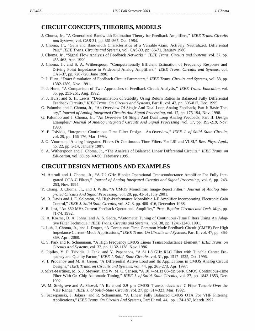
CIRCUIT CONCEPTS, THEORIES, MODELS J. Choma, Jr., “A Generalized Bandwidth Estimation Theory for Feedback Amplifiers,” IEEE Trans. Circuits
and Systems, vol. CAS-31, pp. 861-865, Oct. 1984. J. Choma, Jr., “Gain and Bandwidth Characteristics of a Variable -Gain, Actively Neutralized, Differential
Pair,” IEEE Trans. Circuits and Systems, vol. CAS-33, pp. 66-71, January 1986. J. Choma, Jr., “Signal Flow Analysis of Feedback Networks,” IEEE Trans. Circuits and Systems, vol. 37, pp.
455-463, Apr. 1990. J. Choma, Jr. and S. A. Witherspoon, “Computationally Efficient Estimation of Frequency Response and
Driving Point Impedance in Wideband Analog Amplifiers,” IEEE Trans. Circuits and Systems, vol. CAS-37, pp. 720-728, June 1990.
P. J. Hurst, “Exact Simulation of Feedback Circuit Parameters,” IEEE Trans. Circuits and Systems, vol. 38, pp. 1382-1389, Nov. 1991.
P. J. Hurst, “A Comparison of Two Approaches to Feedback Circuit Analysis,” IEEE Trans. Education, vol. 35, pp. 253-261, Aug. 1992.
P. J. Hurst and S. H. Lewis, “Determination of Stability Using Return Ratios In Balanced Fully Differential Feedback Circuits,” IEEE Trans. On Circuits and Systems, Part II, vol. 42, pp. 805-817, Dec. 1995.
G. Palumbo and J. Choma, Jr., “An Overview Of Single And Dual Loop Analog Feedback; Part I: Basic The-ory,” Journal of Analog Integrated Circuits And Signal Processing, vol. 17, pp. 175-194, Nov. 1998.
G. Palumbo and J. Choma, Jr., “An Overview Of Single And Dual Loop Analog Feedback; Part II: Design Examples,” Journal of Analog Integrated Circuits And Signal Processing , vol. 17, pp. 195-219, Nov. 1998.
Y. P. Tsividis, “Integrated Continuous-Time Filter Design––An Overview,” IEEE J. of Solid–State Circuits, vol. 29, pp. 166-176, Mar. 1994.
J. O. Voorman, “Analog Integrated Filters Or Continuous-Time Filters For LSI and VLSI,” Rev. Phys. Appl., no. 22, pp. 3-14, January 1987.
S. A. Witherspoon and J. Choma, Jr., “The Analysis of Balanced Linear Differential Circuits,” IEEE Trans. on Education, vol. 38, pp. 40-50, February 1995.
CIRCUIT DESIGN METHODS AND EXAMPLES M. Atarodi and J. Choma, Jr., “A 7.2 GHz Bipolar Operational Transconductance Amplifier For Fully Inte-
grated OTA-C Filters,” Journal of Analog Integrated Circuits and Signal Processing , vol. 6, pp. 243-253, Nov. 1994.
Y. Chang, J. Choma, Jr., and J. Wills, “A CMOS Monolithic Image-Reject Filter,” Journal of Analog Inte-grated Circuits And Signal Processing, vol. 28, pp. 43-51, July 2001.
W. R. Davis and J. E. Solomon, “A High-Performance Monolithic I-F Amplifier Incorporating Electronic Gain Control,” IEEE J. Solid State Circuits, vol. SC-3, pp. 408-416, December 1968.
S. R. Jost, “An 850 MHz Current Feedback Operational Amplifier,” Proc. Bipolar Circuits and Tech. Mtg ., pp. 71-74, 1992.
K. A. Kozma, D. A. Johns, and A. S. Sedra, “Automatic Tuning of Continuous-Time Filters Using An Adap-tive Filter Technique,” IEEE Trans. Circuits and Systems, vol. 38, pp. 1241-1248, 1991.
L. Luh, J. Choma, Jr., and J. Draper, “A Continuous Time Common Mode Feedback Circuit (CMFB) For High Impedance Current–Mode Applications,” IEEE Trans. On Circuits and Systems, Part II, vol. 47, pp. 363-369, April 2000.
C. S. Park and R. Schaumann, “A High Frequency CMOS Linear Transconductance Element,” IEEE Trans. on Circuits and Systems, vol. 33, pp. 1132-1138, Nov. 1986.
S. Pipilos, Y. P. Tsividis, J. Fenk, and Y. Papananos, “A Si 1.8 GHz RLC Filter with Tunable Center Fre-quency and Quality Factor,” IEEE J. Solid–State Circuits, vol. 31, pp. 1517-1525, Oct. 1996.
V. I. Prodanov and M. H. Green, “A Differential Active Load and Its Applications in CMOS Analog Circuit Designs,” IEEE Trans. on Circuits and Systems, vol. 44, pp. 265-273, Apr. 1997.
J. Silva-Martinez, M. S. J. Steyaert, and W. M. C. Sansen, “A 10.7–MHz 68–dB SNR CMOS Continuous-Time Filter With On-Chip Automatic Tuning,” IEEE J. of Solid–State Circuits, vol. 27, pp. 1843-1853, Dec. 1992.
W. M. Snelgrove and A. Shoval, “A Balanced 0.9–µm CMOS Transconductance–C Filter Tunable Over the VHF Range,” IEEE J. of Solid–State Circuits, vol. 27, pp. 314-323, Mar. 1992.
S. Szczepanski, J. Jakusz, and R. Schaumann, “A Linear Fully Balanced CMOS OTA For VHF Filtering Applications,” IEEE Trans. On Circuits And Systems, Part II: vol. 44, pp. 174-187, March 1997.

EE 402 USC Fall Semester 2003 J. Choma
vi
Z. Wang and W. Guggenbuhl, “A Voltage-Controllable Linear MOS Transconductor Using Bias Offset Tech-nique,” IEEE J. of Solid–State Circuits, vol. 25, pp. 315-317, Feb. 1990.
S. L. Wong, “Novel Drain–Based Transconductance Building Blocks for Continuous–Time Filter Applica-tions,” Electron. Lett., vol. 25, pp. 100-101, Jan. 1989.
A. Wyszynski, R. Schaumann, S. Szczepanski, and P. Van Halen, “Design of a 2.7 GHz Linear OTA and a 250-MHz Elliptic Filter in Bipolar Transistor-Array Technology,” IEEE Trans. On Circuits And Sys-tems, Part II: vol. 40, pp. 19-31, Jan. 1993.
5. Course Schedule
WEEK WEEK OF LECTURE TOPIC READINGS
1, 2 08/25/03 TWO PORT NETWORK MODELS & ANALYSIS Handout Notes 09/01/03 y–Parameter Model z–Parameter Model h–Parameter Model g–Parameter Model Transmission Parameters Indefinite Admittance Matrix Circuit Performance Open Loop Gain Loop Gain Closed Loop Gain Feedback Circuit Examples
3, 4 09/08/03 SCATTERING PARAMETERS Handout Notes 09/15/03 One Port Reflection Coeffic ient Chapter #11 Two Port Scattering Matrix I/O Reflection Coefficients Transducer Power Gain Feedback Parameter Relationship To Conventional Two Port Parameters Lossless Two Port Special Case
5 09/22/03 BIQUADRATIC FILTERS Chapter #7 Signal Flow Diagram Handout Notes Filter Examples Lowpass Bandpass Notch Generalized Biquadratic Architecture
6 09/29/03 FUNDAMENTALS OF FILT ER SYNTHESIS Chapter #1 Filters In Modern Integrated Circuits Fundamental Filter Build ing Blocks Tellegen’s Theorem Impedance And Admittance (Immittance) Functions Passive Immittances Positive Real Functions Scaling
7, 8, 9 10/06/03 FILTER APPROXIMATIONS Chapter #2 10/13/03 Butterworth Maximally Flat Magnitude 10/20/03 Chebyshev Equiripple Bessel Maximally Flat Delay Frequency Domain Transformations Lowpass -To- Highpass

EE 402 USC Fall Semester 2003 J. Choma
vii
WEEK WEEK OF LECTURE TOPIC READINGS
7, 8, 9 10/06/03 Lowpass -To- Bandpass 10/13/03 Design Examples Handout Notes 10/20/03 Butterworth Chebyshev Bessel
8 10/15/03 MIDTERM EXAMINATION Open Book
9 10/22/03 DESIGN PROJECT ASSIGNMENT
10, 11 10/27/03 RF MATCHING FILTERS Handout Notes 11/03/03 Review Of RLC Circuit Fundamentals Chapter #9 Up-Conversion Filter Down-Conversion Filter Broadband Matching Fundamental Considerations Equalizers Butterworth Broadband Constant Resistance Lattice
12, 13 11/10/03 DISTRIBUTED NETWORKS Handout Notes 11/17/03 Two Port Model Characteristic Impedance Attenuation Wavelength Lossless Examples Various Wavelengths Maximally Flat Delay
14, 15 11/24/03 ACTIVE DISTRIBUTED NETWORKS Handout Notes 12/01/03 Two Port Model Butterworth Bandpass Butterworth Notch
12/12/03 FINAL EXAMINATION (11:00 – 1:00) Open Book
Dr. John Choma, Professor and Chair Department of Electrical Engineering-Electrophysics 08 August 2003
cc. EE 402–F02 File Onder Oz
Related Documents

![Undergraduate Writing Assignments in Mechanical Engineering...Mechanical Engineering, Electrical and Computer Engineering, Biosystems Engineering, Civil Engineering and Design Engineering]](https://static.cupdf.com/doc/110x72/5ff7a06f83bfbd5c864bdc1a/undergraduate-writing-assignments-in-mechanical-engineering-mechanical-engineering.jpg)