UNIVERSITY OF OKLAHOMA GRADUATE COLLEGE MULTIPLIERLESS CSD TECHNIQUES FOR HIGH PERFORMANCE FPGA IMPLEMENTATION OF DIGITAL FILTERS A DISSERTATION SUBMITTED TO THE GRADUATE FACULTY in partial fulfillment of the requirements for the degree of Doctor of Philosophy By YUNHUA WANG Norman, Oklahoma 2007

Welcome message from author
This document is posted to help you gain knowledge. Please leave a comment to let me know what you think about it! Share it to your friends and learn new things together.
Transcript
UNIVERSITY OF OKLAHOMA
GRADUATE COLLEGE
MULTIPLIERLESS CSD TECHNIQUES FOR HIGH PERFORMANCE FPGA
IMPLEMENTATION OF DIGITAL FILTERS
A DISSERTATION
SUBMITTED TO THE GRADUATE FACULTY
in partial fulfillment of the requirements for the
degree of
Doctor of Philosophy
By
YUNHUA WANG Norman, Oklahoma
2007
UMI Number: 3283840
32838402008
UMI MicroformCopyright
All rights reserved. This microform edition is protected against unauthorized copying under Title 17, United States Code.
ProQuest Information and Learning Company 300 North Zeeb Road
P.O. Box 1346 Ann Arbor, MI 48106-1346
by ProQuest Information and Learning Company.
MULTIPLIERLESS CSD TECHNIQUES FOR HIGH PERFORMANCE FPGA IMPLEMENTATION OF DIGITAL FILTERS
A DISSERTATION APPROVED FOR THE SCHOOL OF ELECTRICAL AND COMPUTER ENGINEERING
BY
_____________________________ Dr. JOSEPH P. HAVLICEK, CHAIR
_____________________________ Dr. LINDA S. DEBRUNNER, CO-CHAIR
_____________________________
Dr. VICTOR E. DEBRUNNER
_____________________________
Dr. MURAD ÖZAYDIN
_____________________________ Dr. MONTE TULL

©Copyright by YUNHUA WANG 2007 All Rights Reserved.

iv
ACKNOWLEDGEMENTS
I would like to express my deepest gratitude to my advisor, Dr. Linda
DeBrunner, for her invaluable wisdom and encouragement. Her brilliant guidance,
patience and support motivate me to pursue challenges and inspire me to seek
higher understanding in my study. Her sincere friendship and kind help in my life is
such a blessing that will be hidden in my heart forever.
I am also grateful to my dissertation advisor, Dr. Joseph P. Havlicek, for his
great classes, for broadening my knowledge to image processing areas, for
reviewing my papers, dissertation and presentation slides, for the cheers-ups and
jokes.
I would also like to thank my committee members Dr. Victor DeBrunner,
for introducing me to this field, for reviewing my papers, for his time and kindly
sharing his knowledge. I also like to thank Dr. Monte Tull and Dr. Murad Özaydin
for their helpful questions, comments, and suggestions, and for their time and
sincere evaluation in this dissertation. Your assistance is highly appreciated.
I am very grateful to my dear family, my husband Dr. Dayong Zhou
providing a lot of love and concern. Also my girls DiDi Zhou, CoCo Zhou and baby
Joy, thanks for their sweet cooperation.

v
My appreciation also extends to all friends who have supported and assisted
me throughout the completion of my research.
Finally, I want to thank my parents for constant support of my life, thank
you for always being there!
Thank God — my heavenly father! Thank you for your love!
vi
TABLE OF CONTENTS
ACKNOWLEDGEMENTS .......................................................................................... iv
TABLE OF CONTENTS.............................................................................................. vi
LIST OF TABLES ........................................................................................................ ix
LIST OF FIGURES ..................................................................................................... xii
ABSTRACT................................................................................................................ xiv
Chapter 1 ........................................................................................................................ 1
Introduction............................................................................................... 1
1.1 Introduction to digital filters ................................................ 1
1.2 Problem statement................................................................ 5
1.3 Original contributions .......................................................... 9
1.4 Organization of the dissertation ......................................... 10
Chapter 2 ...................................................................................................................... 11
Overview of filter implementation techniques in FPGAs....................... 11
2.1 Introduction of filter implementation solutions ................. 11
2.2 FPGA DSP implementation issues .................................... 12
2.3 Current filter implementation techniques .......................... 13
2.4 Modified radix-4 Booth’s recoding multiplier................... 20
2.5 Multiplierless techniques in filter implementations........... 24
Chapter 3 ...................................................................................................................... 42
vii
A novel multiplierless hardware implementation method for adaptive filter
coefficients....................................................................................... 42
3.1 Introduction........................................................................ 42
3.2 New 2’s complement to CSD conversion method (FastCSD)
........................................................................................... 45
3.3 Comparison with Booth’s recoding and LUT techniques.. 57
Chapter 4 ...................................................................................................................... 60
A multiplier structure based on a novel real-time CSD recoding ........... 60
4.1 Introduction........................................................................ 60
4.2 Real-time CSD Multiplier Structure .................................. 62
4.3 Comparison with Booth’s recoding and other CSD recoding
techniques ......................................................................... 69
Chapter 5 ...................................................................................................................... 72
Extension topics ...................................................................................... 72
5.1 A multi-input CSD multiplier unit suitable for DSP algorithm
implementations................................................................ 72
5.2 Optimizing filter order and coefficient length in the design of
high performance filters for high throughput FPGA
implementations................................................................ 87
Chapter 6 .................................................................................................................... 104
Conclusions and future works............................................................... 104
viii
6.1 Conclusions...................................................................... 104
6.2 Future works .................................................................... 108
REFERENCES........................................................................................................... 110
APPENDIX A ............................................................................................................ 119
Nomenclatures and abbreviations ......................................................... 119
APPENDIX B ............................................................................................................ 122
Selected Matlab® codes........................................................................ 122
APPENDIX C ............................................................................................................ 127
Selected VHDL codes ........................................................................... 127
ix
LIST OF TABLES
TABLE 2.1 RADIX-4 MODIFIED BOOTH’S RECODING [27]........................................ 21
TABLE 2.2 CANONICAL RECODING [28] ................................................................. 27
TABLE 2.3 THE FIRST 13 SAMPLES MATLAB® SIMULATION RESULTS FOR LOOP
FILTER ................................................................................................... 39
TABLE 2.4 COMPLEXITY COMPARISON OF EXAMPLE LOOP FILTER WITH WORDLENGTH
OF 20 BITS.............................................................................................. 40
TABLE 2.5 FPGA IMPLEMENTATION COMPARISON OF EXAMPLE LOOP FILTER WITH
WORDLENGTH OF 20 BITS ...................................................................... 41
TABLE 3.1. THE TRUTH TABLE FOR MASK GENERATOR .......................................... 53
TABLE 3.2 PERFORMANCE ANALYSIS OF FASTCSD( × INDICATES THE MOST COSTLY
OPERATIONS IN EACH STEP. NOTE: STEP 2 AND STEP 3 CAN BE DONE
SIMULTANEOUSLY)................................................................................ 58
TABLE 4.1 RECODING SCHEME OF CSD ALGORITHM. ............................................ 64
TABLE 4.2 COMPLEXITY COMPARISON ON AVERAGE PERCENTAGE OF DATA IN THE
TRADITIONAL MULTIPLIER, RADIX-4 BOOTH’S RECODING MULTIPLIER,
SELF-TIMED CSD RECODING MULTIPLIER AND PROPOSED CSD RECODING
MULTIPLIER ........................................................................................... 71
TABLE 5.1 COMPLEXITY OF THE TRADITIONAL MULTIPLIER, CSD-ENCODED
MULTIPLIER, AND MULTI-INPUT CSD MULTIPLIER................................. 77
x
TABLE 5.2 QUANTIZATION AND FILTER OUTPUT ERROR POWER COMPARISON ....... 86
TABLE 5.3 THE RELATIONSHIP BETWEEN THE ORDER OF THE FILTER DESIGN AND THE
LENGTH OF THE QUANTIZED COEFFICIENTS (NOT INCLUDING THE SIGN BIT)
.............................................................................................................. 94
TABLE 5.4 THE RESULTS OF FILTER ORDER, WORDLENGTH OF COEFFICIENTS
REQUIRED, TOTAL NUMBER OF BINARY AND NONZERO CSD BITS, WHEN
STOPBAND ATTENUATION IS CHANGED (NOT INCLUDING THE SIGN BIT). 97
TABLE 5.5 COMPLEXITY COMPARISON OF MULTIPLIER-BASED AND MULTIPLIERLESS
ADAPTIVE FIR FILTERS OF ORDER N.................................................... 103
xi
LIST OF FIGURES
FIGURE 1.1 LMS ADAPTIVE FIR FILTER [3]. ............................................................ 5
FIGURE 2.1 MULTIPLY-ACCUMULATOR IMPLEMENTATION OF DIGITAL FILTER USING
SEQUENTIAL 2’S COMPLEMENT MULTIPLIER [27]. ................................ 15
FIGURE 2.2 SCHEMATIC DEPICTION OF A RIGHT-SHIFTING 2’S COMPLEMENT
ITERATIVE SHIFT/ADD MULTIPLIER [27]. .............................................. 16
FIGURE 2.3 CONSTANT COEFFICIENT MULTIPLIER (KCM) FILTER DESIGN [29]..... 18
FIGURE 2.4 DISTRIBUTED ARITHMETIC (DA) 4-TAP FIR FILTER DESIGN [30]. ....... 19
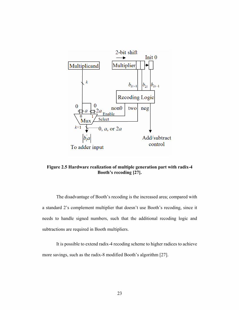
FIGURE 2.5 HARDWARE REALIZATION OF MULTIPLE GENERATION PART WITH
RADIX-4 BOOTH’S RECODING [27]. ...................................................... 23
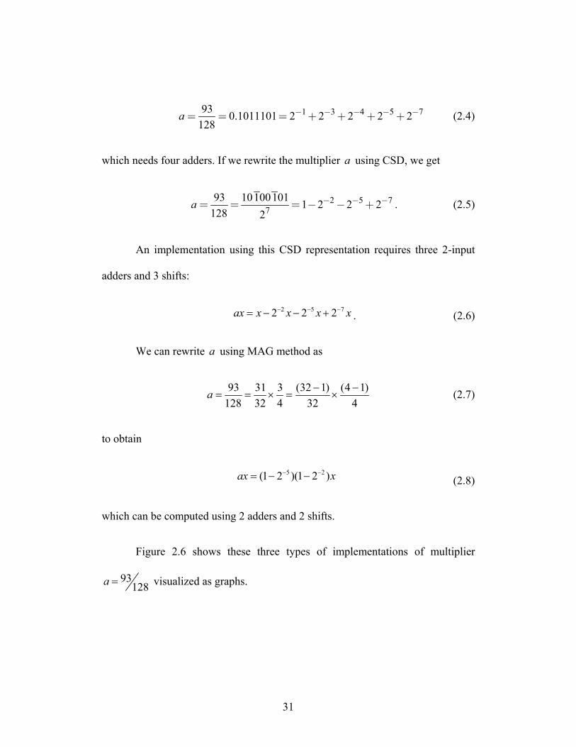
FIGURE 2.6 MULTIPLICATION BY 93128 USING (A) 2’S COMPLEMENT MULTIPLIER
WITH 4 ADDS/SUBTRACTORS; (B) CSD REPRESENTATION WITH 3
ADDS/SUBTRACTORS (C) MAG METHOD WITH 2 ADDS/SUBTRACTORS. 32
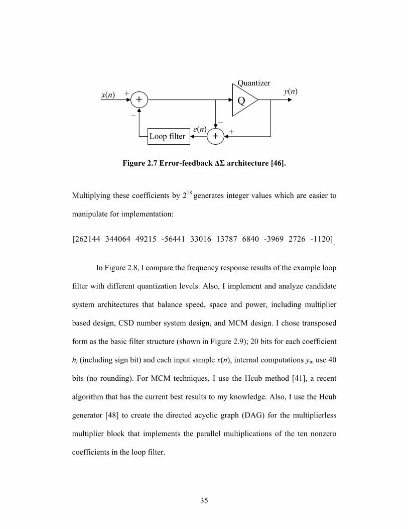
FIGURE 2.7 ERROR-FEEDBACK ΔΣ ARCHITECTURE [46]. ........................................ 35
FIGURE 2.8 FREQUENCY RESPONSES FOR DIFFERENT QUANTIZATION LEVELS OF
EXAMPLE 199 TAPS LOOP FILTER.......................................................... 36
FIGURE 2.9 THE FILTER STRUCTURE OF THE EXAMPLE 199 TAPS LOOP FILTER. ...... 37
FIGURE 2.10 HCUB ALGORITHM IMPLEMENTATION OF EXAMPLE LOOP FILTER WITH
NONZERO COEFFICIENTS SET {262144, 344064, 49215, -56441, 33016,
xii
13787, 6840, -3969, 2726, AND -1120}. .............................................. 38
FIGURE 2.11 THE ISE SIMULATION RESULTS OF LOOP FILTER (THE FIRST 13 SAMPLES
FROM 200). .......................................................................................... 40
FIGURE 3.1 BLOCK DIAGRAM FOR FASTCSD.......................................................... 47
FIGURE 3.2 THE IMPLEMENTATION OF THE MASK GENERATOR............................... 54
FIGURE 3.3 AN EXAMPLE OF NEW 2’S COMPLIMENT TO CSD CONVERSION PROCESS.
............................................................................................................. 56
FIGURE 4.1 IMPLEMENTATION OF MULTIPLE GENERATIONS AND SHIFT CONTROL PART
OF CSD RECODING MULTIPLIER IN LOGIC GATES.................................. 65
FIGURE 4.2 REAL-TIME CSD MULTIPLICATION BASED ON OUR NOVEL CSD RECODER.
............................................................................................................. 67
FIGURE 4.3 REAL-TIME CSD RECODER BLOCK DIAGRAM....................................... 68
FIGURE 5.1 DETAILED VIEW OF THE PROPOSED MULTIPLE-INPUT CSD MULTIPLIER
UNIT. .................................................................................................... 75
FIGURE 5.2 TRANSPOSED FORM FIR FILTER STRUCTURE........................................ 80
FIGURE 5.3 DIRECT FORM IIT IIR FILTER STRUCTURE............................................. 81
FIGURE 5.4 ADAPTIVE TRANSPOSED FORM FIR FILTER USING MULTIPLE-INPUT CSD
MULTIPLIER UNIT. ................................................................................ 82
FIGURE 5.5 USING THE PROPOSED MULTI-INPUT MULTIPLIER UNIT TO EFFICIENT
IMPLEMENT FIR FILTER BANKS. ........................................................... 85
FIGURE 5.6 FREQUENCY RESPONSES FOR DIFFERENT COEFFICIENT QUANTIZATION
xiii
LEVELS FOR THE 90TH ORDER LOW PASS FIR EXAMPLE FILTER (NOT
INCLUDING THE SIGN BIT IN BIT COUNTS). ............................................ 91
FIGURE 5.7 COEFFICIENT QUANTIZATION EFFECTS ON THE EXAMPLE FIR FILTER (NOT
INCLUDING THE SIGN BIT IN BIT COUNTS). ............................................ 92
FIGURE 5.8 THE EFFECTS ON FREQUENCY RESPONSE OF THE TRADEOFF BETWEEN
FILTER ORDER AND COEFFICIENT LENGTH. ........................................... 95
FIGURE 5.9 MSE FOR VARYING BIT LENGTHS USED PER COEFFICIENT (PLUS THE SIGN
BIT). ................................................................................................... 100
FIGURE 5.10 MSE FOR VARYING NUMBERS OF FILTER TAPS OF THE IDENTIFIED
SYSTEM WITH 11 BITS PER COEFFICIENT (INCLUDING THE SIGN
BIT, 52μ −= )...................................................................................... 100
FIGURE 5.11 PROPOSED STRUCTURE OF N+1 TAPS FIR ADAPTABLE FILTER. ...... 101
FIGURE 5.12 MSE FOR VARYING FILTER TAPS WHERE THE MULTIPLICATION IS A
SHIFT AND THE COEFFICIENTS IN THE IDENTIFIED SYSTEM HAVE 8 BITS
(INCLUDING THE SIGN BIT, 52μ −= ). .................................................. 102
xiv
ABSTRACT
Implementation of digital signal processing (DSP) algorithms in hardware,
such as field programmable gate arrays (FPGAs), requires a large number of
multipliers. Fast, low area multiply-adds have become critical in modern
commercial and military DSP applications. In many contemporary real-time DSP
and multimedia applications, system performance is severely impacted by the
limitations of currently available speed, energy efficiency, and area requirement of
an onboard silicon multiplier.
My research focus is on two key ideas for improving DSP performance:
1. Develop new high performance, efficient shift-add techniques
(“multiplierless”) to implement the multiply-add operations without the
need for a traditional multiplier structure.
2. There is a growing trend toward design prototyping and even
production in FPGAs as opposed to dedicated DSP processors or ASICs;
leverage this trend synergistically with the new multiplierless structures
to improve performance.
My work is based on a dramatic new technique for converting between 2’s
complement and CSD number systems, and results in high-performance structures
xv
that are particularly effective for implementing adaptive systems in reconfigurable
logic.
Adaptive system implementations require real-time conversion of
coefficients to Canonical Signed Digit (CSD) or similar representations to benefit
from multiplierless techniques for implementing filters. Multiplierless approaches
are used to reduce the hardware and increase the throughput. This dissertation
introduces the first non-iterative hardware algorithm to convert 2’s complement
numbers to their CSD representations (FastCSD) using a fixed number of shift and
logic operations. As a result, the power consumption and area requirements
required for hardware implementation of DSP algorithms in which the coefficients
are not known a priori can be greatly reduced. Because all CSD digits are produced
simultaneously, the conversion speed and thus the throughput are improved when
compared to overlap-and-scan techniques such as Booth’s recoding.
I leverage FastCSD to develop a new, high performance iterative
multiplierless structure based on a novel real-time CSD recoding, so that more zero
partial products are introduced. Up to 66.7% zero partial products occur compared
to 50% in the traditional modified Booth’s recoding. Also, this structure reduces
the non-zero partial products to a minimum. As a result, the number of arithmetic
operations in the carry-save structure is reduced. Thus, an overall speed-up, as well
as low-power consumption can be achieved. Furthermore, because the proposed
xvi
structure involves real time CSD recoding and does not require a fixed value for the
multiplier input to be known a priori, the proposed multiplier can be applied to
implement digital filters with non-fixed filter coefficients, such as adaptive filters.
I also introduce a new multi-input Canonical Signed Digit (CSD) multiplier
unit, which requires fewer shift/add/subtract operations and reduced CSD number
conversion overhead compared to existing techniques. This results in reduced
power consumption and area requirements in the hardware implementation of DSP
algorithms. Furthermore, because all the products are produced simultaneously, the
multiplication speed and thus the throughput are improved. The multi-input
multiplier unit is applied to implement digital filters with non-fixed filter
coefficients, such as adaptive filters. The implementation cost of these digital filters
can be further reduced by limiting the wordlength of the input signal with little or
no sacrifice to the filter performance, which is confirmed by my simulation results.
The proposed multiplier unit can also be applied to other DSP algorithms, such as
digital filter banks or matrix and vector multiplications.
Finally, the tradeoff between filter order and coefficient length in the design
and implementation of high-performance filters in Field Programmable Gate
Arrays (FPGAs) is discussed. Non-minimum order FIR filters are designed for
implementation using Canonical Signed Digit (CSD) multiplierless
implementation techniques. By increasing the filter order, the length of the

xvii
coefficients can be decreased without reducing the filter performance. Thus, an
overall hardware savings can be achieved.
1
Chapter 1
INTRODUCTION
1.1 Introduction to digital filters
Digital filters are among the most significant components in DSP
applications. Often, DSP algorithms are implemented using general purpose DSP
processors. Although those DSP processors typically have high-speed multiply and
accumulator circuits, only a limited number of operations can be performed before
the next sample arrives, thereby limiting the bandwidth.
VLSI based filters including those using FPGAs and ASICs, are
implemented with a parallel-pipelined architecture, enhancing the overall
performance. For high-performance applications, VLSI implementations provide
better device utilization through conservation of board space and system power
consumption, which is an important advantage not available with many stand-alone
DSP chips. Digital filter implementation in FPGAs and other VLSI
implementations allows for higher sampling rates and lower cost than that available
2
from traditional DSP chips [1].
Finite impulse response (FIR) filters are widely used in many digital signal
processing application areas such as communications and signal preconditioning.
Many important properties make FIR filters attractive, such as simple structure,
easily achieved linear-phase performance and pipelined design. FIR filter operation
can be represented by the following equation [2]:
1 1
0 0
( ) ( ) ( )M M
kk k
k k
y n h x n k H z h z− −
−
= =
= − ⇔ =∑ ∑ (1.1)
where M is the filter length and the kh are the filter coefficients.
The basic structures of FIR filters can be classified into several major forms:
direct form, cascade form, polyphase, lattice, etc.
An infinite impulse response (IIR) filter is a recursive filter in which the
current output depends on previous outputs as well as inputs. To meet certain
specifications, an IIR filter can often be much more efficient in terms of order
compared to an FIR filter. The main drawbacks of IIR filters are that potential
instability can be introduced by feedback, limit cycles may occur, phase response is
typically non-linear and it is hard to implement in a pipelined design.
The basic IIR equation is given by [2]:
3
1
1 0
( ) ( ) ( )N M
k kk k
y n a y n k b x n k−
= =
=− − + −∑ ∑ (1.2)
with the direct form transform function
1 1
0 1 11
1( )
1
MM
NN
b b z b zH za z a z
− −−
−
+ + +=
+ + + (1.3)
where M is the maximum input delay, the bk are the numerator coefficients; N is
the maximum output delay, and the aj are the denominator coefficients.
Adaptive filters have achieved widespread acceptance and are included in
many digital signal processing application areas. Whenever there are situations
where the prescribed specifications are not available, or are time-varying, a digital
filter with adaptive coefficients, known as an adaptive filter, is employed as the
solution. These situations include applications such as system identification, active
noise control (ANC), and others [3].
Adaptive filters automatically adjust their coefficients to get the best results
according to some objective function. The objective function yields a coefficient
update (learning) algorithm. The choice of the algorithm is generally the most
crucial aspect of the overall adaptive process. In this dissertation, I would like to
introduce the Least Mean Square (LMS) update method [3]. This algorithm is
widely used in various applications of adaptive filtering due to its computational
4
simplicity. This solution uses an approximation to the gradient in the direction that
obtains the minimum mean square error (MSE).
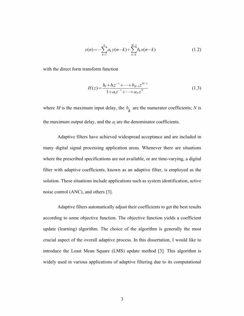
A general block diagram of a LMS adaptive filter is illustrated in Figure 1.1
[3], where estimation error ( )e n is:
( ) ( ) ( )e n d n y n= − (1.4)
where n is the iteration number, ( )d n is desired output and ( )y n is filter output.
Then, the tap-coefficient adaptation equation is given by:
( )( )
( )
( )( )
( )
( )
( )( )
( )
0 0
1 1
11 1
1N N
w n w n x nw n w n x n
e n
w n w n x n N
μ
+⎡ ⎤ ⎡ ⎤ ⎡ ⎤⎢ ⎥ ⎢ ⎥ ⎢ ⎥+ −⎢ ⎥ ⎢ ⎥ ⎢ ⎥= +⎢ ⎥ ⎢ ⎥ ⎢ ⎥⎢ ⎥ ⎢ ⎥ ⎢ ⎥
+ −⎢ ⎥ ⎢ ⎥ ⎢ ⎥⎣ ⎦ ⎣ ⎦ ⎣ ⎦
(1.5)
where ( )x n represents the input signal, μ denotes gradient step size, and ( )kw n is
the vector of time-varying filter coefficients.
The filter output ( )y n can be written:
( ) ( ) ( ) ( )0 1 1 Ny n w x n w x n w x n N= + − + + − . (1.6)
The learning error ( )e n is computed based on the desired output ( )d n as
shown in (1.4). This error is used to update the time-varying FIR filter coefficients
5
as in (1.5). Then, the filter output ( )y n is calculated as in (1.6) above. It is, of
course, the convolution of the input ( )x n with the FIR time-varying filter
coefficients ( ).kw n In all practical applications, this loop is computed repeatedly.
The gradient step size, µ, is chosen carefully to ensure convergence (not too large)
without being so conservative (not too small) that the learning rate is too slow.
Figure 1.1 LMS adaptive FIR filter [3].
The basic structures for adaptive filtering can be classified into FIR
adaptive filters and IIR adaptive filters.
1.2 Problem statement
Implementation of digital signal processing (DSP) algorithms and
W ( )x n ( )y n
Adaptation Algorithm
( )d n+( )e n
−
6
multimedia applications in hardware, such as field programmable gate arrays
(FPGAs) and digital signal processors, requires a large number of multiplications.
Fast, low area multiply-adds are critical in DSP implementations in modern
commercial and military DSP applications.
In many contemporary real-time DSP and multimedia applications, system
performance is severely impacted by the limitations of currently available speed,
energy efficiency, and area requirement of an onboard silicon multiplier. This is
exacerbated in handheld multimedia devices due to the small size and limited
battery lifetimes. Therefore, there has been a lot of research carried out on the
development of advanced multiplier techniques to reduce the energy consumption,
area requirements, and/or computation time, e.g. [4]-[12].
My research in this dissertation is focused on the implementation of
adaptable algorithms in DSP applications. Such as, adaptive filters, Active Noise
Control (ANC) etc.. The coefficients of an adaptive filter change with time. These
filters can automatically adjust their coefficients to get the best result according to
some objective function. The objective function yields a coefficient update
(learning) algorithm. For real-time implementation of digital filters, parallel
implementation of the multiplications is typically required. Many researchers have
addressed the question of how to implement the multiplications for
fixed-coefficient filters. Recently there has been a renewed interest in
7
adaptable-coefficient filters [6], [8], [13]. In general, there is a tradeoff between the
hardware complexity and the filter performance associated with the wordlength of
the multipliers (usually coefficients). Increased coefficient wordlength increases
implementation complexity, and decreased coefficient wordlength results in
greater filter response error. In fixed coefficient filters, multiplierless techniques
are sometimes implemented by encoding the coefficients in Canonical Signed Digit
(CSD) number system [14] or Signed Power of Two (SPT) representation [8].
Further improvement can be achieved by using dependence-graph algorithms, such
as Multiplier Adder Graph (MAG) [15] or Bull-Horrocks’ algorithm [16]. Most of
those approaches cannot be applied to real-time implementation of adaptive and
non-fixed coefficient systems; e.g., LUT and dependence-graph algorithms which
require the value of the filter coefficients to be known a priori. Some researchers
have considered techniques for implementing adaptive filters that use specialized
encoding of the inputs. CSD coding of coefficients for adaptive filters has been
proposed [6], and non-uniform quantization of inputs has been considered [17].
In this dissertation, I consider the case of adaptive filters in which the filter
coefficients cannot be known a priori. To decrease the implementation complexity
without increasing the filter response error, developing new time and space
efficient techniques for high performance FPGA implementation of adaptive and
non-fixed coefficient digital filters become critical, which include new algorithm to
convert 2’s complement to CSD and new high performance “multiplierless”
8
multiply-add structures.
The result of my research will be new multiply-add algorithms and
architectures providing
• Significantly reduced space complexity
• Significantly reduced time complexity
• Significantly reduced power consumption
compared to the current state of the art.
Many modern DSP processors are optimized for floating point coefficients;
the new techniques developed in this dissertation provide a performance advantage
for fixed point filter implementations. Thus, the techniques developed here are
more appropriate for FPGA implementations.
The new techniques developed in this dissertation are particularly well
suited for implementing high speed adaptive filters implementations where
adaptation can be applied in both the coefficient values and their word lengths. This
fits well with the reconfigurable hardware capabilities available in an FPGA
implementation as opposed to ASIC or dedicated DSP processor.
9
1.3 Original contributions
This dissertation makes the following contributions:
• Developed the first non-iterative hardware algorithm to convert 2’s
complement to CSD (FastCSD) [18].
• Faster than almost all existing techniques
• Lower space complexity
• Lower power consumption
• Leveraged FastCSD [18] to develop a new, high performance iterative
multiplier structure based on novel real-time CSD recoding [19], [20],
which has simpler structure than other competitive techniques with less
computational complexity and low power consumptions.
• Compared with other CSD multipliers: faster, smaller, better power
efficiency and/or flexibility
• Compared to traditional array multipliers: lower area, lower power
consumption
• Compared to traditional iterative multipliers: faster, lower power
consumption
10
• Developed the first multi-input multiplier unit suitable for adaptive DSP
algorithm implementations [21].
• Optimized filter order and coefficient length for design of high performance
FIR filters [22].
1.4 Organization of the dissertation
This dissertation will be organized as follows. The first chapter provides
some introductory discussion. The second chapter provides an overview of filter
implementation techniques in FPGAs. I review some common filter design
techniques, and then multiplierless techniques in filter design are introduced. A
novel hardware implementation method for adaptive filter coefficients and a
multiplier structure based on a novel real-time CSD recoding will be studied and
developed in Chapter 3 and Chapter 4, respectively. In Chapter 5, I consider two
extension topics, the first is a multi-input multiplier unit suitable for adaptive DSP
algorithm implementations; the other one is a method that optimizes filter order and
coefficient length in the design of high performance filters for high throughput
FPGA implementations. In Chapter 6, I summarize my contributions and outline
areas for future work.
11
Chapter 2
OVERVIEW OF FILTER IMPLEMENTATION
TECHNIQUES IN FPGAS
2.1 Introduction of filter implementation solutions
Digital Signal Processing (DSP) is one of the most active areas in VLSI
research and development [2]. Traditionally, DSP algorithms are implemented
either using general purpose DSP processors [23] or using Application Specific
Integrated Circuits (ASICs) [24]. Although DSP processors are less expensive and
flexible, they have the disadvantage of low speed. The applications of those
processors are limited since many DSP applications require high speed and high
throughput. On the other hand, ASICs which are high speed, but expensive and less
flexible, cannot satisfy the needs of all designers.
An FPGA is a network of reconfigurable hardware with reconfigurable
interconnects that can be easily programmed, which provides solutions that
maintain both the advantages of the approach based on DSP processors and the
approach based on ASICs [25], [26]. An integrated chip designer can use an FPGA
12
to dynamically design a chip, test it, reconfigure it, and settle on a design that can
then be used to manufacture an ASIC. The major advantages of FPGAs are
• Versatility
• Flexibility
• Huge performance gain for some applications
• Re-useable hardware designs
2.2 FPGA DSP implementation issues
Based on the advantages above, many DSP algorithms, such as FFTs, FIR
or IIR filters, to name just a few, previously built with ASICs or DSP processors,
are now routinely replaced by FPGAs [1]. Also, some recent FPGAs include DSP
features [25], such as ALTERA® Stratex and XILINX® Virtex II, which makes
FPGAs more attractive for DSP algorithm implementations.
There is a growing trend toward design prototyping and even production in
FPGAs as opposed to dedicated DSP processors or ASICs. I leverage this trend
synergistically with the new multiplierless structures to further improve the
performance.
13
The reasons for me to choose FPGA as the design platform are listed here.
First of all, the new techniques developed in this dissertation provide a
performance advantage for fixed point filter implementations. Many modern DSP
processor are optimized for floating point coefficients [24]; thus the techniques
developed here are more appropriate for FPGA implementations [25].
Secondly, the new techniques developed in this dissertation are particularly
well suited for implementing adaptive filters. Adaptation can be applied in both the
coefficient values and their word lengths. This fits well with the reconfigurable
hardware capabilities available in an FPGA implementation as opposed to ASIC or
dedicated DSP processor [25].
Finally, the new techniques developed in this dissertation are particularly
well suited for high speed FPGA implementations as opposed to DSP processor
[25].
2.3 Current filter implementation techniques
The most common filter implementation approaches are multiplier-based
design and LUT-based design [27].
14
2.3.1 Multiplier-Based design
To better understand multiplier based design techniques, let us discuss the
characteristics of the multiplier first. Multiplication involves two basic operations:
generation of partial products and accumulation of partial products. Hence, all
techniques for speeding up multiplication can be categorized into to two main
groups: those that seek to reduce the number of nonzero partial products and those
that seek to accelerate the accumulation of partial products [27].
There are three types of multipliers: sequential/iterative multipliers, parallel
multipliers and array multipliers [28]. Sequential multipliers, also called iterative
multipliers in some literature, generate partial products sequentially and add each
newly generated product to previously accumulated partial products. The major
properties for this type of multipliers are small area consumption, reduced pin
count and wire length, and high clock rate but low speed. Parallel multipliers
generate partial products in parallel and accumulate them using a fast
multi-operand adder. Using this type of multiplier, the execution speed is increased
by sacrificing area. An array of identical cells generates new partial products and
accumulates them simultaneously in an array multiplier, such that no separate
circuits are required for generation and accumulation; in this way, execution time is
reduced, but hardware complexity is increased [28].
Here, let’s study the basic idea of multiplication by considering a sequential
15
fixed-width 2’s complement multiplier as an example. Suppose inputs and
coefficients are all n-bit wide, then the product will be 2n-bit wide. Often, the
product will be quantized to n-bits by eliminating the n Least Significant Bits
(LSBs). This approach can reduce area consumption, but rounding error is
introduced. When it is applied to basic Multiply-Accumulator (MAC) filter design
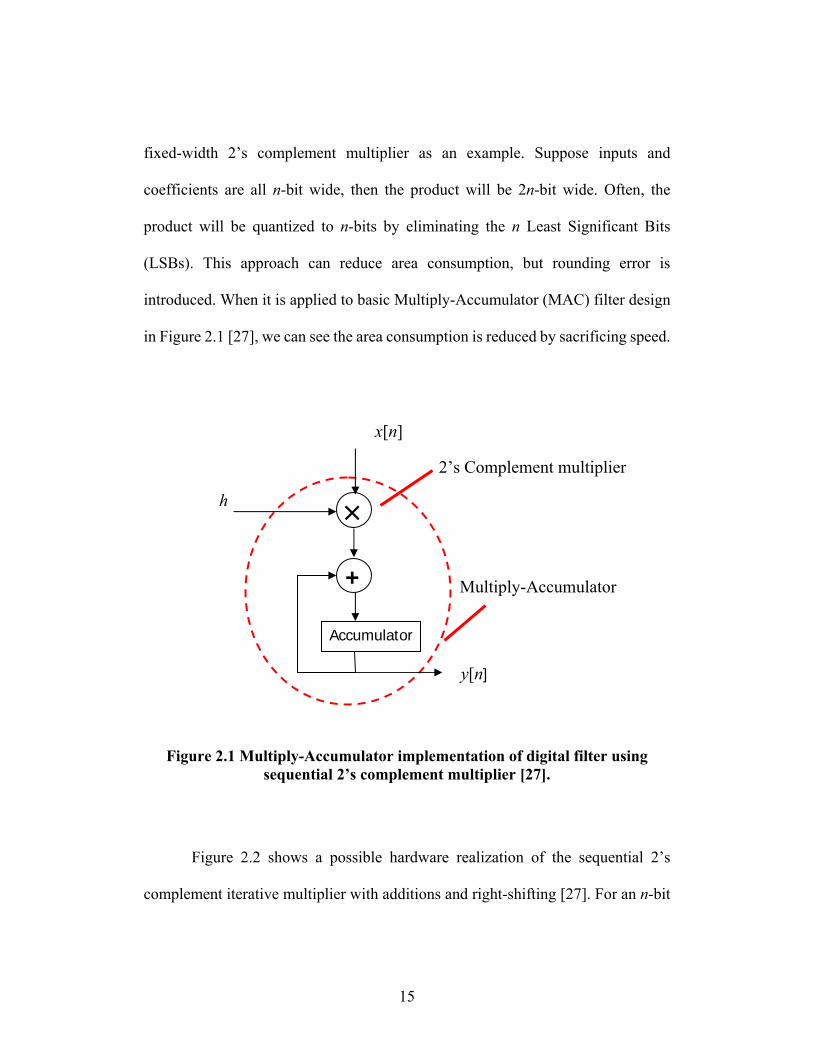
in Figure 2.1 [27], we can see the area consumption is reduced by sacrificing speed.
Figure 2.1 Multiply-Accumulator implementation of digital filter using sequential 2’s complement multiplier [27].
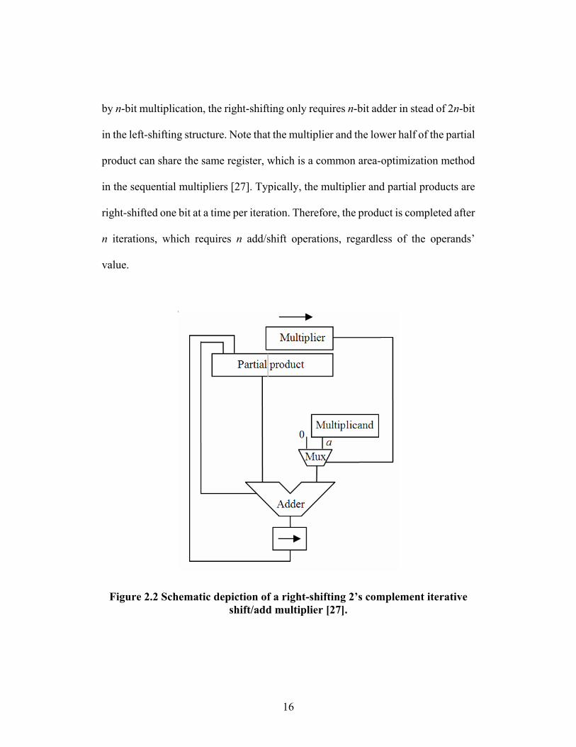
Figure 2.2 shows a possible hardware realization of the sequential 2’s
complement iterative multiplier with additions and right-shifting [27]. For an n-bit
+
×
Accumulator
h
x[n]
y[n]
Multiply-Accumulator
2’s Complement multiplier
16
by n-bit multiplication, the right-shifting only requires n-bit adder in stead of 2n-bit
in the left-shifting structure. Note that the multiplier and the lower half of the partial
product can share the same register, which is a common area-optimization method
in the sequential multipliers [27]. Typically, the multiplier and partial products are
right-shifted one bit at a time per iteration. Therefore, the product is completed after
n iterations, which requires n add/shift operations, regardless of the operands’
value.
Figure 2.2 Schematic depiction of a right-shifting 2’s complement iterative shift/add multiplier [27].
17
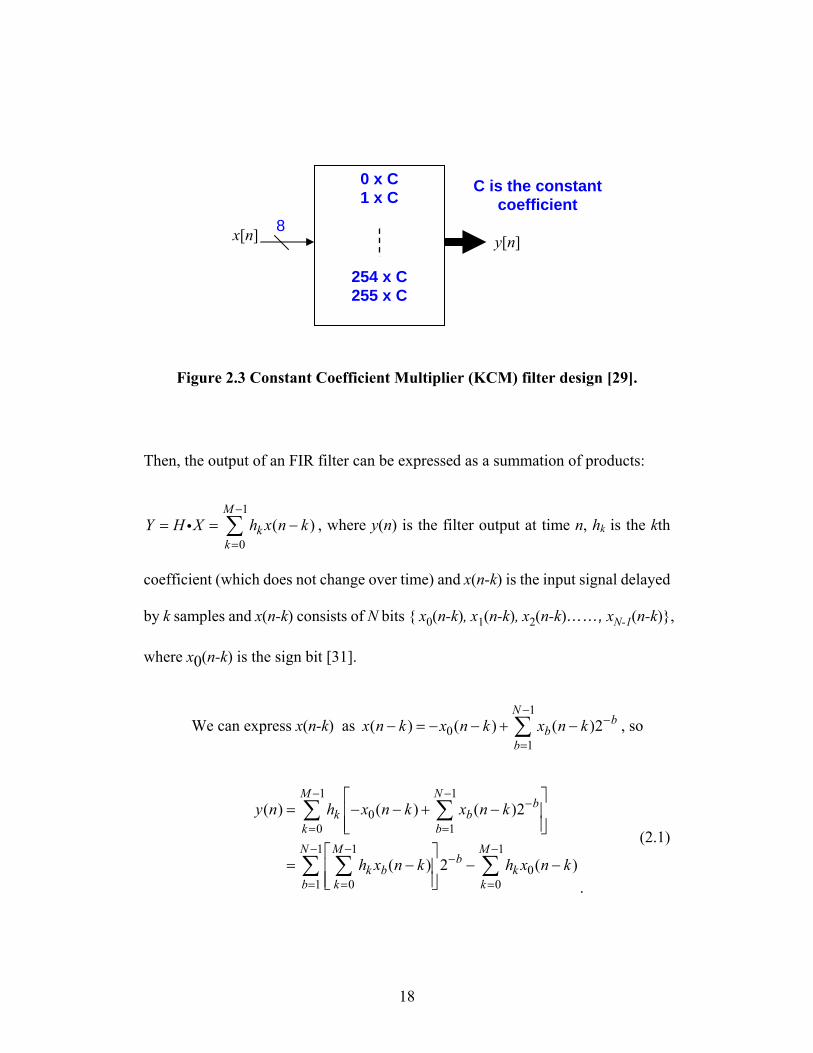
2.3.2 LUT-based design
Another commonly used technique in FPGA design is the Look-Up-Table
(LUT) [29]. Many algorithms used in DSP, such as filtering, are based on constant
coefficient values. Usually for the multipliers involved in these types of algorithms,
output purely depends on the input data. Thus, a Look-Up-Table can be used to
implement the multiplier by storing pre-computed partial products of the fixed
coefficient in distributed ROM to reduce the logic cost. This kind of design
technique includes Constant Coefficient Multiplier (KCM) (see Figure 2.3) [29]
and Distributed Arithmetic (DA) approaches [30].
An advantage of LUT architectures is that they simplify timing of
synchronous logic, so they are fast. However, the disadvantage is an unusually
large number of memory cells required to implement some designs, as in the case
when the number of inputs is large, which requires much area. Also, the
multiplier’s wordlength usually is fixed and the value of multiplier should be
known ahead of time [29].
Another Look-Up-Table based design is Distributed Arithmetic which is
used to design bit-level architectures for vector-vector multiplications based on
saving partial products in memories [30]. Because the coefficients are known ahead
of time, it is possible to pre-calculate the result of a multiplication. FIR filter can be
presented as a product of two length-M vectors H (coefficients) and X (inputs).
18
Figure 2.3 Constant Coefficient Multiplier (KCM) filter design [29].
Then, the output of an FIR filter can be expressed as a summation of products:
1
0( )
M
kk
Y H X h x n k−
== = −∑i , where y(n) is the filter output at time n, hk is the kth
coefficient (which does not change over time) and x(n-k) is the input signal delayed
by k samples and x(n-k) consists of N bits { x0(n-k), x1(n-k), x2(n-k)……, xN-1(n-k)},
where x0(n-k) is the sign bit [31].
We can express x(n-k) as 1
01
( ) ( ) ( )2N
bb
bx n k x n k x n k
−−
=− = − − + −∑ , so
1 1
00 11 1 1
01 0 0
( ) ( ) ( )2
( ) 2 ( )
M Nb
k bk bN M M
bk b k
b k k
y n h x n k x n k
h x n k h x n k
− −−
= =
− − −−
= = =
⎡ ⎤= − − + −⎢ ⎥
⎢ ⎥⎣ ⎦⎡ ⎤
= − − −⎢ ⎥⎢ ⎥⎣ ⎦
∑ ∑
∑ ∑ ∑.
(2.1)
x[n] y[n]8
0 x C 1 x C
254 x C 255 x C
C is the constant coefficient
19
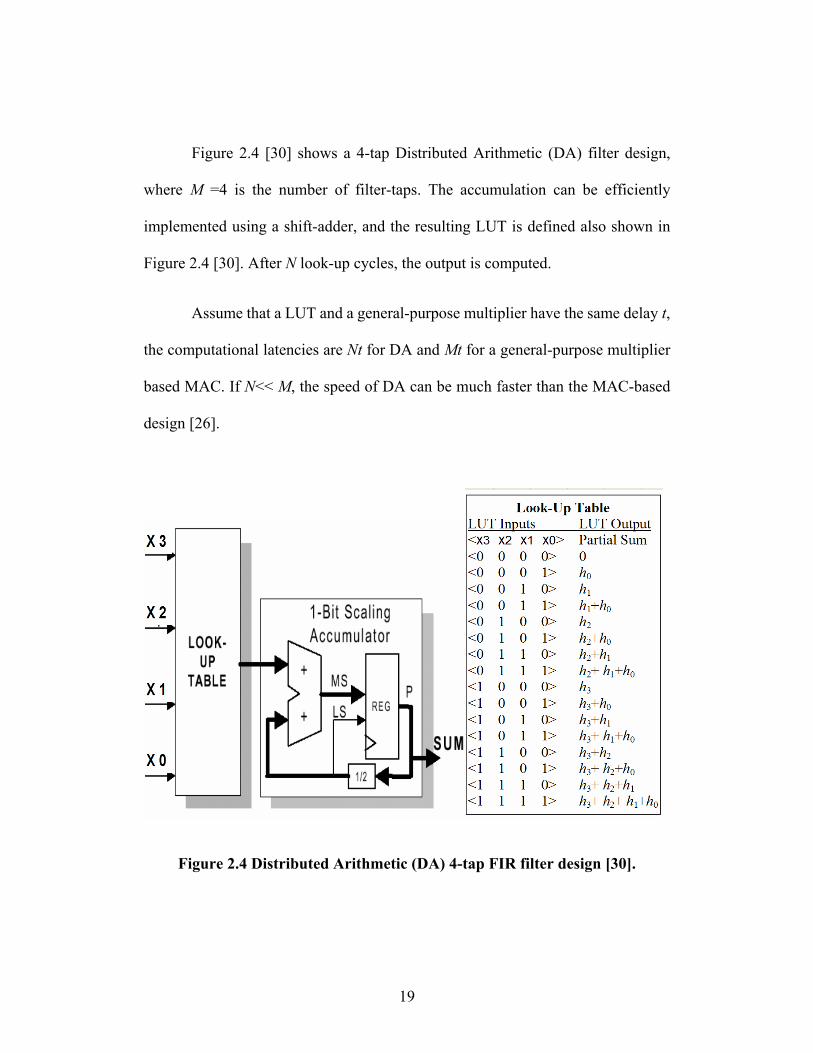
Figure 2.4 [30] shows a 4-tap Distributed Arithmetic (DA) filter design,
where M =4 is the number of filter-taps. The accumulation can be efficiently
implemented using a shift-adder, and the resulting LUT is defined also shown in
Figure 2.4 [30]. After N look-up cycles, the output is computed.
Assume that a LUT and a general-purpose multiplier have the same delay t,
the computational latencies are Nt for DA and Mt for a general-purpose multiplier
based MAC. If N<< M, the speed of DA can be much faster than the MAC-based
design [26].
Figure 2.4 Distributed Arithmetic (DA) 4-tap FIR filter design [30].
20
2.4 Modified radix-4 Booth’s recoding multiplier
Booth’s recoding is a tricky way to reduce the number of partial products in
a binary multiplier [12]. The basic idea is to replace additions arising from a string
of ones with a single subtraction at rightmost in a run of ones, then add back a one
before the leftmost one in the run based on:
1 1 12 2 2 2 2 2j j i i j i− + ++ + + + = − (2.2)
The longer the sequence of 1s, the larger savings can be achieved, for
example, number “0011110” is recoded by “01000 1 0”. Therefore, many zero
partial products are generated. However, the original proposed Booth’s recoding
algorithm can only speed up multiplication when a multiplier has many consecutive
1’s, and Booth’s recoding becomes very inefficient when a multiplier has
alternative 1 and 0’s, e.g. the number “010101” is represented by “1 1 1 1 1 1 ”,
requiring more add/shift operations.
The radix-4 modified Booth’s recoding algorithm has been widely used in
modern high-speed multiplication circuits [32]. Using a modified Booth algorithm,
sequential 3-bit segments of a 2’s complement number are converted into the digit
set{ }2, 1, 0± ± . This technique reduces an n-bit 2’s complement multiplier to
2n⎡ ⎤⎢ ⎥ digits. The number of partial products has been reduced to n/2 which can be
readily calculated by shift/add/subtract operations, such that these multipliers can
21
achieve about 40% reduction in area and power consumption [27].
The radix-4 modified Booth’s recoding is performed by the scheme shown
in Table 2.1 [27]. The 2’s complement number b is converted to b', where the digit
bi' of the Booth’s recoded number b' is obtained from the three digits b2i+1, b2i and
b2i-1 of a 2’s complement number b, a is the multiplicand.
TABLE 2.1 RADIX-4 MODIFIED BOOTH’S RECODING [27]
b2i +1 b2i b2i-1 'ib Operation
0 0 0 0 +0
0 0 1 1 +a
0 1 0 1 +a
0 1 1 2 +2a
1 0 0 -2 -2a
1 0 1 -1 -a
1 1 0 -1 -a
1 1 1 0 0
22
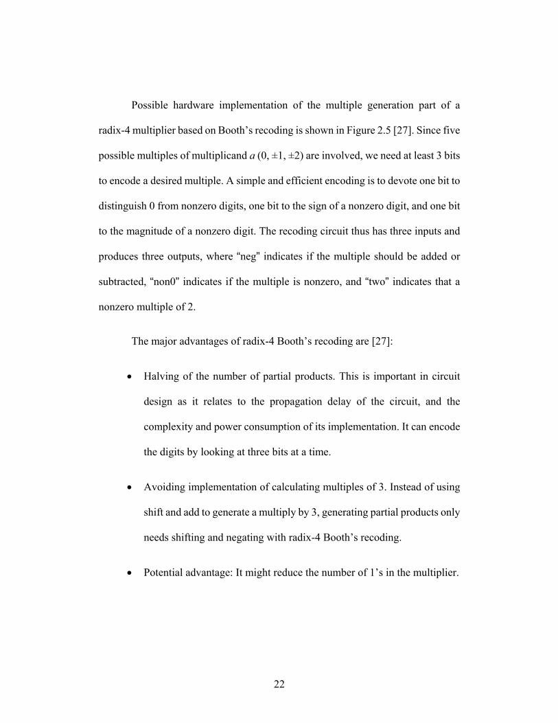
Possible hardware implementation of the multiple generation part of a
radix-4 multiplier based on Booth’s recoding is shown in Figure 2.5 [27]. Since five
possible multiples of multiplicand a (0, ±1, ±2) are involved, we need at least 3 bits
to encode a desired multiple. A simple and efficient encoding is to devote one bit to
distinguish 0 from nonzero digits, one bit to the sign of a nonzero digit, and one bit
to the magnitude of a nonzero digit. The recoding circuit thus has three inputs and
produces three outputs, where “neg” indicates if the multiple should be added or
subtracted, “non0” indicates if the multiple is nonzero, and “two” indicates that a
nonzero multiple of 2.
The major advantages of radix-4 Booth’s recoding are [27]:
• Halving of the number of partial products. This is important in circuit
design as it relates to the propagation delay of the circuit, and the
complexity and power consumption of its implementation. It can encode
the digits by looking at three bits at a time.
• Avoiding implementation of calculating multiples of 3. Instead of using
shift and add to generate a multiply by 3, generating partial products only
needs shifting and negating with radix-4 Booth’s recoding.
• Potential advantage: It might reduce the number of 1’s in the multiplier.
23
Figure 2.5 Hardware realization of multiple generation part with radix-4 Booth’s recoding [27].
The disadvantage of Booth’s recoding is the increased area; compared with
a standard 2’s complement multiplier that doesn’t use Booth’s recoding, since it
needs to handle signed numbers, such that the additional recoding logic and
subtractions are required in Booth multipliers.
It is possible to extend radix-4 recoding scheme to higher radices to achieve
more savings, such as the radix-8 modified Booth’s algorithm [27].
24
2.5 Multiplierless techniques in filter implementations
As we know multipliers are the most expensive building blocks in terms of
silicon area and throughput in digital filter implementations. Thus, a great effort
has been made to speed up and simplify the multiplication [4]-[12]. Many
researchers have addressed this problem by restricting the coefficient wordlength,
or by quantizing filter coefficients to the limit number of power-of-two [33]-[35].
In these cases, a conventional multiplier is avoided altogether [36]. Multiplications
can be replaced by simple shift and add operations [36]. This results in
multiplierless techniques. Instead of traditional multiply-add implementations,
these multiplierless techniques use the knowledge that multiplication by a
power-of-two can be simply obtained by shifting the data bus by the appropriate
number of bits. Thus, filter coefficients can be realized by incorporating a few
adders (or subtractors) and bit shifters. The bit shifters are implemented by
choosing the appropriate interconnections [37]. The number of add/shift operations
is directly related to the power consumption and area required, and it depends on
the number of 1’s in the multiplier.
Usually, multiplierless techniques are divided into alternate number
representations and constant multiplication problems. As we discussed in section
2.3.1, there are two ways to speed up multiplication. One is by reducing the number
of operands (partial products) to be added; the other is by adding the operands
25
faster (accelerating accumulation) [27]. Most multiplierless techniques make use of
all the essences of the above two categories, since filter coefficients are realized by
the limit number of power-of-two, and thus, the number of operands to be added is
significantly reduced. At the same time, only simple shift and add/subtract
operations are involved in most multiplierless techniques, the resultant increase in
speed is also huge [36].
2.5.1 Alternate number representations
Further benefits can be achieved by considering alternate number
representations, such as the Canonical Signed Digit (CSD) number system [14] or
Signed Power of Two (SPT) representation [8] and Minimal Signed Digit (MSD)
[38].
2.5.1.1 Canonical Signed Digit (CSD)
CSD representation [39] is a radix-two number system with digit set
{ 1, 0, 1}− that has the “canonical” property that no two consecutive bits in the
CSD number are nonzero and the possible number of nonzero bits in a CSD number
is minimal [14]. For example, the 2’s complement number
26
10101101 01010101x= = , where “ 1 ” stands for “-1”. This representation
replaces the additions arising from a string of ones in a binary number with a single
subtraction, so that the “shift-and-add” algorithm becomes “shift-and-add/subtract”,
i.e. a multiplier can be realized by incorporating a few adders (or subtractors) and
bit shifters. CSD numbers have proven to be useful in implementing multiplierless
multiplication with reduced complexity, because the cost of multiplication is a
direct function of the number of nonzero bits in the multiplier, which can be
reduced by using CSD representation. It is shown in [9] that the probability that a
CSD digit jc has a nonzero value is given by
( 1) 1 3 (1 9 )[1 ( 1 2) ]njP c n= = + − − (2.3)
where n is the number of bits in the representation.
As n becomes large, the probability tends towards 1/3, and we see that for
an n-bit CSD multiplier, the number of add/subtract operations never exceeds n/2
and can be reduced to n/3 on average, as the wordlength of multiplier grows [14].
To benefit from the CSD implementation advantages, the conversion of
numbers from 2’s complement to CSD format must be implemented in hardware.
Many researchers have addressed the question of how to convert 2’s complement to
CSD numbers. Unfortunately, the cost of conversion using methods such as those
based on Look-Up-Table (LUT) [29], canonical recoding techniques [40] or
27
complicated digital circuits [10], often outweighs the implementation advantages
of CSD.
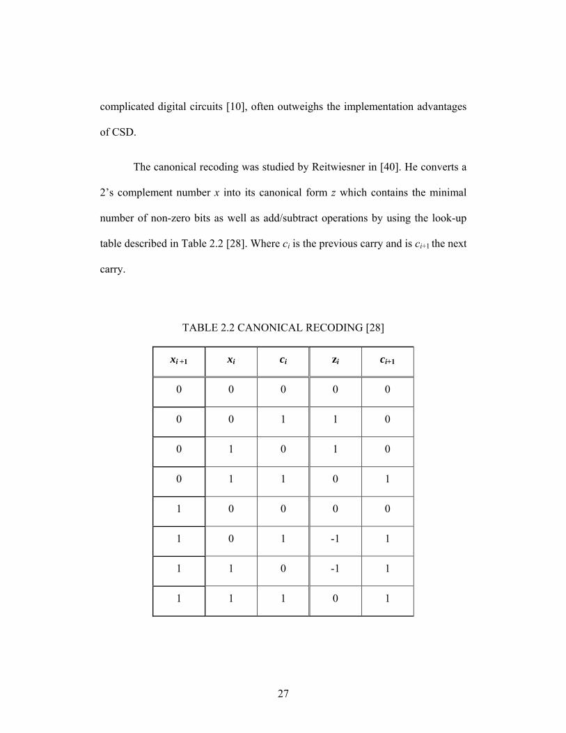
The canonical recoding was studied by Reitwiesner in [40]. He converts a
2’s complement number x into its canonical form z which contains the minimal
number of non-zero bits as well as add/subtract operations by using the look-up
table described in Table 2.2 [28]. Where ci is the previous carry and is ci+1 the next
carry.
TABLE 2.2 CANONICAL RECODING [28]
xi +1 xi ci zi ci+1
0 0 0 0 0
0 0 1 1 0
0 1 0 1 0
0 1 1 0 1
1 0 0 0 0
1 0 1 -1 1
1 1 0 -1 1
1 1 1 0 1
28
The main drawback to canonical recoding is that the bits of the multiplier
are generated sequentially along with carry bits, while Booth’s recoding is
carry-free and can be applied in parallel [28].
Also, in order to take full advantage of the minimal number of add/subtract
operations, the number of those operations must be variable which is difficult to
implement [28].
Ruiz and Manzano proposed a self-timed CSD multiplier based on the
canonical recoding algorithm in [10].
2.5.1.2 Minimal Signed Digit (MSD)
Another popular radix-two number representation is Minimal Signed Digit
Example: Assume c0=0
x=0111001 → z0=1, c1=0
x=011100 → z1=0, c2=0
x=01110 → z2=0, c3=0
x=0111 → z3= –1, c4=1
x=011 → z4= 0, c5=1
x=01 → z5=0, c6=1
x=(0)0 → z6=1, c7=0
z= 1001001
29
(MSD) [38] which includes all of the signed-digit representations having the same
number of non-zero digits as CSD. So, the MSD representation of a number is not
unique. In other words, CSD is just a special MSD number. For example, the
decimal number 105 can be expressed as:
10105 10101001 10011001CSD MSDx = = = . Although the CSD representation is
good for one constant, it is not the best for multiplication by multiple constants
because the CSD representation of a constant is unique and independent of the
other constants, leading to limited sub-expressions for multiple constants. Using
MSD representation, a given number can have multiple representations. By
properly exploiting the redundancy of MSD representations, the hardware
implementation can be significantly optimized by combining sub-expressions
occurring in coefficients. Consider the previous example, 10101001CSD requires 3
adders. However, 10011001 (8 1)(16 1)MSD = − − only needs 2 adders.
2.5.2 Constant multiplication problems
If the value of a multiplier is known a priori, the CSD expression can be
calculated offline, and it can be further improved by constant multiplication
techniques [41], such as Dempster-Macleod’s algorithm [15] or Bull-Horrocks’
algorithm [16].
30
Constant Multiplication (CM) problems include Single Constant
Multiplication (SCM) problems and Multiple Constant Multiplication (MCM)
problems. Usually, these problems are solved by using graph topology, so the
techniques developed to handle these problems are also called dependence-graph
algorithms [41].
2.5.2.1 Single Constant Multiplication methods (SCM)
Through the use of CSD representations, the number of adders and shifters
can be greatly reduced. However, further improvement is possible. Sometimes it is
more efficient to first factor the multiplier into several factors, then realize each
factor in a simple combination of powers-of-two, sums of two powers-of-two, or
differences of two powers-of-two. The problem of finding a multiplierless
multiplier block for the multiplication by a constant with the least number of
add/subtracts is known as the SCM problem, and it is NP-complete as shown in
[42]. An optimal solution for a constant less than or equal to 12 bits is called
Multiplier Adder Graph (MAG) which is designed by Dempster and Macleod in
[15]. Further improvement for constants up to 19 bits has been discussed in [43].
Using this idea, more adders can be saved. For example, consider a multiplier
93128a = . The 2’s complement representation is
31
1 3 4 5 793 0.1011101 2 2 2 2 2128
a − − − − −= = = + + + + (2.4)
which needs four adders. If we rewrite the multiplier a using CSD, we get
2 5 77
93 10100101 1 2 2 2128 2
a − − −= = = − − + . (2.5)
An implementation using this CSD representation requires three 2-input
adders and 3 shifts:
2 5 72 2 2ax x x x x− − −= − − + . (2.6)
We can rewrite a using MAG method as
93 31 3 (32 1) (4 1)128 32 4 32 4
a − −= = × = × (2.7)
to obtain
5 2(1 2 )(1 2 )ax x− −= − − (2.8)
which can be computed using 2 adders and 2 shifts.
Figure 2.6 shows these three types of implementations of multiplier
93128a =
visualized as graphs.
32
(a)
(b)
(c)
Figure 2.6 Multiplication by 93128 using (a) 2’s complement multiplier with 4
adds/subtractors; (b) CSD representation with 3 adds/subtractors (c) MAG method with 2 adds/subtractors.
X - -
2-5 2-2
aX
33
In hardware implementations, the shifts are typically implemented through
routing of signals rather than a clocked shifter circuit. This routing requirement
may or may not increase area needs [37].
2.5.2.2 Multiple constant multiplication methods
An extension of SCM is the problem of finding a multiplierless multiplier
block for the parallel multiplications by a set of N constants w0, w1..., wN with the
least number of add/subtracts. These problems are known as MCM problems [41].
Some well known algorithms to solve MCM problem that are frequently used in
FIR filters are Bull-Horrocks’ algorithm (BHA) [16] and its improved version
Bull-Horrocks Modified (BHM) [44]. These two algorithms simultaneously
multiply one input by N constants; thus, savings can be achieved by the overlapping
of intermediate results. Another MCM method which yields better results is RAG-n
[44]. It relies on the availability of an optimal single constant decomposition
lookup table and is limited to 19 bits. Since the sub-expressions are actually MAGs,
the MCM problem is also NP-complete.
Currently the best heuristic method for solving MCM problems that I know
is provided by Voronenko and Püschel in [41], which is called Hcub. Below I will
implement and compare this method with multiplier based design and CSD
34
encoded design. I will use an example loop filter that is a component in the
delta-sigma digital to analog (DA) converter to get better understanding of
multiplierless techniques.
2.5.3 Implementation of loop filter using multiplierless techniques
Delta-sigma (ΔΣ ) modulation has become the most popular method for
high-resolution A/D and D/A conversion [45]. Using feedback to shape the errors
results in a high-speed, low-resolution quantizer. Better SNR and linearity can be
achieved than with conventional converters [46]. The error-feedback ΔΣ
modulator topology is shown in Figure 2.7 [46]. Clever algorithms for the loop
filter must be combined with novel digital hardware to reduce space and increase
throughput. Multiplierless techniques become the method of choice to implement
the loop filter in this system [47].
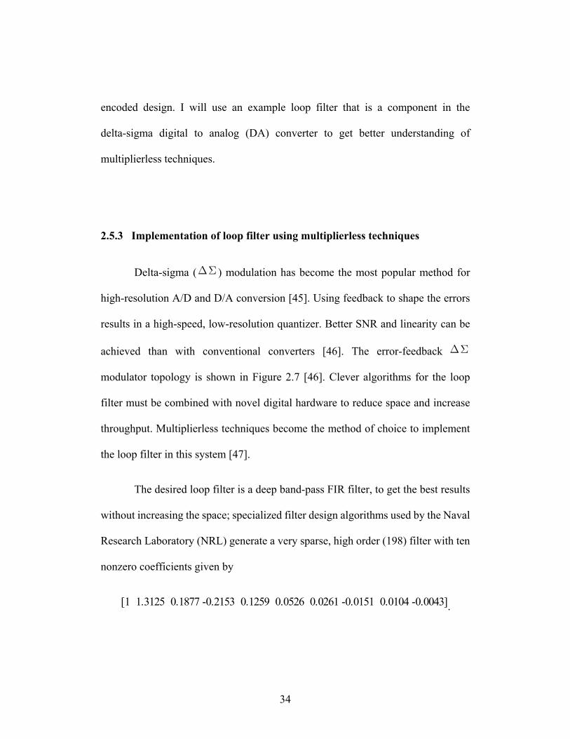
The desired loop filter is a deep band-pass FIR filter, to get the best results
without increasing the space; specialized filter design algorithms used by the Naval
Research Laboratory (NRL) generate a very sparse, high order (198) filter with ten
nonzero coefficients given by
[1 1.3125 0.1877 -0.2153 0.1259 0.0526 0.0261 -0.0151 0.0104 -0.0043].
35
Figure 2.7 Error-feedback ΔΣ architecture [46].
Multiplying these coefficients by 218 generates integer values which are easier to
manipulate for implementation:
[262144 344064 49215 -56441 33016 13787 6840 -3969 2726 -1120].
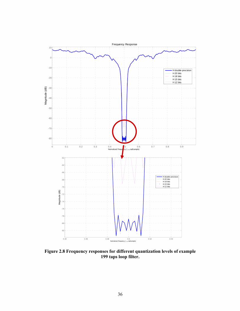
In Figure 2.8, I compare the frequency response results of the example loop
filter with different quantization levels. Also, I implement and analyze candidate
system architectures that balance speed, space and power, including multiplier
based design, CSD number system design, and MCM design. I chose transposed
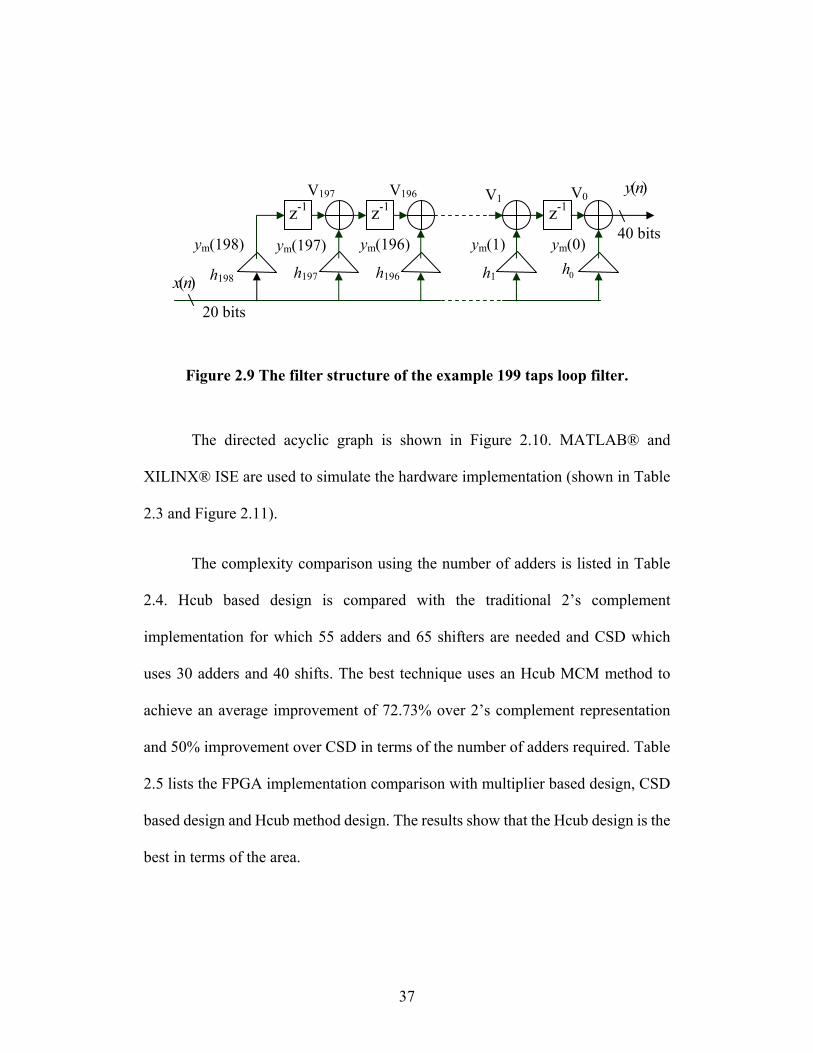
form as the basic filter structure (shown in Figure 2.9); 20 bits for each coefficient
hi (including sign bit) and each input sample x(n), internal computations ym use 40
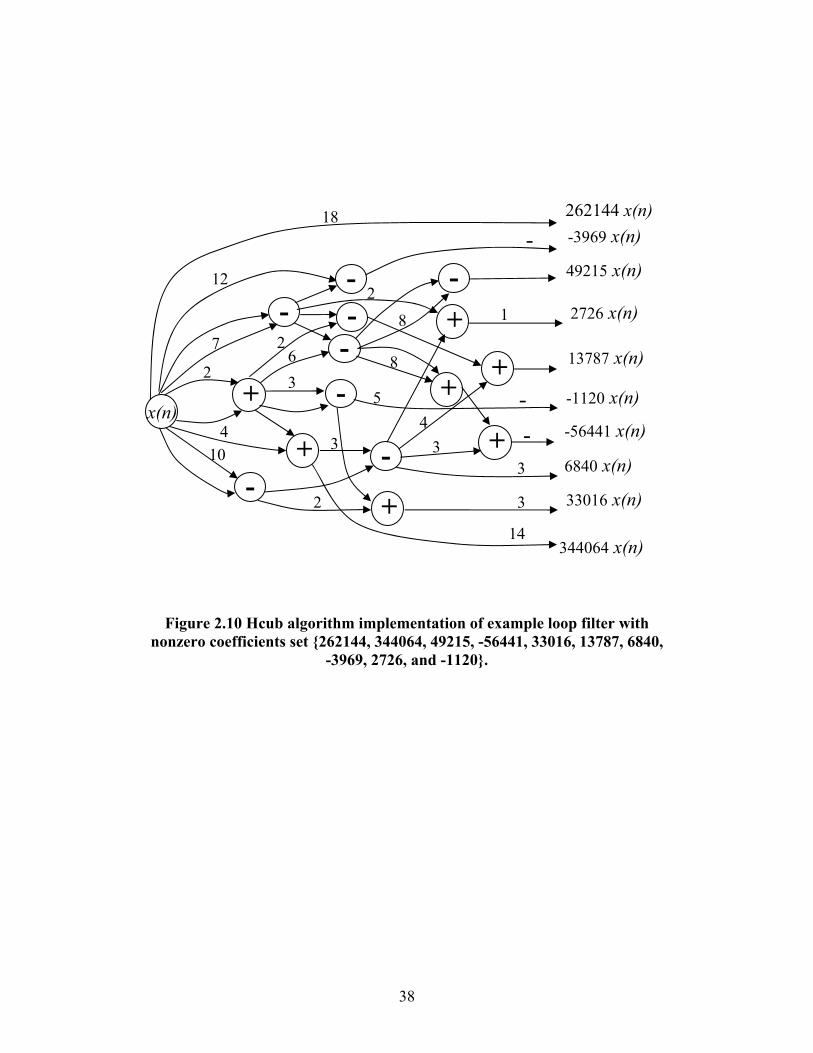
bits (no rounding). For MCM techniques, I use the Hcub method [41], a recent
algorithm that has the current best results to my knowledge. Also, I use the Hcub
generator [48] to create the directed acyclic graph (DAG) for the multiplierless
multiplier block that implements the parallel multiplications of the ten nonzero
coefficients in the loop filter.
+
+
Q
Loop filter
x(n) y(n)
e(n) + _
+
_
Quantizer
36
0 0.1 0.2 0.3 0.4 0.5 0.6 0.7 0.8 0.9
-80
-70
-60
-50
-40
-30
-20
-10
0
10
Normalized Frequency ( ×π rad/sample)
Mag
nitu
de (d
B)
Frequency Response
H double-precisionH 20 bitsH 18 bitsH 15 bitsH 12 bits
0.44 0.46 0.48 0.5 0.52 0.54
-82
-80
-78
-76
-74
-72
-70
-68
-66
-64
-62
Normalized Frequency ( ×π rad/sample)
Mag
nitu
de (d
B)
H double-precisionH 20 bitsH 18 bitsH 15 bitsH 12 bits
Figure 2.8 Frequency responses for different quantization levels of example 199 taps loop filter.
37
Figure 2.9 The filter structure of the example 199 taps loop filter.
The directed acyclic graph is shown in Figure 2.10. MATLAB® and
XILINX® ISE are used to simulate the hardware implementation (shown in Table
2.3 and Figure 2.11).
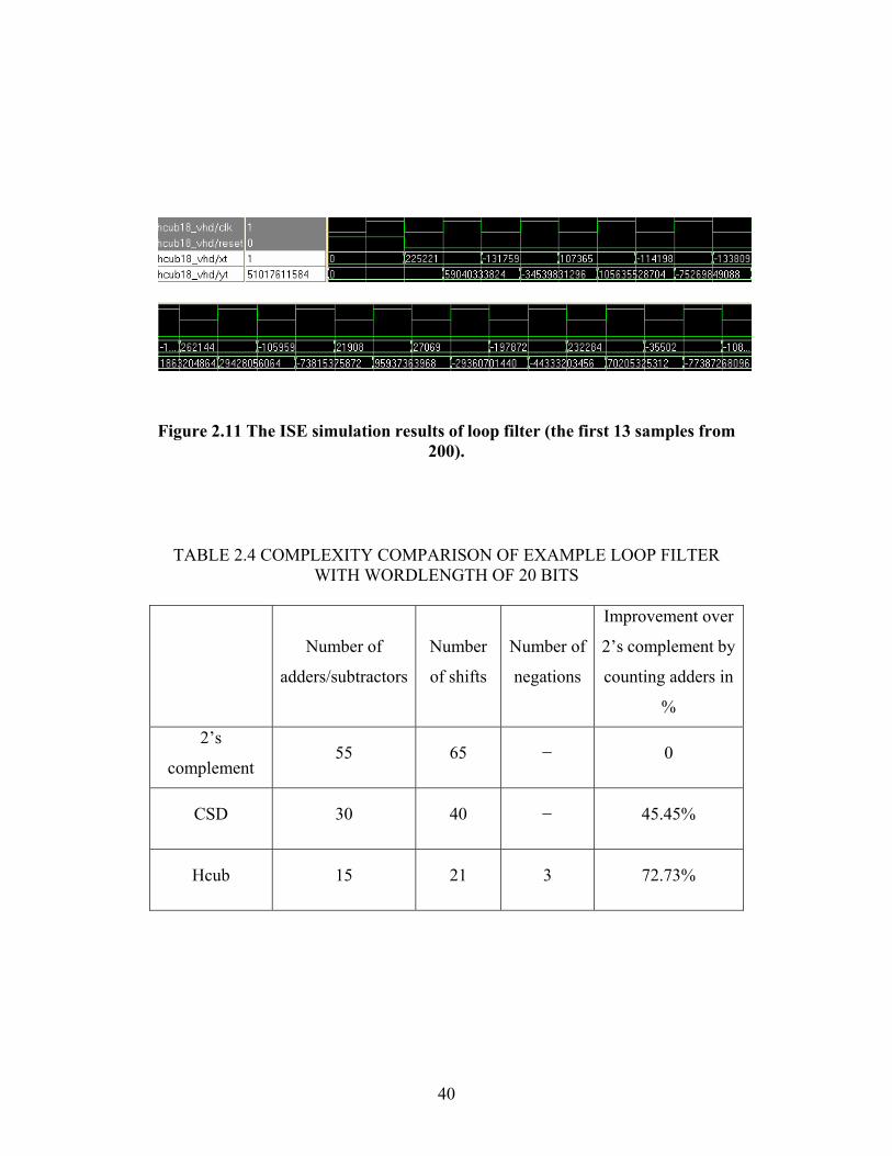
The complexity comparison using the number of adders is listed in Table
2.4. Hcub based design is compared with the traditional 2’s complement
implementation for which 55 adders and 65 shifters are needed and CSD which
uses 30 adders and 40 shifts. The best technique uses an Hcub MCM method to
achieve an average improvement of 72.73% over 2’s complement representation
and 50% improvement over CSD in terms of the number of adders required. Table
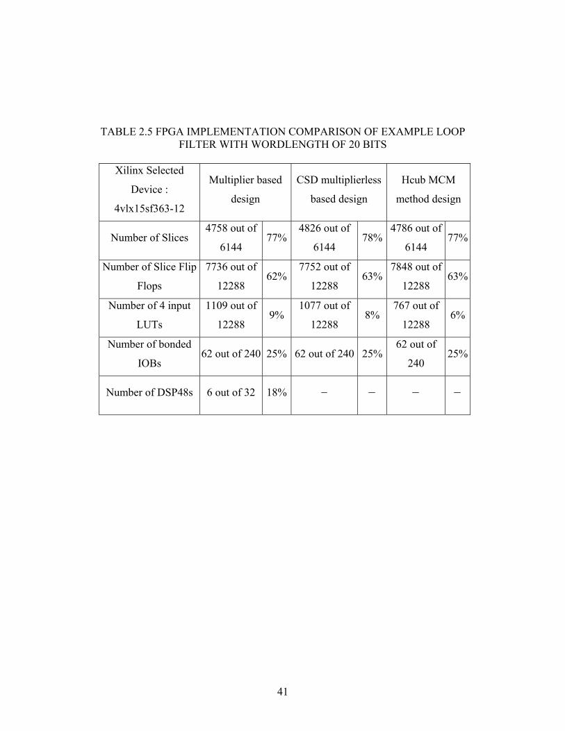
2.5 lists the FPGA implementation comparison with multiplier based design, CSD
based design and Hcub method design. The results show that the Hcub design is the
best in terms of the area.
z-1
( )x n
( )y n z-1 z-1
0h ym(198)
V197
h197 h196 h1
ym(197) ym(196) ym(0) ym(1)
V196 V1 V0
h198
20 bits
40 bits
38
Figure 2.10 Hcub algorithm implementation of example loop filter with nonzero coefficients set {262144, 344064, 49215, -56441, 33016, 13787, 6840,
-3969, 2726, and -1120}.
262144 x(n) -3969 x(n)
49215 x(n)
2726 x(n)
13787 x(n)
-1120 x(n)
-56441 x(n)
6840 x(n)
33016 x(n)
x(n) + -
2
7
-12 -
- 18
+ 4
3
-2 -6
-10
+
-3
2
+-
8 2
1
+
+
4
+8
3 3
3
5 - -
344064 x(n) 14
39
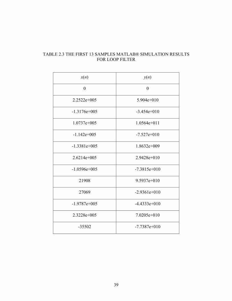
TABLE 2.3 THE FIRST 13 SAMPLES MATLAB® SIMULATION RESULTS FOR LOOP FILTER
x(n) y(n)
0 0
2.2522e+005 5.904e+010
-1.3176e+005 -3.454e+010
1.0737e+005 1.0564e+011
-1.142e+005 -7.527e+010
-1.3381e+005 1.8632e+009
2.6214e+005 2.9428e+010
-1.0596e+005 -7.3815e+010
21908 9.5937e+010
27069 -2.9361e+010
-1.9787e+005 -4.4333e+010
2.3228e+005 7.0205e+010
-35502 -7.7387e+010
40
Figure 2.11 The ISE simulation results of loop filter (the first 13 samples from 200).
TABLE 2.4 COMPLEXITY COMPARISON OF EXAMPLE LOOP FILTER
WITH WORDLENGTH OF 20 BITS
Number of
adders/subtractors
Number
of shifts
Number of
negations
Improvement over
2’s complement by
counting adders in
%
2’s
complement 55 65 0
CSD 30 40 45.45%
Hcub 15 21 3 72.73%
41
TABLE 2.5 FPGA IMPLEMENTATION COMPARISON OF EXAMPLE LOOP FILTER WITH WORDLENGTH OF 20 BITS
Xilinx Selected
Device :
4vlx15sf363-12
Multiplier based
design
CSD multiplierless
based design
Hcub MCM
method design
Number of Slices 4758 out of
6144 77%
4826 out of
6144 78%
4786 out of
6144 77%
Number of Slice Flip
Flops
7736 out of
12288 62%
7752 out of
12288 63%
7848 out of
12288 63%
Number of 4 input
LUTs
1109 out of
12288 9%
1077 out of
12288 8%
767 out of
12288 6%
Number of bonded
IOBs 62 out of 240 25% 62 out of 240 25%
62 out of
240 25%
Number of DSP48s 6 out of 32 18%
42
Chapter 3
A NOVEL MULTIPLIERLESS HARDWARE
IMPLEMENTATION METHOD FOR ADAPTIVE
FILTER COEFFICIENTS
3.1 Introduction
“Implementation is everything” in the construction of practical adaptive
filters [49]. These practical hardware implementations typically require high
throughput, low power consumption and small area. For fixed coefficient filters,
multiplierless implementation approaches are used. However, since the coefficients
of an adaptive filter are not fixed, general multipliers are needed. Multipliers are
expensive in terms of chip area, power consumption, and operation time. For
practical high performance adaptive filters, this limitation must be overcome.
Multipliers are often implemented in hardware using shift-and-add
techniques. The number of add operations depends on the number of 1’s in the
binary multiplier. The number of add/shift operations is directly related to the
power consumption and area required. Array techniques are used to achieve high
43
throughput, at the cost of significant increases in power and area.
One effective method to reduce the number of shift/add operations in
multiplier hardware is to reduce the wordlength of the multipliers (e.g. filter
coefficients). However, reducing the wordlength can significantly degrade the
performance of the implemented algorithm.
When the value of the multiplier is known, multiplication can be
implemented using alternate number representations for the multiplier, such as the
CSD [39] or SPT representation [8]. CSD representation has proven to be useful for
implementing multipliers with less complexity, because the cost of multiplication
is a direct function of the number of nonzero bits in the multiplier. It is shown in [9]
that for a n-bit 2’s complement multiplier the number of add/subtract operations
never exceeds n/2 and can be reduced to n/3 on average, as the wordlength of
multiplier grows.
Many researchers have addressed the question of how to convert 2’s
complement to CSD numbers. Some of these approaches are from the point of view
of reducing computational complexity [50], [51], but are not suitable for
implementation into hardware. Other approaches try to improve the
implementation efficiency by limiting the area and power consumption [10], [11].
However, some introduce errors, and others are still complex.
44
If the multiplier is known a priori, as is the case for most FIR and IIR filter
implementations, the CSD expression can be calculated offline and the
implementation can be further improved via computational techniques such as
Dempster-Macleod’s algorithm [15]. Using this technique, more adders can be
saved. However, when the multiplier is unknown or can change over time, as is the
case for adaptive filters, these techniques are not applicable. To benefit from the
CSD implementation advantages, the conversion of numbers from 2’s complement
to CSD format must be implemented in hardware. Unfortunately, the cost of
conversion using methods such as those based on Look-Up-Table (LUT) [29] or
canonical recoding techniques [40] often outweighs the implementation advantages
of CSD.
In this chapter, I introduce a new hardware implementation method to
convert 2’s complement numbers to CSD numbers; we call it FastCSD [18]. My
method has several advantages. First, unlike LUT methods, my technique does not
require a fixed word length to be known a priori. In addition, the proposed method
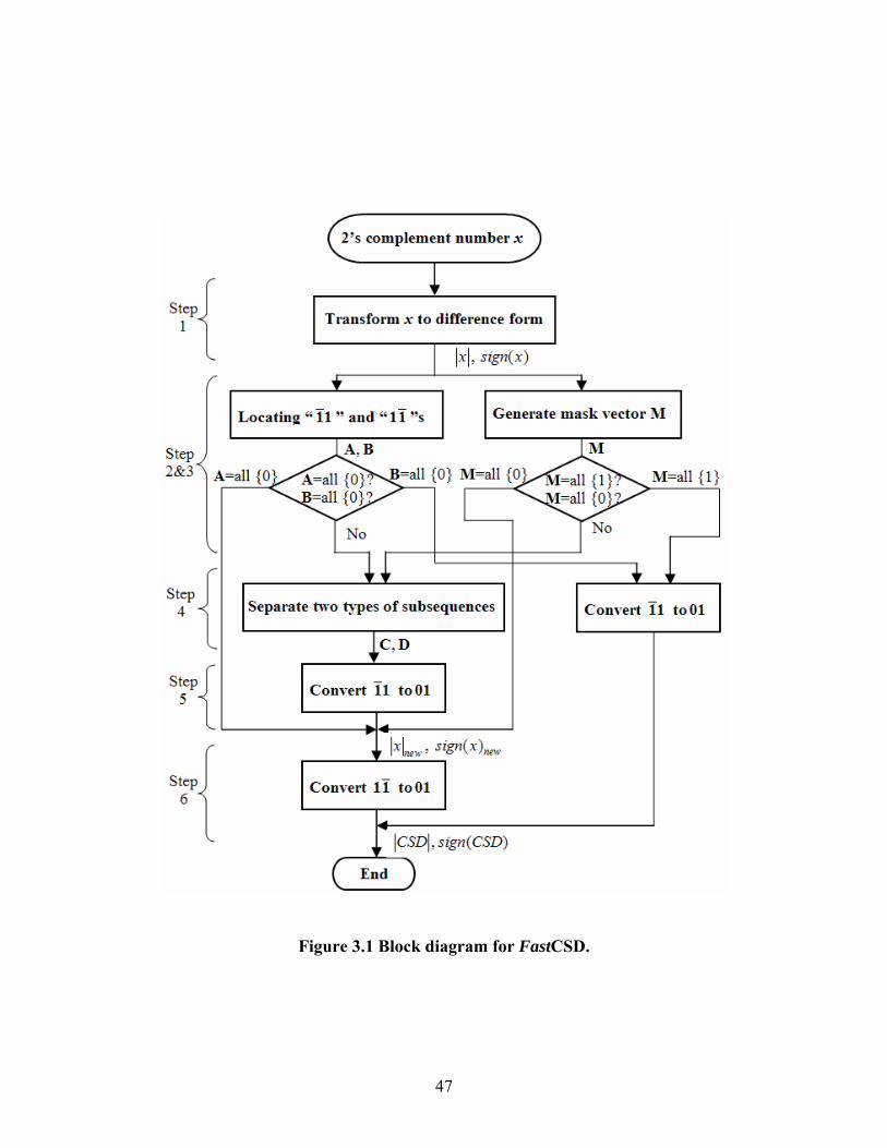
uses a limited number of shift and logic operations, instead of the overlap and
scanning used for methods like Booth’s recoding [12] and canonical recording.
This allows the number of computational cycles to be fixed and independent of the
wordlength of the multiplier, k . So, the time required is constant. Furthermore,
because all the CSD bits are produced simultaneously, the conversion speed, and
45
thus the throughput, is improved.
FastCSD can be applied to efficiently implement digital filters with
non-fixed coefficients, such as adaptive filters. The implementation can be further
improved through the use of parallel processing with a reasonable sacrifice in the
area consumption using FPGAs.
3.2 New 2’s complement to CSD conversion method (FastCSD)
The new method to convert a 2’s complement number to CSD
representation is a simple series of shift and logic operations, which are
implemented in six processing steps as shown in Figure 3.1 and described in the
following paragraphs.
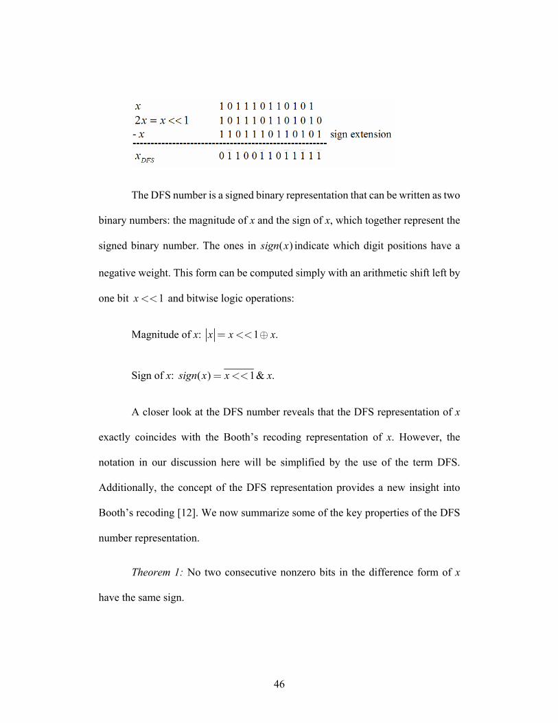
Step 1: Transform x to difference form: x = 2x - x . To reduce the many
additions arising from a string of ones, we use the simple concept that 2x x x= − to
convert x to another form we refer to as the difference form signed (DFS) number
[19], [20]. In the DFS representation, a number may contain instances of the digit
pairs “ 11” and “1 1 ,” but sequences of two consecutive ones or two consecutive
negative one digits cannot occur. DFS conversion is illustrated in the following
example:
46
The DFS number is a signed binary representation that can be written as two
binary numbers: the magnitude of x and the sign of x, which together represent the
signed binary number. The ones in ( )sign x indicate which digit positions have a
negative weight. This form can be computed simply with an arithmetic shift left by
one bit 1x << and bitwise logic operations:
Magnitude of x: 1 .x x x= << ⊕
Sign of x: ( ) 1& .sign x x x= <<
A closer look at the DFS number reveals that the DFS representation of x
exactly coincides with the Booth’s recoding representation of x. However, the
notation in our discussion here will be simplified by the use of the term DFS.
Additionally, the concept of the DFS representation provides a new insight into
Booth’s recoding [12]. We now summarize some of the key properties of the DFS
number representation.
Theorem 1: No two consecutive nonzero bits in the difference form of x
have the same sign.
47
Figure 3.1 Block diagram for FastCSD.
48
Proof: If two consecutive nonzero bits in the difference form of x have the
same sign, i.e. “11” or “ 11 ”, then the corresponding positions of 2x and x should
be either “11” and “ 00 ” or “ 00 ” and “11”. However since 2 1x x= << , then the
(i+1)th bit of 2x must be the same as the ith bit of x which cannot be the case. Hence,
the difference form cannot contain a sequence “11” or “ 11 ”. ■
Theorem 2: To convert a 2’s complement number x to the CSD
representation, we only need to replace occurrences of the bit pair “ 11” with “ 01 ”
and/or the bit pair “1 1 ” with “ 01 ” in the difference form of x starting from the
least significant bit (LSB).
Proof: Let DFSx be a DFS number and let M ∈ be the number of
sequences of two or more consecutive nonzero digits that occur in DFSx , where
0.M ≥ If 0,M = then DFSx is already a valid CSD representation. Therefore, it is
sufficient to consider only cases where 1.M ≥ Let 1 2, , , MΓ Γ Γ… denote the
sequences of two or more consecutive nonzero digits that occur in DFSx in order of
decreasing length (so that 1Γ is the longest such sequence) and let mk denote the
length in digits of the sequence .mΓ It follows immediately from Theorem 1 that
mΓ is an alternating sequence of mk occurrences of the digits “1” and “ 1 ”, where
2.mk ≥ If the low-order digit pair of mΓ is “1 1 ”, then it may be replaced by the
49
equivalent digit pair “01”; alternatively, if the low order digit pair is “ 11”, then it
may be replaced by the equivalent pair “0 1 ”. This replacement converts mΓ from
a sequence of mk consecutive nonzero digits to a sequence of 2mk − consecutive
nonzero digits and may be repeated until the length of mΓ is reduced to zero. The
desired result follows immediately by repeating this argument for all .m M≤ ■
Step 2: Locating “ 11 ” and “ 11 ”s. To locate the positions of the “ 11”
and “1 1 ” strings, I find the digits that are ‘ 1 ’ from the ‘1’s in ( )sign x , then use
“shift/and” operation to get two vectors A and B.
A= 1& ( )x sign x<<
where each ‘1’ in A corresponds to a string “ 11”.
B= 1& ( )x sign x>>
where each ‘1’ in B corresponds to a string “11 ”.
Note that 1x >> denotes a logical right shift by one bit.
Theorem 3: Each ‘1’ in A denotes the position of a “ 11” string in the
difference form, and each ‘1’ in B corresponds to a string “11 ” in the difference
form.
50
Proof:
1 11 11 & ( ) 10if 11 { , after 1 ,
010( ) 10
11 1 11if 11 { , after 1 ( ) 01 & ( ) 01 ,
0
0if 0 {
i
xx sign x sx x
sign x
x xx xsign x sign x
xx
s
A
A
<< ×=
= ⇔ << ⇒=
= << ×= ⇔ << ⇒= ×
× ×
== ⇔ 1 0, after 1
( ) 0 & ( ) 0 , 00
xxign x sign x
A
<< ×<< ⇒= ×
where × indicates don’t care (can be either ‘1’ or ‘0’), and is can not be ‘1’, based
on Theorem 1. Since if '1'is = and 1 '1'is + = , that means the difference form of x
has a consecutive “ 11 ” in the corresponding position, which is impossible. Thus,
each ‘1’ in A stands for a pair of “ 11”. ■
Similarly,
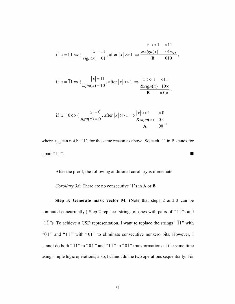
51
2
1 11 11 & ( ) 01if 11 { , after 1 ,
010( ) 01
11 1 11if 11 { , after 1 ( ) 10 & ( ) 10 ,
0
0if 0 {
i
xx sign x sx x
sign x
x xx xsign x sign x
xx
sig
B
B
+
>> ×=
= ⇔ >> ⇒=
= >> ×= ⇔ >> ⇒= ×
× ×
== ⇔ 1 0, after 1
( ) 0 & ( ) 0 , 00
xxn x sign x
A
>> ×>> ⇒= ×
where 2is + can not be ‘1’, for the same reason as above. So each ‘1’ in B stands for
a pair “11 ”. ■
After the proof, the following additional corollary is immediate:
Corollary 3A: There are no consecutive ‘1’s in A or B.
Step 3: Generate mask vector M. (Note that steps 2 and 3 can be
computed concurrently.) Step 2 replaces strings of ones with pairs of “ 11”s and
“11 ”s. To achieve a CSD representation, I want to replace the strings “ 11” with
“ 01 ” and “11 ” with “ 01 ” to eliminate consecutive nonzero bits. However, I
cannot do both “ 11” to “01 ” and “11 ” to “01” transformations at the same time
using simple logic operations; also, I cannot do the two operations sequentially. For
52
example, if “111 ” and “ 111 ” exist in the same sequence, no matter which
replacement I do first the result has consecutive nonzero bits, such as “011” or
“ 011 ”.
So an alternative approach is needed. This leads to Theorem 4 as follows:
Theorem 4: The zero bits in the difference form of x correspond to zero
digits in the CSD form.
Proof: It follows from Theorem 2 that, to convert the DFS representation of
x to CSD, it is required only to replace occurrences “ 11 ” with “ 01 ” and
occurrences “11 ” with “ 01 ”. These replacements will never generate a carry.
Moreover, the resulting two-bit segments will never propagate a carry. Therefore,
zero bits in DFS representation will always remain unchanged in the CSD
representation. ■
Based on Theorem 4, it can be observed that the zeros in the difference form
of x separate the sequence into several parts. We want to transform “ 11” to “ 01 ”
and “11 ” to “01” separately beginning with the nonzero bit adjacent to the ‘0’
(working from right to left). We form a mask vector M to separate the
subsequences. M has the same length as x, whenever the subsequence begins with
‘1’, the corresponding subsequence in M is all ones, otherwise it is all zeros. For
53
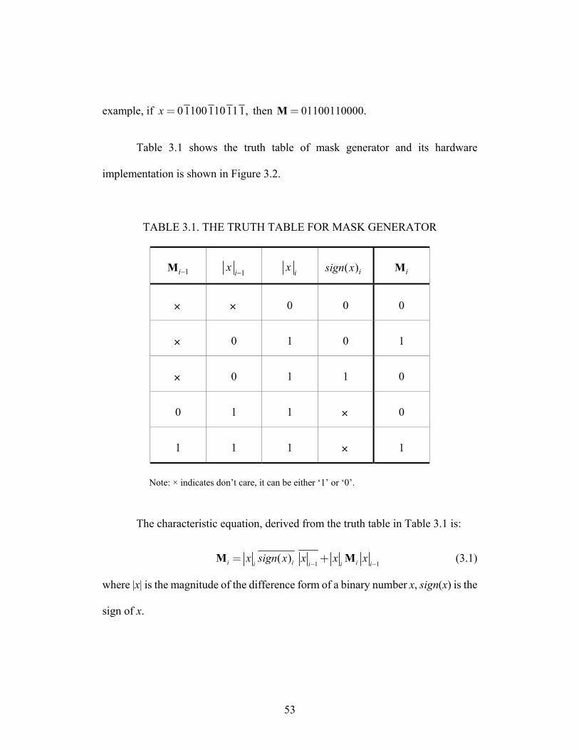
example, if 01100110111,x = then 01100110000.=M
Table 3.1 shows the truth table of mask generator and its hardware
implementation is shown in Figure 3.2.
TABLE 3.1. THE TRUTH TABLE FOR MASK GENERATOR
1iM − 1ix − ix ( )isign x iM
× × 0 0 0
× 0 1 0 1
× 0 1 1 0
0 1 1 × 0
1 1 1 × 1
Note: × indicates don’t care, it can be either ‘1’ or ‘0’.
The characteristic equation, derived from the truth table in Table 3.1 is:
1 1( ) i i ii i i i
x sign x x x x− −
= +M M (3.1)
where |x| is the magnitude of the difference form of a binary number x, sign(x) is the
sign of x.
54
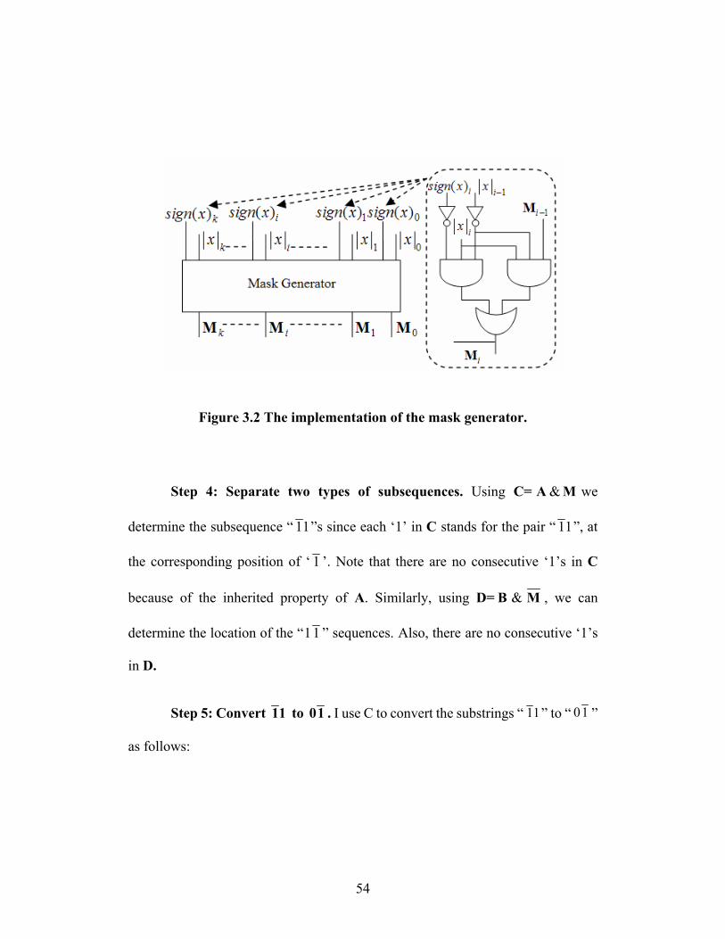
Figure 3.2 The implementation of the mask generator.
Step 4: Separate two types of subsequences. Using C= &A M we
determine the subsequence “ 11”s since each ‘1’ in C stands for the pair “ 11”, at
the corresponding position of ‘ 1 ’. Note that there are no consecutive ‘1’s in C
because of the inherited property of A. Similarly, using D= & B M , we can
determine the location of the “11 ” sequences. Also, there are no consecutive ‘1’s
in D.
Step 5: Convert 11 to 01 . I use C to convert the substrings “ 11” to “ 01 ”
as follows:
55
( ) ( ) ( 1)
new
new
x x
sign x sign x
C
C | C >>
= ⊕
= ⊕ .
(3.2)
The following display illustrates the technique schematically.
new i-1
11 ( ) 10 01 11 10 11 01 00 10( ) 10 ( ) 01 01 | ( 1) 110
( )
new
new
new
ne
x sign xxx xx
sign x sign x x csign x
C
C
C C
⎧ =⎧⎪ == ⊕⎪ ⎪
⇔ = ⇒ ⇒⎨ ⎨ ⊕=⎪ ⎪ =⎩⎪ >>=⎩ 01w
where 1ic − can not be ‘1’, based on Theorem 1.
Step 6: Convert 11 to 01 . Similar to Step 5, I convert “1 1 ” to “ 01 ” using
D as follows:
( ) ( )
( 1)
new
new
sign CSD sign x
CSD x
D
D
= ⊕
= << ⊕ .
(3.3)
Example: Figure 3.3 shows the conversion of x=101110110101 to CSD.
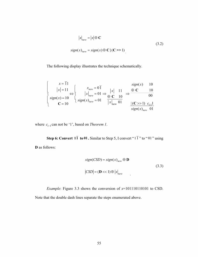
Note that the double dash lines separate the steps enumerated above.
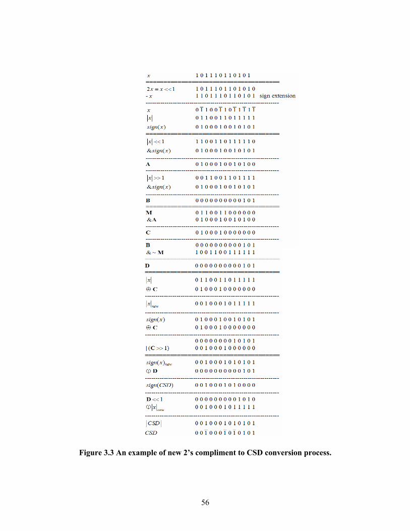
56
Figure 3.3 An example of new 2’s compliment to CSD conversion process.
57
3.3 Comparison with Booth’s recoding and LUT techniques
The radix-4 modified Booth’s recoding algorithm has been widely used in
modern high-speed multiplication circuits [27]. Using a modified Booth algorithm,
adjacent 3-bit segments of 2’s complement numbers are converted into the digit
set { }2, 1, 0± ± . Although modified Booth’s recoding reduces a k-bit 2’s
complement multiplier to 2k⎡ ⎤⎢ ⎥ digits, it is based on overlapped multiple-bit
scanning schemes. So, no matter how large the radix is, the number of scan cycles
is a function of the multiplier word length k. As k increases, the number of scan
cycles increases as well. Booth’s recoding can be used for parallel multipliers if
duplicated recoding logic and multiple selection circuits are used, however, that
requires huge area consumption.
FastCSD is a fully parallel process; it reduces the number of add/subtract
operations to the minimum. Unlike the modified Booth’s recoding algorithm, the
number of operations of FastCSD is fixed as well as the total delay time. So, the
time is constant regardless of the word length k. The detailed performance analysis
is given in Table 3.2. Compared with the modified Booth’s recoding algorithm
whose operation time is a function of multiplier word length k, FastCSD requires a
delay of only 4 shifts and 8 logic gates for the worst case. Furthermore, the
throughput can be further improved by incorporating parallel processing. My
method is attractive in terms of both throughput and computational complexity.
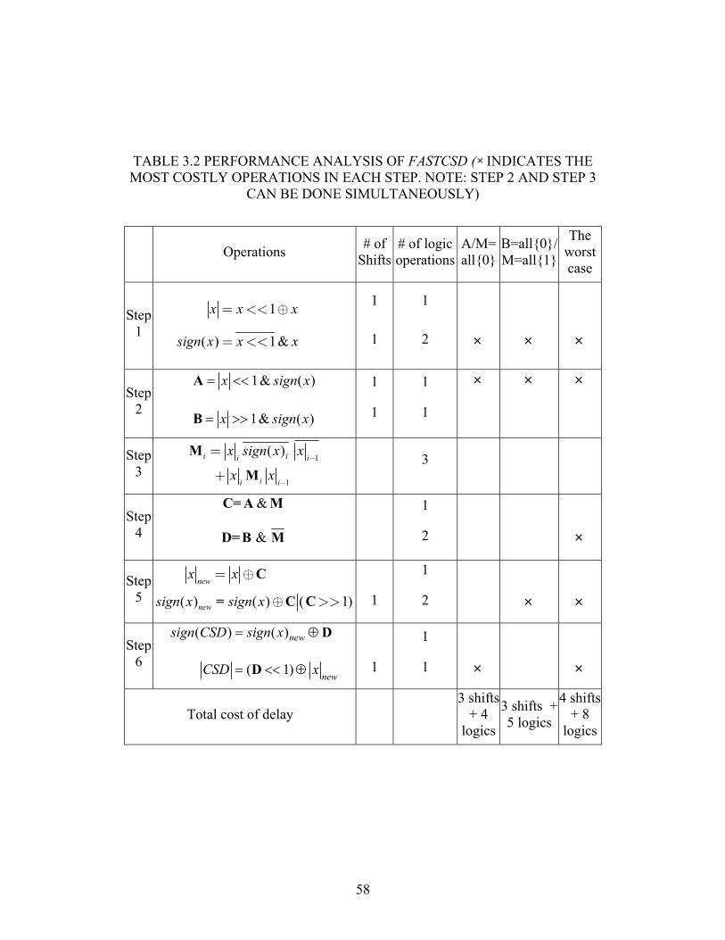
58
TABLE 3.2 PERFORMANCE ANALYSIS OF FASTCSD ( × INDICATES THE MOST COSTLY OPERATIONS IN EACH STEP. NOTE: STEP 2 AND STEP 3
CAN BE DONE SIMULTANEOUSLY)
Operations # of Shifts
# of logic operations
A/M= all{0}
B=all{0}/ M=all{1}
The worst case
Step 1
1
( ) 1&
x x x
sign x x x
= << ⊕
= <<
1
1
1
2
×
×
×
Step 2
1& ( )
1& ( )
x sign x
x sign x
A
B
= <<
= >>
1
1
1
1
× × ×
Step 3
1
1
( ) i ii i
ii i
x sign x x
x x−
−
=
+
M
M 3
Step 4
C= &A M
D= & B M
1
2
×
Step 5 ( ) ( ) ( 1)
new
new
x x
sign x sign x
= ⊕
⊕ >>
C
= C C
1
1
2
×
×
Step 6
( ) ( )
( 1)
new
new
sign CSD sign x
CSD x
D
D
= ⊕
= << ⊕
1
1
1
×
×
Total cost of delay 3 shifts
+ 4 logics
3 shifts + 5 logics
4 shifts + 8
logics
59
Another commonly used technique for FPGA-based hardware is
Look-Up-Table (LUT) [29], [52]. Many algorithms used in DSP, such as filters, are
based on constant coefficient values. So, a Look-Up-Table can be used to
implement the multiplier by storing pre-computed partial products of the fixed
coefficient in distributed ROM to reduce the logic content. An advantage of this
approach is that the delay is just a memory access; so it is fast. However, a
disadvantage is that the table size grows exponentially with the input, so it is
space-intensive. So, a LUT approach requires the multiplier’s word length to be
fixed and the value of multiplier to be known prior to implementation.
The proposed method does not have the disadvantages of the LUT
implementation. It does not require a fixed multiplier word length, nor is it required
for the multiplier value to be known a priori. Thus, my method can be applied to
efficiently implement digital filters with non-fixed coefficients, such as adaptive
filters. In addition, my method is simple, requiring only several shifts and logic
operations. Since my method produces all of the CSD digits simultaneously, the
conversion speed, and thus the throughput, is improved.
60
Chapter 4
A MULTIPLIER STRUCTURE BASED ON A NOVEL
REAL-TIME CSD RECODING
4.1 Introduction
Adaptive filters have achieved widespread acceptance and are included in
many digital signal processing application areas such as communications and
signal preconditioning [3]. The coefficients of an adaptive filter change with time,
based on the adaptation (learning) algorithm. Many researchers have addressed the
question of how to implement the multiplications for fixed-coefficient filters, but
these techniques are not applicable to adaptive filters and other inner-product
computations in which the multipliers are not know a priori. Recently there has
been a renewed interest in adaptable-coefficient filters [3], [6], [8], [13], [17]. My
previous work with adaptive filter implementations has focused on the
development of an efficient multiplier [21], [53].
In general, there is a tradeoff between the hardware complexity and the
filter performance associated with the wordlength of the multipliers (usually
61
coefficients). Increased coefficient wordlength increases implementation
complexity, and decreased coefficient wordlength results in greater filter response
error. This tradeoff is fundamental to the implementation of all filters.
In fixed coefficient filters, multiplierless techniques are typically
implemented by encoding the coefficients in CSD [39] or SPT representations [8].
If the multiplier is known a priori, the CSD expression can be calculated offline
and it can be further improved by Dempster-Macleod’s algorithm [15] or similar
techniques [16], [41], [44], which can save additional adders. However, when the
multiplier is unknown or non-fixed, these techniques cannot be applied. In this case,
the conversion of numbers from 2’s complement to CSD format can be
implemented in hardware to simplify the multiplications. The conversion can be
implemented with look-up tables [29] or canonical recoding techniques [40], but
these all are costly in terms of the additional implementation overhead.
In this chapter, I introduce a new iterative multiplier structure which is
based on a novel real-time CSD recoding [19], [20]. Since this structure does not
require a fixed value for the multiplier input to be known a priori, it has broad
applications. The real-time CSD recoding multiplier has several advantages. First,
since it converts 2’s complement numbers to CSD numbers in real time, it requires
less shift/add/subtract operations compared to traditional modified (radix-4) Booth
recoding. As a result, the power consumption and area requirements in the
62
hardware implementation of DSP algorithms can be greatly reduced. In addition,
unlike modified Booth’s recoding [12], only three possible multiples of
multiplicand a (-a, 0, a) are used. So, the overhead for the multiple generation part
of the structure can be reduced. Furthermore, the proposed multiplier can be
applied to efficiently implement digital filters with non-fixed coefficients, such as
adaptive filters [3]. The implementation efficiency can be further improved by
properly incorporating parallel processing with a reasonable sacrifice in the area
consumption of FPGAs.
4.2 Real-time CSD Multiplier Structure
Instead of converting a binary number into its CSD representation, in the
proposed design, the CSD recoder only generates corresponding control signals.
Controlled by these signals, the multiplier actually operates based on the CSD logic.
For better understanding of my method, in this section, I use the Difference Form
Signed (DFS) number system introduced in Chapter 3, which has two main
properties:
Property 1: No two consecutive nonzero bits in the difference form of x
have the same sign.
Property 2: To convert a 2’s complement number x to the CSD
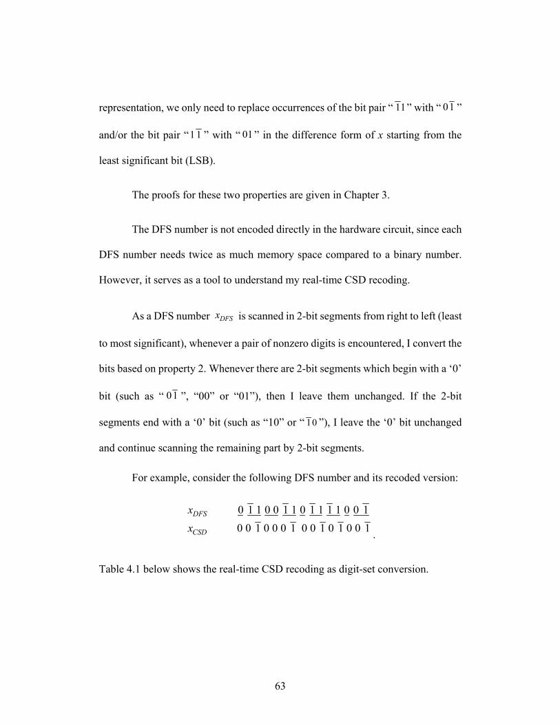
63
representation, we only need to replace occurrences of the bit pair “ 11” with “ 01 ”
and/or the bit pair “1 1 ” with “ 01 ” in the difference form of x starting from the
least significant bit (LSB).
The proofs for these two properties are given in Chapter 3.
The DFS number is not encoded directly in the hardware circuit, since each
DFS number needs twice as much memory space compared to a binary number.
However, it serves as a tool to understand my real-time CSD recoding.
As a DFS number DFSx is scanned in 2-bit segments from right to left (least
to most significant), whenever a pair of nonzero digits is encountered, I convert the
bits based on property 2. Whenever there are 2-bit segments which begin with a ‘0’
bit (such as “ 01 ”, “00” or “01”), then I leave them unchanged. If the 2-bit
segments end with a ‘0’ bit (such as “10” or “ 10 ”), I leave the ‘0’ bit unchanged
and continue scanning the remaining part by 2-bit segments.
For example, consider the following DFS number and its recoded version:
0 1 1 0 0 1 1 0 1 1 1 1 0 0 1 0 0 1 0 0 0 1 0 0 1 0 1 0 0 1
DFS
CSD
xx .
Table 4.1 below shows the real-time CSD recoding as digit-set conversion.
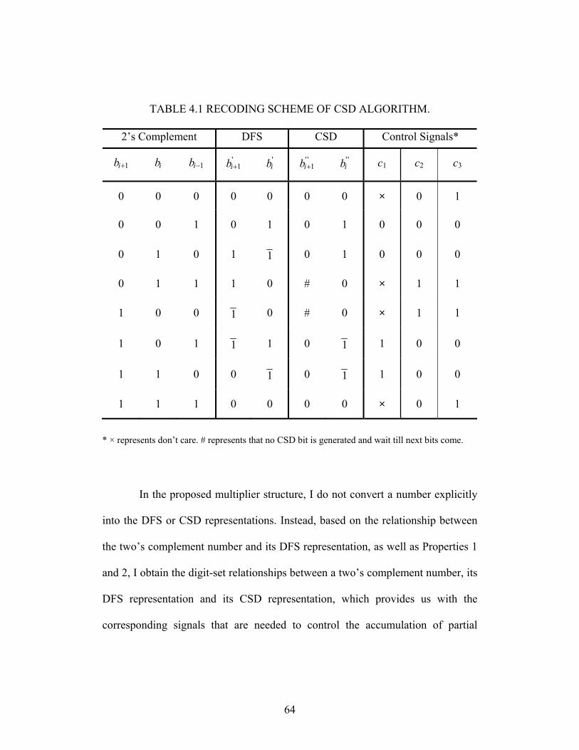
64
TABLE 4.1 RECODING SCHEME OF CSD ALGORITHM.
2’s Complement DFS CSD Control Signals*
1ib + ib 1ib − '1ib + '
ib ' '1ib + ' '
ib c1 c2 c3
0 0 0 0 0 0 0 × 0 1
0 0 1 0 1 0 1 0 0 0
0 1 0 1 1 0 1 0 0 0
0 1 1 1 0 # 0 × 1 1
1 0 0 1 0 # 0 × 1 1
1 0 1 1 1 0 1 1 0 0
1 1 0 0 1 0 1 1 0 0
1 1 1 0 0 0 0 × 0 1
* × represents don’t care. # represents that no CSD bit is generated and wait till next bits come.
In the proposed multiplier structure, I do not convert a number explicitly
into the DFS or CSD representations. Instead, based on the relationship between
the two’s complement number and its DFS representation, as well as Properties 1
and 2, I obtain the digit-set relationships between a two’s complement number, its
DFS representation and its CSD representation, which provides us with the
corresponding signals that are needed to control the accumulation of partial
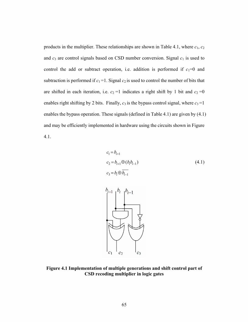
65
products in the multiplier. These relationships are shown in Table 4.1, where c1, c2
and c3 are control signals based on CSD number conversion. Signal c1 is used to
control the add or subtract operation, i.e. addition is performed if c1=0 and
subtraction is performed if c1 =1. Signal c2 is used to control the number of bits that
are shifted in each iteration, i.e. c2 =1 indicates a right shift by 1 bit and c2 =0
enables right shifting by 2 bits. Finally, c3 is the bypass control signal, where c3 =1
enables the bypass operation. These signals (defined in Table 4.1) are given by (4.1)
and may be efficiently implemented in hardware using the circuits shown in Figure
4.1.
1 1
2 1 1
3 1
( )
i
i i i
i i
c b
c b b b
c b b
+
+ −
−
=
= ⊕
= ⊕
(4.1)
Figure 4.1 Implementation of multiple generations and shift control part of CSD recoding multiplier in logic gates
66
The block diagram of the proposed iterative multiplier structure based on
this novel CSD encoding is given in Figure 4.2. The corresponding signal flow
chart is provided in Figure 4.3. From the flow chart, it is clear that this encoder
generates directly in hardware the control signals required to realize a multiplier
based on the CSD representation.
From Figures 4.2 and 4.3, it can be seen that the number of iterations
required by the real-time CSD recoding multiplier is data dependent and uses
shifting by a variable number of bits. Usually, shifting by a variable number of bits
means that a register-based shifter is needed, which adds to the time and energy
consumption for each iteration; in contrast, shifting by a constant number of bits
can be conveniently implemented by direct wire connections and requires very low
cost of in terms of energy and chip area.
However, the design proposing here does not in fact require arbitrary shifts,
but only shifts by one or by two bits. Thus, the design can be implemented simply
with a pair of hardwired shifts, where shifting by one bit or by two is selected by the
control signal c2. This implementation enables us to achieve the advantages of
variable shifting at the cost of constant shifting. Note that the computation speed of
the proposed multiplier structure can be further improved through the use of
advanced adders and asynchronous circuit techniques.
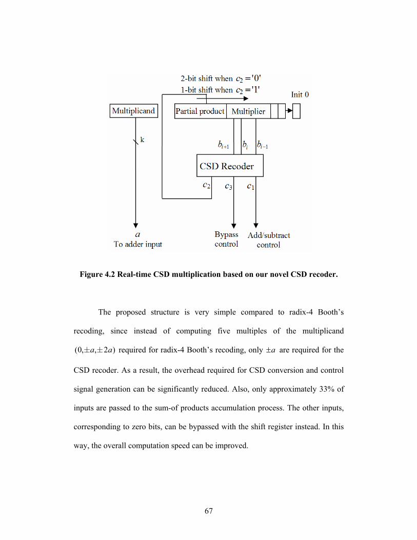
67
Figure 4.2 Real-time CSD multiplication based on our novel CSD recoder.
The proposed structure is very simple compared to radix-4 Booth’s
recoding, since instead of computing five multiples of the multiplicand
(0, , 2 )a a± ± required for radix-4 Booth’s recoding, only a± are required for the
CSD recoder. As a result, the overhead required for CSD conversion and control
signal generation can be significantly reduced. Also, only approximately 33% of
inputs are passed to the sum-of products accumulation process. The other inputs,
corresponding to zero bits, can be bypassed with the shift register instead. In this
way, the overall computation speed can be improved.
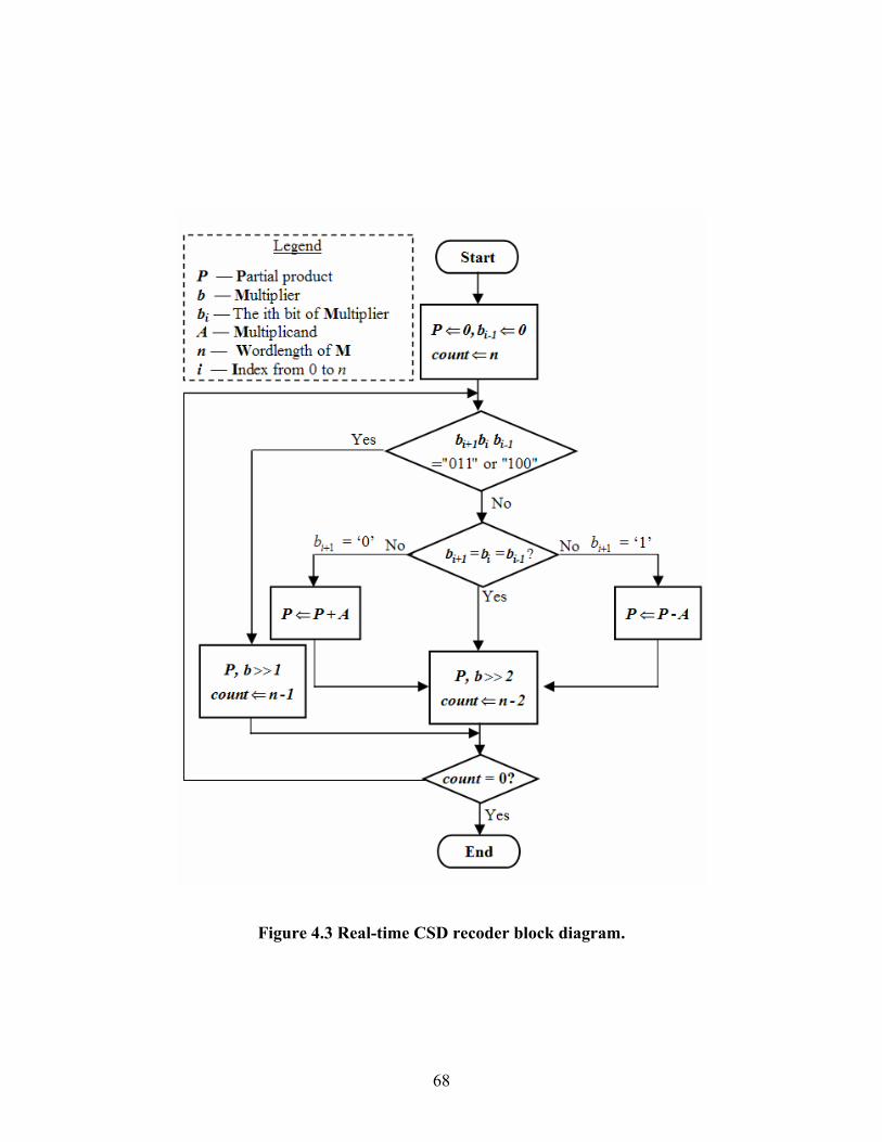
68
Figure 4.3 Real-time CSD recoder block diagram.
69
4.3 Comparison with Booth’s recoding and other CSD recoding
techniques
Recently many researchers have addressed the question of how to convert
2’s complement to CSD numbers. Some of these approaches are from the point of
view of reducing computational complexity [50], [51], but are not suitable for
implementation into hardware. Other approaches try to improve the
implementation efficiency by limiting the area and power consumption [10], [11].
However, some introduce errors, and others are still complex.
The radix-4 modified Booth’s recoding algorithm has been widely used in
modern high-speed multiplication circuits [27]. Using a modified Booth algorithm,
sequential 3-bit segments of a 2’s complement number are converted into the digit
set{ }2, 1, 0± ± . This technique reduces an n-bit 2’s complement multiplier to
2n⎡ ⎤⎢ ⎥ digits. The partial products can be readily calculated by shift/add/subtract
operations.
On average, Radix-4 Booth’s recoding results in 50% of the partial products
being zero. So, although Booth’s recoding reduces the number of 1’s in multiplier,
the reduction is less than the proposed CSD recoding. Also, after the partial
products are generated in the Booth’s recoding logic, they are all passed into the
accumulation operations, even those partial products that are zero. In this way, the
70
number of arithmetic operations in the carry-save structure is not reduced. So, there
is no decrease in speed or power consumption with this algorithm.
The proposed algorithm further reduces the number of add/subtract
operations. Unlike the modified Booth’s recoding algorithm, once the zero bits in a
CSD number are detected, there is no accumulation required. So, approximately
two thirds of the time the accumulation process is bypassed. So, the algorithm
reduces the latency of the operation, as well as the power consumption of the
circuit.
Compared with other CSD recoding techniques, such as the self-timed CSD
multiplier in [10], the structure is much simpler and faster. In [10], they calculate
their complexity to be even greater than that of Booth’s recoding because their CSD
recoder needs to propagate the carry. Also, five multiples of the multiplicand
(0, , 2 )a a± ± are required in their recoder – the same as in Booth’s recoding – in
addition to carry-in and carry-out signals. Thus, their structure is more
complicated.
The proposed real-time CSD recoding multiplier eliminates 66.7% of the
multiple generation operations, on average. For these zero bits, only shifting is
required, and there is no carry propagation at all. It can be seen that the method
offers an attractive tradeoff between operation speed and computational
complexity. The detailed performance analysis is listed in Table 4.2.
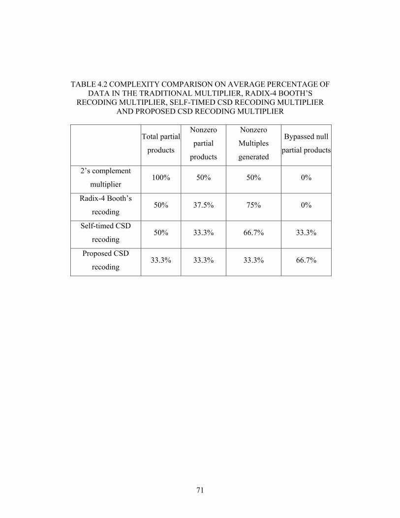
71
TABLE 4.2 COMPLEXITY COMPARISON ON AVERAGE PERCENTAGE OF
DATA IN THE TRADITIONAL MULTIPLIER, RADIX-4 BOOTH’S RECODING MULTIPLIER, SELF-TIMED CSD RECODING MULTIPLIER
AND PROPOSED CSD RECODING MULTIPLIER
Total partial
products
Nonzero
partial
products
Nonzero
Multiples
generated
Bypassed null
partial products
2’s complement
multiplier 100% 50% 50% 0%
Radix-4 Booth’s
recoding 50%
37.5% 75% 0%
Self-timed CSD
recoding 50% 33.3% 66.7% 33.3%
Proposed CSD
recoding 33.3% 33.3% 33.3% 66.7%
72
Chapter 5
EXTENSION TOPICS
In this chapter, I consider two additional topics regarding hardware
implementation of digital filters that are related to, but distinct from the main
results of this dissertation given in Chapter 3 and 4.
5.1 A multi-input CSD multiplier unit suitable for DSP algorithm
implementations
Fast operation, low power consumption and small area requirements are the
main objectives of efficient implementation of DSP algorithms in hardware [26].
Many efforts have been devoted in this area to achieve these often competing goals
[26]. Multiplication is widely used in most DSP algorithms. Multipliers are costly
in terms of chip area, power consumption and operation time [27]. However, it is
possible to avoid multiplication by using shift-and-add techniques [33]-[36]. Many
researchers have addressed the question of how to implement the multiplications
for fixed-coefficient filters to reduce the area required and power consumed [13],
73
[15], [29], [44], [54]-[56]. Some of these approaches are from the point of view of
hardware fabrication and hardware circuit design [56], for example to reduce the
short circuit and leakage currents in the CMOS circuit design, which in turn reduce
the power consumption. Other approaches try to improve the implementation
efficiency of a multiplier by reducing the number of shift/add operations [15], [44],
[55], [56], which leads to a reduction in both the power consumption and area
requirements.
One effective method of reducing the number of shift/add operations in a
multiplier is to reduce the wordlength of the multipliers. However, reducing the
wordlength can ruin the performance of the implemented algorithm [22]. For
example, reducing the number of bits in FIR filter coefficients may degrade the
filter frequency response. Another commonly used method is using alternate
number representations of the multiplier, such as CSD number system [3], [39] or
SPT representation [8].
In this section, I introduce a new multiplier structure: the multi-input CSD
multiplier unit. Since this unit does not require a fixed value for the multiplier input
to be known a priori, it has broad applications. The multi-input multiplier has
several advantages. First, since it uses CSD representation of the multiplier, it
requires fewer shift/add/subtract operations. In addition, since all the
multiplications share one CSD conversion unit, the overhead for generating the
74
control signals is reduced. Furthermore, because all the products are produced
simultaneously, the multiplication speed, and thus the filter throughput, is
improved. Also, the multiplier can be applied to efficiently implement digital filters
with non-fixed coefficients, such as adaptive filters. The implementation efficiency
can be further improved by reducing the wordlength of the input signal with little or
no sacrifice in the filter performance.
To the best of the authors’ knowledge, this is the first time that a multi-input
multiplier has been proposed as a hardware block that is suitable for DSP algorithm
applications; its advantages and applications are studied in this chapter.
5.1.1 Multi-input CSD multiplier structure
Figure 5.1 shows the proposed Multiple-input CSD multiplier with N
multiplicands 1y , 2y , … Ny and one L-bit multiplier x. This multi-input multiplier
is suitable for hardware implementation of many multiplications that have the same
multiplier but different multiplicands.
The common multiplier x is converted to CSD representation to generate
control signals by either a Look-Up-Table (LUT) or canonical recoding techniques
[40] or the new 2’s complement to CSD conversion technique [18] that has been
described in Chapter 3. The real-time CSD recoding multiplier structure [19] that
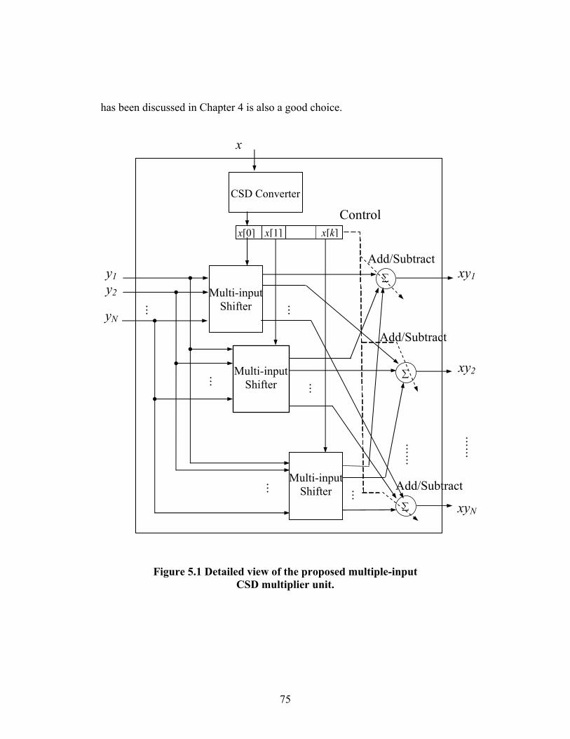
75
has been discussed in Chapter 4 is also a good choice.
Figure 5.1 Detailed view of the proposed multiple-input CSD multiplier unit.
x
CSD Converter
∑
∑
∑
Control x[0] x[1] x[k]
y1 y2
yN
xy1
xy2
xyN
Multi-input Shifter
Multi-input Shifter
Multi-input Shifter
Add/Subtract
Add/Subtract
Add/Subtract
76
The multi-input shifters use the same control signals generated by a CSD
converter; so all multiplicands are shifted by the same number of bits. Since no two
adjacent bits in a CSD number are nonzero, as a result, there are less than 2L⎡ ⎤⎢ ⎥
control signals [ ]x k ( 0 2Lk≤ ≤ ⎡ ⎤⎢ ⎥ ), where k denotes the thk nonzero digit of the
CSD representation of x . Therefore, the CSD number representation can reduce the
number of add/subtract/shift operations to less than or equal to a number that is
approximately half the number of bits in the multiplier x. To accommodate the
maximum number of nonzero digits in the CSD representation of the input sample,
this multi-input CSD multiplier structure requires 2L⎡ ⎤⎢ ⎥ shifters. Similarly,
( )12LN ⎡ ⎤ −⎢ ⎥ two-input adders (subtractors) are required to add the coefficient bit
slices.
Table 5.1 lists the number of shift-and-add operations required for the worst
case with the proposed multi-input multiplier, for a CSD based multiplier and for a
traditional binary number representation based multiplier. The shifters in the
proposed multiplier are multi-input shifters. Because these multi-input shifters
have the same control signals, some new techniques could be developed to reduce
the power consumption and area requirements of their hardware implementation.
Nevertheless, the worst case area requirement and power consumption for these
multi-input shifters is the number of inputs times the area requirement and power
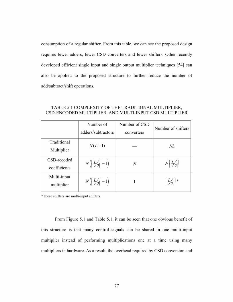
77
consumption of a regular shifter. From this table, we can see the proposed design
requires fewer adders, fewer CSD converters and fewer shifters. Other recently
developed efficient single input and single output multiplier techniques [54] can
also be applied to the proposed structure to further reduce the number of
add/subtract/shift operations.
TABLE 5.1 COMPLEXITY OF THE TRADITIONAL MULTIPLIER,
CSD-ENCODED MULTIPLIER, AND MULTI-INPUT CSD MULTIPLIER
Number of
adders/subtractors
Number of CSD
converters Number of shifters
Traditional
Multiplier ( 1)N L − — NL
CSD-recoded
coefficients ( )12
LN ⎡ ⎤ −⎢ ⎥ N 2LN ⎡ ⎤⎢ ⎥
Multi-input
multiplier ( )12LN ⎡ ⎤ −⎢ ⎥ 1 2
L⎡ ⎤⎢ ⎥ *
*These shifters are multi-input shifters.
From Figure 5.1 and Table 5.1, it can be seen that one obvious benefit of
this structure is that many control signals can be shared in one multi-input
multiplier instead of performing multiplications one at a time using many
multipliers in hardware. As a result, the overhead required by CSD conversion and
78
control signal generation can be significantly reduced. Also several multiplications
are performed simultaneously, so the overall computation speed can be improved.
The greater the number of inputs in the multi-input multiplier, the greater
the savings in hardware implementation this multiplier will achieve. Although the
advantages of this structure depend on the assumption that all these multiplications
have the same multiplier, this multi-input multiplier could have broad applications
in DSP algorithms implementation, which is illustrated in the following discussion
of applications.
5.1.2 Application to implementation of digital filters
Because digital filters have been and continue to be one of the fundamental
building blocks of many signal processing systems, the design of an efficient,
low-power FIR filter and its implementation is extremely important. It is known
that the major bottleneck of low-power FIR, or IIR, filter implementation is in the
coefficient multipliers. In addition to the studies of fixed-coefficient filters, there
has been a increasing interest in adaptable-coefficient filters or digital filters with
unknown coefficients [3], [6], [8], [13], [17]. Since the proposed multi-input
multiplier does not require a known or fixed multiplicand value, the multiplier is a
good candidate structure for efficient implementation of these digital filters.
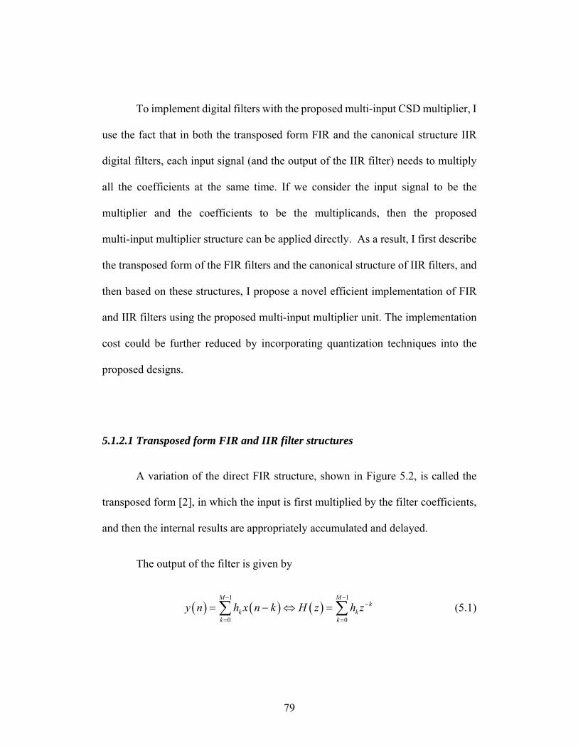
79
To implement digital filters with the proposed multi-input CSD multiplier, I
use the fact that in both the transposed form FIR and the canonical structure IIR
digital filters, each input signal (and the output of the IIR filter) needs to multiply
all the coefficients at the same time. If we consider the input signal to be the
multiplier and the coefficients to be the multiplicands, then the proposed
multi-input multiplier structure can be applied directly. As a result, I first describe
the transposed form of the FIR filters and the canonical structure of IIR filters, and
then based on these structures, I propose a novel efficient implementation of FIR
and IIR filters using the proposed multi-input multiplier unit. The implementation
cost could be further reduced by incorporating quantization techniques into the
proposed designs.
5.1.2.1 Transposed form FIR and IIR filter structures
A variation of the direct FIR structure, shown in Figure 5.2, is called the
transposed form [2], in which the input is first multiplied by the filter coefficients,
and then the internal results are appropriately accumulated and delayed.
The output of the filter is given by
( ) ( ) ( )1 1
0 0
M Mk
k kk k
y n h x n k H z h z− −
−
= =
= − ⇔ =∑ ∑ (5.1)
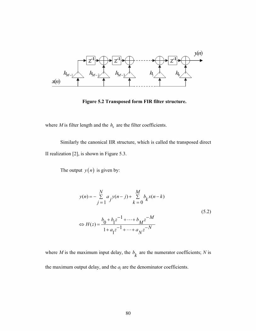
80
Figure 5.2 Transposed form FIR filter structure.
where M is filter length and the kh are the filter coefficients.
Similarly the canonical IIR structure, which is called the transposed direct
II realization [2], is shown in Figure 5.3.
The output ( )y n is given by:
( ) ( ) ( )1 0
10 1( ) 11 1
N My n a y n j b x n kj kj k
Mb b z b zMH z Na z a zN
= − − + −∑ ∑= =
− −+ + +⇔ =
− −+ + +
(5.2)
where M is the maximum input delay, the bk are the numerator coefficients; N is
the maximum output delay, and the aj are the denominator coefficients.
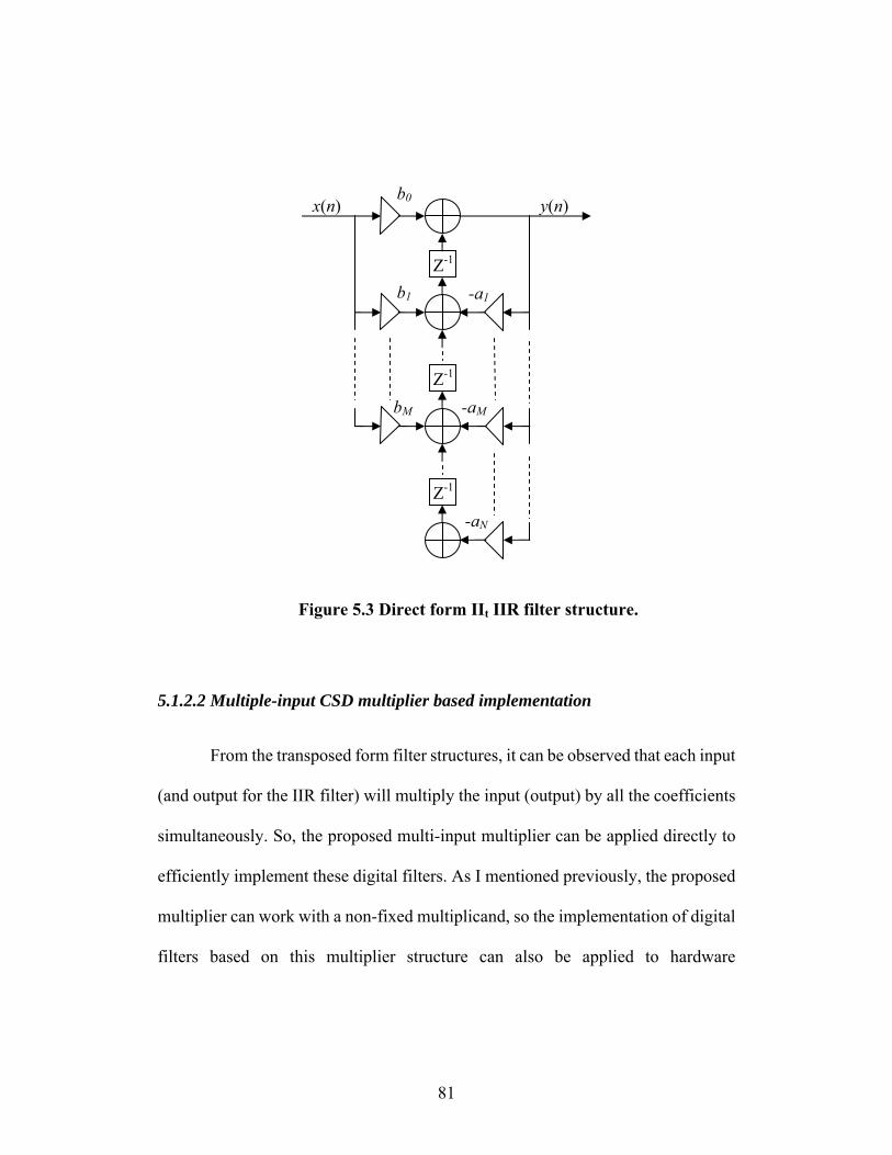
81
Figure 5.3 Direct form IIt IIR filter structure.
5.1.2.2 Multiple-input CSD multiplier based implementation
From the transposed form filter structures, it can be observed that each input
(and output for the IIR filter) will multiply the input (output) by all the coefficients
simultaneously. So, the proposed multi-input multiplier can be applied directly to
efficiently implement these digital filters. As I mentioned previously, the proposed
multiplier can work with a non-fixed multiplicand, so the implementation of digital
filters based on this multiplier structure can also be applied to hardware
Z-1
Z-1
Z-1
x(n) y(n)
b1
b0
bM
-a1
-aM
-aN
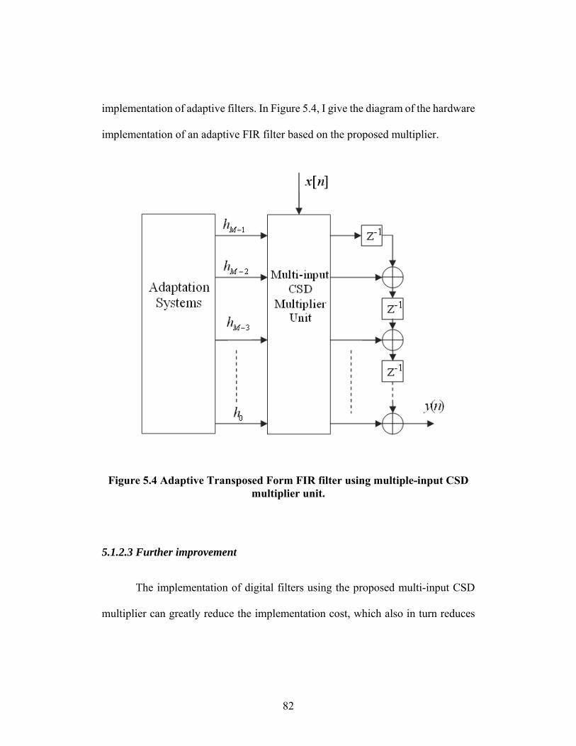
82
implementation of adaptive filters. In Figure 5.4, I give the diagram of the hardware
implementation of an adaptive FIR filter based on the proposed multiplier.
Figure 5.4 Adaptive Transposed Form FIR filter using multiple-input CSD multiplier unit.
5.1.2.3 Further improvement
The implementation of digital filters using the proposed multi-input CSD
multiplier can greatly reduce the implementation cost, which also in turn reduces
83
the area requirement and power consumption. It is well-known that the
implementation cost of multiplication can be greatly reduced by limiting the
wordlength of the multiplier. However, in a traditional filter implementation, a
reduction in the wordlength of multipliers (usually the filter coefficients) could
perturb the realized frequency response to the extent that the filter design
specification is no longer satisfied. Thus, the reduction is limited by filter
specifications [22].
However, in the proposed implementation, increasing the width of the
adders corresponds to increasing the filter coefficient wordlength. So the frequency
response error can be reduced merely by increasing the width of the adders ( which
have typically been reduced in number during the design of the frequency response
by determining the theoretical minimum filter order that is required to meet the
specification). To reduce the multiplication cost, we need to restrict the wordlength
of the filter input signals, which corresponds to Analog-to-Digital (A-D)
conversion noise. However, compared to the filter response error, the A-D noise
contributes less to the final filter output error [57]. This is the significant advantage
of the design since the number of adders that are required is equal to the number of
nonzero digits in the CSD representation of the input sample, which cannot exceed
n/2 for n-bit inputs. As a result, by increasing the width of the adders and reducing
the wordlength of the filter input signals in my implementation, implementation
cost of the digital filter can be greatly reduced with little or no sacrifice in filter
84
performance, which is confirmed by my simulation results given in Section 5.1.4.
5.1.3 Other applications
In addition to the applications of digital filter implementations, the
developed multi-input multiplier can be applied to other DSP algorithms. In Figure
5.5, I present an efficient hardware implementation of FIR filter banks using the
multi-input multiplier.
The ( )x n is the input data; ( )H ji represents the jth coefficient of ith filter;
( )iy n represents the ith filter output. The developed multi-input CSD multiplier
unit can also be applied to implement matrix multiplications, such as a matrix
multiplied by a vector or a vector times a constant. Other possible applications
include implementing digital image processing algorithms and nonlinear
polynomial filters.
5.1.4 Simulation Results
Here, I provide an FIR filter implementation example, which confirms the
techniques I introduced in Section 5.1.2.3. Consider a low-pass FIR filter with
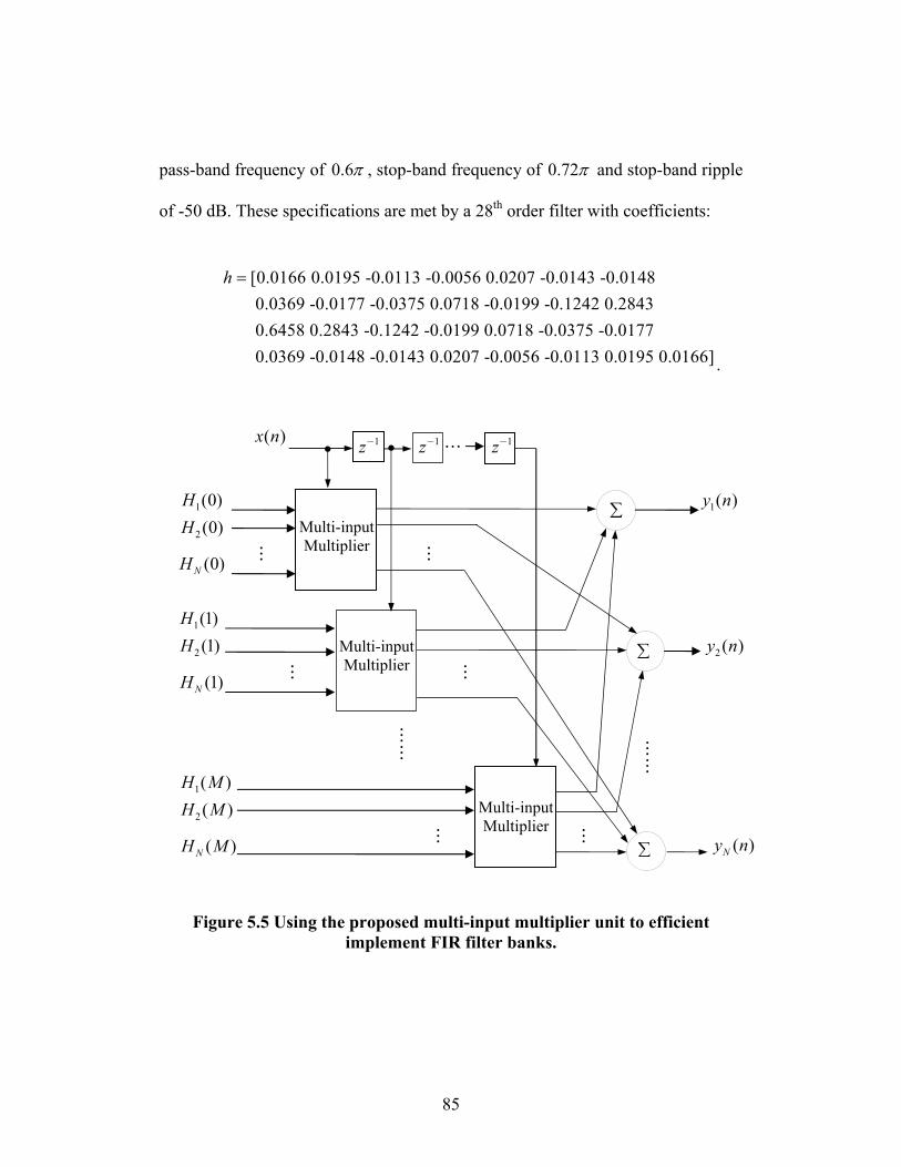
85
pass-band frequency of 0.6π , stop-band frequency of 0.72π and stop-band ripple
of -50 dB. These specifications are met by a 28th order filter with coefficients:
.
Figure 5.5 Using the proposed multi-input multiplier unit to efficient implement FIR filter banks.
[0.0166 0.0195 -0.0113 -0.0056 0.0207 -0.0143 -0.0148 0.0369 -0.0177 -0.0375 0.0718 -0.0199 -0.1242 0.2843 0.6458 0.2843 -0.1242 -0.0199 0.0718 -0.0375 -0.0177 0.0369 -0.0148 -0.0143 0.0207
h =
-0.0056 -0.0113 0.0195 0.0166]
∑
( )x n 1z− 1z− 1z−
1(0)H
2 (0)H
(0)NH
1(1)H
2 (1)H
(1)NH
1( )H M
2 ( )H M
( )NH M
∑
∑
1( )y n
2 ( )y n
( )Ny n
Multi-input Multiplier
Multi-input Multiplier
Multi-input Multiplier
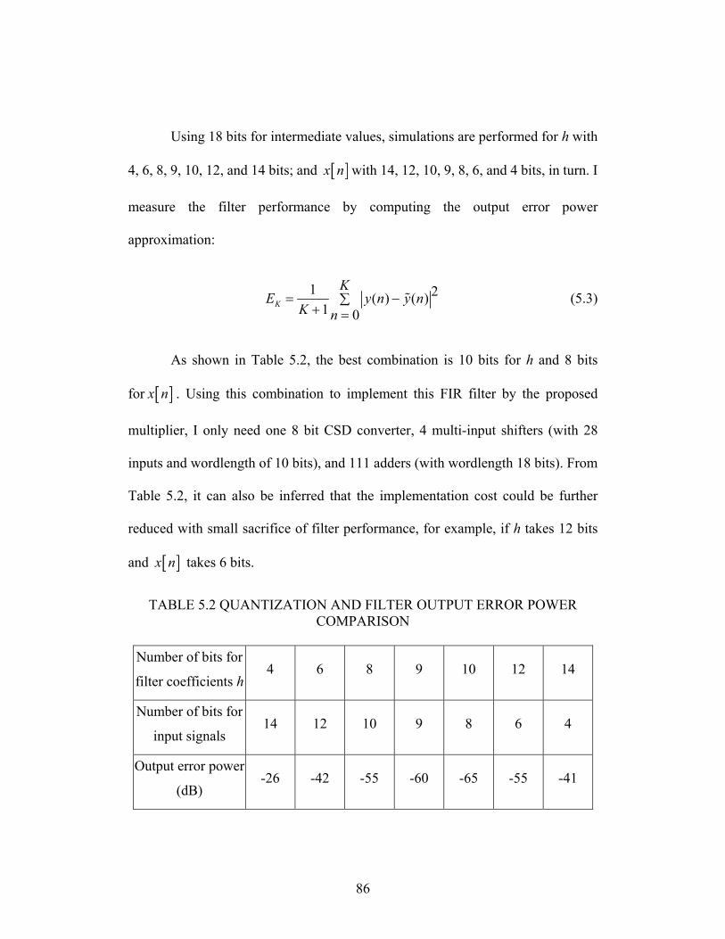
86
Using 18 bits for intermediate values, simulations are performed for h with
4, 6, 8, 9, 10, 12, and 14 bits; and [ ]x n with 14, 12, 10, 9, 8, 6, and 4 bits, in turn. I
measure the filter performance by computing the output error power
approximation:
1 2( ) ( )1 0
K
KE y n y n
K n= −∑
+ = (5.3)
As shown in Table 5.2, the best combination is 10 bits for h and 8 bits
for [ ]x n . Using this combination to implement this FIR filter by the proposed
multiplier, I only need one 8 bit CSD converter, 4 multi-input shifters (with 28
inputs and wordlength of 10 bits), and 111 adders (with wordlength 18 bits). From
Table 5.2, it can also be inferred that the implementation cost could be further
reduced with small sacrifice of filter performance, for example, if h takes 12 bits
and [ ]x n takes 6 bits.
TABLE 5.2 QUANTIZATION AND FILTER OUTPUT ERROR POWER COMPARISON
Number of bits for
filter coefficients h 4 6 8 9 10 12 14
Number of bits for
input signals 14 12 10 9 8 6 4
Output error power
(dB) -26 -42 -55 -60 -65 -55 -41
87
5.2 Optimizing filter order and coefficient length in the design of
high performance filters for high throughput FPGA
implementations
For a given filter design specification, there is generally a minimum order
that is required to meet the specification with an FIR filter; for a given specification
and order, increased quantization generally degrades performance relative to the
ideal specification. There is generally a minimum word length that is required for
the quantized filter implementation to still meet the design specification
The idea following is: compared to the filter with minimum order and
maximum quantization that meets the specification, can we increase the order and
increase the quantization simultaneously to obtain a more efficient filter that still
meets the specification?
The answer appears to be YES.
The efficiency of a hardware filter design utilizing FastCSD and the
real-time CSD recoding multiplier structure that I developed in Chapter 3 and
Chapter 4 can often be further improved reducing the required multiplier
wordlengths through an increase of the filter order beyond the minimum order that
is needed to meet the design specification.
First of all, I look at this with regard to filters having fixed coefficients that
88
are known a priori.
5.2.1 Optimizing filter order and coefficient length in the design of FIR filters
When implementing a filter using VLSI hardware, we must consider
quantization of the coefficients that make up the filter, as well as the quantization of
internal computations (both multiplications and additions) [57]. These will directly,
along with the communications or wiring diagrams, specify the hardware
requirements. The definition of the quantization function affects not only the
hardware requirements, but also the performance of the filter. The quantization of
the fixed-point coefficient values directly influences the area required by the
implementation. Quantization of the input, output and internal computations also
affects the required area. Of course, filter performance is also affected [22].
Quantization can be viewed as a many-to-one function that maps a set of real
numbers to a single value.
This way of defining quantization leads to the idea of further limiting the
range of the quantization function. For example, in filter implementations, one
could use the quantization function so that only “good” filter coefficients are
allowed. By “good,” it would mean in this case that the implementations could only
realize coefficients that are limited combinations (sums and differences) of
89
powers-of-two [35].
Some level of quantization can be imposed on the coefficients that still
allows the filter specifications to be met. However, for long filters, a savings of a
single bit can be significant and worth an increase in the order. In this section, the
order of the filter is increased to improve the filter implementation without a loss in
the performance of the filter. Similar approaches have been considered for lattice
wave digital filters [58] and much smaller filters [59].
Recently, multiplierless techniques, such as CSD number representations
[14] and dependence-graph algorithms [41] have been widely used for
implementing FIR filters in Field Programmable Gate Arrays (FPGAs). In these
implementations, rather than implementing multiplication of inputs by coefficients
using multipliers, the multiplication takes advantage of the a priori knowledge of
the coefficient values to implement the multiplication by a limited number of shifts
and adds/subtracts. To implement the shifts, a simple rewiring can be used rather
than a sequential shift register. In this way, FIR filters with known coefficients can
be implemented to operate with high-throughput and low area requirements.
Typically transpose form filters are used to achieve high-throughput because of
pipelining advantages.
90
5.2.1.1 Quantization effects on example FIR filter implementation
Usually one effective method to reduce the number of shift/add operations
in a multiplication implementation is to reduce the wordlength of the multipliers,
which are typically the coefficients in filter implementation. However, reducing the
coefficients wordlength can ruin the performance of the implemented filter
algorithm [22].
Example 5.1: Consider a non-minimum order FIR filter designed using a
generalized remez technique (firgr in MATLAB®) with the following
specifications: ωp = 0.43; ωs=0.5; Ap=0.2 dB and As=50 dB. Based on the
MATLAB® results, we find that an order of 90 with coefficients quantized
uniformly with at least 19 bits (not including the sign bit) can achieve this
specification.
Figure 5.6 shows the frequency response effects of quantizing the filter
coefficients from 19 bits to 8 bits (not including the sign bit). It can be observed that
with the decrease in the number of bits in the coefficient, the errors get bigger and
bigger.
We can calculate the filter response error power ( )fE ω for different
numbers of bits in the coefficients:
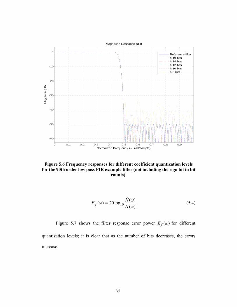
91
0 0.1 0.2 0.3 0.4 0.5 0.6 0.7 0.8 0.9
-60
-50
-40
-30
-20
-10
0
Normalized Frequency (×π rad/sample)
Mag
nitu
de (
dB)
Magnitude Response (dB)
Reference filterh 19 bitsh 14 bitsh 12 bitsh 10 bitsh 8 bits
Figure 5.6 Frequency responses for different coefficient quantization levels for the 90th order low pass FIR example filter (not including the sign bit in bit
counts).
10ˆ ( )( ) 20log
( )fHEH
ωω
ω=
. (5.4)
Figure 5.7 shows the filter response error power ( )fE ω for different
quantization levels; it is clear that as the number of bits decreases, the errors
increase.
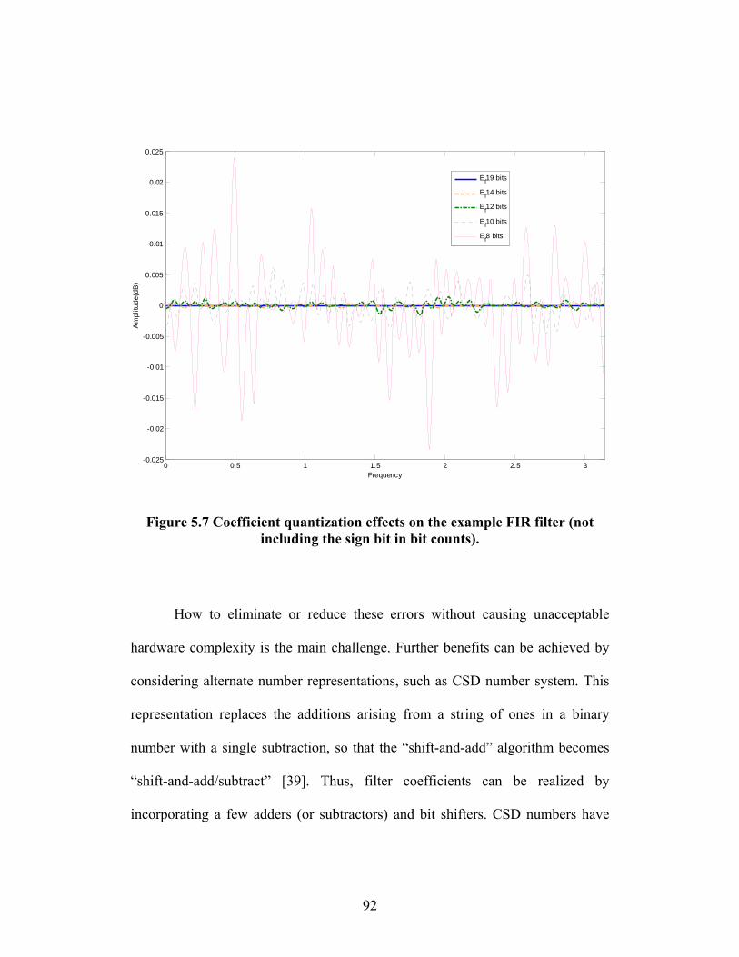
92
0 0.5 1 1.5 2 2.5 3-0.025
-0.02
-0.015
-0.01
-0.005
0
0.005
0.01
0.015
0.02
0.025
Frequency
Am
plitu
de(d
B)
Ef19 bits
Ef14 bits
Ef12 bits
Ef10 bits
Ef8 bits
Figure 5.7 Coefficient quantization effects on the example FIR filter (not including the sign bit in bit counts).
How to eliminate or reduce these errors without causing unacceptable
hardware complexity is the main challenge. Further benefits can be achieved by
considering alternate number representations, such as CSD number system. This
representation replaces the additions arising from a string of ones in a binary
number with a single subtraction, so that the “shift-and-add” algorithm becomes
“shift-and-add/subtract” [39]. Thus, filter coefficients can be realized by
incorporating a few adders (or subtractors) and bit shifters. CSD numbers have
93
proven to be useful in implementing multipliers with less complexity, because the
cost of multiplication is a direct function of the number of nonzero bits in the
multiplier, which can be reduced by using CSD numbers [37].
5.2.1.2 Optimizing the example FIR filter design by increasing the order
In general, there is a tradeoff between the hardware complexity and the
filter performance associated with the wordlength of the multipliers. Increased
coefficient wordlength increases implementation complexity, and decreased
coefficient wordlength results in greater filter response error. However, we can
increase the order of the filter to further improve the filter implementation without a
loss in filter performance. For long filters, the results are much more significant
because of the increased effect of saving a bit in each coefficient.
5.2.1.2.1 FIR filter implementations with non-minimum order designs
Consider the previous Example 5.1. The specification can be achieved with
a 90th order filter and coefficients quantized uniformly at 19 bits; however, we can
reduce the length of the quantized coefficients further by increasing the order of the
filter design as shown in Table 5.3.
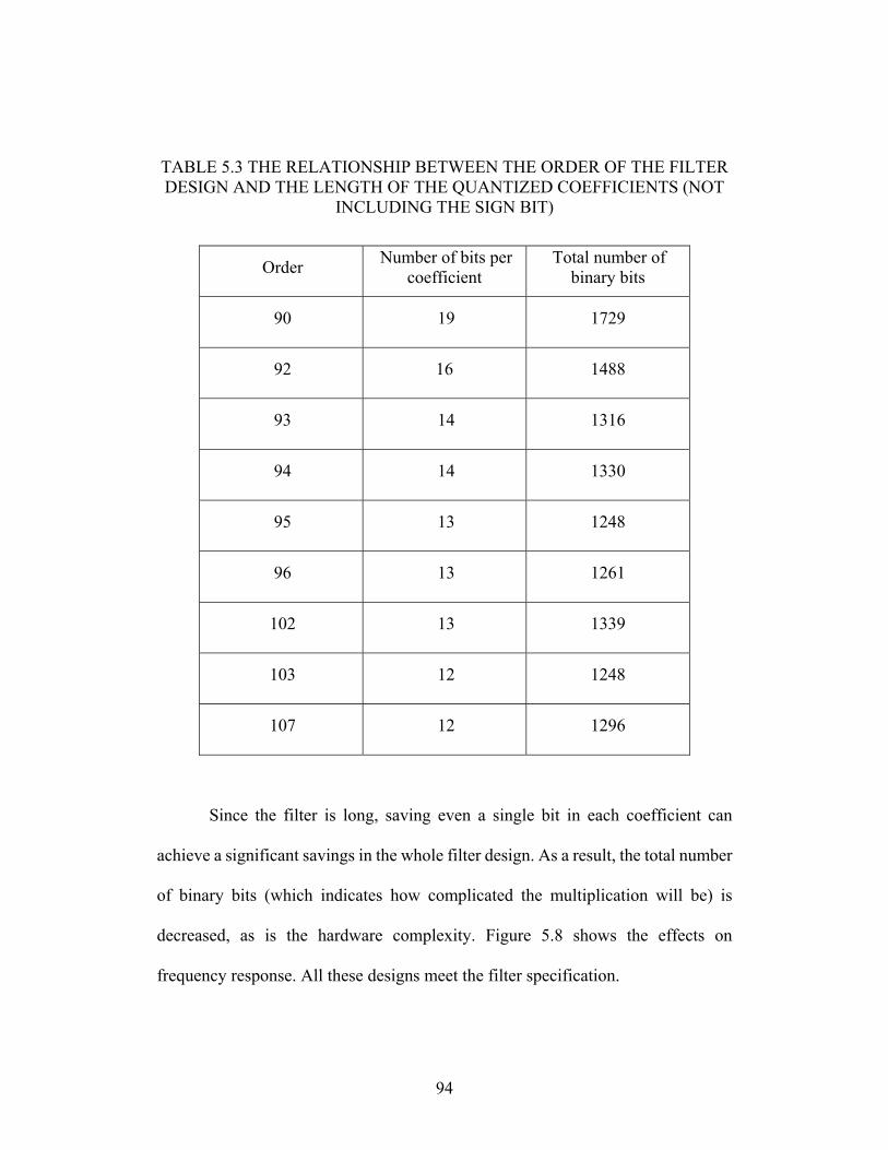
94
TABLE 5.3 THE RELATIONSHIP BETWEEN THE ORDER OF THE FILTER DESIGN AND THE LENGTH OF THE QUANTIZED COEFFICIENTS (NOT
INCLUDING THE SIGN BIT)
Order Number of bits per coefficient
Total number of binary bits
90 19 1729
92 16 1488
93 14 1316
94 14 1330
95 13 1248
96 13 1261
102 13 1339
103 12 1248
107 12 1296
Since the filter is long, saving even a single bit in each coefficient can
achieve a significant savings in the whole filter design. As a result, the total number
of binary bits (which indicates how complicated the multiplication will be) is
decreased, as is the hardware complexity. Figure 5.8 shows the effects on
frequency response. All these designs meet the filter specification.
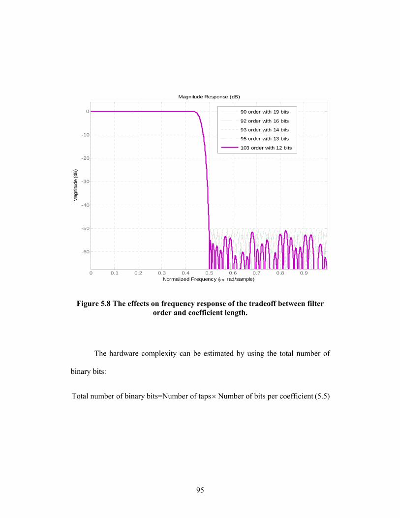
95
0 0.1 0.2 0.3 0.4 0.5 0.6 0.7 0.8 0.9
-60
-50
-40
-30
-20
-10
0
Normalized Frequency (×π rad/sample)
Mag
nitu
de (
dB)
Magnitude Response (dB)
90 order with 19 bits
92 order with 16 bits
93 order with 14 bits
95 order with 13 bits
103 order with 12 bits
Figure 5.8 The effects on frequency response of the tradeoff between filter order and coefficient length.
The hardware complexity can be estimated by using the total number of
binary bits:
Total number of binary bits=Number of taps Number of bits per coefficient× (5.5)
96
5.2.1.2.2 FIR filter implementations with increased constraints
With the same specifications: ωp = 0.43; ωs=0.5; Ap=0.2 dB, Table 5.4
summarizes the results achieved when the rejection band is lowered.
The total number of bits required for these example designs is summarized
in Table 5.4. This measure of complexity is a more generalized approach to area
requirement that would give insight into general designs. However, more accurate
area requirements for these particular filters can be determined through
implementation and/or determining the number of non-zero bits required for a CSD
implementation which is also listed in Table 5.4. As the rejection band attenuation
requirement is increased, the filter order and the number of bits per coefficient
required also increase. The results here are similar to those shown in Table 5.3:
since the filter is long, saving even a single bit in each coefficient can achieve a
significant savings in the whole filter design. As a result, when the order increased,
the total number of binary bits is decreased, as well as the total number of non-zero
CSD bits and the hardware complexity. For this example, using an increased
attenuation requirement in the design process and the original attenuation
requirement for the coefficient quantization led to an increase in the total number of
bits. It appears that this commonly used approach has significant drawbacks with
respect to implementation area.
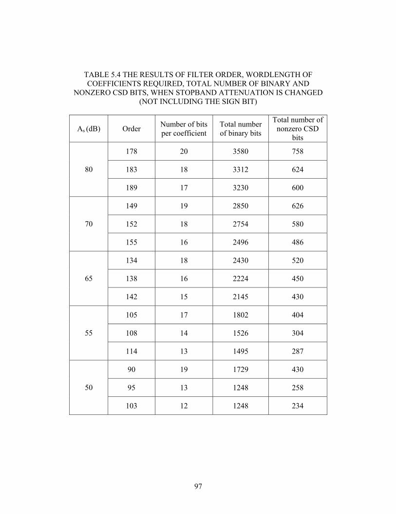
97
TABLE 5.4 THE RESULTS OF FILTER ORDER, WORDLENGTH OF COEFFICIENTS REQUIRED, TOTAL NUMBER OF BINARY AND
NONZERO CSD BITS, WHEN STOPBAND ATTENUATION IS CHANGED (NOT INCLUDING THE SIGN BIT)
As (dB) Order Number of bits per coefficient
Total number of binary bits
Total number of nonzero CSD
bits
178 20 3580 758
183 18 3312 624 80
189 17 3230 600
149 19 2850 626
152 18 2754 580 70
155 16 2496 486
134 18 2430 520
138 16 2224 450 65
142 15 2145 430
105 17 1802 404
108 14 1526 304 55
114 13 1495 287
90 19 1729 430
95 13 1248 258 50
103 12 1248 234
98
5.2.2 Optimizing filter order and coefficient length in the design of
multiplierless adaptive filters
Similar results can be obtained for adaptive systems, which is more directly
relevant to the new techniques introduced in Chapter 3 and 4 of this dissertation.
In this section, I explore the implementation of adaptive finite impulse
response (FIR) filters using VLSI hardware, such as field programmable gate
arrays (FPGAs) [53]. Typically, adaptive filters are implemented using
conventional multipliers because of the need to change the filter coefficients with
the adaptation algorithm [60]. This approach does not allow the implementation to
exploit previously existing multiplierless techniques that are appropriate only for
implementing fixed coefficient filters. The new multiplierless techniques
introduced in Chapter 3 and 4 can be used for implementing adaptive filters, but
coefficient quantization effects must be taken into consideration since most
adaptation algorithms are based on the assumption of infinite precision
coefficients.
To implement an adaptive filter using multiplierless approaches, the
possible coefficients must be significantly limited. The adaptation function must be
defined to select among this restricted set of possible coefficients. Opportunities
arise for further restriction of the set to coefficients that are particularly desirable,
e.g. powers-of-two, sums of two powers-of-two, differences of two powers-of-two.
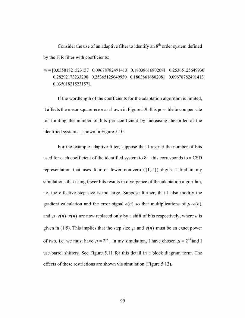
99
Consider the use of an adaptive filter to identify an 8th order system defined
by the FIR filter with coefficients:
w = [0.03501821523157 0.09678782491413 0.18038616802081 0.25365125649930 0.28292173233290 0.25365125649930 0.18038616802081 0.09678782491413 0.03501821523157].
If the wordlength of the coefficients for the adaptation algorithm is limited,
it affects the mean-square-error as shown in Figure 5.9. It is possible to compensate
for limiting the number of bits per coefficient by increasing the order of the
identified system as shown in Figure 5.10.
For the example adaptive filter, suppose that I restrict the number of bits
used for each coefficient of the identified system to 8 – this corresponds to a CSD
representation that uses four or fewer non-zero ({1, 1}) digits. I find in my
simulations that using fewer bits results in divergence of the adaptation algorithm,
i.e. the effective step size is too large. Suppose further, that I also modify the
gradient calculation and the error signal ( )e n so that multiplications of ( )e nμ ⋅
and ( ) ( )e n x nμ ⋅ ⋅ are now replaced only by a shift of bits respectively, where μ is
given in (1.5). This implies that the step size μ and ( )e n must be an exact power
of two, i.e. we must have 2 νμ −= . In my simulation, I have chosen 52μ −= and I
use barrel shifters. See Figure 5.11 for this detail in a block diagram form. The
effects of these restrictions are shown via simulation (Figure 5.12).
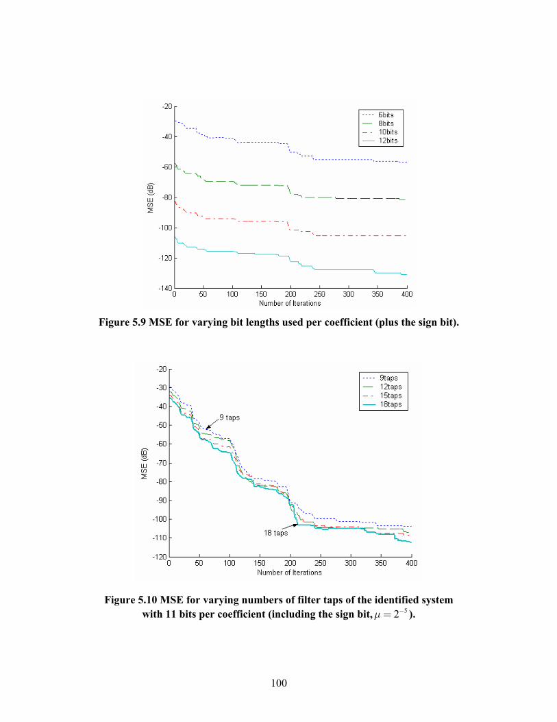
100
Figure 5.9 MSE for varying bit lengths used per coefficient (plus the sign bit).
Figure 5.10 MSE for varying numbers of filter taps of the identified system with 11 bits per coefficient (including the sign bit, 52μ −= ).
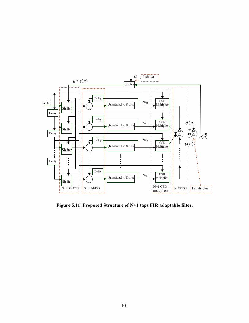
101
Figure 5.11 Proposed Structure of N+1 taps FIR adaptable filter.
μ
( )x n w0
w1
w2
wN
- +
∑ ∑
N+1 shifters N+1 adders N+1 CSD multipliers
( )y n
( )d n
N adders 1 subtractor
1 shifter
( )e n
Delay
Delay
Delay
Shifter
Shifter
Shifter
Shifter
Quantized to 8 bits
Delay
Quantized to 8 bits
Delay
Delay
Quantized to 8 bits
Delay
Quantized to 8 bits
CSD Multiplier
CSD Multiplier
CSD Multiplier
CSD Multiplier
Shifter( )e nμ ∗
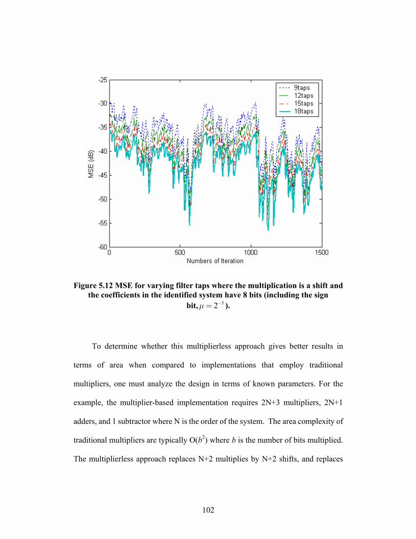
102
Figure 5.12 MSE for varying filter taps where the multiplication is a shift and the coefficients in the identified system have 8 bits (including the sign
bit, 52μ −= ).
To determine whether this multiplierless approach gives better results in
terms of area when compared to implementations that employ traditional
multipliers, one must analyze the design in terms of known parameters. For the
example, the multiplier-based implementation requires 2N+3 multipliers, 2N+1
adders, and 1 subtractor where N is the order of the system. The area complexity of
traditional multipliers are typically O(b2) where b is the number of bits multiplied.
The multiplierless approach replaces N+2 multiplies by N+2 shifts, and replaces
103
the other N+1 multiplies by combinations of shifts and additions or subtractions.
Because the shifts are not known a priori, they must be implemented using shift
registers, gates (similar to barrel shifter circuits). For a gate implementation, the
shift circuit has area complexity O(b). CSD multiplies can be implemented using
FastCSD or real-time CSD recoding multipliers as introduced in Chapter 3 and 4.
The size of each multiplier is less than or equal to O(b). So, we have replaced the
O(b2) multiplier circuits with circuits that are linear in the number of bits. Table 5.5
gives a detailed comparison between multiplier based and multiplierless adaptive
FIR filter implementation.
In summary, the area of our proposed multiplierless adaptive FIR filter design
is O(Nb) compared to the required area of a multiplier-based adaptive filter, which
is O(Nb2). Additional restrictions in the quantization function can further reduce
the area required.
TABLE 5.5 COMPLEXITY COMPARISON OF MULTIPLIER-BASED AND
MULTIPLIERLESS ADAPTIVE FIR FILTERS OF ORDER N
Number of
b-bit multipliers
Number of b-bit adders
Number of b-bit
subtractors
Number of shift circuits
Number of CSD
multiplies
Multiplier-based 2N+3 2N+1 1 — —
Multiplierless — 2N+1 1 N+2 N+1
104
Chapter 6
CONCLUSIONS AND FUTURE WORKS
6.1 Conclusions
I have reviewed current filter implementation techniques and multiplierless
techniques for high performance FPGA implementation of digital filters in this
dissertation. Current popular multiplierless techniques have been implemented and
compared in detail by designing an example loop filter in Delta-Sigma A/D and
D/A system.
The implementation of adaptive filters cannot benefit from fast, low area
filter design techniques that use a priori information about the filter coefficients. I
propose a novel implementation technique — FastCSD that can be used to
construct general multipliers which require less area and achieve higher throughput
rates. The method for converting a number from 2’s complement representation to
CSD representation can be used to implement adaptive filters in FPGAs or other
custom hardware. Performance analysis indicates that the design provides better
results than are currently available considering both the conversion speed and the
105
computational complexity. Since the technique does not require a specific word
length for the multiplier and does not depend on prior knowledge of the multiplier
value, it has broad applications. The method only requires several shifts and logic
operations, so the complexity of the hardware implementation has been effectively
reduced compared to conventional methods, such as modified Booth’s recoding
and Look-Up-Table based techniques. The throughput of the implementation can
be further improved by incorporating parallel processing with only a modest
increase in area [18].
I have presented an efficient iterative multiplier structure based on a novel
real-time CSD recoding circuit [19], [20]. To the best of my knowledge, this
structure is the first iterative multiplier based on real-time CSD recoding. Because
of the iterative multiplier nature, the proposed design requires lower area compared
with array multipliers. Furthermore, the CSD number property ensures that this
multiplier has the minimum number of nonzero partial products among all radix-2
number representation based multipliers. The number of add/subtract operations is
further reduced through the use of bypass techniques. On average, 66.7% of the
partial product generation operations are replaced with a simple bypass to the
shifting structure and carry propagation is totally eliminated as well. Thus, the
complexity of the hardware implementation is dramatically reduced as compared to
conventional methods, including modified Booth recoding and competing CSD
recoding techniques. This approach achieves an overall speed-up as well as reduced
106
power consumption which is particularly critical in mobile multimedia applications.
Finally, unlike other CSD number based multipliers, the structure proposed here
uses real time CSD recoding, and does not require a fixed value for the multiplier
input to be known a priori; as a result, the proposed multiplier can be used for the
efficient implementation of digital filters with non-fixed filter coefficients, such as
adaptive filters.
Also, I have presented a novel multi-input CSD multiplier unit and its
application to efficient implementation of DSP algorithms, such as the
implementations of digital filters and filter banks [53]. The developed multi-input
CSD multiplier requires less shift/add/subtract operations and CSD conversion
overhead. Consequently, the power consumption and area requirement of the
implemented hardware can be significantly reduced. The technique does not
depend on prior knowledge of the coefficients; therefore, it is suitable for adaptive
filter implementation. The implementation efficiency can be further improved by
reducing the number of input bits without any or with only a small sacrifice in the
filter performance.
Hardware complexity is one of the most important considerations when
implementing digital filter structures in FPGAs. In my dissertation, the tradeoff
between filter order and coefficient length in the design and implementation of
high-performance filters has been presented. Non-minimum order FIR filters are
107
designed for implementation using canonical signed digit (CSD) multiplierless
implementation techniques. By using non-minimum order designs, the length of the
coefficients can be reduced, and thus an overall hardware savings can be achieved.
In addition, I consider the use of overly-stringent specifications combined with
quantization and increased order to improve the filter implementation [22]. In
addition, the FPGA implementation of a multiplierless FIR adaptive filter has been
discussed [53]. Simulations of an adaptive filter were conducted, taking into
account the wordlength of each coefficient, multiply, and addition/subtraction.
Also considered is the filter tap length. The results show that one can compensate
for limiting the number of bits used to represent each coefficient by increasing the
order of the identified system. Because the proposed method produces a space
requirement that is linear in the order, rather than the conventional quadratic in the
order, I have thus effectively reduced the complexity of the hardware
implementation.
This dissertation makes the following contributions:
• Developed the first non-iterative hardware algorithm to convert 2’s
complement to CSD (FastCSD) [18] which is faster than existing
techniques with lower space and power consumptions.
• Leveraged FastCSD [18] to develop a new, high performance iterative
multiplier structure based on novel real-time CSD recoding [19], [20]
108
which has simpler structure than other competitive techniques with less
computational complexity and low power consumptions.
• Developed the first multi-input multiplier unit suitable for adaptive DSP
algorithm implementations [21].
• Optimized filter order and coefficient length for design of high performance
FIR and adaptive filters [22].
6.2 Future works
I plan to incorporate the FastCSD method [18] into the multi-input CSD
multipliers [53] which requires all the CSD digits to be converted simultaneously.
This new multi-input CSD multiplier circuit will allow the construction of high
throughput adaptive filters in FPGAs or other custom hardware under practical
time, space and power constraints.
In this dissertation, I introduced a novel radix-2 CSD iterative multiplier
that implicitly converts 2’s complement to CSD in real-time. However, it would be
interesting to explore higher radix hardware that might further reduce the power
consumption while simultaneously increasing the computational bandwidth
significantly.

109
I would also like to apply FastCSD and real-time CSD recoding multiplier
to Delta-Sigma systems. Hopefully, it will yield a higher resolution and higher
throughput D/A converter.
I also plan to evaluate the new techniques described in this dissertation and
integrate them with my previous work, such as, adaptive nonlinear filter for
adaptive nonlinear echo cancellation in [61] or the adaptive filters considered in
[53], [62], [63], and [64].
110
REFERENCES
[1] G. R. Goslin, "Using Xilinx FPGAs to Design Custom Digital Signal
Processing Devices,” Proc. of the DSPX, 1995, pp. 565-604.
[2] S. K. Mitra, Digital Signal Processing: A Computer-Based Approach, New
York: McGraw-Hill Companies, 2000.
[3] S. Haykin, Adaptive filter theory, 4th ed, New York: Prentice Hall, 2002.
[4] J. Kang and J. Gaudiot, “A simple high-speed multiplier design, ” IEEE
Trans. on Computers, vol. 55, No. 10, 2006, pp. 1253-1258.
[5] A. Efthymiou, W. Suntiamorntut, J. Garside, and L.E.M. Brackenbury,
“An Asynchronous, iterative implementation of the original Booth
multiplication algorithm,” in Proc. Int'l. Symp. Asynch. Circuits and Syst.,
2004, pp. 207-215.
[6] M. A. Soderstrand, "CSD multipliers for FPGA DSP applications," in Proc.
IEEE Int’l. Symp. Circuits, Syst., vol.5, 2003, pp. V-469 - V-472.
[7] J. Hensley, A. Lastra, and M. Singh, “An area- and energy efficient
Asynchronous Booth multiplier for mobile devices,” in Proc. IEEE Int’l.
Conf. Computer Design, 2004, pp. 18-25.
111
[8] C.-L. Chen, K.-Y. Khoo, and A. N. J. Willson, "A Simplified signed
powers-of-two conversion for multiplierless adaptive filters," in Proc.
IEEE Int’l. Symp. Circuits, Syst., 1996, pp. 364-367.
[9] G. K. Ma and F. J. Taylor, “Multiplier policies for digital signal
processing,” IEEE ASSP Mag., 1990, pp. 6-20.
[10] G.A. Ruiz and M.A. Manzano, "Self-Timed Multiplier Based on Canonical
Signed-Digit Recoding," IEE Proc. Circuits, Devices, and Systems, vol.
148, no. 5, 2001, pp. 235-241.
[11] S. M. Kim, J. G. Chung, and K. K. Parhi, “Design of low error CSD
fixed-width multiplier,” in Proc. IEEE Int’l. Symp. Circuits, Syst., 2002, pp.
I-69 - I-72.
[12] A.D. Booth, “A Signed Binary Multiplication Technique,” Quarterly J.
Mechanics and Applied Math., vol. 4, 1951, pp. 236-240.
[13] D. J. Allred, H. Yoo, V. Krishnan, W. Huang, and D. V. Anderson, "A
novel high performance distributed arithmetic adaptive filter
implementation on an FPGA," in Proc. IEEE Int’l. Conf. Acoust., Speech,
Signal Proc., vol.5, 2004, pp. V-161 - V-164.
[14] K.K. Parhi, VLSI Digital Signal Processing Systems: Design and.
Implementation, John Wiley, 1999.
112
[15] A. G. Dempster and M. D. Macleod, "Constant integer multiplication using
minimum adders," IEE Proceedings: Circuits, Devices and Systems, vol.
141, 1994, pp. 407-413.
[16] D. B. Bull and D. H. Horrocks, "Primitive operator digital filters," IEE
Proceedings, Part G: Circuits, Devices and Systems, vol. 138, 1991, pp.
401-412.
[17] D. Li and Y. C. Lim, "Multiplierless realization of adaptive filters by
nonuniform quantization of input signal," in Proc. IEEE Int’l. Symp.
Circuits, Syst., 1994, pp. 457-459.
[18] Y. Wang, L. S. DeBrunner, D. Zhou, and V. E. DeBrunner, "A novel
hardware implementation method for adaptive filter coefficients," in Proc.
IEEE Int’l. Conf. Acoust., Speech, Signal Proc., 2007.
[19] Y. Wang, L. S. DeBrunner, D. Zhou, and V. E. DeBrunner, "A multiplier
structure based on a novel real-time CSD recoding," in Proc. IEEE Int’l.
Symp. Circuits, Syst., 2007.
[20] Y. Wang, L.S. DeBrunner, D. Zhou, V.E. DeBrunner, and J. P. Havlicek,
“Efficient iterative multiplier structure based on a novel real-time CSD
recoding,” submitted to IEEE Trans. Circuits and Systems I, 2007.
[21] Y. Wang, L. DeBrunner, V. DeBrunner, and D. Zhou, “A multi-input
multiplier unit suitable for adaptive DSP algorithm implementations,” in
Proc. Asilomar Conf. Signals, Syst., Comput., 2006.
113
[22] L. S. DeBrunner and Y. Wang, "Optimizing filter order and coefficient
length in the design of high performance FIR filters for high throughput
FPGA implementations,” IEEE DSP Workshop, 2006, pp. 608-612.
[23] Berkeley Design Technology Inc., 2000, white paper, “Choosing a DSP
Processor”. http://www.bdti.com/articles/choose_2000.pdf
[24] L. Adams, "Choosing the right architecture for real-time signal processing
designs," Texas Instruments, 2002.
[25] Altera Corp., 2007, white paper, "FPGA vs. DSP Design Reliability and
Maintenance". http://www.altera.com/literature/wp/wp-01023.pdf
[26] U. Meyer-Baese, Digital Signal Processing with Field Programmable
Gate Arrays, Springer-Verlag, Berlin, Germany, 2001.
[27] B. Parhami, Computer Arithmetic: Algorithms and Hardware Designs.
London, Oxford Press, 1999.
[28] I. Koren, Computer Arithmetic Algorithms, 2nd ed., Prentice Hall, 2001.
[29] K. Chapman, “Building high performance FIR filter using KCM,” Xilinx
Ltd, 1996.
[30] G. Goslin, “A guide to using field programmable gate arrays (FPGAs) for
application-specific digital signal processing performance,” XILINX Inc.,
1995.
[31] G. Goslin, “Using Xilinx FPGAs to design custom digital signal
processing devices,” in Proceedings of the DSPX, 1995, pp. 565-604.
114
[32] O. L. MacSorley, "High Speed Arithmetic in Binary Computers", Proc. of
IRE, vol.49, no. 1, Jan. 1961. pp. 67-91.
[33] R. C. Agarwal and R. Sudhakar “Multiplier-Less Design of FIR Filters,” in
Proc. IEEE Int’l. Conf. Acoust., Speech, Signal Proc, 1983, pp. 209-212.
[34] N. Benvenuto , L. E. Franks and F. S. Hill “On the Design of FIR Filters
with Power-of-two Coefficients,” IEEE Trans. on Communications, vol.
COM-32, 1974, pp. 1299.
[35] D. Koo and A. Miron “Design of Mulitplierless FIR Digital Filters with
Two to the N th Power Coefficients,” IEEE Trans. on Consumer
Electronics, vol. CE-33, Iss. 3, 1987, pp. 109 - 114.
[36] I. A. Shah and A. K. Bhattacharya, “A Fast Multiplierless Architecture for
General Purpose VLSI FIR Digital Filters,” IEEE Trans. on Consumer
Electronics, vol. CE-33, Iss. 3, 1987, pp. 129 - 135.
[37] H. Samueli, "The design of multiplierless digital data transmission filters
with powers-of-two coefficients," in Proc. IEEE Int. Telecommunications
Symp., 1990, pp.425–429.
[38] A. G. Dempster and M. D. Macleod, “Generation of signed-digit
representations for integer multiplication,” IEEE Signal Process. Lett., vol.
11, no. 5, 2004, pp. 663-665.
[39] P. Pirsch, Architectures for Digital Signal Processing, New York: Wiley,
1998.
115
[40] G.W. Reitwiesner, “Binary Arithmetic,” Advances in Computers, vol. 1,
1960, pp. 231-308.
[41] Y. Voronenko and M. Püschel, "Multiplierless Multiple Constant
Multiplication," ACM Transactions on Algorithms. vol. 3, Iss. 2, 2007.
[42] P. R. Cappello, and K. Steiglitz, "Some complexity issues in digital signal
processing," IEEE Trans. Acoust., Speech, Signal Proc., vol. 32, no. 5,
1984, pp. 1037-1041.
[43] O. Gustafsson, A. G. Dempster, and L. Wanhammar, "Extended results for
minimum-adder constant integer multipliers," in Proc. IEEE Int’l. Symp.
Circuits, Syst., vol. 1, 2002, pp. I-73 - I-76.
[44] A. G. Dempster and M. D. Macleod, “Use of minimum-adder multiplier
blocks in FIR digital filters,” IEEE Trans. Circuits Syst. II, vol. 42, 1995,
pp. 569-577.
[45] P.M. Aziz, H.V.Sorensen, J. vn der Spiegel, "An overview of sigma-delta
converters," IEEE Signal Processing Magazine, vol. 13, Iss. 1, 1996, pp.
61 -84.
[46] D. P. Scholnik, “A parallel digital architecture for delta-sigma
modulation,” in Proc. IEEE Int'l Midwest Symp. Circuits, Syst., vol.1, 2002,
pp. I-352 - I-355.
116
[47] Y. Wang, “Multiplierless implementation of loop filters in parallel
Delta-sigma D/A converters,” Technical Report, Dept. of Electrical and
Computer Engineering, U. of Oklahoma, 2007.
[48] Y. Voronenko, "SPIRAL multiplier block generator," Carnegie Mellon U.,
2006. http://www.ece.cmu.edu/~yvoronen/homepage/mcm/gen.html
[49] John Treichler, plenary comments, IEEE DSP Workshop, 2006.
[50] F. Xu, C. Chang and C. Jong, “HWP: a new insight into canonical signed
digit,” in Proc. IEEE Int’l. Symp. Circuits, Syst., 2004, pp. 201-204.
[51] R. Hashemian, “A new method for conversion of a 2's complement to
canonic signed digit number system and its representation,” in Proc.
Asilomar Conf. Signals, Syst., Comput., 1997, pp.904-907.
[52] Bill Allaire and Bud Fischer, “Block adaptive filter,” Xilinx Application
Note, XAPP 055, version 1.1, 1997.
[53] L. S. DeBrunner, Y. Wang, V. DeBrunner, and M. Tull, "Multiplierless
implementations of adaptive FIR filters," in Proc. Asilomar Conf. Signals,
Syst., Comput., 2003, pp. 2232-2236.
[54] K. Dabbagh-Sadeghipour and A. Aghagolzadeh, “A new hardware
efficient, low power FIR digital filter implementation approach,” in Proc.
IEEE Int'l Conf. Electronics, Circuits and Syst., vol.3, 2003, pp. 1144 -
1147.
117
[55] D. Li, “Minimum number of adders for implementing a multiplier and its
application to the design of multiplierless digital filters,” IEEE Trans.
Circuits and Systems, vol. 42, Iss. 7, 1995, pp.453 – 460.
[56] H. R. Mehrvarz and C. Y. Kwok, “ A novel multi-input floating-gate MOS
four-quadrant analog multiplier,” IEEE J. of Solid-State Circuits, vol. 31,
no. 8, 1996, pp. 1123-1131.
[57] D. Chan and L. Rabiner, "Analysis of quantization errors in the direct form
for finite impulse response digital filters," IEEE Trans. on Audio and
Electroacoustics , vol. 21, 1973, pp. 354-366.
[58] Pontus Åström, Peter Nilsson and Mats Torkelsson, “Low Power
Optimization of Bit-Serial Digital Filters,” ASIC Conference and Exhibit,
1997, pp. 229 – 232.
[59] K. Tan, W. F. Leong, S. Kadam, M.A. Soderstrand, and L. G. Johnson,
“Public-domain MATLAB program to generate highly optimized VHDL
for FPGA Implementation,” in Proc. IEEE Int’l. Conf. Acoust., Speech,
Signal Proc., 2001, pp. 514 – 517.
[60] D. T. Franco and L. Carro, "A FPGA Version of a Non-Linear Adaptive
Filter," XII Symp. Integrated Circuits and Systems Design, 1999,
pp.128-131.
118
[61] D. Zhou, Y. Wang, V. DeBrunner, and L. DeBrunner, “Sub-band
Implementation of Adaptive Nonlinear Filter for Adaptive Nonlinear Echo
Cancellation,” J. Multimedia, vol. 2, Iss. 2, 2007, to appear.
[62] Y. Wang, L.S. DeBrunner, J. P. Havlicek and D. Zhou, "Signal Exclusive
Adaptive Average Filter in Impulse Noise Suppression," IEEE Southwest
Symp. Image Analysis and Interpretation, 2006. pp. 51-55.
[63] Y. Wang, L. S. DeBrunner, V. E. DeBrunner, and D. Zhou, "Quantization
effect on phase response and its application to multiplierless ANC," in Proc.
IEEE Int’l. Conf. Acoust., Speech, Signal Proc., vol. 5, 2004, pp. 65-68.
[64] D. Zhou, V. DeBrunner, L. DeBrunner and Y. Wang, "Geometric Based
analysis of FXLMS algorithm," IEEE Statistic Signal Processing 13th
Workshop, July, 2005, pp. 127-132.
119
APPENDIX A
NOMENCLATURES AND ABBREVIATIONS
⎡ ⎤⎢ ⎥
IIt
ΔΣ
A/D
D/A
Ap
As
ANC
ASICs
BHA
BHM
Round towards positive infinity
The transpose of direct form II
Delta-sigma
Analog to digital
Digital to analog
Pass band Attenuation
Stop band Attenuation
Active Noise Control
Application Specific Integrated Circuits
Bull-Horrocks’ algorithm
Bull-Horrocks’ algorithm Modified
120
CM
CMOS
CSD
DA
DAG
DFS
DSP
FFT
FIR
IIR
FPGA
IOBs
KCM
LMS
LSB
Constant Multiplication
Complementary Metal Oxide Silicon
Canonical Signed Digit
Distributed Arithmetic
Directed Acyclic Graph
Difference Form Signed
Digital signal processing
Fast Fourier Transform
Finite Impulse Response
Infinite Impulse Response
Field Programmable Gate Array
Input Output Blocks
Constant Coefficients Multiplier
Least Mean Square
Least Significant Bit
121
LUT
MAC
MAG
MCM
MSD
MSE
NRL
RAG-n
RAM
SCM
SNR
SPT
VLSI
ωp
ωs
Look Up Table
Multiply-Accumulator
Multiplier Adder Graph
Multiple Constant Multiplication
Minimal Signed Digit
Mean Squared Error
Naval Research Laboratory
n-Dimensional Reduced Adder Graph
Random Access Memory
Single Constant Multiplication
Signal-to-noise ratio
Signed Powers-of-Two
Very Large Scale Integration
Pass band Frequency
Stop band Frequency
122
APPENDIX B
SELECTED MATLAB® CODES
1. Codes that generate Figure 3.8 init fc=0.25; % center frequency B=0.015; % one-sided bandwidth fL=fc-B/2; fH=fc+B/2; % edge frequencies [hopt, delta]=SDfilter_l1([1 0 1.3125 repmat(NaN,1,197)],[fc-B/2, fc+B/2],2.95,'sedumi'); h_n0=[]; N_n0=[]; for i=1:length(hopt) if hopt(i)~=0 h_n0=[h_n0 hopt(i)]; N_n0=[N_n0 i]; end end h_n0 N_n0 h1= dfilt.dffir(hopt); hopt1=copy(h1); wl=20; set(hopt1,'Arithmetic','fixed') set(hopt1,'CoeffWordLength',wl); H_1=get(hopt1,'Numerator'); figure freqz(H_1,1) N1=hopt1.CoeffWordLength hopt2=copy(h1); wl2=input ('Coefficients Wordlength w2='); set(hopt2,'Arithmetic','fixed') set(hopt2,'CoeffWordLength',wl2); H_2=get(hopt2,'Numerator'); figure freqz(H_2,1) N2=hopt2.CoeffWordLength; hopt3=copy(h1); wl3=input ('Coefficients Wordlength w3='); set(hopt3,'Arithmetic','fixed') set(hopt3,'CoeffWordLength',wl3); H_3=get(hopt3,'Numerator'); N3=hopt3.CoeffWordLength;
123
hopt4=copy(h1); wl4=input ('Coefficients Wordlength w4='); set(hopt4,'Arithmetic','fixed') set(hopt4,'CoeffWordLength',wl4); H_4=get(hopt4,'Numerator'); N4=hopt4.CoeffWordLength; H_1max=max(abs(H_1)); np=ceil(log2(H_1max)); H1_shift=ceil(H_1*2^(N1-2)) H1_n0=[]; N1_n0=[]; for i=1:length(H1_shift) if H1_shift(i)~=0 H1_n0=[H1_n0 H1_shift(i)]; N1_n0=[N1_n0 i]; end end H1_n0 N1_n0 hopt1_csd=zeros(length(H1_n0),N1+1); r=[]; for ii=1:length(H1_n0) [hopt1_csd(ii,:),r(ii)]=real2csd(H1_n0(ii),N1,0); end; non0=sum(sum(abs(hopt1_csd))) hopt1_csd href1 = reffilter(h1);% Reference double-precision floating-point filter. hfvt1 = fvtool(href1,hopt1,hopt2,hopt3,hopt4); set(hfvt1,'ShowReference','off'); % Reference already displayed once legend(hfvt1, ['H double-precision'], ['H ' num2str(N1) ' bits'],['H ' num2str(N2) ' bits'],['H ' num2str(N3) ' bits'],['H ' num2str(N4) ' bits']) set(hfvt1, 'Color', [1 1 1]) 2. Codes that generate Figure 5.6-5.7 Wp = 0.43; Ws = 0.5; % Fc = (Fp+Fst)/2; Transition Width = Fst - Fp Ap = 0.2; As = 50; min_order=90; deltp=1-10^(-Ap/20); delts=10^(-As/20); pass= 0:1/512:Wp;
124
stop= Ws:1/512:1; [b_m,err_m]=firgr('minorder',[0 Wp Ws 1], [1 1 0 0], [deltp delts]); [H_m,W_m]=freqz(b_m,1); [b,err]=firgr(min_order,[0 Wp Ws 1], [1 1 0 0], [deltp delts]); [H_inf,W]=freqz(b,1); if sum(abs(H_inf(1:round(512*Wp)))> (1+deltp))|sum(abs(H_inf(1:round(512*Wp)))< (1-deltp)) error('(H_inf passband does not satisfy the design specification)') end tt=sum(abs(H_inf(ceil(512*Ws)+1:512))> delts); if tt>0 error('(H_inf stopband does not satisfy the design specification)') end h0 = dfilt.dffir(b); h=copy(h0); set(h,'Arithmetic','fixed') h.CoeffWordLength=19; hh=get(h,'Numerator'); [h16,W16]=freqz(hh,1); h1 = copy(h); h1.CoeffWordLength = 14; h_1=get(h1,'Numerator'); [H1,W23]=freqz(h_1,1); h2 = copy(h); h2.CoeffWordLength = input ('Estimated h coefficeints wordlength (1) ='); %h2.CoeffWordLength = 21; h_2=get(h2,'Numerator'); [H2,W21]=freqz(h_2,1); h3 = copy(h); h3.CoeffWordLength = input ('Estimated h coefficeints wordlength (2) ='); %h3.CoeffWordLength = 22; h_3=get(h3,'Numerator'); [H3,W22]=freqz(h_3,1); h4 = copy(h); h4.CoeffWordLength = input ('Estimated h coefficeints wordlength (3) ='); h_4=get(h4,'Numerator'); [H4,W24]=freqz(h_4,1); href = reffilter(h0); % Reference double-precision floating-point filter. hfvt = fvtool(href,h,h1,h2,h3,h4); set(hfvt,'ShowReference','off'); % Reference already displayed once legend(hfvt, 'Reference filter', 'h 19 bits', ['h ' num2str(h1.CoeffWordLength) ' bits'],['h ' num2str(h2.CoeffWordLength) ' bits'],['h ' num2str(h3.CoeffWordLength) ' bits'],['h ' num2str(h4.CoeffWordLength) ' bits']) set(hfvt, 'Color', [1 1 1]) diff_h19=H_inf-h16; diff_h14=H_inf-H1; diff_h2=H_inf-H2; diff_h3=H_inf-H3;
125
diff_h4=H_inf-H4; figure(2) plot(W,diff_h19) hold on plot(W,diff_h14,'y--') hold on plot(W,diff_h2,'g-.') hold on plot(W,diff_h3,'k:') hold on plot(W,diff_h4,'m') xlabel('Frequency') ylabel('Amplitude(dB)') legend('E_f19 bits','E_f14 bits','E_f12 bits','E_f10 bits','E_f8 bits'); 3. Codes that generate Figure 5.8 Wp = 0.43; Ws = 0.5; % Fc = (Fp+Fst)/2; Transition Width = Fst - Fp Ap = 0.2; As = 50; min_order=95; deltp=1-10^(-Ap/20); delts=10^(-As/20); [b,err]=firgr(min_order,[0 Wp Ws 1], [1 1 0 0], [deltp delts]); [H_inf,W]=freqz(b,1); h0 = dfilt.dffir(b); h=copy(h0); set(h,'Arithmetic','fixed') h1 = copy(h); h1.CoeffWordLength = 19; H_1=get(h1,'Numerator') H_1max=max(abs(H_1)); np=ceil(log2(H_1max)); if np<0 np=0; end p1=92; [bp1,errp1]=firgr(p1,[0 Wp Ws 1], [1 1 0 0], [deltp delts]); hp1= dfilt.dffir(bp1); set(hp1,'Arithmetic','fixed') Ht(1)=copy(hp1); set(Ht(1),'CoeffWordLength',16); p2=93; [bp2,errp2]=firgr(p2,[0 Wp Ws 1], [1 1 0 0], [deltp delts]);
126
hp2 = dfilt.dffir(bp2); set(hp2,'Arithmetic','fixed') Ht(2)=copy(hp2); set(Ht(2),'CoeffWordLength',14); p3=95; [bp3,errp3]=firgr(p3,[0 Wp Ws 1], [1 1 0 0], [deltp delts]); hp3 = dfilt.dffir(bp3); set(hp3,'Arithmetic','fixed') Ht(3)=copy(hp3); set(Ht(3),'CoeffWordLength',13); p4=103; [bp4,errp4]=firgr(p4,[0 Wp Ws 1], [1 1 0 0], [deltp delts]); hp4 = dfilt.dffir(bp4); set(hp4,'Arithmetic','fixed') Ht(4)=copy(hp4); set(Ht(4),'CoeffWordLength',12); hfvt1 = fvtool(h1,Ht(1:4)); set(hfvt1,'ShowReference','off'); % Reference already displayed once legend(hfvt1, '90 order with 19 bits', '92 order with 16 bits ' ,'93 order with 14 bits','95 order with 13 bits','103 order with 12 bits') set(hfvt1, 'Color', [1 1 1])
127
APPENDIX C
SELECTED VHDL CODES
1. VHDL code that generate the multiplier based design in Table 2.5 library IEEE; use IEEE.STD_LOGIC_1164.ALL; use IEEE.STD_LOGIC_ARITH.ALL; use IEEE.STD_LOGIC_SIGNED.ALL; entity run8_18 is port(xt : in std_logic_vector(19 downto 0); yt : out std_logic_vector(39 downto 0); clk,reset: in std_logic); end run8_18; architecture Behavioral of run8_18 is constant L:integer:=198; constant o20:std_logic_vector(19 downto 0):="00000000000000000000"; constant o40:std_logic_vector(39 downto
0):="0000000000000000000000000000000000000000"; constant H0:std_logic_vector(19 downto 0):="01000000000000000000";--
262144 constant H2:std_logic_vector(19 downto 0):="01010100000000000000";--
344064 constant H12:std_logic_vector(19 downto 0):="00001100000001000000";-- 49216 constant H14:std_logic_vector(19 downto 0):="11110010001110000111";--
-56441 constant H38:std_logic_vector(19 downto 0):="00001000000011111001";--
33017 constant H72:std_logic_vector(19 downto 0):="00000011010111011100";-- 13788 constant H110:std_logic_vector(19 downto 0):="00000001101010111001";-- 6841 constant H150:std_logic_vector(19 downto 0):="11111111000001111111";-- -3969 constant H182:std_logic_vector(19 downto 0):="00000000101010100111";-- 2727 constant H198:std_logic_vector(19 downto 0):="11111111101110100000";-- -1120 type vect is array (0 to L) of std_logic_vector(19 downto 0); type vec1 is array (0 to L-1) of std_logic_vector(39 downto 0); type vec is array (0 to L) of std_logic_vector(39 downto 0); begin PROCESS(clk) variable H : vect:=(0=>H0,2=>H2,12=>H12,14=>H14,38=>H38,72=>H72,
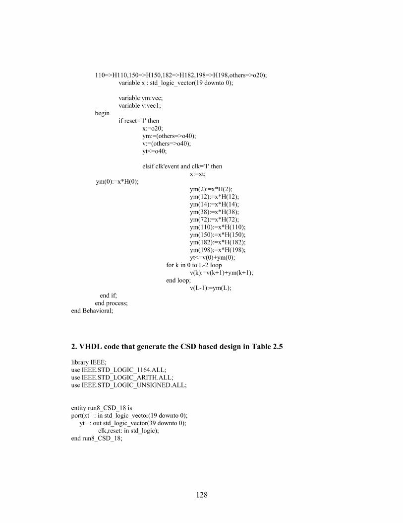
128
110=>H110,150=>H150,182=>H182,198=>H198,others=>o20); variable x : std_logic_vector(19 downto 0); variable ym:vec; variable v:vec1; begin if reset='1' then x:=o20; ym:=(others=>o40); v:=(others=>o40); yt<=o40; elsif clk'event and clk='1' then x:=xt; ym(0):=x*H(0); ym(2):=x*H(2); ym(12):=x*H(12); ym(14):=x*H(14); ym(38):=x*H(38); ym(72):=x*H(72); ym(110):=x*H(110); ym(150):=x*H(150); ym(182):=x*H(182); ym(198):=x*H(198); yt<=v(0)+ym(0); for k in 0 to L-2 loop v(k):=v(k+1)+ym(k+1); end loop; v(L-1):=ym(L); end if; end process; end Behavioral; 2. VHDL code that generate the CSD based design in Table 2.5 library IEEE; use IEEE.STD_LOGIC_1164.ALL; use IEEE.STD_LOGIC_ARITH.ALL; use IEEE.STD_LOGIC_UNSIGNED.ALL; entity run8_CSD_18 is port(xt : in std_logic_vector(19 downto 0); yt : out std_logic_vector(39 downto 0); clk,reset: in std_logic); end run8_CSD_18;
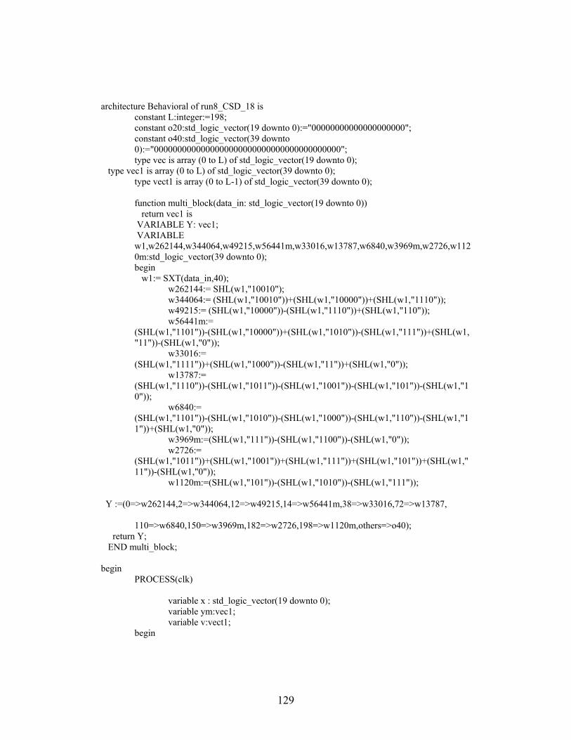
129
architecture Behavioral of run8_CSD_18 is constant L:integer:=198; constant o20:std_logic_vector(19 downto 0):="00000000000000000000"; constant o40:std_logic_vector(39 downto
0):="0000000000000000000000000000000000000000"; type vec is array (0 to L) of std_logic_vector(19 downto 0); type vec1 is array (0 to L) of std_logic_vector(39 downto 0); type vect1 is array (0 to L-1) of std_logic_vector(39 downto 0); function multi_block(data_in: std_logic_vector(19 downto 0)) return vec1 is VARIABLE Y: vec1; VARIABLE
w1,w262144,w344064,w49215,w56441m,w33016,w13787,w6840,w3969m,w2726,w1120m:std_logic_vector(39 downto 0);
begin w1:= SXT(data_in,40); w262144:= SHL(w1,"10010"); w344064:= (SHL(w1,"10010"))+(SHL(w1,"10000"))+(SHL(w1,"1110")); w49215:= (SHL(w1,"10000"))-(SHL(w1,"1110"))+(SHL(w1,"110")); w56441m:=
(SHL(w1,"1101"))-(SHL(w1,"10000"))+(SHL(w1,"1010"))-(SHL(w1,"111"))+(SHL(w1,"11"))-(SHL(w1,"0"));
w33016:= (SHL(w1,"1111"))+(SHL(w1,"1000"))-(SHL(w1,"11"))+(SHL(w1,"0"));
w13787:= (SHL(w1,"1110"))-(SHL(w1,"1011"))-(SHL(w1,"1001"))-(SHL(w1,"101"))-(SHL(w1,"10"));
w6840:= (SHL(w1,"1101"))-(SHL(w1,"1010"))-(SHL(w1,"1000"))-(SHL(w1,"110"))-(SHL(w1,"11"))+(SHL(w1,"0"));
w3969m:=(SHL(w1,"111"))-(SHL(w1,"1100"))-(SHL(w1,"0")); w2726:=
(SHL(w1,"1011"))+(SHL(w1,"1001"))+(SHL(w1,"111"))+(SHL(w1,"101"))+(SHL(w1,"11"))-(SHL(w1,"0"));
w1120m:=(SHL(w1,"101"))-(SHL(w1,"1010"))-(SHL(w1,"111")); Y :=(0=>w262144,2=>w344064,12=>w49215,14=>w56441m,38=>w33016,72=>w13787,
110=>w6840,150=>w3969m,182=>w2726,198=>w1120m,others=>o40); return Y; END multi_block; begin PROCESS(clk) variable x : std_logic_vector(19 downto 0); variable ym:vec1; variable v:vect1; begin
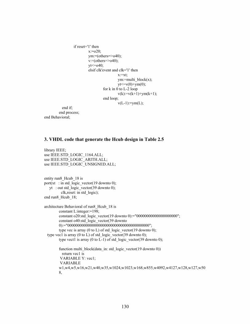
130
if reset='1' then x:=o20; ym:=(others=>o40); v:=(others=>o40); yt<=o40; elsif clk'event and clk='1' then x:=xt; ym:=multi_block(x); yt<=v(0)+ym(0); for k in 0 to L-2 loop v(k):=v(k+1)+ym(k+1); end loop; v(L-1):=ym(L); end if; end process; end Behavioral; 3. VHDL code that generate the Hcub design in Table 2.5 library IEEE; use IEEE.STD_LOGIC_1164.ALL; use IEEE.STD_LOGIC_ARITH.ALL; use IEEE.STD_LOGIC_UNSIGNED.ALL; entity run8_Hcub_18 is port(xt : in std_logic_vector(19 downto 0); yt : out std_logic_vector(39 downto 0); clk,reset: in std_logic); end run8_Hcub_18; architecture Behavioral of run8_Hcub_18 is constant L:integer:=198; constant o20:std_logic_vector(19 downto 0):="00000000000000000000"; constant o40:std_logic_vector(39 downto
0):="0000000000000000000000000000000000000000"; type vec is array (0 to L) of std_logic_vector(19 downto 0); type vec1 is array (0 to L) of std_logic_vector(39 downto 0); type vect1 is array (0 to L-1) of std_logic_vector(39 downto 0); function multi_block(data_in: std_logic_vector(19 downto 0)) return vec1 is VARIABLE Y: vec1; VARIABLE
w1,w4,w5,w16,w21,w40,w35,w1024,w1023,w168,w855,w4092,w4127,w128,w127,w508,
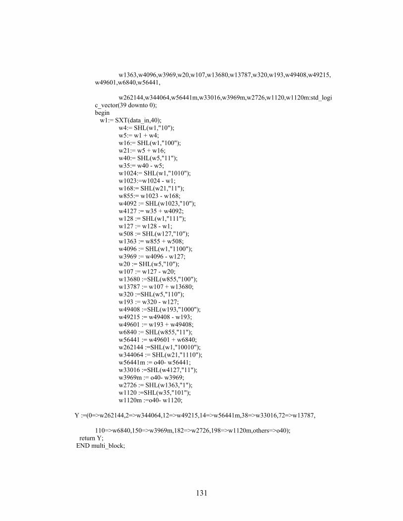
131
w1363,w4096,w3969,w20,w107,w13680,w13787,w320,w193,w49408,w49215,w49601,w6840,w56441,
w262144,w344064,w56441m,w33016,w3969m,w2726,w1120,w1120m:std_logic_vector(39 downto 0);
begin w1:= SXT(data_in,40); w4:= SHL(w1,"10"); w5:= w1 + w4; w16:= SHL(w1,"100"); w21:= w5 + w16; w40:= SHL(w5,"11"); w35:= w40 - w5; w1024:= SHL(w1,"1010"); w1023:=w1024 - w1; w168:= SHL(w21,"11"); w855:= w1023 - w168; w4092 := SHL(w1023,"10");
w4127 := w35 + w4092; w128 := SHL(w1,"111"); w127 := w128 - w1; w508 := SHL(w127,"10"); w1363 := w855 + w508; w4096 := SHL(w1,"1100"); w3969 := w4096 - w127; w20 := SHL(w5,"10"); w107 := w127 - w20; w13680 :=SHL(w855,"100"); w13787 := w107 + w13680; w320 :=SHL(w5,"110"); w193 := w320 - w127; w49408 :=SHL(w193,"1000"); w49215 := w49408 - w193; w49601 := w193 + w49408; w6840 := SHL(w855,"11"); w56441 := w49601 + w6840; w262144 :=SHL(w1,"10010"); w344064 := SHL(w21,"1110"); w56441m := o40- w56441; w33016 :=SHL(w4127,"11"); w3969m := o40- w3969; w2726 := SHL(w1363,"1"); w1120 :=SHL(w35,"101"); w1120m :=o40- w1120; Y :=(0=>w262144,2=>w344064,12=>w49215,14=>w56441m,38=>w33016,72=>w13787,
110=>w6840,150=>w3969m,182=>w2726,198=>w1120m,others=>o40); return Y; END multi_block;
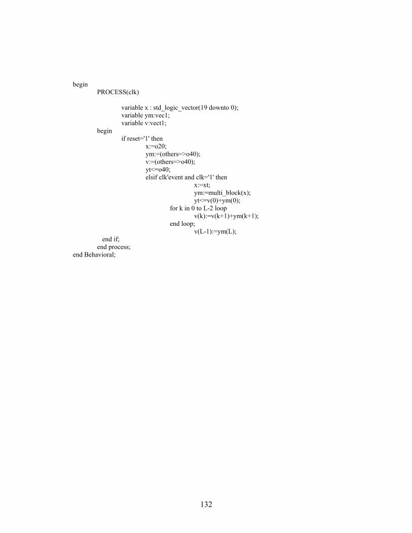
132
begin PROCESS(clk) variable x : std_logic_vector(19 downto 0); variable ym:vec1; variable v:vect1; begin if reset='1' then x:=o20; ym:=(others=>o40); v:=(others=>o40); yt<=o40; elsif clk'event and clk='1' then x:=xt; ym:=multi_block(x); yt<=v(0)+ym(0); for k in 0 to L-2 loop v(k):=v(k+1)+ym(k+1); end loop; v(L-1):=ym(L); end if; end process; end Behavioral;
Related Documents

![Unrorsity ]hten)âtLOiial - ShareOK](https://static.cupdf.com/doc/110x72/631b0c80c51d6b41aa0512b3/unrorsity-htenatloiial-shareok.jpg)