HCD-GP5 US Model Canadian Model AEP Model UK Model E Model Australian Model SERVICE MANUAL MICRO HI-FI COMPONENT SYSTEM Sony Corporation Personal Audio Company Published by Sony Engineering Corporation 9-877-380-06 2004J16-1 © 2004.10 HCD-GP5 is the Amplifier, CD player, Tape Deck and Tuner section in CMT-GP5. SPECIFICATIONS Ver 1.5 2004.10 Model Name Using Similar Mechanism NEW CD CD Mechanism Type CDM55A-K6BD44B Section Base Unit Name BU-K1BD44B Optical Pick-up Name KSM-213D TAPE Model Name Using Similar Mechanism NEW Section Tape Transport Mechanism Type CMAL1Z240A — Continued on next page — Amplifier section AUDIO POWER SPECIFICATIONS: (U.S.A. model only) POWER OUTPUT AND TOTAL HARMONIC DISTORTION: With 6-ohm loads, both channels driven, from 120 - 10,000 Hz; rated 35 watts per channel minimum RMS power, with no more than 10% total harmonic distortion from 250 milliwatts to rated output. North American model: Continuous RMS power output (reference): 35 + 35 W (6 ohms at 1 kHz, 10% THD) European model: DIN power output (rated): 30 + 30 W (6 ohms at 1 kHz, DIN) Continuous RMS power output (reference): 30 + 30 W (6 ohms at 1 kHz, 10% THD) Music power output (reference): 60 + 60 W Other models: The following measured at AC 230 V or AC 120 V, 50/ 60 Hz DIN power output (rated): 30 + 30 W (6 ohms at 1 kHz, DIN) Continuous RMS power output (reference): 30 + 30 W (6 ohms at 1 kHz, 10% THD) Inputs MD IN (phono jacks): Sensitivity 500 mV, impedance 47 kilohms Outputs PHONES (stereo minijack): Accepts headphones with an impedance of 8 ohms or more SPEAKERS: Accepts impedance of 6 to 16 ohms. CD player section System Compact disc and digital audio system Laser Semiconductor laser (λ=780 nm) Emission duration: continuous Frequency response 2 Hz – 20 kHz (±0.5 dB) Tape deck section Recording system 4-track 2-channel stereo Frequency response 50 – 13,000 Hz (±3 dB), using Sony TYPE I cassettes Tuner section FM stereo, FM/AM superheterodyne tuner FM tuner section Tuning range 87.5 – 108.0 MHz (50-kHz step) Antenna FM lead antenna Antenna terminals 75 ohms balanced Intermediate frequency 10.7 MHz AM tuner section Tuning range Pan-American model: 530 – 1,710 kHz (with the tuning interval set at 10 kHz) 531 – 1,710 kHz (with the tuning interval set at 9 kHz) European model: 531 – 1,602 kHz (with the tuning interval set at 9 kHz) Other models: 530 – 1,710 kHz (with the tuning interval set at 10 kHz) 531 – 1,602 kHz (with the tuning interval set at 9 kHz) Antenna AM loop antenna, external antenna terminal Intermediate frequency 450 kHz

Welcome message from author
This document is posted to help you gain knowledge. Please leave a comment to let me know what you think about it! Share it to your friends and learn new things together.
Transcript

HCD-GP5US Model
Canadian ModelAEP Model UK Model
E ModelAustralian Model
SERVICE MANUAL
MICRO HI-FI COMPONENT SYSTEMSony CorporationPersonal Audio Company
Published by Sony Engineering Corporation
9-877-380-062004J16-1
© 2004.10
HCD-GP5 is the Amplifier, CD player, TapeDeck and Tuner section in CMT-GP5.
SPECIFICATIONS
Ver 1.5 2004.10
Model Name Using Similar Mechanism NEW
CD CD Mechanism Type CDM55A-K6BD44B
Section Base Unit Name BU-K1BD44B
Optical Pick-up Name KSM-213D
TAPE Model Name Using Similar Mechanism NEW
Section Tape Transport Mechanism Type CMAL1Z240A
— Continued on next page —
Amplifier section
AUDIO POWER SPECIFICATIONS:(U.S.A. model only)POWER OUTPUT AND TOTAL HARMONIC DISTORTION:With 6-ohm loads, both channels driven, from 120 - 10,000 Hz; rated 35 watts per channel minimum RMS power, with no more than 10% total harmonic distortion from 250 milliwatts to rated output.North American model:Continuous RMS power output (reference):
35 + 35 W (6 ohms at 1 kHz, 10% THD)
European model:DIN power output (rated): 30 + 30 W
(6 ohms at 1 kHz, DIN)Continuous RMS power output (reference):
30 + 30 W (6 ohms at 1 kHz, 10% THD)
Music power output (reference):60 + 60 W
Other models: The following measured at AC 230 V or AC 120 V, 50/60 HzDIN power output (rated): 30 + 30 W
(6 ohms at 1 kHz, DIN)Continuous RMS power output (reference):
30 + 30 W (6 ohms at 1 kHz, 10% THD)
InputsMD IN (phono jacks):
Sensitivity 500 mV, impedance 47 kilohms
OutputsPHONES (stereo minijack):
Accepts headphones with an impedance of 8 ohms or more
SPEAKERS: Accepts impedance of 6 to 16 ohms.
CD player sectionSystem Compact disc and digital
audio systemLaser Semiconductor laser
(λ=780 nm)Emission duration: continuous
Frequency response 2 Hz – 20 kHz (±0.5 dB)
Tape deck sectionRecording system 4-track 2-channel stereoFrequency response 50 – 13,000 Hz (±3 dB),
using Sony TYPE I cassettes
Tuner sectionFM stereo, FM/AM superheterodyne tuner
FM tuner section
Tuning range 87.5 – 108.0 MHz (50-kHz step)
Antenna FM lead antennaAntenna terminals 75 ohms balancedIntermediate frequency 10.7 MHz
AM tuner sectionTuning rangePan-American model: 530 – 1,710 kHz
(with the tuning interval set at 10 kHz)531 – 1,710 kHz (with the tuning interval set at 9 kHz)
European model: 531 – 1,602 kHz (with the tuning interval set at 9 kHz)
Other models: 530 – 1,710 kHz (with the tuning interval set at 10 kHz)531 – 1,602 kHz (with the tuning interval set at 9 kHz)
Antenna AM loop antenna, external antenna terminal
Intermediate frequency 450 kHz

2
HCD-GP5
TABLE OF CONTENTS
1. SERVICING NOTES ······················································· 3
2. GENERAL ·········································································· 5
3. DISASSEMBLY3-1. Top Cabinet, Rear Panel ·················································· 73-2. Front Panel Assy ····························································· 83-3. CONTROL Board, Single Cassette Mechanism ············· 83-4. CD Mechanism Deck (CDM55A-K6BD44B) ················ 93-5. MAIN Board, TRANSFORMER Board ······················· 103-6. LOADING Board ·························································· 103-7. CD Board ······································································ 113-8. Tray (CDM55D) ··························································· 113-9. Optical Pick-up (KSM-213D), Holder (C213) ············· 12
4. MECHANICAL ADJUSTMENTS ····························· 13
5. ELECTRICAL ADJUSTMENTS ······························· 14
6. DIAGRAMS ······································································ 176-1. Block Diagram ······························································ 196-2. Printed Wiring Board – CD Section – ························· 206-3. Schematic Diagram – CD Section – ···························· 216-4. Printed Wiring Board – Control Section – ··················· 226-5. Schematic Diagram – Control Section – ······················ 236-6. Printed Wiring Boards – Main Section – ····················· 246-7. Schematic Diagram – Main Section (1/4) – ················· 256-8. Schematic Diagram – Main Section (2/4) – ················· 266-9. Schematic Diagram – Main Section (3/4) – ················· 276-10. Schematic Diagram – Main Section (4/4) – ··············· 286-11. Printed Wiring Board – Power Section – ··················· 296-12. Schematic Diagram – Power Section – ······················ 306-13. IC Pin Function Description ······································· 35
7. EXPLODED VIEWS7-1. Overall Section ····························································· 377-2. Front Panel Section ······················································· 387-3. Chassis Section ····························································· 397-4. CD Mechanism Deck Setion ········································· 407-5. KSM-213D···································································· 41
8. ELECTRICAL PARTS LIST ······································· 42
SAFETY-RELATED COMPONENT WARNING!!
COMPONENTS IDENTIFIED BY MARK 0 OR DOTTED LINE WITHMARK 0 ON THE SCHEMATIC DIAGRAMS AND IN THE PARTSLIST ARE CRITICAL TO SAFE OPERATION. REPLACE THESECOMPONENTS WITH SONY PARTS WHOSE PART NUMBERSAPPEAR AS SHOWN IN THIS MANUAL OR IN SUPPLEMENTSPUBLISHED BY SONY.
ATTENTION AU COMPOSANT AYANT RAPPORTÀ LA SÉCURITÉ!
LES COMPOSANTS IDENTIFÉS PAR UNE MARQUE 0 SUR LESDIAGRAMMES SCHÉMATIQUES ET LA LISTE DES PIÈCES SONTCRITIQUES POUR LA SÉCURITÉ DE FONCTIONNEMENT. NEREMPLACER CES COMPOSANTS QUE PAR DES PIÈSES SONYDONT LES NUMÉROS SONT DONNÉS DANS CE MANUEL OUDANS LES SUPPÉMENTS PUBLIÉS PAR SONY.
Ver 1.3 2004.01
GeneralPower requirementsNorth American model: 120 V AC, 60 HzEuropean model: 230 V AC, 50/60 Hz
Other models:
Power consumptionNorth American model: 60 wattsEuropean model: 60 watts
0.3 watts (in the standby mode)
Other models: 60 wattsDimensions (w/h/d) Approx. 190 × 250 × 270
mmMass Approx. 4.6 kg
Design and specifications are subject to change without notice.
Australian model: 230 - 240 V AC, 50/60 HzHong Kong model: 220 - 240 V AC, 50/60 HzSingaporean model: 220 - 240 V AC, 50/60 Hz
110 - 120 V or 220 - 240 VAC, 50/60 HzAdjustable with voltageselector

3
HCD-GP5SECTION 1
SERVICING NOTES
Fig. A. Using an AC voltmeter to check AC leakage.
1.5 kΩ0.15 µFACvoltmeter(0.75 V)
To Exposed MetalParts on Set
Earth Ground
SAFETY CHECK-OUTAfter correcting the original service problem, perform the followingsafety check before releasing the set to the customer:Check the antenna terminals, metal trim, “metallized” knobs, screws,and all other exposed metal parts for AC leakage.Check leakage as described below.
LEAKAGE TESTThe AC leakage from any exposed metal part to earth ground andfrom all exposed metal parts to any exposed metal part having areturn to chassis, must not exceed 0.5 mA (500 microamperes.).Leakage current can be measured by any one of three methods.1. A commercial leakage tester, such as the Simpson 229 or RCA
WT-540A. Follow the manufacturers’ instructions to use theseinstruments.
2. A battery-operated AC milliammeter. The Data Precision 245digital multimeter is suitable for this job.
3. Measuring the voltage drop across a resistor by means of a VOMor battery-operated AC voltmeter. The “limit” indication is 0.75V, so analog meters must have an accurate low-voltage scale.The Simpson 250 and Sanwa SH-63Trd are examples of apassive VOM that is suitable. Nearly all battery operated digitalmultimeters that have a 2 V AC range are suitable. (See Fig. A)
CAUTIONUse of controls or adjustments or performance of proceduresother than those specified herein may result in hazardousradiation exposure.
This appliance is classified as a CLASS 1 LASER product.The CLASS 1 LASER PRODUCT MARKING is located onthe exterior.
Laser component in this product is capable of emitting radiationexceeding the limit for Class 1.
The laser diode in the optical pick-up block may suffer electrostaticbreak-down because of the potential difference generated by thecharged electrostatic load, etc. on clothing and the human body.During repair, pay attention to electrostatic break-down and alsouse the procedure in the printed matter which is included in therepair parts.The flexible board is easily damaged and should be handled withcare.
NOTES ON LASER DIODE EMISSION CHECKThe laser beam on this model is concentrated so as to be focused onthe disc reflective surface by the objective lens in the optical pick-up block. Therefore, when checking the laser diode emission,observe from more than 30 cm away from the objective lens.
LASER DIODE AND FOCUS SEARCH OPERATIONCHECKCarry out the “S curve check” in “CD section adjustment” and checkthat the S curve waveforms is output three times.
NOTES ON HANDLING THE OPTICAL PICK-UPBLOCK OR BASE UNIT
Notes on chip component replacement• Never reuse a disconnected chip component.• Notice that the minus side of a tantalum capacitor may be dam-
aged by heat.
Flexible Circuit Board Repairing• Keep the temperature of the soldering iron around 270 ˚C during
repairing.• Do not touch the soldering iron on the same conductor of the
circuit board (within 3 times).• Be careful not to apply force on the conductor when soldering or
unsoldering.
4
HCD-GP5
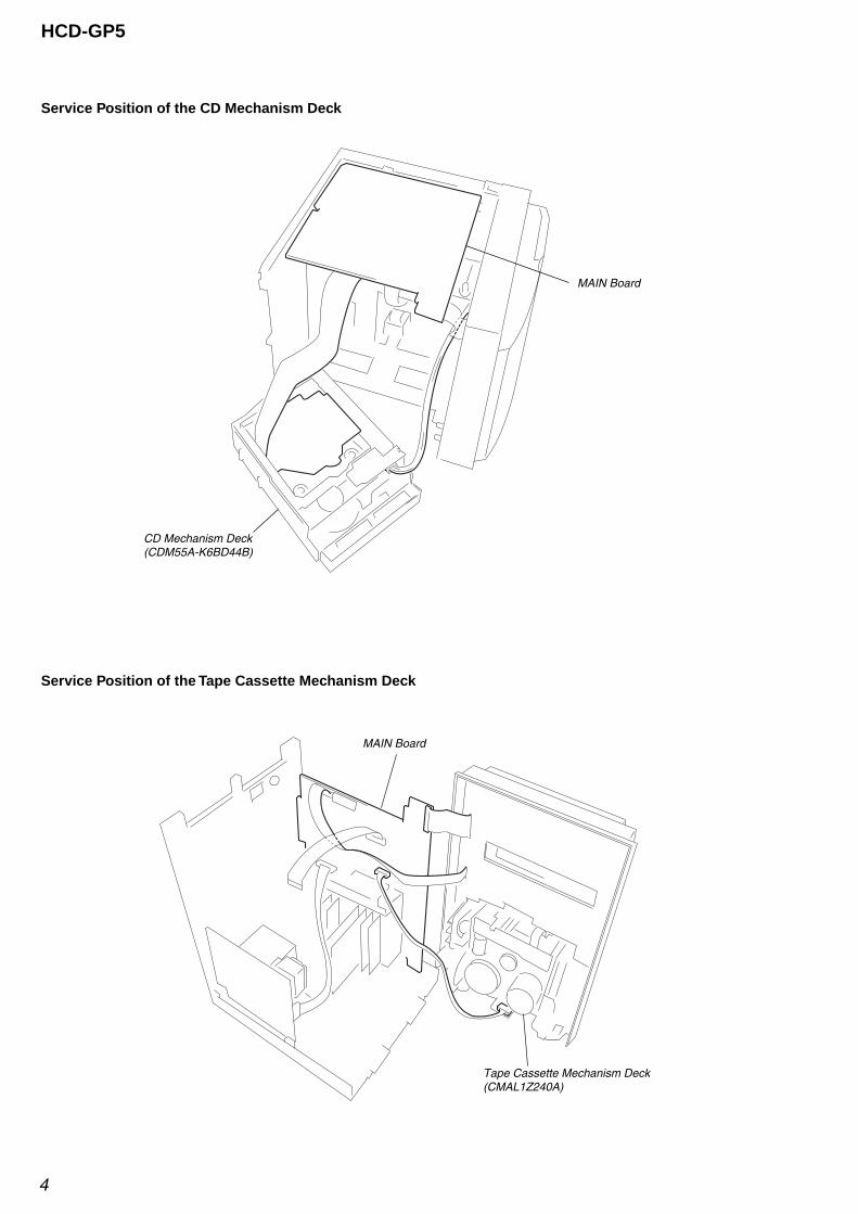
Service Position of the CD Mechanism Deck
Service Position of the Tape Cassette Mechanism Deck
MAIN Board
CD Mechanism Deck(CDM55A-K6BD44B)
MAIN Board
Tape Cassette Mechanism Deck (CMAL1Z240A)
5
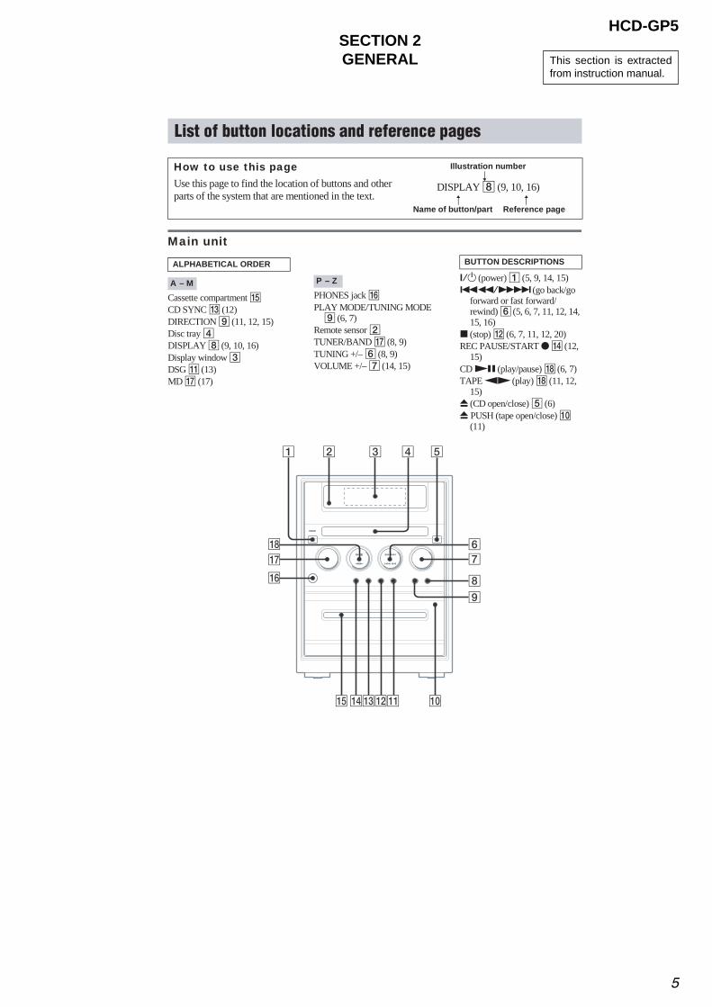
HCD-GP5SECTION 2GENERAL This section is extracted
from instruction manual.
Main unit
Cassette compartment qgCD SYNC qd (12)DIRECTION 9 (11, 12, 15)Disc tray 4DISPLAY 8 (9, 10, 16)Display window 3DSG qa (13)MD qj (17)
PHONES jack qhPLAY MODE/TUNING MODE 9 (6, 7)
Remote sensor 2TUNER/BAND qj (8, 9)TUNING +/– 6 (8, 9)VOLUME +/– 7 (14, 15)
?/1 (power) 1 (5, 9, 14, 15).m/M> (go back/go
forward or fast forward/rewind) 6 (5, 6, 7, 11, 12, 14, 15, 16)
x (stop) qs (6, 7, 11, 12, 20)REC PAUSE/START z qf (12,
15)CD NX (play/pause) qk (6, 7)TAPE nN (play) qk (11, 12,
15)Z (CD open/close) 5 (6)Z PUSH (tape open/close) 0
(11)
List of button locations and reference pages
How to use this pageUse this page to find the location of buttons and other parts of the system that are mentioned in the text.
Illustration numberr
DISPLAY 8 (9, 10, 16)R R
Name of button/part Reference page
ALPHABETICAL ORDER
A – M P – Z
BUTTON DESCRIPTIONS
1 2 3 4 5
6
7
8
qk
qj
qh
9
0qaqsqdqfqg

6
HCD-GP5
Remote control
BASS +/– 0 (13)CLEAR 8 (8, 9)CLOCK/TIMER SELECT w;
(14, 15)CLOCK/TIMER SET wa (5, 14,
15)DISPLAY 2 (9, 10, 16) DSG qa (13)MD qk (17)
PLAY MODE/DIRECTION qd (6, 7, 11, 12, 15)
PRESET +/– 5 (9) REPEAT/FM MODE qf (7, 9)SLEEP ql (13)TREBLE +/– 9 (13)TUNER BAND qh (8, 9)TUNER MEMORY qs (8)TUNING +/– 6 (8, 9)VOL +/– 7 (14, 15)
?/1 (power) 1 (5, 9, 14, 15)m/M (fast forward/rewind) 6 (6, 11)
./> (go back/go forward) 5 (5, 6, 7, 12, 14, 15, 16)
x (stop) 4 (6, 7, 11, 12, 20)X (pause) 3 (6, 11)CD N (play) qj (6, 7)TAPE nN (play) qg (11, 12,
15)
ALPHABETICAL ORDER
A – M P – Z
BUTTON DESCRIPTIONS
1
waw;qlqk
qj
qh
qg
qf
qd
qs
qa
2
34
5
6
7
8
9
0
Use buttons on the remote for the operation.
1 Press ?/1 to turn on the system.
2 Press CLOCK/TIMER SET.
3 Press ./> repeatedly to set the hour.
4 Press CLOCK/TIMER SET.
5 Press ./> repeatedly to set the minute.
6 Press CLOCK/TIMER SET.
The clock starts working.
To adjust the clock
1 Press CLOCK/TIMER SET.
2 Press ./> to select “CLOCK”, then press CLOCK/TIMER SET.
3 Do the same procedures as step 3 to 6 above.
Setting the clock

7
HCD-GP5SECTION 3
DISASSEMBLY
Note: Follow the disassembly procedure in the numerical order given.
• This set can be disassembled in the order shown below.
3-1. Top Cabinet, Rear Panel
MAIN BOARD,TRANSFORMER BOARD
LOADING BOARD CD BOARD TRAY (CDM55D)
OPTICAL PICK-UP(KSM-213D),HOLDER (C213)
CD MECHANISM DECK(CDM55A-K6BD44B)
CONTROL BOARD,SINGLE CASSETTE MECHANISM
FRONT PANEL ASSY
SET
TOP CABINET,REAR PANEL
4
a
a
b
b
5 top cabinet
1 three screws (+KTP 3 ×12)
2 three screws (+KTP 3 ×12)
3 six screws (+BVTP 3 ×10)
6wire (flat type) 11p
q; tuner (FM/AM)
CN304
7 two screws (+BVTP 3 ×10)
9 three screws (+BVTP 3 ×10)
8 three screws (+BVTP 3 ×10)
qa rear panel
Ver 1.2 2003.11

8
HCD-GP5
3-2. Front Panel Assy
3-3. CONTROL Board, Single Cassette Mechanism
5 wire (flat type) 13p (CN303)
4 four screws (+BVTP 3 ×10)
3 two screws (+KTP 3 ×12)
6 wire (flat type) 26p (CN302)
q; front panel assy
7 connector 5p (CN1)
1 four claws
2 CD lid
9 connector 5p (CN201)
8 connector 6p
q; single cassette mechanism(CMAL1Z240A)
7 CONTROL board
1 three screws (+BVTP 3 × 10)
2 four screws (+BVTP 3 × 10)
3 four screws (+BVTP 3 × 10)
8 four screws(+BVTP 3 × 10)
4 wire (flat type) 26p (CN601)
5 wire (flat type) 13p (CN602)
6 wire (flat type) 8p (CN603)
9 two clamp

9
HCD-GP5
3-4. CD Mechanism Deck (CDM55A-K6BD44B)
5
2 screw (+BVTP 3 ×10)
CN305
4 screw (+BVTP 3 ×10)
1 CD plate
6 CD holder
3 wire (flat type) 21p (CN101,305)
7 CD mechanism deck (CDM55A-K6BD44B)
CN101

10
HCD-GP5
3-5. MAIN Board, TRANSFORMER Board
3-6. LOADING Board
5 LOADING board
2 two screws (+BTP 2.6 × 6)
4 motor (LD) assy (M901)
1 Remove the belt.
3 Remove soldering from the two points.
1 connector 9p (CN801)
5 main heat sink
8 sub heat sink
9 MAIN board
2 two screws (+BVTP 3 ×10)
7 two screws (+BVTP 3 ×10)
6 two screws (+BVTP 3 ×10)
4 two screws (+BVTP 3 ×10)
3 three screws (+BVTP 3 ×10)
q; four screws (+BVTP 3 ×10)
qs TRANSFORMER board
qa power transformer
11
HCD-GP5
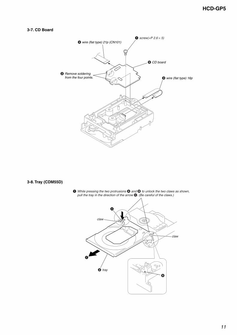
2 Remove soldering from the four points. 3 wire (flat type) 16p
5 CD board
4 wire (flat type) 21p (CN101)1 screw(+P 2.6 × 5)
2 tray
1 While pressing the two protrusions A and B to unlock the two claws as shown, pull the tray in the direction of the arrow C. (Be careful of the claws.)
claw
claw
C
A
B
3-7. CD Board
3-8. Tray (CDM55D)

12
HCD-GP5
3-9. Optical Pick-up (KSM-213D), Holder (C213)
1 two floating screws (+PTPWH M2.6)
qf floating screws (+PTPWH M2.6)
qg holder (C213)
5 screw (+PTTP M2.6)
6 stopper (BU)
2 two compression spring (T213)
7 compression spring (T213)
3 insulator
8 insulator 9 screw (+PTTP M2.6)
q; stopper (BU)
qa compression spring (T213)
qs insulator
qd optical pick-up (KSM-213D)
4 insulator
Ver 1.2 2003.11

13
HCD-GP5SECTION 4
MECHANICAL ADJUSTMENTS
3.04 – 6.96 mN • m(31 to 71 g • cm)
(0.43 – 0.98 oz • inch)0.20 – 0.58 mN • m
(2 to 6 g • cm)(0.02 – 0.08 oz • inch)
3.04 – 6.96 mN • m(31 to 71 g • cm)
(0.43 – 0.98 oz • inch)0.20 – 0.58 mN • m
(2 to 6 g • cm)(0.02 – 0.08 oz • inch)6.97 – 14.02 mN • m
(71 to 143 g • cm)(0.98 – 1.99 oz • inch)9.8 mN • m or more(100 g • cm or more)
(1.4 oz • inch or more)9.8 mN • m or more(100 g • cm or more)
(1.4 oz • inch or more)
CQ-102C
CQ-102C
CQ-102RC
CQ-102RC
CQ-201B
CQ-403A
CQ-403R
Precaution1. Clean the following parts with a denatured alcohol-moistened
swab:record/playback heads pinch rollerserase head rubber beltscapstan idlers
2. Demagnetize the record/playback head with a head demag-netizer.
3. Do not use a magnetized screwdriver for the adjustments.4. After the adjustments, apply suitable locking compound to the
parts adjusted.5. The adjustments should be performed with the rated power
supply voltage unless otherwise noted.
Torque Measurement
Mode
FWD
FWDback tension
REV
REVback tension
FF/REW
FWD tension
REV tension
Torque meter Meter reading

14
HCD-GP5SECTION 5
ELECTRICAL ADJUSTMENTS
[Record/Playback Head Azimuth Adjustment]Procedure:1. Mode : Playback
2. Turn the adjustment screw and check output peaks. If the peaksdo not match for L-CH and R-CH, turn the adjustment screwso that outputs match within 1 dB of peak.
test tapeP-4-A100(10kHz, –10dB) MAIN board
J203speaker terminal
level meter
set +
–
L-CHpeak
R-CHpeak
screwposition
outputlevel within
1 dB
L-CHpeak
R-CHpeak
screwposition
within 1dB
Signal Used forTape
P-4-A100
WS-48B
10 kHz, –10 dB
3 kHz, 0 dB
Azimuth Adjustment
Tape Speed Adjustment
DECK SECTION 0 dB=0.775V
1. Demagnetize the record/playback head with a head demagnetizer.2. Do not use a magnetized screwdriver for the adjustments.3. After the adjustments, apply suitable locking compound to the
parts adjusted.4. The adjustments should be performed with the rated power
supply voltage unless otherwise noted.5. The adjustments should be performed in the order given in this
service manual. (As a general rule, playback circuit adjustmentshould be completed before performing recording circuitadjustment.)
6. The adjustments should be performed for both L-CH and R-CH.
7. Switches and controls should be set as follows unless otherwisespecified.
4. After the adjustments, apply suitable locking compound to theparts adjusted.
Adjustment Location: Record/Playback/Erase Head
[Tape Speed Check]Procedure:1. Turn the power on.2. Insert the WS-48B into deck.3. Press the Y button of deck.4. Check the reading of frequency counter becomes 3000 ± 90 Hz.
Sample Value of Wow and flutterW.RMS (JIS) less than 0.3%(test tape: WS-48B)
3. Mode: Playback
test tapeP-4-A100(10kHz, –10dB)
oscilloscope
set
Waveform of oscilloscope
in phase 45° 90° 135° 180°
good wrong
MAIN boardJ203speaker terminal
L
R

15
HCD-GP5
RFDC signal waveform
Checking Location: CD board (Conductor side)
RFAC Level CheckConnection:
Procedure:1. Connect an oscilloscope to test point TP (RFAC) and TP (VC)
on the CD board.2. Turn the power on.3. Put the disc (YEDS-18) in to playback the number five track.4. Confirm that oscilloscope waveform is clear and check RFAC
signal level is correct or not.Note: A clear RFAC signal waveform means that the shape “◊” can be
clearly distinguished at the center of the waveform.
RFAC signal waveform
Checking Location: CD board (Conductor side)
CD SECTION
Note:1. CD Block is basically designed to operate without adjustment. There-
fore, check each item in order given.2. Use YEDS-18 disc (3-702-101-01) unless otherwise indicated.3. Use an oscilloscope with more than 10MΩ impedance.4. Clean the object lens by an applicator with neutral detergent when the
signal level is low than specified value with the following checks.
S-curve CheckConnection:
Procedure:1. Connect an oscilloscope to test point TP (FE) and TP (DVC)
on the CD board.2. Turn the power on.3. Put the disc (YEDS-18) in and turned power switch on again
and actuate the focus search. (actuate the focus search whendisc table is moving in and out)
4. Check the oscilloscope waveform (S-curve) is symmetricalbetween A and B. And confirm peak to peak level within 2 ± 1Vp-p.
S-curve waveform
Note: • Try to measure several times to make sure than the ratio of A : Bor B : A is more than 10 : 7.
• Take sweep time as long as possible and light up thebrightness to obtain best waveform.
Checking Location: CD board (Conductor side)
RFDC Level CheckConnection:
Procedure:1. Connect an oscilloscope to test point TP (RFDC) and TP (DVC)
on the CD board.2. Turn the power on.3. Put the disc (YEDS-18) in to playback the number five track.4. Confirm that oscilloscope waveform is clear and check RFDC
signal level is correct or not.Note: A clear RFDC signal waveform means that the shape “◊” can be
clearly distinguished at the center of the waveform.
+–
CD board
TP (FE)TP (DVC)
oscilloscope
A
B
symmetry
within 2 ± 1 Vp-p
+–
CD board
TP (RFDC)TP (DVC)
oscilloscope
VOLT/DIV: 200 mVTIME/DIV: 500 ns
level: 0.7 ± 0.2 Vp-p
+–
CD board
TP (RFAC)TP (VC)
oscilloscope
VOLT/DIV: 200 mVTIME/DIV: 500 ns
level: 0.9 ± 0.4 Vp-p

16
HCD-GP5
E-F Balance CheckConnection:
Procedure:1. Connect an oscilloscpe to test point TP (TE) and TP (DVC) on
the CD board.2. AC is put in pushing CD u button.3. FL tube carries out all lights and goes into CD test mode.4. Put the disc (YEDS-18) in to playback the number five track.5. Press the CD u button. (The tracking servo and the sledding
servo are turned OFF)6. Check the level B of the oscilliscope's waveform and the A
(DC voltage) of the center of the Traverse waveform.Confirm the following :A/B x 100 = less than ± 22%
Traverse Waveform
7. Press the CD u button. (The tracking servo and sleddingservo are turned ON)Confirm the C (DC voltage) is almost equal to the A (DCvoltage) is step 4.
8. To exit from this mode, turn the power off.Notes: • Always move the optical pick-up to most inside track when
exiting from this mode. Otherwise, a disc will not be unloaded.• Do not run the sled motor excessively, otherwise the gear can
be chipped.
Traverse Waveform
Checking Location: CD board (Conductor side)
+–
CD board
TP (TE)TP (DVC)
oscilloscope
0V
B
level: 1.15 ± 0.5 Vp-p
Center of the waveform
A (DC voltage)
0V
Tracking servoSled servo
ON
C (DC voltage)
Tracking servoSled servo
OFF
Checking Location:
– CD BOARD (Conductor Side) –
TP (VC)
TP (FE)
TP (TE)TP
(RFDC)
TP (DVC)TP
(RFAC)
IC103
IC101

17
HCD-GP5SECTION 6DIAGRAMS
• Circuit Boards Location
THIS NOTE IS COMMON FOR PRINTED WIRING BOARDS AND SCHEMATIC DIAGRAMS.(In addition to this, the necessary note is printed in each block.)
For printed wiring boards.Note:• X : parts extracted from the component side.• Y : parts extracted from the conductor side.• f : internal component.• : Pattern from the side which enables seeing.
• A : B+ Line.• B : B– Line.• Voltages are taken with a VOM (Input impedance 10 MΩ).
Voltage variations may be noted due to normal produc-tion tolerances.
• Waveforms are taken with a oscilloscope.Voltage variations may be noted due to normal produc-tion tolerances.
• Circled numbers refer to waveforms.• Signal path.
F : TUNERJ : CDd : MDE : PB (TAPE)a : REC (TAPE)
• AbbreviationAUS : Australian modelCND : Canadian modelE51 : Chilean and Peruvian modelsHK : Hong Kong modelKR : Korean modelSP : Singapore modelTW : Taiwan model
• Indication of transistor
Note:The components identified bymark 0 or dotted line with mark0 are critical for safety.Replace only with part numberspecified.
Note:Les composants identifiés parune marque 0 sont critiquespour la sécurité.Ne les remplacer que par unepièce portant le numéro spécifié.
MAIN board
CD boardLOADING board
TRANSFORMER board
CONTROL board
HEADPHONE board
C
B
These are omitted.
E
Q
B
These are omitted.
C E
B
These are omitted.
C E
Ver 1.3 2004.01
For schematic diagrams.Note:• All capacitors are in µF unless otherwise noted. pF: µµF
50 WV or less are not indicated except for electrolyticsand tantalums.
• All resistors are in Ω and 1/4 W or less unless otherwise
specified.• f : internal component.• 2 : nonflammable resistor.• 1 : fusible resistor.• C : panel designation.

18
HCD-GP5
• Waveforms– CD Board –
1.1Vp-p
1 IC103 qg (RFAC)(CD Play Mode)
2 IC101 el (FE)(CD Play Mode)
200mV/DIV, 1 µs/DIV
50mV/DIV, 200 µs/DIV
100mV/DIV, 200 µs/DIV
1V/DIV, 20ns/DIV
200mVp-p
250mVp-p
3 IC101 ra (TE)(CD Play Mode)
4 IC101 yj (XTAO)
5.4Vp-p59ns
6 IC601 qh (XOUT)
2V/DIV, 10 µs/DIV
5 IC601 qd (O-XT2)
5.4Vp-p30.5 µs
1V/DIV, 40ns/DIV
2.7Vp-p116ns
7 Q301 collector (Rec mode)
5V/DIV, 5 µs/DIV
10.6Vp-p10.9 µs
– CONTROL Board – – MAIN Board –

1919
HCD-GP5
6-1. Block Diagram
: TUNER
: CD
• Signal Path
• RCH is omitted due to same as L-CH.
: MD
: PB (TAPE)
: REC (TAPE)
R-CH
+VM
ERASEHEAD
REC/PBHEAD
DECK BLOCK
REC/PBSWITCH
R DATA98
R CLK100
R CE84
µ CONIC601
R COUNT99
L
RMD
J201
MUTE CONTQ506
J202PHONES
L
R
FUCTIONKEY
REMOTECONTROLRECEIVER
IC603
S601-607,612
TUNER UNIT
L-CH
R-CH R-CH
D OUT
D IN
CLK
CE
TUNED
R-CH
R TUNED93
Q305-311
L301BIAS
Q303,304
DECK BLOCK
MOTORDRIVE
Q606
T REC77
I XT112
O XT213
X60132.768kHz
X IN15
X OUT16
X6028.64MHz
MUTEQ504
76O DSG Q312
29RMC IN
FUCTIONKEY
S608-611S613-616
19I KEY2
31
RESETSWITCH
Q601
11I RESET RESET
IC602
21
26POWER DOWN
D801-804
RELAYDRIVE
ACIN
PT802SUB TRANS
Q401 RY801
18I KEY1
REG+10V +VM
PB/REC EQ AMPIC301
AUX L19 18OUT L
TU L23
TAPE L2
CD L2116OUT R R-CH
13CONT
28REC OUT
R MUTE80R STEREO92STEREO
MUTE
R-CH
M1DECK
MOTOR
T PLAY SW79
C DATA87
POWER AMPIC201
J203SPEAKER
SEG1
SEG20
34
44GRID1
GRID11
FLUORESCENTDISPLAY
FL601
+5VREG
Q602-604
µCON +B
VMD608
LINEFILTER
L801V ECO
PT801POWERTRANS
M
SW1PLAY
SW2R REC
BIASOSCQ301Q302
O PW M3E83
T END5
C CLK97
C XLT86
C SQSD96
C SCOR3
C SENS94
C XRST85
T SOL4
82CD ON
75LED CONT
LED601ECO LED
D605
D603
9P AMP MUTE
8P CONT
4L OUT
STBY10
L IN12
3R OUT
+VM
D422
D405
8POWER CONT
+5V
Q314-316
RDS SIG
RDS DATA
RDS CLK
SW3F REC
SW4PACK
SW5END
T SOLDRIVE
Q605
Q607
C LDON95
C PWM11
C PWM22
T MTR CONT6
T SW24
O SHIFT7
O BIAS 81
RDS SIG23
RDS CLK27RDS DATA91
F DATA10
PWRCONT
Q503
5+PRE
2+VCC
1-VCC
Q501,502
+VH
ACDET
Q508
DCDET
Q509,510
D434 D435+7V
D502+VM
25P MONI HOLDQ507
OVER LOADDET
J204SUBWOOFER
45
47
50
.
52
66
.
FIL1 FIL2
D609
FIL1
FIL2
D403
D402
D413
D427
D409
D410
+VMREG
Q402,403,405
+VCCREG
Q407
+VCC
CD P CONTQ415,417,418
+7VREG
Q416P CONT
Q406
+7V
+5VREG
Q419
D418D436
CD +5V
-VFLREG
Q413
-VFL
-VL
+VL
D423
D406
D404
+VH
-VH
DCDET
Q410D431
+VL
+VHREG
Q408,409
D425
DCDET
Q411D432
-VL
-VHREG
Q404
D416
D417-VP
+VP
D407
OUT1
OUT2
M
VM
RIN
FIN
CD DOORMOTOR UNIT
OPEN
CLOSEMOTOR DRIVEIC604
TRAYMOTOR
+VM (7V)
4
2
5
9
774O OPEN
73O CLOSE
28CD DOOR SW
OPTICAL PICK-UPBLOCK
(KSM-213D)
A
B
C
D
E
F
LD
VC
+5V
GND
PD
VR
LDDRIVE
FOCUSCOIL
TRACKINGCOIL
Q101
RF AMPIC103
VC27
A6B7C8D9E10F11
LD1
PD2
MOTOR/COIL DRIVEIC102
CH1RO13
CH1FO14
CH2RO11
CH2FO12
CH3RO18
CH3FO17
MSLEDMOTOR
CH4RO16
CH4FO15
MSPINDLEMOTOR
F+
F-
T-
T+
3CH1RI
2CH1FI
6CH2RI
5CH2FI
23CH3RI
24CH3FI
25CH4INS
20MUTE
MDP26
SFDR28
SRDR29
TRDR31
TFDR30
FRDR33
FFDR32
DIGITAL SERVOIC101
RFDC43
17FEI
28RFDCO
16FE
18TE
29RFDCI
12SW
FE39TE41SE40
72L OUT
75R OUT
5DATA
R-CH
7CLOK
6XLAT
2SQCK
9SCLK
20SCOR
1SQSO
27SSTP
66XTAI
67XTAO
3XRST
S101LIMIT
X10116.9344MHz
8SENS
RFAC5115RFAC
+3.3VREG
Q102,D101
+3.3V +5.5V
C SQCK88
STANDBY
Ver 1.2 2003.11

2020
HCD-GP5
6-2. Printed Wiring Board – CD Section –
IC102
IC101
IC103
TP (VC)
TP (RFAC)
TP (DVC)
CN30524
1-680-849-
D
1 2
A
B
C
D
E
F
G
3 4 5 6 7 8
Ref. No. Location
D101 F-5
IC101 E-4IC102 C-5IC103 D-2
Q101 C-2Q102 G-5
• SemiconductorLocation
• See page 17 for Circuit Boards Location.
Ver 1.2 2003.11

2121
HCD-GP5
6-3. Schematic Diagram – CD Section –
KSM-213D
(1/4)CN305
0uH
0uH
25
• See page 18 for Waveforms. • See page 31, 32 for IC Block Diagrams.
Ver 1.2 2003.11

2222
HCD-GP5
6-4. Printed Wiring Board – Control Section – • See page 17 for Circuit Boards Location.
IC601
IC60
2
IC603
IC604
US,CND,AEP,UK,KR
E51,HK,SP,TW,AUS
CONTROL BOARD
?/1
TUNER/BAND
CDNX
+M >
. m–
TAPEbB
zRECPAUSE/START
MD
VOL +
DISPLAY
Z
VOL –
PLAY MODE/TUNING MODE DSG
CD SYNC
x
1-689-573-
LOADING BOARD1
2
43
TOMAIN
BOARDCN302
(Page 24)
C
TOMAIN
BOARDCN303
(Page 24)
BTAPE
MECHANISMDECK
M901 1-674-336-
(12)12
FLUORESCENT INDICATOR TUBE
STANDBY
Ver 1.3 2004.01
Ref. No. Location
D601 A-2D602 B-5D603 B-6D604 B-5D605 A-1D606 D-5D607 B-5D608 B-5D609 B-5
IC601 A-3IC602 B-5IC603 B-6IC604 D-7
Q601 B-4Q602 A-2Q603 A-2Q604 A-2Q605 D-5Q606 D-5Q607 E-6Q608 B-6
• SemiconductorLocation

2323
HCD-GP5
6-5. Schematic Diagram – Control Section –
IC601VOLTAGE CHART
PIN NO. PIN NO. PIN NO.VOLT. VOLT. VOLT.
1 2.3 41 -31.0 81 0.5
2 2.3 42 -31.0 82 5.2
3 0 43 -31.0 83 0.4
4 0.8 44 -31.0 84 0
5 5.3 45 -31.0 85 5.2
6 10.2 46 5.2 86 5.2
7 0 47 -31.0 87 5.2
8 5.1 48 -31.0 88 5.2
9 0 49 -31.0 89 0
10 0 50 -31.0 90 5.2
11 5.1 51 0 91 0.2
12 0 52 -31.0 92 5.3
13 2.6 53 -31.0 93 5.3
14 0 54 -31.0 94 3.3
15 2.6 55 -31.0 95 0
16 2.6 56 -31.0 96 3.3
17 5.2 57 -31.0 97 5.2
18 5.3 58 -31.0 98 0
19 5.3 59 -31.0 99 0.7
20 0.1 60 -31.0 100 0
21 0.1 61 -31.0
22 0.1 62 -31.0
23 0.1 63 -31.0
24 2.0 64 -31.0
25 3.1 65 -31.0
26 5.6 66 -31.027 0.1 67 -
28 0 68 -29 5.3 69 2.5
30 - 70 5.0
31 - 71 0
32 - 72 5.2
33 - 73 5.2
34 -31.0 74 5.2
35 -31.0 75 0
36 -31.0 76 5.2
37 -31.0 77 0
38 -31.3 78 0
39 -31.0 79 4.9
40 -31.0 80 5.2
5.3 5.3
0
0
5.3
4.7
0
0
10.2
10.2
4.0
5.10
5.65.6
9.5(10.2)
10.2(10.2)
10.2(0.9)
10.1(1.0)
10.2(10.2)
0
2.0
9.5
8.8
5.9
2.5
8.2
1.9 2.50.5
RPM7140-V4
FLUORESCENT INDICATOR TUBE
100K
T-72
0T-721SS133
LC876764C-51E5
270
2SA1981Y
270
SLR-342VCT31
33P
1SS
133T
-72
2SC
2712
L-T
E85
R1SS133T-72
1N4148A-T265
1N4148A-T265
1SS133T-77
1SS133T-72
2SA1296GR-(TYPE2)
TU
NE
R/B
AN
D
MD
TAP
EY
x
z
RE
CPA
US
E/S
TAR
T
. m -
M >+
Z
uCDI/1
CONTROL BOARD
LOADING BOARD
M901(TRAY)
S1
CN1515P
(OPEN/CLOSE)
+
-
CN60126P
TAPEMECHANISM DECK
STANDBY
SWITCH
Q601RESET
T SOL DRIVEQ605
MOTOR DRIVEQ606
SWITCHQ607
8P
Q602-Q6045V REGULATOR
CN60213P
TOMAIN
BOARD(1/4)
CN302(Page 25)
C
TOMAIN
BOARD(1/4)
CN303 (Page 25)
B
56
IC603
IC604MOTOR DRIVE
IC602RESET
IC601u Com
R601R631R700R701R702
US, CND, AEP, UK, KR OTHER MODELS10K
NO MOUNT0
10K1K
3.9K22K22K
NO MOUNT22K
• See page 18 for Waveforms. • See page 33 for IC Block Diagram. • See page 35 for IC Pin Function Description.
Ver 1.3 2004.01

2424
HCD-GP5
6-6. Printed Wiring Boards – Main Section –
IC301
IC201
AEP,UK,KR
AEP,UK,KR
114
1528
R
LMD
R+
L+
R-
L-
20 12
MAIN BOARD
SUBWOOFER
SPEAKERSR
L
TOTRANSFORMER
BOARDCN801
(Page 29)
D
TOCD BOARD
CN101(Page 20)
ATO
CONTROL BOARDCN601
(Page 22)
CTO
CONTROLBOARDCN602
(Page 22)
BTUNERUNIT
1-689-575-1-689-576-
PHONES
HEADPHONEBOARD
TAPE MECHANISMDECK
Ref. No. Location
• Semiconductor LocationRef. No. Location
D301 E-2D302 E-5D303 B-4D304 E-4D402 F-6D403 F-6D404 H-6D405 H-6D406 G-6D407 G-6D408 C-7D409 C-7D410 C-7D411 C-7D412 C-7D413 F-6D414 H-6D415 H-6D417 F-6D418 C-6D419 H-7D420 H-7D421 C-6D422 H-4D423 H-4D424 H-4D425 G-4D427 G-4D428 H-4D429 H-4D430 H-4D431 H-4D432 G-4D433 F-1D434 H-2D435 H-1D501 G-1
IC201 H-3IC301 E-4
Q301 F-1
Q302 F-2Q303 E-1Q304 E-1Q305 E-3Q306 E-2Q307 E-2Q308 D-3Q309 E-3Q310 E-3Q311 E-2Q312 D-5Q313 E-5Q314 C-3Q315 C-3Q316 C-3Q401 E-7Q402 I-6Q403 H-6Q404 G-4Q405 H-7Q406 F-1Q407 F-1Q408 H-4Q409 H-4Q410 H-4Q411 G-4Q415 H-7Q416 I-7Q417 H-7Q418 C-6Q419 C-6Q501 G-1Q502 G-1Q503 G-2Q504 H-3Q505 H-3Q506 G-3Q507 G-1Q508 G-1Q509 G-1Q510 G-1
Ver 1.3 2004.01

2525
HCD-GP5
6-7. Schematic Diagram – Main Section (1/4) –
0
0
0 0 0 0 0 0 0 0 0 0 0 0 00
0
0 0 0 0 0 0 0 0
0.1
-4.34.8
05.1
5.1
0
10.2(10.3)
8.0(2.5)
4.6(1.0)
5.2
(1.7
)
0.45uH
CN30415P
CN30226P
CN30313P
C3391 / 50V
C3381 / 50V
L20310uH
FB303 0.45uH
L302 36uH
L204 10uH
CN30521P
V
D304UZ-4.7BSA-TPVV
JR30
1 0
C357
0.22
/ 50
VC3
560.
22 /
50V
C355
0.22
/ 50
VC3
540.
22 /
50V
C3514.7 / 50V
C3584.7 / 50V
V
V
R369
1K
FB3020.45uH
C345
10
0 / 1
0V
JW342
D303
UZ-5
.1BS
B-TP
Q3162SA1980G
Q314
2SC3
052F
-T1-
LF
Q315
2SC3
052F
-T1-
LF
0.45uH
16V
AEP, UK, KR
AEP, UK, KR
1
2
3
4
5
28
6
7
8
9
10 11 27262524232221201918171615141312
MAIN BOARD (1/4)
TUNERUNIT
IC301PB/REC EQ AMP
Q312, Q313SWITCH
Q314 - Q316REG
TOCONTROL
BOARDCN601
(Page 23)
C
TOCONTROL
BOARDCN602
(Page 23)
B
TOCD
BOARDCN101
(Page 21)
A
TOMAIN BOARD
(3/4)(Page 27)
2
TOMAIN BOARD
(2/4)(Page 26)
1
IC B/D
• See page 33 for IC Block Diagram.
Ver 1.3 2004.01
2626
HCD-GP5
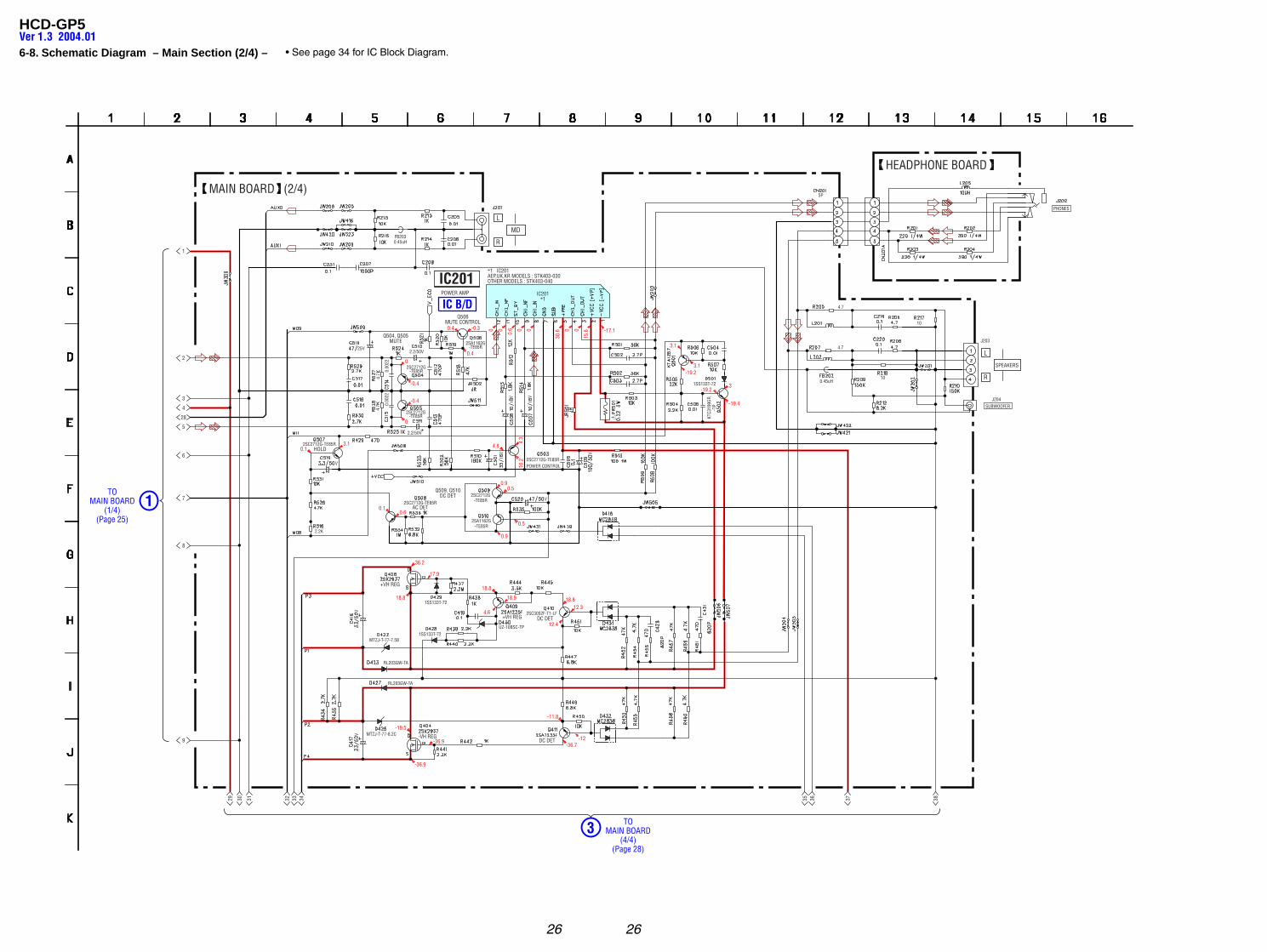
6-8. Schematic Diagram – Main Section (2/4) –
0.600-0.30.4
0.4
0
-0.4
-0.4
3.10.1
0
0 0 0 0
30.6
15.6 -17.1
0.10.6
0.50.9
4.8
4.3
10.2
0.9
0.5
36.2
17.9
18.9 18.812.3
18.8
4.6
12.4
18.8
-11.8
-19.5
-36.9
-36.7-12-36.9
-19.4
-19.23.1
-19.2
3.1
3
FB2030.45uH
25V
MD
R
L
IC201*1
*1 IC201AEP,UK,KR MODELS : STK403-030OTHER MODELS : STK403-040
PHONES
5P
4.7
4.7
0.45uH10
10
SPEAKERS
J203
SUBWOOFERJ204
V MTZJ-T-77-8.2C F
RL203GW-TA
RL203GW-TA
MTZJ-T-77-7.5B
V
1SS133T-72
1SS133T-72
UZ-10BSC-TP
F 2SC3052F-T1-LF
2SC2712G-TE85R
2SA1162G-TE85R
V2SC2712G-TE85R
2.2K
V
2SC2712G-TE85R
V V
KTC3
199G
R-T
P
1SS133T-72
V V
2.2/50V
2.2/50V
4.7
4.7
0.00
220.
0022
2SC2712G-TE85R
2SC2712G-TE85R
2SA1162G-TE85R
R
L
0
1
2
3
4
5
28
6
7
8
9
29 30 34333231 38373635
MAIN BOARD (2/4)
HEADPHONE BOARD
IC201POWER AMP
HOLD
AC DET
Q509, Q510DC DET
+VH REG
+VH REG
-VH REGDC DET
DC DET
Q506MUTE CONTROL
Q504, Q505MUTE
POWER CONTROL2SC2712G-TE85R
TOMAIN BOARD
(1/4)(Page 25)
1
TOMAIN BOARD
(4/4)(Page 28)
3
IC B/D
• See page 34 for IC Block Diagram.
Ver 1.3 2004.01

2727
HCD-GP5
6-9. Schematic Diagram – Main Section (3/4) –
3.4(-0.4)
3.8(0)
0(-0.4)
0
-0.2(-0.7)
3.7
(-0.
4)3.4(-0.4)
0
0
0(-0.4)0
0
10.3
10.2
10.2
10.3
9.89.8
0.7(4.9)
1.2(5.5)
1.2(6.9)
0.5
0.5
0.51.1
Q3082SK2158-T2B
D3011SS133T-72
Q3102SA1162-G
Q3072SK2158-T2B
Q3092SA1162-G
Q306DTA124EUA-T106
Q311DTA124EUA-T106
Q3052SK2158-T2B
C333100 / 16V
CN3017P
L301BIAS
OSCILLATION
Q3022SC5343GL
Q3012SC5343GL Q3
032S
C534
3GL
Q304
2SC3
052F
-T1-
LF
V
V V
Q4192SC3266GR
D421MTZJ-T-72-5.6B
R3310
C34610P
D302
UZ-
4.7B
SA-T
P
V
25V
25V
10 11 27262524232221201918171615141312
40
41
47
46
45
44
43
42
MAIN BOARD (3/4)
TAPE MECHANISMDECK
Q305 - Q311REC/PLAYSWITCH
Q301, Q302BIAS OSC
Q303, Q304BIAS SWITCH
REGULATOR
TOMAIN BOARD
(1/4)(Page 25)2
TOMAIN BOARD
(4/4)(Page 28)
4
7
• See page 18 for Waveform.
Ver 1.3 2004.01
2828
HCD-GP5
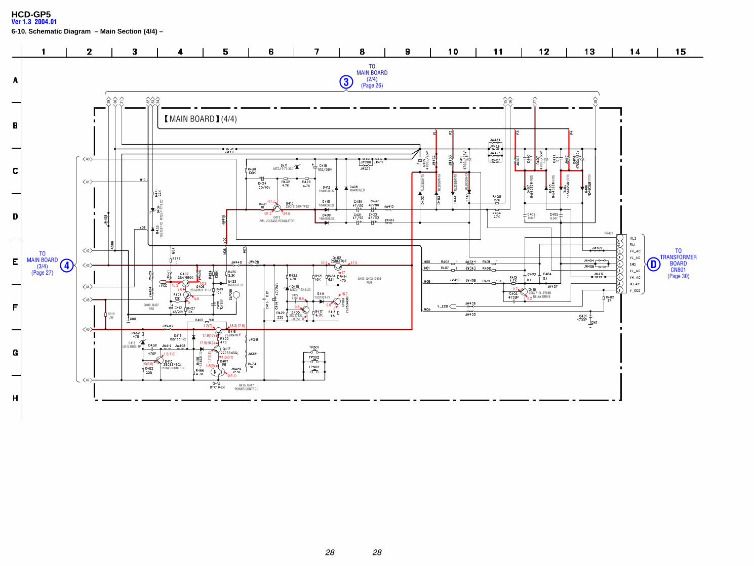
6-10. Schematic Diagram – Main Section (4/4) –
10.2 10.3
5.65
1.2(7)
17.9(17)
17.9(16.3)
1.6(0)
0(4.7)
1.5(0.1)
1.7(
0.8)
18.3(17.6)
1.8(1.0)
0(0.6)
9.6
17.5
17
10.3
16.20.9
0.6 0
0
0.6
-31.2
-31.7
-34.5
0.7
0.2
D418UZ-5.1BSB-TP
PN401
2SC2712L-TE85R
0.047 0.047
(F20
)
(F20
)
(F20
)
(F20
)
RL20
3GW
-TA
RL20
3GW
-TA
RL20
3GW
-TA
RL20
3GW
-TA
1N4003LES1N4003LES
1N4003LES
1N4003LES
V
2SC1815GR-TPE2
V
MTZJ-T-77-33D
-E
L1SS133T-72C427470P
2SC2712L-TE85L
MTZJ-T-72-8.2C
V1SS133T-72
50V
2SC3052F-T1-LF
G
0
VR319JW
L
T-72
T-72-E
L
1SS1
33T-
72M
TZJ-
T-77
-8.2
C
29
40
41
30 34333231 38373635
47
46
45
44
43
42
RELAY DRIVE
Q402, Q403, Q405REG
Q415, Q417POWER CONTROL
POWER CONTROL
Q406, Q407REG
Q413-VFL VOLTAGE REGULATOR
MAIN BOARD (4/4)
TOMAIN BOARD
(3/4)(Page 27)
4
TOMAIN BOARD
(2/4)(Page 26)3
TOTRANSFORMER
BOARDCN801
(Page 30)
D
Ver 1.3 2004.01

2929
HCD-GP5
6-11. Printed Wiring Board – Power Section – • See page 17 for Circuit Boards Location.
TRANSFORMER BOARD
TRANSFORMER BOARD
POWER TRANSFORMER
POWER TRANSFORMER
PT802POWER TRANSFORMER
(SUB)
PT802POWER TRANSFORMER
(SUB)
TOMAIN BOARD
PN401(Page 24)
1
2
JW80
7JW
806
TW
ACIN
TW
E51
E51
E51,TW
SW801
VOLTAGESELECTOR
230V
230V
ACIN
D
TOMAIN BOARD
PN401(Page 24)
D
1 2
EXCEPT E51,TW
Ver 1.3 2004.01

3030
HCD-GP5
PT801POWER TRANSFORMER
0
0RY801
POWER RELAYCN801
9P
PT802POWER TRANSFORMER (SUB)
0
0D802 1SS133T-72
D803 1SS133T-72
D801 1SS133T-72
D804 1SS133T-72
ACIN0
ACIN0
0
CN8022P
*
* not replaceablebult in transformer
L801LINE FILTER
E51E51
TW
TW
SW801
VOLTAGESELECTOR
TRANSFORMER BOARD
E51, TW
EXCEPT E51, TW
230V
120V
0L801
LINE FILTER
0
0
RY801POWER RELAY
PT802POWER TRANSFORMER (SUB)
0
PT801POWER TRANSFORMER
0
D802 1SS133T-72
D803 1SS133T-72
D801 1SS133T-72
D804 1SS133T-72
* * not replaceablebult in transformer
TRANSFORMER BOARD
CN8022P
CN8019P
TOMAIN
BOARD(4/4)
PN401(Page 28)
D
TOMAIN
BOARD(4/4)
PN401(Page 28)
D
6-12. Schematic Diagram – Power Section –Ver 1.3 2004.01

31
HCD-GP5
LEVEL SHIFT
INTERFACE
INTERFACE
INTERFACE
1 2 3 4 5 6 7 8 9 10 11 12 13 14
202122232425262728 19 18 17 16 15
F
RRF F
RRF
RR
F
FMUTE
THERMALSHUTDOWN
VREF
OUT
VREF
IN
POW
VCC
CH1F
IN
CH1R
IN
CH2F
IN
CH2R
IN
CH2O
UTR
CH2O
UTF
CH1O
UTR
CH1O
UTF
CAPA
IN1
CAPA
IN2
GND
PRFV
CC
MUT
E
POW
VCC
CH4S
IN'
CH4S
IN
CH4B
IN
CH3F
IN
CH3R
IN
CH3O
UTR
CH3O
UTF
CH4O
UTR
CH4O
UTF
CAPA
IN3
GND
• IC Block Diagrams
IC101 CXD3017Q
IC102 BA5974FP-E2
TERFDC
CEIGEN
AVSS
0
ADIO
AVDD
0
CLTV
FILO
AVSS
3
VSS
AVDD
3
DOUT
VDD
PCO
FILI
ASYO
ASYI
RFAC
BIAS
SSTP
DFCTMIRR
MDPLOCK
FOK
SFDR
VSS
TEST
FRDR
FEVC
COUT
SE
XTSLTES1
SRDRTFDR
FFDRTRDR
21
7071
6869
6667
64
65
62
61
63
7374
72
75
76
7778
7980
4
XRST
3
SQCK
SQSO
5 9876
5660 53545559 5758 5152 484950 47 444546 43 4142
XLAT
CLOK
SENS
SYSM
DATA
XUGF
XPCK GF
S
C2PO
WFC
K
10 11 12 13 14 15 16 17 18 19 20
21
222324
2526
3233
3031
3637
3435
3940
38
28
27
29
SPOA
ATSK
SCLK
VDD
SCOR
SPOB
XLON
XTAI
XVDD
EMPH
AVDD1AOUT1
AIN1
XTAOXVSS
AIN2
AOUT2AVDD2
RMUT
LOUT2
LOUT1
BCK
LRCK
PCMD
LMUT
AVSS1AVSS2
CPUINTERFACE
SERVO AUTOSEQUENCER
SERIAL ININTERFACE
OVER SAMPLINGDIGITAL FILTER
3rd ORDERNOISE SHAPER
PWM PWM
EFMDEMODULATOR
TIMINGLOGIC
DIGITALOUT
D/AINTERFACE
DIGITALPLL
ASYMMETRYCORRECTOR
CLOCKGENERATOR
MIRR, DFCT,FOK
DETECTOR
DIGITALCLV
SUBCODEPROCESSOR
SERVOINTERFACE
SERVO DSP
FOCUSSERVO
TRACKINGSERVO
SLEDSERVO
PWM GENERATOR
FOCUS PWMGENERATOR
TRACKINGPWM GENERATOR
SLED PWMGENERATOR
16KRAM
ERRORCORRECTOR
INTE
RNAL
BUS
A/DCONVERTER
OPERATIONALAMPLIFIER
ANALOG SWITCH
– CD Board –

32
HCD-GP5
IC103 CXA2581N-T4
RW/ROM
RW/ROM
EQ ON/OFF
VOFST
VOFSTDVC
VC
VC
VC
RW/ROM
VC
DVC
3029
28+–+
–
DVCVCC
DVC
27
262524
RW/ROM
EQ
23
22
21
20
19
RFACVCA
VCC
+–
DVC
+–
+–
RW/ROM
VC
RW/ROM
DVC
+–
3
A
B
C
D
BC
A
A
A
BCD
B C D D
+–
1
2 APC AMP
5
6789
4RFAC
SUMMINGAMP
RW/ROM
APC-OFF(Hi-Z)
RW/ROM(H/L)
VOFST
VC
RW/ROM
+–
10
11
GM
GM
18
17
16
B
D
A
C
13
14
15
12
EQ IN
LD
PD
GND
ABCD
AC SUM
E
F
DVCC
DVC
RFAC
SW
DC OFSTRFDCI
RFDCO
VC
RFCVFCBST
RFG
VCC
CEI
CE
TE BAL
TE
FEI
FE

33
HCD-GP5
RE
C-O
_L
RE
C-O
_R
TU
NE
R-R
TU
NE
R-L
CD
-L
AU
X-L
OU
T-L
OU
T-R
TO
N_L
-L
TO
N_L
-R
AU
X-R
CD
-R
VS
S
TO
N_H
-R
TO
N_H
-L
TAP
E-L
TAP
E-R
IC301 BD3881FV
– MAIN Board –
1 2 3 4 5 6 7 8 9
CONTROL LOGIC
TSD
VREF
OUT2
OUT1
RNF
VM VCC
FIN
GND
RIN
IC604 BA6956AN
– CONTROL Board –

34
HCD-GP5
IC201 STK403-040
PRE DRIVERIC CH1
1 2 3 4 5 6 7 8 9 10 11 12
PRE DRIVERIC CH2
BIAS CIRCUIT
–VCC
(–VP
)
+VCC
(+VP
)
CH1
OUT
CH2
OUT
+PRE SU
B
GND
CH1
IN
CH1
NF
ST B
Y
CH2
NF
CH2
IN
C4
C2C1
C3
TR4
TR6TR3
TR2 TR5
TR1
R5
R6
R1
R2
R3
R4
R7
R8
SUB

35
HCD-GP5
6-13. IC Pin Function DescriptionIC601 LC876764A-51E5 System Control (CONTROL Board)
Pin No.
1
2
3
4
5
6
7
8
9
10
11
12
13
14
15
16
17
18
19
20
21
22
23
24
25
26
27
28
29
30 to 33
34 to 44
45
46
47 to 50
51
52 to 66
67, 68
69 to 71
72
73
74
75
76
77
78
79
80
81
82
83
I/O
O
O
I
O
I
O
O
O
O
O
I
I
O
—
I
O
—
I
I
I
I
I
I
I
I
I
I
I
I
—
O
O
—
O
—
O
—
I
—
O
O
O
O
O
—
I
O
O
O
O
Pin Name
C-PWM1
C-PWM2
C-SCOR
T-SOL
T-END
T-MTR.CONT
O-SHIFT
P-CON
PAMP-MUTE
F-DATA
I-RESET
I-XT1
O-XT2
GND.
XIN
XOUT
VDD1
I-KEY1
I-KEY2
BASS ENC INPUT
TRBLE ENC INPUT
VOL-ENC
RDS-SIG
T-SW
I-POWER MONI
I-POWER DOWN
RDS-CLK
CD-DOOR-SW
RMC-IN
NC
O-GRID1 to 11
O-SEG1
VDD3
O-SEG2 to 5
GND.
O-SEG6 to 20
NC
I-INI-1 to 3
VDD4
O-CLOSE
O-OPEN
LED-CONT
O-DSG
T-REC
I-INI.BASS+2
T-PLAY.SW
R-MUTE
O-BIAS
CD-FUN
O-PWM3E
Description
PWM1 signal output to the CD unit
PWM2 signal output to the CD unit
SCOR (SUBQ request) signal output to the CD unit
Solenoid control signal output to the tape deck
Tape deck reel switch signal input
Motor control signal output to the tape deck
Clock shift control signal output
Power relay control signal output
Muting control signal output to the power amplifier
Control signal output to the sound processor
Reset signal input from the reset IC (IC603)
Resonator terminal (32.768kHz)
Resonator terminal (32.768kHz)
Ground terminal
Resonator terminal (8.64MHz)
Resonator terminal (8.64MHz)
Power supply terminal
Key AD input 1
Key AD input 2
Encoder signal input from the bass encoder
Encoder signal input from the treble encoder
Encoder signal input from the volume encoder
RDS signal level input from the tuner
Tape switch status signal input from the tape deck (SW2 to 4)
Power amplifier overload monitoring signal input
Power down detection signal input
RDS clock input from the tuner
CD door open/close switch signal input
Remote sensor signal input
Not used (open)
Grid signal output to the fluorescent indicator tube
Segment signal output to the fluorescent indicator tube
Power supply terminal
Segment signal output to the fluorescent indicator tube
Ground terminal
Segment signal output to the fluorescent indicator tube
Not used (open)
Initial selection signal input
Power supply terminal
CD tray close control signal output
CD tray open control signal output
Standby LED control signal output
Not used (open)
REC/PLAY control signal output to the REC/PLAY switch circuit
Not used (fixed at “L”)
Play switch signal input from the tape deck
Muting signal output to the tuner
Bias control signal output to the bias oscillation circuit
CD power supply control signal output
Tuner power supply control siganl output

36
HCD-GP5
Pin No.
84
85
86
87
88
89
90
91
92
93
94
95
96
97
98
99
100
I/O
O
O
O
O
O
—
—
I
I
I
I
O
I
O
O
I
O
Pin Name
R-CE
C-XRST
C-XLT
C-DATA
C-SQCK
VSS2
VDD2
RDS-DATA
R-ST
R-TUNED
C-SENS
C-LDON
C-SQSO
C-CLK
R-DATA
R-COUNT
R-CLK
Description
Tuner chip enable signal output to the tuner
Reset signal output to the CD unit
Latch signal output to the CD unit
Data output to the CD unit
SUBQ clock output to the CD unit
Ground terminal
Power supply terminal
RDS data input from the tuner
Stereo/mono detection signal input from the tuner
Tuner tuned status signal input
SENS signal input from the CD unit
LD ON signal output to the CD unit
SUB-Q data input from the CD unit
Clock output to the CD unit
Data output to the tuner
IF count signal input from the tuner
Clock signal output to the tuner

SECTION 7EXPLODED VIEWS
37
HCD-GP5
The components identified by mark 0 ordotted line with mark 0 are critical for safety.Replace only with part number specified.
Les composants identifiés par une marque0 sont critiques pour la sécurité.Ne les remplacer que par une pièce portantle numéro spécifié.
NOTE:• -XX, -X mean standardized parts, so they may
have some differences from the original one.• Items marked “*” are not stocked since they
are seldom required for routine service. Somedelay should be anticipated when ordering theseitems.
• The mechanical parts with no reference numberin the exploded views are not supplied.
• AbbreviationAUS : Australian modelCND : Canadian modelE51 : Chilean and Peruvian modelsHK : Hong Kong modelKR : Korean modelSP : Singapore modelTW : Taiwan model
Ref. No. Part No. Description Remark Ref. No. Part No. Description Remark
7-1. Overall Section
5
1
3
4
#3
#2
#2
#2
#2
#3
#3
a
a
#3
#1
#1
#1
front panel section
chassis section
CD mechanismdeck section
not supplied
not supplied
not supplied
b
b
2
6
1 4-247-756-01 CABINET, TOP (US,CND,AEP,UK,KR)1 4-247-756-21 CABINET, TOP (AUS,E51,HK,SP,TW)2 1-827-731-11 WIRE (FLAT TYPE)(11 CORE)(EXCEPT AEP,UK)2 1-828-984-11 WIRE (FLAT TYPE)(15 CORE)(AEP,UK)3 1-693-619-11 TUNER (FM/AM)(AEP,UK,KR)
3 1-693-620-11 TUNER (FM/AM)(AUS,E51,HK,SP,TW)3 1-693-624-11 TUNER (FM/AM)(US,CND)4 4-247-367-01 LID,CD
05 1-555-795-00 CORD, POWER (EXCEPT US,CND,TW,KR)05 1-769-079-22 CORD, POWER (KR)05 1-783-532-11 CORD, POWER (US,CND,TW)
6 1-827-714-11 WIRE (FLAT TYPE)(21 CORE)#1 7-685-248-14 SCREW +KTP 3X12 TYPE2 NON-SLIT
#2 7-685-647-79 SCREW +BVTP 3X10 TYPE2 NON-S#3 7-685-647-14 SCREW +BVTP 3X10 TYPE2 NON-S
Ver 1.5

38
HCD-GP5
Ref. No. Part No. Description Remark Ref. No. Part No. Description Remark
7-2. Front Panel Section
51
52
53
54
55
56 57
5859
6061
6263
64
65
66
6768
69
70
71
73
76
77
79
#2
#2
#2#2
#2
#2 #2
not supplied
not supplied
not supplied
not supplied
not supplied
not supplied
72
51 4-247-757-01 SPR-T,CASS52 X-4955-860-1 LID TC ASSY53 X-4955-859-1 HOLDER CASSETTE ASSY54 4-238-631-01 TAPE SPRING55 4-247-361-01 COVER, DISPLAY
56 4-247-374-01 WINDOW,DISPLAY57 4-247-366-01 CABINET, FRONT (AEP,UK)57 4-247-366-21 CABINET, FRONT (EXCEPT AEP,UK)58 4-247-376-01 POWER,INDICATER59 4-247-370-01 BUTTON,POWER
60 4-247-357-01 CAP, AUX61 4-247-358-01 CAP, CD62 4-247-359-01 CAP, TUNING63 4-247-356-01 CAP, VOL64 4-247-360-01 COVER, RING65 1-689-576-11 HEADPHONE BOARD
66 4-247-369-01 BUTTON,OPEN/CLOSE67 4-247-368-01 BUTTON,FUNCTION68 4-231-841-01 SPRING (HEART CAM-B)69 4-231-825-01 CAM (B), HEART70 4-242-318-01 OIL-DMPR, 70
71 4-247-752-01 RUBBER, FOOT72 1-829-747-11 WIRE (FLAT TYPE)(26 CORE)73 1-796-351-51 MECHANISM, SINGLE CASSETTE76 4-247-371-01 BUTTON,CD77 A-4747-954-A CONTROL BOARD, COMPLETE (AEP,UK,KR)
77 A-4747-960-A CONTROL BOARD, COMPLETE (US,CND)77 A-4748-774-A CONTROL BOARD, COMPLETE
(E51,HK,SP,TW,AUS)79 3-229-336-01 SCREW +BVWH TAPPING#2 7-685-647-79 SCREW +BVTP 3X10 TYPE2 NON-S
Ver 1.5

39
HCD-GP5
7-3. Chassis Section
not supplied
not supplied
PT801
not supplied
notsupplied
#2
#2
#4
#2
#2
#2
#2
#2
101
102
103
not supplied
101 4-247-752-01 RUBBER, FOOT102 1-689-574-11 TRANSFORMER BOARD103 A-4747-957-A MAIN BOARD, COMPLETE (AEP,UK,KR)103 A-4747-962-A MAIN BOARD, COMPLETE (US,CND)103 A-4748-777-A MAIN BOARD, COMPLETE (E51,HK,SP,TW,AUS)
0PT801 1-443-032-11 TRANSFORMER, POWER (US,CND)
0PT801 1-443-033-11 TRANSFORMER, POWER (AEP,UK)0PT801 1-443-034-11 TRANSFORMER, POWER (HK,SP,AUS)0PT801 1-443-036-11 TRANSFORMER, POWER (KR)0PT801 ––––––––––– TRANSFORMER, POWER (E51,TW)
#2 7-685-647-79 SCREW +BVTP 3X10 TYPE2 NON-S
#4 7-682-561-09 SCREW +B 4X8P
Ref. No. Part No. Description Remarks Ref. No. Part No. Description Remarks
The components identified bymark 0 or dotted line with mark0 are critical for safety.Replace only with part numberspecified.
Les composants identifiés parune marque 0 sont critiquespour la sécurité.Ne les remplacer que par unepièce portant le numéro spécifié.
Ver 1.4 2004.08

40
HCD-GP5
7-4. CD Mechanism Deck Setion
M901
#6
#7
151
152
153
154
155
156157
158
160
159
161
162
166
167
164
165
168
169
171
170
170
172
163
170
167
173
171
169
169
169
not supplied
not supplied
not supplied
optical pick-up(KSM-213D)
151 1-674-336-12 LOADING BOARD152 4-925-315-31 DAMPER153 4-224-894-22 TRAY (CDM55D)154 4-220-233-01 CAM (CDM55)155 4-221-815-11 ROLLER
156 4-220-237-01 GEAR (A)157 4-220-234-01 PULLEY (LDG)158 4-221-816-01 BELT (CDM55)159 4-227-598-01 SPACER (55)160 4-220-238-01 GEAR (B)
161 4-220-229-02 LEVER (SW)162 4-220-239-01 SPRING, TORSION163 A-4728-536-A CD BOARD, COMPLETE
164 A-473-508-2A MAGNET165 4-231-777-02 SHEET (KH2)166 4-244-962-01 HOLDER (C213)167 4-985-672-01 SCREW (+PTPWH M2.6), FLOATING168 4-229-358-01 SHAFT (BU21)
169 4-227-549-11 INSULATOR170 4-244-959-01 SPRING (T213), COMPRESSION171 4-231-151-01 STOPPER (BU)172 4-218-253-31 SCREW (M2.6), +BTTP173 1-757-055-11 WIRE, PARALLEL (FFC) (16 CORE)
M901 A-4735-337-A MOTOR (LD) ASSY (TRAY)#6 7-685-533-19 SCREW +BTP 2.6X6 TYPE2 N-S#7 7-621-255-32 SCREW +P 2X5
Ref. No. Part No. Description Remarks Ref. No. Part No. Description Remarks
Ver 1.2 2003.11

41
HCD-GP5
The components identified bymark 0 or dotted line with mark0 are critical for safety.Replace only with part numberspecified.
Les composants identifiés parune marque 0 sont critiquespour la sécurité.Ne les remplacer que par unepièce portant le numéro spécifié.
7-5. KSM-213D
601
Ref. No. Part No. Description Remarks
0601 A-4735-357-A BASE ASSY, OP (KSM-213D)
Ver 1.2 2003.11

Ref. No. Part No. Description Remarks Ref. No. Part No. Description Remarks
42
SECTION 8ELECTRICAL PARTS LIST
HCD-GP5
NOTE:• Due to standardization, replacements in the parts
list may be different from the parts specified inthe diagrams or the components used on the set.
• -XX, -X mean standardized parts, so they mayhave some difference from the original one.
• Items marked “*” are not stocked since they areseldom required for routine service. Some delayshould be anticipated when ordering these items.
• RESISTORSAll resistors are in ohms.METAL: metal-film resistorMETAL OXIDE: Metal Oxide-film resistorF: nonflammable
• CAPACITORS:uF: µF
• COILSuH: µH
• SEMICONDUCTORSIn each case, u: µ, for example:uA...: µA... , uPA... , µPA... ,uPB... , µPB... , uPC... , µPC... ,uPD..., µPD...
• AbbreviationAUS : Australian modelCND: Canadian modelE51 : Chilean and Peruvian models
When indicating parts by reference number,please include the board name.
The components identified by mark 0 ordotted line with mark 0 are critical for safety.Replace only with part number specified.
Les composants identifiés par une marque0 sont critiques pour la sécurité.Ne les remplacer que par une pièce portantle numéro spécifié.
HK : Hong Kong modelKR : Korean modelSP : Singapore modelTW : Taiwan model
A-4728-536-A CD BOARD, COMPLETE******************
< CAPACITOR >
C101 1-162-967-11 CERAMIC CHIP 0.0033uF 10% 50VC102 1-107-826-11 CERAMIC CHIP 0.1uF 10.00% 16VC103 1-162-962-11 CERAMIC CHIP 470PF 10% 50VC104 1-162-962-11 CERAMIC CHIP 470PF 10% 50VC108 1-107-826-11 CERAMIC CHIP 0.1uF 10.00% 16V
C109 1-162-965-11 CERAMIC CHIP 0.0015uF 10% 50VC110 1-162-967-11 CERAMIC CHIP 0.0033uF 10% 50VC111 1-162-927-11 CERAMIC CHIP 100PF 5% 50VC112 1-115-156-11 CERAMIC CHIP 1uF 10VC114 1-164-360-11 CERAMIC CHIP 0.1uF 16V
C116 1-126-382-11 ELECT 100uF 20.00% 16VC117 1-126-382-11 ELECT 100uF 20.00% 16VC118 1-162-964-11 CERAMIC CHIP 0.001uF 10% 50VC121 1-164-360-11 CERAMIC CHIP 0.1uF 16VC122 1-126-933-11 ELECT 100uF 20.00% 16V
C123 1-162-970-11 CERAMIC CHIP 0.01uF 10% 25VC124 1-125-891-11 CERAMIC CHIP 0.47uF 10.00% 10VC125 1-164-360-11 CERAMIC CHIP 0.1uF 16VC126 1-164-360-11 CERAMIC CHIP 0.1uF 16VC127 1-126-382-11 ELECT 100uF 20.00% 16V
C130 1-164-360-11 CERAMIC CHIP 0.1uF 16VC131 1-126-933-11 ELECT 100uF 20.00% 16VC133 1-162-921-11 CERAMIC CHIP 33PF 5% 50VC140 1-115-156-11 CERAMIC CHIP 1uF 10VC143 1-164-360-11 CERAMIC CHIP 0.1uF 16V
C145 1-164-360-11 CERAMIC CHIP 0.1uF 16VC146 1-107-826-11 CERAMIC CHIP 0.1uF 10.00% 16VC153 1-164-360-11 CERAMIC CHIP 0.1uF 16VC159 1-162-969-11 CERAMIC CHIP 0.0068uF 10% 25VC162 1-126-382-11 ELECT 100uF 20.00% 16V
C163 1-126-933-11 ELECT 100uF 20.00% 16VC165 1-164-360-11 CERAMIC CHIP 0.1uF 16VC167 1-162-920-11 CERAMIC CHIP 27PF 5% 50VC168 1-162-919-11 CERAMIC CHIP 22PF 5% 50VC171 1-115-412-11 CERAMIC CHIP 680PF 5.00% 25V
C172 1-162-927-11 CERAMIC CHIP 100PF 5% 50VC181 1-115-412-11 CERAMIC CHIP 680PF 5.00% 25VC182 1-162-927-11 CERAMIC CHIP 100PF 5% 50VC183 1-162-968-11 CERAMIC CHIP 0.0047uF 10% 50VC184 1-162-968-11 CERAMIC CHIP 0.0047uF 10% 50V
C185 1-125-891-11 CERAMIC CHIP 0.47uF 10.00% 10V
C190 1-115-156-11 CERAMIC CHIP 1uF 10VC191 1-126-933-11 ELECT 100uF 20.00% 16VC192 1-126-382-11 ELECT 100uF 20.00% 16VC193 1-126-382-11 ELECT 100uF 20.00% 16V
C194 1-164-360-11 CERAMIC CHIP 0.1uF 16VC196 1-164-360-11 CERAMIC CHIP 0.1uF 16VC197 1-107-826-11 CERAMIC CHIP 0.1uF 10.00% 16VC198 1-126-933-11 ELECT 100uF 20.00% 16V
< CONNECTOR >
CN101 1-770-528-31 CONNECTOR, FFC/FPC 21PCN102 1-779-466-11 CONNECTOR, FFC (LIF (NON-ZIF)) 16P
< DIODE >
D101 8-719-056-77 DIODE UDZ-TE-17-3.9B
< FERRITE BEAD >
FB101 1-469-144-21 FERRITE 0uHFB103 1-469-144-21 FERRITE 0uH
< IC >
IC101 8-752-402-31 IC CXD3017QIC102 8-759-549-28 IC BA5974FP-E2IC103 8-752-089-74 IC CXA2581N-T4
< JUMPER RESISTOR >
JR101 1-216-864-11 METAL CHIP 0
< TRANSISTOR >
Q101 8-729-049-31 TRANSISTOR 2SB710A-RTXQ102 8-729-920-85 TRANSISTOR 2SD1664-T100-QR
< RESISTOR >
R101 1-216-821-11 METAL CHIP 1K 5% 1/10WR102 1-216-845-11 METAL CHIP 100K 5% 1/10WR103 1-216-835-11 METAL CHIP 15K 5% 1/10WR104 1-216-839-11 METAL CHIP 33K 5% 1/10WR106 1-216-821-11 METAL CHIP 1K 5% 1/10W
R107 1-216-833-11 METAL CHIP 10K 5% 1/10WR108 1-216-827-11 METAL CHIP 3.3K 5% 1/10WR109 1-216-857-11 METAL CHIP 1M 5% 1/10WR111 1-216-846-11 METAL CHIP 120K 5% 1/10WR114 1-218-745-11 METAL CHIP 160K 5% 1/10W
R116 1-216-797-11 METAL CHIP 10 5% 1/10W
CDVer 1.3 2004.01

Ref. No. Part No. Description Remarks Ref. No. Part No. Description Remarks
43
HCD-GP5
R117 1-216-821-11 METAL CHIP 1K 5% 1/10WR118 1-216-809-11 METAL CHIP 100 5% 1/10WR119 1-216-826-11 METAL CHIP 2.7K 5% 1/10WR120 1-216-835-11 METAL CHIP 15K 5% 1/10W
R122 1-216-845-11 METAL CHIP 100K 5% 1/10WR123 1-216-833-11 METAL CHIP 10K 5% 1/10WR124 1-216-845-11 METAL CHIP 100K 5% 1/10WR131 1-216-813-11 METAL CHIP 220 5% 1/10WR143 1-216-836-11 METAL CHIP 18K 5% 1/10W
R144 1-216-836-11 METAL CHIP 18K 5% 1/10WR147 1-216-828-11 METAL CHIP 3.9K 5% 1/10WR148 1-216-797-11 METAL CHIP 10 5% 1/10WR149 1-216-797-11 METAL CHIP 10 5% 1/10WR150 1-216-833-11 METAL CHIP 10K 5% 1/10W
R151 1-216-845-11 METAL CHIP 100K 5% 1/10WR158 1-216-837-11 METAL CHIP 22K 5% 1/10WR159 1-216-837-11 METAL CHIP 22K 5% 1/10WR162 1-216-847-11 METAL CHIP 150K 5% 1/10WR171 1-216-837-11 METAL CHIP 22K 5% 1/10W
R172 1-216-837-11 METAL CHIP 22K 5% 1/10WR173 1-216-837-11 METAL CHIP 22K 5% 1/10WR181 1-216-837-11 METAL CHIP 22K 5% 1/10WR182 1-216-837-11 METAL CHIP 22K 5% 1/10WR183 1-216-837-11 METAL CHIP 22K 5% 1/10W
R190 1-216-813-11 METAL CHIP 220 5% 1/10WR191 1-216-839-11 METAL CHIP 33K 5% 1/10WR192 1-216-839-11 METAL CHIP 33K 5% 1/10WR193 1-216-846-11 METAL CHIP 120K 5% 1/10WR194 1-216-845-11 METAL CHIP 100K 5% 1/10W
R195 1-216-853-11 METAL CHIP 470K 5% 1/10WR196 1-216-825-11 METAL CHIP 2.2K 5% 1/10WR197 1-216-821-11 METAL CHIP 1K 5% 1/10W
< NETWORK >
RN101 1-233-576-11 RES, CHIP NETWORK 100
< SWITCH >
S101 1-771-853-11 SWITCH, DETECTION (LIMIT)
< VIBRATOR >
X101 1-767-226-11 VIBRATOR, CRYSTAL (16.9344)************************************************************
A-4747-954-A CONTROL BOARD, COMPLETE (AEP, UK, KR)************************
A-4747-960-A CONTROL BOARD, COMPLETE (US, CND)************************
A-4748-774-A CONTROL BOARD, COMPLETE (E51, HK, SP, TW, AUS)
************************
4-247-818-01 GUIDE (FL)4-247-819-01 HOLDER, SENSOR4-247-820-01 FILTER, FL
< CAPACITOR >
C604 1-162-927-11 CERAMIC CHIP 100PF 5% 50VC605 1-162-962-11 CERAMIC CHIP 470PF 10% 50VC606 1-126-963-11 ELECT 4.7uF 20.00% 50V
C607 1-126-963-11 ELECT 4.7uF 20.00% 50VC608 1-126-916-11 ELECT 1000uF 20.00% 6.3V
C609 1-127-876-21 CERAMIC 0.01uF 10% 50VC610 1-115-339-11 CERAMIC CHIP 0.1uF 10.00% 50VC611 1-124-584-00 ELECT 100uF 20% 10VC612 1-124-234-00 ELECT 22uF 20% 16VC613 1-164-156-11 CERAMIC CHIP 0.1uF 25V
C614 1-115-339-11 CERAMIC CHIP 0.1uF 10.00% 50VC615 1-115-339-11 CERAMIC CHIP 0.1uF 10.00% 50VC616 1-162-913-11 CERAMIC CHIP 8PF 0.50PF 50VC617 1-162-919-11 CERAMIC CHIP 22PF 5% 50VC618 1-162-921-11 CERAMIC CHIP 33PF 5% 50V
C619 1-162-913-11 CERAMIC CHIP 8PF 0.50PF 50VC620 1-162-970-11 CERAMIC CHIP 0.01uF 10% 25VC621 1-162-970-11 CERAMIC CHIP 0.01uF 10% 25VC622 1-162-970-11 CERAMIC CHIP 0.01uF 10% 25VC623 1-162-917-11 CERAMIC CHIP 15PF 5% 50V
C624 1-126-947-11 ELECT 47uF 20.00% 25VC625 1-162-964-11 CERAMIC CHIP 0.001uF 10% 50VC626 1-162-921-11 CERAMIC CHIP 33PF 5% 50VC627 1-126-964-11 ELECT 10uF 20.00% 50VC628 1-115-339-11 CERAMIC CHIP 0.1uF 10.00% 50V
C629 1-162-927-11 CERAMIC CHIP 100PF 5% 50VC630 1-162-927-11 CERAMIC CHIP 100PF 5% 50VC631 1-162-282-31 CERAMIC 100PF 10% 50VC632 1-162-282-31 CERAMIC 100PF 10% 50VC633 1-162-927-11 CERAMIC CHIP 100PF 5% 50V
C634 1-162-927-11 CERAMIC CHIP 100PF 5% 50VC635 1-162-927-11 CERAMIC CHIP 100PF 5% 50VC636 1-162-927-11 CERAMIC CHIP 100PF 5% 50VC637 1-162-927-11 CERAMIC CHIP 100PF 5% 50VC638 1-162-927-11 CERAMIC CHIP 100PF 5% 50V
C639 1-162-970-11 CERAMIC CHIP 0.01uF 10% 25VC640 1-162-970-11 CERAMIC CHIP 0.01uF 10% 25VC641 1-126-960-11 ELECT 1uF 20.00% 50VC642 1-126-963-11 ELECT 4.7uF 20.00% 50VC643 1-115-339-11 CERAMIC CHIP 0.1uF 10.00% 50V
C644 1-115-339-11 CERAMIC CHIP 0.1uF 10.00% 50VC645 1-162-282-31 CERAMIC 100PF 10% 50VC646 1-126-964-11 ELECT 10uF 20.00% 50VC647 1-115-339-11 CERAMIC CHIP 0.1uF 10.00% 50VC648 1-115-339-11 CERAMIC CHIP 0.1uF 10.00% 50V
C649 1-162-970-11 CERAMIC CHIP 0.01uF 10% 25VC650 1-126-933-11 ELECT 100uF 20.00% 16VC651 1-162-282-31 CERAMIC 100PF 10% 50VC652 1-162-970-11 CERAMIC CHIP 0.01uF 10% 25VC653 1-162-970-11 CERAMIC CHIP 0.01uF 10% 25V
< CONNECTOR >
CN601 1-779-294-11 CONNECTOR, FFC (LIF (NON-ZIF)) 26PCN602 1-779-550-21 CONNECTOR, FFC (LIF (NON-ZIF)) 13P
* CN603 1-770-516-31 CONNECTOR, FFC/FPC 8P
< DIODE >
D601 8-719-010-41 DIODE UZ-5.6BSA-TPD602 8-719-991-33 DIODE 1SS133T-72D603 8-719-991-33 DIODE 1SS133T-77D604 8-719-991-33 DIODE 1SS133T-72
CD CONTROLVer 1.3 2004.01

Ref. No. Part No. Description Remarks Ref. No. Part No. Description Remarks
44
HCD-GP5
D605 8-719-991-33 DIODE 1SS133T-72
D606 8-719-991-33 DIODE 1SS133T-72D607 8-719-991-33 DIODE 1SS133T-72D608 8-719-989-91 DIODE 1N4148A-T265D609 8-719-989-91 DIODE 1N4148A-T265
< FERRITE BEAD >
FB601 1-412-473-21 INDUCTOR 0uH
< FLUORESCENT INDICATOR TUBE >
FL601 1-518-908-11 INDICATOR TUBE, FLUORESCENT
< IC >
IC601 6-803-170-01 IC LC876764C-51E5IC602 6-700-250-01 IC PST3445ULIC603 6-701-681-01 IC RPM7140-V4 (g)IC604 8-759-598-69 IC BA6956AN
< JUMPER RESISTOR >
JR601 1-216-864-11 METAL CHIP 0 5% 1/16WJR602 1-216-864-11 METAL CHIP 0 5% 1/16WJR604 1-216-864-11 METAL CHIP 0 5% 1/16WJR607 1-216-864-11 METAL CHIP 0 5% 1/16W
< COIL >
L601 1-410-509-11 INDUCTOR 10uHL602 1-410-509-11 INDUCTOR 10uH
< DIODE >
LED601 8-719-059-98 DIODE SLR-342VCT31
< TRANSISTOR >
Q601 8-729-230-49 TRANSISTOR 2SC2712L-TE85RQ602 6-550-296-01 TRANSISTOR 2SA1980GQ603 8-729-230-49 TRANSISTOR 2SC2712L-TE85RQ604 8-729-230-49 TRANSISTOR 2SC2712L-TE85RQ605 6-550-297-01 TRANSISTOR 2SA1981Y
Q606 6-550-305-01 TRANSISTOR 2SA1296GR- (TPE2)Q607 8-729-900-53 TRANSISTOR DTC114EKQ608 6-550-297-01 TRANSISTOR 2SA1981Y
< RESISTOR >
R601 1-216-828-11 METAL CHIP 3.9K 5% 1/16W (E51, HK, SP, TW, AUS)
R601 1-216-833-11 METAL CHIP 10K 5% 1/16W (US, CND, AEP, UK, KR)
R602 1-216-821-11 METAL CHIP 1K 5% 1/16WR603 1-216-821-11 METAL CHIP 1K 5% 1/16WR604 1-216-821-11 METAL CHIP 1K 5% 1/16W
R605 1-216-821-11 METAL CHIP 1K 5% 1/16WR606 1-216-841-11 METAL CHIP 47K 5% 1/16WR607 1-247-807-31 CARBON 100 5% 1/4WR608 1-247-807-31 CARBON 100 5% 1/4WR609 1-216-809-11 METAL CHIP 100 5% 1/16W
R610 1-216-809-11 METAL CHIP 100 5% 1/16WR611 1-216-809-11 METAL CHIP 100 5% 1/16WR612 1-249-429-11 CARBON 10K 5% 1/4W
R613 1-247-831-91 CARBON 1K 5% 1/4WR614 1-247-831-91 CARBON 1K 5% 1/4W
R615 1-247-831-91 CARBON 1K 5% 1/4WR616 1-247-831-91 CARBON 1K 5% 1/4WR617 1-247-831-91 CARBON 1K 5% 1/4WR618 1-247-831-91 CARBON 1K 5% 1/4WR619 1-216-845-11 METAL CHIP 100K 5% 1/16W
R620 1-216-829-11 METAL CHIP 4.7K 5% 1/16WR621 1-216-821-11 METAL CHIP 1K 5% 1/16WR622 1-216-835-11 METAL CHIP 15K 5% 1/16WR623 1-216-817-11 METAL CHIP 470 5% 1/16WR624 1-216-833-11 METAL CHIP 10K 5% 1/16W
R625 1-216-825-11 METAL CHIP 2.2K 5% 1/16WR626 1-216-833-11 METAL CHIP 10K 5% 1/16WR627 1-216-825-11 METAL CHIP 2.2K 5% 1/16WR629 1-249-436-11 CARBON 39K 5% 1/4WR631 1-216-837-11 METAL CHIP 22K 5% 1/16W
(E51, HK, SP, TW, AUS)
R632 1-216-845-11 METAL CHIP 100K 5% 1/16WR633 1-216-845-11 METAL CHIP 100K 5% 1/16WR634 1-216-833-11 METAL CHIP 10K 5% 1/16WR635 1-216-845-11 METAL CHIP 100K 5% 1/16WR636 1-216-845-11 METAL CHIP 100K 5% 1/16W
R637 1-216-845-11 METAL CHIP 100K 5% 1/16WR638 1-216-845-11 METAL CHIP 100K 5% 1/16WR639 1-216-845-11 METAL CHIP 100K 5% 1/16WR640 1-216-845-11 METAL CHIP 100K 5% 1/16WR641 1-216-845-11 METAL CHIP 100K 5% 1/16W
R642 1-216-845-11 METAL CHIP 100K 5% 1/16WR643 1-216-845-11 METAL CHIP 100K 5% 1/16WR644 1-216-845-11 METAL CHIP 100K 5% 1/16WR645 1-216-845-11 METAL CHIP 100K 5% 1/16WR646 1-216-845-11 METAL CHIP 100K 5% 1/16W
R647 1-216-845-11 METAL CHIP 100K 5% 1/16WR648 1-216-845-11 METAL CHIP 100K 5% 1/16WR649 1-216-845-11 METAL CHIP 100K 5% 1/16WR650 1-216-845-11 METAL CHIP 100K 5% 1/16WR651 1-216-845-11 METAL CHIP 100K 5% 1/16W
R652 1-216-845-11 METAL CHIP 100K 5% 1/16WR653 1-216-845-11 METAL CHIP 100K 5% 1/16WR654 1-216-845-11 METAL CHIP 100K 5% 1/16WR655 1-216-845-11 METAL CHIP 100K 5% 1/16WR656 1-216-845-11 METAL CHIP 100K 5% 1/16W
R657 1-216-845-11 METAL CHIP 100K 5% 1/16WR658 1-216-845-11 METAL CHIP 100K 5% 1/16WR659 1-216-835-11 METAL CHIP 15K 5% 1/16WR660 1-216-845-11 METAL CHIP 100K 5% 1/16WR661 1-216-845-11 METAL CHIP 100K 5% 1/16W
R662 1-216-841-11 METAL CHIP 47K 5% 1/16WR663 1-216-841-11 METAL CHIP 47K 5% 1/16WR664 1-247-887-00 CARBON 220K 5% 1/4WR665 1-216-841-11 METAL CHIP 47K 5% 1/16WR666 1-216-821-11 METAL CHIP 1K 5% 1/16W
R667 1-216-853-11 METAL CHIP 470K 5% 1/16WR668 1-216-809-11 METAL CHIP 100 5% 1/16WR669 1-216-829-11 METAL CHIP 4.7K 5% 1/16WR670 1-216-833-11 METAL CHIP 10K 5% 1/16WR671 1-216-841-11 METAL CHIP 47K 5% 1/16W
CONTROLVer 1.3 2004.01

Ref. No. Part No. Description Remarks Ref. No. Part No. Description Remarks
45
HCD-GP5
R672 1-216-841-11 METAL CHIP 47K 5% 1/16WR673 1-216-298-00 METAL CHIP 2.2 5% 1/10WR674 1-216-833-11 METAL CHIP 10K 5% 1/16WR675 1-216-837-11 METAL CHIP 22K 5% 1/16WR676 1-216-837-11 METAL CHIP 22K 5% 1/16W
R677 1-216-839-11 METAL CHIP 33K 5% 1/16WR678 1-216-837-11 METAL CHIP 22K 5% 1/16WR679 1-218-179-11 RES-CHIP 10M 5% 1/10WR680 1-247-831-91 CARBON 1K 5% 1/4WR681 1-216-821-11 METAL CHIP 1K 5% 1/16W
R682 1-249-410-11 CARBON 270 5% 1/4W FR683 1-216-845-11 METAL CHIP 100K 5% 1/16WR684 1-249-426-11 CARBON 5.6K 5% 1/4WR685 1-216-845-11 METAL CHIP 100K 5% 1/16WR686 1-218-817-11 RES-CHIP 3.3 10% 1/2W
R687 1-249-426-11 CARBON 5.6K 5% 1/4WR688 1-249-429-11 CARBON 10K 5% 1/4WR689 1-216-809-11 METAL CHIP 100 5% 1/16WR690 1-216-809-11 METAL CHIP 100 5% 1/16WR691 1-247-807-31 CARBON 100 5% 1/4W
R692 1-216-809-11 METAL CHIP 100 5% 1/16WR693 1-216-809-11 METAL CHIP 100 5% 1/16WR694 1-216-809-11 METAL CHIP 100 5% 1/16WR695 1-216-809-11 METAL CHIP 100 5% 1/16WR696 1-216-809-11 METAL CHIP 100 5% 1/16W
R697 1-247-807-31 CARBON 100 5% 1/4WR698 1-247-807-31 CARBON 100 5% 1/4WR699 1-247-807-31 CARBON 100 5% 1/4WR700 1-216-837-11 METAL CHIP 22K 5% 1/16W
(E51, HK, SP, TW, AUS)R700 1-216-295-91 SHORT CHIP 0 (US, CND, AEP, UK, KR)
R701 1-216-833-11 METAL CHIP 10K 5% 1/16W (US, CND, AEP, UK, KR)
R702 1-216-837-11 METAL CHIP 22K 5% 1/16W (E51, HK, SP, TW, AUS)
R702 1-247-831-91 CARBON 1K 5% 1/4W (US, CND, AEP, UK, KR)
R703 1-249-425-11 CARBON 4.7K 5% 1/4W FR704 1-249-425-11 CARBON 4.7K 5% 1/4W F
R705 1-216-845-11 METAL CHIP 100K 5% 1/16WR706 1-218-867-11 METAL CHIP 6.8K 5% 1/10WR707 1-249-430-11 CARBON 12K 5% 1/4WR708 1-216-840-11 METAL CHIP 39K 5% 1/16WR709 1-216-833-11 METAL CHIP 10K 5% 1/16W
R710 1-247-831-91 CARBON 1K 5% 1/4WR711 1-218-833-11 METAL CHIP 270 0.5% 1/10WR712 1-247-831-91 CARBON 1K 5% 1/4WR713 1-249-419-11 CARBON 1.5K 5% 1/4W FR714 1-216-824-11 METAL CHIP 1.8K 5% 1/16W
R715 1-249-422-11 CARBON 2.7K 5% 1/4W FR716 1-216-828-11 METAL CHIP 3.9K 5% 1/16WR717 1-249-427-11 CARBON 6.8K 5% 1/4W FR718 1-249-430-11 CARBON 12K 5% 1/4WR719 1-249-419-11 CARBON 1.5K 5% 1/4W F
R720 1-216-824-11 METAL CHIP 1.8K 5% 1/16WR721 1-249-422-11 CARBON 2.7K 5% 1/4W FR722 1-216-828-11 METAL CHIP 3.9K 5% 1/16WR723 1-247-831-91 CARBON 1K 5% 1/4WR724 1-249-426-11 CARBON 5.6K 5% 1/4W
R725 1-216-845-11 METAL CHIP 100K 5% 1/16WR726 1-216-829-11 METAL CHIP 4.7K 5% 1/16WR727 1-216-845-11 METAL CHIP 100K 5% 1/16WR728 1-216-845-11 METAL CHIP 100K 5% 1/16WR729 1-247-831-91 CARBON 1K 5% 1/4W
R734 1-216-838-11 METAL CHIP 27K 5% 1/16WR735 1-247-879-91 CARBON 100K 5% 1/4WR736 1-247-879-91 CARBON 100K 5% 1/4W
< SWITCH >
S601 1-786-050-21 SWITCH, KEY BOARD (TUNER/BAND)S602 1-786-050-21 SWITCH, KEY BOARD (bB TAPE)S603 1-786-050-21 SWITCH, KEY BOARD (MD)S604 1-786-050-21 SWITCH, KEY BOARD (Z)S605 1-786-050-21 SWITCH, KEY BOARD (x)
S606 1-786-050-21 SWITCH, KEY BOARD (+ M>)S607 1-786-050-21 SWITCH, KEY BOARD (.m –)S608 1-786-050-21 SWITCH, KEY BOARD (~/1)S609 1-786-050-21 SWITCH, KEY BOARD (DISPLAY)S610 1-786-050-21 SWITCH, KEY BOARD
(PLAY MODE/TUNING MODE)
S611 1-786-050-21 SWITCH, KEY BOARD (CD SYNC)S612 1-786-050-21 SWITCH, KEY BOARD (z REC PAUSE/START)S613 1-786-050-21 SWITCH, KEY BOARD (CD u)S614 1-786-050-21 SWITCH, KEY BOARD (DSG)S615 1-786-050-21 SWITCH, KEY BOARD (VOL+)
S616 1-786-050-21 SWITCH, KEY BOARD (VOL-)
< VIBRATOR >
X601 9-300-001-87 VIB, XTAL 32.768KHZ CFS-308 CT 32.768KHzX602 1-795-880-11 VIBRATOR, CERAMIC 8.64MHz
************************************************************
1-689-576-11 HEADPHONE BOARD*****************
< JACK >
J202 1-816-219-11 JACK, HEADPHONE (PHONES)
< COIL >
L205 1-408-117-00 INDUCTOR 10uH
< RESISTOR >
R201 1-249-409-11 CARBON 220 5% 1/4W FR202 1-249-412-11 CARBON 390 5% 1/4W FR203 1-249-409-11 CARBON 220 5% 1/4W FR204 1-249-412-11 CARBON 390 5% 1/4W F
************************************************************
1-674-336-12 LOADING BOARD**************
< CONNECTOR >
* CN151 1-568-943-11 PIN, CONNECTOR 5P
< SWITCH >
S1 1-786-203-11 SWITCH, LEVER (SLIDE)(OPEN/CLOSE)************************************************************
CONTROL HEADPHONE LOADINGVer 1.3 2004.01

Ref. No. Part No. Description Remarks Ref. No. Part No. Description Remarks
46
HCD-GP5
A-4747-957-A MAIN BOARD, COMPLETE (AEP, UK, KR)*********************
A-4747-962-A MAIN BOARD, COMPLETE (US, CND)*********************
A-4748-777-A MAIN BOARD, COMPLETE(E51, HK, SP, TW, AUS)
*********************
< CAPACITOR >
C205 1-162-970-11 CERAMIC CHIP 0.01uF 10% 25VC206 1-162-970-11 CERAMIC CHIP 0.01uF 10% 25VC207 1-162-964-11 CERAMIC CHIP 0.001uF 10% 50VC208 1-164-156-11 CERAMIC CHIP 0.1uF 25VC219 1-164-156-11 CERAMIC CHIP 0.1uF 25V
C220 1-164-156-11 CERAMIC CHIP 0.1uF 25VC231 1-164-156-11 CERAMIC CHIP 0.1uF 25VC301 1-162-964-11 CERAMIC CHIP 0.001uF 10% 50VC302 1-162-964-11 CERAMIC CHIP 0.001uF 10% 50VC305 1-106-361-00 MYLAR 0.0056uF 5.00% 100V
C306 1-126-923-91 ELECT 220uF 20.00% 10VC307 1-162-970-11 CERAMIC CHIP 0.01uF 10% 25VC308 1-162-979-11 CERAMIC CHIP 0.0027uF 10.00% 50VC309 1-162-979-11 CERAMIC CHIP 0.0027uF 10.00% 50VC310 1-162-979-11 CERAMIC CHIP 0.0027uF 10.00% 50V
C311 1-164-156-11 CERAMIC CHIP 0.1uF 25VC312 1-164-156-11 CERAMIC CHIP 0.1uF 25VC313 1-162-964-11 CERAMIC CHIP 0.001uF 10% 50V
(AEP, UK, KR)C314 1-164-156-11 CERAMIC CHIP 0.1uF 25VC315 1-124-589-11 ELECT 47uF 20% 16V
C316 1-162-915-11 CERAMIC CHIP 10PF 0.5PF 50VC317 1-126-923-91 ELECT 220uF 20.00% 10VC318 1-162-970-11 CERAMIC CHIP 0.01uF 10% 25VC319 1-126-947-11 ELECT 47uF 20.00% 16VC320 1-162-967-11 CERAMIC CHIP 0.0033uF 10% 50V
C321 1-162-967-11 CERAMIC CHIP 0.0033uF 10% 50VC322 1-126-961-11 ELECT 2.2uF 20.00% 50VC323 1-126-961-11 ELECT 2.2uF 20.00% 50VC324 1-164-315-11 CERAMIC CHIP 470PF 5.00% 50VC325 1-162-969-11 CERAMIC CHIP 0.0068uF 10% 25V
C326 1-162-969-11 CERAMIC CHIP 0.0068uF 10% 25VC327 1-164-315-11 CERAMIC CHIP 470PF 5.00% 50VC328 1-162-923-11 CERAMIC CHIP 47PF 5% 50VC329 1-162-923-11 CERAMIC CHIP 47PF 5% 50VC330 1-126-947-11 ELECT 47uF 20.00% 25V
C331 1-126-947-11 ELECT 47uF 20.00% 25VC332 1-164-733-11 CERAMIC CHIP 820PF 10.00% 50VC333 1-126-933-11 ELECT 100uF 20.00% 16VC334 1-164-733-11 CERAMIC CHIP 820PF 10.00% 50VC335 1-164-230-11 CERAMIC CHIP 220PF 5.00% 50V
C338 1-126-160-11 ELECT 1uF 20% 50VC339 1-126-160-11 ELECT 1uF 20% 50VC341 1-162-968-11 CERAMIC CHIP 0.0047uF 10% 50VC344 1-126-947-11 ELECT 47uF 20.00% 25VC345 1-104-658-91 ELECT 100uF 20.00% 10V
(AEP, UK, KR)
C346 1-162-199-31 CERAMIC 10PF 5% 50VC351 1-126-963-11 ELECT 4.7uF 20.00% 50VC352 1-126-956-91 ELECT 0.1uF 20.00% 50V
C353 1-126-956-91 ELECT 0.1uF 20.00% 50VC354 1-124-464-11 ELECT 0.22uF 20% 50V
C355 1-124-464-11 ELECT 0.22uF 20% 50VC356 1-124-464-11 ELECT 0.22uF 20% 50VC357 1-126-957-11 ELECT 0.22uF 20.00% 50VC358 1-126-963-11 ELECT 4.7uF 20.00% 50VC359 1-164-315-11 CERAMIC CHIP 470PF 5.00% 50V
C360 1-162-977-11 CERAMIC CHIP 0.0018uF 10.00% 50VC361 1-162-977-11 CERAMIC CHIP 0.0018uF 10.00% 50VC362 1-164-315-11 CERAMIC CHIP 470PF 5.00% 50VC363 1-164-218-11 CERAMIC CHIP 180PF 0.25PF 50VC364 1-164-218-11 CERAMIC CHIP 180PF 0.25PF 50V
C367 1-164-315-11 CERAMIC CHIP 470PF 5.00% 50VC368 1-164-315-11 CERAMIC CHIP 470PF 5.00% 50VC384 1-162-970-11 CERAMIC CHIP 0.01uF 10% 25VC385 1-162-964-11 CERAMIC CHIP 0.001uF 10% 50VC387 1-162-964-11 CERAMIC CHIP 0.001uF 10% 50V
C390 1-162-964-11 CERAMIC CHIP 0.001uF 10% 50VC392 1-164-156-11 CERAMIC CHIP 0.1uF 25VC396 1-128-801-21 CERAMIC 22PF 5% 50VC397 1-164-733-11 CERAMIC CHIP 820PF 10.00% 50VC398 1-164-733-11 CERAMIC CHIP 820PF 10.00% 50V
C401 1-162-968-11 CERAMIC CHIP 0.0047uF 10% 50VC402 1-162-968-11 CERAMIC CHIP 0.0047uF 10% 50VC403 1-115-339-11 CERAMIC CHIP 0.1uF 10.00% 50VC404 1-115-339-11 CERAMIC CHIP 0.1uF 10.00% 50VC405 1-137-420-11 FILM 0.047uF 5.00% 100V
C406 1-137-420-11 FILM 0.047uF 5.00% 100VC407 1-119-940-51 ELECT 4700uF 20.00% 50VC408 1-119-940-51 ELECT 4700uF 20.00% 50VC409 1-128-548-11 ELECT 4700uF 20.00% 25VC410 1-128-548-11 ELECT 4700uF 20.00% 25V
C412 1-126-947-11 ELECT 47uF 20.00% 25VC413 1-162-970-11 CERAMIC CHIP 0.01uF 10% 25VC414 1-126-947-11 ELECT 47uF 20.00% 25VC416 1-126-966-11 ELECT 33uF 20.00% 50VC417 1-126-966-11 ELECT 33uF 20.00% 50V
C418 1-126-968-11 ELECT 100uF 20.00% 50VC419 1-164-156-11 CERAMIC CHIP 0.1uF 25VC420 1-124-261-00 ELECT 10uF 20% 50VC421 1-126-967-11 ELECT 47uF 20.00% 50VC422 1-126-967-11 ELECT 47uF 20.00% 50V
C424 1-124-584-00 ELECT 100uF 20% 10VC427 1-164-315-11 CERAMIC CHIP 470PF 5.00% 50VC428 1-164-733-11 CERAMIC CHIP 820PF 10.00% 50VC431 1-164-733-11 CERAMIC CHIP 820PF 10.00% 50VC432 1-124-589-11 ELECT 47uF 20% 16V
C433 1-124-584-00 ELECT 100uF 20% 10VC434 1-162-970-11 CERAMIC CHIP 0.01uF 10% 25VC435 1-124-589-11 ELECT 47uF 20% 16VC436 1-126-967-11 ELECT 47uF 20.00% 50VC437 1-126-967-11 ELECT 47uF 20.00% 50V
C438 1-164-315-11 CERAMIC CHIP 470PF 5.00% 50VC439 1-162-970-11 CERAMIC CHIP 0.01uF 10% 25VC440 1-130-321-11 FILM 0.1uF 5.00% 100VC441 1-130-321-11 FILM 0.1uF 5.00% 100VC501 1-126-966-11 ELECT 33uF 20.00% 16V
MAINVer 1.3 2004.01
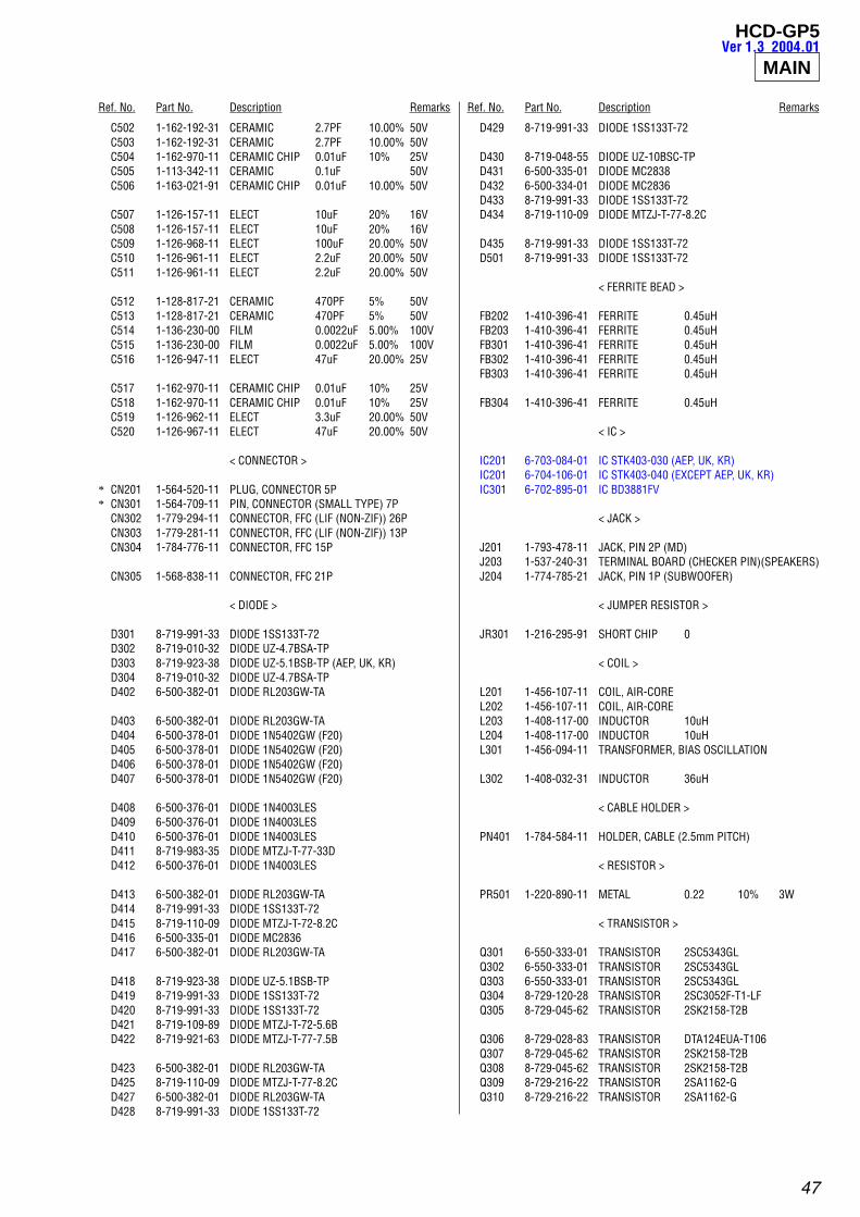
Ref. No. Part No. Description Remarks Ref. No. Part No. Description Remarks
47
HCD-GP5
C502 1-162-192-31 CERAMIC 2.7PF 10.00% 50VC503 1-162-192-31 CERAMIC 2.7PF 10.00% 50VC504 1-162-970-11 CERAMIC CHIP 0.01uF 10% 25VC505 1-113-342-11 CERAMIC 0.1uF 50VC506 1-163-021-91 CERAMIC CHIP 0.01uF 10.00% 50V
C507 1-126-157-11 ELECT 10uF 20% 16VC508 1-126-157-11 ELECT 10uF 20% 16VC509 1-126-968-11 ELECT 100uF 20.00% 50VC510 1-126-961-11 ELECT 2.2uF 20.00% 50VC511 1-126-961-11 ELECT 2.2uF 20.00% 50V
C512 1-128-817-21 CERAMIC 470PF 5% 50VC513 1-128-817-21 CERAMIC 470PF 5% 50VC514 1-136-230-00 FILM 0.0022uF 5.00% 100VC515 1-136-230-00 FILM 0.0022uF 5.00% 100VC516 1-126-947-11 ELECT 47uF 20.00% 25V
C517 1-162-970-11 CERAMIC CHIP 0.01uF 10% 25VC518 1-162-970-11 CERAMIC CHIP 0.01uF 10% 25VC519 1-126-962-11 ELECT 3.3uF 20.00% 50VC520 1-126-967-11 ELECT 47uF 20.00% 50V
< CONNECTOR >
* CN201 1-564-520-11 PLUG, CONNECTOR 5P* CN301 1-564-709-11 PIN, CONNECTOR (SMALL TYPE) 7P
CN302 1-779-294-11 CONNECTOR, FFC (LIF (NON-ZIF)) 26PCN303 1-779-281-11 CONNECTOR, FFC (LIF (NON-ZIF)) 13PCN304 1-784-776-11 CONNECTOR, FFC 15P
CN305 1-568-838-11 CONNECTOR, FFC 21P
< DIODE >
D301 8-719-991-33 DIODE 1SS133T-72D302 8-719-010-32 DIODE UZ-4.7BSA-TPD303 8-719-923-38 DIODE UZ-5.1BSB-TP (AEP, UK, KR)D304 8-719-010-32 DIODE UZ-4.7BSA-TPD402 6-500-382-01 DIODE RL203GW-TA
D403 6-500-382-01 DIODE RL203GW-TAD404 6-500-378-01 DIODE 1N5402GW (F20)D405 6-500-378-01 DIODE 1N5402GW (F20)D406 6-500-378-01 DIODE 1N5402GW (F20)D407 6-500-378-01 DIODE 1N5402GW (F20)
D408 6-500-376-01 DIODE 1N4003LESD409 6-500-376-01 DIODE 1N4003LESD410 6-500-376-01 DIODE 1N4003LESD411 8-719-983-35 DIODE MTZJ-T-77-33DD412 6-500-376-01 DIODE 1N4003LES
D413 6-500-382-01 DIODE RL203GW-TAD414 8-719-991-33 DIODE 1SS133T-72D415 8-719-110-09 DIODE MTZJ-T-72-8.2CD416 6-500-335-01 DIODE MC2836D417 6-500-382-01 DIODE RL203GW-TA
D418 8-719-923-38 DIODE UZ-5.1BSB-TPD419 8-719-991-33 DIODE 1SS133T-72D420 8-719-991-33 DIODE 1SS133T-72D421 8-719-109-89 DIODE MTZJ-T-72-5.6BD422 8-719-921-63 DIODE MTZJ-T-77-7.5B
D423 6-500-382-01 DIODE RL203GW-TAD425 8-719-110-09 DIODE MTZJ-T-77-8.2CD427 6-500-382-01 DIODE RL203GW-TAD428 8-719-991-33 DIODE 1SS133T-72
D429 8-719-991-33 DIODE 1SS133T-72
D430 8-719-048-55 DIODE UZ-10BSC-TPD431 6-500-335-01 DIODE MC2838D432 6-500-334-01 DIODE MC2836D433 8-719-991-33 DIODE 1SS133T-72D434 8-719-110-09 DIODE MTZJ-T-77-8.2C
D435 8-719-991-33 DIODE 1SS133T-72D501 8-719-991-33 DIODE 1SS133T-72
< FERRITE BEAD >
FB202 1-410-396-41 FERRITE 0.45uHFB203 1-410-396-41 FERRITE 0.45uHFB301 1-410-396-41 FERRITE 0.45uHFB302 1-410-396-41 FERRITE 0.45uHFB303 1-410-396-41 FERRITE 0.45uH
FB304 1-410-396-41 FERRITE 0.45uH
< IC >
IC201 6-703-084-01 IC STK403-030 (AEP, UK, KR)IC201 6-704-106-01 IC STK403-040 (EXCEPT AEP, UK, KR)IC301 6-702-895-01 IC BD3881FV
< JACK >
J201 1-793-478-11 JACK, PIN 2P (MD)J203 1-537-240-31 TERMINAL BOARD (CHECKER PIN)(SPEAKERS)J204 1-774-785-21 JACK, PIN 1P (SUBWOOFER)
< JUMPER RESISTOR >
JR301 1-216-295-91 SHORT CHIP 0
< COIL >
L201 1-456-107-11 COIL, AIR-COREL202 1-456-107-11 COIL, AIR-COREL203 1-408-117-00 INDUCTOR 10uHL204 1-408-117-00 INDUCTOR 10uHL301 1-456-094-11 TRANSFORMER, BIAS OSCILLATION
L302 1-408-032-31 INDUCTOR 36uH
< CABLE HOLDER >
PN401 1-784-584-11 HOLDER, CABLE (2.5mm PITCH)
< RESISTOR >
PR501 1-220-890-11 METAL 0.22 10% 3W
< TRANSISTOR >
Q301 6-550-333-01 TRANSISTOR 2SC5343GLQ302 6-550-333-01 TRANSISTOR 2SC5343GLQ303 6-550-333-01 TRANSISTOR 2SC5343GLQ304 8-729-120-28 TRANSISTOR 2SC3052F-T1-LFQ305 8-729-045-62 TRANSISTOR 2SK2158-T2B
Q306 8-729-028-83 TRANSISTOR DTA124EUA-T106Q307 8-729-045-62 TRANSISTOR 2SK2158-T2BQ308 8-729-045-62 TRANSISTOR 2SK2158-T2BQ309 8-729-216-22 TRANSISTOR 2SA1162-GQ310 8-729-216-22 TRANSISTOR 2SA1162-G
MAINVer 1.3 2004.01

Ref. No. Part No. Description Remarks Ref. No. Part No. Description Remarks
48
HCD-GP5
Q311 8-729-028-83 TRANSISTOR DTA124EUA-T106Q312 1-801-806-11 TRANSISTOR DTC144EKQ313 1-801-806-11 TRANSISTOR DTC144EKQ314 8-729-120-28 TRANSISTOR 2SC3052F-T1-LFQ315 8-729-120-28 TRANSISTOR 2SC3052F-T1-LF
Q316 6-550-296-01 TRANSISTOR 2SA1980GQ401 8-729-230-49 TRANSISTOR 2SC2712L-TE85RQ402 8-729-024-93 TRANSISTOR 2SB1370-EQ403 6-550-333-01 TRANSISTOR 2SC5343GLQ404 6-550-293-01 TRANSISTOR 2SK2937
Q405 8-729-230-49 TRANSISTOR 2SC2712L-TE85RQ406 8-729-120-28 TRANSISTOR 2SC3052F-T1-LFQ407 6-550-296-01 TRANSISTOR 2SA1980GQ408 6-550-293-01 TRANSISTOR 2SK2937Q409 6-550-289-01 TRANSISTOR 2SA1235F
Q410 8-729-120-28 TRANSISTOR 2SC3052F-T1-LFQ411 6-550-289-01 TRANSISTOR 2SA1235FQ415 8-729-900-53 TRANSISTOR DTC114EKQ416 8-729-024-93 TRANSISTOR 2SB1370-EQ417 6-550-333-01 TRANSISTOR 2SC5343GL
Q418 6-550-333-01 TRANSISTOR 2SC5343GLQ419 6-550-344-01 TRANSISTOR 2SC3266GRQ501 6-550-640-01 TRANSISTOR KTA1267Q502 8-729-016-42 TRANSISTOR KTC3199GR-TPQ503 8-729-230-49 TRANSISTOR 2SC2712G-TE85R
Q504 8-729-230-49 TRANSISTOR 2SC2712G-TE85RQ505 8-729-230-49 TRANSISTOR 2SC2712G-TE85RQ506 8-729-216-22 TRANSISTOR 2SA1162G-TE85RQ507 8-729-230-49 TRANSISTOR 2SC2712G-TE85RQ508 8-729-230-49 TRANSISTOR 2SC2712G-TE85R
Q509 8-729-230-49 TRANSISTOR 2SC2712G-TE85RQ510 8-729-216-22 TRANSISTOR 2SA1162G-TE85R
< RESISTOR >
R205 1-249-389-11 CARBON 4.7 5% 1/4W FR206 1-216-793-11 METAL CHIP 4.7 5% 1/10WR207 1-249-389-11 CARBON 4.7 5% 1/4W FR208 1-216-793-11 METAL CHIP 4.7 5% 1/10WR209 1-216-847-11 METAL CHIP 150K 5% 1/16W
R210 1-216-847-11 METAL CHIP 150K 5% 1/16WR212 1-216-832-11 METAL CHIP 8.2K 5% 1/16WR213 1-216-821-11 METAL CHIP 1K 5% 1/16WR214 1-216-821-11 METAL CHIP 1K 5% 1/16WR215 1-216-833-11 METAL CHIP 10K 5% 1/16W
R216 1-216-833-11 METAL CHIP 10K 5% 1/16WR217 1-249-393-11 CARBON 10 5% 1/4W FR218 1-249-393-11 CARBON 10 5% 1/4W FR301 1-216-842-11 METAL CHIP 56K 5% 1/16WR302 1-216-829-11 METAL CHIP 4.7K 5% 1/16W
R303 1-216-840-11 METAL CHIP 39K 5% 1/16WR304 1-247-847-91 CARBON 4.7K 5% 1/4WR305 1-216-825-11 METAL CHIP 2.2K 5% 1/16WR306 1-216-836-11 METAL CHIP 18K 5% 1/16WR307 1-216-836-11 METAL CHIP 18K 5% 1/16W
R308 1-249-392-11 CARBON 8.2 5% 1/4W FR309 1-216-828-11 METAL CHIP 3.9K 5% 1/16WR310 1-216-835-11 METAL CHIP 15K 5% 1/16WR311 1-216-828-11 METAL CHIP 3.9K 5% 1/16W
R312 1-247-847-91 CARBON 4.7K 5% 1/4W
R313 1-216-813-11 METAL CHIP 220 5% 1/16W (AEP, UK, KR)
R314 1-216-813-11 METAL CHIP 220 5% 1/16W (AEP, UK, KR)
R315 1-216-828-11 METAL CHIP 3.9K 5% 1/16WR316 1-216-857-11 METAL CHIP 1M 5% 1/16WR317 1-216-840-11 METAL CHIP 39K 5% 1/16W
R318 1-216-817-11 METAL CHIP 470 5% 1/16WR321 1-216-809-11 METAL CHIP 100 5% 1/16WR322 1-216-809-11 METAL CHIP 100 5% 1/16WR323 1-216-852-11 METAL CHIP 390K 5% 1/16WR324 1-216-822-11 METAL CHIP 1.2K 5% 1/16W
R325 1-216-836-11 METAL CHIP 18K 5% 1/16WR326 1-216-836-11 METAL CHIP 18K 5% 1/16WR327 1-216-822-11 METAL CHIP 1.2K 5% 1/16WR328 1-216-852-11 METAL CHIP 390K 5% 1/16WR329 1-216-835-11 METAL CHIP 15K 5% 1/16W
R330 1-216-833-11 METAL CHIP 10K 5% 1/16WR331 1-216-864-11 METAL CHIP 0 5% 1/16WR332 1-216-833-11 METAL CHIP 10K 5% 1/16WR333 1-247-847-91 CARBON 4.7K 5% 1/4WR334 1-216-829-11 METAL CHIP 4.7K 5% 1/16W
R336 1-249-409-11 CARBON 220 5% 1/4W FR337 1-249-413-11 CARBON 470 5% 1/4W FR338 1-249-413-11 CARBON 470 5% 1/4W FR339 1-247-807-31 CARBON 100 5% 1/4WR340 1-216-826-11 METAL CHIP 2.7K 5% 1/16W
R341 1-216-830-11 METAL CHIP 5.6K 5% 1/16WR342 1-216-833-11 METAL CHIP 10K 5% 1/16WR343 1-216-826-11 METAL CHIP 2.7K 5% 1/16WR344 1-216-833-11 METAL CHIP 10K 5% 1/16WR345 1-216-843-11 METAL CHIP 68K 5% 1/16W
R346 1-216-827-11 METAL CHIP 3.3K 5% 1/16WR347 1-216-843-11 METAL CHIP 68K 5% 1/16WR348 1-216-827-11 METAL CHIP 3.3K 5% 1/16WR349 1-249-429-11 CARBON 10K 5% 1/4WR350 1-216-822-11 METAL CHIP 1.2K 5% 1/16W
R351 1-216-822-11 METAL CHIP 1.2K 5% 1/16WR352 1-249-429-11 CARBON 10K 5% 1/4WR353 1-216-827-11 METAL CHIP 3.3K 5% 1/16WR354 1-216-837-11 METAL CHIP 22K 5% 1/16WR355 1-216-827-11 METAL CHIP 3.3K 5% 1/16W
R356 1-216-837-11 METAL CHIP 22K 5% 1/16WR357 1-216-826-11 METAL CHIP 2.7K 5% 1/16WR358 1-216-829-11 METAL CHIP 4.7K 5% 1/16WR359 1-216-826-11 METAL CHIP 2.7K 5% 1/16WR360 1-216-829-11 METAL CHIP 4.7K 5% 1/16W
R361 1-216-820-11 METAL CHIP 820 5% 1/16WR362 1-216-833-11 METAL CHIP 10K 5% 1/16WR363 1-216-821-11 METAL CHIP 1K 5% 1/16WR364 1-216-821-11 METAL CHIP 1K 5% 1/16WR365 1-216-825-11 METAL CHIP 2.2K 5% 1/16W
R366 1-216-825-11 METAL CHIP 2.2K 5% 1/16WR367 1-216-824-11 METAL CHIP 1.8K 5% 1/16WR368 1-216-833-11 METAL CHIP 10K 5% 1/16WR369 1-216-821-11 METAL CHIP 1K 5% 1/16WR370 1-216-836-11 METAL CHIP 18K 5% 1/16W
MAINVer 1.3 2004.01

Ref. No. Part No. Description Remarks Ref. No. Part No. Description Remarks
49
HCD-GP5
R371 1-216-836-11 METAL CHIP 18K 5% 1/16WR372 1-216-824-11 METAL CHIP 1.8K 5% 1/16WR373 1-216-826-11 METAL CHIP 2.7K 5% 1/16WR374 1-216-826-11 METAL CHIP 2.7K 5% 1/16WR375 1-216-864-11 METAL CHIP 0 5% 1/16W
R377 1-249-434-11 CARBON 27K 5% 1/4WR378 1-249-434-11 CARBON 27K 5% 1/4WR389 1-216-840-11 METAL CHIP 39K 5% 1/16WR390 1-216-817-11 METAL CHIP 470 5% 1/16WR391 1-216-789-11 METAL CHIP 2.2 5% 1/16W
R394 1-216-830-11 METAL CHIP 5.6K 5% 1/16WR395 1-216-825-11 METAL CHIP 2.2K 5% 1/16WR396 1-216-809-11 METAL CHIP 100 5% 1/16WR397 1-216-830-11 METAL CHIP 5.6K 5% 1/16WR401 1-249-430-11 CARBON 12K 5% 1/4W
R402 1-216-802-11 METAL CHIP 27 5% 1/10WR403 1-216-083-00 METAL CHIP 27K 5% 1/10WR404 1-216-083-00 METAL CHIP 27K 5% 1/10WR405 1-218-446-11 METAL CHIP 1 5% 1/10WR406 1-249-381-11 CARBON 1 5% 1/4W F
R407 1-218-446-11 METAL CHIP 1 5% 1/10WR408 1-249-381-11 CARBON 1 5% 1/4W FR412 1-216-833-11 METAL CHIP 10K 5% 1/16WR413 1-216-829-11 METAL CHIP 4.7K 5% 1/16WR414 1-249-413-11 CARBON 470 5% 1/4W F
R415 1-216-844-11 METAL CHIP 82K 5% 1/16WR416 1-216-807-11 METAL CHIP 68 5% 1/16WR417 1-216-829-11 METAL CHIP 4.7K 5% 1/16WR419 1-216-833-11 METAL CHIP 10K 5% 1/16WR421 1-216-833-11 METAL CHIP 10K 5% 1/16W
R422 1-216-813-11 METAL CHIP 220 5% 1/16WR423 1-216-817-11 METAL CHIP 470 5% 1/16WR424 1-247-883-00 CARBON 150K 5% 1/4WR425 1-216-827-11 METAL CHIP 3.3K 5% 1/16WR427 1-216-833-11 METAL CHIP 10K 5% 1/16W
R428 1-216-829-11 METAL CHIP 4.7K 5% 1/16WR429 1-249-413-11 CARBON 470 5% 1/4W FR430 1-216-845-11 METAL CHIP 100K 5% 1/16WR431 1-216-797-11 METAL CHIP 10 5% 1/16WR432 1-247-847-91 CARBON 4.7K 5% 1/4W
R433 1-216-817-11 METAL CHIP 470 5% 1/16WR434 1-249-422-11 CARBON 2.7K 5% 1/4W FR435 1-249-422-11 CARBON 2.7K 5% 1/4W FR436 1-216-797-11 METAL CHIP 10 5% 1/16WR437 1-216-861-11 METAL CHIP 2.2M 5% 1/16W
R438 1-216-049-11 RES-CHIP 1K 5% 1/10WR439 1-216-057-00 METAL CHIP 2.2K 5% 1/10WR440 1-216-057-00 METAL CHIP 2.2K 5% 1/10WR441 1-216-057-00 METAL CHIP 2.2K 5% 1/10WR442 1-216-049-11 RES-CHIP 1K 5% 1/10W
R444 1-216-827-11 METAL CHIP 3.3K 5% 1/16WR445 1-216-073-91 RES-CHIP 10K 5% 1/10WR447 1-216-218-91 RES-CHIP 6.8K 5% 1/8WR449 1-216-218-91 RES-CHIP 6.8K 5% 1/8WR450 1-216-833-11 METAL CHIP 10K 5% 1/16W
R451 1-216-833-11 METAL CHIP 10K 5% 1/16WR452 1-216-841-11 METAL CHIP 47K 5% 1/16WR453 1-216-841-11 METAL CHIP 47K 5% 1/16W
R454 1-216-829-11 METAL CHIP 4.7K 5% 1/16WR455 1-247-847-91 CARBON 4.7K 5% 1/4W
R456 1-216-817-11 METAL CHIP 470 5% 1/16WR457 1-216-841-11 METAL CHIP 47K 5% 1/16WR458 1-216-841-11 METAL CHIP 47K 5% 1/16WR459 1-216-829-11 METAL CHIP 4.7K 5% 1/16WR460 1-247-847-91 CARBON 4.7K 5% 1/4W
R461 1-216-817-11 METAL CHIP 470 5% 1/16WR465 1-216-813-11 METAL CHIP 220 5% 1/16WR466 1-216-829-11 METAL CHIP 4.7K 5% 1/16WR467 1-216-807-11 METAL CHIP 68 5% 1/16WR468 1-249-429-11 CARBON 10K 5% 1/4W
R469 1-216-817-11 METAL CHIP 470 5% 1/16WR470 1-247-831-91 CARBON 1K 5% 1/4WR471 1-216-837-11 METAL CHIP 22K 5% 1/16WR474 1-216-821-11 METAL CHIP 1K 5% 1/16WR501 1-247-873-91 CARBON 56K 5% 1/4W
R502 1-247-873-91 CARBON 56K 5% 1/4WR503 1-249-429-11 CARBON 10K 5% 1/4WR504 1-216-057-00 METAL CHIP 2.2K 5% 1/10WR505 1-216-837-11 METAL CHIP 22K 5% 1/16WR506 1-216-833-11 METAL CHIP 10K 5% 1/16W
R507 1-216-833-11 METAL CHIP 10K 5% 1/16WR508 1-247-879-91 CARBON 100K 5% 1/4WR509 1-247-879-91 CARBON 100K 5% 1/4WR510 1-216-848-11 METAL CHIP 180K 5% 1/16WR512 1-249-430-11 CARBON 12K 5% 1/4W
R513 1-215-863-11 METAL OXIDE 100 5% 1WR514 1-216-824-11 METAL CHIP 1.8K 5% 1/16WR515 1-216-824-11 METAL CHIP 1.8K 5% 1/16WR516 1-216-825-11 METAL CHIP 2.2K 5% 1/16WR518 1-216-841-11 METAL CHIP 47K 5% 1/16W
R519 1-216-857-11 METAL CHIP 1M 5% 1/16WR520 1-216-833-11 METAL CHIP 10K 5% 1/16WR521 1-247-831-91 CARBON 1K 5% 1/4WR522 1-216-842-11 METAL CHIP 56K 5% 1/16WR523 1-216-842-11 METAL CHIP 56K 5% 1/16W
R524 1-216-821-11 METAL CHIP 1K 5% 1/16WR525 1-216-821-11 METAL CHIP 1K 5% 1/16WR526 1-247-871-91 CARBON 47K 5% 1/4WR527 1-216-829-11 METAL CHIP 4.7K 5% 1/16WR528 1-216-829-11 METAL CHIP 4.7K 5% 1/16W
R529 1-216-826-11 METAL CHIP 2.7K 5% 1/16WR530 1-216-826-11 METAL CHIP 2.7K 5% 1/16WR531 1-216-833-11 METAL CHIP 10K 5% 1/16WR532 1-218-867-11 METAL CHIP 6.8K 5% 1/10WR533 1-216-821-11 METAL CHIP 1K 5% 1/16W
R534 1-216-857-11 METAL CHIP 1M 5% 1/16WR535 1-216-845-11 METAL CHIP 100K 5% 1/16W
************************************************************
1-689-574-11 TRANSFORMER BOARD*******************
< CAPACITOR >
C801 1-126-941-11 ELECT 470uF 20.00% 25V
MAIN TRANSFORMERVer 1.3 2004.01

Ref. No. Part No. Description Remarks
50
HCD-GP5
< CONNECTOR >
* CN801 1-564-512-11 PLUG, CONNECTOR 9PCN802 1-564-321-00 PIN, CONNECTOR (3.96mm PITCH) 2P
< DIODE >
D801 8-719-991-33 DIODE 1SS133T-72D802 8-719-991-33 DIODE 1SS133T-72D803 8-719-991-33 DIODE 1SS133T-72D804 8-719-991-33 DIODE 1SS133T-72
< COIL >
0L801 1-402-663-11 TRANSFORMER, LINE FILTER (LFT)
< TRANSFORMER >
0PT802 1-439-772-11 TRANSFORMER, POWER(E51, HK, SP, TW, AUS)
0PT802 1-439-781-11 TRANSFORMER, POWER (US, CND)0PT802 1-443-041-11 TRANSFORMER, POWER (AEP, UK, KR)
< RESISTOR >
0R803 1-219-776-11 CARBON 2.2M 10% 1/2W (EXCEPT E51, TW)
< RELAY >
0RY801 1-755-276-11 RELAY, POWER
< SWITCH >
0SW801 1-786-404-11 SELECTOR, VOLTAGE (SWS-2201)(E51)************************************************************
MISCELLANEOUS**************
2 1-827-731-11 WIRE (FLAT TYPE)(11 CORE)(EXCEPT AEP,UK)2 1-828-984-11 WIRE (FLAT TYPE)(15 CORE)(AEP,UK)3 1-693-619-11 TUNER (FM/AM)(AEP, UK, KR)3 1-693-620-11 TUNER (FM/AM)(AUS, E51, HK, SP, TW)3 1-693-624-11 TUNER (FM/AM)(US, CND)
05 1-555-795-00 CORD, POWER (EXCEPT US, CND, TW, KR)05 1-769-079-22 CORD, POWER (KR)05 1-783-532-11 CORD, POWER (US, CND, TW)
6 1-827-714-11 WIRE (FLAT TYPE)(21 CORE)72 1-829-747-11 WIRE (FLAT TYPE)(26 CORE)
73 1-796-351-51 MECHANISM, SINGLE CASSETTE173 1-757-055-11 WIRE, PARALLEL (FFC)(16 CORE)
0601 A-4735-357-A BASE ASSY, OP (KSM-213D)0PT801 1-443-032-11 TRANSFORMER, POWER (US, CND)0PT801 1-443-033-11 TRANSFORMER, POWER (AEP, UK)
0PT801 1-443-034-11 TRANSFORMER, POWER (HK, SP, AUS)0PT801 1-443-036-11 TRANSFORMER, POWER (KR)0PT801 ––––––––––– TRANSFORMER, POWER (E51,TW)
The components identified bymark 0 or dotted line with mark0 are critical for safety.Replace only with part numberspecified.
Les composants identifiés parune marque 0 sont critiquespour la sécurité.Ne les remplacer que par unepièce portant le numéro spécifié.
TRANSFORMERVer 1.5

51
HCD-GP5
MEMO

HCD-GP5
REVISION HISTORY
Clicking the version allows you to jump to the revised page.Also, clicking the version at the upper right on the revised page allows you to jump to the next revisedpage.
Ver. Date Description of Revision
1.0 2003.06 New
1.1 2003.07 Addition of Singapore, Hong Kong, Chilean, Peruvian and Australian
models
1.2 2003.11 Deletion of 3-10. KSS-213D in DISASSEMBLY.
Change of Part No. for Ref. No. 601 (KSM-213D) (SPM-03061)
1.3 2004.01 Addition of Korean and Taiwan models
1.4 2004.08 Change of Part No. for PT801 and PT802 (SPM-04075)
1.5 2004.10 Addition of FLAT WIRE for Ref.No. 2, 6 and 72 (SPM-04133)
Related Documents