SERVICE MANUAL Sony Corporation Audio&Video Business Group Published by Sony Techno Create Corporation HCD-GZR88D/GZR99D HCD-GZR99D: E2, E51, AR, MX Model DVD DECK RECEIVER HCD-GZR88D/GZR99D: E3, E4, E15, PH, SP Model DVD RECEIVER 9-889-536-01 2009F04-1 © 2009.06 E Model Ver. 1.0 2009.06 • HCD-GZR88D/GZR99D are the tuner, deck, DVD and amplifier section in MHC-GZR88D/GZR99D. DVD Section Model Name Using Similar Mechanism HCD-GZR77D DVD Mechanism Type CDM74HF-DVBU101 Optical Pick-up Name KHM-313CAB Tape Deck Section Model Name Using Similar Machanism HCD-GZR77D Tape Transport Mechanism Type CWP42FR605 SPECIFICATIONS Amplifier Section The following measured at AC 127 V, 60 Hz (Mexican model) The following measured at AC 120, 220, 240 V, 50/60 Hz (Other models) MHC-GZR99D Power output (rated): 135 W + 135 W (at 6 Ω, 1 kHz, 1% THD, at LINK MODE) RMS output power (reference) Front speaker: 175 W + 175 W (per channel at 8 Ω, 1 kHz, 10% THD) Satellite speaker: 70 W + 70 W (per channel at 24 Ω, 1 kHz, 10% THD) Subwoofer: 210 W (at 6 Ω, 100 Hz, 10% THD) MHC-GZR88D Power output (rated): 125 W + 125 W (at 6 Ω, 1 kHz, 1% THD, at LINK MODE) RMS output power (reference) Front speaker: 175 W + 175 W (per channel at 8 Ω, 1 kHz, 10% THD) Satellite speaker: 70 W + 70 W (per channel at 24 Ω, 1 kHz, 10% THD) – Continued on next page – Photo: HCD-GZR99D: E2 model

Welcome message from author
This document is posted to help you gain knowledge. Please leave a comment to let me know what you think about it! Share it to your friends and learn new things together.
Transcript

SERVICE MANUAL
Sony CorporationAudio&Video Business GroupPublished by Sony Techno Create Corporation
HCD-GZR88D/GZR99D
HCD-GZR99D: E2, E51, AR, MX ModelDVD DECK RECEIVER
HCD-GZR88D/GZR99D: E3, E4, E15, PH, SP ModelDVD RECEIVER
9-889-536-012009F04-1© 2009.06
E Model
Ver. 1.0 2009.06
• HCD-GZR88D/GZR99D are the tuner, deck, DVD and amplifi er section in MHC-GZR88D/GZR99D.
DVDSection
Model Name Using Similar Mechanism HCD-GZR77DDVD Mechanism Type CDM74HF-DVBU101Optical Pick-up Name KHM-313CAB
Tape DeckSection
Model Name Using Similar Machanism HCD-GZR77DTape Transport Mechanism Type CWP42FR605
SPECIFICATIONS
Amplifi er Section The following measured at AC 127 V, 60 Hz (Mexican model)The following measured at AC 120, 220, 240 V, 50/60 Hz (Other models)
MHC-GZR99DPower output (rated): 135 W + 135 W (at 6 Ω, 1 kHz, 1% THD, at LINK MODE)RMS output power (reference)Front speaker: 175 W + 175 W (per channel at 8 Ω, 1 kHz, 10% THD)Satellite speaker: 70 W + 70 W (per channel at 24 Ω, 1 kHz, 10% THD)Subwoofer: 210 W (at 6 Ω, 100 Hz, 10% THD)
MHC-GZR88DPower output (rated): 125 W + 125 W (at 6 Ω, 1 kHz, 1% THD, at LINK MODE)RMS output power (reference)Front speaker: 175 W + 175 W (per channel at 8 Ω, 1 kHz, 10% THD)Satellite speaker: 70 W + 70 W (per channel at 24 Ω, 1 kHz, 10% THD)
– Continued on next page –
Photo: HCD-GZR99D: E2 model

HCD-GZR88D/GZR99D
2
SAFETY-RELATED COMPONET WARNING!
COMPONENTS IDENTIFIED BY MARK 0 OR DOTTED LINE WITH MARK 0 ON THE SCHEMATIC DIAGRAMS AND IN THE PARTS LIST ARE CRITICAL TO SAFE OPERATION.REPLACE THESE COMPONENTS WITH SONY PARTS WHOSE PART NUMBERS APPEAR AS SHOWN IN THIS MANUAL OR IN SUPPLEMENTS PUBLISHED BY SONY.
InputsVIDEO/SAT VIDEO IN (phono jack): 1 Vp-p, 75 ohmsVIDEO/SAT AUDIO IN L/R (phono jacks): voltage 250/450 mV, impedance 47 kilohmsMIC 1/MIC 2 (phone jacks): sensitivity 1 mV, impedance 10 kilohms
OutputsVIDEO OUT (phono jack): max. output level 1 Vp-p, unbalanced, Sync negative, load impedance 75 ohmsCOMPONENT VIDEO OUT: Y: 1 Vp-p, 75 ohms PB/CB: 0.7 Vp-p, 75 ohms PR/CR: 0.7 Vp-p, 75 ohmsDVD DIGITAL OUT (Square optical connector jack, rear panel): Wavelength 650 nmPHONES (stereo mini jack): accepts headphones of 8 ohms or moreSUBWOOFER OUT (MHC-GZR88D only): Voltage 1 V, impedance 1 kilohmFRONT SPEAKER: Use only the supplied speaker SS-GZR99D.SATELLITE SPEAKER: Use only the supplied speaker SS-RSX99D.SUBWOOFER (MHC-GZR99D only): Use only the supplied subwoofer SS-WGV99D.
(USB) port: Type A (1) Maximum current: 500 mA
Disc player section System: Compact disc and digital audio and video systemLaser Diode Properties Emission duration: Continuous Laser Output*: Less than 44.6μW *This output is the value measurement at a distance of 200mm from the objective lens surface on the Optical Pick-up Block with 7mm aperture.Frequency responseDVD (PCM 48 kHz): 2 Hz − 22 kHz (±1 dB)CD: 2 Hz − 20 kHz (±0.5 dB)Video color system formatLatin American model: NTSCOther models: NTSC and PAL
Tape deck section (except for Latin American models)Recording system: 4-track 2-channel, stereo
Tuner sectionFM stereo, FM/AM superheterodyne tunerFM tuner sectionTuning range: 87.5 − 108.0 MHz (50 kHz step)Antenna: FM lead antennaAntenna terminals: 75 Ω unbalancedIntermediate frequency: 10.7 MHz AM tuner sectionTuning range:Latin American model: 530 – 1,710 kHz (with 10 kHz tuning interval) 531 – 1,710 kHz (with 9 kHz tuning interval)Other models: 531 – 1,602 kHz (with 9 kHz tuning interval) 530 – 1,610 kHz (with 10 kHz tuning interval)Antenna: AM loop antennaAntenna terminals: External antenna terminalIntermediate frequency: 450 kHz
GeneralPower requirementsArgentine and Thai models: AC 220 V, 50/60 Hz Mexican model: AC 127 V, 60 Hz, Other models: AC 120, 220, 230 − 240 V, 50/60 Hz, adjustable with voltage selectorPower consumptionMHC-GZR99D: 215 WMHC-GZR88D: 170 WDimensions (w/h/d) (excl. speakers): Approx. 280 × 326 × 440 mmMass (excl. speakers)MHC-GZR99D: Approx. 13.2 kg (Latin American models), approx.13.7 kg (other models)MHC-GZR88D: Approx. 13.2 kg
Design and specifi cations are subject to change without notice.

HCD-GZR88D/GZR99D
3
UNLEADED SOLDERBoards requiring use of unleaded solder are printed with the lead-free mark (LF) indicating the solder contains no lead.(Caution: Some printed circuit boards may not come printed with
the lead free mark due to their particular size)
: LEAD FREE MARKUnleaded solder has the following characteristics.• Unleaded solder melts at a temperature about 40 °C higher
than ordinary solder. Ordinary soldering irons can be used but the iron tip has to be
applied to the solder joint for a slightly longer time. Soldering irons using a temperature regulator should be set to
about 350 °C.Caution: The printed pattern (copper foil) may peel away if
the heated tip is applied for too long, so be careful!• Strong viscosity Unleaded solder is more viscous (sticky, less prone to fl ow)
than ordinary solder so use caution not to let solder bridges occur such as on IC pins, etc.
• Usable with ordinary solder It is best to use only unleaded solder but unleaded solder may
also be added to ordinary solder.
NOTES ON CHIP COMPONENT REPLACEMENT• Never reuse a disconnected chip component.• Notice that the minus side of a tantalum capacitor may be dam-
aged by heat.
FLEXIBLE CIRCUIT BOARD REPAIRING• Keep the temperature of soldering iron around 270 °C during
repairing.• Do not touch the soldering iron on the same conductor of the
circuit board (within 3 times).• Be careful not to apply force on the conductor when soldering
or unsoldering.
Laser component in this product is capable of emitting radiation exceeding the limit for Class 1.
This appliance is classifi ed as a CLASS 1 LASER product.This marking is located on the rear exterior.
CAUTIONUse of controls or adjustments or performance of procedures other than those specifi ed herein may result in hazardous radia-tion exposure.
NOTES ON HANDLING THE OPTICAL PICK-UP BLOCK OR BASE UNIT
The laser diode in the optical pick-up block may suffer electrostat-ic break-down because of the potential difference generated by the charged electrostatic load, etc. on clothing and the human body.During repair, pay attention to electrostatic break-down and also use the procedure in the printed matter which is included in the repair parts.The fl exible board is easily damaged and should be handled with care.
NOTES ON LASER DIODE EMISSION CHECKThe laser beam on this model is concentrated so as to be focused on the disc refl ective surface by the objective lens in the optical pickup block. Therefore, when checking the laser diode emission, observe from more than 30 cm away from the objective lens.

HCD-GZR88D/GZR99D
4
Model Parts No.GZR88D: E3, E15 4-133-526-0[]
GZR88D: E4 4-133-526-1[]
GZR88D: E12 4-133-526-2[]
GZR88D: SP 4-133-526-3[]
GZR88D: TH 4-133-526-4[]
GZR88D: PH 4-133-526-5[]
GZR99D: E3, E15 4-133-527-0[]
GZR99D: E4 4-133-527-1[]
GZR99D: SP 4-133-527-2[]
GZR99D: PH 4-133-527-3[]
GZR99D: E2, E51, MX 4-133-527-4[]
GZR99D: AR 4-133-527-6[]
MODEL IDENTIFICATION– Back Panel –
• Abbreviation E3 : 240V AC area in E model E15 : Iran model E4 : 110 – 120V/220 – 240V AC area in E model E12 : 220 – 240V AC area in E model SP : Singapore model TH : Thai model PH : Philippines model E2 : 120V AC area in E model E51 : Chilean and Peruvian model MX : Mexican model AR : Argentina model
Parts No.

HCD-GZR88D/GZR99D
5
1. SERVICING NOTES ............................................. 6
2. DISASSEMBLY2-1. Case (Side-L), Case (Side-R) .......................................... 92-2. Top Panel Section ........................................................... 92-3. Loading Panel ................................................................. 102-4. Chassis ............................................................................ 102-5. Front Panel Section ......................................................... 112-6. Back Panel Section ......................................................... 112-7. MAIN Board ................................................................... 122-8. POWER AMP Board ...................................................... 122-9. DVD Mechanism Deck, Tuner (TM901) ........................ 132-10. MIC Board, USB-LED Board ........................................ 132-11. Panel (FL) Section .......................................................... 142-12. Liquid Crystal Display Panel (LCD101) ........................ 142-13. FRONT Board, VOLUME Board ................................... 152-14. TC-AMP Board (Except HCD-GZR99D: E2, E51, AR, MX Model) ....... 152-15. Tape Mechanism Deck (Except HCD-GZR99D: E2, E51, AR, MX Model) ....... 162-16. Lid (TC-L), Lid (TC-R) (Except HCD-GZR99D: E2, E51, AR, MX Model) ....... 162-17. DRIVER Board, SW Board ............................................ 172-18. SENSOR Board .............................................................. 172-19. MOTOR (TB) Board....................................................... 182-20. MOTOR (LD) Board ...................................................... 182-21. Chassis ............................................................................ 192-22. DMB19 Board ................................................................. 192-23. Base Unit ......................................................................... 202-24. Optical Pick-up ............................................................... 20
3. TEST MODE ............................................................ 21
4. MECHANICAL ADJUSTMENTS ...................... 26
5. ELECTRICAL ADJUSTMENTS ........................ 27
6. DIAGRAMS6-1. Block Diagram –RF/Servo Section– ............................... 316-2. Block Diagram –Video Section– .................................... 326-3. Block Diagram –Main Section– ..................................... 336-4. Block Diagram –Audio Section– .................................... 346-5. Block Diagram –Display/Power Section– ...................... 356-6. Printed Wiring Boards –Driver Section– ........................ 376-7. Schematic Diagram –Driver Section– ............................ 38
TABLE OF CONTENTS
6-8. Printed Wiring Board –DMB19 Board (1/2)– ................ 396-9. Printed Wiring Board –DMB19 Board (2/2)– ................ 406-10. Schematic Diagram –DMB19 Board (1/4)– ................... 416-11. Schematic Diagram –DMB19 Board (2/4)– ................... 426-12. Schematic Diagram –DMB19 Board (3/4)– ................... 436-13. Schematic Diagram –DMB19 Board (4/4)– ................... 446-14. Printed Wiring Board –Main Section– ............................ 456-15. Schematic Diagram –Main Section (1/3)– ...................... 466-16. Schematic Diagram –Main Section (2/3)– ...................... 476-17. Schematic Diagram –Main Section (3/3)– ...................... 486-18. Printed Wiring Board –Mic Section– .............................. 496-19. Schematic Diagram –Mic Section– ................................ 506-20. Printed Wiring Board –TC Amp Section (Except HCD-GZR99D: E2, E51, AR, MX Model) – .... 516-21. Schematic Diagram –TC Amp Section (Except HCD-GZR99D: E2, E51, AR, MX Model) – .... 526-22. Printed Wiring Board –Video Section–........................... 536-23. Schematic Diagram –Video Section– ............................. 546-24. Printed Wiring Boards –Front Section– .......................... 556-25. Schematic Diagram –Front Section– .............................. 566-26. Printed Wiring Board –Left Section– ............................. 576-27. Schematic Diagram –Left Section– ................................ 586-28. Printed Wiring Board –Right Section– ........................... 596-29. Schematic Diagram –Right Section– .............................. 606-30. Printed Wiring Board –LCD Control Section (1/2) – ..... 616-31. Printed Wiring Board –LCD Control Section (2/2) – ..... 626-32. Schematic Diagram –LCD Control Section– .................. 636-33. Printed Wiring Boards –Power Amp/HP Section– ......... 646-34. Schematic Diagram –Power Amp/HP Section– .............. 656-35. Printed Wiring Boards –Trans Section–.......................... 666-36. Schematic Diagram –Trans Section– .............................. 67
7. EXPLODED VIEWS7-1. Overall Section ............................................................... 817-2. Front Panel Section-1 ...................................................... 827-3. Front Panel Section-2 ...................................................... 837-4. Top Panel Section (Except HCD-GZR99D: E2, E51, AR, MX Model) ....... 847-5. Chassis Section-1 ............................................................ 857-6. Chassis Section-2 ............................................................ 867-7. DVD Mechanism Deck Section-1 .................................. 877-8. DVD Mechanism Deck Section-2 .................................. 88
8. ELECTRICAL PARTS LIST .............................. 89

HCD-GZR88D/GZR99D
6
SECTION 1SERVICING NOTES
Notes on Disconnecting Between the OP Section (DVBU101) and the DMB19 BoardNote: When disconnecting between the OP section (DVBU101) and the DMB19 board, be sure to make a solder brige for electrostatic
prevention as illustrated in the fi gure (before disconnection). On the contrary, when installing the OP section, never remove the solder bride until the OP section and the DMB19 board are connected. Be sure to remove the solder bridge after the OP section and the DMB19 board have been connected.
Manual Opening and Closing the CD TrayAs illustrated, insert a fl athead screwdriver and give a turn to the left to put the CD tray out.
Perform solder bridging to prevent damage by electrostatic discharge when handling the BU as a single unit.
12
As illustrated, insert a flathead screwdriverand give a turn to the left to put the tray out.
flathead screwdriverCD tray

HCD-GZR88D/GZR99D
7
Service Position for the BU
DMB19 board

HCD-GZR88D/GZR99D
8
SECTION 2DISASSEMBLY
• This set can be disassembled in the order shown below.
2-1. CASE (SIDE-L), CASE (SIDE-R) (Page 9)
2-2. TOP PANEL SECTION (Page 9)
SET
2-3. LOADING PANEL (Page 10)
2-4. CHASSIS (Page 10)
2-14. TC-AMP BOARD (Page 15)
EXCEPT HCD-GZR99D: E2, E51, AR, MX MODEL
2-15. TAPE MECHANISM DECK (Page 16)
2-16. LID (TC-L), LID (TC-R) (Page 16)
2-23. BASE UNIT (Page 20)
2-24. OPTICAL PICK-UP (Page 20)
2-21. CHASSIS (Page 19)
2-22. DMB19 BOARD (Page 19)
2-19. MOTOR (TB) BOARD (Page 18)
2-20. MOTOR (LD) BOARD (Page 18)
2-18. SENSOR BOARD (Page 17)
2-5. FRONT PANEL SECTION (Page 11)
2-11. PANEL (FL) SECTION (Page 14)
2-10. MIC BOARD, USB-LED BOARD (Page 13)
2-12. LIQUID CRYSTAL DISPLAY PANEL (LCD101) (Page 14)
2-13. FRONT BOARD, VOLUME BOARD (Page 15)
2-7. MAIN BOARD (Page 12)
2-6. BACK PANEL SECTION (Page 11)
2-8. POWER AMP BOARD (Page 12)
2-9. DVD MECHANISM DECK, TUNER (TM901) (Page 13)
2-17. DRIVER BOARD, SW BOARD (Page 17)

HCD-GZR88D/GZR99D
9
Note: Follow the disassembly procedure in the numerical order given.
2-1. CASE (SIDE-L), CASE (SIDE-R)
2-2. TOP PANEL SECTION
1 screw (+BVTP 3 6)
1 screw (+BVTP 3 6)
0 top panel section
7 two hooks
8 top panel section
7 two hooks
4 claw 4 claw
8 wire (flat type) (11 core) (CN102)
9 wire (flat type) (11 core) (CN621)
5 claw 5 claw
2 screw (+PWH 3 8)
2 screw (+PWH 3 8)
3 screw (+PWH 3 8)
3 screw (+PWH 3 8)
6
6
HCD-GZR99D: E2, E51, AR, MX MODELEXCEPT HCD-GZR99D: E2, E51, AR, MX MODEL
1 three screws (case 3 TP2)
2 three screws (+P 3 5)
5 case (side-L)
0 case (side-R)
6 three screws (case 3 TP2)
7 three screws (+P 3 5)
3
8
9
4

HCD-GZR88D/GZR99D
10
2-3. LOADING PANEL
2-4. CHASSIS
3 loading panel
2
1
CD tray
flathead screwdriver
As illustrated, insert a flathead screwdriver and give a turn to the left to put the CD tray out.
1 screw (+BVTP 3 6)
6 CN1105 (4P)
2 two screws (+BVTP 3 8)
3 two screws (+BVTP 3 8)
5 chassis
7 wire (flat type) (5 core) (CN704)
4

HCD-GZR88D/GZR99D
11
2-6. BACK PANEL SECTION
2-5. FRONT PANEL SECTION
6 screw (+BVTP 3 8)
7 screw (+BVTP 3 8)
8 screw (+BVTP 3 8)
9 two screws (+BVTP 3 8)
1 wire (flat type) (7 core) (CN503)
2 wire (flat type) (21 core) (CN501)
0 front panel section
3 CN407 (4P)
4 CN912 (4P)
5 CN1504 (3P)
5 two screws (+BVTP 3 6)
4 screw (+BVTP 3 6)
6 three screws (+BVTP 3 6)
7 two screws (+BVTP 3 6)
8 four screws (+BVTP 3 6)
qf back panel section
1 CN321 (2P)
qs CN1503 (3P)
qd CN602 (3P)
2 CN322 (5P)
3 CN324 (2P) (TH, AR, MX model) CN323 (4P) (except TH, AR, MX model)
0 wire (flat type) (5 core) (CN511)
qa wire (flat type) (7 core) (CN1500)
9

HCD-GZR88D/GZR99D
12
2-8. POWER AMP BOARD
2-7. MAIN BOARD
3 screw (+BVTP 3 8)
0 heat sink section
4 three screws (+BVTP 3 8)
9 two screws (+BVTP 3 8)
qa POWER AMP board
7 two screws (+BVTP 3 8) 6 two screws
(+BVTP 3 8)
5 two screws (transistor)
2 CN401 (5P)
1 CN402 (12P)
8
1 two screws (+KTP2 3 8)
3 two screws (+BVTP 3 8)
4
2 WIRE HOLDER C board
5 wire (flat type) (9 core) (CN211)
6 wire (flat type) (7 core) (CN191) 7 wire (flat type) (9 core)
(CN504)
0 MAIN board
8 wire (flat type) (13 core) (CN641)
9 CN951 (9P)

HCD-GZR88D/GZR99D
13
2-9. DVD MECHANISM DECK, TUNER (TM901)
2-10. MIC BOARD, USB-LED BOARD
8 MIC board
5 USB-LED board
holder (MIC PWB)
front panel section
7 CN704 (5P)
1 three knobs (MIC)
3 three screws (+BVTP 2.6 (3CR))
6 three screws (+BVTP 2.6 (3CR))
4
2 screw (+BVTP 2.6 (3CR))
4 screw (+BVTP 3 8)
6 two screws (+BVTP 3 8)
9 two screws (+BVTP 3 6)
5 two screws (+BVTP 3 8)
1 two screws (+KTP2 3 8)
2 WIRE HOLDER C board
qa tuner (TM901)3 wire (flat type) (13 core) (CN701)
8 DVD MECHANISM DECK
7
0 wire (flat type) (9 core) (connector)
HCD-GZR88D/GZR99D
14
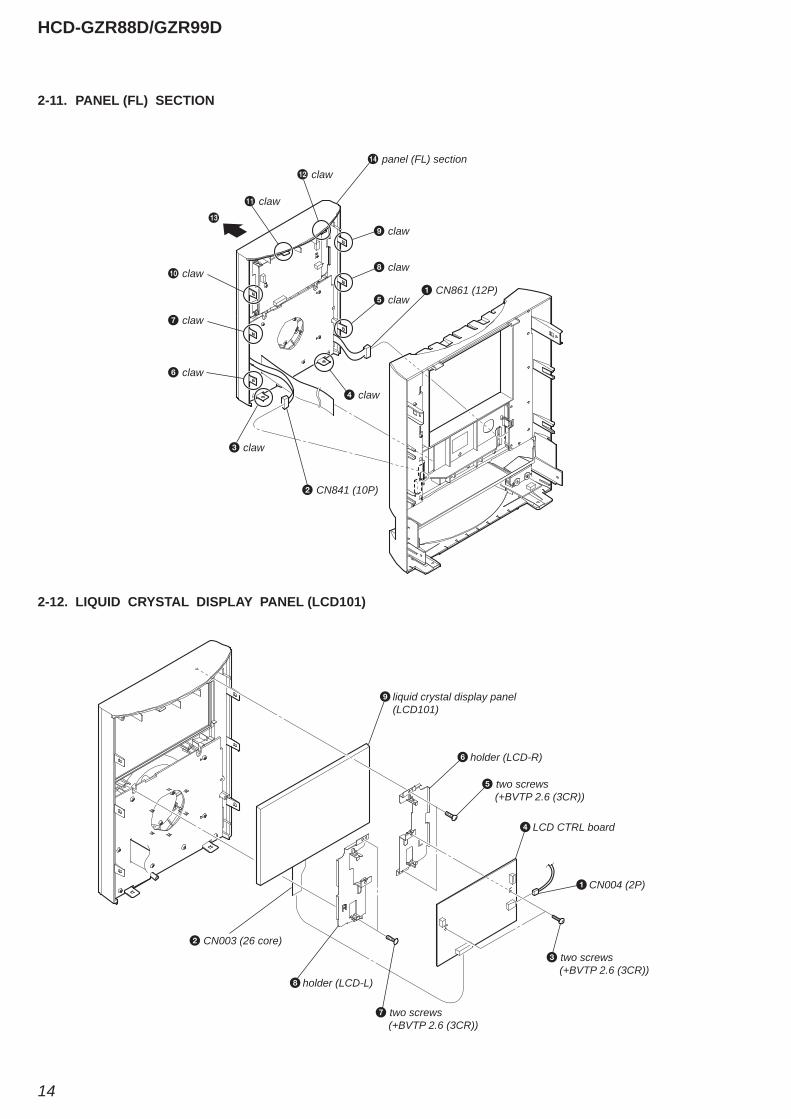
2-12. LIQUID CRYSTAL DISPLAY PANEL (LCD101)
2-11. PANEL (FL) SECTION
1 CN861 (12P)
qf panel (FL) section
2 CN841 (10P)
3 claw
6 claw
7 claw
0 claw
qa claw
qs claw
qd
4 claw
5 claw
8 claw
9 claw
9 liquid crystal display panel (LCD101)
2 CN003 (26 core)
1 CN004 (2P)
4 LCD CTRL board
6 holder (LCD-R)
8 holder (LCD-L)
3 two screws (+BVTP 2.6 (3CR))
5 two screws (+BVTP 2.6 (3CR))
7 two screws (+BVTP 2.6 (3CR))

HCD-GZR88D/GZR99D
15
2-13. FRONT BOARD, VOLUME BOARD
2-14. TC-AMP BOARD (EXCEPT HCD-GZR99D: E2, E51, AR, MX, MODEL)
9 FRONT board
panel (LCD) assy
8 VOLUME board
1 knob (VOL) assy
2 nut3 holder (knob)
4 knob (jog)
5 five screws (+BVTP 2.6 (3CR))
6 four screws (+BVTP 2.6 (3CR))
7 three screws (+BVTP 2.6 (3CR))
1 CN1301 (3P)
2 CN1302 (8P)
4 TC-AMP board
3 three screws (+BVTP 2.6 (3-CR))

HCD-GZR88D/GZR99D
16
2-16. LID (TC-L), LID (TC-R) (EXCEPT HCD-GZR99D: E2, E51, AR, MX, MODEL)
2-15. TAPE MECHANISM DECK (EXCEPT HCD-GZR99D: E2, E51, AR, MX, MODEL)
1 four screws (+BVTP 2.6 (3-CR))
3 three screws (+BVTP 2.6 (3-CR))
4 two screws (+BVTP 2.6 (3-CR))
5 tape mechanism deck
2 shield (top)
1 damper
4 damper
2 spring (TC-R)
5 spring (TC-L)
3 lid (TC-R)
7 panel (top TC)
6 lid (TC-L)

HCD-GZR88D/GZR99D
17
2-17. DRIVER BOARD, SW BOARD
2-18. SENSOR BOARD
6 DRIVER board2 SW board
3 CN704 (2P)
4 CN703 (4P)
7 CN702 (5 core)
5 two screws (+BTTP (M2.6))
1 screw (+BTTP (M2.6))
2 tray
3 belt (table)
5 pulley (table)
8 screw (+BTTP (M2.6))
9 SENSOR board
7 gear (geneva)
0 CN731 (3P)
1 floating screw (+PTPWH M2.6)
6 floating screw (+PTPWH M2.6)
4 floating screw (+PTPWH M2.6)

HCD-GZR88D/GZR99D
18
2-20. MOTOR (LD) BOARD
2-19. MOTOR (TB) BOARD
5 Remove the two solders of motor.
4 MOTOR (TB) board
2 stopper
2 stopper
6 table motor assy (M741)
table assy
3 two screws (+BTTP (M2.6))
1
4 Remove the two solders of motor.3 MOTOR (LD) board
1 belt (loading)
5 loading motor assy (M751)
2 two screws (+BTTP (M2.6))

HCD-GZR88D/GZR99D
19
2-21. CHASSIS
2-22. DMB19 BOARD
1 screw (+BVTP 3 6)
2 two screws (+BVTP 3 8)
3 two screws (+BVTP 3 8)
5 chassis
4
9 two screws (+BVTP 3 8)
0 two screws (+BVTP 3 8)
qs two screws (+BVTP 3 8)
qd screw (+BVTP 2.6 (3CR))
2 wire (flat type)(9 core) (CN1106)
3 wire (flat type)(7 core) (CN1104)
8 wire (flat type)(24 core) (CN101)
qf bracket (DMB)
5 wire (flat type)(7 core) (CN4602)
1 CN1105 (4P)
4 CN1103 (3P)
6 CN601 (9P)
qa DMB19 board
7 CN201 (6P)

HCD-GZR88D/GZR99D
20
2-24. OPTICAL PICK-UP
2-23. BASE UNIT
1 two insulator screws
3 two insulators
4 two insulators
2 two insulator screws
5 optical pick-up
6 holder (310)
1 screw (+PTPWH M2.6)
2 base unit

HCD-GZR88D/GZR99D
21
SECTION 3TEST MODE
[COLD RESET]• The cold reset clears all data including preset data stored in the
RAM to initial conditions. Execute this mode when returning the set to the customer.
Procedure:1. Press the [?/1] button to turn on the system. 2. Press the [x] button, [DISC 3] button and [?/1] button
simultaneously.3. The message “COLD RESET” appears on the liquid crystal
display panel. Then, the liquid crystal display panel becomes blank for a while, and the system is reset.
[COMMON TEST MODE]• This mode is used to check operations of the respective section
of Equalizer level, volume and VACS ON/OFF.
Procedure:• To enter Common Test Mode1. Press the [?/1] button to turn on the system.2. Press the [x] button, [PRESET EQ] button and [DISC 1]
simultaneously.3. The message “VACS0” appears on the liquid crystal display panel.• Check of Equalizer Level1. Press the [EQ BAND/MEMORY] button repeatedly until a
message “ALL EQ MIN” appears on the liquid crystal display panel. GEQ decreases to its minimum.2. Press the [EQ BAND/MEMORY] button repeatedly until a message “ALL EQ MAX” appears on the liquid crystal
display panel. GEQ increases to its maximum.3. Press the [EQ BAND/MEMORY] button repeatedly until a message “ALL EQ FLAT” appears on the liquid crystal
display panel. GEQ is set to fl at.
• Check of Volume1. Press the [DISPLAY] button repeatedly, the sound volume
increases to its maximum and message “VOLUME16” t “VOLUME MAX” appears on the liquid crystal display panel.
2. Press the [OPTIONS] button repeatedly, the sound volume decreases to its minimum and message “VOLUME16” t “VOLUME MIN” appears on the liquid crystal display panel.
• Check of VACS (Variable Attenuation Control System) ON/OFF Select1. Press the [REC TO USB] button repeatedly until a message
“VACS OFF” or “VACS ON” appears on the liquid crystal display panel.
• To release from Common Test Mode1. To release from this mode, press the [?/1] button.2. To cold reset is enforced at the same time.
[AMP TEST MODE]• This mode is used to display the real time VACS level and
check operations of the respective sections of Equalizer band and DBFB ON/OFF.
Procedure:• To enter AMP Test Mode1. Press the [?/1] button to turn on the system.2. Press the [x] button, [GROOVE] button and [DISC 1] button
simultaneously.3. The message “AMP TEST IN” appears of the liquid crystal
display panel.
• Check of VACS Display/AMP Adjustment Select1. Press the [REC TO USB] button repeatedly until a message “V0 0 0” appears on the liquid crystal display panel. “0”
represents VACS level which is triggered by signal level.2. Press the [REC TO USB] button repeatedly until a message “D +6 +2 +4” appears on the liquid crystal display panel.
“+6” represents Equalizer Low level, “+2” represents Equalizer Mid level and “+4” represents Equalizer High level.
• Check of Equalizer Band Select1. Press the [EQ BAND/MEMORY] button repeatedly until a
message “LOW +6 dB” appears on the liquid crystal display panel. EQ Band is set to Low level.
2. Press the [EQ BAND/MEMORY] button repeatedly until a message “MID +2 dB” appears on the liquid crystal display panel. EQ Band is set to Middle level.
3. Press the [EQ BAND/MEMORY] button repeatedly until a message “HIGH +4 dB” appears on the liquid crystal display panel. EQ Band is set to High level.
• Change of Equalizer Band1. Press the [EQ BAND/MEMORY] button repeatedly until a
message “LOW +6 dB” appears on the liquid crystal display panel.
2. When the [OPERATION DIAL] ring is turned clockwise or counterclockwise even slightly, “LOW +6 dB” change to “LOW –8 dB” y “LOW +8 dB” appears on the liquid crystal display panel.
3. Press the [EQ BAND/MEMORY] button repeatedly until a message “MID +2 dB” appears on the liquid crystal display panel.
4. When the [OPERATION DIAL] ring is turned clockwise or counterclockwise even slightly, “MID +2 dB” change to “MID –8 dB” y “MID +8 dB” appears on the liquid crystal display panel.
5. Press the [EQ BAND/MEMORY] button repeatedly until a message “HIGH +4 dB” appears on the liquid crystal display panel.
6. When the [OPERATION DIAL] ring is turned clockwise or counterclockwise even slightly, “HIGH +4 dB” change to “HIGH –8 dB” y “HIGH +8 dB” appears on the liquid crystal display panel.
• Check of DBFB ON/OFF Select1. Press the [OPTIONS] button repeatedly until a message
“DBFB OFF” or “DBFB ON” appears on the liquid crystal display panel.
• To release from AMP Test Mode1. To release from this mode, press the [?/1] button.

HCD-GZR88D/GZR99D
22
[TCM OFFLINE MODE](EXCEPT HCD-GZR99D: E2, E51, AR, MX, MODEL)• This mode prevents the system from tuning off automatically
when TCM is not connected. Therefore, measurements can be done even when TCM is not connected during production.
Procedure:1. Press the [?/1] button to turn off the system and enter the
clock display or demonstration mode.2. Press the [REC TO TAPE] button, [DISC 3] button and [?/1]
button simultaneously. The system will turn on automatically.3. The message “TCM OFFLINE” appears on the liquid crystal
display panel.
• To release from TCM OFFLINE Mode1. To release from this mode, press the [?/1] button.
[PANEL TEST MODE]• This mode is used to check the liquid crystal display panel, LEDs, button, MASTER VOLUME dial, OPERATION DIAL
ring, system software version, DVD lib version, model name and destination.
Procedure:1. Press the [?/1] button to turn on the system.2. Press the [x] button, [DISC 3] button and [DISPLAY] button
simultaneously.3. Power illuminator LEDs and segment in liquid crystal display
panel are lighted up.4. When you want to enter to the system software version
display model, press the [DISC 1] button. The system software version appears on the liquid crystal display panel.
Press the [DISC 1] button again, the DVD lib version appears on the liquid crystal display panel.
5. Press the [DISC 2] button the mode name and destination on the liquid crystal display panel.
6. Press the [DISC 3] button the key encode test mode is activated.
7. In the key encode test mode, the liquid crystal display panel displays “KEY 0 0 0 0 0”.
Each time a button pressed, change the each numbers.
• To release from Panal Test Mode1. To release from this mode, press the [x] button, [DISC 3]
button and [DISPLAY] button simultaneously.
[DVD SHIP MODE (WITHOUT MEMORY CLEAR)]• This mode moves the optical pick-up to the position durable to
vibration. Use this mode when returning the set to the customer after repair.
Procedure:1. Press the [?/1] button to turn on the system.2. Press the [DVD] button, to set the “DVD NO DISC” mode.3. Press the [B] button (HCD-GZR99D: E2, E51, AR, MX model) or [Y] button (Except HCD-GZR99D: E2, E51, AR, MX model) and [?/1] button simultaneously. The system will turn off automatically.4. After the “STANDBY” blinking display fi nishes, a message
“LOCK” appears on the liquid crystal display panel and the DVD ship mode is set.
• To release from DVD Ship Mode1. To release from this mode, press the [?/1] button.
[DVD SHIP MODE (WITH MEMORY CLEAR)]• This mode moves the optical pick-up to the position durable
to vibration and clears all data including preset data stored in the RAM to initial conditions after the power supply is turned off. Use this mode when returning the set to the customer after repair.
Procedure:1. Press the [?/1] button to turn on the system.2. Press the [DVD] button, to set the “DVD NO DISC” mode.3. Press the [TUNING −] button, [DISC 3] button and [?/1]
button simultaneously.4. After the “STANDBY” blinking display fi nishes, a message
“COLD RESET” appears on the liquid crystal display panel and the DVD ship mode is set.
• To release from DVD Ship Mode1. To release from this mode, press the [?/1] button.
[DISC THEFT PREVENTION MODE]• This mode let you lock the disc tray. When this mode is
activated, the disc tray will not open.
Procedure:1. Press the [?/1] button to turn on the system.2. Press the [DVD] button.3. Press the [x] button and [OPEN/CLOSE Z] button
simultaneously and hold down until “LOCKED” or “UNLOCKED” appears on the liquid crystal display panel
(around 5 seconds).
• To release from Disc Theft Prevention Mode1. This mode will not be deselected only by turning the power
off. To exit from the mode, perform the above item 4 again.
[DVD COLOR SYSTEM MODE]• This mode let you change the color system of the video output
from PAL to NTSC or vice-versa.
Procedure:1. Press the [?/1] button to turn on the system.2. Press the [DVD] button.3. Press the [?/1] button to turn off the system.4. Press the [DISPLAY] button to switch the mode the clock display or demonstration mode.5. Press the [X] button and [?/1] button simultaneously. The system will turn on automatically.6. The message “COLOR PAL” or “COLOR NTSC” appears on
the liquid crystal display panel.
• To release from DVD Color System Mode1. Once the color system has been selected, the mode is fi xed
there after. If you wish to change the mode again, perform the above item 4 again.
[DVD FIRMWARE VERSION MODE]• This mode is used to display the DVD fi rmware version.
Procedure:1. Press the [?/1] button to turn on the system.2. Press the [DVD] button.3 Press the [?/1] button to turn off the system and enter the
clock display or demonstration mode.4. Press the [x] button and [?/1] button simultaneously.5. The version of DVD fi rmware appears on the on-screen
display on TV.

HCD-GZR88D/GZR99D
23
• To release from DVD Firmware Version Mode1. To release from this mode, press the [?/1] button.
[MTK REBOOT AVOIDANCE MODE]• This mode is used to display the MTK Reboot Avoidance.
Procedure:1. Press the [?/1] button to turn on the system.2. Press the [DVD] button.3. Press the [DVD] button, [DISPLAY] button and [TUNING +] button simultaneously.
• To release from MTK Reboot Avoidance Mode1. To release from this mode, press the [?/1] button.
[AM TUNER STEP CHAGE]• The step interval of AM channels can be toggled between 9
kHz and 10 kHz.
Procedure:1. Press the [?/1] button to turn on the system.2. Press the [TUNER/BAND] button repeatedly to select the
“AM”.3. Press the [?/1] button to turn off the system.4. Press the [TUNING +] button and [?/1] button
simultaneously. The system will turn on automatically.5. The message “AM 9k STEP” or “AM 10k STEP” appears
on the liquid crystal display panel and thus the channel step change.
[VIDEO/SAT FUNCTION CHANGE]• This mode let you change from VIDEO to SAT and vice-versa.
Procedure:1. Press the [?/1] button to turn on the system.2. Press the [VIDEO/SAT] button.3. Press the [VIDEO/SAT] button and [x] button
simultaneously. The function will change to SAT. Press the same button again
to change from SAT to VIDEO.
[DVD SERVICE MODE]• This mode let you make diagnosis and adjustment easily by
using the remote commander and the TV. The instructions, diagnostic results, etc. are given on the on-screen display.
• TEST DISC LISTBe sure to use the DVD disc that matches the signal standards of your region.• CD YEDS-18 (Part No.: 3-702-101-01) PATD-012 (Part No.: 4-225-203-01)• DVD SL (Single Layer) NTSC : HLX-503 (Part No.: J-6090-069-A) HLX-504 (Part No.: J-6090-088-A) PAL : HLX-506 (Part No.: J-6090-077-A)• DVD DL (Dual Layer) NTSC : HLX-501 (Part No.: J-6090-071-A) HLX-505 (Part No.: J-6090-089-A) PAL : HLX-507 (Part No.: J-6090-078-A)
• Procedure to enter to DVD Service Mode:1. Press the [?/1] button to turn on the system.2. Press the [DVD] button.3. Press the [x] button and [OPEN/CLOSE Z] button
simultaneously and then turn the [MASTER VOLUME] dial clockwise.
4. The message “SERVICE IN” appears on the liquid crystal display panel and the Top Menu of Remocon Diagnosis Menu appears on the on-screen display on the TV. The model name, main unit’s micom version information (IF-con) and DVD fi rmware version information (Syscon) are displayed at the bottom of the on-screen display.
5. To execute each function, press its number by using numeric button on the remote commander.
6. To release from this mode, press the [?/1] button to turn off the system.
• Execute IOP Measurement In order to execute IOP measurement, the following standard
procedures must be followed.
1. From the Top Menu of Remocon Diagnosis Menu, select “2. Drive Manual Operation” by pressing the [2] button on the remote commander. The following screen appears on the on-screen display.
2. Select “3. Manual Adjustment” by pressing the [3] button on the remote commander. The following screen appears on the on-screen display.
Remocon Diagnosis Menu
0. External Chip Check1. Servo Parameter Check2. Drive Manual Operation3. Emergency History4. Version Information
Model NameIF-conSyscon
: STX5DS_E2: Ver. 01.00 (0000): Ver. 1.200
Drive Manual Operation
1. Servo Control2. Track/Layer Jump3. Manual Adjustment4. Mecha test mode5. MIRR time Adjust0. Return to Top Menu
Manual Adjust
1. Track Balance Adjust:2. Track Gain Adjust:3. Focus Balance Adjust:4. Focus Gain Adjust:5. Eg Boost Adjust:6. Iop:7. TRV. Level:8. S curve (FE) Level:9. RFL (PI) Level:0. MIRR Time:
O o Change ValueRETURN Return to previous menu

HCD-GZR88D/GZR99D
24
3. Select “6. Iop:” by pressing the [6] button on the remote commander.
4. Wait until a hexadecimal number appears in the on-screen display as below:
5. Convert data from hexadecimal to decimal by using conversion table.
6. Please fi nd the label on the rear of the BU (Base Unit). The default IOP value is written in the label.7. Subtract between these two values.8. If the remainder is smaller than 93 (decimal), then it is OK. However if the value is higher than 93, then the BU is
defective and need to be change.9. Press the [RETURN] button on the remote commander to
return to previous menu.10. Press the [0] button on the remote commander to return to the
Top Menu of Remocon Diagnosis Menu.11. Press the [?/1] button to turn off the system.
• Check Emergency History To check the emergency history, please follow the following
procedure.
1. From the Top Menu of Remocon Diagnosis Menu, select “3. Emergency History” by pressing the [3] button on the remote commander. The following screen appears on the on-screen display.
2. You can check the total time when the laser is turned on during playback of DVD and CD from the above menu. The maximum time, which can be displayed are 999h 59min.
3. You can check the error code of latest 10 emergency history from the above menu. To view the previous or next page of emergency history, press the [.] button or [>] button
on the remote commander. The error code consists of
• Error Code
The meaning of error code is as below: 01: Communication error (No reply from syscon) 02: Syscon hung up 03: Power OFF request when syscon hung up 19: Thermal shutdown 24: MoveSledHome error 25: Mechanical move error (5 Changer) 26: Mechanical move stack error 30: DC motor adjustment error 31: DPD offset adjustment error 32: TE balance adjustment error 33: TE sensor adjustment error 34: TE loop gain adjustment error 35: FE loop gain adjustment error 36: Bad jitter after adjustment 40: Focus NG 42: Focus layer jump NG 52: Open kick spindle error 51: Spindle stop error 60: Focus on error 61: Seek fail error 62: Read Q data/ID error 70: Lead in data read fail 71: TOC read time out (CD) 80: Can’t buffering 81: Unknown media type
• Parameter of error code This is the detail of error code.
• Time of error code This is the laser time when an error occurred.
To clear the Laser HoursPress the [ DISPLAY] button and then press the [CLEAR] button. The data for both CD and DVD data are reset.
Manual Adjust
1. Track Balance Adjust:2. Track Gain Adjust:3. Focus Balance Adjust:4. Focus Gain Adjust:5. Eg Boost Adjust:6. Iop. ED7. TRV. Level:8. S curve (FE) Level:9. RFL (PI) Level:0. MIRR Time:
O o Change ValueRETURN Return to previous menu
Emg. History Check
1. 01 05 04 04
Laser Hours CD 999h 59minDVD 999h 59min
00 92 46 0000 00 00 00 00 00 23 45
2. 02 02 01 01 00 A9 4B 0000 00 00 00 00 00 23 45
Next Next Page Prev Prev PageO Return to Top Menu
Example of Error code
1. 01 05 04 04 00 92 46 0000 00 00 00 00 00 23 45
Example of Error code
1. 01 05 04 04 00 92 46 0000 00 00 00 00 00 23 45
Example of Error code
1. 01 05 04 04 00 92 46 0000 00 00 00 00 00 23 45
Emg. History Check
1. 01 05 04 04
Laser Hours CD 0h 0minDVD 0h 0min
00 92 46 0000 00 00 00 00 00 23 45
2. 02 02 01 01 00 A9 4B 0000 00 00 00 00 00 23 45
Next Next Page Prev Prev PageO Return to Top Menu

HCD-GZR88D/GZR99D
25
To clear the Emergency HistoryPress the [DVD TOP MENU] button and then press the [CLEAR] button.The error code for all emergency history would be reset.
To clear the Initialize Setup DataPress the [DVD/TUNER MENU] button and then press the [CLEAR] button on the remote commander.
To return to the Top Menu of Remocon Diagnosis MenuPress the [0] button on the remote commander.
• Check Version Information To check the version information, please follow the following
procedure.
1. From the Top Menu of Remocon Diagnosis Menu, select “4. Version Information” by pressing the [4] button on the remote commander. The following screen appears on the on-screen display.
To return to the Top Menu of Remocon Diagnosis Menu,
press the [0] button on the remote commander.
Emg. History Check
1. 00 00 00 00
Laser Hours CD 999h 59minDVD 999h 59min
00 00 00 0000 00 00 00 00 00 00 00
2. 00 00 00 00 00 00 00 0000 00 00 00 00 00 00 00
Next Next Page Prev Prev PageO Return to Top Menu
Version information
O Return to Top Menu
Firm (Main) : Ver. xxxxxFirm (Sub) : xxxxxRISC : xxxxx8032 : xxxxxAudio DSP : xxxxxServo DSP : xxxxx
Emg. History Check
Initialize setup data...
Laser Hours CD 999h 59minDVD 999h 59min
Next Next Page Prev Prev PageO Return to Top Menu

HCD-GZR88D/GZR99D
26
SECTION 4MECHANICAL ADJUSTMENTS
Except HCD-GZR99D: E2, E51, AR, MX Model:Precaution1. Clean the following parts with a denatured alcohol-moistened
swab: record/playback heads pinch rollers erase head rubber belts capstan idlers2. Demagnetize the record/playback head with a head
demagnetizer.3. Do not use a magnetized screwdriver for the adjustments.4. After the adjustments, apply suitable locking compound to
the parts adjusted.5. The adjustments should be performed with the rated power
supply voltage unless otherwise noted.
Torque MeasurementMode Torque meter Meter reading
FWD CQ-102C3.06 N • m to 6.96 N • m
31 to 71 g • cm(0.43 – 0.98 oz • inch)
FWDback tension CQ-102C
0.19 N • m to 0.58 N • m2 to 6 g • cm
(0.02 – 0.08 oz • inch)
REV CQ-102RC3.06 N • m to 6.96 N • m
31 to 71 g • cm(0.43 – 0.98 oz • inch)
REVback tension CQ-102RC
0.19 N • m to 0.58 N • m2 to 6 g • cm
(0.02 – 0.08 oz • inch)
FF/REW CQ-201B6.96 N • m to 14.02 N • m
71 to 143 g • cm(0.98 – 1.99 oz • inch)
FWD tension CQ-403A9.80 N • m
100 g or more(3.53 oz or more)
REV tension CQ-403R9.80 N • m
100 g or more(3.53 oz or more)

HCD-GZR88D/GZR99D
27
Checking Location: DMB19 board (Side A)
SECTION 5ELECTRICAL ADJUSTMENTS
When the optical pick-up assy is replaced, perform the “Execute IOP Measurement”. Execute IOP Measurement (See page 23)
[TEST DISC LIST]Be sure to use the DVD disc that matches the signal standards of your region.• CD YEDS-18 (Part No.: 3-702-101-01) PATD-012 (Part No.: 4-225-203-01)• DVD SL (Single Layer) NTSC : HLX-503 (Part No.: J-6090-069-A) HLX-504 (Part No.: J-6090-088-A) PAL : HLX-506 (Part No.: J-6090-077-A)• DVD DL (Dual Layer) NTSC : HLX-501 (Part No.: J-6090-071-A) HLX-505 (Part No.: J-6090-089-A) PAL : HLX-507 (Part No.: J-6090-078-A)
[RFMON Level Check]Connection:
Procedure:1. Connect an oscilloscope to CN105 pin 6 (RFMON) and
CN105 pin 3 (GND) on the DMB19 board.2. Turn the power on.3. Set the test disc (refer to the TEST DISC LIST) on the tray
and press the [B] button (HCD-GZR99D: E2, E51, AR, MX model) or [Y] button (Except HCD-GZR99D: E2, E51, AR, MX model) to playback.4. Confi rm that oscilloscope waveform is clear and check
RFMON signal level is correct or not.Note: A clear RFMON signal waveform means that the shape
“◊” can be clearly distinguished at the center of the waveform.
FM Tune Level Check
Procedure:1. Turn on the set.2. Input the following signal from signal generator to FM
antenna input directly.
Carrier frequency: A = 87.5 MHz, B = 98 MHz, C = 108 MHz
Deviation : 75 kHzModulation : 1 kHzANT input : 35 dBμ (EMF)
Note: Use 75 ohm coaxial cable to connect signal generator and the set.
You cannot use video cable for checking. Use signal generator whose output impedance is 75 ohm.
3. Set to FM tuner function and tune A, B and C signals.4. Confi rm “TUNED” is lit on the display for A, B and C
signals.
When the selected station signal is received in good condition, “TUNED” is displayed.
DVD SECTION
TUNER SECTION+–
CN105 pin 6 (RFMON)CN105 pin 3 (GND)
oscilloscope
DMB19 board
RFMON signal waveform VOLT/DIV: 200 mVTIME/DIV: 500 nS
level: 0.58 ± 1.23 Vp-p (DVD) 0.57 ± 1.1 Vp-p (CD)
CN105 pin 3(GND)
CN105 pin 6(RFMON)
– DMB19 BOARD (SIDE A) –
IC104
CN105 CN1104
IC101
CN
1103
set
signal generator

HCD-GZR88D/GZR99D
28
Video Level Check (VIDEO BOARD)PurposeThis adjustment is made to satisfy the NTSC standard, and if not adjusted correctly, the brightness will be too large or small.
Procedure:1. Connect oscilloscope to VIDEO OUT jack.2. Load a DVD reference disc playback.3. Check the video signal level is 1.00±0.07Vp-p.
VIDEO SECTIONExcept HCD-GZR99D: E2, E51, AR, MX Model:1. Demagnetize the record/playback head with a head demagnetizer. 2. Do not use a magnetized screwdriver for the adjustments.3. After the adjustments, apply suitable locking compound to
the parts adjust.4. The adjustments should be performed with the rated power
supply voltage unless otherwise noted.5. The adjustments should be performed in the order given in
this service manual. (As a general rule, playback circuit adjustment should be completed before performing recording circuit adjustment.)
6. The adjustments should be performed for both L-CH and R-CH.7. Switches and controls should be set as follows unless
otherwise specifi ed.
• Test Tape
Tape Signal Used forP-4-A063 6.3 kHz, –10 dB Azimuth Adjustment
Record/Playback Head Azimuth Adjustment
DECK BNote: Perform this adjustments for both decks Procedure:1. Mode: Playback
2. Turn the adjustment screw and check output peaks. If the peaks do not match for L-CH and R-CH, turn the adjustment screw so that outputs match within 1dB of peak.
DECK SECTION 0 dB = 0.775V
oscilloscope
set
J1502VIDEO OUT
75 +–
1.00 ± 0.07 Vp-p
(WHITE 100%)
+–
level meter
test tapeP-4-A063(6.3 kHz, –10 dB)
MAIN boardIC101pin wh (L-CH)pin ql (R-CH)
MAIN boardIC101pin t; (GND)
screwposition
L-CHpeak
within1 dB
outputlevel
L-CHpeak
R-CHpeak
within1 dB
screwposition
R-CHpeak

HCD-GZR88D/GZR99D
29
3. Mode: Playback
4. After the adjustments, apply suitable locking compound to the pats adjusted.
Adjustment Location: Record/Playback/Erase Head (Deck B)
oscilloscope
waveform of oscilloscope
in phasegood wrong45° 90° 135° 180°
VR
L
R-CH
L-CH
H
test tapeP-4-A063(6.3 kHz, –10 dB)
MAINboardIC101
pin wh
pin t;
pin ql
reverse
forward

HCD-GZR88D/GZR99D
30
SECTION 6DIAGRAMS
• Circuit Boards Location
VOLUME board
FRONT board
LCD CTRL board
TC-AMP board(except HCD-GZR99D: E2, E51, AR, MX model)
DMB19 board
DRIVER board
SW board
SENSOR board
TRANS-SUB board
VIDEO board
MOTOR (LD) board
MOTOR (TB) board
MIC board
USB-LED board
HP board
LEFT board
RIGHT board
POWER AMP board
MAIN board
TRANS board

HCD-GZR88D/GZR99D
HCD-GZR88D/GZR99D
3131
6-1. BLOCK DIAGRAM – RF/SERVO Section –
: DVD (AUDIO)
: DVD (RF)
: DVD (DIGITAL)
DETECTOR
125
3214
56
RF_CRF_BRF_ARF_D
RF_ERF_F
LD01
MDI1
LD02
MDI2
IC101 (1/2)
DEVICE
COIL
17
15
118
18
16
36 48
43
37 1
Q102 (2/2)
Q102 (1/2)DIODE
(FOR CD)
DIODE(FOR DVD)
DRIVE
4241
BUFFER
35 334 4DRIVE
32
2125
2024
13
128
1162294
IC201
2728 DRIVEMM
4647
FMOFOO
DMOTRO
VREFO
127
FOO
RF
ABCD
FE
CD LD
LIMIT
VR650
VR780
DVD LD
VREFO
VREFO
V2O12VC
VCC
3029 DRIVEMM
23
BUFFER
19202221
40
45
IC501 (1/5)
40 46
91TX TXDFOR
6
1
2
4
5
89RX RXD
V2RFO
42
41
41
88
87
35
43
45
43
44
TRO
FMOFOO
DMOTRO
1013
FMODMO
MUTE123MUTE4

HCD-GZR88D/GZR99D
HCD-GZR88D/GZR99D
3232
DVD SYSTEM PROCESSORIC101 (2/2)
EEPROMIC103
64M SDRAMIC104
A MAINSECTION
C AUDIOSECTION
B MAINSECTION
SF-ROMIC102
AVDD3.3V
VDD1.8V
ASDAT0
ADIN
SDPIF
O-USB-POWER
I-USB-OVER-CURRENT
6 5
SCL
SDA
22-26,29-35
45-49,51-53,56-59,61-64 67,69-74,81-83,85,86
RCLK
38
RCLKRD0 – RD15 RA0 – RA11
RA0 – RA11RD0 – RD15 RWE
16
RWE
RAS
18
RAS
CAS
17
CAS
DQM0
15
DQM0
DQM1
39
DQM1
SCL
SDA
BA0
20
BA0
BA1
21
66 75 77 76 55 6578 80
BA1
2,4,5,7,8,10,11,13,42,44,45,47,48,50,51,53
L IN
A/D CONVERTERIC4601
D/A CONVERTERIC4602
13VINL
CR/RSY/Y/G
SC/CB/B
CVBS
ACLKABCK
ALRCK27
99104102103
106
114115119
120
28
93
10
98
DOUT
7BCKLRCK
6 SCKI
CVBUS OUTCRYCB
1 SDATA4 MCLK2 SCLK3 LRCK
2
14 R-CH
R-CH
8 LOUT
5
OPTICALTRANSMITTER
DVDDIGITAL OUTOPTICAL
VINR
AOUT-L
AOUT-R
IC1502
7
33 3426
WP
EEW
P
5 6
SISC
KSF
_DI
SF_C
K
2
38 3937
SOSF
_DO
1
36
CSSF
_CS
XTALI
XTALO
9
USB DPUSB DM
12
75
3
CN700IC931
+5VREG
IC971
23
73
SYSTEM CONTROLIC501 (2/5)
OVER-CURRENTDETECT
(USB)
2
1
USB DPUSB DM
USB+5V
5
4
1
1
5
IC105
+3.3V REG
+3.3V REG
+1.8V REG
VDD3.3VDVDD5V
18
IC111
45
IC107
RF+3.3V
UNREG10V
X10127MHz
POWERCONTROLQ933,934
: VIDEO
: COMPONENT VIDEO
: AUDIO
: DVD (RF)
: DVD (AUDIO)
: USB
: DVD (DIGITAL)
6-2. BLOCK DIAGRAM – VIDEO Section –
(Page 33)
(Page 34)
(Page 33)

HCD-GZR88D/GZR99D
HCD-GZR88D/GZR99D
3333
VIDEOSECTION B
VIDEOSECTION A
DISPLAY/POWERSECTION
E
AUDIOSECTIOND1
21
3
2
9
22
15162826272931
45
4689
T1301
HRPE901REC/PB/ERASE
HEAD(DECK B)
HP901PB
HEAD(DECK A)
REC/PBHEAD
TAPE MECHANISMDECK BLOCK
ERASEHEAD
A-PHOTOB-PHOTO
B-REC-REVA-HALF
B-HALFB-REC-FWD
CAP M+
R-CH
EXCEPT E2,E51,AR,MX MODEL
R-CH
R-CH
L-CH
R-CH
L-CH
2
43
42
44
37
3
5785
86
58
4
10B A
11
143
21
20
18
16
6
10
12
9
14
3 13
59
87
23
26
9
27
28
36
18
17
19
14
6
10
8
7
6
5
B-SOL
A-SOL
LOUT
VIDEO-L
TUNER-L
DMB-L
TAPE REC/PB AMP,SOUND CONTROLIC101
SYSTEM CONTROLIC501 (3/5)
RECAL
SWOUT
OUTL
BB1L
BB2L
RECA L
MIC_SCORE
SW OUT
FL OUT
DBFBD417
HP DET
SA2
DATA
CLK
MIC
O-AUDIO-IC-DATAO-AUDIO-IC-CLKI-TU-DOO-TU-DIO-TU-CLKO-TU-CEI-TU-TUNE
O-TC-REC-MUTE
O-TC-REC/PB-SW
O-TC-REC-BIAS
O-TC-CAPM-CNT
O-TC-B-TRIGO-VIDEO-MUTE
88O-VIDEO-I/P
I-ILLUMINATION
I-VACS
O-VIDEO-SW-AI-MIC/HP-DET
O-VIDEO-SW-B
O-FRONT-MUTE
O-TC-A-TRIG
TC-A-SHUTTC-B-SHUTO-TC-REC-REVI-TC-STAT
TAPE-L
RECBL
CAPSTAN/REEL MOTOR
CONTROLQ631,634
SOLENOID ACONTROLQ633,636
SOLENOID BCONTROLQ632,635
BIAS OSCQ1453
MUTEQ1305
MUTEQ1401,1403
MUTEQ1405
MUTEQ1303
MUTEQ1301
BUFFERQ815
MIC 1LEVELMIC AMP
IC700MIC AMP
IC701 (2/2)
MIC AMPIC701 (1/2)
RV700
3 1
3 1
5 7
MIC 2LEVEL
RV701
MIX IN MIX OUT
MIC ECHO AMPIC720
ECHO VOL
ECHOLEVEL
RV720
REC/PBSWITCHQ1408
FL MUTEQ242
FRONTSPEAKER
MUTEQ691
DBFB FEEDBACK AMP
Q128
VACSCONTROLQ101,102
CVBUS OUT
Y
CB
CR
CVBS IN
D3
LCD VIDEO
D1
COMPONENT VIDEO AMPIC1501
VIDEO SELECTORIC1500
Y-IN
CY-IN
CB-IN
I/P
CR-IN
COM
Y OUT
23CVBS OUT
MUTE1 MUTE2
CY OUT
CB OUT
CR OUT
REC MUTECONTROL
Q1410
MUTECONTROL
Q1407
REC MUTEQ1409
PB AMPIC1301
REC AMPIC1401
31
3 1
Q1454,1455
+9V
74755
60
FM 75COAXIAL
AM
J221
TM901
R-CH
L
R
R-CH
+9VDO
DI
CL
CETUNE
RCH
LCH
+9V
DO
DI
CLK
CETUNED
AUDIO IN -2
-1
ANTENNA
MIC 1J700
MIC 2J701
VIDEO/SAT
VIDEOOUT
Y-3
-2
-1PB/CB
PR/CR
J1502
COMPONENTVIDEO OUT
J1501
VIDEO/SAT
VIDEO IN
J1500 12
S P
R-CH L-CH
: TAPE PLAY (DECK B)
: TUNER
: TAPE PLAY (DECK A)
: TAPE REC (DECK B)
: AUDIO
AE2 : 120V AC E E51 : C P AR : A MX : M
: VIDEO
: COMPONENT VIDEO
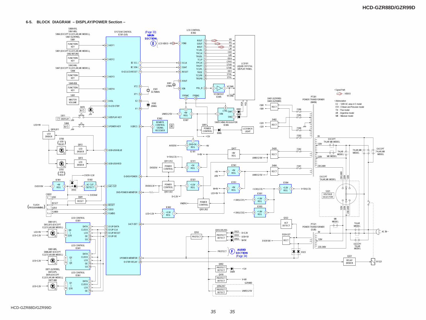
6-3. BLOCK DIAGRAM – MAIN Section –
(Page 35)
(Page 32)
(Page 34)
(Page 32)

HCD-GZR88D/GZR99D
HCD-GZR88D/GZR99D
3434
MAINSECTION D
DISPLAY/POWERSECTION
F
VIDEOSECTIONC
+
–
9
L+
–
+
–
L+
–
+
–
L+
–
+
–
+
–
9
9
6-4. BLOCK DIAGRAM – AUDIO Section –
(Page 32)
(Page 35)
(Page 33)
HCD-GZR88D/GZR99D
HCD-GZR88D/GZR99D
3535
( )
( )
( )
FLASHPROGRAMMING
_/1
_/1
91XT2
92XT1
13 I-AC-CUT3
IC901
LED CONTROLIC801
CN5912
4
51
VDD
RESET
SI/SOFLMD0
+4VREGEVER10V
LED+9V
EVER+3.3V
EVER4V
1
5
1
IC181
IC862
FPPWC FPBIAS
IC911
DVD+5VREG4
REMOTECONTROL
SIGNALRECEIVER
2
1
IC682
AC CUTDETECT2
Q681
90 RESET
D870
S868
DISPLAYS811
65 I-KEY1
X50132.768kHz
94X2
95X1
81I-SIRCS
1IIC SCL
24O-DVD-POWER
40I-ACF-DET
55DVD-POWER-MONITOR
X50220MHz
6I
16
Q0 |
Q10
+58V
F306–58V
AC IN ~
PT301POWER TRANSFORMER
(MAIN)
PT321POWER TRANSFORMER
(SUB)
SYSTEM CONTROLIC501 (5/5)
80 USB-USB-RED
FUNCTIONKEY
S808-810,S861-865,
S866 (EXCEPT E2,E51,AR,MX MODEL),S867 (GZR99D),
S881
64 I-KEY2FUNCTIONKEY
S801 (EXCEPT E2,E51,AR,MX MODEL),S802-807,892
63 I-KEY3
63 SCLK
3 YIN0
X00127MHz
54 XOUT
55 XIN
2IIC SDA 62 SDAT
11O-GC/LCD-RESET 56 RESETFUNCTION
KEY
62 I-KEY4FUNCTIONKEY
61 I-VOL
68 O-LED-STBY
79 USB-USB-BLUE
82 I-DISPLAY-KEY
83 I-POWER-KEY
MASTERVOLUME
S842-846,S847 (EXCEPT E2,E51,AR,MX MODEL),
S848
S849-858
S891
RELAYDRIVER
Q321
VOLTAGESELECTOR
S321
TH,ARMODEL
MXMODEL
TH,ARMODEL
TH,AR,MXMODEL
EXCEPTTH,AR MX MODEL
EXCEPT TH,AR,MX MODEL
MX MODEL
EXCEPTTH,AR,MX MODEL
EXCEPTTH,ARMODEL
RY321
0V
120V
220-240V
Q810,811
D801-811,D812,813 (EXCEPT
E2,E51,AR,MX MODEL)
D881-885,D886,887 (EXCEPT
E2,E51,AR,MX MODEL)
D871 (GZR99D),D872-875,
D876 (EXCEPTE2,E51,AR,MX MODEL),
D877-880
LEDDRIVER
LEDDRIVER
Q812USBBLUE
D700
USBRED
D701
D401 (GZR99D)D403 (GZR88D)
LEDDRIVER
Q813
RESET
89 SI/SO93 FLMDO
72 O-S/P-DATA70 O-S/P-CLK69 O-S/P-RESET71 O-S/P-OE
3DATA
LED+9V4CLOCK5LCK19OE18SO
LED CONTROLIC841
9I
15
3DATA
LED+3.3V4CLOCK5LCK19OE18SO
LED CONTROLIC861
7I
16
Q1 |
Q10
Q3 | Q9
3DATA
LED+3.3V
LED+3.3V
4CLOCK5LCK19OE
F305
D402
F303
F304
RECT
F302D420
RECT
+32V–32V
RECT
AVDD5V
1+5VREG3DVDD5V
V+5V(LCD)
+9V
+12V
2
5
IC007
VCOM OUTIC005
CTRL+9VREG1
38
SWITCHING REGULATORIC006
D006
D005
D001
VINSW1
VGH
VGL
1SW22
15 10
UNREG15V
F301
0V
120V
120V
220V
220V
120V
230-
240V
230-
240V
220V
V+5V(LCD)
230-240VD404
RECT
D323
D324-327
Q322
RECT
+9V
V+8V
A9V
M+9V
LED+9V
EVER10V
UNREG10V
UNREG15V
IC921
Q921,922
1+3.3VREG2
IC961
1+9VREG3
USB+5VM+9V
+12V
V+8V
UNREG15V
D+3.3V
PROTECT
GZR88D
D933D923
D953
D009
Q552Q925,935,955
D553
POWERCONTROL
Q911,912
POWERCONTROL
DVDD3.3V
Q951,952
POWERCONTROL
+8V REG
VM(9V)
D+3.3V
52I-POWER-MONITOR49O-STBY-RELAY
LCD CONTROLIC002
LCD101LIQUID CRYSTALDISPLAY PANEL
PROTECT PROTECTDETECT
ACFDETECT
IC951
Q417
1+9VREG2
+1.8V(LCD1)
+1.8V(LCD2)
IC001
5+1.8VREG4
IC003
5+1.8VREG4
+3.3V(LCD)
IC004
5+3.3VREG4
LED+3.3V
IC802
1+3.3VREG3
73ROUT VR
74GOUT VG
75BOUT VB
14TCLRL L/R
16TRCLK CKV
17TRUDL U/D
21TCLP OEH
22FPCLK CPH1
25TRSPT STVR
26TCSPL STHR
27TROE OEV
28TCSPR STHL
29TRSPB STVL
20 2 1POL_B VCOM1
VCOM2
AUDIOSECTIONF
LCD VIDEO
MAINSECTION
E
Q956,957PROTECTDETECT
Q418PROTECTDETECT
Q002PROTECTDETECT
POWERCONTROL
Q001LCD BACK
LIGHT
AE2 120V AC E E51 C P TH T AR A MX M
S P: VIDEO
6-5. BLOCK DIAGRAM – DISPLAY/POWER Section –
(Page 33)
(Page 34)

HCD-GZR88D/GZR99D
HCD-GZR88D/GZR99D
3636
For Schematic Diagrams.Note:• All capacitors are in μF unless otherwise noted. (p: pF) 50
WV or less are not indicated except for electrolytics and tantalums.
• All resistors are in Ω and 1/4 W or less unless otherwise specifi ed.
• 2 : Nonfl ammable resistor.• C : Panel designation.
THIS NOTE IS COMMON FOR PRINTED WIRING BOARDS AND SCHEMATIC DIAGRAMS.(In addition to this, the necessary note is printed in each block.)
• A : B+ Line.• B : B– Line.• Voltages and waveforms are dc with respect to ground
under no-signal (detuned) conditions. no mark : FM * : Impossible to measure• Voltages are taken with VOM (Input impedance 10 MΩ). Voltage variations may be noted due to normal production
tolerances.• Waveforms are taken with a oscilloscope. Voltage variations may be noted due to normal production
tolerances.• Circled numbers refer to waveforms.• Signal path. F : AUDIO f : TUNER L : VIDEO g : COMPONENT VIDEO E : TAPE PLAY (DECK A) d : TAPE PLAY (DECK B) G : TAPE REC (DECK B) J : DVD (AUDIO) c : DVD (RF) I : DVD (DIGITAL) N : USB• Abbreviation AR : Argentina model E2 : 120V AC area in E model E3 : 240V AC area in E model E4 : 110 – 120V/220 – 240V AC area in E model E12 : 220 – 240V AC area in E model E15 : Iran model E51 : Chilean and Peruvian model MX : Mexican model PH : Philippines model SP : Singapore model TH : Thai model
For Printed Wiring Boards.Note:• X : Parts extracted from the component side.• Y : Parts extracted from the conductor side.• : Pattern from the side which enables seeing. (The other layers' patterns are not indicated.)
• Abbreviation AR : Argentina model E2 : 120V AC area in E model E3 : 240V AC area in E model E4 : 110 – 120V/220 – 240V AC area in E model E12 : 220 – 240V AC area in E model E15 : Iran model E51 : Chilean and Peruvian model MX : Mexican model PH : Philippines model SP : Singapore model TH : Thai model
Note: The components identifi ed by mark 0 or dotted line with mark 0 are critical for safety.
Replace only with part number specifi ed.
Caution:Pattern face side:(Conductor Side)Parts face side: (Component Side)
Parts on the pattern face side seen from the pattern face are indicated.Parts on the parts face side seen from the parts face are indicated.
UNLEADED SOLDERBoards requiring use of unleaded solder are printed with the lead-free mark (LF) indicating the solder contains no lead.(Caution: Some printed circuit boards may not come printed with
the lead free mark due to their particular size)
: LEAD FREE MARKUnleaded solder has the following characteristics.• Unleaded solder melts at a temperature about 40 °C higher
than ordinary solder. Ordinary soldering irons can be used but the iron tip has to be
applied to the solder joint for a slightly longer time. Soldering irons using a temperature regulator should be set to
about 350 °C.Caution: The printed pattern (copper foil) may peel away if
the heated tip is applied for too long, so be careful!• Strong viscosity Unleaded solder is more viscous (sticky, less prone to fl ow)
than ordinary solder so use caution not to let solder bridges occur such as on IC pins, etc.
• Usable with ordinary solder It is best to use only unleaded solder but unleaded solder may
also be added to ordinary solder.
• Waveforms
– DMB19 Board –
– MAIN Board – – LCD CTRL Board –
2 IC101 ol (CVBS)
1 IC101 9 (XTALI)
3 IC101 <z/x (SY/Y/G)
500 mV/DIV, 20 μsec/DIV
500 mV/DIV, 20 nsec/DIV
500 mV/DIV, 20 μsec/DIV
5 IC101 <z/v (CR/R)
4 IC101 <z/c (SC/CB/B)
6 IC101 <zxb (RFIP)
500 mV/DIV, 20 μsec/DIV
500 mV/DIV, 20 μsec/DIV
200 mV/DIV, 100 nsec/DIV
0.9 Vp-p
27 MHz
1 Vp-pH
0.3 Vp-pH
0.5 Vp-pH
0.5 Vp-pH
700 mVp-p
2 IC501 og (X1)
1 IC501 os (XT1)
0.5 V/DIV, 20 nsec/DIV
0.5 V/DIV, 20 μsec/DIV
1.6 Vp-p
32.768 kHz
0.7 Vp-p
20 MHz
1 IC002 tf (XOUT)
1 V/DIV, 50 nsec/DIV
2.2 Vp-p
27 MHz

HCD-GZR88D/GZR99D
HCD-GZR88D/GZR99D
3737
1
A
B
C
D
E
F
G
H
2 3 4 5 6 7 8 9 10 11 12 13 14
(DISC TRAY ADDRESS DETECT)
1
2
1
4
3
9
19
1
4
12
1 2
B C E
(TABLE)(LOADING)
CN751
CLOSE OPEN
IC731
CN731
CN741
M741
CN74
2
CN72
1M751
MAINBOARDCN641
A
C715
C731
C735
C736
R701
R711
R731
R721
R722
R723
R736
R732
R733
R734
D701
D711
C751
IC71
2
IC70
1
CN704
C737
R713
R712
C741
R702
JW702
JW703
JW704
JW705
JW706
JW707
JW70
8
JW711CN703
CN702 CN705
R751
C752
JW712
JW701
JW70
9
JW710
JW713
JW714
RE701
RE701
CN711
CN70
1
Q731
S751(OPEN/CLOSE DETECT)
S751
6-6. PRINTED WIRING BOARDS – DRIVER Section – • See page 30 for Circuit Boards Location.
(Page 45)
• : Uses unleaded solder.

HCD-GZR88D/GZR99D
HCD-GZR88D/GZR99D
38
IC B/D
IC B/D
R751
C752CN705
CN704CN721
CN751
C751
IC701
IC712
R701
R713
R711
R723 R721R722
C735C736C737
R736
R733R731
C731Q731
C741
CN703
IC731CN731 CN741
CN742
C715
R702
R712
R732R734
D711
M751
M741
S751
CN701
D701
CN702
CN711
RE701
38
6-7. SCHEMATIC DIAGRAM – DRIVER Section – • See page 68 for IC Block Diagrams.
(Page 46)

HCD-GZR88D/GZR99D
HCD-GZR88D/GZR99D
3939
1
A
B
C
D
E
F
G
H
I
234567891011
IC101
IC10
4
1 719
1 3
1
1
2854
271
3233
96128 97
6564
91 4
224
123
16
17
16
C1504C1510
CN20
1
RED
GRY
GRY
GRY
GRY
GRY
R111
0
CN4602
R230
R1114
R231
R232
CN601
R1121R1123
C460
8
R246
R247
JL001
JL002
JL003
JL004
JL005JL006
C216
JL007
C217
C218
CL105
CL106
C602
CL107
C603
CL108
C604
CL109
JL20
1JL
202
JL203
JL010
C220
JL205
JL012
JL206
JL014
R460
1
JL016JL017
C611
JL210
JL211
JL212
JL213JL214
JL215
R1151R1152
C620
C621
C622
C623
FB1264
FB12
65
R116
8
D001
D002
D003
D004
FB1284
FB1285FB1286
R1187
RB10
5ET001 RB
106
ET002
RB10
7
ET003
RB10
8
ET004
RB11
1
RB11
2 RB11
3
RB11
4
RB11
5
JL12
01
JL1202
JL12
03JL
1204
JL12
05
JL1206JL1207
JL1208
JL1209
JL1210
JL1211JL1212JL1213
JL1214JL1216
JL1218JL1220
R102
R103
R107
R114
CN10
1
CN10
5
C101
C105
R142
C106
X101
C112
C113
C118
R156
C124
CL20
6CL207
CL208
JL113
JL114
JL115
CL213
R1249
R125
7R1
258
R125
9R1
260
R1263
FB12
66
C152
C153
R126
9
R191
R192
R193
R195
R197
R198
R1271R1270
C160
R127
6
R1277
FB4835FB4836
R128
1
R128
2
R128
3
JL1101
JL1102 JL1105JL1106
JL1107JL1108
C190
JL1110
JL1111JL1112 JL1113
JL1114
JL1115
JL1116
JL1117
CL1138
JL1118
CL1139
JL1119
CL11
40
JL1120
CL1141
JL1121
CL1142
JL1122
JL1123
JL1124
CL1146
CL1147CL1148
CL1149
CN1103
CN11
04
CN1105CN1106
CL11
50
CL1151
CL1152
OPTICALPICK-UPBLOCK
DMB19 BOARD (SIDE A)
12(12)1-878-221-
FVIDEOBOARDCN1500
BMAIN BOARD
CN504
G
VIDEO BOARDCN1503
C
MAIN BOARDCN191
D
MAIN BOARDCN951
EMIC BOARD
CN706
FORLINE-JIG
JL11
31
JL11
32
JL11
33
JL11
34
6-8. PRINTED WIRING BOARD – DMB19 Section (1/2) – • See page 30 for Circuit Boards Location.
(Page 45) (Page 53)
(Page 53)
(Page 45)
(Page 49) (Page 45)
• : Uses unleaded solder.

HCD-GZR88D/GZR99D
HCD-GZR88D/GZR99D
4040
6-9. PRINTED WIRING BOARD – DMB19 Section (2/2) – • See page 30 for Circuit Boards Location. • : Uses unleaded solder.
1
A
B
C
D
E
F
G
H
I
2 3 4 5 6 7 8 9 10 11
IC46
01
IC4602
IC105
IC111
IC10
3
IC10
2
IC107
IC201
1
1213
48
2425
3637
58 1
14
85
4
C1E1B1B2
E2C2
D1G2S2G1D2 S1
FB60
6
FB607
R210
FB608
FB609
C1505
R212
C1506
R213
C1507
R214
R215
R216
R219R1101
C1512
C1513
R220
R221
R223
C1130
R224
R225
R226
R233R234
C460
2 C460
3
C4606
C203
C205
C206
C208
R112
9
C209
C210
C211
C212
C213
C214
C215
C219
R256
C462
2
C4623
C607
C221
C4626
C222
C224
R460
2
C610
R460
5
R460
6
R4608
R4609
R115
0
C233R4611
17
14
8 5
1 4
8 5
5
1 3
4
5
1 3
4
1 4
8
FB12
67FB
1268
C630
R1177
R117
8
Q101
D006
Q102
E C B Q103R4
833
R1184
R4834
R483
5
R119
1
R1192R1
193 R119
4
FB106
FB10
8
FB10
9
R101
FB11
2
R108
R109
R110
R111
R112R113R115
R116 R117
R118R120R121
R122
R123 R124
R125
R133
R135
R136
R521
C102
C108
C111
R151
C115
C116
C119
C502
CL201
CL202
CL204
C125
CL205
C126
C127
R1252
R125
3
R1255
C144
C145
C146
C149
R126
1
R126
2
C150
C151
C154
C155
C156
R1278R1279
C168
C169R128
0
C172
C175
C179C180
C181
C182
C183
C184
C186
C188
C191
C192
C193
C195
C197
C198
C199
FL603
R204
R205
R206
R207
R208
R209
FB603
12(12)1-878-221-
DMB19 BOARD (SIDE B)

HCD-GZR88D/GZR99D
HCD-GZR88D/GZR99D
4141
8 10
I
F
B
63
D
7
E
9
G
C
21
H
1154
A(3/4)
DMB193BOARD
DMB19BOARD
(3/4)4
DMB19BOARD
(3/4)5
MICBOARDCN706
E
DMB19BOARD
(4/4)6
BOARD(2/4)
1DMB19
DMB19
(2/4)BOARD2
IC B/D IC B/D IC B/D
0
0
0
0
01.3
1.3
0
1.6 1.6
3.2
0 0
5 3.3
3.2
1.3
3.2
3.2
0.5
1.8
5 3.3
3.2
1.3
3.2
3.3
3.2
3.2 0.4
0
3.2
3.2
3.2
0
0
3.2
(1/4)DMB19 BOARD
IC107
IC111
IC105
IC103
IC102
123456
6PCN105
TXDRXDGND
+3.3VV2REFORFMON
47kR124
0.01C192
5 4
321TK11
133C
SCL-
GIC
105
+3.3V REG
CONT
GND
NOIS
EVO
UTVIN
0.5%22
R112
2.7kR1110
100kR114
100R109
0.01C113
0.5%22
R115
100R101
10kR107
10V47
C105
1kR1
93
0.22C195
47kR117
C1820.22
1kR116
0.01C101
22R121
C1840.01
10V47
C112
1MR108
123456789
101112131415161718192021222324
CN10124P
GND (LD)LD (650)
NCNCPD
LD (780)VR (650)VR (780)
NCVOE/E+G
VCCVC
GND (PDIC)VOF/F+H
VOB/BVOA/A
RF(LO:DVD.HI:CD)MSW
VOD/DVOC/C
TRK-TRK+FCS+FCS-
0.01C106
0.5%22
R113
5 4
321TK11
133C
SCL-
GIC
107
+3.3V REG
CONT
GND
NOIS
EVO
UTVIN
100R123
1kR1
91
47kR110
0.22C193
22R118
RT1N241C-TP-1Q103
MEDIA SWITCH CONTROL
22R120
100kR1129
100R111
D1G2
S2D2G1
S1
UM6K1N-TNQ101
MEDIA SWITCH CONTROL
Q102QST8TR
LASER DRIVER CONTROL
JL1101JL1102
JL1105JL1106JL1107JL1108
JL1110JL1111JL1112JL1113JL1114JL1115JL1116JL1117JL1118JL1119JL1120JL1121JL1122JL1123JL1124
CL106
CL107
REG01
TRK-TRK+FCS+FCS-
REG02
IOPIOPMON
VREFO
RF+3.3VDVDD5V
DGND
C188470p
1C198
1C1
83
1kR1
178
DGND
C1860.22
R15110k
FB112
0.01C1130
10k
R135
R1020
87
654
32
1
87
654
32
1
S-24CS16A0I-J8T1GIC103
EEPROM
A0
A1
A2
GND SDA
SCL
WE
VCC
IC102
SF-ROMMX25L3205DM2I-12G
_CS
SO
_W
GND SI
SCK
_HOLD
VCC
USB+5V
JL1133JL1132
JL1134
JL1131
DVDD3.3V
CL105V2REFO
0R1192
R12520
0R1253
87
65 4
32
1
MM1661JHBEIC111
+1.8V REG
VO
NC
GND
CNCONT
NC
NC
VIN
FB109
C15070.1
USBGND
1234
4PCN1105
GNDD+D-
VBUS
CL1152
R12800
DGND
DVDD5V
1
2
3
4BUS1
5
678
9
10
111213
14
15
16171819
2122
23
24
BUS2
0.1C102
DVD_LD
CD_LD
CD_LDDVD_LD
VOE
VOFVOBVOA
VODVOCTRK-TRK+FCS+FCS-
TRK-TRK+FCS+FCS-
USBMUSBP
(1/2)
PICK-UPOPTICAL
BLOCK
LINE-JIG)( FOR
6-10. SCHEMATIC DIAGRAM – DMB19 Section (1/4) – • See page 68 for IC Block Diagrams.
(Page 42)
(Page 42)
(Page 43)
(Page 43)
(Page 43)
(Page 44)
(Page 50)

HCD-GZR88D/GZR99D
HCD-GZR88D/GZR99D
4242
F
2 1514
B
H
5
A
C
I
E
114
J
10
G
133 71 986 12
D
DMB19
(1/4)BOARD 1
7BOARDDMB19
(3/4)
BOARD(1/4)
2DMB19
6
1
5 4 3 2
CN1500
VIDEOF BOARD
(3/4)
DMB198 BOARD
GVIDEO
BOARDCN1503
10(4/4)
DMB19BOARD
BOARD(3/4)
DMB19
(1/3)BOARD
MAIN
BCN504
9
1.4 2.6
1 1 1.8
3.3
3.3
0 1.7
0 0.8
3.2
1.7
2.2
1 3.3
03.3
0 0.9
3.3
0 0.3
3.3
3.3
0.3
1.3
03.30.21.6
3.21.83.13.22.20.313.210.200.9
2.83.233.20.30.40.30.20.10.13.20.11.62.9
3.2
3.2
3.2
0.4 0 0 0
3.2
0.1
3.2 0
0.5 1
0.9
0.6
3.2
0.1
0.1
1.1
1.8
2.6 1 0
1.5
1.2
0.9
0.2 1
0.5
222222
1.83.30.80.8
21.41.40.60.63.33.33.3
1.41.4
3.30
1.41.4
3.300
3.2
0.81.8
0.3
0.4
0.3
0.2
0.1
0.1
0.1
3.1
1.6
2.9
0.5
3.2
1
0.2
0.9
1.2
3.2
1.5
0
1
3.2
0.3
1
1
0.2
0
0.9
2.8
0
3.2
3
3.2
2.6
3.2
1.1
0.1
0.1
3.2
0.6
0.9
1
0.5
3.2
1.2
3.2
IC101
IC104
3.3kR1151
0.1C179
100
R156
4700pC199
0.1C116
1C1
24
3.3kR1150
0.1C115
3.3kR1152
10V100
C190
0.01
C160
0.1C191
15kR136
0.1C197
0.01C144
0.1C180
C169 0.1
JL1207
JL1205JL1204JL1203JL1202JL1201
DGNDDVDD3.3V
TROFOO
SPFG
TSD_M
DMO
ALRCK
FMO
ABCKACLK
ASDATA0
FB10
8
0.1C181
LIMITSW
22R1114
0R133
0.5%
R197
150
0.5%
R195150
0.5%
R192150
0.5%
R198150
MUTE4MUTE123
ADIN
R1187220
100kR142
12p
C152
12p
C153
CL11
41
100R1184
0.1C155
0.5%560
R1101
0R11210R1123
0.5%5.1kR103
27MH
zX1
01
0R1177
220p
C150
4
JL113JL114JL115
330R1168
0.5%
C125 0.1
0R1
191
0R1
194
0R1
193
1C1
27
12
34
56
78
910
1112
1314
1516
1718
1920
2122
2324
2526
2728
2930
3132
33 34 35 36 37 38 39 40 41 42 43 44 45 46 47 48 49 50 51 52 53 54 55 56 57 58 59 60 61 62 63 64
6566
6768
6970
7172
7374
7576
7778
7980
8182
8384
8586
8788
8990
9192
9394
9596
979899100101102103104105106107108109110111112113114115116117118119120121122123124125126127128
CXD9971RIC101
RF_ARF_BRF_CRF_DRF_ERF_FAVDD18_2AVDD33_1XTALIXTALOAGND33V20V14/VREFOREXTMDI1MDI2LDO1LDO2AVDD33_2DMOFMOMUTE4MSWTROFOOEEWPUSB_DPUSB_DMVDD33_USBVSS33_USBPAD_VRTVDD18_USB
SCL
SDA
IFSD
ISF
_CS#
SF_D
OSF
_DI
SF_C
KIF
SCK
IFSD
OIC
EPR
ST#
IR RD0
RD1
RD2
RD3
RD4
DVDD
33RD
5RD
6RD
7DV
DD18
DQM0
RD15
RD14
RD13
RD12
DVSS
33RD
11RD
10RD
9RD
8
DQM1RCLKRA11
DVDD33RA9RA8RA7RA6RA5RA4
RWE#CAS#RAS#
BA0DVSS18
BA1RA10
RA0RA1
DVDD33RA2RA3
IFBSYIFCS#
RXDVDD18
TXXMAMUTE
SPDIFTSDM
DACVDDCVREF
FSDA
CVSS
CCV
BSDA
CVDD
BDA
CVDD
ASY
/Y/G
SC/C
B/B
CR/R
AADV
SSAD
INMU
TE12
3LI
MITS
WAA
DVDD
APLL
VDD
APLL
CAP
ADAC
VSS2
ADAC
VSS1
ACLK
ABCK
MUTE
123
AVCM
LIMI
TSW
ALRC
KAS
DATA
0AD
ACVD
D1AD
ACVD
D2AV
DD18
_1AG
ND18
RFIP
OPOU
TIO
PMON
SPFG
CL108 CL109
10kR122
10kR125
0.01C1505
0.1C111
0.01C156
0.01C151
0.01C175
0.01C150
0.01C149
0.01C172
C168 0.11
C146
0.01
C145
0.1
C154
CL11
42
CL11
46CL
1147
CL11
40
16V10C118
10C119
RB10633X4
RB10533X4
4748
49
8
5051
5253
54 12
34
56
7
4142
4344
4546
1413
1211
109
3440
3536
3738
39 1615
1718
1920
21
28 27
2930
3132
33
2625
2423
22
EM638165TS-6GIC104
64M SDRAM
VDD
DG0
VDDQ
DQ1
DQ2
VSSQ
DQ3
DQ4
VDDQ
DQ5
DQ6
VSSQ
DQ7
VDD
LDQM
WE
CAS
RAS
CS
BA0
BA1
A10/AP
A0
A1
A2
A3
VDDVSS
A4
A5
A6
A7
A8
A9
A11
NC
CLKE
CLK
UDQM
NC
VSS
DQ8
VDDQ
DQ9
DQ10
VSSQ
DQ11
DQ12
VDDQ
DQ13
DQ14
VSSQ
DQ15
VSS
RB10833X4
RB10733X4
RB11133X4
CL1138CL1139
1500
pC1
08
10C1
26
FB106
1000pC1506
R12491k
0R1
255
123
3PCN1103
+3.3VSPDIFDGND
1234567
7PCN1104
CRDGNDCBDGNDYDGNDCVBUS OUT
CL11
48
CL11
49CL1150CL1151
0.1C1510
R1257 0R1258 0R1259 0R1260 0
10k
R126
1
10k
R126
2
JL1214JL1216JL1218JL1220
0R1263
RB11233X4
RB11433X4
RB11533X4
RB11333X4
100
R126
9
JL1206
0.1C1512
0.1C1513
123456789
9PCN1106
XIFCSXIBSYXSYSRSTIFSDIIFSDODGNDIFSCKNCNC
R1270 0R1271 0
R1276 0R1277 100
R127
810
kR1
279
10k
FB12
67FB
1268
FB1264FB1265FB1266
100
R128
1
22R1
282
R128
310
0
FB1285
FB1286
FB1284
1
2
3
4BUS1
5
678
9
10
111213
14
15
1617181920
2122
2324
BUS2
JL1208JL1209
RA4
RA5
RA6
RA7
RA8
RA9
RA11
RAS
CAS
RWE
DQM0
RD7RD6RD5RD4
RD3RD2RD1RD0
RA3
RA2
RA1
RA0
RA10
BA1
BA0
USBPUSBM
DMOFMO
TROFOO
VOAVOBVOC
VODVOFVOE
RWECASRAS
RD7
RD0
RD1
RD2
RD3
RD4
RD5
RD6
RD8RD9RD10RD11
RD13RD14RD15
RA3RA2RA1
BA0
RA10RA0
RA5RA4
RA6
RA11RA9RA8RA7
BA1
RD12RD15
RD14
RD13
RD12
RD11
RD10
RD9
RD8
DMOFMOTROFOO
DQM0
ADIN
ACLK
ABCKALRCK
ADIN
ACLK
ALRC
K
ASDATA0
ABCK
ASDA
TA0
DMB19 BOARD (2/4)
CD/DVD RF AMP,FOCUS/TRACKING ERROR AMP,
DVD SYSTEM PROCESSOR,DIGITAL SERVO PROCESSOR
6-11. SCHEMATIC DIAGRAM – DMB19 Section (2/4) – • See page 36 for Waveforms. • See page 75 for IC Pin Function Descriptions of IC101.
(Page 54)
(Page 43)
(Page 43)
(Page 44)
(Page 46)
(Page 54)
(Page 41)
(Page 43)
(Page 41)

HCD-GZR88D/GZR99D
HCD-GZR88D/GZR99D
4343
2
B
5
A
C
E
4 103 71 986
D
BOARD(1/4)
DMB195
BOARD(1/4)
DMB193
BOARD 7DMB19
(2/4)
BOARDDMB19
(2/4)8
4(1/4)
DMB19BOARD
DMB19
(4/4)BOARD11
DMB19
(2/4)BOARD9
IC B/D
1 1.9
2 1 5 1.4
3.2
3.3
2.7
8.9
8.9
4.3
4.34.34.3
53.6
4.34.34.3
4.3
1.4
1.4
0.2
3.2
3.3
3.2
3.1
8.9
1.41.41.41.41.43.2
3.21.8
1111
0.01
C212
0.5%100kR223
16V100
C217
33kR208
220pC205
0.5%56k
R221
0.5%15k
R231
27kR219
10V47C218
1.2kR204
0.033C211
0.01C203
12kR216
0.01C219
15kR214
0.5%56k
R226
0.01C213
0.01C210
4700pC233
10V47
C220
33kR209
10kR205
10kR206
0.5%18k
R232
0.5%82k
R230
0.5%100kR225
0.033C209
10kR224
0.01C208
1kR247
47kR210
10kR234
0.01C224
10kR212
6.8kR213
12kR215
4.7kR246
1kR220
220pC206
0.01C215
1000
pC2
14
2.7kR207
C2160.01
JL206JL205
JL203JL202JL201
12
34
56
78
910
1112
13 14 15 16 17 18 19 20 21 22 23 24
2526
2728
2930
3132
3334
3536
373839404142434445464748
FIN
FIN
FIN
FIN
IC201FAN8036L
IN1-OUT1IN2+IN2-OUT2RES1
RES2REGCTLIN3+IN3-OUT3IN4+
IN4-
OUT4
CTL
FWD
REV
SGND
MUTE
123
MUTE
4PS TS
D_M
PVCC
2DO
5-
DO5+PGND2
DO4-DO4+DO3-DO3+
REGO2REGO1PGND1
DO2-DO2+DO1-
DO1+
PVCC
1RE
GVCC
OPOU
T2OP
IN2-
OPIN
2+
VREF
SVCC
OPOU
T1OP
IN1-
OPIN
1+IN
1+
JL210
JL211
CL213
SPFG
DVDD5V
TRO
VREFO
FMO
DVDD3.3V
IOP
DMO
IOPMON
FCS-DGND
LIMITSW
FCS+TRK+
MUTE123
FOO
TRK-RF+3.3V
MUTE4
REG01
TSD_M
REG02
VM9V
MTR_GND
0.1C222
CL201
CL202
CL204
CL20
5
CL20
6CL
207
CL20
8 0.1C221
10kR256
123456
6PCN201
SP-SP+LIMIT(GND)LIMITSL-SL+
DGND
JL212
DGND
0.5%33k
R233
FCS-
FCS-FCS+TRK+TRK-
FCS+TRK+TRK-
SL+SP-SP+
SL-
SP-
SL+
SP+
SL-
DMB19 BOARD (3/4)
IC201
FOCUS/TRACKING COIL DRIVER,SPINDLE/SLED MOTOR DRIVER
GND
GND GND
GND
OPTICAL
(2/2)BLOCK
PICK-UP
6-12. SCHEMATIC DIAGRAM – DMB19 Section (3/4) – • See page 68 for IC Block Diagrams.
(Page 41)
(Page 44)
(Page 42)
(Page 41)
(Page 41)
(Page 42)
(Page 42)

HCD-GZR88D/GZR99D
HCD-GZR88D/GZR99D
4444
2
B
5
A
C
E
114 103 71 986
D
DMB19
(3/4)11BOARD
MAIN
DCN951(3/3)
BOARD
6(1/4)
DMB19BOARD
DMB19
(2/4)10BOARD
BOARD
CN191(2/3)CMAIN
IC B/D
IC B/D
0
1.7
1.7
2.1
2.3
5
2.3
2.5
5
3.2
2.1
1.7
2.4
2.4
3.2
1.2
1.7
IC4602
IC4601
DMB19 BOARD (4/4)
FB607
FB608
FB606
MTR_GND
DGND
VM9V
DVDD5VDVDD3.3V
ADIN
16V
C460810
R4601100
C46020.1
C46030.1
R4606 0
R4605 0
ABCK
ALRCK
ACLK
EMIFL603
ASDATA0
0.47C502
10kR521
87
654
32
1
CS4335-KSZRIC4602
D/A CONVERTER
SDATA
SCLK
LRCK
MCLKAOUT-R
GND
VDD
AOUT-L
123456789
9PCN601
AVDD5V(NC)AGND(NC)
DVDD5VDGND
DVDD3.3VMGND
VM(9V)USBGNDUSB+5V
R4602 0
1413
1211
109
876
54
32
1
PCM1808PWRIC4601
A/D CONVERTER
VREF
AGND
VCC
VDD
DGND
SCKI
LRCK BCK
DOUT
MD0
MD1
FMT
VINL
VINRC46060.1
1234567
7PCN4602
ROUTAVDD5VLOUTAGNDL INAGNDR IN
C46234700p
C46224700p
R4833470
R4834470
R4608 0
R4609 0
R4611 0
10V100C603
10V100C602
10V100
C604
0.01C4626
C607 1000pC611 1000p
C6100.1
USB+5V
USBGND
D002MC2840-T112-1
C6210.1
C6200.1
C6230.1
C6220.1
D003MC2840-T112-1
D004MC2840-T112-1
E
ET001
E
ET002
E
ET003
E
ET004
D001MC2840-T112-1
FB603
JL001JL002JL003JL004JL005JL006JL007
JL010
JL012
JL014
JL016
0R4835
FB609
C6300.1
MC2840-T112-1D006
JL017
FB4835
FB4836
(CHASSIS) (CHASSIS)
(CHASSIS)(CHASSIS)
6-13. SCHEMATIC DIAGRAM – DMB19 Section (4/4) – • See page 69 for IC Block Diagrams.
(Page 48)
(Page 47)
(Page 42)
(Page 41)
(Page 43)

HCD-GZR88D/GZR99D
HCD-GZR88D/GZR99D
4545
1
A
B
C
D
E
F
G
H
I
2 3 4 5 6 7 8 9 10 11 12 13
IC181
IC901
IC911
IC921
IC971 IC182
IC101
IC682
IC501
IC201
IC931
IC951
IC961
89
13
12 10
11
1 13
1212
13
451
21
2 1011
E C B
E C B
BCE
ECB
ECB
BCE
ECB ECB ECB
21
2021
2189
1 13
19
12
76
E C
B
E C E
E C E
45 1
2
15 24
15 24
15 24
ECB
ECB
21
65
4
12
1
2 16 7
8
916
1
1 458
14
5 8
1
1415
2928
4243
56
30 31
5051
81 80
1001
ECB
ECB
ECB
BCEECB
JR169
JW180
JW18
1
R211
JW18
2
R212
JW18
3
JW18
4
R214
R213
JW185
R215
JW186
JW188
JW189
D951
D952
D953
R607
JW19
0
R608
JW191
R221
R609
JW192
R222
JW19
3
R223
JW194
R224
JW195
JW196
JW197
JW198
R610
BLKRED
JW96
9
JW19
9
R611R612
CN211
R620
R617
R231
R619
R232
R233
JR961 GZR99D
GZR88D
R235
JR191
R236
CN60
2
JR19
2
R238
R616
R621
R239
Q681
R623
R624
BCE
ECBECB
ECB
ECB ECB
ECB
BCE
BCE
R625
C201C202
C204
R627
R628
C203
R240
R241
C205
C206
R242
R244
R245
JR97
1
R246R247
Q691
R631
Q692
R632
R633R6
34
C211
R635
C212
R636
LP610
EP90
1
CN621
C604
C605R6
41
C606
R642
R643R644
CN241
C221R645
HT911
C222
R646
C223
R647R6
48
R649R650
JL211
R651
JL212
R652
C616
JL213
R653
C617
JL214
R654
C618
JL215
R655
C231
JL216
R656
JL21
7
R657
C233
JL218
R658
JL219
JL60
1R6
59
JL60
2
JL60
3
JL60
4
JL60
5CN641
JL60
6
JL607
JL220
JL60
8
R660
JL221
JL609
R661
R662
R663
R664
R665
R666
JL613 JL614
JW003
JW004
JL231
JW005
JL232
GZR88D
JW006
JL233JL234
JL235
JW009
JL236
JW200JL
621
JW20
1
JL622
JW20
2
JL62
3JW203
EXCEPT E2,E51,AR,MX MODEL
JL624
JW20
4
JL62
5
JW205
JW011
Q101
JL62
6
JW20
6
Q102
JL62
7
JL62
8
JW20
8
JL241
JL62
9
JW20
9
JL242
JR002
R682
JL243
JW017
R683
JW018
JL244
R684
JL245
JW019
R685
JL246
R686
JL247
JR007
JL248
JL630
JW21
0
JL24
9
JL63
1
JW211
JW21
2
JW213
JW21
4
JW020
JW215
JW021
JW21
6
JW217
JL25
0
JW218
JL251
JW21
9
R691
JR01
2
JL252
JR01
3
JL253
R693
JR014
R694
JR015
R695
HT961 JR016
JW220
JL64
1
JW22
1
JL64
2
JW22
2
JL64
3
JW22
3
JL644
JW22
4
JL64
5
JW22
5
JL64
6
JW226
JL64
7
JW227
JL648
JW22
8
JL64
9
JW229
Q128
GZR99D
GZR88D
JL650
JW230
JL651
JW23
1
JW23
2
JL653
JW23
3
JW23
4
JW235
JW23
6
JW23
7
JW238
JW23
9
D616
D618
JW240
JW241
JW242
JW243
JW244
JW245
Q911
JW24
6
Q912
JW247
C683
JW24
8
C684
JW249
C685
C686
C687JW
250
JW251
JW252
JW253
JW25
4JW
255
D631
Q921
JW25
6
Q922
JW25
7
JW258
Q925
JW26
0
JW261
JW26
2
JW26
3
JW264
JW26
5
R101
JW266
R102
Q933
JW26
7
R103
Q934
JW268
R104
Q935
JW269
R105
L921
R106
R107
R108
FL91
1
R109
E201
Q552
JW27
0
JW271
JW27
2
JW273
JW274
R110
JW27
5
R111
JW276
R112
JW277
R113
JW278
R114
JW27
9
R115
L931
R116
R117
Q178
R118
FL921
FB51
1 R119
R501
FL922
R502R503
JW280
R504
W901JW
281
CN101
R505
JW282
CN102
JW283
JW284
R120
JW285
R121
Q951
R509
JW28
6
Q952
Q182
R122
JW287
R123
JW28
8
R124
Q955
JW28
9Q956
Q957
FL93
1
R511
FL932
R512
R513JW
290
W911
JW291
R515W912R516
R517
JW293
JW294
R130
R901
R519
R131
R902
R132
R133
R134
CN501
R135
L951
R136
CN50
3
R137
R138
CN50
4
R139
R521
R522R5
23
C101
R525
C102
R526
R527
C103C104
R140
R528
R911
R141
R529
C105
D681
R912
R142
C106
D682
R913
R143
C107
R914
R144
C108
CN511
R917
R918R530
FL951
R919
R531
R532
R533R534
R535
C111
CN901
C112
R536
R537
R538
R150
R539
C115
R921
R152
C116
R922
C500
R924
R155
C119
R925
R156
R926
R927
R540
R928
JL101
R541
R929
JL102
R542
JL103
R543
JL104
R544
C508
C120
JL105
R545
C121
CN912
R546
C122
R547
R930
R549
R931
R932
C127
R933
C128
R934
C129
X501
R935
X502
R936
R550GZR88DR551
R552
R553
C130
R554
C131
LP911
C901
C132
C902
R557
C133
C134
JL501
C135
JL502
C136
JL50
3
C137
JL504
C138
JL50
5
C139
JL50
6JL
507
JL508
JL12
1
JL50
9
R561
JL122JL123
R562R563
JL124
R564
C140
JL12
5
R565
C141
C911
JL126
R566
C142
C912
JL127
R567
C143
JL128
JL510
C144
R568
JL129
JL51
1
C145
R569
R951
JL51
2
C146
R182
R952
C147
R953
JL514
C148
R184
C530
R954
JL51
5
R185
C149
R955
JL516
R186
R956
JL51
7
R957
R187
JL130
JL518
R188
R958
R570
JL51
9
JL901
R959
R571
R189
JL902
R572
JL903
JL904
R574
C150
JL905
C151
R575
C921
JL906
R576
C152
C922
C153
R577
C923
JL520
JW100
C154
R578
C924
R961
JL52
1
R191
C155R579R962
JL522
JW10
2
C156
R963
JL523
JW103
R193
R964
JL52
4
JW104
C158
R965
JL52
5
JW10
5
R966
JL52
6JW
106
JW107
C543
JW10
8
R580
JL91
1
JW109
C545
R581
JL91
2
C546
R582
JL91
3
C547
R583
JL914
C160
R584
JL915
D101
C161
R585
CN951
C931
JL916
D102
C162
R586
C932
JL917
13
D103
C163
R587
C933
JL918
JW11
0
C164
D104
R588
C934
JL53
1
JL919
JW11
1
C165
R589
R971
JL53
2
JW11
2
R972
JL53
3
JW113
C167
R973
JL53
4
JR100
JW11
4 C168
(CHASSIS)
C550
R974
JL53
5
JR10
1JW
115
R975
JL53
6
JR10
2
JW11
6
C552
R976
JL53
7
JW117
C553
JW50
0
JL920
JW118
C554
JW501
JL921
JW11
9
R591
JW502
JL922
JR10
6
JW503
JL923
JR107E2 MODEL
R593
JW50
4
JR108
R594
C170
JW50
5
JR10
9CN191
C171
R595
JW506
R596
C172
JW50
7
JW50
8
R598
JW12
0
R980
JW50
9
R599
JW12
1
C175
R981
JW12
2
C176
R982
JL54
3
JW12
3
R983
JL544
JW124
R984
JL54
5JW
125
R985
JL546
JR112
EXCEPT E2,E51,AR,MX MODEL
JW12
6
R986
JL547
JR11
3
JW127
R987
JW51
0
JL548
JR11
4
JW128
R988
JW51
1
JL549
JL93
1
JR11
5
JW12
9
R989
JW51
2
JL932
JR11
6
JW51
3
JL933
JR117
JW51
4
JR50
0
JL934
Q604
JW51
5
JR501
Q605
C181
1 3
5 4
C951
JW51
6
JR50
2
Q606
C182
C952
JW517
JR503
C183
C953
JW51
8
JR504
JW130
C184
C954
JW519
JR505
JL55
1
JW131
C185
JR50
6
JL55
2
JW13
2
C186
JR50
7
JL55
3
JW13
3
C187
JR50
8
JL55
4
JW134
C188
JR50
9
JL55
5
CN591
JW135
C189
JW136
JW137
JW520
JW138
JW52
1
JW139
JW522
JW52
3
JR51
0
JW524
JR51
1
JW52
5D901
C961
13
JR51
2
JW52
6
Q616
C962
JR513
C963
JW52
7
Q617
JW52
8
JW140
Q618
JW529
JW911
JW141
Q231
JW912
JW142
JW143
JW14
4
JW145
C581
JW14
6
JW14
7
JW53
0
JW14
8
Q620
JW53
1
JL951
JW14
9
Q621
JW532
JL95
2JW533
JL95
3
JW53
4
JL95
4
JL955
C971
C972
JL956JL957JL95
8
JW15
0
JL95
9
JW151
Q241
JW152
Q242
JW15
3
JW15
4
JW15
5
C591
C592
JW157
JW158
JL19
1
JW159
Q631
JL192
C596
Q632
JL193
Q633
Q634
W201
JL195
C599
C981
D921
Q635
JL196
D922
Q636
JL197
D923
JW16
0
JW161
JW16
2
JW16
3
JW164
JW165
JW166
JW167
JW168
JW16
9
D931
D932
D933
JW170
JL59
1
JW171
R201
JL592
R202
C997
JL593
JW17
3
R203
R204
JL59
4
JW17
4
JL59
5
JW175
R205D551
JR933
D553
JW17
7
JW178
JW179
TM901FM/AM TUNER PACK
(SUPPLIED WITH THE ASSEMBLED BLOCK)
TAPEMECHANISM
DECK
J221VIDEO/SAT
AUDIO IN
-2R -1
L
J231SUBWOOFER
OUT
AM FM 75COAXIAL
ANTENNA
MAIN BOARD
12(12)1-879-030-
H
MIC BOARDCN704
I
TC-AMP BOARDCN1308
(EXCEPT E2,E51,AR,MX)
L
FRONT BOARDCN801
J
VIDEO BOARDCN1501
NLCD CTRL
BOARDCN002
KVIDEOBOARDCN1504
MLCD CTRL
BOARDCN005
OPOWER AMP BOARD
CN405
DDMB19 BOARD
CN601
ADRIVER BOARD
CN701
PPOWER AMP BOARD
CN403
BDMB19 BOARD
CN1106
CDMB19BOARDCN4602
FAN901
FLASHPROGRAMMING
BCE13
54
BCE
BCE
BCEBCEBCE
E C B
B C E
B C E
B C
E
ECB
13
EXCEPTPH,SP,TH MODEL
6-14. PRINTED WIRING BOARD – MAIN Section –
(Page 39)
(Page 39)(Page 64)(Page 37)(Page 39)(Page 64)
(Page 62)
(Page 62)
(Page 53)
(Page 49)(Page 51)
(Page 55)(Page 53)
• See page 30 for Circuit Boards Location. • : Uses unleaded solder.

HCD-GZR88D/GZR99D
HCD-GZR88D/GZR99D
4646
A
1364
D
C
1 72
E
G
9
H
11
J
B
3 12 14
I
F
85 10
BOARDVIDEO
CN1501J
MAIN3BOARD
(3/3)
(3/3)BOARD 4
MAIN
5BOARD(3/3)
MAIN
CN801BOARD LFRONT
1(2/3)
BOARDMAIN
BOARDMAIN
(3/3)6
12
BOARDB (2/4)
DMB19
CN1106
CN701BOARDADRIVER
2(2/3)
BOARDMAIN
7 BOARDMAIN
(3/3)
CN005M
LCD CTRLBOARD
IC B/D
3.3
3.2
-2.9
3.3
3.2
-2.9
00.7
0.70
03.3
0
0
0.1
0.10
0
0.1 16.6
16.516.5
0
0
00.7
3.3
3.3
2
3.33.33.3
03.23.23.2
00
3.51.10.2
01.20.92.5
3.23.2
2.7
2.5
3.2
3.2
3.3 0 00
3.2 0
3.3 00 0
3.2
3.2 0
3.2 3 3
3.2
3.1 0 0 3 0
3.2
3.33.1
3.23.10.13.22.433.21.63.23.200003.33.33.2
0 3 0 0 0 3.3
3.3
3.2
00 0 0 0 0 0 3.3
3.3
3.3
3.3
3.2
2.8
0.4
0.1
0.9
0.4
0.7
0.2
3.3
1.6
0
8.8
*
*
0
0
00
0
0
00
8.8
8.9
0
*1
*3 *2
GZR88D
0.3
3.5
3.5
3.33.5
*1
(GZR88D)
*3
*2
(E3,E4,E12,E15)(E2,E51,AR)
(E3,E15)
(MX)
(GZR99D)
(E2,E51,AR,MX)(PH,SP,TH)(E4,E12)
EXCEPT E2,E51,AR,MX MODEL
9P
D551MC2836-T112-1
2SC3052EF-T1-LEFQ681
RESET
1 2 3 4 5 6 7 8 9 10 11 12 13 14 15 16 17 18 19 20 21 22 23 24 25 26 27 28 29 30
3132333435363738394041424344454647484950
515253545556575859606162636465666768697071727374757677787980
81828384858687888990919293949596979899
100
IC501uPD78F1105GF(S)-GAS-AX
SYSTEM CONTROL
IIC S
CLIIC
SDA
O-FR
ONT-
MUTE
O-SW
-MUT
EO-
TC-R
EC-R
EVO-
TC-B
-TRI
GO-
EEP-
SCL
O-EE
P-SD
AO-
iPod
/WM-
POW
ERO-
TC-A
-TRI
GO-
GC/L
CD-R
ESET
I-TU-
RDS-
INT
I-AC-
CUT
O-TC
-CAP
M-CN
TO-
AUDI
O_IC
-DAT
AO-
AUDI
O_IC
-CLK
O-TC
-REC
/PB_
SWO-
TC-R
EC-M
UTE
O-TC
-REC
-BIA
SEV
SS1
O-ST
K-MU
TEI-i
Pod/
WM-
OVER
-CUR
RENT
I-USB
-OVE
R-CU
RREN
TO-
DVD-
POW
ERO-
FRON
T-SP
-REL
AYO-
TU-D
IO-
TU-C
LKI-T
U-DO
O-TU-CE
EVDD
1I-TU-TUNEI-CDM-OPEN
I-CDM-TBL-ADR-SWO-CDM-TM-FO-CDM-TM-RO-CDM-LM-FO-CDM-LM-R
O-SW-SP-RELAYO-MTK-A/D-IN-SEL
I-ACF-DETO-MTK-MTRST
I-DVD-XIFSO-MTK-IFBSYO-MTK-DATAI-MTK-DATAI-MTK-CLK
AVREF1O-FAN
O-STBY-RELAYAVREF0
AVSS
I-POWER-MONITOR(ACP)
I-MOD
ELI-D
ESTI
NATI
ONDV
D-PO
WER
-MON
ITOR
(3.3
V)
I-CDM
-ENC
(E1,
E2,E
3)I-M
IC/H
P-DE
TI-V
ACS
I-ILL
UMIN
ATIO
NI-T
C-ST
AT(A
-HAL
F/B-
HALF
/REC
-FW
D)
I-VOL
I-KEY
4I-K
EY3
I-KEY
2I-K
EY1
I-iPo
d-OP
ERAT
ION-
MODE
O-iP
od-N
TSC/
PAL
O-LE
D-ST
BYO-
S/P-
RESE
TO-
S/P-
CLK
O-S/
P-OE
O-S/
P-DA
TAO-
USB-
POW
ERTC
-A-S
HUT
TC-B
-SHU
TO-
iPod
-DAT
A(Tx
D)I-i
Pod-
DATA
(RxD
)O-
iPod
-RES
ETO-
USB-
BLUE
O-US
B-RE
D
I-SIRCSI-DISPLAY-KEY
I-POWER-KEYI-TU-RDS-DATAO-VIDEO-SW-AO-VIDEO-SW-BO-VIDEO-MUTEO-VIDEO-I/PSI/SORESETXT2XT1FLMD0X2X1REGCVSSEVSSVDDEVDD0
M+9V_GNDM+9V
EVER_4V
LINE_MUTE
-VB
SW_MUTE
C6860.01
50V10
C687
R6854.7k
R68322k
R68422k
R68222k
6.3V
C5001000
10kR503
10kR504
100R501 10
0R5
09
100
R511
100
R515
100
R516
100
R521
100
R522
100
R525
100
R526
100
R527
100
R528
100
R529
47kR534
47kR537
100kR535
0.1C530
10kR530
100R531100R532100R533
100R541100R542100R543100R544100R545100R546
100R549
1kR538
C543100p
C546100p
C545100p
0.1C547
C550 0.1
0.1C599
0.47C596
7pC592
8pC591
47kR589
C5811000p
100R581
0R591
100
R568
100
R569
100
R570
100
R571
100
R572
100
R574
100
R575
100
R561
220kR552
1kR5
621k
R563
1kR5
641k
R565
R551
1000pC552
100R583
R554 R5532.2kR547
RT1P141C-TP-1Q552
PROTECT
1000pC554
RT1P141C-TP-1Q691
FRONT SPEAKER MUTE
RT1P141C-TP-1Q692
SUBWOOFER MUTE
4.7kR691
4.7kR693
470kR694
0.01C508
22kR651
22kR653
22kR654
22kR655 22k
R657
22kR658
22kR656
22kR652
EVER_GND
22kR644
10kR632
RT1N431C-TP-1Q631
22kR650
1kR633
22kR666
RT1N431C-TP-1Q633
KTA1273-Y-ATQ636
22kR649
R648
4.7k
D631MC2836-T112-1
123456789
1011
11PCN621
A-SOLA-PHOTOA-HALFCAPM+B-REC-FWDM-GNDD-GNDB-PHOTOB-HALFB-REC-REVB-SOL
10kR636
22kR646
KTA1273-Y-ATQ634
R665
4.7k
R663
4.7k
10kR635
KTA1273-Y-ATQ635
1kR631
22kR664
RT1N431C-TP-1Q632
R647
4.7k
R645
4.7k
22kR643
R642
4.7k
1kR634
22kR641
100R582
C6850.1
R68633k
MA2J1110GLS0D682 C684
0.1
MA2J1110GLS0D681
100R54010
0R5
02
C6830.1
100
R523
100
R576
100
R577
100
R578
2.2kR593
5.6kR594
2.2kR595
12kR596
82kR557
100R584100R585100R586100R587100R588
UNREG_15V
100
R579
100
R580
Q616KTC3198GR-A
Q617KTC3198GR-A
1W33
R620
2SC3052EF-T1-LEFQ620
KTA1271Y-ATQ618
POWER CONTROL
2SC3052EF-T1-LEFQ621
100R617
50V10
C618MAZ8120GMLS0
D616
4.7kR621
4.7kR627
10kR623
R62547k
100R616
1kR628
MA2J1110GLS0D618
50V10
C616
50V10
C617
100kR624R619
4.7k
123456789
10111213
13PCN641
OUT(OPEN)SWD+3.3VTBL_ADDRESS_SENS
E-3E-2E-1TM-FTM-RLM-FLM-RM-GNDM-GNDM+9V
100kR536
100
R567
100
R566
R612220k
2SC3052EF-T1-LEFQ605
16V
C60647R608
15
R60922k
R61122k25V
C60422
R60715
R610220k
123
3PCN602
VDD+GND
VDD+2SC3052EF-T1-LEF
Q606
50VC6051
2SC3052EF-T1-LEFQ604
100kR539
123456789
101112131415161718192021
21PCN501
S/P OES/P DATA
S/P CLOCKS/P RESET
D-GNDD+3.3V
KEY2KEY1KEY3KEY4
LED+9VLED GNDLED GND
VOLDISPLAY SWPOWER SW
POWER LEDEVER+3.3V
SIRCSUSB BLUE LEDUSB RED LED
100
R505
54
3 2 1
PST8429NRIC682
AC CUT DETECT OUT
VDD
VSS
NC CD
R55047k
100
R512
12345
5PCN511
D-GNDV-MUTE
I/P SWSW ASW B
C55310
50V
20MHzX502
100R659100R660100R661100R662
10kR598
10kR599
D553MC2836-T112-1
123456789
CN504
NCNCIFSCKDGNDIFSDOIFSDIXSYSRSTXIBSYXIFCS
100
R517
100
R695
100
R519
123456
6PCN591
FLMD0VDDGND
RESETSI/SO
JL551JL552JL553JL554JL555
JL591JL592JL593JL594JL595
JL531JL532JL533JL534JL535
JL501JL502JL503JL504JL505JL506JL507JL508JL509JL510JL511JL512
JL514JL515JL516JL517JL518JL519JL520JL521
JL621JL622JL623JL624JL625JL626JL627JL628JL629JL630JL631
JL613
JL543JL544JL545JL546JL547JL548JL549
JL641JL642JL643JL644JL645JL646JL647JL648JL649JL650JL651
JL653
JL614
FB511
PROTECT
JL536JL537
1234567
CN5037P
UNREG_GNDUNREG_15V
RESETIIC DATA
IIC CLOCKD-GND
PROTECT
32.768kHzX501
BUS1
BUS2
47kR513
JL221
JL60
5JL
606
JL60
7
JL60
8JL
609
JL220
6872 7071 69
44
4241
3332
373635346465 61
373635
33
32
43
4546
63 62
34
4243414445
46
6
10
14
60
74
75
5
6 10 14
75 74 60
807981
68838261
65
69707271
64
6362
80 79
5
81
8586
88
87888586
8382
52
49
403938
2315 16 17 18 19 21 25 26 27 28 29
87
31
73
24 24
55
PROTECTHP_D
ETMI
C_DE
T59 58
FAN_
DET
IC501
8182
5229
IC682
MAIN BOARD (1/3)
FAN901–+
NC
FLASHPROGRAMMING)(
Q604-606FAN PROTECT
Q616,617FAN DRIVE FAN CONTROL
Q620,621
Q631,634CAPSTAN/REEL
MOTOR CONTROL
Q632,635
CONTROLSOLENOID B SOLENOID A
Q633,636
CONTROL
TAPEMECHANISM DECK
47k
R551
R554
15kR553
10k
3.3k
6.8k
0
47k06.8k
DC FAN
6-15. SCHEMATIC DIAGRAM – MAIN Section (1/3) – • See page 36 for Waveforms. • See page 70 for IC Block Diagrams. • See page 77 for IC Pin Function Descriptions of IC501.
(Page 42)
(Page 38)
(Page 48)
(Page 56)
(Page 47)
(Page 48)
(Page 54)
(Page 48)
(Page 48)
(Page 63)
(Page 47)
(Page 48)

HCD-GZR88D/GZR99D
HCD-GZR88D/GZR99D
4747
A
1364
D
15
C
1 72
E
G
9
H
11
J
B
3 12 14
I
F
85 10
8(3/3)
BOARDMAIN
BOARD ITC-AMP
CN1308
MAIN9BOARD
(3/3)
BOARD HMIC
CN704
1(1/3)
BOARDMAIN
POWER AMP
CN403BOARDP
MAINBOARD
(3/3)10
11(3/3)
MAINBOARD
DMB19BOARD
CN4602(4/4)C
MAINBOARD
(1/3)2
IC B/D
IC B/D
IC B/D
4.34.34.34.34.54.54.5
94.54.5
4.34.3
4.3
4.3
4.3
4.3
4.5
4.5
4.5
4.5
4.5
4.5
4.4
4.5
4.5
4.5
4.53.84.5
4.54.5
00
4.53.84.54.44.5
4.5
4.3
4.5
4.3
4.3
4.5
4.5
4.4
4.5
4.5
4.4
4.5
4.5
4.52.6
4.5
2.6
4.5
4.5
8.8
8.2
8.2
4.5
4.5
4.5
0
-2.8
0
-2.8
-2.8
0
9 5
3.2
1.3
5.57.9
4.8
5.51.5
0.9
2.3
2.4
5 2.4
2.4
2.3
2.4
0 0 0
03.2
(EXCEPTE2,E51,AR,MX)
EXCEPT E2,E51,AR,MX MODEL
GZR88D
GZR99D
GZR88D
E2 MODEL
IC101
IC201
IC181
IC182
1k
MAIN BOARD (2/3)
10kR115
50V2.2
C141
10kR121
4.7kR111
1MR124
10kR122
10kR116
123456789
1011
11PCN102
PB-LPB-R
A-GNDREC-RREC-L
REC/PB_SW+9V
REC-MUTEO-BIAS
DECK-D-GNDNC
100R102
100R103
100R105
100R107
100R109
100R108
100R110
1kR155
10kR131
50V0.22C165
220R141
220k
R142
4.7kR134
220k
R14050V
2.2C164
47kR133
100kR132
4.7kR150
25V100
C211
2.2kR245
J2311P
G
J2212P
R239100k
1 2 3 4 5 6 7 8 9 10 11 12 13 14
1516171819202122232425262728
2930313233343536373839404142
4344454647484950515253545556
R2A15216FPIC101
VIDE
O-R
iPod
/WM-
RIN
FRGA
MER
INGA
INOU
TRRE
CAR
RECB
RSA
1SA
2TR
ERMI
D1R
MID2
RBA
SS1R
BASS
2R
TONEOUTRVOLINR
BB1RBB2ROUTR
AGCOUTRDATACLK
SWOUTAGCC
AGCOUTLOUTLBB2LBB1L
VOLI
NLTO
NEOU
TLBA
SS2L
BASS
1LMI
D2L
MID1
LTR
ELRE
CBL
RECA
LIN
GAIN
OUTL
GAME
LIN
FLiP
od/W
M-L
VIDE
O-L
TUNER-LDMB-LTAPE-LMICVCREFOUTREFINGNDVCCDPLL/SURLDPLR/SURRTAPE-RDMB-RTUNER-R
2.2kR232
47kR247
47kR246
R242220
R241220
4.7kR213
4.7kR212
R215 1k
1kR120
C148
220p
220p
C149
1.8kR135
560R136
6.8kR137
2.7kR138
0R236
50V2.2
C162
50V0.47C163
10kR152
0.15C143
0.15C144
0.27C145
0.27C146
0.22C170
680R117
680R118
0.01C101
0.1C105
0.047C150
50V
C17110
D+3.3V
A+9V
50V10C122
50V1C147
2SC3
052E
F-T1
-LEF
Q128
2SC3
052E
F-T1
-LEF
Q178
0.06
8C1
39
0.02
2C1
35
4.7kR113
0.01
C133
4700
pC1
31
100R123
100R101
0.01C104
100R104
100R106
50V0.47C107
1kR156
6800
pC1
7568
00p
C176
0.1C1681000pC167
100R130
470pC160
2SC3
052E
F-T1
-LEF
Q101
2SC3
052E
F-T1
-LEF
Q102
4.7kR139
220R143
16V220
C106
DECK_GND
A+9V_GND
LINE_MUTESW_MUTE
R2110 0.1
C212
123456789
9PCN211
TUNER-L+9VTUNER-RTU-GNDTUNEDPLL_CEPLL_DIPLL_CLKPLL_DO/STEREO
2SC5938-T112-1BQ242
FL MUTE
2SC5938-T112-1BQ241
FR MUTE2.2kR244
R119
R201100
C20110010V
C2021000p
C20422p
C20547p
R20210k
R2035.6k
16V
C20647
50V
C20310
8 7 6 5
4321
NJM4
558V
-TE2
IC20
1
GND
VCC
16 15 14 13 12 11 10 9
87654321
SN74
LV40
53AP
WR
IC18
2
MIC INPUT SELECT
2Y1
2Y0
3Y1
3-CO
M3Y
0IN
HGN
DGN
DCBA
1Y0
1Y1
1-CO
M2-
COM
VCC
RT1N141C-TP-1Q182
MIC INPUT SELECT CONTROL
100kR193
0.1C189
10kR184
10kR185
100kR188
100kR187
0R182
0R191
0R189
50V10C184
100kR186
10V100
C185
50V10C186
50V10
C187
50V10
C188
50V10
C128
50V10C152
50V10C129
50V10
C130
50V10C154 50V
10C138
50V10C156
50V10C155
50V10
C137
50V10C153
50V10C151
50V10
C127
50V10
C121
50V10
C119
50V10C115
50V10C111
50V10C108
50V10C103
50V10
C102
50V10
C112
50V10
C116
50V10C120
50V
C17210
4700
pC1
320.
01C1
340.
022
C136
0.068C140
4.7kR114
4.7kR112
50V0.47C158
50V2.2C142
25V10
C23147k
R2312.2kR233
2SC3052EF-T1-LEFQ231
SUBWOOFER MUTE
47kR235
R2380
R2400
C2330.1
0.1C223
1kR223
100kR221
100kR222
220pC221
220pC222
1kR224
JR1920
0.22C181
0.01C182
10V100
C183
12345
5PCN101
MIC_DETA+9V
MIC_SIGNALMIC_SCORE
A-GND
123456789
10111213
13PCN241
FAN_DETECTDBFBHP_SWPOWER_GNDSTK-MUTESP-RELAYPROTECTIN-FLAMP-IN-GNDIN-FRGND-SWIN-SWSW-ON/OFF
JW01
1JW
017
JW01
9JW
020
JW02
1
5 4
321
TK11
150C
SCL-
GIC
181
DVD +5V REG
CONT
GND
NOIS
EVO
UTVIN
JR1910
MC2838-T112-1D104
25V22
C161
R2141k
MC2840-T112-1D101
Mount Mecha492490631 E201
1234567
7PCN191
R INAGNDL INAGNDLOUTAVDD5VROUT
MA2J1110GLS0D102
MC2840-T112-1D103
R1440
POWER_GND
JL121JL122JL123JL124JL125JL126JL127JL128JL129JL130
JL101JL102JL103JL104JL105
JL601
JL602
JL603
JL604
JL241JL242JL243JL244JL245JL246JL247JL248JL249JL250
JL251JL252JL253
JL191JL192JL193
JL195JL196JL197
JL231JL232
JL233
JL234JL235JL236
R2040
R205470
0JR169
JW01
8
0JR
012
0JR
013
0JR
014
0JR
015
0JR
016
W20
1
BUS1
JL218
JL213JL214
JL216JL217
JL212JL211
JL215
JL219
18
17
MIC_DET
1615
58
59
38
PROTECT2521
FAN_DET
19
24 39
HP_DET
3129262728
MIC
GND
DMB
GND
iPod
GND
SW G
NDAM
P GN
D
VIDE
O IN
GND
TUNE
R GN
DEQ
IC G
NDVA
CS G
ND
TC G
ND
DBFB FEED BACK AMPQ128,178
SOUND CONTROLTAPE REC/PB AMP,
PRE AMPSUBWOOFER
FM/AM TUNER PACK
AM
(SUPPLIED WITH THE
COAXIAL
ANTENNA
FM 75
TM901
ASSEMBLED BLOCK)
R
LAUDIO IN
-1
-2VIDEO/SAT
SUBWOOFEROUT
VACS CONTROLQ101,102
G
6-16. SCHEMATIC DIAGRAM – MAIN Section (2/3) – • See page 70 for IC Block Diagrams.
(Page 48)
(Page 44)
(Page 46)
(Page 50)
(Page 65)
(Page 52)
(Page 48)
(Page 48)
(Page 46)
(Page 48)

HCD-GZR88D/GZR99D
HCD-GZR88D/GZR99D
4848
3
C
104
G
H
13127
E
B
81 2 14
I
F
5 9 11
A
6
D
(2/3)BOARD
MAIN11
BOARD
CN601
DMB19
(4/4) D
BOARD(1/3)
MAIN 5
9(2/3)
MAINBOARD
BOARD 10MAIN
(2/3)
(2/3)BOARD
MAIN8
BOARDMAIN
(1/3)6
OPOWER AMP
CN405BOARD
3 BOARDMAIN
(1/3)
BOARD(1/3)
MAIN4
(1/3)
MAINBOARD7
BOARDVIDEO
KCN1504LCD CTRL
CN002BOARD N
IC B/D
IC B/D
IC B/D
5 5.1
4.3
0.1 0.7
8.9 3 5.1
5.2
3.2 3.3
2.5
0.1 0.7
8.2
8.9 8.9
0.70
5.1 8
0.8
3.3 12
3.6
0.8 125.2
3.60
03.2
8.9
16.70.8
16.89
4 9.3
03.3 3.3 3.3
0.1 0
GZR99D
GZR88D
IC921
IC931
IC951
IC971
IC911
IC961
IC901
25V100
C931
10kR957
JW912
0.5%470
R956
0.5%1.5kR952
R92110
C9321000p
M+9V
100R912
2SC3052EF-T1-LEFQ952
10kR917
A+9V_GND
0R976
0.1C954
50V0.47C901
IOG
IC901
+4V REGuPC3504AHF
1R9
84
1R9
80
10V100
C912
16V680
C923
18kR901
0.5%1k
R924
JW00
6
EVER_4V
50V0.47C961
100R911
A+9V
100R913
KTA1273-Y-ATQ911
0.5%470
R926
50V0.47C911
47uHL951
C981
0.47
IOG
KIA7809API-U/PFIC961
+9V REG
47uHL921
10kR927
D+3.3V
DECK_GND
470R958
1R9
88
16V680
C953
0.5%22kR953
123456789
9PCN951
DVDD5VDGND
DVDD3.3VMGND
VM(9V)USBGNDUSB+5V
1R9
86
10kR919
JR9710
IOG
KIA7805API-U/PFIC911
+5V REG
C9521000p
0R975
0.1C924
1R9
87
-VB
16V2200C962
JW009
10kR929
100R914
123456789
10111213
13PCN901
UNREG.10VUNREG.10V_GNDUNREG.15VUNREG.15V_GNDEVER 10VSTBY RELAYD-GNDAC-PulseACF-DET-VB-VFLVF1/V+8VVF2/V+8V_GND
1R9
83
R93110
1R9
85
EVER_GND
4.7kR902
2SC3052EF-T1-LEFQ922
MC2838-T112-1D901
C9221000p
10kR959
KTA1273-Y-ATQ951
0.5%470
R936
8 7 6 5
4321
NJM2
903V
(TE2
)IC
971 OVER-CURRENT DETECTGN
D
VCC
2SC3052EF-T1-LEFQ912
0.5%330
R935
470R918
25V100
C951
0.5%330
R925
1R9
89
0.5%2.2kR932
12kR974
1R9
81
10V470
C902
R9733.9k
0.5%47kR933
0.1C971
1R9
82
0.1C934
0.5%6.8kR954
0.5%2.2kR934
330R972
JW00
5
25V100
C921
12345
SI-8008TFEKIC931
+5V REG
VIN
VOUT
GND
ADJ
SS
KTA1273-Y-ATQ921
R95110
0.5%330
R955
100R971
47uHL931
E EP901
0.5%1.5kR922
16V680
C933
470R928
M+9V_GND
JW00
4
0JR
002
0JR
007
RT1N141C-TP-1Q934
10kR930
RT1N141C-TP-1Q933
12345
SI-8001FFEKIC921
+3.3V REG
VIN
VOUT
GND
ADJ
SS12345
SI-8001FFEKIC951
+9V REG
VIN
VOUT
GND
ADJ
SS
1234
4PCN912
V+5V(Driver)VGND(Driver)
V+5V(LCD)VGND(LCD) Mount Mecha 424441401HT911 IC911
RT1N141C-TP-1Q925
RT1N141C-TP-1Q935
RT1N141C-TP-1Q955
PROTECT
JW969
MAZ8
100G
0LS0
D953
MAZ8
056G
MLS0
D933
D923MAZ8051GMLS0
JL953JL954JL955JL956JL957JL958JL959
JL911JL912JL913JL914JL915JL916JL917JL918JL919JL920JL921JL922JL923
JL901JL902JL903JL904
RK46
LF-T
1D9
21
RK46
LF-T
1D9
31RK
46LF
-T1
D951
D922
RM4Z
LF-T
1D9
32RM
4ZLF
-T1
D952
RM4Z
LF-T
1
Mount Mecha 424441341HT961 IC961
0.1C972
EMIFL931
EMIFL921
JW911
ISA1235AC1TP-1EFQ956
560R962
5.6kR963
22kR964
22kR965
10V47
C963
1kR966
2SC3052EF-T1-LEFQ957
EMIFL911
0JR933
POWER_GND
2W4.7
R961
EMIFL951
0JR961
EMIFL922
EMIFL932
W911W912
W901
BUS2
UNREG_15V
0C997
23
49
52
73
55
24
40
AGND(NC)AVDD5V(NC)
POWER CONTROL
Q911,912Q921,922Q951,952
3 1
2
Q933,934POWER CONTROL
2
3 1
Q956,957PROTECT DETECT
2
3 1
Q925,935,955PROTECT DETECT
(CHASSIS)
MAIN BOARD (3/3)
6-17. SCHEMATIC DIAGRAM – MAIN Section (3/3) – • See page 71 for IC Block Diagrams.
(Page 46)
(Page 46)
(Page 46)
(Page 46)
(Page 44)
(Page 47)
(Page 46)
(Page 47)
(Page 65)
(Page 47)
(Page 54)
(Page 63)
(Page 47)

HCD-GZR88D/GZR99D
HCD-GZR88D/GZR99D
4949
1
A
B
C
D
E
F
G
2 3 4 5 6 7 8 9 10 11 12 13 14
E
DMB19 BOARDCN1105
H
MAIN BOARDCN101
1
2
5
4
1 4
14
1698
1
4 581
B C
E
CL890
CL891
RV700
RV701
C822
C823 C8
24
RV720
C1600
C1601
R700
R701
R702
R703
R704
R705
R706
C1602
R708
C707
R709
R710
R711
R712
R713
R714
R715
R716
R717
R160
0
CN700
R160
1
R160
2R1
603
R1604
R720
CN704
R1605
R721
R1606
CN706
R722
R1607
R723
R1608
R724
R160
9
R725
R726R727
R728R729
R161
1
R730
R731
R736
R737
R738
R739
C700
C701
C702C703
C704
C705
C706
C709
C708
C1603
R707
C710
C711
C712
C713
C714
C715
C716
C717 C7
18C7
19
C720
C721
C722
C723
C724
C725
C726
C727
C728
C729
C730
C731
C732
C735
C744
C745
C747
C748
JW70
1
JW702 JW70
3
JW704
JW70
5
JW70
8
JW71
0
D704
JW71
1
D705
D706
JW71
2JW713
JW714
JW71
5
JR701
JW71
6JW71
7
JW71
8
JW71
9
JW720
ET700
JW72
1
ET701
JW72
2
ET702
Q815
D720
IC70
1
4 581
IC70
0
CL880
IC72
0
CL88
1
CL882
CL883
CL884
CL885
CL886CL887
CL888
CL889
MIC BOARD
J701MIC 2
RV700
RV701
MIC 1 LEVEL
MIC 2 LEVEL
CN700
(USB)
RV720ECHO LEVEL
12(12)
1-879-045-
J700MIC 1
R1615
R1612
R1613
R1614
(Page 39)(Page 45)
6-18. PRINTED WIRING BOARD – MIC Section – • See page 30 for Circuit Boards Location. • : Uses unleaded solder.

HCD-GZR88D/GZR99D
HCD-GZR88D/GZR99D
5050
F
2
B
5
A
C
E
4
G
3 71 986
D
10
MAIN
HCN101(2/3)
BOARD
DMB19
(1/4)E BOARD
CN1105
IC B/D
4.1
4.5
4.5
94.
54.
54.
54.
1
4.5 9
2.6
2.6
2.6
2.6
2.6
2.5
2.7
2.6
2.6
2.6
2.6
2.6
5.2
5.1 2
MIC BOARD
IC720
IC700
IC701
1kR706
1kR707
R7155.6k
R71410k
10kR702
2.2kR713
2.2kR712
R726330
R727330
10kR703
EET701
22kR724
C7230.033
10kR721
0.47C727
0.01C726
3300
pC7
24
15kR723
C730100p
C7310.033
4700pC728
10kR730
0.01C729
22kR729
22kR731
0.1C721
C7130.1
C7190.1
C716220p
C7120.1
0.01C702
0.01C703
0R7360R737
100kR704
100kR705
50kRV720
50kRV701
50kRV700
0.1C735
E
ET700
0.1C700
0.1C701
1234
1234
5
5PCN704
A-GNDMIC_SCOREMIC_SIGNALA+9VMIC_DET
4PCN700
12
34
8765
4 3 2 1
8765
4 3 2 1
NJM4558V-TE2IC700
MIC AMP
GND
VCC
NJM4558V-TE2IC701
MIC AMP
GND
VCC
100kR738
100kR739
1000pC744
1000pC745
1kR700
1kR701
C70847p
R70868k
C706220p
C707220p
C70947p
R70968k
150kR710
100pC747
1kR716
D720
MAZ8
051G
MLS0
MAZ8
068G
MLS0
D704
MAZ8
068G
MLS0
D705
8.2kR728
39kR725
50V0.22C704
50V0.22C710
50V10
C714
50V0.22C705
50V0.22C711
50V2.2
C717
50V10
C715
50V10
C718
50V10
C725
10V100
C720
100kR717 C748
680p
J700
J701
10V220
C732
35V22
C722
CL880CL881CL882CL883CL884
CL885CL886CL887CL888
10kR1604
10kR1605
0R1607
2.2kR720
R71115k
4.7kR722
161514131211109
8 7 6 5 4 3 2 1
BU9253FS-E2IC720
MIC ECHO AMP
GND
ECHO
VOL
BIAS
DA IN
DA O
UTLP
F IN
LPF
OUT
MIX
OUT
MIX
INLP
F IN
LPF
OUT
AD O
UTAD
INVC
CMU
TECR
50V10
C822
50V10
C823
50V10C824
4PCN706
GNDD+D-VBUS
EET702
0R1613
0R1612
680pC1602
0R1615
0R1614
0R1606
680pC1603
0R1609
50V2.2
C1601
R1611470
Q8152SC3052EF-T1-LEF
BUFFER
R1603150
R1600220k
R16024.7k
R1601220k
50V2.2
C1600
0R1608
MC2840-T112-1D706
GNDD+
VBUSD–
(CHASSIS)
(CHASSIS)
(CHASSIS)
MIC 1
MIC 2
MIC 2LEVEL
LEVELMIC 1
LEVELECHO
CN700
(USB)
(Page 47)
(Page 41)
6-19. SCHEMATIC DIAGRAM – MIC Section – • See page 71 for IC Block Diagrams.

HCD-GZR88D/GZR99D
HCD-GZR88D/GZR99D
5151
1
A
B
C
D
E
F
G
H
I
2 3 4 5 6 7 8 9 10 11
IC13
01
IC14
01
IMAIN BOARD
CN102(EXCEPT E2,E51,AR,MX)
B
C
E
B C E
1
2 10
11
3 1
81
E C B S D
G
S D
G
145
8
E C
B
E C
BE
C B
B C
E
14 5
8
B C
E
B C
E
E C
B
B C E
B C
E
B C
E
B C
EB
C E
S D G S D G
C131
5C131
6
C131
7
C1318
C132
3
C132
4
D1301
C1327
C132
8
C132
9
R1301R1302
R130
3R1
304
R130
5
R130
6
R1307
C133
0
R130
8
R1309R1310
R131
1
R131
2
R131
3
R131
4
R131
5R1
316
R131
7R131
8
R1319
R1320
R1321R1322
R1323
R1324
R132
5
R132
6
C1350
C1351
C1352C1353
C1354
C135
5
C1356
R1349
T1301
R1350
R135
1
JR1301
JR1302
JR13
03
JR13
04
JR1305
JR13
06
JR1307
JR1308
JR13
09
JR1310
JR13
11
JR1313
JR1315
JR13
16
JR13
17
JR13
18
JR1319
JR1320
W1301
W1302
LP1301
LP1302
C1401
C1402
C140
3C1
404
C1405
Q140
1
C1406
Q1402
Q1403
Q140
4C1
409
Q140
5
Q140
6
Q140
7
Q140
8
Q140
9
C141
0
C141
1
C1412
C1413C1414
Q141
0
C141
6
C1417C1418
D140
1
R140
1R1
402
R140
3R1
404
R140
5R1
406
R1407
C1430
R1408
C1433
R1411R1412
R1413R1414
L130
1
L130
2
R142
3
R1424
R1427R1428
R1429
C1452
C145
3
C1454
C145
6
Q145
3
Q145
4
R1430
JW13
01
Q1455
R143
1
JW13
02
R1432
JW1303
R143
3
JW13
04
R143
4
JW13
05
R1435
JW13
06
R143
6
JW1307
R143
7JW1308
R143
8
JW13
09
C146
1
C1462
C146
6
C146
7
C146
8
JW1310R144
0
JW13
11
R1441
R1442
JW1312
JW13
13
R144
3
R144
4
JW1315
JW13
16
JW13
17
JW13
18
JW1319
R144
9
JW1320
R145
0
JW13
21
R1451
R145
2
R1453
R145
4
R145
5
R145
6
R1457
R1458
R145
9 R1461
R1462
R1463R1464
R1481
R1482
R1483
R148
4
R1486
R1487
CN1301
CN13
02
CN1308
C1301C1302
C130
3C1
304
Q1301Q1302
Q130
3
Q130
4
Q130
5Q1
306
WHT
BLU
BLK
ERASE
REC/PB(R-CH)
REC/PB(L-CH)
HRPE901REC/PB/ERASE
HEAD(DECK B) CN1302
WHT
BLK1
8
BLK
YELRED
WHT
BLU
WHT
BLK
YELRED
BLK
BLU
PB(R-CH)
PB(L-CH)
HP901PB HEAD(DECK A)
CN130113
RED
11(11)1-879-048-
TC-AMP BOARD(EXCEPT E2,E51,AR,MX MODEL)
6-20. PRINTED WIRING BOARD – TC AMP Section (Except HCD-GZR99D: E2, E51, AR, MX Model) – • See page 30 for Circuit Boards Location.
(Page 45)
• : Uses unleaded solder.

HCD-GZR88D/GZR99D
HCD-GZR88D/GZR99D
5252
3
C
104
G
H
13127
E
B
81 2
I
F
5 9 11
A
6
D
BOARD(2/3)
MAIN
CN102I
00.7
7.9
4.24.24.2
4.24.2
4.2
4.24.2
4.2 4.2
4.24.2
4.2 4.2
4.24.2
4
7.9
4.24
4.2
4.2 4.2
3.74.2
4.2
4.2
4.2 4.2
3.7
4.2
4.2
4.2
4.2
3.5
3.5
3.20
07.9
9 0.2
9
8.90
0.2
0
0.2
0
0
0
0
0
0
0
4.20
00
0
0
0
(EXCEPT E2,E51,AR,MX MODEL)
(EXCEPTE2,E51,AR,MX)
TC-AMP BOARD
IC1301
IC1401
16V47
C1452
123456789
1011
11PCN1308
NCDECK-D-GND
O-BIASREC-MUTE
+9VREC/PB_SW
REC-LREC-RA-GND
PB-RPB-L
50V0.1
C1401
50V0.1
C1402
0.1C1430
47pC1403
47pC1404
10pC1411
10pC1412
0.01C1417
0.01C1418
470kR1411
470kR1412
220kR1413
220kR1414
R1423120k
R1424120k
330pC1405
330pC1406
220pC1413
220pC1414
6.8kR1407
6.8kR1408
50V10
C1409
50V10
C1410
10R1427
10R1428
0.01C1433
47kR1442
10kR1451
10R1455
MC2838-T112-1D1401
2SC3052EF-T1-LEFQ1404
2SC3052EF-T1-LEFQ1403
2SC3052EF-T1-LEFQ1401
2SC3052EF-T1-LEFQ1402
2SC3052EF-T1-LEFQ1454
4.7kR1453
4.7kR1454
4.7R1458
R145710k
0R1459
470pC1462
470pC1461
Mount Mecha 153758441LP1302
Mount Mecha 153758441LP1301
0R1487
2SC3052EF-T1-LEFQ1408
REC/PB SWITCH
47kR1482
10kR1481
0JR1313
0R1483
2.2kR1484
100R1349
10kR1435
10kR1436
2.2kR1437
2.2kR1438
100kR1443
10kR1444
50V10
C1356
1kR1431
47kR1433
4700pC1466
10kR1429
4700pC1416
47kR1434
1kR1432
10kR1430
0R1350
0R1441
4.7kR1307
4.7kR1308
0.01C1355
100R1315
100R1316
47kR1303
47kR1304
220kR1306
+–
NJM4558V-TE2IC1401
32
1
+–
NJM4558V-TE2IC1401
56
7
NJM4558V-TE2IC1401
8POWER
4GND
1000pC1302
47kR1301
47kR1302
1000pC1301
+–
NJM14558V-TE2IC1301
32
1
+–
NJM14558V-TE2IC1301
56
7
8POWER
4GND
6800pC1323
6800pC1324
470R1310
470R1309
47R1313
47R1314
220R1311
220R1312
4.7kR1323
4.7kR1324
470kR1317
470kR1318
47pC1315
47pC1316
50V22
C1318
50V22
C1317220pC1327
220pC1328
16V220
C13500.1
C13531k
R1351
10V220
C13510.1
C1352
220kR1305
0.1C1354
0R1486
100R1321
100R1322
6
2
1
3
5
4
T1301BIAS OSC TRANSFORMER
KTA1271Y-ATQ1455
RT1N141C-TP-1Q1409
REC MUTE
RT1N431C-TP-1Q1410
REC MUTE CONTROL
Q13012SJ461-T
Q13022SJ461-T
0JR1315
0JR1316
KTC3203Y-ATQ1453
BIAS OSC
SS
SS
2SK2158-T2BQ1303
2SK2158-T2BQ1304
0.047C1330
47kR1401
47kR1402
56kR1405
56kR1406
47kR1452
10kR1440
0.047C1329
JW1312
ISA1235AC1TP-1EFQ1405
ISA1235AC1TP-1EFQ1406
ISA1235AC1TP-1EFQ1407
MUTE CONTROL
ISA1235AC1TP-1EFQ1305
ISA1235AC1TP-1EFQ1306
33kR1403
33kR1404
R145610
R145010
R144910
0R1463
0R1464
220R1461
220R1462
470pC1303
470pC1304
15kR1319
15kR1320
12345678
8PCN1302
EH+ (WHITE)EH- (BLACK)GND (BLACK)REC-L (BLUE)PB-L (YELLOW)PB-R (RED)REC-R (WHITE)GND (BLACK)
123
3PCN1301
LCH (RED)REF (BLACK)RCH (BLUE)
MAZ8043G0LS0D1301
250V6800pC1454
250V1000pC1453
27mHL1301
27mHL1302
120pC1467
120pC1468
250V0.01
C1456
0R1325
0R1326
(L-CH)
(R-CH)
+
–
+
–
+
–
–
+
+
(1/3)
PB AMP
(2/3)
–PB
PB
PB HEADHP901
(DECK A)
REC AMP(1/3)
(3/3)
(2/3)
Q1401-1406MUTE
(DECK B)
REC/PB/ERASEHRPE901
(L-CH)
(R-CH)
REC/PB
HEAD
REC/PB
ERASE
Q1454,1455REC BIAS CONTROL
MUTEQ1301-1306
NJM14558V-TE2IC1301
(3/3)
(Page 47)
6-21. SCHEMATIC DIAGRAM – TC AMP Section (Except HCD-GZR99D: E2, E51, AR, MX Model) –

HCD-GZR88D/GZR99D
HCD-GZR88D/GZR99D
5353
1
A
B
C
D
E
F
G
H
I
2 3 4 5 6 7 8 9 10 11 12
IC1502
IC15
00
IC15
01
KMAIN BOARD
CN912
QLCD CTRL BOARD
CN002
JMAIN BOARD
CN511
FDMB19 BOARD
CN1104
GDMB19BOARDCN1103
VIDEOOUT
-2 -3-1
COMPONENT VIDEO OUT
PR/CR
OPTICAL
PB/CB VIDEO IN
VIDEO/SAT
YDVD
DIGITAL OUT
2 31
12
76
1
2
5
4
13
13
9161
8
15 14
28 1
C1500C1501
C1503
C1504
C1505
C1506
C150
7
C150
8
C150
9
C1510
C1512
C1514
LP001C1
516
C151
7
C151
8
C151
9
C1520
C152
5
C1526
C1527
R150
0
C152
8
R150
1
C152
9
R150
2R1
503
R1504R1505
R150
6R1
507
R1508
C153
0
R150
9R1
510
R151
1
R1512
R1513R1514
R1515R1516
R1517
R1518
R1519
R1520
R1521 R1522 R1523
R1524
R152
5
R1526 R1527 R1528R1529
R153
0
R1531
CL920
CL92
1
CL922
CL92
3
CL92
4
CL925
CL926
CL928
CL929
CL930
JR1501
CL931 CL932
CL934CL935
CL936
CL937
CL938
CL939
CL940
JW15
00
JW15
01
JW15
02
JW1503
JW1504
JW1505JW
1506
JW15
07
JW15
08JW
1509
JW15
10
JW15
11JW
1512
JW15
13
JW15
14JW
1515
JW15
16
FB001
CN1500
CN1501
CN15
03
CN1504
RED
12(12)1-879-047-
VIDEO BOARD
J1502
J1501J1500
IC1502
6-22. PRINTED WIRING BOARD – VIDEO Section – • See page 30 for Circuit Boards Location.
(Page 45)(Page 62)(Page 45)(Page 39)
(Page 39)
• : Uses unleaded solder.

HCD-GZR88D/GZR99D
HCD-GZR88D/GZR99D
5454
A
64
D
C
1 72
E
9 11
B
3
F
85 10
JCN511(1/3)
BOARDMAIN
CN912
K
MAINBOARD
(3/3)
LCD CTRL
CN002
QBOARD
(2/4) FBOARD
CN1104
DMB19
(2/4)G BOARD
CN1103
DMB19
IC B/D
IC B/D
0
0
3.2
2.3
2.3
2.3
2.3
5
2.3
2.3
2.3
2.3
2.3
2.2
3.2
2.2
1.3
3.2
2.4
1.1
5
1.1
3.2
0.2
5
2.5
2.5
1.6
1.1
1.1
5
3.20
1000
1000
1000
IC1500
IC1501
VIDEO BOARD
0.1C1510
6.3VC1518
6.3VC1517
6.3V1000
C1516
6.3VC1519
6.3V
C15201000
50V1C1508
50V1
C1509
50V1
C1505
50V1
C1506
50V1
C1507
50V22C1512
100R1520
0R1527
0R1528
0R1526
0R1529
75R1521
75R1522
75R1523
75R1524
R152575
2827
2625
2423
2276
54
32
1
2120
1617
1819
1312
1110
89
1514
MM1758AFBEIC1501
COMPONENT VIDEO AMP
VCC1
C IN
MUTE1
CVBS IN
YC MIX
Y IN
GND1
BIAS
I/P
CY IN
CLP
CB IN
MUTE2
CR IN GND2CR OUT
GND2
CB OUT
GND2
CY OUT
Y OUT
GND2CVBS OUT
S2
S1C OUT
S-DC OUT
VCC2R1530
0
C15140.1
0R1519
0R1518
1615
1413
1211
109 8
76
54
32
1
TC74LVX4051FTIC1500
VIDEO SELECTOR
D4
D6
COM
D7
D5
INH
VEE
GNDSEL C
SEL B
SEL A
D3
D0
D1
D2
VCC
50V1
C1504
50V1C1501
10kR1504
10kR1505
100kR1513
100kR1514
100kR1515
100kR1516
100kR1507
100kR1506
100kR1508
100kR1512
100R1511
100R1510
10V100
C1500
50V10
C1503
0R1501
0R1502
0R1503
0R1500
1234567
7PCN1500
CVBUS OUTDGND
YDGND
CBDGND
CR
10kR1517
JW1500
VCCIN
GND
TOTX147L(F,T)IC1502
OPTICAL TRANSMITTER50V10
C1526
1000pC1527
75R1531
CL920CL921CL922CL923CL924CL925CL926
CL928CL929CL930CL931CL932
CL935CL936CL937
CL938CL939CL940
10kR1509
12345
5PCN1501
SW BSW A
I/P SWV-MUTED-GND
J15001P
G
G
J15013P
J15021P
1000pC1528
1000pC1529
1000pC1530
22pC1525
123
3PCN1504
V+5V(Driver)VGND(Driver)
LCD VIDEO
FB001
123
3PCN1503
3.3VSPDIFDGND
Mount Mecha 153758461LP001
IC1502
VIDEO/SAT
VIDEO IN
PB /CB
PR /CR
Y-3
-1
-2COMPONENTVIDEO OUT
VIDEO OUT
DVDDIGITAL OUT
OPTICAL3
12
G
6-23. SCHEMATIC DIAGRAM – VIDEO Section – • See page 72 for IC Block Diagrams.
(Page 42)
(Page 46)
(Page 63)
(Page 48)
(Page 42)

HCD-GZR88D/GZR99D
HCD-GZR88D/GZR99D
5555
1
A
B
C
D
E
F
G
H
2 3 4 5 6 7 8 9 10 11 12 13 14
IC801
IC802
SRIGHTBOARDCN841
RLEFT
BOARDCN861
LMAIN BOARD
CN501
12(12)1-879-040-
12(12)1-879-043-
12(12)1-879-046-
2
1
20
21
1
4
14
121
110
E C B E C B
E C B
B C E
1
2
3
1120
1 10
R801
R802
R803
R804
R805
R806
R807
R808
R809
R810
JW78
1 R811
JW78
2
R812
JW78
3
R813
JW78
4
R814
JW78
5
R815
JW78
6
R816
JW78
7
R817
JW78
8
R818
JW78
9
R819
CN80
1
CN802
CN80
3
JW79
0
R820
CN80
4
JW791
R821
CN80
5
JW792
R822
JW79
3
R823
JW79
4
R824
JR78
1
JW79
5R8
25
JR78
2
JW79
6
R826
JR78
3
JW79
7
R827
JR78
4
JW79
8
R828
JR78
5
JW79
9
R829
JR78
6
JR78
7
JR78
8
JR78
9
R830
R832
JR79
0
R834
JR79
1
R835
R836
R837
C817
C818
C819
C820
S801
EXCEPT E2,E51,AR,MX MODEL
E2,E51,AR,MXMODEL
S802
S803
S804
S805
S806
S807
S808 S809 S810
DISC 3 DISC 2
LCD ON/OFF
REC TO USB
REC TO TAPE
DISPLAY
GROOVE
PRESET EQ
EQ BAND/MEMORY
SOUND FIELD
MASTERVOLUME
L
DISC 1
S811
JW80
0
JW80
1
JW80
2
JW80
3
JW80
4
JW805
JW806
JW807
JW80
8
JW80
9
D801
JW81
0
R1591
JW81
1
R159
2
JW812
R159
3
JW813
D807
R159
4
JW81
4
D808
R159
5
JW81
5
D809
R159
6
JW816
R159
7
JW817
R159
8
JW818
JW81
9
D810 D811
D812 D813
JW820
JW82
1
JW82
2
JW82
3
JW82
4JW
825
JW82
6
JW827
JW82
9
JW83
0
CL789
CL790
CL791
(1)
CL792
CL793
CL794
CL795
CL796
CL797
CL798
CL799
R744
R745
CL800
CL801
CL802
CL803
CL804
CL805
CL806
CL807
CL808
R764
CL809
R765
R766
R767
R768
R769
CL810
CL811
CL812CL813
CL814
CL815
CL816
CL817CL818
CL819CL820
CL821
CL822
CL823
CL824
CL825
CL828
CL829
R786
CL830 CL831
CL83
2
CL83
3
CL834
R790
CL83
5
R791
CL83
6
R792
CL83
7
R793
CL83
8
R794
CL839
R795
R796
R797
R798 R799
CL840
CL84
1
CL842
CL843 CL84
4CL845
CL846
CL847
CL848CL849
Q810
Q811
Q812 Q813
W89131
2R891
R892
R893
R894
R895
R896
CL950
CL951
S891
CN8911
4CL952CL953
C891
C892
S891
S892 S892
13
CL910
CL911
CL912
CN70
1
R732
R733
R734
R735
D700(USB BLUE)
D701(USB RED)
USB-LED BOARD
FRONT BOARD
VOLUME BOARD
l
OPERATION DIAL
D802(2)
D803(3)
D804(4)
D805(5)
D806(6)
6-24. PRINTED WIRING BOARDS – FRONT Section – • See page 30 for Circuit Boards Location.
(Page 45)
(Page 59)
(Page 57)
• : Uses unleaded solder.

HCD-GZR88D/GZR99D
HCD-GZR88D/GZR99D
5656
3
C
104
G
H
13127
E
B
81 2
F
5 9 11
A
6
D
MAIN
CN501L BOARD
(1/3)
BOARDCN861
LEFTR
SCN841BOARDRIGHT
IC B/D3.3
0 3.3
6.6
6.6
6.6
6.6
1.4
1.4
0 0 0 0 0 0 0 0
3.3 8.9
5.3 8.9
66
0.9
0.2
00.8
3.80
E2,E
51,A
R,MX
MO
DEL
EXCEPT E2,E51,AR,MX MODEL
MODELEXCEPT E2,E51,AR,MX
VOLUME BOARDFRONT BOARD
USB-LED BOARD
IC801
IC802
20 19 18 17 16 15 14 13 12 11
10987654321
BU2099FVIC801
LED CONTROL
VSS
N.C.
DATA
CLOC
K
LCK
Q0(U
SB)
Q1(T
APE)
Q2(D
ISC3
)
Q3(D
ISC2
)
Q4(D
ISC1
)Q5
(VOL
1)
Q6(V
OL2)
Q7(V
OL3)
Q8(V
OL4)
Q9(V
OL5)
Q10(
VOL6
)
Q11(
N.C)SOOEVDD
0.1C817
S801
S802
S803
S804
S805
S806
S807
220R801
330R802
470R803
680R804
1kR805
1.5kR806
2.2kR807
2SC3052EF-T1-LEFQ810
2SC3052EF-T1-LEFQ811
2SC3052EF-T1-LEFQ812
2SC3052EF-T1-LEFQ813
1kR797 1k
R796
100R794
1kR793
R7921.8k
R79010k
100kR791
1L43
4FV2
2D0T
DF01
D810
1L43
4FV2
2D0T
DF01
D811
1L43
4FV2
2D0T
DF01
D812
1L43
4FV2
2D0T
DF01
D813
S808
S809
S811
1112131415161718192021
21PCN801
USB RED LEDUSB BLUE LEDSIRCSEVER+3.3VPOWER LEDPOWER SWDISPLAY SWVOLLED GNDLED GNDLED+9VKEY4KEY3KEY1KEY2D+3.3VD-GNDS/P RESETS/P CLOCKS/P DATAS/P OE
S810
SDPB
31H3
C010
0D8
01
SDPB
31H3
C010
0D8
02
SDPB
31H3
C010
0D8
03
SDPB
31H3
C010
0D8
04
SDPB
31H3
C010
0D8
05
SDPB
31H3
C010
0D8
06
100R837
100
R834
100
R835
100
R836
10V220
C819
50V1
C820
IOG
MM1663DTREIC802
+3.3V REG
560R816
560R815
560R818
560R817
560R820
560R819
560R822
560R821
560R824
560R823
560R826
560R825
1L43
4FA2
2E0T
DT01
D807
1L43
4FA2
2E0T
DT01
D808
1L43
4FA2
2E0T
DT01
50V10
C818
R786
10k
0R764
0R765
0R766
0R767
0R768
0R769
R7440
R7450
1kR798
1kR799
1234
4PCN802
D+3.3VVOL
D-GNDKEY2
1234
4PCN803
USB RED LED(N.C.)
USB BLUE LEDLED+9V
R15910
R15920
R15930
R15940
R15950
R15960
R15970
R15980
CL800CL801CL802CL803
CL807CL808CL809CL810CL811CL812CL813CL814CL815CL816
CL817CL818
CL819CL820CL821CL822CL823CL824CL825
CL828
CL829CL830CL831CL832CL833CL834CL835CL836CL837CL838CL839CL840CL841CL842CL843CL844CL845CL846CL847CL848CL849
CL804CL805
CL806
CL78
9
CL79
0
CL79
1
CL79
2
CL79
3CL
794
CL79
5
CL79
6
CL79
7
CL79
8
CL79
9
330R828
330R827
330R829
75R795
470R808
680R809
1kR810
2.2kR830 R832
2.2k
123456789
101112
12PCN804
SIRCSEVER+3.3VD-GNDKEY1POWERPOWER LEDLED-GNDLED+3.3VOESO1CLOCKRESET
3.3k
R812
3.3k
R814
3.3k
R813
15k
R811
123456789
10
123456789
10
10PCN805
RESETCLOCKSOOESO1LED+3.3VLED-GNDKEY4KEY3D-GND
CL952CL953 22k
R893
0.01C892
10kR896
0.01C891
1234
4PCN891
KEY2D-GND
VOLD+3.3V
100kR892
22kR894
S891
12
3
4.7kR895
47kR891
CL950
S892
CL951
820R732
820R733
1L43
4FV2
2D0T
DF01
D701
470R734
D700
SDPB
31L3
C010
0-A
CL910
CL911CL912
123
3PCN701
LED+9VUSB BLUE LEDUSB RED LED
470R735
RESE
T
CLOC
K
DATA
POWER
SOOE
KEY2KEY1KEY3
DISC
3
DISC
2
DISC
1
KEY2
KEY1VO
L1
VOL2
VOL3
VOL4
VOL5
VOL6
USB
TAPE
DISC
3
DISC
2
DISC
1
REDBLUE
SIRCS
P-LED
OEDATACLOCKRESET
KEY4
TAPE
USB
VOL6
VOL5
VOL4
VOL3
VOL2
VOL1
BLUE
RED
SO1OESOCLOCKRESET
OESO1CLOCKRESET
P-LED
KEY3KEY4
SIRCS
POWER
DISPLAY
REC TO TAPEREC TO USBEQ BAND/ PRESET EQ GROOVESOUND FIELD
DISC 3DISC 2DISC 1
LCD ON/OFF
VOLUMEMASTER
OPERATION DIAL
+
–
D701
REDUSB USB
BLUE
D700
3 1
2
(1)
(2)
(3)
(4)
(5)
(6)
Q810-813LED DRIVER
MEMORY
DISC
1
DISC
2
DISC
3
REC
TO U
SB
REC
TO TA
PE
D809
6-25. SCHEMATIC DIAGRAM – FRONT Section – • See page 73 for IC Block Diagrams.
(Page 60)
(Page 46)
(Page 58)

HCD-GZR88D/GZR99D
HCD-GZR88D/GZR99D
5757
6-26. PRINTED WIRING BOARD – LEFT Section – • See page 30 for Circuit Boards Location.
(Page 55)
• : Uses unleaded solder.
1
A
B
C
D
2 3 4 5 6 7 8 9 10 11 12 13
IC86
2 IC861
RFRONT BOARD
CN804
_/1
112
11201 10
LP002
R860
R861R862
R863R864R865R866GZR99D
R867
R868
R869
R870
R871
R872
R873
R874 R8
75
R876
R877
R878
R879
CN861
R880
R897
R898
R899
C861 C8
62
C863
13
2
S861
S862
S863
S864
S865
S866
S867
S868
S881
JW871
GZR88D
E2,E51,AR,MXMODEL
JW872
JW87
3JW87
4JW
875
JW87
6
JW87
7
JW87
8JW
879
D870
D871
D872
D873
JW88
0
D874
JW88
1D875
JW88
2
D876
JW88
3
D877
JW884
D878
JW885
EXCEPT E2,E51,AR,MX MODEL
D879
JW886
GZR99D JR872
D880
R1801
R783
R784
CL860
CL861
CL862
CL863
CL864
CL865
CL866
CL867
CL868
CL869CL870 CL
871
DVDSUBWOOFER DTS USB MEMORY Dolby D TIMER
TAPE A/B
OPTIONS DISC SKIP/EX-CHANGE
VIDEO/SAT
TUNER/BAND DVD
USB(E2,E51,AR,MX)
(EXCEPT E2,E51,AR,MX)
USB(E2,E51,AR,MX)
(EXCEPT E2,E51,AR,MX)
LEFT BOARD
12(12)1-879-041-

HCD-GZR88D/GZR99D
HCD-GZR88D/GZR99D
5858
2
B
5
A
C
E
43 71 86
D
CN804
FRONTR BOARD
IC B/D
3.2 3.3
GZR99D EXCEPTE2,E51,AR,MXMODEL
*1 *2
MODEL
EXCEPTE2,E51,AR,MX
*1
(E2,E51,AR,MX) (EXCEPTE2,E51,AR,MX) E2,E51,AR,MX)
(E2,E51,AR,MX)*2
(EXCEPT
(EXCEPT E2,E51,AR,MX)
(E2,E51,AR,MX)*3
(EXCEPT E2,E51,AR,MX)
*4
(E2,E51,AR,MX)
*3 *4
GZR8
8D
E2,E
51,A
R,MX
MODE
L
3.3
0 0 1.8
1.8
1.8
1.8
1.8
3.3 0 0
1.8 0
1.8
1.8
10kR866
LEFT BOARD
IC862
IC861
/
/
S861S862S863S864S866S867
S868
20 19 18 17 16 15 14 13 12 11
10987654321
BU2099FVIC861
LED CONTROL VSS
N.C.
DATA
CLOC
K
LCK
Q0(N
.C)
Q1(V
IDEO
)
Q2(T
UNER
)
Q3(T
APE)
Q4(U
SB)
Q5(D
VD)
Q6(M
EMOR
Y)
Q7(D
OLBY
)
Q8(D
TS)
Q9(T
IMER
)
Q10(
SW)
Q11(
N.C)SOOEVDD
1kR870
0.1
C861
100
R897
100
R898
100
R899
100
R860
VCC
OUT
GND
IC862NJL24H400B-SA
1kR868
100R869
0.22C863
123456789
101112
12PCN861
RESETCLOCKSO1OELED+3.3VLED-GNDPOWER LEDPOWERKEY1D-GNDEVER+3.3VSIRCS
68R871
1L43
4FA2
2E0T
DT01
D872
1L43
4FA2
2E0T
DT01
D873
1L43
4FA2
2E0T
DT01
D874
1L43
4FA2
2E0T
DT01
D875
1L43
4FA2
2E0T
DT01
D876
1L43
4FA2
2E0T
DT01
D877
1L43
4FA2
2E0T
DT01
D878
1L43
4FA2
2E0T
DT01
D879
1L43
4FA2
2E0T
DT01
D880
50V
10C8
62
R783
10k
R784
10k
S865
CL866CL867CL868CL869CL870CL871
SLI-3
43M8
CT32
D871
1L434FV22D0TDF01D870
330R874
330R877
330R880
330R872
330R875
330R878
330R873
330R876
330R879
1.5kR861
S881
1.5kR1801
2.2kR862
3.3kR863
4.7kR864
6.8kR865R867
15k
POWERTIME
R
TIME
R
DOLB
Y
DTS
MEMO
RY
VIDE
O
TUNE
R
TAPE
USB
RESETVI
DEO
DOLB
Y
DTS
MEMO
RY
DVD
USB
TAPE
TUNE
R
SO1
CLOC
K
RESE
T
OE
SW
KEY1
CLOCKSO1OE
SW DVD
POWERKEY1
DVD TUNER/BAND VIDEO/SAT DISC SKIP/EX-CHANGE
OPTIONS
REMOTECONTROL
SIGNALRECEIVER
3 12
SUBW
OOFE
R
SUBWOOFER
TIME
R
Dolby
D
DTS
USB
MEMO
RY
DVD
VIDE
O/SA
T
TUNE
R/BA
ND
D877DVD USB
D878USB TAPE A/B
USB
DVD
USB
TAPE A/B
S865
S864
(Page 56)
6-27. SCHEMATIC DIAGRAM – LEFT Section – • See page 73 for IC Block Diagrams.

HCD-GZR88D/GZR99D
HCD-GZR88D/GZR99D
5959
1
A
B
C
D
2 3 4 5 6 7 8 9 10 11 12 13
IC841
S
FRONT BOARDCN805
RIGHT BOARD
12(12)1-879-042-
101
11201 10
LP003
LP004
LP005
R1700R838R839
R840
R842
E2,E51,AR,MX MODEL
R843
R844R845
R846R847R848
R849
R850R851R852R853
R854R855R856
R857R858
CL900
CL901CN841
CL902CL903
CL904
CL90
5
CL906
CL907
CL908CL909
C841
C842
R881R882R883
R884
(E2,E51,AR,MX)
(EXCEPT E2,E51,AR,MX)
EXCEPT E2,E51,AR,MX MODEL
R885
R886
R887
R888
R889
R890
S842
S843
S844
S845
S846
S847
S848
S849
S850
S851
S852
S853
S854
S855
S856
S857
S858
JW84
1
JW84
2
JW843
JW84
4
JW84
5
JW84
6
JW84
7
JW848 JW849
JW85
0
D881
D882
D883
D884
D885
D886
D887
OPEN/CLOSE Z
mTUNING –
M yTUNING +
DVDTOP MENU
DVD/TUNERMENU
ENTER
(LEFT)
CLEARDISPLAY
RETURN
X xn N
n
NN
n DIR CHANGE Ny
B
b
vV
(RIGHT)
(UP) (DOWN)
6-28. PRINTED WIRING BOARD – RIGHT Section – • See page 30 for Circuit Boards Location.
(Page 55)
• : Uses unleaded solder.

HCD-GZR88D/GZR99D
HCD-GZR88D/GZR99D
6060
F
2
B
5
A
C
E
43 71 86
D
CN805BOARD SFRONT
IC B/D
*1
(EXCEPT E2,E51,AR,MX)(E2,E51,AR,MX)
*1
EXCEPT
MODELE2,E51,AR,MX
*2
(EXCEPT E2,E51,AR,MX)
(E2,E51,AR,MX)
*2
MODELEXCEPT E2,E51,AR,MX
MODELE2,E51,AR,MX
3.3
0 0 0 0 0 0 0
3.3 00 0 0
RIGHT BOARD
IC841
S842 S843 S844 S845 S846 S847 S848
10kR857
33kR858
20 19 18 17 16 15 14 13 12 11
10987654321
BU2099FVIC841
LED CONTROL VSS
N.C.
DATA
CLOC
K
LCK
Q0(N
.C)
Q1(N
.C)
Q2(N
.C)
Q3(R
EW)
Q4(F
F) Q5(S
TOP)
Q6(P
AUSE
)
Q7(P
LAY)
Q8(R
EV)
Q9(F
WD)
Q10(
N.C)
Q11(
N.C)SOOEVDD
0.1
C841
100R888 10
0R8
89 100R890
100R840
S849 S850 S851 S852 S853 S854 S855 S856 S857 S858
4.7kR856
2.2kR855
1.5kR854
1kR853
680R852
470R851
330R850
220R849
12345678910
10PCN841
D-GNDKEY3KEY4
LED-GNDLED+3.3V
SO1OESO
CLOCKRESET
1L43
4FA2
2E0T
DT01
D881
1L43
4FA2
2E0T
DT01
D882
1L43
4FA2
2E0T
DT01
D883
1L43
4FA2
2E0T
DT01
D884
1L43
4FA2
2E0T
DT01
D886
1L43
4FA2
2E0T
DT01
D887
50V
10C8
42
R838
10k
R839
10k
CL900CL901CL902CL903CL904CL905CL906CL907CL908CL909
SLI-3
43M8
CT32
D885
330R886
330R881
330R884
330R883
330R887
330R882
68R885
220R1700
330R842
470R843
680R844
1kR845
1.5kR846
2.2kR847
4.7kR848
PLAY
PAUS
E
FF
FWD
PLAY
PAUS
E
STOP
FFREW
SO CLOC
K
RESE
T
KEY4
SO1OESO
RESET
REV
REW
STOP
KEY3
KEY3KEY4
FWD
REV
CLOCK
OE SO1
OPEN/CLOSETUNING – TUNING +
DIR CHANGE
TUNI
NG +
TUNI
NG –
D885
DISPLAY RETURN ENTER
CLEAR
DVD/TUNERMENU
DVDTOP MENU
S846
6-29. SCHEMATIC DIAGRAM – RIGHT Section – • See page 73 for IC Block Diagrams.
(Page 56)

HCD-GZR88D/GZR99D
HCD-GZR88D/GZR99D
6161
1
A
B
C
D
E
F
G
H
I
2345678910111213
IC001
IC002
IC003
IC004
IC00
5
IC006
IC007
1 26
814 5
6
15
D DGS DD
1 4
58
E C B
18061
60
4140 21
20
R018
R019
L068
L069
CN003
LCD101LIQUID CRYSTALDISPLAY PANEL
CN00
4
12
R021
R022
R023
L070
R024
L071
R025
R026
R027
R028
R029
R030
R031
R032
R033
R034
R035
R036
R037
R038R039
C001C002C003
C008
C009
R047
R048
C010
C011C0
12
R050
R052
R053
R054R055
R057
R058
WHTLCD
BACKLIGHTRED
R059
C021C0
22
C023
R060C0
24
C025
R062
C026 R063
C027
R064
C028
R065
C029
R066
R067
R068
R069
C032
R070
C034
R071
C035
C036
R073
C037
R074
C038
R075
R076
R079
C040
C041
C042
C043R080
C044
R081
JL029
C045
R082
C048
JL030
JL03
3
JL034
JL035C052 C053
C054
C058
C059
C060
C061
D001
JL046 JL047
C063
JL048
D004
JL049D005
D006
D007
D008
D009
JR002
JL050
JL05
1
JL052
JL053
JL054
JL055
JL05
6JL05
7
C074
JL058
C075
JL059
C076
C077
C078
C079
JL060JL061
JL062
JL063
JL064
C081
JL065
JL066
JL067
JL068
JL069JL070
JL071
JL072
JL073
JL074
JL075
JL07
6
JL077
JL07
8
JL079
JL080
JL081
JL082
JL083
JL084
JL08
5
JL086
JL087
JL088
JL089
Q001
Q002
FB00
1
FB002
R001
R002
R003
R004
R005
R006
R007
R008R009R0
10
R011
R012
R013
R014
R016
1 3
5 4
1 3
5 4
R017
LCD CTRL BOARD (SIDE A)
12(12)1-879-114-
1 3
5 4
• See page 30 for Circuit Boards Location. • : Uses unleaded solder.6-30. PRINTED WIRING BOARDS – LCD CONTROL Section (1/2) –

HCD-GZR88D/GZR99D
HCD-GZR88D/GZR99D
6262
1
A
B
C
D
E
F
G
H
I
2 3 4 5 6 7 8 9 10 11 12 13
MMAIN
BOARDCN503
NMAIN
BOARDCN912
QVIDEOBOARDCN1504
13
CN00
2
RED
C005
C006
C007
X001
C016
C019
C055C056
C057C064
21
67
CN00
5
LP001C0
49 C050
W001BLK
(CHASSIS)
12(12)1-879-114-
LCD CTRL BOARD (SIDE B)
ET00
1
ET00
2
(Page 53)
(Page 45)
(Page 45)
• See page 30 for Circuit Boards Location. • : Uses unleaded solder.6-31. PRINTED WIRING BOARD – LCD CONTROL Section (2/2) –

HCD-GZR88D/GZR99D
HCD-GZR88D/GZR99D
6363
114 14
K
H
13106 15122
E
B
I
F
3 75
G
A
1
D
J
C
98
NCN912(3/3)
BOARDMAIN
QBOARDVIDEO
CN1504
MCN503(1/3)
BOARDMAIN
1
IC B/D
IC B/D
IC B/D
IC B/D
IC B/D
3.3
1.8
1.3
3.3
1.8
3.3
1.3
3.3
5 3.3
5
1.3
16.8
12.3 0.8
3.4
12.3
0.2
12.3
0
12.3
12.3
3.3
0.2
1.3
2
-10
10.7
10.7
12.3
1.7
1.8
2
1.7
3.3
0.2
3.3
3.3
1.8
0.2
1.8
0.6
1.8
0.40.31.71.71.73.3
1.8
3.13.10
1.6
1.4 0
3.3
01.83.3
00200
1.8
3.3
-10
5 4
321TK11118CSCL-G
IC001
+1.8V REG
CONT
GND
NOIS
EVO
UTVIN
4.7kR001
4.7kR002
4.7kR003
4.7kR004
4.7kR005
4.7kR006
220pC001
220pC002
220pC003
1234567891011121314151617181920
2122232425262728293031323334353637383940
41 42 43 44 45 46 47 48 49 50 51 52 53 54 55 56 57 58 59 60
6162636465666768697071727374757677787980
IC002
LCD CONTROLTW8827-TA3-GR
AVD1
YIN1
YIN0
YGND
YOUT
AVS1CIN
AVD2
AVS2
FPBI
ASFP
PWM1
VDD1
8_1
VSS1
8_1
TCLR
LFP
PWC
TRCL
KTR
UDL/
GPO1
TCIN
V/GP
O2PO
L_A/
GPO3
POL_
B/GP
O4
TCLPFPCLKVDD33_1VSS33_1TRSPT/FPVSTCSPL/FPHSTROE/FPDETCSPR/GPO5TRSPB/GPO6DTV0DTV1DTV2DTV3VDD18_2VSS18_2DTV4DTV5DTV6DTV7VDD33_2
VSS3
3_2
DTV8
/P2.
0DT
V9/P
2.1
DTV1
0/P2
.2DT
V11/
P2.3
DTV1
2/P2
.4DT
V13/
P2.5
DTV1
4/P2
.6DT
V15/
P2.7
DTVC
LKDT
VVS
DTVH
SDT
VDE/
P3.2
/INT
XOUT
XIN
RESE
TTE
ST1
VDD3
3_3
VSS3
3_3
PWR_
DN
MCU_ENSDAT/P1.1SCLK/P1.0RXD/P3.0TXD/P3.1VDD18_3VSS18_3SPI_CSNSPI_SDOSPI_SDISPI_CLK
AVD3ROUTGOUTBOUT
SENSE0SENSE1ADCIN1ADCIN0
AVS3
5 4
321
TK11118CSCL-GIC003
+1.8V REG CONT
GND
NOIS
EVO
UTVIN
5 4
321TK11133CSCL-G
IC004
+3.3V REG
CONT
GND
NOIS
EVO
UTVIN
10V100
C005
10V100
C006
10V100
C007
12pC008
12pC009
12pC010
100R007
100R008
100R009
100R010100R011
220k
R012
1kR013
1MR014
18pC011
22pC012
123
3PCN002
V+5V(LCD)VGND(LCD)LCD VIDEO
0R0
160
R017
0R0
18
10V
C016
100
0.1
C021
0.1
C022
0.1
C023
0.1C024
0.1
C025
0.1
C026
0.1C027
0.1C028
0.1C029
123456789
1011121314151617181920212223242526
26PCN003
GND1VCC1VGLVGHSTVRSTVLCKVU/DOEVVCOM1VCOM2L/RMODOEHSTHLSTHRCPH3CPH2CPH1VCC2GND2VRVGVBAVDDAVSS
87
65 4
32
1
NJM4558M-TE2IC005
VCOM OUT
VEE
VCC
RB52
0S-4
0TE6
1D0
01
75R019
100kR021
22kR022
2.2kR023
R024100
47kR025
33kR026
12pC032
10kR027
10kR028
100R029100R030
100R031100R0321kR033
100R0341kR035
C034 0.01
1000pC035
0.1
C036
0.1C037
0.1C038
0.1C041
0.1C042
0.1C043
1000pC044
1000pC045
10V100
C019
0.1C048
R03610k
1kR0
371k
R038
1kR0
39
12
2PCN004
87
654
32
1
MM3203BFBEIC006
SWITCHING REGULATOR
SW2
VIN
SW1
GND FB1
VREF
FB2
CTRL
1 2 3 4
6
5SI-8008TM-TLS
IC007
+9V REG
VIN
VOUT
GND
VREF
SS
GND
25V47
C049 D004
RB05
5L-4
0TE2
5
10kR047470
R048
10V470
C050
65
432
1
RTQ045N03TRQ001
BL POWER CONTROL
RB52
0S-4
0TE6
1D0
05
1C053
15kR052
47kR050
1C052
0.1C054
50V10
C055
50V10
C056
50V0.1
C057
RB520S-40TE61D006
RB52
0S-4
0TE6
1D0
07
10kR053
2.2kR054
220R055
1R057
1R058
1R059
1R060
2.2kR0622.2kR063
1000pC058
1000pC059
1000pC060
1000pC061
R06410k
R06510k
JL029JL030
330R066
47kR067
330kR068
10kR069
220kR070
220kR071
35V470
C064
0R073
0R074
0R075
0R076
47uHL069
47uHL068
47uHL071
47uHL070
27MHzX001
JL033
JL034
JL035
JL046JL047
JL048JL049JL050JL051JL052
JL053JL054JL055JL056JL057JL058JL059JL060JL061JL062JL063JL064JL065JL066JL067
JL068
JL069JL070JL071JL072JL073
JL074JL075
JL076
JL077
JL078
JL079JL080
JL081
JL082
JL083
JL084
JL085 JL086
JL087JL088
10kR079
FB001
FB002
RR26
4M-4
00D0
08
MAZ8
100G
0LS0
D009
RT1N141C-TP-1Q002
PROTECT DETECT
100R080
1234567
7PCN005
PROTECTD-GND
IIC CLOCKIIC DATA
RESETUNREG_15V
UNREG_GND
JL089
JR0020
1000pC074
1000pC075
10R081
10R082
0C063
Mount Mecha 153758461LP001
0.1C076
0.1C040 0.1
C077
10C078
0.01C079
0.01C081
TRSPTTRSPBTRCLKTRUDLTROE
TCLRL
TCLPTCSPRTCSPL
CLK
TCLP
TRSPTTCSPLTROE
TRSPB
TRUD
LTR
CLK
TCLR
L
CLK
TCSPR
IC002
IC005IC006
IC007
IC001
IC003
IC004
LCD CTRL BOARD
LCD101LIQUID CRYSTALDISPLAY PANEL
LCD BACK LIGHTB+GND
E
ET002(CHASSIS)
E
ET001(CHASSIS)
SD
DDD
G
6-32. SCHEMATIC DIAGRAM BOARDS – LCD CONTROL Section – • See page 36 for Waveforms. • See page 68, 73 for IC Block Diagrams. • See page 79 for IC Pin Function Descriptions of IC002.
(Page 46)
(Page 54)
(Page 48)

HCD-GZR88D/GZR99D
HCD-GZR88D/GZR99D
6464
1
A
B
C
D
E
F
G
H
I
2 3 4 5 6 7 8 9 10 11
IC401 IC402
PHONES
15
1 12
113 113
1 4
+–
23 19 11
BCE
BCE
ECB
ECB
ECBECB
ECBECB
ECB
ECB
BCE BCE BCE BCE
B C E
B C E
R400
R401
R402
R403
R404 R4
05
R406
R407
R408
R409
R410
R411
R412
R413R414
R415
R416
R417 R418
R419
CN40
1
CN402
CN403
R420
R421
CN405
R422
R423
CN407
R424
R425
R426
R427
R428
R429
H403
H402
H401
~~
++
–~
~+
–~
~
LP401
LP402
LP403
R430
LP404
R431R432
R433
R434
R435
R436
R437
R438
R439
C401 C402
C403
R440
C404
R441
C405
TH401
R442
C406
R443
R444
R445
C409
R446
R447
R448
R449
C410
C413
R450
C414
R451R452R453
R454R455R456R457
R458R459
R460GZR99D
R461
C425
R462
C426
R463
C427
C428
RED
WHT
WHT
WHT
WHT
C429
R467R4
68
C430
C431
C432
C433
R470
R471
C435
R475
R476
GZR99D
GZR88D
R477
R478
R479
C440
C441
RY401
C442
RY402
C443
R480
C444
R481
C445
R482
C446
R483
C447
R484
C448
R485
R486
R487
R488
GZR99D
R489
C451
C452
C453
JW400
R490
C454
JW40
1
R491
C455
JW40
2
R492
C456
JW40
3
R493
JW40
4
R494(GZR99D) (GZR88D)
JW405
R495
JW406
R496
JW40
7
R497
JW40
8
R498
JW409
R499
C461
D401
C462
D402
C463
D403
JW41
0
C464
D404
JW411
C465
JW41
2
D406
JW41
3
D407
JW41
4
C468
D408
JW41
5
D409
JR401
JW416
JR402
JW417
JW418
JW41
9
D410
D413
D414
JW42
0
C475
D415
JW421
C476
D416
JW42
2
C477
D417
JW42
3
C478
D418
JW42
4
D419
JW425
JW426JW427
JW428
JW429
D420
D421
D422
D423
JW430
JW431
JW432
JW433
JW43
4
JW43
5
JW436JW437
JW438
JW439
JW440
JW44
1
JW442
JW44
3
JW44
4
JW44
5JW
446
JW447
JW44
8
JW44
9JW
450
JW45
1
JW45
2JW
453
JW454
JW455
JW456
JW457
JW458
JW459JW460
JW46
1
JW462
JW463
JW46
4
JW466
JW467
JW468JW469JW470
R500
JW471
JW472
JW473 JW474 JW475
JW47
6
JW477
JW47
8JW
479
JW48
0
JW48
1
JW48
2
JW48
3
JW48
4JW48
5
JW48
6
JW487
JW488
JW48
9
JW49
0
JW491
JW492
JW49
3
JW49
4
JW49
5
EP40
1
JW496
JW497
JW49
8
R367
B C E
R368R3
69
R370
R371
R372
R373
R374
R375
R376
R377
R379
R381
R382
R383
R384
R385 R386
R387R388
R389R390
R391R392
R393R394
R395R396
R397
R398
R399
Q401
Q402
Q403
Q404
Q405
Q406 Q407
Q408
Q409 Q410 Q411 Q412Q413
Q414
Q415
L401
Q416
L402
Q417
L403
Q418
L404
L405
L
R
TB001(GZR88D)
FRONT SPEAKER
L
R
JK403SATELLITESPEAKER
JK401(GZR99D)
SUBWOOFER
14
W701
CN70
2
R740
R741
R742
R743
C740
C741
C742
CL85
0
CL85
1
CL85
2
CL85
3
T
TRANS BOARDCN304
OMAIN BOARD
CN901
PMAIN BOARD
CN241
U
TRANS BOARDCN305
POWER AMP BOARD
HP BOARD
11(11)1-879-050-
12(12)1-879-044-
J740
BCE
+–
~~
6-33. PRINTED WIRING BOARDS – POWER AMP/HP Section –
(Page 66) (Page 66)
(Page 45) (Page 45)
• See page 30 for Circuit Boards Location. • : Uses unleaded solder.

HCD-GZR88D/GZR99D
HCD-GZR88D/GZR99D
6565
3
C
104
G
H
13127
J
E
B
81 2 14
I
K
F
5 9 11 15
A
6
D
(2/3)BOARD
MAIN
PCN241
BOARD(3/3)
MAIN
CN901O
U BOARDTRANS
CN305
BOARDCN304
TRANST
IC B/D IC B/D
32.4
-32.
5
-16.
9
16.6
-58.
5
-58.
5
58.3 0 0 0 0
58.3 00
1.8 00
-32.
5
-58.
5
-16.
9
32.4
16.6
58.3
-58.
5 0
1.80 0 00 0 0 0
58.3 0 0 0 0
00
14.8
14.8
00
17.20
0
03.2
0
00
0
16.8
0
16.80
0.60
015.3 0 17.2
16.9
16.8
0
GZR88D GZR99D
GZR99D
32.4 1.8
*
(GZR99D)
(GZR88D)
GZR99D
GZR99D
GZR99D
GZR88D
GZR99D
*1
*1
*1
(E2,E51,AR,MX)
(EXCEPT E2,E51,AR,MX)
GZR99D
GZR88D
GZR9
9D
POWER AMP BOARD
HP BOARD
IC402 IC401
5W0.22R412
5W0.22R420
56kR427
56kR429
2.2kR435
2.2kR436
10R452
10R456
3.3k
R426 100p
C446
50V47
C447
50V47
C448
50V10
C441
50V10
C442
470pC443
470pC444
100V47
C461
100V47
C462
1W
R4672.2k
1W
R4682.2k
ISA1235AC1TP-1EFQ405
2SC3052EF-T1-LEFQ407
2SC3052EF-T1-LEFQ406
10kR406
4.7kR421
47kR403
1kR404
1kR405
22kR407 2.2k
R423
50V1
C465
2SC3052EF-T1-LEFQ404
MUTE
1kR418
35V22
C46322k
R402100kR401
2SC3
052E
F-T1
-LEF
Q409
2SC3
052E
F-T1
-LEF
Q410
2SC3
052E
F-T1
-LEF
Q411
2SC3
052E
F-T1
-LEF
Q412
10V100
C464
47k
R448
330
R445
18kR447
47kR449
100kR446
100V0.1
C403
100V0.1
C404
R476
100k
R477
100k
22kR493
22kR494
D407MC2836-T112-1
2SC5625Q401
2SC5625Q402
1kR409
1kR416
100kR410 100k
R417
33kR408
33kR419
22kR411
22kR415
TH401
56k
R497
47k
R499
10R453
10R457
1000pC440
1 65432 1110987 12 16151413 191817
IC402STK415-130-EPRE DRIVER
+VL
-VL
+OFF
_SET
-OFF
_SET
-PRE
-VH
+VH
OUT_
CH1+
OUT_
CH1-
OUT_
CH2+
OUT_
CH2-
+PRE
SUB
GND
IN-L
cH
NF-L
ch
STBY
NF-R
ch
IN-R
ch
10R450
10R451
10R454
10R455
FSF05A20D410
FSF05A20D409
22kR491
22kR492
Mount Mecha 424441551H402 D4021
2
2.2kR475
MAZ8
091G
0LS0
D419
D10XB20D402
RECT
Q408
RELAY CONTROLKTC3198GR-A
D15XB20D401
RECT
1 2 3 4 5 6 7 8 9 10 11 12 13 14 15 19181716 20 21 22 23
STK416-130-EIC401
PRE DRIVER
+VL
-VL
+OFF
_SET
-OFF
_SET
-PRE
-VH
+VH
OUT_
CH1+
OUT_
CH1-
OUT_
CH2+
OUT_
CH2-
+PRE
SUB
GND
IN-L
ch
NF-L
ch
STBY
NF-R
ch
IN-R
ch
IN-S
W
NF-S
W
OUT-
SW+
OUT-
SW-
MA2J1110GLS0D418
MA2J1110GLS0D406
12345
5PCN401
AC-VHAC-VLPT-GNDAC-VLAC-VH
MA2J
1110
GLS0
D415
R46210k
50V
C43110
R45910
R45810
R498
47k
C432470p
R46310k
R433100k
R46110
R43833k
5W
R4250.22
C435100p
2SC5625Q403
MA2J
1110
GLS0
D416
R46010
MA2J
1110
GLS0
D408
R43456k
R4391k
R4372.2k
ISA1235AC1TP-1EFQ415
RELAY DRIVER
50V
C43347
R44022k
E
EP401
1R495
100R490
100R496
C4130.1
C4140.1
0.1C451
0.1C455
0.1C452
0.1C454
C4530.1
C4560.1
100pC445
Mount Mecha153799362 LP402
Mount Mecha153799362 LP403
Mount Mecha153799362 LP401
10R478
1.7uHL401
10R483
10R482
10R486
10R480
10R481
10R479
10R489
1.7uHL402
R38910
R38710
R39110
R39210
L405 1.7uH
R38810
R39410
R39310
L404 1.7uH
R39010
R48510
R48410
R48810
R48710
L403 1.7uH
KTA1271Y-ATQ413
RELAY DRIVER
2SC3052EF-T1-LEFQ414
50V100
C406
100R385
100R386
50V100
C402
50V100
C405
50V100
C401
MA2J1110GLS0D417
22k
R441
22k
R442
47k
R395
47k
R396
R397
47k
25V6800C426
25V6800C425
0.1C429
0.1C430
0.1C427
0.1C428
1234
4PCN407
HP_LHP_GNDHP_RHP_SW
R4240
1000pC468
2SC3052EF-T1-LEFQ416
123456789
10111213
13PCN403
FAN_DETECTDBFBHP_SWPOWER_GNDSTK-MUTESP-RELAYPROTECTIN-FLAMP-IN-GNDIN-FRGND-SWIN-SWSW-ON/OFF
123456789
10111213
13PCN405
UNREG.10VUNREG.10V_GNDUNREG.15VUNREG.15V_GNDEVER 10VSTBY RELAYD-GNDAC-PulseACF-DET-VB-VFLVF1/V+8VVF2/V+8V_GND
~
~
D3SB60F3D404
RECT
4.7kR400
47kR379
Mount Mecha153799362 LP404
123456789
101112
12PCN402
AC3AC3AC4AC4VF1/V+8VVF2/V+8V_GNDD-GNDEVER 10VSTBY RELAYAC-PulseACF-DET-VFL
Mount Mecha 424441511H401 D4011
2
Mount Mecha H403 424441551 D4031
2
RY401
12
34
56
TB0014P
4.7kR399
10kR398
12kR422
180R470
180R373
180R374
180R375
R471180
R376180
R377180
R500180
JK4034P
56kR413
C475
C476
MTZJ-T-77-16BD414
MTZJ-T-77-16BD413
270R430
270R428
5.6kR443
100kR444
R432330
50V
C4093300
50V
C4103300
R43156k
2WR381
680
2WR383
680
2WR382
680
2WR384
680
2SD2525(TP)Q417
+8V REG
MAZ8
120G
MLS0
D421
50V
C47710
2SC3052EF-T1-LEFQ418
VOLTAGE DETECT
MA2J1110GLS0D422
50V
C4781
R370100k
R36910k
R36810k
R371100k
R372100k
MA2J1110GLS0D423
R367470
JK4016P
JW494
JW495
1234
4PCN702
HP_LHP_GND
HP_RHP_SW
1000pC741
47R742
47R740CL850
47R743
1000pC740
47R741
Mount Mecha153758441 W701XX
J740CL851CL852CL853 C742
0.1
RY402
12
34
56
D10XB20D403
RECT
56kR414
D3SB60F3D420
RECT
OVERLOAD DETQ401-403
PROTECTQ405-407
Q409,410OVERLOAD DET
THERMAL DETQ411,412
FRONT SPEAKERRELAY CONTROL
SUBWOOFERRELAY CONTROL
PHONES
SATELLITE SPEAKERR
L+–
–+
L
–+
RFRONT SPEAKER
–+
L
R+
+
FRONT SPEAKER
–
–
–+ SUBWOOFER
C475,4763300 80V
3300 71V
(CHASSIS)
~
~
~
~
~
~
~
~
(Page 67)
(Page 67)
(Page 48)
(Page 47)
6-34. SCHEMATIC DIAGRAM BOARDS – POWER AMP/HP Section – • See page 74 for IC Block Diagrams.

HCD-GZR88D/GZR99D
HCD-GZR88D/GZR99D
6666
1
A
B
C
D
E
F
2 3 4 5 6 7 8 9 10 11 12 13 14
71
3
51
113
16
F301
F302
F303
F304
F305
F306
W30
1BL
K
CN30
1
CN30
2CN
303
CN30
4
CN30
5
LP301C301
FH301 FH302
FH303 FH304
FH305 FH306
FH307 FH308
FH309 FH310
FH311 FH312 JL301
JL304
JL314
JL316 JL315
JL319
JL320
JL321
JL323
JL324
JL326
JW303JW304
JW30
5
JW30
9
JW31
0JW
311
1 3
1 5
11
4 2
BCE
BCE
Q321Q322
R321
BRN
BLU
R322
R323
R324
R325
R327
R328
BRNTH,AR,MX MODELTH,AR,MX MODEL
TH,AR MODEL
MXMODEL
TH,ARMODEL
TH,ARMODEL
EXCEPT TH,AR,MX MODEL
EXCEPTTH,AR,MX MODEL
EXCEPT TH,AR,MX MODEL
EXCEPTTH,AR MODEL
RED
WHT
WHT
WHT
WHT
BLU
BLU
BLU
BRN
BLU
BLU
BLU
CN321
CN322
CN32
3
CN32
4
LP321LP322
C323
C324
A001
(CHASSIS)
(CHASSIS)
S321
S321VOLTAGE SELECTOR
JW30
1
JW303
RY321
JW32
1
JW32
2
JW32
3
JW32
5
JW32
4
JW326
JW32
7
JW328 JW329
D321
D322
D323
D324
D325
D326
JW332
D327
JW334
JW91
1JW350
120V
220V
230-240V
230-240V
220V
120V
PT321POWER TRANSFORMER (SUB)
PT301POWER
TRANSFORMER(MAIN)
NOT REPLACEABLE: BUILT IN TRANSFORMER.
TRANS-SUB BOARD TRANS BOARD
12(12)
1-879-031-
11(11)1-879-051-
TPOWER AMP
BOARDCN401
UPOWER AMP BOARD
CN402
AC IN ~
MX MODEL
6-35. PRINTED WIRING BOARDS – TRANS Section – • See page 30 for Circuit Boards Location. • : Uses unleaded solder.
(Page 64)
(Page 64)

HCD-GZR88D/GZR99D
HCD-GZR88D/GZR99D
6767
A
64
D
C
1 72
E
G
9
H
B
3
F
85
I
POWER AMPBOARD TCN401
CN402UBOARD
POWER AMP
0.21.6
0.10.8
EXCEPT TH,AR,MXMODEL
TH,AR
TH,AR,MX MODEL
TH,AR MODEL
MODEL
(GZR88D)*1
(GZR99D)
*1
*1
MX MODEL
EXCEPT TH,AR,MXMODEL
MODEL
TH,AR,MX MODEL
EXCEPT TH,AR,MX
MODELEXCEPT TH,AR
MXMODEL
MODELTH,AR,MXEXCEPT
MODELTH,AR,MX
EXCEPTTH,AR,MX
MODELTH,AR,MX
MODEL
TRANS BOARD
TRANS-SUB BOARD
JL314JL315 W301
12345
5PCN304
AC-VHAC-VL
PT-GNDAC-VLAC-VH
FH301
FH311
FH306
250VF301
T3.15AL JL326FH302
FH312F305
JL321
250VF302
T5AL
JL319
JL316
FH310
JL324
FH309
JL304
250V
F306T10AL
FH308
F304
JL301 JL320
FH303
250VF303
T10ALFH307
FH305JL323
FH304
0.1C301
123
CN3032P
AC-P6NCAC-P5
1234567
CN3024P
AC-P6NCAC-P5NCAC-P4NCAC-P2
JW305
1
13
3456789
101112
CN30512P
AC3
-VFL
AC3AC4AC4
VF1/V+8VVF2/V+8V_GND
D-GNDEVER 10V
STBY RELAYAC-PulseACF-DET
13456
CN3015P
D-GNDEVER 10VSTBY-RELAYAC-PulseACF-DET
JW303
JW35
0
4.7kR325
JW323
2SC3052EF-T1-LEFQ321
RELAY DRIVER
RY32
1
1
2
3
4
10EDB40-TB3D326
2SC3
052E
F-T1
-LEF
Q322
ACF
DETE
CT
47kR327
JW32710EDB40-TB3
D327
JW322
22R321
10EDB40-TB3D325
MC2838-T112-1D323
JW334
D322MC2836-T112-1
JW32
5
1
3
4
5
6
7
8
9
2
PT321POWER TRANSFORMER
(SUB)
JW332
CN3234P
AC-P2AC-P4AC-P5AC-P6
JW326
S3214
23
76 5
1
JW321
47kR322
22kR324
1
1
23
3
13
45
57
5PCN322
D-GNDEVER 10V
STBY-RELAYAC-PulseACF-DET 10EDB40-TB3
D324
CN3242P
AC-P5AC-P6
47kR328
50V
C3243.3
MA2J
1110
GLS0
D321
JW329
JW32
8
25V1000C323
13
CN3212P
LIVENEUTRAL
8.2kR323
5
6
7
PT301POWER TRANSFORMER
(MAIN)
1
2
12
13
14
18
16
17
15
11
10
3
8
9
19
JW304
JW32
4
220V
230-
240V
120V
120V
D324-327RECT
220V
230-
240V
VOLTAGESELECTOR
AC IN ~
F304,F305T8AL 250VT10AL 250V
*
* NOT REPLACEABLE:BUILT IN TRANSFORMER.
6-36. SCHEMATIC DIAGRAM – TRANS Section –
(Page 65)
(Page 65)

HCD-GZR88D/GZR99D
HCD-GZR88D/GZR99D
6868
• IC Block Diagrams
IC701 BA6956AN (DRIVER Board)IC712 BA6956AN (DRIVER Board)
IC111 MM1661JHBE (DMB19 Board (1/4))
IC105 TK11133CSCL-G (DMB19 Board (1/4))IC107 TK11133CSCL-G (DMB19 Board (1/4))IC001 TK11118CSCL-G (LCD CTRL Board)IC003 TK11118CSCL-G (LCD CTRL Board)IC004 TK11133CSCL-G (LCD CTRL Board)
1 2 3 4 5 6 7 8 9
CONTROL LOGIC
TSD
VREF
OUT2
OUT1RN
F
VM VCC
FIN
GND
RIN
IC201 FAN8036L (DMB19 Board (3/4))
1 2 3
5 4
CONT
GND
NOIS
E
VIN
VOUT
OVERHEAT &OVERCURRENT
PROTECTION
BAND GAPREFERENCE
CONTROLCIRCUIT
1VO 8
2NC
VIN
7 NC
6 NC
5 CONT
3GND DRIVER
4CN
CURRENTLIMITTER
REFERENCE
THERMALSHUTDOWN
BIAS
OUT1
RES1
RES2
REGCTL
IN3+
IN3-
OUT3
IN4+
IN4-
OUT4 CT
L
FWD
REV
SGND
MUTE
123
MUTE
4 PS
PVCC
2
DO5-
TSD_
M
FIN(GND)
OUT2
IN1-
IN2+
IN2-
FIN(GND)
FIN(GND)
DO5+
PGND2
DO4-
DO4+
DO3-
DO3+
REGO2
PGND1
REGO1
DO2-
DO2+
DO1-
FIN(GND)
DO1+
PVCC
1
REGV
CC
OPOU
T2
OPIN
2-
OPIN
2+
VREF
SVCC
OPOU
T1
OPIN
1-
OPIN
1+
IN1+
REG VCC REG VCC
REG VCC REG VCC
1
2
3
4
5
6
7
8
9
10
11
12
13 14 15 16 17 18 19 20 21 22 23 24
25
26
27
28
29
30
31
32
33
34
35
36
373839404142434445464748
MUTE123 MUTE4 PS TSD_M
SW
MSC
TSD
REG VCC

HCD-GZR88D/GZR99D
69
IC4601 PCM1808PWR (DMB19 Board (4/4))
IC4602 CS4335-KSZR (DMB19 Board (4/4))
Reference
Delta SigmaModulator
Delta SigmaModulator
x1/64Decimation
Filterwith
High Pass Filter
PowerSupply
Clockand
TimingControl
AntialiasLPF
SerialInterface
Mode/FormatControl
AntialiasLPF
BCK
AIN_L
VREF
AIN_R
AGND
AVCC
1
DVDD
DGND
LRCK
SDO
SCKI
FMTMOD1MOD0
2
3
4
5
6
789
10
13
14
1112
1SDATA
2SCLK
4MCLK
SERIALINPUT
INTERFACEDE-EMPHASIS VOLTAGE
REFERENCE
INTERPOLATOR MODULATOR DACANALOG
LOW-PASSFILTER
INTERPOLATOR MODULATOR DACANALOG
LOW-PASSFILTER
3LRCK8 AOUT-L
7 VDD
5 AOUT-R
6 GND

HCD-GZR88D/GZR99D
70
IC682 PST8429NR (MAIN Board (1/3))
IC101 R2A15216FP (MAIN Board (2/3))
IC181 TK11150CSCL-G (MAIN Board (2/3))
VDD 2
OUT 1
VSS 3
+–
VREF
CD5
NC4
VIDEO-R 6 INPUTSELECTOR
(R-CH)iPod/WM-R
INFR
GAMERINGAINOUTR
RECAR
TUNE
R-R
DMB-
RTA
PE-R
DPLR
/SUR
RDP
LL/S
URL
TRER TONER
(TRE,MID,
BASS)
MID1RMID2R
BASS1RBASS2R
VOCAL CUT
REFERENCE
SURROUND OR DPL IN
RECBR
+
+
+
+
SA1
SA2
+
TONE
OUTR
BB1R
DATA CLK
AGCC
OUTR
AGCO
UTR
SWOU
T
BB2R
VOLIN
R
ELECTRICALVOLUME
MCUINTERFACE
AUTOGAIN
CONTROL
+
VIDEO-L6 INPUTSELECTOR
(L-CH)iPod/WM-LINFL
GAMELINGAINOUTLRECAL
TAPE
-LDM
B-L
TUNE
R-L
MIC
VC
TRELTONEL
(TRE,MID,
BASS)
MID1LMID2LBASS1LBASS2L
RECBL
+
+
+
TONEOUTL
BB1L
OUTL
AGCO
UTL
BB2L
VOLINLELECTRICALVOLUME
REFI
NRE
FOUT
VCC
GND
123
456
1011121314
78
9
15 17 21 22 2419 20 231816 282625 27
424140
393837
3534333231
36
30
29
5455 525356 434445464748495051
5
1 2 3
REG
4
VOLTAGECONTROL
COMP
VIN
VOUT
CONT
GND
NOIS
E

HCD-GZR88D/GZR99D
71
IC182 SN74LV4053APWR (MAIN Board (2/3))
IC720 BU9253FS-E2 (MIC Board)
IC921 SI-8001FFEK (MAIN Board (3/3))IC931 SI-8008TFEK (MAIN Board (3/3))IC951 SI-8001FFEK (MAIN Board (3/3))
16 15 14 13 12 11 10 9
1 2 3 4 5 6 7 8
CBA1Y0
1Y1
1-CO
M
2-CO
M
VCC
GND
GND
INH
3Y0
3-CO
M
3Y1
2Y0
2Y1
COUTIN
COUTIN
COUTIN
COUT
IN
COUTIN
COUTIN
LOGI
C LE
VEL C
ONVE
RTER
VIN
1
VOUT
2
SS
5
ADJ
4
LATCH&
DRIVER
ERROR AMP
COMPARATOR
OSCILLATOR RESET
OVERCURRENTPROTECTION
THERMALPROTECTION
REFERENCEVOLTAGE
GND
3
ON/OFFSOFTSTART
PREG
+
+
–
–
16
OSC
CR
15
MUTE
14
VCC
13
AD IN
12
AD O
UT
11
LPF
OUT
10
LPF
IN
9
MIX
IN
1
GND
2
ECHO
VOL
3
BIAS
4
DA IN
5
DA O
UT
6
LPF
IN
7
LPF
OUT
8
MIX
OUT
SRAMCOUNTER
MIX
A/D
D/A

HCD-GZR88D/GZR99D
72
IC1500 TC74LVX4051FT (VIDEO Board)
IC1501 MM1758AFBE (VIDEO Board)
1
D4
2
D6
3
COM
4D7
5D5
6
INH
7
VEE
8
GND
9
SEL C
10
SEL B
11
SEL A
12
D3
13
D0
14
D1
15
D2
16
VCC
OUTCIN
OUTCIN
OUTCIN
OUTCIN
OUTCIN
OUTCIN
OUTCIN
OUTCIN
LOGI
C LE
VEL C
ONVE
RTER
1
2
3
4
28 VCC2
23 CVBS OUT
25 S1
15BIAS
12
15BIAS
CLAMP
6dB
6dB
6
7
8
CLAMP
BIAS
6dB
9
10
11
13
5
+ 6dB–6dB
6dB
27 S-DC OUT
24 S2
LOW-PASSFILTER
21 Y OUT
22 GND2
6.75MHz75
DRIVER
LOW-PASSFILTER
6.75MHz75
DRIVER
20 CY OUT
75DRIVER
S-DC OUTS1/S2
26 C OUTLOW-PASSFILTER
6.75MHz75
DRIVER
CLAMP 150kWBIAS
LOW-PASSFILTER
6.75MHz
LOW-PASSFILTER
13.5MHz
18 CB OUT
19 GND2
17 GND2
15 GND2
75DRIVERLOW-PASS
FILTER
6.75MHz
LOW-PASSFILTER
13.5MHz
14
150kBIAS
16 CR OUT
75DRIVERLOW-PASS
FILTER
6.75MHz
LOW-PASSFILTER
13.5MHz
6dB
6dB
VCC1
C IN
MUTE1
CVBS IN
CB IN
Y IN
GND1
BIAS
I/P
CY IN
CLP
MUTE2
YC MIX
CR IN
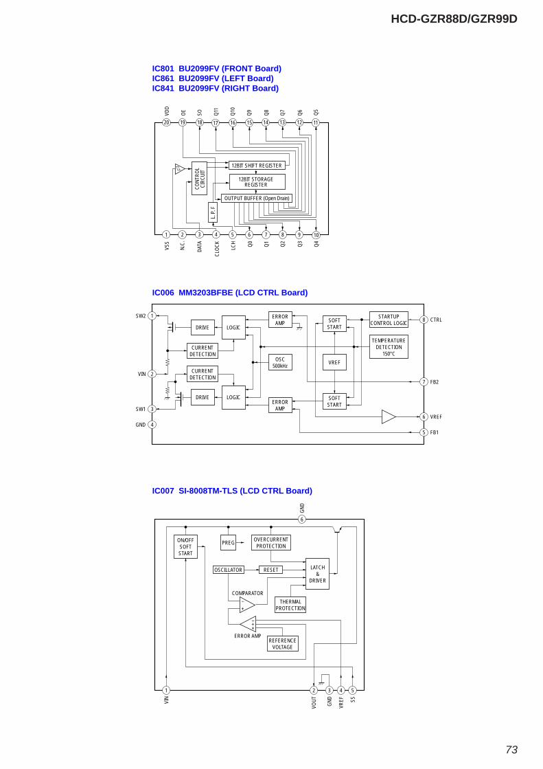
HCD-GZR88D/GZR99D
73
IC801 BU2099FV (FRONT Board)IC861 BU2099FV (LEFT Board)IC841 BU2099FV (RIGHT Board)
IC006 MM3203BFBE (LCD CTRL Board)
IC007 SI-8008TM-TLS (LCD CTRL Board)
12BIT SHIFT REGISTER
12BIT STORAGEREGISTERCO
NTRO
LCI
RCUI
T
L. P.
F
VDD
OE SO Q11
Q10
Q9 Q8 Q7 Q6 Q5
1 2 3 5 6 7 84 10
16 15 14 13 12 11
9
17181920
VSS
N.C.
DATA
CLOC
K
LCH Q0 Q1 Q2 Q3 Q4
OUTPUT BUFFER (Open Drain)
TEMPERATUREDETECTION
150°C
FB15
FB27VIN 2
VREF6
SW2 1
DRIVE
VREF
LOGIC
CURRENTDETECTION
GND 4
SW1 3
DRIVE LOGIC
CURRENTDETECTION
ERRORAMP
ERRORAMP
OSC500kHz
SOFTSTART
SOFTSTART
CTRL8STARTUPCONTROL LOGIC
1 2 54
LATCH&
DRIVER
ERROR AMP
COMPARATOR
OSCILLATOR RESET
OVERCURRENTPROTECTION
THERMALPROTECTION
REFERENCEVOLTAGE
3
ON/OFFSOFTSTART
PREG
+
++
–
–
VIN
VOUT
6
GND
SS
VREF
GND
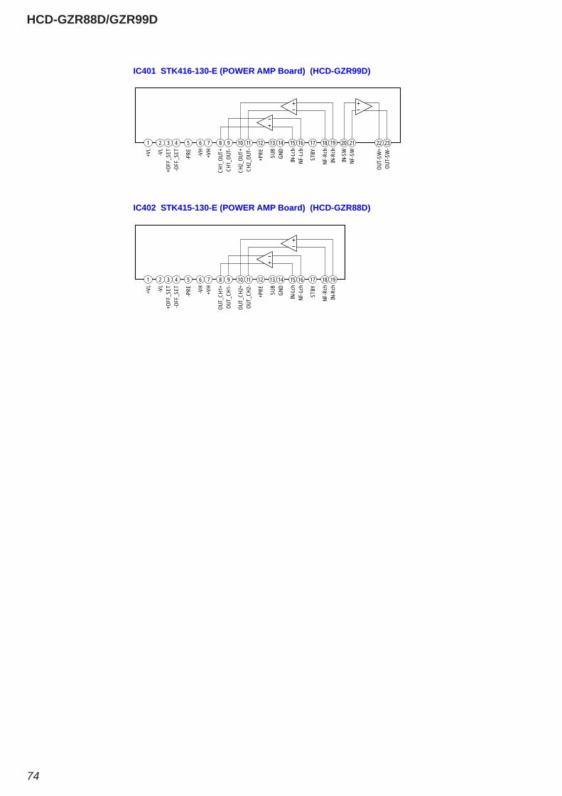
HCD-GZR88D/GZR99D
74
IC401 STK416-130-E (POWER AMP Board) (HCD-GZR99D)
IC402 STK415-130-E (POWER AMP Board) (HCD-GZR88D)
5 6 8 9 10 11 12 13 14 15 16 17
-PRE -VH
OUT_
CH1+
OUT_
CH1-
OUT_
CH2+
OUT_
CH2-
+PRE SU
BGN
D
IN-L
chNF
-Lch
STBY
4
-OFF
_SET
18 19
NF-R
chIN
-Rch
2 3
-VL
+OFF
_SET
1
+VL
7
+VH
5 6 8 9 10 11 12 13 14 15 16 17
-PRE -VH
CH1_
OUT+
CH1_
OUT-
CH2_
OUT+
CH2_
OUT-
+PRE SU
BGN
D
IN-L
chNF
-Lch
STBY
4
-OFF
_SET
18 19
NF-R
chIN
-Rch
20 21
IN-S
WNF
-SW
22 23
OUT-
SW+
OUT-
SW-
2 3
-VL
+OFF
_SET
1+V
L7
+VH

HCD-GZR88D/GZR99D
75
• IC Pin Function DescriptionsDMB19 BOARD (2/4) IC101 CXD9971R (CD/DVD RF AMP, FOCUS/TRACKING ERROR AMP, DVD SYSTEMPROCESSOR, DIGITAL SERVO PROCESSOR)
Pin No. Pin Name I/O Description1 RF_A I RF main beam (C) signal input from the optical pick-up block2 RF_B I RF main beam (B) signal input from the optical pick-up block3 RF_C I RF main beam (A) signal input from the optical pick-up block4 RF_D I RF main beam (D) signal input from the optical pick-up block5 RF_E I RF sub beam (F) signal input from the optical pick-up block6 RF_F I RF sub beam (E) signal input from the optical pick-up block7 AVDD18_2 — Power supply pin (+1.8 V)8 AVDD33_1 — Power supply pin (+3.3 V)9 XTALI I System clock signal input (27 MHz)10 XTALO O System clock signal output (27 MHz)11 AGND33 — Ground12 V20 O Reference voltage (+2 V) output for the optical pick-up block13 V14/VREFO O Reference voltage (+1.4 V) output14 REXT I Current reference signal input
15, 16 MDI1, MDI2 I Laser power monitor signal input from the optical pick-up block17, 18 LDO1, LDO2 O Laser diode drive signal output for the optical pick-up block
19 AVDD33_2 — Power supply pin (+3.3 V)20 DMO O Spindle motor control signal output for the motor driver21 FMO O Sled motor control signal output for the motor driver22 MUTE4 O Mute signal output for the coil/motor driver (for spindle motor)23 MSW O CD/DVD select signal output (L: CD, H: DVD)24 TRO O Tracking coil control signal output for the coil driver25 FOO O Focus coil control signal output for the coil driver26 EEWP O Write enable signal output for the EEPROM
27, 28 USB_DP, USB_DM I/O Two-way audio serial data input/output with the USB controller29 VDD33_USB — Power supply pin (+3.3 V)30 VSS33_USB — Ground31 PAD_VRT I/O USB generating reference current signal input/output32 VDD18_USB — Power supply pin (+1.8 V)33 SCL O Serial clock signal output for the EEPROM34 SDA I/O Two-way serial data input/output with the EEPROM35 IFSDI I Serial data input from the system control36 SF_CS# O Chip select signal output for the SF-ROM37 SF_DO O Serial data output for the SF-ROM38 SF_DI I Serial data input from the SF-ROM39 SF_CK O Serial clock signal output for the SF-ROM40 IFSCK O Serial data transfer clock signal output for the system control41 IFSDO O Serial data output for the system control42 ICE I ICE mode enable setting pin (Not used in this set)43 PRST# I Reset signal input from the system control (L: reset)44 IR I IR control signal input (Not used in this set)
45 to 49 RD0 to RD4 I/O Two-way data bus input/output with the 64M SDRAM50 DVDD33 — Power supply pin (+3.3 V)
51 to 53 RD5 to RD7 I/O Two-way data bus input/output with the 64M SDRAM54 DVDD18 — Power supply pin (+1.8 V)55 DQM0 O Data mask signal output for the 64M SDRAM
56 to 59 RD15 to RD12 I/O Two-way data bus input/output with the 64M SDRAM60 DVSS33 — Ground
61 to 64 RD11 to RD8 I/O Two-way data bus input/output with the 64M SDRAM65 DQM1 O Data mask signal output for the 64M SDRAM66 RCLK O Clock signal output for the 64M SDRAM67 RA11 O Address signal output for the 64M SDRAM68 DVDD33 — Power supply pin (+3.3 V)

HCD-GZR88D/GZR99D
76
Pin No. Pin Name I/O Description69 to 74 RA9 to RA4 O Address signal output for the 64M SDRAM
75 RWE# O Write enable signal output for the 64M SDRAM76 CAS# O Column address strobe signal output for the 64M SDRAM77 RAS# O Row address strobe signal output for the 64M SDRAM78 BA0 O Bank address signal output for the 64M SDRAM79 DVSS18 — Ground80 BA1 O Bank address signal output for the 64M SDRAM
81 to 83 RA10, RA0, RA1 O Address signal output for the 64M SDRAM84 DVDD33 — Power supply pin (+3.3 V)
85, 86 RA2, RA3 O Address signal output for the 64M SDRAM87 IFBSY I Communication initialization request signal input from the system control88 IFCS# O Communication initialization request acknowledge signal output for the system control89 RX — Not used in this set90 DVDD18 — Power supply pin (+1.8 V)91 TX — Not used in this set92 XMAMUTE — Not used in this set93 SPDIF O SPDIF signal output94 TSDM I Thermal shut down signal input from the coil/motor driver95 DACVDDC — Power supply pin (+3.3 V)96 VREF I Band gap reference voltage input97 FS I Full scale adjustment signal input98 DACVSSC — Ground99 CVBS O Composite video signal output100 DACVDDB — Power supply pin (+3.3 V)101 DACVDDA — Power supply pin (+3.3 V)102 SY/Y/G O Component video (Y) signal output103 SC/CB/B O Component video (Pb/Cb) signal output104 CR/R O Component video (Pr/Cr) signal output105 AADVSS — Ground106 ADIN I Audio data input from the A/D converter (for USB)107 MUTE123 O Not used in this set108 LIMITSW I Not used in this set109 AADVDD — Power supply pin (+3.3 V)110 APLLVDD — Power supply pin (+3.3 V)111 APLLCAP I External capacitor connecting pin112 ADACVSS2 — Ground113 ADACVSS1 — Ground114 ACLK O Master clock signal output for the A/D converter and D/A converter115 ABCK O Bit clock signal output for the A/D converter and D/A converter116 MUTE123 O Mute signal output for the coil/motor driver (for focus/tracking coil and sled motor)117 AVCM I Audio D/A converter reference voltage input118 LIMITSW I Limit detection switch signal input119 ALRCK O L/R sampling clock signal output for the A/D converter and D/A converter120 ASDATA0 O Audio data output for the D/A converter121 ADACVDD1 — Power supply pin (+3.3 V)122 ADACVDD2 — Power supply pin (+3.3 V)123 AVDD18_1 — Power supply pin (+1.8 V)124 AGND18 — Ground125 RFIP I AC coupled RF signal input from the optical pick-up block126 OPOUT O AC coupled RF signal output for the optical pick-up block127 IOPMON I Power monitor pin128 SPFG I Spindle motor hall sensor input from the motor driver

HCD-GZR88D/GZR99D
77
MAIN BOARD (1/3) IC501 μPD78F1105GF(S)-GAS-AX (SYSTEM CONTROL)
Pin No. Pin Name I/O Description1 IIC SCL O IIC clock (GC micon) signal output2 IIC SDA O IIC data (GC micon) signal output3 O-FRONT-MUTE O Front speaker output mute (L: mute ON)4 O-SW-MUTE O Subwoofer output mute (L: mute ON)5 O-TC-REC-REV I Tape deck signal input6 O-TC-B-TRIG O Tape deck B trigger plunger control signal output7 O-EEP-SCL O EEPROM communication (Clock) signal output (Not used in this set)8 O-EEP-SDA I/O EEPROM communication (Data) signal input/output (Not used in this set)9 O-iPod/WM-SW O iPod adaptor power supply control signal output (H: power supply) (Not used in this set)10 O-TC-A-TRIG O Tape deck A trigger plunger control signal output11 O-GC/LCD-RESET O LCD reset signal output12 I-TU-RDS-INT I Tuner RDS initial setting signal input (Not used in this set)13 I-AC-CUT I AC cut decision signal input (L: AC cut)14 O-TC-CAPM-CNT O Capstan motor control signal output15 O-AUDIO_IC-DATA O R2A15216FP (IC101) communication (Data) signal output16 O-AUDIO_IC-CLK O R2A15216FP (IC101) communication (Clock) signal output17 O-TC-REC/PB_SW O Tape deck control signal output18 O-TC-REC-MUTE O Tape deck B recording mute signal output19 O-TC-REC-BIAS O Recording bias control signal output20 EVSS1 — Ground21 O-STK-MUTE O Front speaker output mute signal output (L: mute)
22 I-iPod/WM-OVER-CURRENT I iPod over-current detect signal input (Not used in this set)
23 I-USB-OVER-CURRENT I USB over-current detect signal input
24 O-DVD-POWER O DMB19 board power supply control signal output25 O-FRONT-SP-RELAY O Front speaker relay control signal output (L: relay ON)26 O-TU-DI O Tuner IC communication (Data: MCU → TUNER) signal output27 O-TU-CLK O Tuner IC communication (Clock) signal output28 I-TU-DO I Tuner IC communication (Data: MCU ← TUNER) signal input29 O-TU-CE O Tuner IC communication (Chip enable) signal output30 EVDD1 — Power supply pin (+3.3 V)31 I-TU-TUNE I Tuner tuned data input32 I-CDM-OPEN I Disc tray open signal input (L: open)33 I-CDM-TBL-ADR-SW I Disc tray position signal input34 O-CDM-TM-F O Disc table motor control signal output35 O-CDM-TM-R O Disc table motor control signal output36 O-CDM-LM-F O Disc tray motor control signal output37 O-CDM-LM-R O Disc tray motor control signal output38 O-SW-SP-RELAY O Subwoofer relay control signal output (L: relay ON) (Not used in this set)39 O-MTK-A/D-IN-SEL O DMB19 board input audio signal control signal output (L: mic, H: audio)40 I-ACF-DET I AC power supply frequency detect signal input41 O-MTK-MTRST O MTK IC reset signal output (L: reset)42 I-DVD-XIFS I DMB19 board communication signal input43 O-MTK-IFBSY O DMB19 board communication (Interface busy) signal output44 O-MTK-DATA O DMB19 board communication (Data: MCU → DMB19 board) signal output45 I-MTK-DATA I DMB19 board communication (Data: MCU ← DMB19 board) signal input46 I-MTK-CLK I DMB19 board communication (Clock) signal input47 AVREF1 — Analog reference voltage (+3.3 V)48 O-FAN O Fan motor control signal output (Not used in this set)49 O-STBY-RELAY O Main power relay signal output (H: relay ON)50 AVREF0 — Analog reference voltage (+3.3 V)51 AVSS — Analog ground
52 I-POWER-MONITOR(ACP) I Main power monitor signal input

HCD-GZR88D/GZR99D
78
Pin No. Pin Name I/O Description53 I-MODEL I Model identifi cation signal input54 I-DESTINATION I Destination identifi cation signal input
55 DVD-POWER-MONITOR(3.3V) I MTK board power monitor signal input
56 I-CDM-ENC(E1,E2,E3) I Disc tray signal input57 I-MIC/HP-DET I Mic in/headphone signal input58 I-VACS I Tape deck VACS signal input59 I-ILLUMINATION I Audio level signal input for illumination
60 I-TC-STAT(A-HALF/B-HALF/REC-FWD) I Tape deck signal input
61 I-VOL I Volume signal input62 I-KEY4 I Key 4 signal input63 I-KEY3 I Key 3 signal input64 I-KEY2 I Key 2 signal input65 I-KEY1 I Key 1 signal input
66 I-iPod-OPERATION-MODE I iPod micon communication (Operation mode) signal input (Not used in this set)
67 O-iPod-NTSC/PAL O iPod micon communication (Color system) signal output (Not used in this set)68 O-LED-STBY O STANDBY LED control signal output (H: light ON)69 O-S/P-RESET O LED control IC reset signal output70 O-S/P-CLK O LED control IC communication (Clock) signal output71 O-S/P-OE O LED control IC communication (Output enable) signal output72 O-S/P-DATA O LED control IC communication (Data: MCU → Control IC) signal output73 O-USB-POWER O USB power supply control signal output74 TC-A-SHUT I Deck A shut off signal input75 TC-B-SHUT I Deck B shut off signal input76 O-iPod-DATA(TxD) O iPod micon communication (Data: MCU → iPod micon) signal output (Not used in this set)77 I-iPod-DATA(RxD) I iPod micon communication (Data: MCU ← iPod micon) signal input (Not used in this set)78 O-iPod-RESET O iPod micon reset signal output (Not used in this set)79 USB-LED-BLUE O USB illuminator LED (Blue) control signal output80 USB-LED-RED O USB illuminator LED (Red) control signal output81 I-SIRCS I Remote control signal receiver sircs signal input82 I-DISPLAY-KEY I Display key interrupt signal input83 I-POWER-KEY I Power key interrupt signal input84 I-TU-RDS-DATA I Tuner RDS data signal input (Not used in this set)
85, 86 O-VIDEO-SW-A,O-VIDEO-SW-B O Video output selector (SW-A, SW-B) signal output (L, L: iPod), (L, H: mute), (H, L: VIDEO/SAT),
(H, H: DMB19 board)
87 O-VIDEO-MUTE O Video mute signal output88 O-VIDEO-I/P O COMPONENT VIDEO OUT select signal output (L: progressive, H: interlace)89 SI/SO I/O Data input/output for fl ash programmer90 RESET I System reset signal input91 XT2 I Sub system clock signal input (32.768 kHz)92 XT1 O Sub system clock signal output (32.768 kHz)93 FLMD0 I FL mode setting signal input94 X2 I Main system clock signal input (20 MHz)95 X1 O Main system clock signal output (20 MHz)96 REGC — Regulator ripple capacitor connecting97 VSS — Ground98 EVSS — Ground99 VDD — Power supply pin (+3.3 V)100 EVDD0 — Power supply pin (+3.3 V)

HCD-GZR88D/GZR99D
79
LCD CTRL BOARD IC002 TW8827-TA3-GR (LCD CONTROL)
Pin No. Pin Name I/O Description1 AVD1 — Power supply pin (+1.8 V)2 YIN1 I Analog composite signal input 1 (Connect to AVS)3 YIN0 I Analog composite signal input 04 YGND — Ground5 YOUT O Y signal output (Not used in this set)6 AVS1 — Ground7 CIN I Analog component C signal input (Connect to AVS)8 AVD2 — Power supply pin (+1.8 V)9 AVS2 — Ground
10 FPBIAS O Flat panel back light bias power on/off control signal output11 FPPWM1 O Flat panel power monitor signal output (Not used in this set)12 VDD18_1 — Power supply pin (+1.8 V)13 VSS18_1 — Ground14 TCLRL O TCON left/right select signal output (L: right, H: left)15 FPPWC O Flat panel power on/off control signal output16 TRCLK O TCON row driver shift clock signal output17 TRUDL/GPO1 O TCON up/down select signal output (L: down, H: up)/general purpose signal output
18 TCINV/GPO2 O TCON column driver inversion signal output/general purpose signal output (Not used in this set)
19 POL_A/GPO3 O TCON column driver polarity A signal output/general purpose signal output (Not used in this set)
20 POL_B/GPO4 O TCON column driver polarity B signal output/general purpose signal output21 TCLP O TCON column driver load pulse signal output22 FPCLK O Flat panel clock signal output23 VDD33_1 — Power supply pin (+3.3 V)24 VSS33_1 — Ground25 TRSPT/FPVS O TCON row driver starting pulse (top start) signal output/fl at panel vertical sync signal output
26 TCSPL/FPHS O TCON column driver starting pulse (left to right scan) signal output/fl at panel horizontalsync signal output
27 TROE/FPDE O TCON row driver output enable signal output/fl at panel data valid signal output
28 TCSPR/GPO5 O TCON column driver starting pulse (right to left scan) signal output/general purpose signal output
29 TRSPB/GPO6 O TCON row driver starting pulse (bottom start) signal output/general purpose signal output30 to 33 DTV0 to DTV3 I DTV signal input 0 to 3 (Not used in this set)
34 VDD18_2 — Power supply pin (+1.8 V)35 VSS18_2 — Ground
36 to 39 DTV4 to DTV7 I/O DTV signal input 4 to 7 (Not used in this set)40 VDD33_2 — Power supply pin (+3.3 V)41 VSS33_2 — Ground
42 to 49 DTV8/P2.0 to DTV15/P2.7 I/O DTV signal input 8 to 15/MCU port signal input 2.0 to 2.7 (Not used in this set)
50 DTVCLK I/O DTV interface clock signal input (Not used in this set)51 DTVVS I/O DTV interface vertical sync signal input (Not used in this set)52 DTVHS I/O DTV interface horizontal sync signal input (Not used in this set)53 DTVDE/P3.2/INT I/O DTV interface data valid signal input/MCU port signal input 3.2 (MCU int0)54 XOUT O System clock signal output (27 MHz)55 XIN I System clock signal input (27 MHz)56 RESET I Reset signal input57 TEST1 I Production test pin (Connect to VSS33)58 VDD33_3 — Power supply pin (+3.3 V)59 VSS33_3 — Ground60 PWR_DN I Power down signal input (Connect to VSS33)61 MCU_EN I MCU enable signal input (Fixed at L in this set)62 SDAT/P1.1 I/O 2-wire IIC interface data input/output//MCU port signal input/output 1.1

HCD-GZR88D/GZR99D
80
Pin No. Pin Name I/O Description63 SCLK/P1.0 I/O 2-wire IIC interface clock signal input/output//MCU port signal input/output 1.164 RXD/P3.0 I/O MCU RXD signal input/MCU port signal input 3.0 (Not used in this set)65 TXD/P3.1 I/O MCU TXD signal output/MCU port signal output 3.1 (Not used in this set)66 VDD18_3 — Power supply pin (+1.8 V)67 VSS18_3 — Ground68 SPI_CSN O SPI CS (low enable) signal output (Not used in this set)69 SPI_SDO O SPI data out signal output (Not used in this set)70 SPI_SDI I SPI data in signal input (Connect to VSS18)71 SPI_CLK O SPI clock out signal output (Not used in this set)72 AVD3 — Power supply pin (+3.3 V)73 ROUT O DAC analog red data output74 GOUT O DAC analog green data output75 BOUT O DAC analog blue data output
76, 77 SENSE0, SENSE1 I Analog sensing 0, 1 signal input78, 79 ADCIN1, ADCIN0 I Low speed ADC input 1, 0
80 AVS3 — Ground

81
HCD-GZR88D/GZR99DSECTION 7
EXPLODED VIEWS
1 4-124-002-22 PANEL, LOADING (GZR88D) 1 4-124-002-32 PANEL, LOADING (GZR99D) 2 4-124-014-01 CASE (SIDE R) 3 3-363-099-02 SCREW (CASE 3 TP2) 4 4-124-013-01 CASE (SIDE L) (GZR99D)
4 4-124-013-11 CASE (SIDE L) (GZR88D) 5 3-285-881-01 COVER (FAN) 6 1-828-935-11 WIRE (FLAT TYPE) (5 CORE) 7 4-124-009-21 PANEL (TOP) (GZR99D:E2,E51,AR,MX)
8 3-087-053-01 +BVTP2.6 (3CR) (GZR99D:E2,E51,AR,MX) FAN901 1-787-400-31 FAN (DC) (GZR88D) FAN901 1-787-631-11 FAN (DC) (GZR99D) #1 7-685-646-79 SCREW +BVTP 3X8 TYPE2 IT-3 #2 7-685-647-79 SCREW +BVTP 3X10 TYPE2 IT-3
#3 7-685-645-79 SCREW +BVTP 3X6 TYPE2 IT-3 #4 7-685-903-21 TAPPING +PWH 3X8 TYPE2 N-S #5 7-685-144-11 SCREW +P 3X5 TYPE2 N-S
Ref. No. Part No. Description Remark Ref. No. Part No. Description Remark
The components identifi ed by mark 0 or dotted line with mark 0 are critical for safety.Replace only with part number specifi ed.
7-1. OVERALL SECTION
Note:• -XX and -X mean standardized parts, so
they may have some difference from the original one.
• Items marked “*” are not stocked since they are seldom required for routine ser-vice. Some delay should be anticipated when ordering these items.
• The mechanical parts with no reference number in the exploded views are not sup-plied.
• Accessories are given in the last of the electrical parts list.
• Abbreviation E2 : 120V AC area in E model E51 : Chilean and Peruvian model AR : Argentina model MX : Mexican model E3 : 240V AC area in E model E4 : 110 – 120V/220 – 240V AC area in E model E15 : Iran model PH : Philippines model SP : Singapore model E12 : 220 – 240V AC area in E model TH : Thai model
#4
#1
#1
#1
#2
#1
#3
#3
#1
#3 #3#3
#3
#3#3
#5
#5#4
#1#1
#1
chassis section
front panel section-1
top panel section
HCD-GZR99D: E2, E51, AR, MX MODEL EXCEPT HCD-GZR99D: E2, E51, AR, MX MODEL
1
3
34
5
6
7
8
8
2
not supplied(VIDEO board)
not supplied(TRANS-SUB board)
not supplied
not supplied
not supplied
FAN901
A
A
#1
A

82
HCD-GZR88D/GZR99D
Ref. No. Part No. Description Remark Ref. No. Part No. Description Remark
51 X-2349-503-1 PANEL (MAIN) ASSY (GZR99D:E3,E4,E15,PH,SP) 51 X-2349-504-1 PANEL (MAIN) ASSY (GZR99D:E2,E51,AR,MX) 51 X-2349-505-1 PANEL (MAIN) ASSY (GZR88D) 52 4-225-252-01 CUSHION (FOOT) 53 2-638-220-21 KNOB (MIC)
54 3-087-053-01 +BVTP2.6 (3CR) 55 1-837-124-11 WIRE (FLAT TYPE) (5 CORE) 56 4-123-994-01 BUTTON (ENTER) 57 4-123-993-01 BUTTON (CURSOR)
7-2. FRONT PANEL SECTION-1
51
52
53
54
54
54
54
5457
56
54
54
54
55
front panel section-2
not supplied(HP board)
not supplied(LEFT board)
not supplied(RIGHT board)
not supplied(HP-JACK HOLDER board)
not supplied(MIC board)
not supplied(USB-LED board)
not supplied
55

83
HCD-GZR88D/GZR99D
Ref. No. Part No. Description Remark Ref. No. Part No. Description Remark
101 X-2349-510-1 PANEL (LCD) ASSY (EXCEPT GZR99D:E2,E51,AR,MX) 101 X-2349-511-1 PANEL (LCD) ASSY (GZR99D:E2,E51,AR,MX) 102 3-087-053-01 +BVTP2.6 (3CR) 103 4-123-988-01 PLATE (JOG) 104 4-123-989-11 KNOB (JOG)
105 4-145-107-01 SPRING KNOB 106 4-128-320-01 HOLDER (KNOB) 107 X-2349-514-1 KNOB (VOL) ASSY 108 4-124-004-01 RUBBER (VOL) 109 4-124-001-01 CUSHION (LCD)
110 A-1671-636-A LCD CTRL BOARD, COMPLETE 111 4-123-982-01 BUTTON (DISP) 112 4-123-983-01 BUTTON (REC)
(EXCEPT GZR99D:E2,E51,AR,MX) 112 4-123-983-11 BUTTON (REC) (GZR99D:E2,E51,AR,MX) 113 X-2349-513-1 BUTTON (DISC) ASSY
114 1-831-964-21 WIRE (FLAT TYPE) (21 CORE) 115 4-124-001-11 CUSHION (LCD) 116 1-828-946-51 WIRE (FLAT TYPE) (7 CORE) 117 1-457-413-11 CORE, FERRITE LCD101 1-802-937-11 DISPLAY PANEL, LIQUID CRYSTAL
7-3. FRONT PANEL SECTION-2
supplied with S891
102
102102
102
102
102
102
101
102
103
104
105106
107
108
110
116 117
115
115
109
109
111
114
112
113
not supplied(FRONT board)
not supplied(VOLUME board)
not supplied
not supplied
LCD101

84
HCD-GZR88D/GZR99D
Ref. No. Part No. Description Remark Ref. No. Part No. Description Remark
151 4-124-010-01 LID (TC-L) 152 4-124-021-01 SPRING (TC-L) 153 2-669-613-01 DETENT SPRING 154 4-124-022-01 SPRING (TC-R) 155 4-124-011-01 LID (TC-R)
156 4-224-104-41 DAMPER 157 4-124-008-01 PANEL (TOP TC) 158 4-231-824-01 CAM (A), HEART 159 4-231-836-01 SPRING (HEART CAM-A)
160 4-231-825-01 CAM (B), HEART 161 4-231-841-01 SPRING (HEART CAM-B) 162 3-087-053-01 +BVTP2.6 (3CR) 163 1-840-233-11 DECK, MECHANICAL (CWP42FR605) 164 3-274-426-01 BELT (FR)
165 4-148-152-01 BELT (AF) 166 4-148-154-01 BELT (BR) 167 1-833-868-11 WIRE (FLAT TYPE) (11 CORE)
7-4. TOP PANEL SECTION (EXCEPT HCD-GZR99D: E2, E51, AR, MX MODEL)
151152
153
154
155
156
156
157
158159
160
161
162
162
162
162
163164 164
165166
167
162
not supplied(TC-AMP board)
not supplied

85
HCD-GZR88D/GZR99D
Ref. No. Part No. Description Remark Ref. No. Part No. Description Remark 201 A-1675-105-A MAIN BOARD, COMPLETE (GZR88D:E3,E15) 201 A-1675-106-A MAIN BOARD, COMPLETE (GZR88D:E4,E12) 201 A-1675-107-A MAIN BOARD, COMPLETE (GZR88D:PH,SP,TH) 201 A-1675-108-A MAIN BOARD, COMPLETE (GZR99D:E3,E15) 201 A-1675-109-A MAIN BOARD, COMPLETE (GZR99D:E4)
201 A-1675-110-A MAIN BOARD, COMPLETE (GZR99D:PH,SP) 201 A-1675-111-A MAIN BOARD, COMPLETE (GZR99D:E2) 201 A-1675-112-A MAIN BOARD, COMPLETE (GZR99D:E51,AR) 201 A-1730-608-A MAIN BOARD, COMPLETE (GZR99D:MX) 202 3-655-653-11 BAND (TAITON), BINDING
203 1-543-929-11 CORE, FERRITE 204 1-828-965-51 WIRE (FLAT TYPE) (11 CORE) (EXCEPT GZR99D:E2,E51,AR,MX) 205 1-828-956-51 WIRE (FLAT TYPE) (9 CORE) 206 A-1719-741-A DMB19 BOARD, COMPLETE (for SERVICE) (GZR99D:E3,E15) 206 A-1719-743-A DMB19 BOARD, COMPLETE (for SERVICE) (GZR99D:E4)
206 A-1719-744-A DMB19 BOARD, COMPLETE (for SERVICE) (GZR99D:PH,SP) 206 A-1719-745-A DMB19 BOARD, COMPLETE (for SERVICE) (GZR99D:E2,E51,AR) 206 A-1719-746-A DMB19 BOARD, COMPLETE (for SERVICE) (GZR88D:E3,E15)
206 A-1719-747-A DMB19 BOARD, COMPLETE (for SERVICE) (GZR88D:E4,E12) 206 A-1719-748-A DMB19 BOARD, COMPLETE (for SERVICE) (GZR88D:PH,SP,TH) 206 A-1736-114-A DMB19 BOARD, COMPLETE (for SERVICE) (GZR99D:MX) 207 1-830-459-51 WIRE (FLAT TYPE) (7 CORE) 208 1-837-127-11 WIRE (FLAT TYPE) (7 CORE)
209 1-837-125-11 WIRE (FLAT TYPE) (9 CORE) 210 4-225-252-01 CUSHION (FOOT) 211 3-087-053-01 +BVTP2.6 (3CR) 212 1-828-973-11 WIRE (FLAT TYPE) (13 CORE) 213 3-905-609-31 SCREW (TRANSISTOR)
214 4-900-386-01 SCREW0 215 1-569-008-33 ADAPTOR, CONVERSION 2P (E2,E3,E4,E15,E51,PH,SP)0 216 1-829-387-11 CORD, POWER (AR)0 216 1-834-288-11 CORD, POWER (TH)0 216 1-834-966-41 POWER-SUPPLY CORD (EXCEPT TH,AR,MX)
0 216 1-835-080-21 CORD, POWER (MX) 217 3-703-244-00 BUSHING (2104), CORD (EXCEPT TH,MX)* 217 3-703-571-12 BUSHING (S) (4516), CORD (MX) 217 4-916-783-01 BUSHING, CORD (TH)
7-5. CHASSIS SECTION-1
201204
205
210
203
202
220
212
213218
217216
215
211
211208
207 219
206
209
214
not supplied(WIRE HOLDER C board)
not supplied(WIRE HOLDER A board)
not supplied(WIRE HOLDER B board)
not supplied
not supplied
not supplied
not supplied
not supplied
not supplied
#1
#1
#1
#1
#1
#1#3
#1
#1
#1
#1 #1
#1
#1#1
#1
#1
#3
#1
#1
TM901
F301PT301
F302
F304
F305F306
F303
not supplied(TRANS board)
not supplied(POWER AMP board)
CDM74HF-DVBU101
– Continued on next page –

86
HCD-GZR88D/GZR99D
Ref. No. Part No. Description Remark Ref. No. Part No. Description Remark 218 1-457-369-12 CORE, FERRITE 219 2-580-644-11 SCREW, +KTP2 3X8 220 4-152-150-01 CAP (DMB)0 F301 1-532-465-33 FUSE (T3.15AL/250V)0 F302 1-532-505-33 FUSE (T5AL/250V)
0 F303 1-576-332-33 FUSE, CYLINDRICAL (TIME LAG) (T10AL/250V)0 F304 1-533-949-33 FUSE, CYLINDRICAL (TIME LAG) (T8AL/250V) (GZR88D)0 F304 1-576-332-33 FUSE, CYLINDRICAL (TIME LAG) (T10AL/250V) (GZR99D)
0 F305 1-533-949-33 FUSE, CYLINDRICAL (TIME LAG) (T8AL/250V) (GZR88D)0 F305 1-576-332-33 FUSE, CYLINDRICAL (TIME LAG) (T10AL/250V) (GZR99D)0 F306 1-576-332-33 FUSE, CYLINDRICAL (TIME LAG) (T10AL/250V)0 PT301 1-445-681-11 TRANSFORMER, POWER (MAIN) (GZR99D)0 PT301 1-445-684-11 TRANSFORMER, POWER (MAIN) (GZR88D)
TM901 1-693-778-11 TUNER (FM/AM) (ANTENNA) #1 7-685-646-79 SCREW +BVTP 3X8 TYPE2 IT-3 #3 7-685-645-79 SCREW +BVTP 3X6 TYPE2 IT-3
7-6. CHASSIS SECTION-2
201204
205
210
203
202
220
212
213218
217216
215
211
211208
207 219
206
209
214
not supplied(WIRE HOLDER C board)
not supplied(WIRE HOLDER A board)
not supplied(WIRE HOLDER B board)
not supplied
not supplied
not supplied
not supplied
not supplied
not supplied
#1
#1
#1
#1
#1
#1#3
#1
#1
#1
#1 #1
#1
#1#1
#1
#1
#3
#1
#1
TM901
F301PT301
F302
F304
F305F306
F303
not supplied(TRANS board)
not supplied(POWER AMP board)
CDM74HF-DVBU101

87
HCD-GZR88D/GZR99D
Ref. No. Part No. Description Remark Ref. No. Part No. Description Remark
251 4-218-253-62 SCREW (M2.6), +BTTP 252 1-776-182-11 WIRE (FLAT TYPE) (5 CORE) 253 1-687-134-12 MOTOR (TB) BOARD 254 4-243-815-11 TABLE (LOADING) 255 4-245-571-02 GEAR (STOPPER)
256 4-218-252-61 SCREW (+PTPWH M2.6), FLOATING 257 4-245-570-01 GEAR (JOINT) 258 4-245-572-01 BUSHING (GEAR) 259 1-687-132-12 SENSOR BOARD
260 4-243-820-01 GEAR (TABLE) 261 4-243-819-01 GEAR (GENEVA) 262 4-243-816-21 TRAY 263 4-243-823-11 BELT (TABLE) 264 4-985-672-01 SCREW (+PTPWH M2.6), FLOATING
265 4-243-821-01 PULLEY (TABLE) 266 3-231-598-01 SHEET (BA) M741 A-1108-965-A MOTOR ASSY, TABLE (TABLE)
7-7. DVD MECHANISM DECK SECTION-1 (CDM74HF-DVBU101)
251
252
266
253254
255255
256
256257
257
258
258259
251
256
262
263
264265260
261264
M741
chassis assy

88
HCD-GZR88D/GZR99D
Ref. No. Part No. Description Remark Ref. No. Part No. Description Remark
7-8. DVD MECHANISM DECK SECTION-2 (CDM74HF-DVBU101)
301
302
303
302
302
304
305
305306
307
308
309
310
311 312
313
314
315316
317324
318
318
319325
319
319319
320
321
323
322
305
305
305
M751
not supplied
not supplied
not supplied
RE701
301 A-1103-756-B DRIVER BOARD, COMPLETE 302 4-218-253-52 SCREW (M2.6), +BTTP 303 1-687-669-12 SW BOARD 304 4-244-034-11 BELT (LOADING) 305 4-985-672-01 SCREW (+PTPWH M2.6), FLOATING
306 4-225-844-01 GEAR (LOADING A) 307 4-224-613-11 GEAR (SHAFT) 308 1-687-133-12 MOTOR (LD) BOARD 309 4-244-108-01 GEAR, SWING 310 4-224-609-01 GEAR (LOADING C)
311 4-224-608-01 COLLAR, SWING 312 3-016-533-11 WASHER (FR), STOPPER 313 4-224-611-01 GEAR (LOADING B) 314 4-224-606-01 GEAR (RV)
315 4-243-818-01 GEAR (U/D) 316 2-541-918-01 LEVER (LIFTER (H)) 317 2-345-983-01 PULLEY B (310), CHUCKING 318 3-087-599-01 SCREW, INSULATOR 319 2-634-618-01 INSULATOR
320 1-828-251-51 WIRE (FLAT TYPE) (24 CORE)0 321 8-820-322-04 OPTICAL PICK-UP (KHM-313CAB/C2RP) 322 4-251-923-01 YOKE (310) 323 2-345-982-01 PULLEY A (310), CHUCKING 324 4-243-817-22 CHASSIS
325 3-113-851-01 SHEET M751 A-1108-966-A MOTOR ASSY, LOADING (LOADING) RE701 1-477-680-12 ENCODER, ROTARY (DISC TRAY ADDRESS DETECT)

89
HCD-GZR88D/GZR99DSECTION 8
ELECTRICAL PARTS LIST
A-1719-741-A DMB19 BOARD, COMPLETE (for SERVICE) (GZR99D:E3,E15) A-1719-743-A DMB19 BOARD, COMPLETE (for SERVICE) (GZR99D:E4) A-1719-744-A DMB19 BOARD, COMPLETE (for SERVICE) (GZR99D:PH,SP) A-1719-745-A DMB19 BOARD, COMPLETE (for SERVICE) (GZR99D:E2,E51,AR) A-1719-746-A DMB19 BOARD, COMPLETE (for SERVICE) (GZR88D:E3,E15)
A-1719-747-A DMB19 BOARD, COMPLETE (for SERVICE) (GZR88D:E4,E12) A-1719-748-A DMB19 BOARD, COMPLETE (for SERVICE) (GZR88D:PH,SP,TH) A-1736-114-A DMB19 BOARD, COMPLETE (for SERVICE) (GZR99D:MX) **********************
< CAPACITOR >
C101 1-162-970-11 CERAMIC CHIP 0.01uF 10% 25V C102 1-107-826-11 CERAMIC CHIP 0.1uF 10% 16V C105 1-128-994-21 ELECT CHIP 47uF 20% 10V C106 1-162-970-11 CERAMIC CHIP 0.01uF 10% 25V C108 1-162-965-11 CERAMIC CHIP 0.0015uF 10% 50V
C111 1-107-826-11 CERAMIC CHIP 0.1uF 10% 16V C112 1-128-994-21 ELECT CHIP 47uF 20% 10V C113 1-162-970-11 CERAMIC CHIP 0.01uF 10% 25V C115 1-107-826-11 CERAMIC CHIP 0.1uF 10% 16V C116 1-107-826-11 CERAMIC CHIP 0.1uF 10% 16V
C118 1-124-779-00 ELECT CHIP 10uF 20% 16V C119 1-137-710-11 CERAMIC CHIP 10uF 20% 6.3V C124 1-165-908-11 CERAMIC CHIP 1uF 10% 10V C125 1-107-826-11 CERAMIC CHIP 0.1uF 10% 16V C126 1-137-710-11 CERAMIC CHIP 10uF 20% 6.3V
C127 1-165-908-11 CERAMIC CHIP 1uF 10% 10V C144 1-162-970-11 CERAMIC CHIP 0.01uF 10% 25V C145 1-162-970-11 CERAMIC CHIP 0.01uF 10% 25V C146 1-165-908-11 CERAMIC CHIP 1uF 10% 10V C149 1-162-970-11 CERAMIC CHIP 0.01uF 10% 25V
C150 1-162-970-11 CERAMIC CHIP 0.01uF 10% 25V C151 1-162-970-11 CERAMIC CHIP 0.01uF 10% 25V C152 1-162-916-11 CERAMIC CHIP 12PF 5% 50V C153 1-162-916-11 CERAMIC CHIP 12PF 5% 50V C154 1-107-826-11 CERAMIC CHIP 0.1uF 10% 16V
C155 1-107-826-11 CERAMIC CHIP 0.1uF 10% 16V C156 1-162-970-11 CERAMIC CHIP 0.01uF 10% 25V C160 1-162-970-11 CERAMIC CHIP 0.01uF 10% 25V
C168 1-107-826-11 CERAMIC CHIP 0.1uF 10% 16V C169 1-107-826-11 CERAMIC CHIP 0.1uF 10% 16V C172 1-162-970-11 CERAMIC CHIP 0.01uF 10% 25V C175 1-162-970-11 CERAMIC CHIP 0.01uF 10% 25V C179 1-107-826-11 CERAMIC CHIP 0.1uF 10% 16V
C180 1-107-826-11 CERAMIC CHIP 0.1uF 10% 16V C181 1-107-826-11 CERAMIC CHIP 0.1uF 10% 16V C182 1-127-715-11 CERAMIC CHIP 0.22uF 10% 16V C183 1-165-908-11 CERAMIC CHIP 1uF 10% 10V C184 1-162-970-11 CERAMIC CHIP 0.01uF 10% 25V
C186 1-127-715-11 CERAMIC CHIP 0.22uF 10% 16V C188 1-164-315-11 CERAMIC CHIP 470PF 5% 50V C190 1-128-995-21 ELECT CHIP 100uF 20% 10V C191 1-107-826-11 CERAMIC CHIP 0.1uF 10% 16V C192 1-162-970-11 CERAMIC CHIP 0.01uF 10% 25V
C193 1-127-715-11 CERAMIC CHIP 0.22uF 10% 16V C195 1-127-715-11 CERAMIC CHIP 0.22uF 10% 16V C197 1-107-826-11 CERAMIC CHIP 0.1uF 10% 16V C198 1-165-908-11 CERAMIC CHIP 1uF 10% 10V C199 1-162-968-11 CERAMIC CHIP 0.0047uF 10% 50V
C203 1-162-970-11 CERAMIC CHIP 0.01uF 10% 25V C205 1-164-230-11 CERAMIC CHIP 220PF 5% 50V C206 1-164-230-11 CERAMIC CHIP 220PF 5% 50V C208 1-162-970-11 CERAMIC CHIP 0.01uF 10% 25V C209 1-164-677-11 CERAMIC CHIP 0.033uF 10% 16V
C210 1-162-970-11 CERAMIC CHIP 0.01uF 10% 25V C211 1-164-677-11 CERAMIC CHIP 0.033uF 10% 16V C212 1-162-970-11 CERAMIC CHIP 0.01uF 10% 25V C213 1-162-970-11 CERAMIC CHIP 0.01uF 10% 25V C214 1-162-964-11 CERAMIC CHIP 0.001uF 10% 50V
C215 1-162-970-11 CERAMIC CHIP 0.01uF 10% 25V C216 1-162-970-11 CERAMIC CHIP 0.01uF 10% 25V C217 1-117-681-11 ELECT CHIP 100uF 20% 16V C218 1-128-994-21 ELECT CHIP 47uF 20% 10V C219 1-162-970-11 CERAMIC CHIP 0.01uF 10% 25V
C220 1-128-994-21 ELECT CHIP 47uF 20% 10V C221 1-164-360-11 CERAMIC CHIP 0.1uF 16V C222 1-164-360-11 CERAMIC CHIP 0.1uF 16V C224 1-162-970-11 CERAMIC CHIP 0.01uF 10% 25V C233 1-162-968-11 CERAMIC CHIP 0.0047uF 10% 50V
C502 1-125-891-11 CERAMIC CHIP 0.47uF 10% 10V C602 1-128-995-21 ELECT CHIP 100uF 20% 10V C603 1-128-995-21 ELECT CHIP 100uF 20% 10V C604 1-128-995-21 ELECT CHIP 100uF 20% 10V C607 1-115-416-11 CERAMIC CHIP 0.001uF 5% 25V
Ref. No. Part No. Description Remark Ref. No. Part No. Description Remark
When indicating parts by reference num-ber, please include the board name.
Note:• Due to standardization, replacements in
the parts list may be different from the parts specifi ed in the diagrams or the com-ponents used on the set.
• -XX and -X mean standardized parts, so they may have some difference from the original one.
• RESISTORS All resistors are in ohms. METAL: Metal-fi lm resistor. METAL OXIDE: Metal oxide-fi lm resistor. F: nonfl ammable• Items marked “*” are not stocked since
they are seldom required for routine ser-vice. Some delay should be anticipated when ordering these items.
• SEMICONDUCTORS In each case, u: μ, for example: uA. . : μA. . , uPA. . , μPA. . , uPB. . : μPB. . , uPC. . , μPC. . , uPD. . : μPD. .• CAPACITORS uF: μF• COILS uH: μH
The components identifi ed by mark 0 or dotted line with mark 0 are critical for safety.Replace only with part number specifi ed.
DMB19
• Abbreviation E3 : 240V AC area in E model E15 : Iran model E4 : 110 – 120V/220 – 240V AC area in E model PH : Philippines model SP : Singapore model E2 : 120V AC area in E model E51 : Chilean and Peruvian model AR : Argentina model E12 : 220 – 240V AC area in E model TH : Thai model MX : Mexican model

Ref. No. Part No. Description Remark Ref. No. Part No. Description Remark
HCD-GZR88D/GZR99D
90
C610 1-107-826-11 CERAMIC CHIP 0.1uF 10% 16V C611 1-115-416-11 CERAMIC CHIP 0.001uF 5% 25V C620 1-164-360-11 CERAMIC CHIP 0.1uF 16V C621 1-164-360-11 CERAMIC CHIP 0.1uF 16V C622 1-164-360-11 CERAMIC CHIP 0.1uF 16V
C623 1-164-360-11 CERAMIC CHIP 0.1uF 16V C630 1-107-826-11 CERAMIC CHIP 0.1uF 10% 16V C1130 1-162-970-11 CERAMIC CHIP 0.01uF 10% 25V C1504 1-162-960-11 CERAMIC CHIP 220PF 10% 50V C1505 1-162-970-11 CERAMIC CHIP 0.01uF 10% 25V
C1506 1-162-964-11 CERAMIC CHIP 0.001uF 10% 50V C1507 1-107-826-11 CERAMIC CHIP 0.1uF 10% 16V C1510 1-164-360-11 CERAMIC CHIP 0.1uF 16V C1512 1-107-826-11 CERAMIC CHIP 0.1uF 10% 16V C1513 1-107-826-11 CERAMIC CHIP 0.1uF 10% 16V
C4602 1-164-360-11 CERAMIC CHIP 0.1uF 16V C4603 1-164-360-11 CERAMIC CHIP 0.1uF 16V C4606 1-164-360-11 CERAMIC CHIP 0.1uF 16V C4608 1-124-779-00 ELECT CHIP 10uF 20% 16V C4622 1-162-968-11 CERAMIC CHIP 0.0047uF 10% 50V
C4623 1-162-968-11 CERAMIC CHIP 0.0047uF 10% 50V C4626 1-162-970-11 CERAMIC CHIP 0.01uF 10% 25V
< CONNECTOR >
CN101 1-815-763-32 CONNECTOR, FFC/FPC 24P CN105 1-770-470-21 PIN, CONNECTOR (PC BOARD) 6P CN201 1-770-161-21 PIN, CONNECTOR (PC BOARD) 6P CN601 1-778-795-21 PIN, CONNECTOR (PC BOARD) 9P CN1103 1-794-509-11 PIN, CONNECTOR (PC BOARD) 3P
CN1104 1-784-859-51 CONNECTOR, FFC (LIF(NON-ZIF)) 7P* CN1105 1-750-005-11 PIN, CONNECTOR (PC BOARD) 4P CN1106 1-784-861-51 CONNECTOR, FFC (LIF(NON-ZIF)) 9P CN4602 1-784-859-51 CONNECTOR, FFC (LIF(NON-ZIF)) 7P
< DIODE >
D001 6-500-848-01 DIODE MC2840-T112-1 D002 6-500-848-01 DIODE MC2840-T112-1 D003 6-500-848-01 DIODE MC2840-T112-1 D004 6-500-848-01 DIODE MC2840-T112-1 D006 6-500-848-01 DIODE MC2840-T112-1
< EARTH TERMINAL >
ET001 1-780-482-11 TERMINAL, EARTH ET002 1-780-482-11 TERMINAL, EARTH ET003 1-780-482-11 TERMINAL, EARTH ET004 1-780-482-11 TERMINAL, EARTH
< FERRITE BEAD >
FB106 1-469-324-21 FERRITE, EMI (SMD) (2012) FB108 1-469-324-21 FERRITE, EMI (SMD) (2012) FB109 1-469-324-21 FERRITE, EMI (SMD) (2012) FB112 1-469-670-21 FERRITE, EMI (SMD) (2012) FB603 1-469-324-21 FERRITE, EMI (SMD) (2012)
FB606 1-469-324-21 FERRITE, EMI (SMD) (2012) FB607 1-469-324-21 FERRITE, EMI (SMD) (2012) FB608 1-469-324-21 FERRITE, EMI (SMD) (2012) FB609 1-469-324-21 FERRITE, EMI (SMD) (2012) FB1264 1-469-118-21 FERRITE, EMI (SMD) (1608)
FB1265 1-469-118-21 FERRITE, EMI (SMD) (1608) FB1266 1-469-118-21 FERRITE, EMI (SMD) (1608) FB1267 1-469-118-21 FERRITE, EMI (SMD) (1608)
FB1268 1-469-118-21 FERRITE, EMI (SMD) (1608) FB1284 1-414-445-11 FERRITE, EMI (SMD) (1608) FB1285 1-414-445-11 FERRITE, EMI (SMD) (1608) FB1286 1-414-445-11 FERRITE, EMI (SMD) (1608) FB4835 1-469-118-21 FERRITE, EMI (SMD) (1608)
FB4836 1-469-118-21 FERRITE, EMI (SMD) (1608)
< FILTER >
FL603 1-234-494-21 FILTER, EMI REMOVAL (SMD)
< IC >
IC101 6-713-723-01 IC CXD9971R IC102 6-712-212-01 IC MX25L3205DM2I-12G IC103 6-709-450-01 IC S-24CS16A0I-J8T1G IC104 6-711-090-01 IC K4S641632K-UC60T IC105 6-702-302-01 IC TK11133CSCL-G
IC107 6-702-302-01 IC TK11133CSCL-G IC111 6-706-838-01 IC MM1661JHBE IC201 6-704-524-01 IC FAN8036L IC4601 6-710-554-01 IC PCM1808PWR IC4602 6-704-819-01 IC CS4335-KSZR
< TRANSISTOR >
Q101 6-550-008-01 FET UM6K1N-TN Q102 6-550-653-01 TRANSISTOR QST8TR Q103 8-729-027-52 TRANSISTOR DTC124EKA-T146
< RESISTOR >
R101 1-216-809-11 METAL CHIP 100 5% 1/10W R102 1-216-864-11 SHORT CHIP 0 R103 1-218-864-11 METAL CHIP 5.1K 0.5% 1/10W R107 1-216-833-11 METAL CHIP 10K 5% 1/10W R108 1-216-857-11 METAL CHIP 1M 5% 1/10W
R109 1-216-809-11 METAL CHIP 100 5% 1/10W R110 1-216-841-11 METAL CHIP 47K 5% 1/10W R111 1-216-809-11 METAL CHIP 100 5% 1/10W R112 1-211-977-11 METAL CHIP 22 0.5% 1/10W R113 1-211-977-11 METAL CHIP 22 0.5% 1/10W
R114 1-216-845-11 METAL CHIP 100K 5% 1/10W R115 1-211-977-11 METAL CHIP 22 0.5% 1/10W R116 1-216-821-11 METAL CHIP 1K 5% 1/10W R117 1-216-841-11 METAL CHIP 47K 5% 1/10W R118 1-216-801-11 METAL CHIP 22 5% 1/10W
R120 1-216-801-11 METAL CHIP 22 5% 1/10W R121 1-216-801-11 METAL CHIP 22 5% 1/10W R122 1-216-833-11 METAL CHIP 10K 5% 1/10W R123 1-216-809-11 METAL CHIP 100 5% 1/10W R124 1-216-841-11 METAL CHIP 47K 5% 1/10W
R125 1-216-833-11 METAL CHIP 10K 5% 1/10W R133 1-216-864-11 SHORT CHIP 0 R135 1-216-833-11 METAL CHIP 10K 5% 1/10W R136 1-216-835-11 METAL CHIP 15K 5% 1/10W R142 1-216-845-11 METAL CHIP 100K 5% 1/10W
R151 1-216-833-11 METAL CHIP 10K 5% 1/10W R156 1-216-809-11 METAL CHIP 100 5% 1/10W R191 1-216-821-11 METAL CHIP 1K 5% 1/10W R192 1-218-827-11 METAL CHIP 150 0.5% 1/10W R193 1-216-821-11 METAL CHIP 1K 5% 1/10W
R195 1-218-827-11 METAL CHIP 150 0.5% 1/10W R197 1-218-827-11 METAL CHIP 150 0.5% 1/10W
DMB19

Ref. No. Part No. Description Remark Ref. No. Part No. Description Remark
HCD-GZR88D/GZR99D
91
R198 1-218-827-11 METAL CHIP 150 0.5% 1/10W R204 1-216-822-11 METAL CHIP 1.2K 5% 1/10W R205 1-216-833-11 METAL CHIP 10K 5% 1/10W R206 1-216-833-11 METAL CHIP 10K 5% 1/10W R207 1-216-826-11 METAL CHIP 2.7K 5% 1/10W
R208 1-216-839-11 METAL CHIP 33K 5% 1/10W R209 1-216-839-11 METAL CHIP 33K 5% 1/10W R210 1-216-841-11 METAL CHIP 47K 5% 1/10W R212 1-216-833-11 METAL CHIP 10K 5% 1/10W R213 1-218-867-11 METAL CHIP 6.8K 0.5% 1/10W
R214 1-216-835-11 METAL CHIP 15K 5% 1/10W R215 1-216-834-11 METAL CHIP 12K 5% 1/10W R216 1-216-834-11 METAL CHIP 12K 5% 1/10W R219 1-216-838-11 METAL CHIP 27K 5% 1/10W R220 1-216-821-11 METAL CHIP 1K 5% 1/10W
R221 1-218-889-11 METAL CHIP 56K 0.5% 1/10W R223 1-218-895-11 METAL CHIP 100K 0.5% 1/10W R224 1-216-833-11 METAL CHIP 10K 5% 1/10W R225 1-218-895-11 METAL CHIP 100K 0.5% 1/10W R226 1-218-889-11 METAL CHIP 56K 0.5% 1/10W
R230 1-218-893-11 METAL CHIP 82K 0.5% 1/10W R231 1-218-875-11 METAL CHIP 15K 0.5% 1/10W R232 1-218-877-11 METAL CHIP 18K 0.5% 1/10W R233 1-218-883-11 METAL CHIP 33K 0.5% 1/10W R234 1-216-833-11 METAL CHIP 10K 5% 1/10W
R246 1-216-829-11 METAL CHIP 4.7K 5% 1/10W R247 1-216-821-11 METAL CHIP 1K 5% 1/10W R256 1-216-833-11 METAL CHIP 10K 5% 1/10W R521 1-216-833-11 METAL CHIP 10K 5% 1/10W R1101 1-218-841-11 METAL CHIP 560 0.5% 1/10W
R1110 1-216-826-11 METAL CHIP 2.7K 5% 1/10W R1114 1-216-801-11 METAL CHIP 22 5% 1/10W R1121 1-216-864-11 SHORT CHIP 0 R1123 1-216-864-11 SHORT CHIP 0 R1129 1-216-845-11 METAL CHIP 100K 5% 1/10W
R1150 1-216-827-11 METAL CHIP 3.3K 5% 1/10W R1151 1-216-827-11 METAL CHIP 3.3K 5% 1/10W R1152 1-216-827-11 METAL CHIP 3.3K 5% 1/10W R1168 1-218-835-11 METAL CHIP 330 0.5% 1/10W R1177 1-216-864-11 SHORT CHIP 0
R1178 1-216-821-11 METAL CHIP 1K 5% 1/10W R1184 1-216-809-11 METAL CHIP 100 5% 1/10W R1187 1-216-813-11 METAL CHIP 220 5% 1/10W R1191 1-216-864-11 SHORT CHIP 0 R1192 1-216-864-11 SHORT CHIP 0
R1193 1-216-864-11 SHORT CHIP 0 R1194 1-216-864-11 SHORT CHIP 0 R1249 1-216-821-11 METAL CHIP 1K 5% 1/10W R1252 1-216-295-11 SHORT CHIP 0 R1253 1-216-295-11 SHORT CHIP 0
R1255 1-216-295-11 SHORT CHIP 0 R1257 1-216-295-11 SHORT CHIP 0 R1258 1-216-295-11 SHORT CHIP 0 R1259 1-216-295-11 SHORT CHIP 0 R1260 1-216-295-11 SHORT CHIP 0
R1261 1-216-833-11 METAL CHIP 10K 5% 1/10W R1262 1-216-833-11 METAL CHIP 10K 5% 1/10W R1263 1-216-864-11 SHORT CHIP 0 R1269 1-216-809-11 METAL CHIP 100 5% 1/10W R1270 1-216-864-11 SHORT CHIP 0
R1271 1-216-864-11 SHORT CHIP 0 R1276 1-216-864-11 SHORT CHIP 0 R1277 1-216-809-11 METAL CHIP 100 5% 1/10W R1278 1-216-833-11 METAL CHIP 10K 5% 1/10W R1279 1-216-833-11 METAL CHIP 10K 5% 1/10W
R1280 1-216-864-11 SHORT CHIP 0 R1281 1-216-809-11 METAL CHIP 100 5% 1/10W R1282 1-216-801-11 METAL CHIP 22 5% 1/10W R1283 1-216-809-11 METAL CHIP 100 5% 1/10W R4601 1-216-809-11 METAL CHIP 100 5% 1/10W
R4602 1-216-864-11 SHORT CHIP 0 R4605 1-216-864-11 SHORT CHIP 0 R4606 1-216-864-11 SHORT CHIP 0 R4608 1-216-864-11 SHORT CHIP 0 R4609 1-216-864-11 SHORT CHIP 0
R4611 1-216-864-11 SHORT CHIP 0 R4833 1-216-817-11 METAL CHIP 470 5% 1/10W R4834 1-216-817-11 METAL CHIP 470 5% 1/10W R4835 1-216-295-11 SHORT CHIP 0
< NETWORK RESISTOR >
RB105 1-242-963-21 RES, NETWORK 33X4 (1005) RB106 1-242-963-21 RES, NETWORK 33X4 (1005) RB107 1-242-963-21 RES, NETWORK 33X4 (1005) RB108 1-242-963-21 RES, NETWORK 33X4 (1005) RB111 1-242-963-21 RES, NETWORK 33X4 (1005)
RB112 1-242-963-21 RES, NETWORK 33X4 (1005) RB113 1-242-963-21 RES, NETWORK 33X4 (1005) RB114 1-242-963-21 RES, NETWORK 33X4 (1005) RB115 1-242-963-21 RES, NETWORK 33X4 (1005)
< VIBRATOR >
X101 1-814-103-21 VIBRATOR, CRYSTAL (27MHz)*************************************************************
A-1103-756-B DRIVER BOARD, COMPLETE ***********************
< CAPACITOR >
C715 1-126-933-11 ELECT 100uF 20% 16V C731 1-126-964-11 ELECT 10uF 20% 50V C735 1-164-159-11 CERAMIC 0.1uF 50V C736 1-164-159-11 CERAMIC 0.1uF 50V C737 1-164-159-11 CERAMIC 0.1uF 50V
C741 1-114-708-41 CERAMIC 0.01uF 10% 50V C751 1-114-708-41 CERAMIC 0.01uF 10% 50V C752 1-164-159-11 CERAMIC 0.1uF 50V
< CONNECTOR >
CN701 1-784-735-11 CONNECTOR, FFC 13P CN702 1-784-766-11 CONNECTOR, FFC 5P CN703 1-564-720-11 PIN, CONNECTOR (SMALL TYPE) 4P CN704 1-785-328-11 PIN, CONNECTOR (LIGHT ANGLE) 2P
< DIODE >
D701 8-719-947-16 DIODE MTZJ-T-72-5.1A D711 8-719-983-66 DIODE MTZJ-T-72-3.6B
< IC >
IC701 8-759-598-69 IC BA6956AN IC712 8-759-598-69 IC BA6956AN
DRIVERDMB19

Ref. No. Part No. Description Remark Ref. No. Part No. Description Remark
HCD-GZR88D/GZR99D
92
< TRANSISTOR >
Q731 8-729-029-66 TRANSISTOR DTC114ESA
< RESISTOR >
R701 1-249-413-11 CARBON 470 5% 1/4W R702 1-247-807-31 CARBON 100 5% 1/4W R711 1-247-831-11 CARBON 1K 5% 1/4W R712 1-247-847-11 CARBON 4.7K 5% 1/4W R713 1-247-863-11 CARBON 22K 5% 1/4W
R721 1-247-847-11 CARBON 4.7K 5% 1/4W R722 1-247-847-11 CARBON 4.7K 5% 1/4W R723 1-247-847-11 CARBON 4.7K 5% 1/4W R731 1-247-807-31 CARBON 100 5% 1/4W R732 1-249-429-11 CARBON 10K 5% 1/4W
R733 1-247-831-11 CARBON 1K 5% 1/4W R734 1-249-430-11 CARBON 12K 5% 1/4W R736 1-249-412-11 CARBON 390 5% 1/4W R751 1-247-847-11 CARBON 4.7K 5% 1/4W*************************************************************
FRONT BOARD *************
< CAPACITOR >
C817 1-164-156-11 CERAMIC CHIP 0.1uF 25V C818 1-124-261-00 ELECT 10uF 20% 50V C819 1-126-176-11 ELECT 220uF 20% 10V C820 1-126-160-11 ELECT 1uF 20% 50V
< CONNECTOR >
CN801 1-568-838-11 CONNECTOR, FFC 21P CN803 1-564-720-11 PIN, CONNECTOR (SMALL TYPE) 4P* CN804 1-564-728-11 PIN, CONNECTOR (SMALL TYPE) 12P* CN805 1-564-726-11 PIN, CONNECTOR (SMALL TYPE) 10P
< DIODE >
* D801 6-501-884-01 LED SDPB31H3C0100 (1)* D802 6-501-884-01 LED SDPB31H3C0100 (2)* D803 6-501-884-01 LED SDPB31H3C0100 (3)* D804 6-501-884-01 LED SDPB31H3C0100 (4)* D805 6-501-884-01 LED SDPB31H3C0100 (5)
* D806 6-501-884-01 LED SDPB31H3C0100 (6) D807 6-502-401-11 LED 1L434FA22E0TDT01 (DISC 1) D808 6-502-401-11 LED 1L434FA22E0TDT01 (DISC 2) D809 6-502-401-11 LED 1L434FA22E0TDT01 (DISC 3) D810 6-501-691-01 LED 1L434FV22D0TDF01 (REC TO USB)
D811 6-501-691-01 LED 1L434FV22D0TDF01 (REC TO USB) D812 6-501-691-01 LED 1L434FV22D0TDF01 (REC TO TAPE) (EXCEPT E2,E51,AR,MX) D813 6-501-691-01 LED 1L434FV22D0TDF01 (REC TO TAPE) (EXCEPT E2,E51,AR,MX)
< IC >
IC801 6-704-046-01 IC BU2099FV IC802 6-708-742-01 IC MM1663DTRE
< JUMPER RESISTOR >
JR781 1-216-296-11 SHORT CHIP 0 JR782 1-216-296-11 SHORT CHIP 0 JR783 1-216-296-11 SHORT CHIP 0 JR784 1-216-296-11 SHORT CHIP 0
JR785 1-216-296-11 SHORT CHIP 0 JR786 1-216-296-11 SHORT CHIP 0 JR787 1-216-296-11 SHORT CHIP 0 JR788 1-216-296-11 SHORT CHIP 0 JR789 1-216-864-11 SHORT CHIP 0
JR790 1-216-296-11 SHORT CHIP 0 JR791 1-216-296-11 SHORT CHIP 0
< TRANSISTOR >
Q810 8-729-620-07 TRANSISTOR 2SC3052EF-T1-LEF Q811 8-729-620-07 TRANSISTOR 2SC3052EF-T1-LEF Q812 8-729-620-07 TRANSISTOR 2SC3052EF-T1-LEF Q813 8-729-620-07 TRANSISTOR 2SC3052EF-T1-LEF
< RESISTOR >
R744 1-216-864-11 SHORT CHIP 0 R745 1-216-864-11 SHORT CHIP 0 (EXCEPT E2,E51,AR,MX) R764 1-216-864-11 SHORT CHIP 0 R765 1-216-864-11 SHORT CHIP 0 R766 1-216-864-11 SHORT CHIP 0
R767 1-216-864-11 SHORT CHIP 0 R768 1-216-864-11 SHORT CHIP 0 R769 1-216-864-11 SHORT CHIP 0 R786 1-216-833-11 METAL CHIP 10K 5% 1/10W (E2,E51,AR,MX) R790 1-216-833-11 METAL CHIP 10K 5% 1/10W
R791 1-216-845-11 METAL CHIP 100K 5% 1/10W R792 1-216-824-11 METAL CHIP 1.8K 5% 1/10W R793 1-216-821-11 METAL CHIP 1K 5% 1/10W R794 1-216-809-11 METAL CHIP 100 5% 1/10W R795 1-218-285-11 METAL CHIP 75 5% 1/10W
R796 1-216-821-11 METAL CHIP 1K 5% 1/10W R797 1-216-821-11 METAL CHIP 1K 5% 1/10W R798 1-216-821-11 METAL CHIP 1K 5% 1/10W R799 1-216-821-11 METAL CHIP 1K 5% 1/10W R801 1-216-813-11 METAL CHIP 220 5% 1/10W
R802 1-216-815-11 METAL CHIP 330 5% 1/10W R803 1-216-817-11 METAL CHIP 470 5% 1/10W R804 1-216-819-11 METAL CHIP 680 5% 1/10W R805 1-216-821-11 METAL CHIP 1K 5% 1/10W R806 1-216-823-11 METAL CHIP 1.5K 5% 1/10W
R807 1-216-825-11 METAL CHIP 2.2K 5% 1/10W R808 1-216-817-11 METAL CHIP 470 5% 1/10W R809 1-216-819-11 METAL CHIP 680 5% 1/10W R810 1-216-821-11 METAL CHIP 1K 5% 1/10W R811 1-216-835-11 METAL CHIP 15K 5% 1/10W
R812 1-216-827-11 METAL CHIP 3.3K 5% 1/10W R813 1-216-827-11 METAL CHIP 3.3K 5% 1/10W R814 1-216-827-11 METAL CHIP 3.3K 5% 1/10W R815 1-216-818-11 METAL CHIP 560 5% 1/10W R816 1-216-818-11 METAL CHIP 560 5% 1/10W
R817 1-216-818-11 METAL CHIP 560 5% 1/10W R818 1-216-818-11 METAL CHIP 560 5% 1/10W R819 1-216-818-11 METAL CHIP 560 5% 1/10W R820 1-216-818-11 METAL CHIP 560 5% 1/10W R821 1-216-818-11 METAL CHIP 560 5% 1/10W
R822 1-216-818-11 METAL CHIP 560 5% 1/10W R823 1-216-818-11 METAL CHIP 560 5% 1/10W R824 1-216-818-11 METAL CHIP 560 5% 1/10W R825 1-216-818-11 METAL CHIP 560 5% 1/10W R826 1-216-818-11 METAL CHIP 560 5% 1/10W
FRONTDRIVER

Ref. No. Part No. Description Remark Ref. No. Part No. Description Remark
HCD-GZR88D/GZR99D
93
R827 1-216-815-11 METAL CHIP 330 5% 1/10W R828 1-216-815-11 METAL CHIP 330 5% 1/10W R829 1-216-815-11 METAL CHIP 330 5% 1/10W R830 1-216-825-11 METAL CHIP 2.2K 5% 1/10W R832 1-216-825-11 METAL CHIP 2.2K 5% 1/10W (EXCEPT E2,E51,AR,MX)
R834 1-216-809-11 METAL CHIP 100 5% 1/10W R835 1-216-809-11 METAL CHIP 100 5% 1/10W R836 1-216-809-11 METAL CHIP 100 5% 1/10W R837 1-216-809-11 METAL CHIP 100 5% 1/10W R1591 1-216-864-11 SHORT CHIP 0
R1592 1-216-864-11 SHORT CHIP 0 R1593 1-216-864-11 SHORT CHIP 0 R1594 1-216-864-11 SHORT CHIP 0 R1595 1-216-864-11 SHORT CHIP 0 R1596 1-216-864-11 SHORT CHIP 0
R1597 1-216-864-11 SHORT CHIP 0 R1598 1-216-864-11 SHORT CHIP 0 (EXCEPT E2,E51,AR,MX)
< SWITCH >
S801 1-771-410-21 SWITCH, TACTILE (REC TO TAPE) (EXCEPT E2,E51,AR,MX) S802 1-771-410-21 SWITCH, TACTILE (REC TO USB) S803 1-771-410-21 SWITCH, TACTILE (LCD ON/OFF) S804 1-771-410-21 SWITCH, TACTILE (GROOVE) S805 1-771-410-21 SWITCH, TACTILE (PRESET EQ)
S806 1-771-410-21 SWITCH, TACTILE (EQ BAND/MEMORY) S807 1-771-410-21 SWITCH, TACTILE (SOUND FIELD) S808 1-771-410-21 SWITCH, TACTILE (DISC 3) S809 1-771-410-21 SWITCH, TACTILE (DISC 2) S810 1-771-410-21 SWITCH, TACTILE (DISC 1)
S811 1-771-410-21 SWITCH, TACTILE (DISPLAY)*************************************************************
HP BOARD *********
< CAPACITOR >
C740 1-162-964-11 CERAMIC CHIP 0.001uF 10% 50V C741 1-162-964-11 CERAMIC CHIP 0.001uF 10% 50V C742 1-164-156-11 CERAMIC CHIP 0.1uF 25V
< JACK >
J740 1-794-702-11 JACK, HEADPHONE (PHONES)
< RESISTOR >
R740 1-216-805-11 METAL CHIP 47 5% 1/10W R741 1-216-805-11 METAL CHIP 47 5% 1/10W R742 1-216-805-11 METAL CHIP 47 5% 1/10W R743 1-216-805-11 METAL CHIP 47 5% 1/10W*************************************************************
A-1671-636-A LCD CTRL BOARD, COMPLETE *************************
< CAPACITOR >
C001 1-162-960-11 CERAMIC CHIP 220PF 10% 50V C002 1-162-960-11 CERAMIC CHIP 220PF 10% 50V C003 1-162-960-11 CERAMIC CHIP 220PF 10% 50V C005 1-104-658-11 ELECT 100uF 20% 10V C006 1-104-658-11 ELECT 100uF 20% 10V
C007 1-104-658-11 ELECT 100uF 20% 10V C008 1-162-916-11 CERAMIC CHIP 12PF 5% 50V C009 1-162-916-11 CERAMIC CHIP 12PF 5% 50V C010 1-162-916-11 CERAMIC CHIP 12PF 5% 50V C011 1-162-918-11 CERAMIC CHIP 18PF 5% 50V
C012 1-162-919-11 CERAMIC CHIP 22PF 5% 50V C016 1-104-658-11 ELECT 100uF 20% 10V C019 1-104-658-11 ELECT 100uF 20% 10V C021 1-107-826-11 CERAMIC CHIP 0.1uF 10% 16V C022 1-107-826-11 CERAMIC CHIP 0.1uF 10% 16V
C023 1-107-826-11 CERAMIC CHIP 0.1uF 10% 16V C024 1-107-826-11 CERAMIC CHIP 0.1uF 10% 16V C025 1-107-826-11 CERAMIC CHIP 0.1uF 10% 16V C026 1-107-826-11 CERAMIC CHIP 0.1uF 10% 16V C027 1-107-826-11 CERAMIC CHIP 0.1uF 10% 16V
C028 1-107-826-11 CERAMIC CHIP 0.1uF 10% 16V C029 1-107-826-11 CERAMIC CHIP 0.1uF 10% 16V C032 1-162-916-11 CERAMIC CHIP 12PF 5% 50V C034 1-107-726-11 CERAMIC CHIP 0.01uF 10% 16V C035 1-162-964-11 CERAMIC CHIP 0.001uF 10% 50V
C036 1-107-826-11 CERAMIC CHIP 0.1uF 10% 16V C037 1-107-826-11 CERAMIC CHIP 0.1uF 10% 16V C038 1-107-826-11 CERAMIC CHIP 0.1uF 10% 16V C040 1-107-826-11 CERAMIC CHIP 0.1uF 10% 16V C041 1-107-826-11 CERAMIC CHIP 0.1uF 10% 16V
C042 1-107-826-11 CERAMIC CHIP 0.1uF 10% 16V C043 1-107-826-11 CERAMIC CHIP 0.1uF 10% 16V C044 1-162-964-11 CERAMIC CHIP 0.001uF 10% 50V C045 1-162-964-11 CERAMIC CHIP 0.001uF 10% 50V C048 1-107-826-11 CERAMIC CHIP 0.1uF 10% 16V
C049 1-126-947-11 ELECT 47uF 20% 35V C050 1-135-372-31 ELECT 470uF 20% 10V C052 1-100-591-11 CERAMIC CHIP 1uF 10% 25V C053 1-100-591-11 CERAMIC CHIP 1uF 10% 25V C054 1-107-826-11 CERAMIC CHIP 0.1uF 10% 16V
C055 1-126-964-11 ELECT 10uF 20% 50V C056 1-126-964-11 ELECT 10uF 20% 50V C057 1-126-956-11 ELECT 0.1uF 20% 50V C058 1-162-964-11 CERAMIC CHIP 0.001uF 10% 50V C059 1-162-964-11 CERAMIC CHIP 0.001uF 10% 50V
C060 1-162-964-11 CERAMIC CHIP 0.001uF 10% 50V C061 1-162-964-11 CERAMIC CHIP 0.001uF 10% 50V C063 1-216-864-11 SHORT CHIP 0 C064 1-126-951-11 ELECT 470uF 20% 35V C074 1-162-964-11 CERAMIC CHIP 0.001uF 10% 50V
C075 1-162-964-11 CERAMIC CHIP 0.001uF 10% 50V C076 1-107-826-11 CERAMIC CHIP 0.1uF 10% 16V C077 1-107-826-11 CERAMIC CHIP 0.1uF 10% 16V C078 1-112-815-11 CERAMIC CHIP 10uF 20% 6.3V C079 1-107-726-11 CERAMIC CHIP 0.01uF 10% 16V
C081 1-107-726-11 CERAMIC CHIP 0.01uF 10% 16V
< CONNECTOR >
CN002 1-564-705-11 PIN, CONNECTOR (SMALL TYPE) 3P CN003 1-573-366-61 CONNECTOR, FFC/FPC (ZIF) 26P CN004 1-815-494-21 PIN, CONNECTOR 2P CN005 1-568-826-11 CONNECTOR, FFC 7P
< DIODE >
D001 6-500-619-01 DIODE RB520S-40TE61
HPFRONT LCD CTRL

Ref. No. Part No. Description Remark Ref. No. Part No. Description Remark
HCD-GZR88D/GZR99D
94
D004 6-502-161-01 DIODE RB055L-40TE25 D005 6-500-619-01 DIODE RB520S-40TE61 D006 6-500-619-01 DIODE RB520S-40TE61 D007 6-500-619-01 DIODE RB520S-40TE61 D008 6-501-119-01 DIODE RR264M-400
D009 6-501-758-01 DIODE MAZ8100G0LS0
< FERRITE BEAD >
FB001 1-414-760-21 INDUCTOR, FERRITE BEAD FB002 1-500-329-21 INDUCTOR, FERRITE BEAD
< IC >
IC001 6-702-300-01 IC TK11118CSCL-G IC002 6-714-035-01 IC TW8827-TA3-GR IC003 6-702-300-01 IC TK11118CSCL-G IC004 6-702-302-01 IC TK11133CSCL-G IC005 8-759-100-96 IC uPC4558G2
IC006 6-711-169-01 IC MM3203BFBE IC007 6-712-617-01 IC SI-8008TM-TLS
< JUMPER RESISTOR >
JR002 1-216-864-11 SHORT CHIP 0
< COIL >
L068 1-456-498-11 COIL, CHOKE 47uH L069 1-456-498-11 COIL, CHOKE 47uH L070 1-456-498-11 COIL, CHOKE 47uH L071 1-456-498-11 COIL, CHOKE 47uH
< TRANSISTOR >
Q001 6-550-355-01 FET RTQ045N03TR Q002 8-729-027-43 TRANSISTOR DTC114EKA-T146
< RESISTOR >
R001 1-216-829-11 METAL CHIP 4.7K 5% 1/10W R002 1-216-829-11 METAL CHIP 4.7K 5% 1/10W R003 1-216-829-11 METAL CHIP 4.7K 5% 1/10W R004 1-216-829-11 METAL CHIP 4.7K 5% 1/10W R005 1-216-829-11 METAL CHIP 4.7K 5% 1/10W
R006 1-216-829-11 METAL CHIP 4.7K 5% 1/10W R007 1-216-809-11 METAL CHIP 100 5% 1/10W R008 1-216-809-11 METAL CHIP 100 5% 1/10W R009 1-216-809-11 METAL CHIP 100 5% 1/10W R010 1-216-809-11 METAL CHIP 100 5% 1/10W
R011 1-216-809-11 METAL CHIP 100 5% 1/10W R012 1-216-849-11 METAL CHIP 220K 5% 1/10W R013 1-216-821-11 METAL CHIP 1K 5% 1/10W R014 1-216-857-11 METAL CHIP 1M 5% 1/10W R016 1-216-864-11 SHORT CHIP 0
R017 1-216-864-11 SHORT CHIP 0 R018 1-216-864-11 SHORT CHIP 0 R019 1-218-285-11 METAL CHIP 75 5% 1/10W R021 1-216-845-11 METAL CHIP 100K 5% 1/10W R022 1-216-837-11 METAL CHIP 22K 5% 1/10W
R023 1-216-825-11 METAL CHIP 2.2K 5% 1/10W R024 1-216-809-11 METAL CHIP 100 5% 1/10W R025 1-216-841-11 METAL CHIP 47K 5% 1/10W R026 1-216-839-11 METAL CHIP 33K 5% 1/10W R027 1-216-833-11 METAL CHIP 10K 5% 1/10W
R028 1-216-833-11 METAL CHIP 10K 5% 1/10W R029 1-216-809-11 METAL CHIP 100 5% 1/10W R030 1-216-809-11 METAL CHIP 100 5% 1/10W R031 1-216-809-11 METAL CHIP 100 5% 1/10W R032 1-216-809-11 METAL CHIP 100 5% 1/10W
R033 1-216-821-11 METAL CHIP 1K 5% 1/10W R034 1-216-809-11 METAL CHIP 100 5% 1/10W R035 1-216-821-11 METAL CHIP 1K 5% 1/10W R036 1-216-833-11 METAL CHIP 10K 5% 1/10W R037 1-216-821-11 METAL CHIP 1K 5% 1/10W
R038 1-216-821-11 METAL CHIP 1K 5% 1/10W R039 1-216-821-11 METAL CHIP 1K 5% 1/10W R047 1-216-833-11 METAL CHIP 10K 5% 1/10W R048 1-216-817-11 METAL CHIP 470 5% 1/10W R050 1-216-841-11 METAL CHIP 47K 5% 1/10W
R052 1-216-835-11 METAL CHIP 15K 5% 1/10W R053 1-216-833-11 METAL CHIP 10K 5% 1/10W R054 1-216-825-11 METAL CHIP 2.2K 5% 1/10W R055 1-216-813-11 METAL CHIP 220 5% 1/10W R057 1-217-806-11 METAL CHIP 1 5% 1/8W
R058 1-217-806-11 METAL CHIP 1 5% 1/8W R059 1-217-806-11 METAL CHIP 1 5% 1/8W R060 1-217-806-11 METAL CHIP 1 5% 1/8W R062 1-216-825-11 METAL CHIP 2.2K 5% 1/10W R063 1-216-825-11 METAL CHIP 2.2K 5% 1/10W
R064 1-216-833-11 METAL CHIP 10K 5% 1/10W R065 1-216-833-11 METAL CHIP 10K 5% 1/10W R066 1-216-815-11 METAL CHIP 330 5% 1/10W R067 1-216-841-11 METAL CHIP 47K 5% 1/10W R068 1-216-851-11 METAL CHIP 330K 5% 1/10W
R069 1-216-833-11 METAL CHIP 10K 5% 1/10W R070 1-216-849-11 METAL CHIP 220K 5% 1/10W R071 1-216-849-11 METAL CHIP 220K 5% 1/10W R073 1-216-296-11 SHORT CHIP 0 R074 1-216-296-11 SHORT CHIP 0
R075 1-216-296-11 SHORT CHIP 0 R076 1-216-296-11 SHORT CHIP 0 R079 1-216-833-11 METAL CHIP 10K 5% 1/10W R080 1-216-809-11 METAL CHIP 100 5% 1/10W R081 1-216-797-11 METAL CHIP 10 5% 1/10W
R082 1-216-797-11 METAL CHIP 10 5% 1/10W
< VIBRATOR >
* X001 1-814-031-11 VIBRATOR, CRYSTAL (27MHz)*************************************************************
LEFT BOARD ***********
< CAPACITOR >
C861 1-164-156-11 CERAMIC CHIP 0.1uF 25V C862 1-124-261-00 ELECT 10uF 20% 50V C863 1-115-467-11 CERAMIC CHIP 0.22uF 10% 10V
< CONNECTOR >
* CN861 1-564-728-11 PIN, CONNECTOR (SMALL TYPE) 12P
< DIODE >
D870 6-501-691-01 LED 1L434FV22D0TDF01 (|/1) D871 6-502-347-01 LED SLI-343M8CT32 (SUBWOOFER) (GZR99D)
LEFTLCD CTRL

Ref. No. Part No. Description Remark Ref. No. Part No. Description Remark
HCD-GZR88D/GZR99D
95
D872 6-502-401-11 LED 1L434FA22E0TDT01 (TIMER) D873 6-502-401-11 LED 1L434FA22E0TDT01 (Dolby D) D874 6-502-401-11 LED 1L434FA22E0TDT01 (DTS) D875 6-502-401-11 LED 1L434FA22E0TDT01 (USB MEMORY) D876 6-502-401-11 LED 1L434FA22E0TDT01 (DVD) (EXCEPT E2,E51,AR,MX)
D877 6-502-401-11 LED 1L434FA22E0TDT01 (DVD) (E2,E51,AR,MX) D877 6-502-401-11 LED 1L434FA22E0TDT01 (USB) (EXCEPT E2,E51,AR,MX) D878 6-502-401-11 LED 1L434FA22E0TDT01 (USB) (E2,E51,AR,MX) D878 6-502-401-11 LED 1L434FA22E0TDT01 (TAPE A/B) (EXCEPT E2,E51,AR,MX) D879 6-502-401-11 LED 1L434FA22E0TDT01 (TUNER/BAND)
D880 6-502-401-11 LED 1L434FA22E0TDT01 (VIDEO/SAT)
< IC >
IC861 6-704-046-01 IC BU2099FV IC862 6-711-556-01 IC NJL24H400B-SA (IR)
< JUMPER RESISTOR >
JR872 1-216-864-11 SHORT CHIP 0
< RESISTOR >
R783 1-216-833-11 METAL CHIP 10K 5% 1/10W (E2,E51,AR,MX) R784 1-216-833-11 METAL CHIP 10K 5% 1/10W (GZR88D) R860 1-216-809-11 METAL CHIP 100 5% 1/10W R861 1-216-823-11 METAL CHIP 1.5K 5% 1/10W R862 1-216-825-11 METAL CHIP 2.2K 5% 1/10W
R863 1-216-827-11 METAL CHIP 3.3K 5% 1/10W R864 1-216-829-11 METAL CHIP 4.7K 5% 1/10W R865 1-218-867-11 METAL CHIP 6.8K 0.5% 1/10W R866 1-216-833-11 METAL CHIP 10K 5% 1/10W R867 1-216-835-11 METAL CHIP 15K 5% 1/10W (GZR99D)
R868 1-216-821-11 METAL CHIP 1K 5% 1/10W R869 1-216-809-11 METAL CHIP 100 5% 1/10W R870 1-216-821-11 METAL CHIP 1K 5% 1/10W R871 1-216-807-11 METAL CHIP 68 5% 1/10W (GZR99D) R872 1-216-815-11 METAL CHIP 330 5% 1/10W
R873 1-216-815-11 METAL CHIP 330 5% 1/10W R874 1-216-815-11 METAL CHIP 330 5% 1/10W R875 1-216-815-11 METAL CHIP 330 5% 1/10W R876 1-216-815-11 METAL CHIP 330 5% 1/10W (EXCEPT E2,E51,AR,MX) R877 1-216-815-11 METAL CHIP 330 5% 1/10W
R878 1-216-815-11 METAL CHIP 330 5% 1/10W R879 1-216-815-11 METAL CHIP 330 5% 1/10W R880 1-216-815-11 METAL CHIP 330 5% 1/10W R897 1-216-809-11 METAL CHIP 100 5% 1/10W R898 1-216-809-11 METAL CHIP 100 5% 1/10W
R899 1-216-809-11 METAL CHIP 100 5% 1/10W R1801 1-216-823-11 METAL CHIP 1.5K 5% 1/10W
< SWITCH >
S861 1-771-410-21 SWITCH, TACTILE (DISC SKIP/EX-CHANGE) S862 1-771-410-21 SWITCH, TACTILE (VIDEO/SAT)
S863 1-771-410-21 SWITCH, TACTILE (TUNER/BAND) S864 1-771-410-21 SWITCH, TACTILE (USB) (E2,E51,AR,MX) S864 1-771-410-21 SWITCH, TACTILE (TAPE A/B) (EXCEPT E2,E51,AR,MX) S865 1-771-410-21 SWITCH, TACTILE (DVD) (E2,E51,AR,MX) S865 1-771-410-21 SWITCH, TACTILE (USB) (EXCEPT E2,E51,AR,MX)
S866 1-771-410-21 SWITCH, TACTILE (DVD) (EXCEPT E2,E51,AR,MX) S867 1-771-410-21 SWITCH, TACTILE (SUBWOOFER) (GZR99D) S868 1-771-410-21 SWITCH, TACTILE (|/1) S881 1-771-410-21 SWITCH, TACTILE (OPTIONS)*************************************************************
A-1675-105-A MAIN BOARD, COMPLETE (GZR88D:E3,E15) A-1675-106-A MAIN BOARD, COMPLETE (GZR88D:E4,E12) A-1675-107-A MAIN BOARD, COMPLETE (GZR88D:PH,SP,TH) A-1675-108-A MAIN BOARD, COMPLETE (GZR99D:E3,E15) A-1675-109-A MAIN BOARD, COMPLETE (GZR99D:E4)
A-1675-110-A MAIN BOARD, COMPLETE (GZR99D:PH,SP) A-1675-111-A MAIN BOARD, COMPLETE (GZR99D:E2) A-1675-112-A MAIN BOARD, COMPLETE (GZR99D:E51,AR) A-1730-608-A MAIN BOARD, COMPLETE (GZR99D:MX) *********************
7-685-646-79 SCREW +BVTP 3X8 TYPE2 IT-3
< CAPACITOR >
C101 1-162-970-11 CERAMIC CHIP 0.01uF 10% 25V C102 1-126-964-11 ELECT 10uF 20% 50V C103 1-126-964-11 ELECT 10uF 20% 50V C104 1-162-970-11 CERAMIC CHIP 0.01uF 10% 25V C105 1-107-826-11 CERAMIC CHIP 0.1uF 10% 16V
C106 1-126-934-11 ELECT 220uF 20% 16V C107 1-126-959-11 ELECT 0.47uF 20% 50V C108 1-126-964-11 ELECT 10uF 20% 50V C111 1-126-964-11 ELECT 10uF 20% 50V C112 1-126-964-11 ELECT 10uF 20% 50V
C115 1-126-964-11 ELECT 10uF 20% 50V C116 1-126-964-11 ELECT 10uF 20% 50V C119 1-126-964-11 ELECT 10uF 20% 50V C120 1-126-964-11 ELECT 10uF 20% 50V C121 1-126-964-11 ELECT 10uF 20% 50V
C122 1-126-964-11 ELECT 10uF 20% 50V C127 1-126-964-11 ELECT 10uF 20% 50V C128 1-126-964-11 ELECT 10uF 20% 50V C129 1-126-964-11 ELECT 10uF 20% 50V C130 1-126-964-11 ELECT 10uF 20% 50V
C131 1-162-968-11 CERAMIC CHIP 0.0047uF 10% 50V C132 1-162-968-11 CERAMIC CHIP 0.0047uF 10% 50V C133 1-162-970-11 CERAMIC CHIP 0.01uF 10% 25V C134 1-162-970-11 CERAMIC CHIP 0.01uF 10% 25V C135 1-164-227-11 CERAMIC CHIP 0.022uF 10% 25V
C136 1-164-227-11 CERAMIC CHIP 0.022uF 10% 25V C137 1-126-964-11 ELECT 10uF 20% 50V C138 1-126-964-11 ELECT 10uF 20% 50V C139 1-110-563-11 CERAMIC CHIP 0.068uF 10% 16V C140 1-110-563-11 CERAMIC CHIP 0.068uF 10% 16V
C141 1-126-961-11 ELECT 2.2uF 20% 50V C142 1-126-961-11 ELECT 2.2uF 20% 50V C143 1-136-167-00 FILM 0.15uF 5% 50V C144 1-136-167-00 FILM 0.15uF 5% 50V C145 1-136-170-00 FILM 0.27uF 5% 50V
MAINLEFT

Ref. No. Part No. Description Remark Ref. No. Part No. Description Remark
HCD-GZR88D/GZR99D
96
C146 1-136-170-00 FILM 0.27uF 5% 50V C147 1-126-960-11 ELECT 1uF 20% 50V C148 1-164-230-11 CERAMIC CHIP 220PF 5% 50V C149 1-164-230-11 CERAMIC CHIP 220PF 5% 50V C150 1-114-146-11 CERAMIC CHIP 0.047uF 10% 25V
C151 1-126-964-11 ELECT 10uF 20% 50V C152 1-126-964-11 ELECT 10uF 20% 50V C153 1-126-964-11 ELECT 10uF 20% 50V C154 1-126-964-11 ELECT 10uF 20% 50V C155 1-126-964-11 ELECT 10uF 20% 50V
C156 1-126-964-11 ELECT 10uF 20% 50V C158 1-126-959-11 ELECT 0.47uF 20% 50V C160 1-162-962-11 CERAMIC CHIP 470PF 10% 50V C161 1-104-662-11 ELECT 22uF 20% 25V C162 1-126-961-11 ELECT 2.2uF 20% 50V
C163 1-124-465-00 ELECT 0.47uF 20% 50V C164 1-126-961-11 ELECT 2.2uF 20% 50V C165 1-126-957-11 ELECT 0.22uF 20% 50V C167 1-162-964-11 CERAMIC CHIP 0.001uF 10% 50V C168 1-164-156-11 CERAMIC CHIP 0.1uF 25V
C170 1-137-190-11 FILM 0.22uF 5% 50V C171 1-126-964-11 ELECT 10uF 20% 50V C172 1-126-964-11 ELECT 10uF 20% 50V C175 1-162-969-11 CERAMIC CHIP 0.0068uF 10% 25V (EXCEPT E2,E51,AR,MX) C176 1-162-969-11 CERAMIC CHIP 0.0068uF 10% 25V (EXCEPT E2,E51,AR,MX)
C181 1-127-715-11 CERAMIC CHIP 0.22uF 10% 16V C182 1-162-970-11 CERAMIC CHIP 0.01uF 10% 25V C183 1-104-658-11 ELECT 100uF 20% 10V C184 1-126-964-11 ELECT 10uF 20% 50V C185 1-104-658-11 ELECT 100uF 20% 10V
C186 1-126-964-11 ELECT 10uF 20% 50V C187 1-126-964-11 ELECT 10uF 20% 50V C188 1-126-964-11 ELECT 10uF 20% 50V C189 1-164-156-11 CERAMIC CHIP 0.1uF 25V C201 1-104-658-11 ELECT 100uF 20% 10V (GZR88D)
C202 1-162-964-11 CERAMIC CHIP 0.001uF 10% 50V (GZR88D) C203 1-126-964-11 ELECT 10uF 20% 50V C204 1-162-919-11 CERAMIC CHIP 22PF 5% 50V (GZR88D) C205 1-162-923-11 CERAMIC CHIP 47PF 5% 50V (GZR88D) C206 1-126-947-11 ELECT 47uF 20% 35V (GZR88D)
C211 1-104-665-11 ELECT 100uF 20% 25V C212 1-164-156-11 CERAMIC CHIP 0.1uF 25V C221 1-162-960-11 CERAMIC CHIP 220PF 10% 50V C222 1-162-960-11 CERAMIC CHIP 220PF 10% 50V C223 1-164-156-11 CERAMIC CHIP 0.1uF 25V
C231 1-107-698-11 ELECT 10uF 20% 25V C233 1-164-156-11 CERAMIC CHIP 0.1uF 25V (GZR88D) C500 1-126-916-11 ELECT 1000uF 20% 6.3V C508 1-162-970-11 CERAMIC CHIP 0.01uF 10% 25V C530 1-164-156-11 CERAMIC CHIP 0.1uF 25V
C543 1-162-927-11 CERAMIC CHIP 100PF 5% 50V C545 1-162-927-11 CERAMIC CHIP 100PF 5% 50V C546 1-162-927-11 CERAMIC CHIP 100PF 5% 50V C547 1-164-156-11 CERAMIC CHIP 0.1uF 25V
C550 1-164-156-11 CERAMIC CHIP 0.1uF 25V C552 1-162-964-11 CERAMIC CHIP 0.001uF 10% 50V C553 1-126-964-11 ELECT 10uF 20% 50V C554 1-162-964-11 CERAMIC CHIP 0.001uF 10% 50V C581 1-162-964-11 CERAMIC CHIP 0.001uF 10% 50V
C591 1-162-913-11 CERAMIC CHIP 8PF 0.5PF 50V C592 1-162-912-11 CERAMIC CHIP 7PF 0.5PF 50V C596 1-125-891-11 CERAMIC CHIP 0.47uF 10% 10V C599 1-164-156-11 CERAMIC CHIP 0.1uF 25V C604 1-104-662-11 ELECT 22uF 20% 25V
C605 1-126-960-11 ELECT 1uF 20% 50V C606 1-126-947-11 ELECT 47uF 20% 35V C616 1-126-964-11 ELECT 10uF 20% 50V C617 1-126-964-11 ELECT 10uF 20% 50V C618 1-126-964-11 ELECT 10uF 20% 50V
C683 1-164-156-11 CERAMIC CHIP 0.1uF 25V C684 1-107-826-11 CERAMIC CHIP 0.1uF 10% 16V C685 1-107-826-11 CERAMIC CHIP 0.1uF 10% 16V C686 1-162-970-11 CERAMIC CHIP 0.01uF 10% 25V C687 1-126-964-11 ELECT 10uF 20% 50V
C901 1-126-959-11 ELECT 0.47uF 20% 50V C902 1-126-925-11 ELECT 470uF 20% 10V C911 1-126-959-11 ELECT 0.47uF 20% 50V C912 1-104-658-11 ELECT 100uF 20% 10V C921 1-104-665-11 ELECT 100uF 20% 25V
C922 1-162-964-11 CERAMIC CHIP 0.001uF 10% 50V C923 1-165-730-31 ELECT 680uF 20% 16V C924 1-107-826-11 CERAMIC CHIP 0.1uF 10% 16V C931 1-104-665-11 ELECT 100uF 20% 25V C932 1-162-964-11 CERAMIC CHIP 0.001uF 10% 50V
C933 1-165-730-31 ELECT 680uF 20% 16V C934 1-107-826-11 CERAMIC CHIP 0.1uF 10% 16V C951 1-104-665-11 ELECT 100uF 20% 25V C952 1-162-964-11 CERAMIC CHIP 0.001uF 10% 50V C953 1-165-730-31 ELECT 680uF 20% 16V
C954 1-107-826-11 CERAMIC CHIP 0.1uF 10% 16V C961 1-126-959-11 ELECT 0.47uF 20% 50V C962 1-126-768-11 ELECT 2200uF 20% 16V C963 1-126-947-11 ELECT 47uF 20% 35V (GZR88D) C971 1-164-156-11 CERAMIC CHIP 0.1uF 25V
C972 1-107-826-11 CERAMIC CHIP 0.1uF 10% 16V C981 1-125-891-11 CERAMIC CHIP 0.47uF 10% 10V C997 1-216-864-11 SHORT CHIP 0
< CONNECTOR >
CN101 1-784-766-11 CONNECTOR, FFC 5P CN102 1-568-830-11 CONNECTOR, FFC 11P (EXCEPT E2,E51,AR,MX) CN191 1-779-275-11 CONNECTOR, FFC (LIF(NON-ZIF)) 7P CN211 1-784-770-11 CONNECTOR, FFC 9P CN241 1-778-981-21 CONNECTOR, BOARD TO BOARD 13P
CN501 1-568-838-11 CONNECTOR, FFC 21P CN503 1-568-826-11 CONNECTOR, FFC 7P CN504 1-779-277-11 CONNECTOR, FFC (LIF(NON-ZIF)) 9P CN511 1-784-766-11 CONNECTOR, FFC 5P CN591 1-822-599-11 CONNECTOR, FFC/FPC (LIF) 6P
CN602 1-564-506-11 PLUG, CONNECTOR 3P CN621 1-568-830-11 CONNECTOR, FFC 11P (EXCEPT E2,E51,AR,MX) CN641 1-784-774-11 CONNECTOR, FFC 13P CN901 1-778-981-21 CONNECTOR, BOARD TO BOARD 13P CN912 1-564-706-11 PIN, CONNECTOR (SMALL TYPE) 4P
MAIN

Ref. No. Part No. Description Remark Ref. No. Part No. Description Remark
HCD-GZR88D/GZR99D
97
* CN951 1-564-711-11 PIN, CONNECTOR (SMALL TYPE) 9P
< DIODE >
D101 6-500-848-01 DIODE MC2840-T112-1 D102 6-501-817-01 DIODE MA2J1110GLS0 D103 6-500-848-01 DIODE MC2840-T112-1 D104 6-500-335-01 DIODE MC2838-T112-1 D551 6-500-334-01 DIODE MC2836-T112-1
D553 6-500-334-01 DIODE MC2836-T112-1 D616 6-501-768-01 DIODE MAZ8120GMLS0 D618 6-501-817-01 DIODE MA2J1110GLS0 D631 6-500-334-01 DIODE MC2836-T112-1 (EXCEPT E2,E51,AR,MX) D681 6-501-817-01 DIODE MA2J1110GLS0
D682 6-501-817-01 DIODE MA2J1110GLS0 D901 6-500-335-01 DIODE MC2838-T112-1 D921 6-502-489-01 DIODE RK46LF-T1 D922 6-502-777-01 DIODE RM4ZLF-T1 D923 6-501-730-01 DIODE MAZ8051GMLS0
D931 6-502-489-01 DIODE RK46LF-T1 D932 6-502-777-01 DIODE RM4ZLF-T1 D933 6-501-734-01 DIODE MAZ8056GMLS0 D951 6-502-489-01 DIODE RK46LF-T1 D952 6-502-777-01 DIODE RM4ZLF-T1
D953 6-501-758-01 DIODE MAZ8100G0LS0
< FERRITE BEAD >
FB511 1-469-324-21 FERRITE, EMI (SMD) (2012)
< ENCAPSULATED COMPONENT >
FL911 1-236-071-11 ENCAPSULATED COMPONENT (EMI FILTER) FL921 1-236-071-11 ENCAPSULATED COMPONENT (EMI FILTER) FL922 1-236-071-11 ENCAPSULATED COMPONENT (EMI FILTER) FL931 1-236-071-11 ENCAPSULATED COMPONENT (EMI FILTER) FL932 1-236-071-11 ENCAPSULATED COMPONENT (EMI FILTER)
FL951 1-236-071-11 ENCAPSULATED COMPONENT (EMI FILTER)
< IC >
IC101 6-712-027-01 IC R2A15216FP IC181 6-705-337-01 IC TK11150CSCL-G IC182 8-759-596-34 IC SN74LV4053APWR IC201 8-759-278-58 IC NJM4558V-TE2 (GZR88D) IC501 A-1732-012-A IC uPD78F1105GF(S)-GAS-AX (for SERVICE)
IC682 6-712-723-01 IC PST8429NR IC901 6-701-760-01 IC uPC3504AHF IC911 6-713-031-01 IC KIA7805API-U/PF IC921 6-713-826-01 IC SI-8001FFEK IC931 6-713-883-01 IC SI-8008TFEK
IC951 6-713-826-01 IC SI-8001FFEK IC961 6-713-032-01 IC KIA7809API-U/PF IC971 8-759-338-95 IC NJM2903V(TE2)
< JACK >
J221 1-815-045-11 JACK, PIN 2P (VIDEO/SAT AUDIO IN) J231 1-774-785-11 JACK, PIN 1P (SUBWOOFER OUT) (GZR88D)
< JUMPER RESISTOR >
JR002 1-216-295-11 SHORT CHIP 0 JR007 1-216-295-11 SHORT CHIP 0
JR012 1-216-295-11 SHORT CHIP 0 JR013 1-216-295-11 SHORT CHIP 0 JR014 1-216-295-11 SHORT CHIP 0 JR015 1-216-295-11 SHORT CHIP 0 JR016 1-216-295-11 SHORT CHIP 0
JR100 1-216-864-11 SHORT CHIP 0 JR101 1-216-296-11 SHORT CHIP 0 JR102 1-216-296-11 SHORT CHIP 0 JR106 1-216-296-11 SHORT CHIP 0 JR107 1-216-296-11 SHORT CHIP 0
JR108 1-216-296-11 SHORT CHIP 0 JR109 1-216-296-11 SHORT CHIP 0 JR112 1-216-296-11 SHORT CHIP 0 JR113 1-216-296-11 SHORT CHIP 0 JR114 1-216-296-11 SHORT CHIP 0
JR115 1-216-864-11 SHORT CHIP 0 JR116 1-216-296-11 SHORT CHIP 0 JR117 1-216-864-11 SHORT CHIP 0 JR169 1-216-295-11 SHORT CHIP 0 JR191 1-216-295-11 SHORT CHIP 0
JR192 1-216-295-11 SHORT CHIP 0 JR500 1-216-864-11 SHORT CHIP 0 JR501 1-216-864-11 SHORT CHIP 0 JR502 1-216-296-11 SHORT CHIP 0 JR503 1-216-864-11 SHORT CHIP 0
JR504 1-216-864-11 SHORT CHIP 0 JR505 1-216-296-11 SHORT CHIP 0 JR506 1-216-296-11 SHORT CHIP 0 JR507 1-216-296-11 SHORT CHIP 0 JR508 1-216-296-11 SHORT CHIP 0
JR509 1-216-296-11 SHORT CHIP 0 JR510 1-216-864-11 SHORT CHIP 0 JR511 1-216-864-11 SHORT CHIP 0 JR512 1-216-864-11 SHORT CHIP 0 JR513 1-216-864-11 SHORT CHIP 0
JR933 1-216-295-11 SHORT CHIP 0 JR961 1-216-295-11 SHORT CHIP 0 (GZR99D) JR971 1-216-864-11 SHORT CHIP 0
< COIL >
L921 1-400-424-11 COIL, CHOKE 47uH L931 1-400-424-11 COIL, CHOKE 47uH L951 1-400-424-11 COIL, CHOKE 47uH
< TRANSISTOR >
Q101 8-729-620-07 TRANSISTOR 2SC3052EF-T1-LEF Q102 8-729-620-07 TRANSISTOR 2SC3052EF-T1-LEF Q128 8-729-620-07 TRANSISTOR 2SC3052EF-T1-LEF Q178 8-729-620-07 TRANSISTOR 2SC3052EF-T1-LEF Q182 8-729-027-43 TRANSISTOR DTC114EKA-T146
Q231 8-729-620-07 TRANSISTOR 2SC3052EF-T1-LEF Q241 6-550-889-01 TRANSISTOR 2SC5938-T112-1B Q242 6-550-889-01 TRANSISTOR 2SC5938-T112-1B Q552 8-729-027-23 TRANSISTOR DTA114EKA-T146 Q604 8-729-620-07 TRANSISTOR 2SC3052EF-T1-LEF
Q605 8-729-620-07 TRANSISTOR 2SC3052EF-T1-LEF Q606 8-729-620-07 TRANSISTOR 2SC3052EF-T1-LEF Q616 8-729-036-89 TRANSISTOR KTC3198GR-AT Q617 8-729-036-89 TRANSISTOR KTC3198GR-AT Q618 8-729-037-13 TRANSISTOR KTA1271Y
MAIN

Ref. No. Part No. Description Remark Ref. No. Part No. Description Remark
HCD-GZR88D/GZR99D
98
Q620 8-729-620-07 TRANSISTOR 2SC3052EF-T1-LEF Q621 8-729-620-07 TRANSISTOR 2SC3052EF-T1-LEF Q631 6-551-276-01 TRANSISTOR RT1N431C-TP-1 (EXCEPT E2,E51,AR,MX) Q632 6-551-276-01 TRANSISTOR RT1N431C-TP-1 (EXCEPT E2,E51,AR,MX) Q633 6-551-276-01 TRANSISTOR RT1N431C-TP-1 (EXCEPT E2,E51,AR,MX)
Q634 8-729-040-76 TRANSISTOR KTA1273-Y-AT (EXCEPT E2,E51,AR,MX) Q635 8-729-040-76 TRANSISTOR KTA1273-Y-AT (EXCEPT E2,E51,AR,MX) Q636 8-729-040-76 TRANSISTOR KTA1273-Y-AT (EXCEPT E2,E51,AR,MX) Q681 8-729-620-07 TRANSISTOR 2SC3052EF-T1-LEF Q691 8-729-027-23 TRANSISTOR DTA114EKA-T146
Q692 8-729-027-23 TRANSISTOR DTA114EKA-T146 Q911 8-729-040-76 TRANSISTOR KTA1273-Y-AT Q912 8-729-620-07 TRANSISTOR 2SC3052EF-T1-LEF Q921 8-729-040-76 TRANSISTOR KTA1273-Y-AT Q922 8-729-620-07 TRANSISTOR 2SC3052EF-T1-LEF
Q925 8-729-027-43 TRANSISTOR DTC114EKA-T146 Q933 8-729-027-43 TRANSISTOR DTC114EKA-T146 Q934 8-729-027-43 TRANSISTOR DTC114EKA-T146 Q935 8-729-027-43 TRANSISTOR DTC114EKA-T146 Q951 8-729-040-76 TRANSISTOR KTA1273-Y-AT
Q952 8-729-620-07 TRANSISTOR 2SC3052EF-T1-LEF Q955 8-729-027-43 TRANSISTOR DTC114EKA-T146 Q956 6-551-696-01 TRANSISTOR ISA1235AC1TP-1EF (GZR88D) Q957 8-729-620-07 TRANSISTOR 2SC3052EF-T1-LEF (GZR88D)
< RESISTOR >
R101 1-216-809-11 METAL CHIP 100 5% 1/10W R102 1-216-809-11 METAL CHIP 100 5% 1/10W R103 1-216-809-11 METAL CHIP 100 5% 1/10W R104 1-216-809-11 METAL CHIP 100 5% 1/10W R105 1-216-809-11 METAL CHIP 100 5% 1/10W
R106 1-216-809-11 METAL CHIP 100 5% 1/10W R107 1-216-809-11 METAL CHIP 100 5% 1/10W R108 1-216-809-11 METAL CHIP 100 5% 1/10W R109 1-216-809-11 METAL CHIP 100 5% 1/10W R110 1-216-809-11 METAL CHIP 100 5% 1/10W
R111 1-216-829-11 METAL CHIP 4.7K 5% 1/10W R112 1-216-829-11 METAL CHIP 4.7K 5% 1/10W R113 1-216-829-11 METAL CHIP 4.7K 5% 1/10W R114 1-216-829-11 METAL CHIP 4.7K 5% 1/10W R115 1-216-833-11 METAL CHIP 10K 5% 1/10W
R116 1-216-833-11 METAL CHIP 10K 5% 1/10W R117 1-216-819-11 METAL CHIP 680 5% 1/10W R118 1-216-819-11 METAL CHIP 680 5% 1/10W R119 1-216-821-11 METAL CHIP 1K 5% 1/10W R120 1-216-821-11 METAL CHIP 1K 5% 1/10W
R121 1-216-833-11 METAL CHIP 10K 5% 1/10W R122 1-216-833-11 METAL CHIP 10K 5% 1/10W R123 1-216-809-11 METAL CHIP 100 5% 1/10W R124 1-216-857-11 METAL CHIP 1M 5% 1/10W R130 1-216-809-11 METAL CHIP 100 5% 1/10W
R131 1-216-833-11 METAL CHIP 10K 5% 1/10W R132 1-216-845-11 METAL CHIP 100K 5% 1/10W R133 1-216-841-11 METAL CHIP 47K 5% 1/10W R134 1-216-829-11 METAL CHIP 4.7K 5% 1/10W R135 1-216-824-11 METAL CHIP 1.8K 5% 1/10W
R136 1-216-818-11 METAL CHIP 560 5% 1/10W R137 1-218-867-11 METAL CHIP 6.8K 0.5% 1/10W R138 1-216-826-11 METAL CHIP 2.7K 5% 1/10W R139 1-216-829-11 METAL CHIP 4.7K 5% 1/10W R140 1-216-849-11 METAL CHIP 220K 5% 1/10W
R141 1-216-813-11 METAL CHIP 220 5% 1/10W R142 1-216-849-11 METAL CHIP 220K 5% 1/10W R143 1-216-813-11 METAL CHIP 220 5% 1/10W R144 1-216-864-11 SHORT CHIP 0 R150 1-216-829-11 METAL CHIP 4.7K 5% 1/10W
R152 1-216-833-11 METAL CHIP 10K 5% 1/10W R155 1-216-821-11 METAL CHIP 1K 5% 1/10W (EXCEPT E2,E51,AR,MX) R156 1-216-821-11 METAL CHIP 1K 5% 1/10W (EXCEPT E2,E51,AR,MX) R182 1-216-864-11 SHORT CHIP 0 R184 1-216-833-11 METAL CHIP 10K 5% 1/10W
R185 1-216-833-11 METAL CHIP 10K 5% 1/10W R186 1-216-845-11 METAL CHIP 100K 5% 1/10W R187 1-216-845-11 METAL CHIP 100K 5% 1/10W R188 1-216-845-11 METAL CHIP 100K 5% 1/10W R189 1-216-864-11 SHORT CHIP 0
R191 1-216-864-11 SHORT CHIP 0 R193 1-216-845-11 METAL CHIP 100K 5% 1/10W R201 1-216-809-11 METAL CHIP 100 5% 1/10W (GZR88D) R202 1-216-833-11 METAL CHIP 10K 5% 1/10W (GZR88D) R203 1-216-830-11 METAL CHIP 5.6K 5% 1/10W (GZR88D)
R204 1-216-864-11 SHORT CHIP 0 (GZR99D) R205 1-216-817-11 METAL CHIP 470 5% 1/10W (GZR88D) R211 1-216-864-11 SHORT CHIP 0 R212 1-216-829-11 METAL CHIP 4.7K 5% 1/10W (E2) R213 1-216-829-11 METAL CHIP 4.7K 5% 1/10W (E2)
R214 1-216-821-11 METAL CHIP 1K 5% 1/10W R215 1-216-821-11 METAL CHIP 1K 5% 1/10W R221 1-216-845-11 METAL CHIP 100K 5% 1/10W R222 1-216-845-11 METAL CHIP 100K 5% 1/10W R223 1-216-821-11 METAL CHIP 1K 5% 1/10W
R224 1-216-821-11 METAL CHIP 1K 5% 1/10W R231 1-216-841-11 METAL CHIP 47K 5% 1/10W R232 1-216-825-11 METAL CHIP 2.2K 5% 1/10W R233 1-216-825-11 METAL CHIP 2.2K 5% 1/10W R235 1-216-841-11 METAL CHIP 47K 5% 1/10W
R236 1-216-864-11 SHORT CHIP 0 R238 1-216-864-11 SHORT CHIP 0 (GZR88D) R239 1-216-845-11 METAL CHIP 100K 5% 1/10W (GZR88D) R240 1-216-864-11 SHORT CHIP 0 (GZR88D) R241 1-216-813-11 METAL CHIP 220 5% 1/10W
R242 1-216-813-11 METAL CHIP 220 5% 1/10W R244 1-216-825-11 METAL CHIP 2.2K 5% 1/10W R245 1-216-825-11 METAL CHIP 2.2K 5% 1/10W R246 1-216-841-11 METAL CHIP 47K 5% 1/10W R247 1-216-841-11 METAL CHIP 47K 5% 1/10W
R501 1-216-809-11 METAL CHIP 100 5% 1/10W R502 1-216-809-11 METAL CHIP 100 5% 1/10W R503 1-216-833-11 METAL CHIP 10K 5% 1/10W
MAIN

Ref. No. Part No. Description Remark Ref. No. Part No. Description Remark
HCD-GZR88D/GZR99D
99
R504 1-216-833-11 METAL CHIP 10K 5% 1/10W R505 1-216-809-11 METAL CHIP 100 5% 1/10W R509 1-216-809-11 METAL CHIP 100 5% 1/10W R511 1-216-809-11 METAL CHIP 100 5% 1/10W R512 1-216-809-11 METAL CHIP 100 5% 1/10W
R513 1-216-841-11 METAL CHIP 47K 5% 1/10W R515 1-216-809-11 METAL CHIP 100 5% 1/10W R516 1-216-809-11 METAL CHIP 100 5% 1/10W R517 1-216-809-11 METAL CHIP 100 5% 1/10W R519 1-216-809-11 METAL CHIP 100 5% 1/10W
R521 1-216-809-11 METAL CHIP 100 5% 1/10W R522 1-216-809-11 METAL CHIP 100 5% 1/10W R523 1-216-809-11 METAL CHIP 100 5% 1/10W R525 1-216-809-11 METAL CHIP 100 5% 1/10W R526 1-216-809-11 METAL CHIP 100 5% 1/10W
R527 1-216-809-11 METAL CHIP 100 5% 1/10W R528 1-216-809-11 METAL CHIP 100 5% 1/10W R529 1-216-809-11 METAL CHIP 100 5% 1/10W R530 1-216-833-11 METAL CHIP 10K 5% 1/10W R531 1-216-809-11 METAL CHIP 100 5% 1/10W
R532 1-216-809-11 METAL CHIP 100 5% 1/10W R533 1-216-809-11 METAL CHIP 100 5% 1/10W R534 1-216-841-11 METAL CHIP 47K 5% 1/10W R535 1-216-845-11 METAL CHIP 100K 5% 1/10W R536 1-216-845-11 METAL CHIP 100K 5% 1/10W
R537 1-216-841-11 METAL CHIP 47K 5% 1/10W R538 1-216-821-11 METAL CHIP 1K 5% 1/10W R539 1-216-845-11 METAL CHIP 100K 5% 1/10W R540 1-216-809-11 METAL CHIP 100 5% 1/10W R541 1-216-809-11 METAL CHIP 100 5% 1/10W
R542 1-216-809-11 METAL CHIP 100 5% 1/10W R543 1-216-809-11 METAL CHIP 100 5% 1/10W R544 1-216-809-11 METAL CHIP 100 5% 1/10W R545 1-216-809-11 METAL CHIP 100 5% 1/10W R546 1-216-809-11 METAL CHIP 100 5% 1/10W
R547 1-216-825-11 METAL CHIP 2.2K 5% 1/10W R549 1-216-809-11 METAL CHIP 100 5% 1/10W R550 1-216-841-11 METAL CHIP 47K 5% 1/10W (GZR88D) R551 1-216-833-11 METAL CHIP 10K 5% 1/10W (E2,E51,AR) R551 1-216-841-11 METAL CHIP 47K 5% 1/10W (E3,E4,E12,E15)
R551 1-218-867-11 METAL CHIP 6.8K 0.5% 1/10W (MX) R552 1-216-849-11 METAL CHIP 220K 5% 1/10W R553 1-216-835-11 METAL CHIP 15K 5% 1/10W (GZR88D) R553 1-216-864-11 SHORT CHIP 0 (GZR99D) R554 1-216-827-11 METAL CHIP 3.3K 5% 1/10W (E3,E15)
R554 1-216-841-11 METAL CHIP 47K 5% 1/10W (E2,E51,AR,MX) R554 1-216-864-11 SHORT CHIP 0 (PH,SP,TH) R554 1-218-867-11 METAL CHIP 6.8K 0.5% 1/10W (E4,E12) R557 1-216-844-11 METAL CHIP 82K 5% 1/10W R561 1-216-809-11 METAL CHIP 100 5% 1/10W
R562 1-216-821-11 METAL CHIP 1K 5% 1/10W R563 1-216-821-11 METAL CHIP 1K 5% 1/10W R564 1-216-821-11 METAL CHIP 1K 5% 1/10W R565 1-216-821-11 METAL CHIP 1K 5% 1/10W
R566 1-216-809-11 METAL CHIP 100 5% 1/10W R567 1-216-809-11 METAL CHIP 100 5% 1/10W R568 1-216-809-11 METAL CHIP 100 5% 1/10W R569 1-216-809-11 METAL CHIP 100 5% 1/10W R570 1-216-809-11 METAL CHIP 100 5% 1/10W
R571 1-216-809-11 METAL CHIP 100 5% 1/10W R572 1-216-809-11 METAL CHIP 100 5% 1/10W R574 1-216-809-11 METAL CHIP 100 5% 1/10W R575 1-216-809-11 METAL CHIP 100 5% 1/10W R576 1-216-809-11 METAL CHIP 100 5% 1/10W
R577 1-216-809-11 METAL CHIP 100 5% 1/10W R578 1-216-809-11 METAL CHIP 100 5% 1/10W R579 1-216-809-11 METAL CHIP 100 5% 1/10W R580 1-216-809-11 METAL CHIP 100 5% 1/10W R581 1-216-809-11 METAL CHIP 100 5% 1/10W
R582 1-216-809-11 METAL CHIP 100 5% 1/10W R583 1-216-809-11 METAL CHIP 100 5% 1/10W R584 1-216-809-11 METAL CHIP 100 5% 1/10W R585 1-216-809-11 METAL CHIP 100 5% 1/10W R586 1-216-809-11 METAL CHIP 100 5% 1/10W
R587 1-216-809-11 METAL CHIP 100 5% 1/10W R588 1-216-809-11 METAL CHIP 100 5% 1/10W R589 1-216-841-11 METAL CHIP 47K 5% 1/10W R591 1-216-864-11 SHORT CHIP 0 R593 1-216-825-11 METAL CHIP 2.2K 5% 1/10W
R594 1-216-830-11 METAL CHIP 5.6K 5% 1/10W R595 1-216-825-11 METAL CHIP 2.2K 5% 1/10W R596 1-216-834-11 METAL CHIP 12K 5% 1/10W R598 1-216-833-11 METAL CHIP 10K 5% 1/10W R599 1-216-833-11 METAL CHIP 10K 5% 1/10W
R607 1-216-799-11 METAL CHIP 15 5% 1/10W R608 1-216-799-11 METAL CHIP 15 5% 1/10W R609 1-216-837-11 METAL CHIP 22K 5% 1/10W R610 1-216-849-11 METAL CHIP 220K 5% 1/10W R611 1-216-837-11 METAL CHIP 22K 5% 1/10W
R612 1-216-849-11 METAL CHIP 220K 5% 1/10W R616 1-216-809-11 METAL CHIP 100 5% 1/10W R617 1-216-809-11 METAL CHIP 100 5% 1/10W R619 1-216-829-11 METAL CHIP 4.7K 5% 1/10W0 R620 1-243-681-71 METAL OXIDE 33 5% 1W F
R621 1-216-829-11 METAL CHIP 4.7K 5% 1/10W R623 1-216-833-11 METAL CHIP 10K 5% 1/10W R624 1-216-845-11 METAL CHIP 100K 5% 1/10W R625 1-216-841-11 METAL CHIP 47K 5% 1/10W R627 1-216-829-11 METAL CHIP 4.7K 5% 1/10W
R628 1-216-821-11 METAL CHIP 1K 5% 1/10W R631 1-216-821-11 METAL CHIP 1K 5% 1/10W (EXCEPT E2,E51,AR,MX) R632 1-216-833-11 METAL CHIP 10K 5% 1/10W (EXCEPT E2,E51,AR,MX) R633 1-216-821-11 METAL CHIP 1K 5% 1/10W (EXCEPT E2,E51,AR,MX) R634 1-216-821-11 METAL CHIP 1K 5% 1/10W (EXCEPT E2,E51,AR,MX)
R635 1-216-833-11 METAL CHIP 10K 5% 1/10W (EXCEPT E2,E51,AR,MX) R636 1-216-833-11 METAL CHIP 10K 5% 1/10W (EXCEPT E2,E51,AR,MX) R641 1-216-837-11 METAL CHIP 22K 5% 1/10W (EXCEPT E2,E51,AR,MX) R642 1-216-829-11 METAL CHIP 4.7K 5% 1/10W (EXCEPT E2,E51,AR,MX)
MAIN

Ref. No. Part No. Description Remark Ref. No. Part No. Description Remark
HCD-GZR88D/GZR99D
100
R643 1-216-837-11 METAL CHIP 22K 5% 1/10W (EXCEPT E2,E51,AR,MX) R644 1-216-837-11 METAL CHIP 22K 5% 1/10W (EXCEPT E2,E51,AR,MX) R645 1-216-829-11 METAL CHIP 4.7K 5% 1/10W (EXCEPT E2,E51,AR,MX) R646 1-216-837-11 METAL CHIP 22K 5% 1/10W (EXCEPT E2,E51,AR,MX) R647 1-216-829-11 METAL CHIP 4.7K 5% 1/10W (EXCEPT E2,E51,AR,MX)
R648 1-216-829-11 METAL CHIP 4.7K 5% 1/10W (EXCEPT E2,E51,AR,MX) R649 1-216-837-11 METAL CHIP 22K 5% 1/10W (EXCEPT E2,E51,AR,MX) R650 1-216-837-11 METAL CHIP 22K 5% 1/10W (EXCEPT E2,E51,AR,MX) R651 1-216-837-11 METAL CHIP 22K 5% 1/10W R652 1-216-837-11 METAL CHIP 22K 5% 1/10W
R653 1-216-837-11 METAL CHIP 22K 5% 1/10W R654 1-216-837-11 METAL CHIP 22K 5% 1/10W R655 1-216-837-11 METAL CHIP 22K 5% 1/10W R656 1-216-837-11 METAL CHIP 22K 5% 1/10W R657 1-216-837-11 METAL CHIP 22K 5% 1/10W
R658 1-216-837-11 METAL CHIP 22K 5% 1/10W R659 1-216-809-11 METAL CHIP 100 5% 1/10W R660 1-216-809-11 METAL CHIP 100 5% 1/10W R661 1-216-809-11 METAL CHIP 100 5% 1/10W R662 1-216-809-11 METAL CHIP 100 5% 1/10W
R663 1-216-829-11 METAL CHIP 4.7K 5% 1/10W (EXCEPT E2,E51,AR,MX) R664 1-216-837-11 METAL CHIP 22K 5% 1/10W (EXCEPT E2,E51,AR,MX) R665 1-216-829-11 METAL CHIP 4.7K 5% 1/10W (EXCEPT E2,E51,AR,MX) R666 1-216-837-11 METAL CHIP 22K 5% 1/10W (EXCEPT E2,E51,AR,MX) R682 1-216-837-11 METAL CHIP 22K 5% 1/10W
R683 1-216-837-11 METAL CHIP 22K 5% 1/10W R684 1-216-837-11 METAL CHIP 22K 5% 1/10W R685 1-216-829-11 METAL CHIP 4.7K 5% 1/10W R686 1-216-839-11 METAL CHIP 33K 5% 1/10W R691 1-216-829-11 METAL CHIP 4.7K 5% 1/10W
R693 1-216-829-11 METAL CHIP 4.7K 5% 1/10W R694 1-216-853-11 METAL CHIP 470K 5% 1/10W R695 1-216-809-11 METAL CHIP 100 5% 1/10W R901 1-216-836-11 METAL CHIP 18K 5% 1/10W R902 1-216-829-11 METAL CHIP 4.7K 5% 1/10W
R911 1-216-809-11 METAL CHIP 100 5% 1/10W R912 1-216-809-11 METAL CHIP 100 5% 1/10W R913 1-216-809-11 METAL CHIP 100 5% 1/10W R914 1-216-809-11 METAL CHIP 100 5% 1/10W R917 1-216-833-11 METAL CHIP 10K 5% 1/10W
R918 1-216-817-11 METAL CHIP 470 5% 1/10W R919 1-216-833-11 METAL CHIP 10K 5% 1/10W R921 1-216-797-11 METAL CHIP 10 5% 1/10W R922 1-218-851-11 METAL CHIP 1.5K 0.5% 1/10W R924 1-218-847-11 METAL CHIP 1K 0.5% 1/10W
R925 1-218-835-11 METAL CHIP 330 0.5% 1/10W R926 1-218-839-11 METAL CHIP 470 0.5% 1/10W R927 1-216-833-11 METAL CHIP 10K 5% 1/10W R928 1-216-817-11 METAL CHIP 470 5% 1/10W R929 1-216-833-11 METAL CHIP 10K 5% 1/10W
R930 1-216-833-11 METAL CHIP 10K 5% 1/10W R931 1-216-797-11 METAL CHIP 10 5% 1/10W R932 1-218-855-11 METAL CHIP 2.2K 0.5% 1/10W R933 1-218-887-11 METAL CHIP 47K 0.5% 1/10W R934 1-218-855-11 METAL CHIP 2.2K 0.5% 1/10W
R935 1-218-835-11 METAL CHIP 330 0.5% 1/10W R936 1-218-839-11 METAL CHIP 470 0.5% 1/10W R951 1-216-797-11 METAL CHIP 10 5% 1/10W R952 1-218-851-11 METAL CHIP 1.5K 0.5% 1/10W R953 1-218-879-11 METAL CHIP 22K 0.5% 1/10W
R954 1-218-867-11 METAL CHIP 6.8K 0.5% 1/10W R955 1-218-835-11 METAL CHIP 330 0.5% 1/10W R956 1-218-839-11 METAL CHIP 470 0.5% 1/10W R957 1-216-833-11 METAL CHIP 10K 5% 1/10W R958 1-216-817-11 METAL CHIP 470 5% 1/10W
R959 1-216-833-11 METAL CHIP 10K 5% 1/10W0 R961 1-216-377-11 METAL OXIDE 4.7 5% 2W F (GZR88D) R962 1-216-818-11 METAL CHIP 560 5% 1/10W (GZR88D) R963 1-216-830-11 METAL CHIP 5.6K 5% 1/10W (GZR88D) R964 1-216-837-11 METAL CHIP 22K 5% 1/10W (GZR88D)
R965 1-216-837-11 METAL CHIP 22K 5% 1/10W (GZR88D) R966 1-216-821-11 METAL CHIP 1K 5% 1/10W (GZR88D) R971 1-216-809-11 METAL CHIP 100 5% 1/10W R972 1-216-815-11 METAL CHIP 330 5% 1/10W R973 1-216-828-11 METAL CHIP 3.9K 5% 1/10W
R974 1-216-834-11 METAL CHIP 12K 5% 1/10W R975 1-216-864-11 SHORT CHIP 0 R976 1-216-864-11 SHORT CHIP 0 R980 1-218-446-11 METAL CHIP 1 5% 1/10W R981 1-218-446-11 METAL CHIP 1 5% 1/10W
R982 1-218-446-11 METAL CHIP 1 5% 1/10W R983 1-218-446-11 METAL CHIP 1 5% 1/10W R984 1-218-446-11 METAL CHIP 1 5% 1/10W R985 1-218-446-11 METAL CHIP 1 5% 1/10W R986 1-218-446-11 METAL CHIP 1 5% 1/10W
R987 1-218-446-11 METAL CHIP 1 5% 1/10W R988 1-218-446-11 METAL CHIP 1 5% 1/10W R989 1-218-446-11 METAL CHIP 1 5% 1/10W
< VIBRATOR >
X501 1-795-950-11 VIBRATOR, CRYSTAL (32.768kHz) X502 1-795-721-21 VIBRATOR, CERAMIC (20MHz)*************************************************************
MIC BOARD **********
< CAPACITOR >
C700 1-164-156-11 CERAMIC CHIP 0.1uF 25V C701 1-164-156-11 CERAMIC CHIP 0.1uF 25V C702 1-162-970-11 CERAMIC CHIP 0.01uF 10% 25V C703 1-162-970-11 CERAMIC CHIP 0.01uF 10% 25V C704 1-124-464-11 ELECT 0.22uF 20% 50V
C705 1-124-464-11 ELECT 0.22uF 20% 50V C706 1-162-960-11 CERAMIC CHIP 220PF 10% 50V C707 1-162-960-11 CERAMIC CHIP 220PF 10% 50V
MICMAIN

Ref. No. Part No. Description Remark Ref. No. Part No. Description Remark
HCD-GZR88D/GZR99D
101
< JACK >
J700 1-774-728-21 JACK (MIC 1) J701 1-774-728-21 JACK (MIC 2)
< JUMPER RESISTOR >
JR701 1-216-864-11 SHORT CHIP 0
< TRANSISTOR >
Q815 8-729-620-07 TRANSISTOR 2SC3052EF-T1-LEF
< RESISTOR >
R700 1-216-821-11 METAL CHIP 1K 5% 1/10W R701 1-216-821-11 METAL CHIP 1K 5% 1/10W R702 1-216-833-11 METAL CHIP 10K 5% 1/10W R703 1-216-833-11 METAL CHIP 10K 5% 1/10W R704 1-216-845-11 METAL CHIP 100K 5% 1/10W
R705 1-216-845-11 METAL CHIP 100K 5% 1/10W R706 1-216-821-11 METAL CHIP 1K 5% 1/10W R707 1-216-821-11 METAL CHIP 1K 5% 1/10W R708 1-216-843-11 METAL CHIP 68K 5% 1/10W R709 1-216-843-11 METAL CHIP 68K 5% 1/10W
R710 1-216-847-11 METAL CHIP 150K 5% 1/10W R711 1-216-835-11 METAL CHIP 15K 5% 1/10W R712 1-216-825-11 METAL CHIP 2.2K 5% 1/10W R713 1-216-825-11 METAL CHIP 2.2K 5% 1/10W R714 1-216-833-11 METAL CHIP 10K 5% 1/10W
R715 1-216-830-11 METAL CHIP 5.6K 5% 1/10W R716 1-216-821-11 METAL CHIP 1K 5% 1/10W R717 1-216-845-11 METAL CHIP 100K 5% 1/10W R720 1-216-825-11 METAL CHIP 2.2K 5% 1/10W R721 1-216-833-11 METAL CHIP 10K 5% 1/10W
R722 1-216-829-11 METAL CHIP 4.7K 5% 1/10W R723 1-216-835-11 METAL CHIP 15K 5% 1/10W R724 1-216-837-11 METAL CHIP 22K 5% 1/10W R725 1-216-840-11 METAL CHIP 39K 5% 1/10W R726 1-216-815-11 METAL CHIP 330 5% 1/10W
R727 1-216-815-11 METAL CHIP 330 5% 1/10W R728 1-216-832-11 METAL CHIP 8.2K 5% 1/10W R729 1-216-837-11 METAL CHIP 22K 5% 1/10W R730 1-216-833-11 METAL CHIP 10K 5% 1/10W R731 1-216-837-11 METAL CHIP 22K 5% 1/10W
R736 1-216-864-11 SHORT CHIP 0 R737 1-216-864-11 SHORT CHIP 0 R738 1-216-845-11 METAL CHIP 100K 5% 1/10W R739 1-216-845-11 METAL CHIP 100K 5% 1/10W R1600 1-216-849-11 METAL CHIP 220K 5% 1/10W
R1601 1-216-849-11 METAL CHIP 220K 5% 1/10W R1602 1-216-829-11 METAL CHIP 4.7K 5% 1/10W R1603 1-216-811-11 METAL CHIP 150 5% 1/10W R1604 1-216-833-11 METAL CHIP 10K 5% 1/10W R1605 1-216-833-11 METAL CHIP 10K 5% 1/10W
R1606 1-216-864-11 SHORT CHIP 0 R1607 1-216-864-11 SHORT CHIP 0 R1608 1-216-864-11 SHORT CHIP 0 R1609 1-216-864-11 SHORT CHIP 0 R1611 1-216-817-11 METAL CHIP 470 5% 1/10W
R1612 1-216-864-11 SHORT CHIP 0 R1613 1-216-864-11 SHORT CHIP 0 R1614 1-216-864-11 SHORT CHIP 0
C708 1-162-923-11 CERAMIC CHIP 47PF 5% 50V C709 1-162-923-11 CERAMIC CHIP 47PF 5% 50V C710 1-124-464-11 ELECT 0.22uF 20% 50V C711 1-124-464-11 ELECT 0.22uF 20% 50V C712 1-164-156-11 CERAMIC CHIP 0.1uF 25V
C713 1-164-156-11 CERAMIC CHIP 0.1uF 25V C714 1-124-261-00 ELECT 10uF 20% 50V C715 1-124-261-00 ELECT 10uF 20% 50V C716 1-162-960-11 CERAMIC CHIP 220PF 10% 50V C717 1-124-257-00 ELECT 2.2uF 20% 50V
C718 1-124-261-00 ELECT 10uF 20% 50V C719 1-164-156-11 CERAMIC CHIP 0.1uF 25V C720 1-124-584-00 ELECT 100uF 20% 10V C721 1-164-156-11 CERAMIC CHIP 0.1uF 25V C722 1-124-248-00 ELECT 22uF 20% 35V
C723 1-100-436-11 CERAMIC CHIP 0.033uF 10% 25V C724 1-162-967-11 CERAMIC CHIP 0.0033uF 10% 50V C725 1-124-261-00 ELECT 10uF 20% 50V C726 1-162-970-11 CERAMIC CHIP 0.01uF 10% 25V C727 1-125-891-11 CERAMIC CHIP 0.47uF 10% 10V
C728 1-162-968-11 CERAMIC CHIP 0.0047uF 10% 50V C729 1-162-970-11 CERAMIC CHIP 0.01uF 10% 25V C730 1-162-927-11 CERAMIC CHIP 100PF 5% 50V C731 1-100-436-11 CERAMIC CHIP 0.033uF 10% 25V C732 1-126-176-11 ELECT 220uF 20% 10V
C735 1-164-156-11 CERAMIC CHIP 0.1uF 25V C744 1-162-964-11 CERAMIC CHIP 0.001uF 10% 50V C745 1-162-964-11 CERAMIC CHIP 0.001uF 10% 50V C747 1-162-927-11 CERAMIC CHIP 100PF 5% 50V C748 1-162-963-11 CERAMIC CHIP 680PF 10% 50V
C822 1-124-261-00 ELECT 10uF 20% 50V C823 1-124-261-00 ELECT 10uF 20% 50V C824 1-124-261-00 ELECT 10uF 20% 50V C1600 1-124-257-00 ELECT 2.2uF 20% 50V C1601 1-124-257-00 ELECT 2.2uF 20% 50V
C1602 1-115-412-11 CERAMIC CHIP 680PF 5% 25V C1603 1-115-412-11 CERAMIC CHIP 680PF 5% 25V
< CONNECTOR >
CN700 1-794-548-21 CONNECTOR, USB (A) 4P (USB) CN704 1-784-727-11 CONNECTOR, FFC 5P CN706 1-564-720-11 PIN, CONNECTOR (SMALL TYPE) 4P
< DIODE >
D704 6-501-743-01 DIODE MAZ8068GMLS0 D705 6-501-743-01 DIODE MAZ8068GMLS0 D706 6-500-848-01 DIODE MC2840-T112-1 D720 6-501-730-01 DIODE MAZ8051GMLS0
< GROUND TERMINAL >
ET700 1-537-771-21 TERMINAL BOARD, GROUND ET701 1-537-771-21 TERMINAL BOARD, GROUND ET702 1-537-771-21 TERMINAL BOARD, GROUND
< IC >
IC700 8-759-278-58 IC NJM4558V-TE2 IC701 8-759-278-58 IC NJM4558V-TE2 IC720 8-759-453-78 IC BU9253FS-E2
MIC

Ref. No. Part No. Description Remark Ref. No. Part No. Description Remark
HCD-GZR88D/GZR99D
102
R1615 1-216-864-11 SHORT CHIP 0
< VARIABLE RESISTOR >
RV700 1-223-983-11 RES, VAR, CARBON 50K (MIC 1 LEVEL) RV701 1-223-983-11 RES, VAR, CARBON 50K (MIC 2 LEVEL) RV720 1-223-983-11 RES, VAR, CARBON 50K (ECHO LEVEL)*************************************************************
1-687-133-12 MOTOR (LD) BOARD *****************************************************************************
1-687-134-12 MOTOR (TB) BOARD ****************
< CONNECTOR >
CN742 1-784-727-11 CONNECTOR, FFC 5P*************************************************************
POWER AMP BOARD *****************
7-685-646-79 SCREW +BVTP 3X8 TYPE2 IT-3
< CAPACITOR >
C401 1-126-968-11 ELECT 100uF 20% 50V C402 1-126-968-11 ELECT 100uF 20% 50V0 C403 1-137-749-11 MYLAR 0.1uF 100V0 C404 1-137-749-11 MYLAR 0.1uF 100V C405 1-126-968-11 ELECT 100uF 20% 50V
C406 1-126-968-11 ELECT 100uF 20% 50V C409 1-127-811-11 ELECT(BLOCK) 3300uF 20% 50V (E2,E51,AR,MX) C409 1-135-515-21 ELECT 3300uF 20% 50V (EXCEPT E2,E51,AR,MX) C410 1-127-811-11 ELECT(BLOCK) 3300uF 20% 50V (E2,E51,AR,MX) C410 1-135-515-21 ELECT 3300uF 20% 50V (EXCEPT E2,E51,AR,MX)
C413 1-136-497-81 FILM 0.1uF 5% 50V C414 1-136-497-81 FILM 0.1uF 5% 50V C425 1-126-946-11 ELECT 6800uF 20% 25V C426 1-126-946-11 ELECT 6800uF 20% 25V C427 1-136-165-00 FILM 0.1uF 5% 50V
C428 1-136-165-00 FILM 0.1uF 5% 50V C429 1-136-165-00 FILM 0.1uF 5% 50V C430 1-136-165-00 FILM 0.1uF 5% 50V C431 1-126-964-11 ELECT 10uF 20% 50V (GZR99D) C432 1-164-315-11 CERAMIC CHIP 470PF 5% 50V (GZR99D)
C433 1-126-967-11 ELECT 47uF 20% 50V (GZR99D) C435 1-162-927-11 CERAMIC CHIP 100PF 5% 50V (GZR99D) C440 1-162-964-11 CERAMIC CHIP 0.001uF 10% 50V C441 1-126-964-11 ELECT 10uF 20% 50V C442 1-126-964-11 ELECT 10uF 20% 50V
C443 1-164-315-11 CERAMIC CHIP 470PF 5% 50V C444 1-164-315-11 CERAMIC CHIP 470PF 5% 50V C445 1-162-927-11 CERAMIC CHIP 100PF 5% 50V C446 1-162-927-11 CERAMIC CHIP 100PF 5% 50V C447 1-126-967-11 ELECT 47uF 20% 50V
C448 1-126-967-11 ELECT 47uF 20% 50V C451 1-136-497-81 FILM 0.1uF 5% 50V C452 1-136-497-81 FILM 0.1uF 5% 50V C453 1-136-497-81 FILM 0.1uF 5% 50V (GZR99D) C454 1-136-497-81 FILM 0.1uF 5% 50V
C455 1-136-497-81 FILM 0.1uF 5% 50V C456 1-136-497-81 FILM 0.1uF 5% 50V (GZR99D)0 C461 1-128-562-11 ELECT 47uF 20% 100V0 C462 1-128-562-11 ELECT 47uF 20% 100V C463 1-126-965-11 ELECT 22uF 20% 50V
C464 1-104-658-11 ELECT 100uF 20% 10V C465 1-126-960-11 ELECT 1uF 20% 50V C468 1-162-964-11 CERAMIC CHIP 0.001uF 10% 50V0 C475 1-127-814-11 ELECT(BLOCK) 3300uF 20% 80V (E2,E51,AR,MX)0 C475 1-135-517-11 ELECT 3300uF 20% 71V (EXCEPT E2,E51,AR,MX)
0 C476 1-127-814-11 ELECT(BLOCK) 3300uF 20% 80V (E2,E51,AR,MX)0 C476 1-135-517-11 ELECT 3300uF 20% 71V (EXCEPT E2,E51,AR,MX) C477 1-126-964-11 ELECT 10uF 20% 50V C478 1-126-960-11 ELECT 1uF 20% 50V
< CONNECTOR >
* CN401 1-766-175-11 PIN, CONNECTOR (PC BOARD) 5P* CN402 1-564-515-11 PLUG, CONNECTOR 12P CN403 1-778-982-21 CONNECTOR, BOARD TO BOARD 13P CN405 1-778-982-21 CONNECTOR, BOARD TO BOARD 13P CN407 1-815-445-11 PIN, CONNECTOR (PWB) 4P
< DIODE >
D401 6-500-249-01 DIODE D15XB20 (GZR99D) D402 6-500-360-01 DIODE D10XB20 D403 6-500-360-01 DIODE D10XB20 (GZR88D) D404 8-719-077-77 DIODE D3SB60F3 D406 6-501-817-01 DIODE MA2J1110GLS0
D407 6-500-334-01 DIODE MC2836-T112-1 D408 6-501-817-01 DIODE MA2J1110GLS0 (GZR99D) D409 8-719-080-57 DIODE FSF05A20 D410 8-719-080-57 DIODE FSF05A20 D413 8-719-923-92 DIODE MTZJ-T-77-16B
D414 8-719-923-92 DIODE MTZJ-T-77-16B D415 6-501-817-01 DIODE MA2J1110GLS0 D416 6-501-817-01 DIODE MA2J1110GLS0 (GZR99D) D417 6-501-817-01 DIODE MA2J1110GLS0 D418 6-501-817-01 DIODE MA2J1110GLS0
D419 6-501-754-01 DIODE MAZ8091G0LS0 D420 8-719-077-77 DIODE D3SB60F3 D421 6-501-768-01 DIODE MAZ8120GMLS0 D422 6-501-817-01 DIODE MA2J1110GLS0 D423 6-501-817-01 DIODE MA2J1110GLS0
< IC >
IC401 6-600-674-01 IC STK416-130-E (GZR99D) IC402 6-600-582-01 IC STK415-130-E (GZR88D)
< TERMINAL BOARD >
JK401 1-780-756-11 TERMINAL BOARD 6P (FRONT SPEAKER,SUBWOOFER) (GZR99D)
MOTOR (LD)MIC MOTOR (TB) POWER AMP

Ref. No. Part No. Description Remark Ref. No. Part No. Description Remark
HCD-GZR88D/GZR99D
103
JK403 1-694-091-11 TERMINAL BOARD 4P (SATELLITE SPEAKER)
< JUMPER RESISTOR >
JR401 1-216-864-11 SHORT CHIP 0 JR402 1-216-864-11 SHORT CHIP 0
< COIL >
L401 1-422-009-13 COIL, AIR-CORE L402 1-422-009-13 COIL, AIR-CORE L403 1-422-009-13 COIL, AIR-CORE (GZR99D) L404 1-422-009-13 COIL, AIR-CORE L405 1-422-009-13 COIL, AIR-CORE
< TRANSISTOR >
Q401 6-551-268-01 TRANSISTOR 2SC5625 Q402 6-551-268-01 TRANSISTOR 2SC5625 Q403 6-551-268-01 TRANSISTOR 2SC5625 (GZR99D) Q404 8-729-620-07 TRANSISTOR 2SC3052EF-T1-LEF Q405 6-551-696-01 TRANSISTOR ISA1235AC1TP-1EF
Q406 8-729-620-07 TRANSISTOR 2SC3052EF-T1-LEF Q407 8-729-620-07 TRANSISTOR 2SC3052EF-T1-LEF Q408 8-729-036-89 TRANSISTOR KTC3198GR-AT Q409 8-729-620-07 TRANSISTOR 2SC3052EF-T1-LEF Q410 8-729-620-07 TRANSISTOR 2SC3052EF-T1-LEF
Q411 8-729-620-07 TRANSISTOR 2SC3052EF-T1-LEF Q412 8-729-620-07 TRANSISTOR 2SC3052EF-T1-LEF Q413 8-729-037-13 TRANSISTOR KTA1271Y Q414 8-729-620-07 TRANSISTOR 2SC3052EF-T1-LEF Q415 6-551-696-01 TRANSISTOR ISA1235AC1TP-1EF (GZR99D)
Q416 8-729-620-07 TRANSISTOR 2SC3052EF-T1-LEF (GZR99D) Q417 8-729-026-68 TRANSISTOR 2SD2525(TP) Q418 8-729-620-07 TRANSISTOR 2SC3052EF-T1-LEF
< RESISTOR >
R367 1-216-817-11 METAL CHIP 470 5% 1/10W R368 1-216-833-11 METAL CHIP 10K 5% 1/10W R369 1-216-833-11 METAL CHIP 10K 5% 1/10W R370 1-216-845-11 METAL CHIP 100K 5% 1/10W R371 1-216-845-11 METAL CHIP 100K 5% 1/10W
R372 1-216-845-11 METAL CHIP 100K 5% 1/10W R373 1-216-812-11 METAL CHIP 180 5% 1/10W R374 1-216-812-11 METAL CHIP 180 5% 1/10W R375 1-216-812-11 METAL CHIP 180 5% 1/10W R376 1-216-812-11 METAL CHIP 180 5% 1/10W (GZR99D)
R377 1-216-812-11 METAL CHIP 180 5% 1/10W (GZR99D) R379 1-216-841-11 METAL CHIP 47K 5% 1/10W0 R381 1-215-891-11 METAL OXIDE 680 5% 2W F0 R382 1-215-891-11 METAL OXIDE 680 5% 2W F0 R383 1-215-891-11 METAL OXIDE 680 5% 2W F
0 R384 1-215-891-11 METAL OXIDE 680 5% 2W F R385 1-216-809-11 METAL CHIP 100 5% 1/10W R386 1-216-809-11 METAL CHIP 100 5% 1/10W R387 1-216-797-11 METAL CHIP 10 5% 1/10W R388 1-216-797-11 METAL CHIP 10 5% 1/10W
R389 1-216-797-11 METAL CHIP 10 5% 1/10W R390 1-216-797-11 METAL CHIP 10 5% 1/10W R391 1-216-797-11 METAL CHIP 10 5% 1/10W R392 1-216-797-11 METAL CHIP 10 5% 1/10W R393 1-216-797-11 METAL CHIP 10 5% 1/10W
R394 1-216-797-11 METAL CHIP 10 5% 1/10W R395 1-216-841-11 METAL CHIP 47K 5% 1/10W R396 1-216-841-11 METAL CHIP 47K 5% 1/10W R397 1-216-841-11 METAL CHIP 47K 5% 1/10W (GZR99D) R398 1-216-833-11 METAL CHIP 10K 5% 1/10W
R399 1-216-829-11 METAL CHIP 4.7K 5% 1/10W R400 1-216-829-11 METAL CHIP 4.7K 5% 1/10W R401 1-216-845-11 METAL CHIP 100K 5% 1/10W R402 1-216-837-11 METAL CHIP 22K 5% 1/10W R403 1-216-841-11 METAL CHIP 47K 5% 1/10W
R404 1-216-821-11 METAL CHIP 1K 5% 1/10W R405 1-216-821-11 METAL CHIP 1K 5% 1/10W R406 1-216-833-11 METAL CHIP 10K 5% 1/10W R407 1-216-837-11 METAL CHIP 22K 5% 1/10W R408 1-216-839-11 METAL CHIP 33K 5% 1/10W
R409 1-216-821-11 METAL CHIP 1K 5% 1/10W R410 1-216-845-11 METAL CHIP 100K 5% 1/10W R411 1-216-837-11 METAL CHIP 22K 5% 1/10W0 R412 1-220-893-11 METAL 0.22 10% 5W F R413 1-216-842-11 METAL CHIP 56K 5% 1/10W
R414 1-216-842-11 METAL CHIP 56K 5% 1/10W R415 1-216-837-11 METAL CHIP 22K 5% 1/10W R416 1-216-821-11 METAL CHIP 1K 5% 1/10W R417 1-216-845-11 METAL CHIP 100K 5% 1/10W R418 1-216-821-11 METAL CHIP 1K 5% 1/10W
R419 1-216-839-11 METAL CHIP 33K 5% 1/10W0 R420 1-220-893-11 METAL 0.22 10% 5W F R421 1-216-829-11 METAL CHIP 4.7K 5% 1/10W R422 1-216-834-11 METAL CHIP 12K 5% 1/10W R423 1-216-825-11 METAL CHIP 2.2K 5% 1/10W
R424 1-216-864-11 SHORT CHIP 00 R425 1-220-893-11 METAL 0.22 10% 5W F (GZR99D) R426 1-216-827-11 METAL CHIP 3.3K 5% 1/10W R427 1-216-842-11 METAL CHIP 56K 5% 1/10W R428 1-216-814-11 METAL CHIP 270 5% 1/10W
R429 1-216-842-11 METAL CHIP 56K 5% 1/10W R430 1-216-814-11 METAL CHIP 270 5% 1/10W R431 1-216-842-11 METAL CHIP 56K 5% 1/10W (GZR99D) R432 1-216-815-11 METAL CHIP 330 5% 1/10W (GZR99D) R433 1-216-845-11 METAL CHIP 100K 5% 1/10W (GZR99D)
R434 1-216-842-11 METAL CHIP 56K 5% 1/10W (GZR99D) R435 1-216-825-11 METAL CHIP 2.2K 5% 1/10W R436 1-216-825-11 METAL CHIP 2.2K 5% 1/10W R437 1-216-825-11 METAL CHIP 2.2K 5% 1/10W (GZR99D) R438 1-216-839-11 METAL CHIP 33K 5% 1/10W (GZR99D)
R439 1-216-821-11 METAL CHIP 1K 5% 1/10W (GZR99D) R440 1-216-837-11 METAL CHIP 22K 5% 1/10W (GZR99D) R441 1-216-837-11 METAL CHIP 22K 5% 1/10W R442 1-216-837-11 METAL CHIP 22K 5% 1/10W R443 1-216-830-11 METAL CHIP 5.6K 5% 1/10W
R444 1-216-845-11 METAL CHIP 100K 5% 1/10W R445 1-216-815-11 METAL CHIP 330 5% 1/10W
POWER AMP

Ref. No. Part No. Description Remark Ref. No. Part No. Description Remark
HCD-GZR88D/GZR99D
104
R446 1-216-845-11 METAL CHIP 100K 5% 1/10W R447 1-216-836-11 METAL CHIP 18K 5% 1/10W R448 1-216-841-11 METAL CHIP 47K 5% 1/10W R449 1-216-841-11 METAL CHIP 47K 5% 1/10W R450 1-216-797-11 METAL CHIP 10 5% 1/10W
R451 1-216-797-11 METAL CHIP 10 5% 1/10W R452 1-216-797-11 METAL CHIP 10 5% 1/10W R453 1-216-797-11 METAL CHIP 10 5% 1/10W R454 1-216-797-11 METAL CHIP 10 5% 1/10W R455 1-216-797-11 METAL CHIP 10 5% 1/10W
R456 1-216-797-11 METAL CHIP 10 5% 1/10W R457 1-216-797-11 METAL CHIP 10 5% 1/10W R458 1-216-797-11 METAL CHIP 10 5% 1/10W (GZR99D) R459 1-216-797-11 METAL CHIP 10 5% 1/10W (GZR99D) R460 1-216-797-11 METAL CHIP 10 5% 1/10W (GZR99D)
R461 1-216-797-11 METAL CHIP 10 5% 1/10W (GZR99D) R462 1-216-833-11 METAL CHIP 10K 5% 1/10W (GZR99D) R463 1-216-833-11 METAL CHIP 10K 5% 1/10W (GZR99D)0 R467 1-215-871-11 METAL OXIDE 2.2K 5% 1W F0 R468 1-215-871-11 METAL OXIDE 2.2K 5% 1W F
R470 1-216-812-11 METAL CHIP 180 5% 1/10W R471 1-216-812-11 METAL CHIP 180 5% 1/10W (GZR99D) R475 1-216-825-11 METAL CHIP 2.2K 5% 1/10W R476 1-216-845-11 METAL CHIP 100K 5% 1/10W R477 1-216-845-11 METAL CHIP 100K 5% 1/10W
R478 1-216-797-11 METAL CHIP 10 5% 1/10W R479 1-216-797-11 METAL CHIP 10 5% 1/10W R480 1-216-797-11 METAL CHIP 10 5% 1/10W R481 1-216-797-11 METAL CHIP 10 5% 1/10W R482 1-216-797-11 METAL CHIP 10 5% 1/10W
R483 1-216-797-11 METAL CHIP 10 5% 1/10W R484 1-216-797-11 METAL CHIP 10 5% 1/10W (GZR99D) R485 1-216-797-11 METAL CHIP 10 5% 1/10W (GZR99D) R486 1-216-797-11 METAL CHIP 10 5% 1/10W R487 1-216-797-11 METAL CHIP 10 5% 1/10W (GZR99D)
R488 1-216-797-11 METAL CHIP 10 5% 1/10W (GZR99D) R489 1-216-797-11 METAL CHIP 10 5% 1/10W0 R490 1-246-163-61 FUSIBLE 100 5% 1/4W F R491 1-216-837-11 METAL CHIP 22K 5% 1/10W R492 1-216-837-11 METAL CHIP 22K 5% 1/10W
R493 1-216-837-11 METAL CHIP 22K 5% 1/10W R494 1-216-837-11 METAL CHIP 22K 5% 1/10W0 R495 1-246-155-61 FUSIBLE 1 5% 1/4W F0 R496 1-246-163-61 FUSIBLE 100 5% 1/4W F R497 1-216-842-11 METAL CHIP 56K 5% 1/10W
R498 1-216-841-11 METAL CHIP 47K 5% 1/10W (GZR99D) R499 1-216-841-11 METAL CHIP 47K 5% 1/10W R500 1-216-812-11 METAL CHIP 180 5% 1/10W (GZR99D)
< RELAY >
RY401 1-755-308-21 RELAY RY402 1-755-308-21 RELAY (GZR99D)
< TERMINAL BOARD >
TB001 1-694-785-11 TERMINAL BOARD 4P (FRONT SPEAKER) (GZR88D)
< THERMISTOR >
TH401 1-807-796-11 THERMISTOR*************************************************************
RIGHT BOARD ************
< CAPACITOR >
C841 1-164-156-11 CERAMIC CHIP 0.1uF 25V C842 1-124-261-00 ELECT 10uF 20% 50V
< CONNECTOR >
* CN841 1-564-726-11 PIN, CONNECTOR (SMALL TYPE) 10P
< DIODE >
D881 6-502-401-11 LED 1L434FA22E0TDT01 ( m TUNING –) D882 6-502-401-11 LED 1L434FA22E0TDT01 (M TUNING +) D883 6-502-401-11 LED 1L434FA22E0TDT01 (x) D884 6-502-401-11 LED 1L434FA22E0TDT01 (X) D885 6-502-347-01 LED SLI-343M8CT32 (N) (E2,E51,AR,MX)
D885 6-502-347-01 LED SLI-343M8CT32 (nN) (EXCEPT E2,E51,AR,MX) D886 6-502-401-11 LED 1L434FA22E0TDT01 (N) (EXCEPT E2,E51,AR,MX) D887 6-502-401-11 LED 1L434FA22E0TDT01 (n) (EXCEPT E2,E51,AR,MX)
< IC >
IC841 6-704-046-01 IC BU2099FV
< RESISTOR >
R838 1-216-833-11 METAL CHIP 10K 5% 1/10W (E2,E51,AR,MX) R839 1-216-833-11 METAL CHIP 10K 5% 1/10W (E2,E51,AR,MX) R840 1-216-809-11 METAL CHIP 100 5% 1/10W R842 1-216-815-11 METAL CHIP 330 5% 1/10W R843 1-216-817-11 METAL CHIP 470 5% 1/10W
R844 1-216-819-11 METAL CHIP 680 5% 1/10W R845 1-216-821-11 METAL CHIP 1K 5% 1/10W R846 1-216-823-11 METAL CHIP 1.5K 5% 1/10W R847 1-216-825-11 METAL CHIP 2.2K 5% 1/10W R848 1-216-829-11 METAL CHIP 4.7K 5% 1/10W
R849 1-216-813-11 METAL CHIP 220 5% 1/10W R850 1-216-815-11 METAL CHIP 330 5% 1/10W R851 1-216-817-11 METAL CHIP 470 5% 1/10W R852 1-216-819-11 METAL CHIP 680 5% 1/10W R853 1-216-821-11 METAL CHIP 1K 5% 1/10W
R854 1-216-823-11 METAL CHIP 1.5K 5% 1/10W R855 1-216-825-11 METAL CHIP 2.2K 5% 1/10W R856 1-216-829-11 METAL CHIP 4.7K 5% 1/10W R857 1-216-833-11 METAL CHIP 10K 5% 1/10W
POWER AMP RIGHT

Ref. No. Part No. Description Remark Ref. No. Part No. Description Remark
HCD-GZR88D/GZR99D
105
R858 1-216-839-11 METAL CHIP 33K 5% 1/10W R881 1-216-815-11 METAL CHIP 330 5% 1/10W R882 1-216-815-11 METAL CHIP 330 5% 1/10W R883 1-216-815-11 METAL CHIP 330 5% 1/10W R884 1-216-815-11 METAL CHIP 330 5% 1/10W
R885 1-216-807-11 METAL CHIP 68 5% 1/10W R886 1-216-815-11 METAL CHIP 330 5% 1/10W (EXCEPT E2,E51,AR,MX) R887 1-216-815-11 METAL CHIP 330 5% 1/10W (EXCEPT E2,E51,AR,MX) R888 1-216-809-11 METAL CHIP 100 5% 1/10W R889 1-216-809-11 METAL CHIP 100 5% 1/10W
R890 1-216-809-11 METAL CHIP 100 5% 1/10W R1700 1-216-813-11 METAL CHIP 220 5% 1/10W
< SWITCH >
S842 1-771-410-21 SWITCH, TACTILE (OPEN/CLOSE Z) S843 1-771-410-21 SWITCH, TACTILE ( m TUNING –) S844 1-771-410-21 SWITCH, TACTILE (M TUNING +) S845 1-771-410-21 SWITCH, TACTILE (X) S846 1-771-410-21 SWITCH, TACTILE (N) (E2,E51,AR,MX)
S846 1-771-410-21 SWITCH, TACTILE (nN) (EXCEPT E2,E51,AR,MX) S847 1-771-410-21 SWITCH, TACTILE (nDIR CHANGEN) (EXCEPT E2,E51,AR,MX) S848 1-771-410-21 SWITCH, TACTILE (CLEAR) S849 1-771-410-21 SWITCH, TACTILE (x) S850 1-771-410-21 SWITCH, TACTILE ( DISPLAY)
S851 1-771-410-21 SWITCH, TACTILE (RETURN) S852 1-771-410-21 SWITCH, TACTILE (v) S853 1-771-410-21 SWITCH, TACTILE (b) S854 1-771-410-21 SWITCH, TACTILE (ENTER) S855 1-771-410-21 SWITCH, TACTILE (B)
S856 1-771-410-21 SWITCH, TACTILE (V) S857 1-771-410-21 SWITCH, TACTILE (DVD/TUNER MENU) S858 1-771-410-21 SWITCH, TACTILE (DVD TOP MENU)*************************************************************
1-687-132-12 SENSOR BOARD **************
< CONNECTOR >
CN731 1-785-329-21 PIN, CONNECTOR (LIGHT ANGLE) 3P
< IC >
IC731 6-600-564-01 IC RPI-579N1*************************************************************
1-687-669-12 SW BOARD *********
< SWITCH >
S751 1-786-514-11 SWITCH, LEVER (SLIDE) (OPEN/CLOSE DETECT)*************************************************************
TC-AMP BOARD (EXCEPT E2,E51,AR,MX) *************
< CAPACITOR >
C1301 1-162-964-11 CERAMIC CHIP 0.001uF 10% 50V C1302 1-162-964-11 CERAMIC CHIP 0.001uF 10% 50V
C1303 1-162-962-11 CERAMIC CHIP 470PF 10% 50V C1304 1-162-962-11 CERAMIC CHIP 470PF 10% 50V C1315 1-162-923-11 CERAMIC CHIP 47PF 5% 50V C1316 1-162-923-11 CERAMIC CHIP 47PF 5% 50V C1317 1-126-965-11 ELECT 22uF 20% 50V
C1318 1-126-965-11 ELECT 22uF 20% 50V C1323 1-162-969-11 CERAMIC CHIP 0.0068uF 10% 25V C1324 1-162-969-11 CERAMIC CHIP 0.0068uF 10% 25V C1327 1-162-960-11 CERAMIC CHIP 220PF 10% 50V C1328 1-162-960-11 CERAMIC CHIP 220PF 10% 50V
C1329 1-131-688-31 FILM 0.047uF 5% 50V C1330 1-131-688-31 FILM 0.047uF 5% 50V C1350 1-126-934-11 ELECT 220uF 20% 16V C1351 1-126-923-11 ELECT 220uF 20% 10V C1352 1-107-826-11 CERAMIC CHIP 0.1uF 10% 16V
C1353 1-107-826-11 CERAMIC CHIP 0.1uF 10% 16V C1354 1-164-156-11 CERAMIC CHIP 0.1uF 25V C1355 1-162-970-11 CERAMIC CHIP 0.01uF 10% 25V C1356 1-126-964-11 ELECT 10uF 20% 50V C1401 1-126-956-11 ELECT 0.1uF 20% 50V
C1402 1-126-956-11 ELECT 0.1uF 20% 50V C1403 1-162-923-11 CERAMIC CHIP 47PF 5% 50V C1404 1-162-923-11 CERAMIC CHIP 47PF 5% 50V C1405 1-162-959-11 CERAMIC CHIP 330PF 5% 50V C1406 1-162-959-11 CERAMIC CHIP 330PF 5% 50V
C1409 1-126-964-11 ELECT 10uF 20% 50V C1410 1-126-964-11 ELECT 10uF 20% 50V C1411 1-162-915-11 CERAMIC CHIP 10PF 0.5PF 50V C1412 1-162-915-11 CERAMIC CHIP 10PF 0.5PF 50V C1413 1-162-960-11 CERAMIC CHIP 220PF 10% 50V
C1414 1-162-960-11 CERAMIC CHIP 220PF 10% 50V C1416 1-162-968-11 CERAMIC CHIP 0.0047uF 10% 50V C1417 1-162-970-11 CERAMIC CHIP 0.01uF 10% 25V C1418 1-162-970-11 CERAMIC CHIP 0.01uF 10% 25V C1430 1-164-156-11 CERAMIC CHIP 0.1uF 25V
C1433 1-162-970-11 CERAMIC CHIP 0.01uF 10% 25V C1452 1-126-947-11 ELECT 47uF 20% 35V C1453 1-114-903-11 FILM 0.001uF 5% 250V C1454 1-114-913-11 FILM 0.0068uF 5% 250V C1456 1-114-915-11 FILM 0.01uF 5% 250V
C1461 1-164-315-11 CERAMIC CHIP 470PF 5% 50V C1462 1-164-315-11 CERAMIC CHIP 470PF 5% 50V C1466 1-162-968-11 CERAMIC CHIP 0.0047uF 10% 50V C1467 1-162-928-11 CERAMIC CHIP 120PF 5% 50V C1468 1-162-928-11 CERAMIC CHIP 120PF 5% 50V
< CONNECTOR >
CN1301 1-564-705-11 PIN, CONNECTOR (SMALL TYPE) 3P* CN1302 1-564-710-11 PIN, CONNECTOR (SMALL TYPE) 8P CN1308 1-568-830-11 CONNECTOR, FFC 11P
< DIODE >
D1301 6-501-720-01 DIODE MAZ8043G0LS0 D1401 6-500-335-01 DIODE MC2838-T112-1
< IC >
IC1301 6-702-945-01 IC NJM14558V-TE2 IC1401 8-759-278-58 IC NJM4558V-TE2
RIGHT SWSENSOR TC AMP

Ref. No. Part No. Description Remark Ref. No. Part No. Description Remark
HCD-GZR88D/GZR99D
106
< JUMPER RESISTOR >
JR1301 1-216-864-11 SHORT CHIP 0 JR1302 1-216-864-11 SHORT CHIP 0 JR1303 1-216-864-11 SHORT CHIP 0 JR1304 1-216-864-11 SHORT CHIP 0 JR1305 1-216-864-11 SHORT CHIP 0
JR1306 1-216-864-11 SHORT CHIP 0 JR1307 1-216-864-11 SHORT CHIP 0 JR1308 1-216-864-11 SHORT CHIP 0 JR1309 1-216-864-11 SHORT CHIP 0 JR1310 1-216-864-11 SHORT CHIP 0
JR1311 1-216-864-11 SHORT CHIP 0 JR1313 1-216-864-11 SHORT CHIP 0 JR1315 1-216-864-11 SHORT CHIP 0 JR1316 1-216-864-11 SHORT CHIP 0 JR1317 1-216-864-11 SHORT CHIP 0
JR1318 1-216-864-11 SHORT CHIP 0 JR1319 1-216-864-11 SHORT CHIP 0 JR1320 1-216-864-11 SHORT CHIP 0
< COIL >
L1301 1-410-780-11 INDUCTOR 27mH L1302 1-410-780-11 INDUCTOR 27mH
< TRANSISTOR >
Q1301 6-551-597-01 FET 2SJ461-T Q1302 6-551-597-01 FET 2SJ461-T Q1303 8-729-045-62 FET 2SK2158-T2B Q1304 8-729-045-62 FET 2SK2158-T2B Q1305 6-551-696-01 TRANSISTOR ISA1235AC1TP-1EF
Q1306 6-551-696-01 TRANSISTOR ISA1235AC1TP-1EF Q1401 8-729-620-07 TRANSISTOR 2SC3052EF-T1-LEF Q1402 8-729-620-07 TRANSISTOR 2SC3052EF-T1-LEF Q1403 8-729-620-07 TRANSISTOR 2SC3052EF-T1-LEF Q1404 8-729-620-07 TRANSISTOR 2SC3052EF-T1-LEF
Q1405 6-551-696-01 TRANSISTOR ISA1235AC1TP-1EF Q1406 6-551-696-01 TRANSISTOR ISA1235AC1TP-1EF Q1407 6-551-696-01 TRANSISTOR ISA1235AC1TP-1EF Q1408 8-729-620-07 TRANSISTOR 2SC3052EF-T1-LEF Q1409 8-729-027-43 TRANSISTOR DTC114EKA-T146
Q1410 6-551-276-01 TRANSISTOR RT1N431C-TP-1 Q1453 8-729-036-86 TRANSISTOR KTC3203Y-AT Q1454 8-729-620-07 TRANSISTOR 2SC3052EF-T1-LEF Q1455 8-729-037-13 TRANSISTOR KTA1271Y
< RESISTOR >
R1301 1-216-841-11 METAL CHIP 47K 5% 1/10W R1302 1-216-841-11 METAL CHIP 47K 5% 1/10W R1303 1-216-841-11 METAL CHIP 47K 5% 1/10W R1304 1-216-841-11 METAL CHIP 47K 5% 1/10W R1305 1-216-849-11 METAL CHIP 220K 5% 1/10W
R1306 1-216-849-11 METAL CHIP 220K 5% 1/10W R1307 1-216-829-11 METAL CHIP 4.7K 5% 1/10W R1308 1-216-829-11 METAL CHIP 4.7K 5% 1/10W R1309 1-216-817-11 METAL CHIP 470 5% 1/10W R1310 1-216-817-11 METAL CHIP 470 5% 1/10W
R1311 1-216-813-11 METAL CHIP 220 5% 1/10W R1312 1-216-813-11 METAL CHIP 220 5% 1/10W R1313 1-216-805-11 METAL CHIP 47 5% 1/10W R1314 1-216-805-11 METAL CHIP 47 5% 1/10W
R1315 1-216-809-11 METAL CHIP 100 5% 1/10W R1316 1-216-809-11 METAL CHIP 100 5% 1/10W R1317 1-216-853-11 METAL CHIP 470K 5% 1/10W R1318 1-216-853-11 METAL CHIP 470K 5% 1/10W R1319 1-216-835-11 METAL CHIP 15K 5% 1/10W
R1320 1-216-835-11 METAL CHIP 15K 5% 1/10W R1321 1-216-809-11 METAL CHIP 100 5% 1/10W R1322 1-216-809-11 METAL CHIP 100 5% 1/10W R1323 1-216-829-11 METAL CHIP 4.7K 5% 1/10W R1324 1-216-829-11 METAL CHIP 4.7K 5% 1/10W
R1325 1-216-864-11 SHORT CHIP 0 R1326 1-216-864-11 SHORT CHIP 0 R1349 1-216-809-11 METAL CHIP 100 5% 1/10W R1350 1-216-864-11 SHORT CHIP 0 R1351 1-216-821-11 METAL CHIP 1K 5% 1/10W
R1401 1-216-841-11 METAL CHIP 47K 5% 1/10W R1402 1-216-841-11 METAL CHIP 47K 5% 1/10W R1403 1-216-839-11 METAL CHIP 33K 5% 1/10W R1404 1-216-839-11 METAL CHIP 33K 5% 1/10W R1405 1-216-842-11 METAL CHIP 56K 5% 1/10W
R1406 1-216-842-11 METAL CHIP 56K 5% 1/10W R1407 1-218-867-11 METAL CHIP 6.8K 0.5% 1/10W R1408 1-218-867-11 METAL CHIP 6.8K 0.5% 1/10W R1411 1-216-853-11 METAL CHIP 470K 5% 1/10W R1412 1-216-853-11 METAL CHIP 470K 5% 1/10W
R1413 1-216-849-11 METAL CHIP 220K 5% 1/10W R1414 1-216-849-11 METAL CHIP 220K 5% 1/10W R1423 1-216-846-11 METAL CHIP 120K 5% 1/10W R1424 1-216-846-11 METAL CHIP 120K 5% 1/10W R1427 1-216-797-11 METAL CHIP 10 5% 1/10W
R1428 1-216-797-11 METAL CHIP 10 5% 1/10W R1429 1-216-833-11 METAL CHIP 10K 5% 1/10W R1430 1-216-833-11 METAL CHIP 10K 5% 1/10W R1431 1-216-821-11 METAL CHIP 1K 5% 1/10W R1432 1-216-821-11 METAL CHIP 1K 5% 1/10W
R1433 1-216-841-11 METAL CHIP 47K 5% 1/10W R1434 1-216-841-11 METAL CHIP 47K 5% 1/10W R1435 1-216-833-11 METAL CHIP 10K 5% 1/10W R1436 1-216-833-11 METAL CHIP 10K 5% 1/10W R1437 1-216-825-11 METAL CHIP 2.2K 5% 1/10W
R1438 1-216-825-11 METAL CHIP 2.2K 5% 1/10W R1440 1-216-833-11 METAL CHIP 10K 5% 1/10W R1441 1-216-864-11 SHORT CHIP 0 R1442 1-216-841-11 METAL CHIP 47K 5% 1/10W R1443 1-216-845-11 METAL CHIP 100K 5% 1/10W
R1444 1-216-833-11 METAL CHIP 10K 5% 1/10W R1449 1-216-797-11 METAL CHIP 10 5% 1/10W R1450 1-216-797-11 METAL CHIP 10 5% 1/10W R1451 1-216-833-11 METAL CHIP 10K 5% 1/10W R1452 1-216-841-11 METAL CHIP 47K 5% 1/10W
R1453 1-216-829-11 METAL CHIP 4.7K 5% 1/10W R1454 1-216-829-11 METAL CHIP 4.7K 5% 1/10W R1455 1-216-797-11 METAL CHIP 10 5% 1/10W R1456 1-216-797-11 METAL CHIP 10 5% 1/10W R1457 1-216-833-11 METAL CHIP 10K 5% 1/10W
R1458 1-216-793-11 METAL CHIP 4.7 5% 1/10W R1459 1-216-864-11 SHORT CHIP 0 R1461 1-216-813-11 METAL CHIP 220 5% 1/10W R1462 1-216-813-11 METAL CHIP 220 5% 1/10W R1463 1-216-864-11 SHORT CHIP 0
TC AMP

Ref. No. Part No. Description Remark Ref. No. Part No. Description Remark
HCD-GZR88D/GZR99D
107
R1464 1-216-864-11 SHORT CHIP 0 R1481 1-216-833-11 METAL CHIP 10K 5% 1/10W R1482 1-216-841-11 METAL CHIP 47K 5% 1/10W R1483 1-216-864-11 SHORT CHIP 0 R1484 1-216-825-11 METAL CHIP 2.2K 5% 1/10W
R1486 1-216-864-11 SHORT CHIP 0 R1487 1-216-864-11 SHORT CHIP 0
< TRANSFORMER >
T1301 1-443-760-11 TRANSFORMER, BIAS OSCILLATION*************************************************************
TRANS BOARD ************
< CAPACITOR >
C301 1-136-497-81 FILM 0.1uF 5% 50V
< FUSE HOLDER >
FH301 1-533-217-41 HOLDER, FUSE FH302 1-533-217-41 HOLDER, FUSE FH303 1-533-217-41 HOLDER, FUSE FH304 1-533-217-41 HOLDER, FUSE FH305 1-533-217-41 HOLDER, FUSE
FH306 1-533-217-41 HOLDER, FUSE FH307 1-533-217-41 HOLDER, FUSE FH308 1-533-217-41 HOLDER, FUSE FH309 1-533-217-41 HOLDER, FUSE FH310 1-533-217-41 HOLDER, FUSE
FH311 1-533-217-41 HOLDER, FUSE FH312 1-533-217-41 HOLDER, FUSE*************************************************************
TRANS-SUB BOARD ****************
< CAPACITOR >
C323 1-126-942-61 ELECT 1000uF 20% 25V C324 1-126-962-11 ELECT 3.3uF 20% 50V
< CONNECTOR >
CN321 1-564-321-00 PIN, CONNECTOR (3.96mm PITCH) 2P* CN322 1-564-508-11 PLUG, CONNECTOR 5P CN323 1-568-106-11 PIN, CONNECTOR (3.96mm PITCH) 4P (EXCEPT TH,AR,MX) CN324 1-564-321-00 PIN, CONNECTOR (3.96mm PITCH) 2P (TH,AR,MX)
< DIODE >
D321 6-501-817-01 DIODE MA2J1110GLS0 D322 6-500-334-01 DIODE MC2836-T112-1 D323 6-500-335-01 DIODE MC2838-T112-1 D324 6-500-522-21 DIODE 10EDB40-TB3 D325 6-500-522-21 DIODE 10EDB40-TB3
D326 6-500-522-21 DIODE 10EDB40-TB3 D327 6-500-522-21 DIODE 10EDB40-TB3
< TRANSFORMER >
0 PT321 1-445-402-11 TRANSFORMER, POWER (SUB) (MX)0 PT321 1-445-413-11 TRANSFORMER, POWER (SUB) (EXCEPT MX)
< TRANSISTOR >
Q321 8-729-620-07 TRANSISTOR 2SC3052EF-T1-LEF Q322 8-729-620-07 TRANSISTOR 2SC3052EF-T1-LEF
< RESISTOR >
R321 1-216-801-11 METAL CHIP 22 5% 1/10W R322 1-216-841-11 METAL CHIP 47K 5% 1/10W R323 1-216-832-11 METAL CHIP 8.2K 5% 1/10W R324 1-216-837-11 METAL CHIP 22K 5% 1/10W R325 1-216-829-11 METAL CHIP 4.7K 5% 1/10W
R327 1-216-841-11 METAL CHIP 47K 5% 1/10W R328 1-216-841-11 METAL CHIP 47K 5% 1/10W
< RELAY >
0 RY321 1-755-334-11 RELAY, AC POWER
< SWITCH >
0 S321 1-786-055-31 SELECTOR, VOLTAGE (VOLTAGE SELECTOR) (EXCEPT TH,AR,MX)*************************************************************
USB-LED BOARD **************
< DIODE >
D700 6-502-840-01 LED SDPB31L3C0100-A (USB BLUE) D701 6-501-691-01 LED 1L434FV22D0TDF01 (USB RED)
< RESISTOR >
R732 1-216-820-11 METAL CHIP 820 5% 1/10W R733 1-216-820-11 METAL CHIP 820 5% 1/10W R734 1-216-817-11 METAL CHIP 470 5% 1/10W R735 1-216-817-11 METAL CHIP 470 5% 1/10W*************************************************************
VIDEO BOARD ************
< CAPACITOR >
C1500 1-104-658-11 ELECT 100uF 20% 10V C1501 1-126-960-11 ELECT 1uF 20% 50V C1503 1-126-964-11 ELECT 10uF 20% 50V C1504 1-126-960-11 ELECT 1uF 20% 50V C1505 1-126-960-11 ELECT 1uF 20% 50V
C1506 1-126-960-11 ELECT 1uF 20% 50V C1507 1-126-960-11 ELECT 1uF 20% 50V C1508 1-126-960-11 ELECT 1uF 20% 50V C1509 1-126-960-11 ELECT 1uF 20% 50V C1510 1-107-826-11 CERAMIC CHIP 0.1uF 10% 16V
C1512 1-126-965-11 ELECT 22uF 20% 50V C1514 1-107-826-11 CERAMIC CHIP 0.1uF 10% 16V C1516 1-126-916-11 ELECT 1000uF 20% 6.3V C1517 1-126-916-11 ELECT 1000uF 20% 6.3V C1518 1-126-916-11 ELECT 1000uF 20% 6.3V
C1519 1-126-916-11 ELECT 1000uF 20% 6.3V C1520 1-126-916-11 ELECT 1000uF 20% 6.3V C1525 1-162-919-11 CERAMIC CHIP 22PF 5% 50V C1526 1-126-964-11 ELECT 10uF 20% 50V C1527 1-100-831-11 CERAMIC CHIP 0.001uF 2% 50V
C1528 1-100-831-11 CERAMIC CHIP 0.001uF 2% 50V
TRANS TRANS-SUB USB-LED VIDEOTC AMP

Ref. No. Part No. Description Remark Ref. No. Part No. Description Remark
HCD-GZR88D/GZR99D
108
C1529 1-100-831-11 CERAMIC CHIP 0.001uF 2% 50V C1530 1-100-831-11 CERAMIC CHIP 0.001uF 2% 50V
< CONNECTOR >
CN1500 1-779-275-11 CONNECTOR, FFC (LIF(NON-ZIF)) 7P CN1501 1-784-727-11 CONNECTOR, FFC 5P CN1503 1-564-705-11 PIN, CONNECTOR (SMALL TYPE) 3P CN1504 1-564-719-11 PIN, CONNECTOR (SMALL TYPE) 3P
< FERRITE BEAD >
FB001 1-469-324-21 FERRITE, EMI (SMD) (2012)
< IC >
IC1500 6-709-217-01 IC TC74LVX4051FT IC1501 6-710-470-01 IC MM1758AFBE IC1502 6-600-461-21 IC TOTX147L(F,T) (DVD DIGITAL OUT OPTICAL)
< JACK >
J1500 1-774-227-41 JACK, PIN 1P (VIDEO/SAT VIDEO IN) J1501 1-817-449-11 JACK, PIN 3P (COMPONENT VIDEO OUT) J1502 1-774-227-41 JACK, PIN 1P (VIDEO OUT)
< JUMPER RESISTOR >
JR1501 1-216-864-11 SHORT CHIP 0
< RESISTOR >
R1500 1-216-864-11 SHORT CHIP 0 R1501 1-216-864-11 SHORT CHIP 0 R1502 1-216-864-11 SHORT CHIP 0 R1503 1-216-864-11 SHORT CHIP 0 R1504 1-216-833-11 METAL CHIP 10K 5% 1/10W
R1505 1-216-833-11 METAL CHIP 10K 5% 1/10W R1506 1-216-845-11 METAL CHIP 100K 5% 1/10W R1507 1-216-845-11 METAL CHIP 100K 5% 1/10W R1508 1-216-845-11 METAL CHIP 100K 5% 1/10W R1509 1-216-833-11 METAL CHIP 10K 5% 1/10W
R1510 1-216-809-11 METAL CHIP 100 5% 1/10W R1511 1-216-809-11 METAL CHIP 100 5% 1/10W R1512 1-216-845-11 METAL CHIP 100K 5% 1/10W R1513 1-216-845-11 METAL CHIP 100K 5% 1/10W R1514 1-216-845-11 METAL CHIP 100K 5% 1/10W
R1515 1-216-845-11 METAL CHIP 100K 5% 1/10W R1516 1-216-845-11 METAL CHIP 100K 5% 1/10W R1517 1-216-833-11 METAL CHIP 10K 5% 1/10W R1518 1-216-864-11 SHORT CHIP 0 R1519 1-216-864-11 SHORT CHIP 0
R1520 1-216-809-11 METAL CHIP 100 5% 1/10W R1521 1-218-285-11 METAL CHIP 75 5% 1/10W R1522 1-218-285-11 METAL CHIP 75 5% 1/10W R1523 1-218-285-11 METAL CHIP 75 5% 1/10W R1524 1-218-285-11 METAL CHIP 75 5% 1/10W
R1525 1-218-285-11 METAL CHIP 75 5% 1/10W R1526 1-216-864-11 SHORT CHIP 0 R1527 1-216-864-11 SHORT CHIP 0 R1528 1-216-864-11 SHORT CHIP 0 R1529 1-216-864-11 SHORT CHIP 0
R1530 1-216-864-11 SHORT CHIP 0 R1531 1-218-285-11 METAL CHIP 75 5% 1/10W*************************************************************
VOLUME BOARD **************
< CAPACITOR >
C891 1-162-970-11 CERAMIC CHIP 0.01uF 10% 25V C892 1-162-970-11 CERAMIC CHIP 0.01uF 10% 25V
< RESISTOR >
R891 1-216-841-11 METAL CHIP 47K 5% 1/10W R892 1-216-845-11 METAL CHIP 100K 5% 1/10W R893 1-216-837-11 METAL CHIP 22K 5% 1/10W R894 1-216-837-11 METAL CHIP 22K 5% 1/10W R895 1-216-829-11 METAL CHIP 4.7K 5% 1/10W
R896 1-216-833-11 METAL CHIP 10K 5% 1/10W
< SWITCH >
S891 1-480-109-11 ENCODER, ROTARY (MASTER VOLUME) S892 1-786-289-11 SWITCH, DETECTION (OPERATION DIAL)*************************************************************
VIDEO VOLUME

Ref. No. Part No. Description Remark
HCD-GZR88D/GZR99D
109
MISCELLANEOUS **************
6 1-828-935-11 WIRE (FLAT TYPE) (5 CORE) 55 1-837-124-11 WIRE (FLAT TYPE) (5 CORE) 114 1-831-964-21 WIRE (FLAT TYPE) (21 CORE) 116 1-828-946-51 WIRE (FLAT TYPE) (7 CORE) 117 1-457-413-11 CORE, FERRITE
163 1-840-233-11 DECK, MECHANICAL (CWP42FR605) (EXCEPT GZR99D:E2,E51,AR,MX) 167 1-833-868-11 WIRE (FLAT TYPE) (11 CORE) (EXCEPT GZR99D:E2,E51,AR,MX) 203 1-543-929-11 CORE, FERRITE 204 1-828-965-51 WIRE (FLAT TYPE) (11 CORE) (EXCEPT GZR99D:E2,E51,AR,MX) 205 1-828-956-51 WIRE (FLAT TYPE) (9 CORE)
207 1-830-459-51 WIRE (FLAT TYPE) (7 CORE) 208 1-837-127-11 WIRE (FLAT TYPE) (7 CORE) 209 1-837-125-11 WIRE (FLAT TYPE) (9 CORE) 212 1-828-973-11 WIRE (FLAT TYPE) (13 CORE)0 215 1-569-008-33 ADAPTOR, CONVERSION 2P (E2,E3,E4,E15,E51,PH,SP)
0 216 1-829-387-11 CORD, POWER (AR)0 216 1-834-288-11 CORD, POWER (TH)0 216 1-834-966-41 POWER-SUPPLY CORD (EXCEPT TH,AR,MX)0 216 1-835-080-21 CORD, POWER (MX) 218 1-457-369-12 CORE, FERRITE
252 1-776-182-11 WIRE (FLAT TYPE) (5 CORE) 320 1-828-251-51 WIRE (FLAT TYPE) (24 CORE)0 321 8-820-322-04 OPTICAL PICK-UP (KHM-313CAB/C2RP)0 F301 1-532-465-33 FUSE (T3.15AL/250V)0 F302 1-532-505-33 FUSE (T5AL/250V)
0 F303 1-576-332-33 FUSE, CYLINDRICAL (TIME LAG) (T10AL/250V)0 F304 1-533-949-33 FUSE, CYLINDRICAL (TIME LAG) (T8AL/250V) (GZR88D)0 F304 1-576-332-33 FUSE, CYLINDRICAL (TIME LAG) (T10AL/250V) (GZR99D)0 F305 1-533-949-33 FUSE, CYLINDRICAL (TIME LAG) (T8AL/250V) (GZR88D)0 F305 1-576-332-33 FUSE, CYLINDRICAL (TIME LAG) (T10AL/250V) (GZR99D)
0 F306 1-576-332-33 FUSE, CYLINDRICAL (TIME LAG) (T10AL/250V) FAN901 1-787-400-31 FAN (DC) (GZR88D) FAN901 1-787-631-11 FAN (DC) (GZR99D) LCD101 1-802-937-11 DISPLAY PANEL, LIQUID CRYSTAL M741 A-1108-965-A MOTOR ASSY, TABLE (TABLE)
M751 A-1108-966-A MOTOR ASSY, LOADING (LOADING)0 PT301 1-445-681-11 TRANSFORMER, POWER (MAIN) (GZR99D)0 PT301 1-445-684-11 TRANSFORMER, POWER (MAIN) (GZR88D) RE701 1-477-680-12 ENCODER, ROTARY (DISC TRAY ADDRESS DETECT) TM901 1-693-778-11 TUNER (FM/AM) (ANTENNA)

HCD-GZR88D/GZR99D
REVISION HISTORY
Checking the version allows you to jump to the revised page.Also, clicking the version at the top of the revised page allows you to jump to the next revised page.
Ver. Date Description of Revision1.0 2009.06 New
Related Documents

![HCD-GTR6/GTR6B/GTR7/GTR8/GTR8B - Diagramas dediagramasde.com/diagramas/audio/HCD-GTR6_GTR7_GTR8[2].pdf · SERVICE MANUAL E Model HCD-GTR6/GTR6B/GTR7/GTR8/GTR8B Australian Model HCD-GTR6B/GTR8B](https://static.cupdf.com/doc/110x72/5adbb5627f8b9a52528e9889/hcd-gtr6gtr6bgtr7gtr8gtr8b-diagramas-2pdfservice-manual-e-model-hcd-gtr6gtr6bgtr7gtr8gtr8b.jpg)


![Sony Hcd-gzr88d Gzr99d [ET]](https://static.cupdf.com/doc/110x72/547f0456b379595e2b8b5668/sony-hcd-gzr88d-gzr99d-et.jpg)