UCLA UCLA Electronic Theses and Dissertations Title A Low Cost, End-to-End Multi-Channel Wireless Neural Recording System Permalink https://escholarship.org/uc/item/2j90j2xc Author Wood, Benjamin Donald Publication Date 2018 Peer reviewed|Thesis/dissertation eScholarship.org Powered by the California Digital Library University of California

Welcome message from author
This document is posted to help you gain knowledge. Please leave a comment to let me know what you think about it! Share it to your friends and learn new things together.
Transcript

UCLAUCLA Electronic Theses and Dissertations
TitleA Low Cost, End-to-End Multi-Channel Wireless Neural Recording System
Permalinkhttps://escholarship.org/uc/item/2j90j2xc
AuthorWood, Benjamin Donald
Publication Date2018 Peer reviewed|Thesis/dissertation
eScholarship.org Powered by the California Digital LibraryUniversity of California

UNIVERSITY OF CALIFORNIA
Los Angeles
A Low-Cost, End-to-End
Multichannel Neural Recording System
A thesis submitted in partial satisfaction
of the requirements for the degree Master of Science
in Electrical and Computer Engineering
by
Benjamin D. Wood
2018

© Copyright by
Benjamin D. Wood
2018

ii
ABSTRACT OF THE THESIS
A Low Cost, End-to-End
Multi-Channel Wireless Neural Recording System
by
Benjamin Wood
Master of Science in Electrical and Computer Engineering
University of California, Los Angeles, 2018
Professor Wentai Liu, Chair
In the past few years neural recording and stimulation technology has advanced rapidly.
As new implants and electrode devices are implemented and tested, a full system capable of
effectively utilizing them within a medical application has remained unrealized. A mechanism
that is able to wirelessly communicate with and control such instruments would drastically
increase the ease with which they can be used in scenarios such as free-moving animal
experiments, medical studies, and field trials. Certain constraints come with constructing such an
end-to-end device, such as limits on power, cost, and size, along with stringent performance
requirements on data rates and range.
This thesis introduces a fully developed wireless neural recording system. Consisting of a
multi-channel neural implant, a small microcontroller relay device, and a tablet running a control
application, it is capable of recording and displaying neural data at high speed and long range.
Communication between the three components is accomplished purely through wireless
transmissions, utilizing inductive coils to transfer data through the patient’s tissue along with an

iii
802.11 WiFi to establish a link and facilitate transmission between the microcontroller and
control software. The control software gives the researcher freedom to specify recording
parameters such as the amount of data desired, sampling speed, recording channels, and format
of the data to be sent from the implant. Upon data reception, the software processes the received
data, creating a time series of neural points per channel that can be graphed, displayed, and
downloaded.
This modular and simple approach to an end-to-end wireless recording system will allow
cutting edge neural implants to be quickly integrated into full solutions that can be used in
neurological and biomedical research.

iv
The thesis of Benjamin D. Wood is approved.
William J. Kaiser
Jonathan Kao
Wentai Liu, Committee Chair
University of California, Los Angeles
2018

v
Contents
Chapter 1 Introduction ........................................................................................................ 1
Chapter 2 System Overview ............................................................................................... 3
2.1 Spinal Implant ........................................................................................................... 5
2.2 Microcontroller ......................................................................................................... 6
2.2.1 Networking Processor ........................................................................................ 7
2.2.2 Microcontroller Direct Memory Access Controller (µDMA) ........................... 9
2.2.3 SPI ...................................................................................................................... 9
2.3 Interface .................................................................................................................. 11
Chapter 3 Operation .......................................................................................................... 12
3.1 Implant Operation ................................................................................................... 12
3.1.1 Implant Output ................................................................................................. 12
3.1.2 Implant Input .................................................................................................... 14
3.2 Control Flow ........................................................................................................... 15
3.3 Application Control ................................................................................................ 16
3.4 Microcontroller Operation ...................................................................................... 18
3.4.1 Communication with GUI................................................................................ 18
3.4.2 Command Parsing ............................................................................................ 20
3.4.3 Input Packaging ............................................................................................... 21

vi
3.4.5 Telemetry ......................................................................................................... 27
3.3 Data Processing ....................................................................................................... 32
3.3.2 Data Display..................................................................................................... 36
Chapter 4 Results .............................................................................................................. 38
Chapter 5 Conclusions and Future Work .......................................................................... 44
Chapter 6 References ........................................................................................................ 45

vii
List of Figures
Figure 2.1: The Neural Recording System on a Rat Model. ............................................... 3
Figure 2.2: Benchtop Setup. Implant (Red), Microcontroller (Green), GUI (Blue) ........... 4
Figure 2.3: NECSIS Controller Block Diagram ................................................................. 5
Figure 2.4: Texas Instruments CC3200 Launchpad ........................................................... 7
Figure 2.5: CC3200 Block Diagram ................................................................................... 8
Figure 2.6: Sample SPI Transmission ............................................................................... 10
Figure 2.7: SPI Multi-Slave Mode .................................................................................... 10
Figure 3.1: Implant Output Packet .................................................................................... 12
Figure 3.2: Controller Registers ........................................................................................ 13
Figure 3.3: Input Packet Structure .................................................................................... 14
Figure 3.4: Control Flow of System ................................................................................. 15
Figure 3.5: Telemetry Configuration ................................................................................ 16
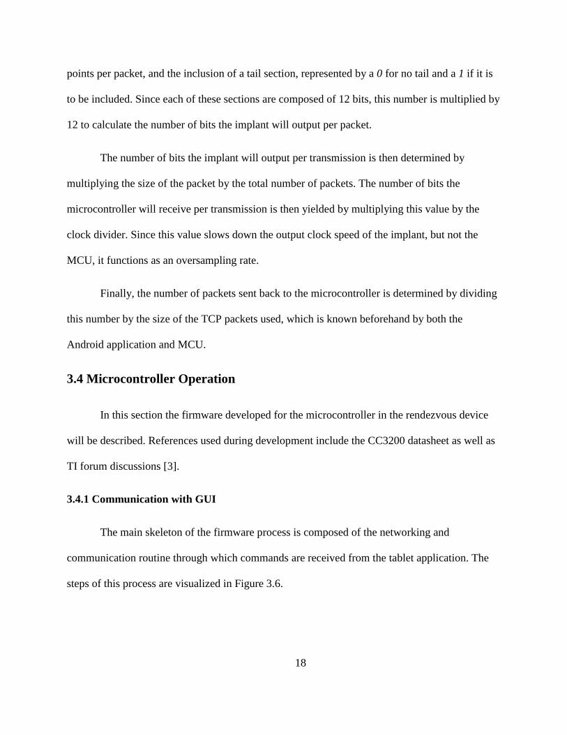
Figure 3.6: Communication Process ................................................................................. 19
Figure 3.7: Command Format ........................................................................................... 20
Figure 3.8: Command Parsing Flow ................................................................................. 21
Figure 3.9: Example Data Transfer of 0b011000110 ....................................................... 24
Figure 3.10: Example MCU Output.................................................................................. 27
Figure 3.11: Communication Between MCU and Implant ............................................... 28
Figure 3.12: Probability of Received Bit Given Oversampled Transmission .................. 28
Figure 3.13: CC3200 Receiver Setup ............................................................................... 30
Figure 3.14: Data Telemetry Flow .................................................................................... 31

viii
Figure 3.15: Correlation Filter Output. Headers are in red, Tails are in Green ................ 34
Figure 3.16: Clock Alignment on Header ......................................................................... 35
Figure 3.17: Data Extraction from Telemetry Packets ..................................................... 36
Figure 4.1: 100Hz Sine Wave ........................................................................................... 39
Figure 4.2: 100Hz Sine Wave (Zoom) .............................................................................. 40
Figure 4.3: 100Hz Triangle Wave .................................................................................... 41
Figure 4.4: 2ms Pulse at 200Hz ........................................................................................ 42
Figure 4.5:2ms Pulse at 200Hz (Zoom) ............................................................................ 43

1
Chapter 1 Introduction
As research into neuromodulation and recording has rapidly gained attention and
investment, efforts by the hardware community to provide more advanced and capable devices
have increased in tandem. This pace can be seen through the development of implantable neural
interface chips, from a state of the art 4-channel output-only stimulation chip in 2000 [1], to a
device capable of simultaneous 160-channel stimulation and 16-channel recording in 2017 [2].
Though these implants have drastically improved at an impressive pace, their integration
into neural research has been at a relatively slower rate, due to the complexity of their utilization.
While articles displaying the capabilities of these devices often provide in-vivo examples of their
efficacy, the intricacies of their experimental setup limit their use in further experiments into the
implications of certain neural activity and stimulation.
The goal of this thesis is to introduce a low-cost, modular, and simple setup with which
one of these state-of-the-art devices can be easily utilized in academic and professional research
environments. Consisting of an off-the-shelf microcontroller and an Android application capable
of being run on a wide variety of mobile devices and personal computers, it significantly lowers
the effort with which a full usable system can be built around the implant. The device developed
by Yi-Kai Lo et al. mentioned above is utilized in this solution’s development, and it is shown
that while the original paper utilized a hardwired FPGA with custom firmware for system
evaluation, full performance requirements can still be met with much lower investment.
This document elaborates on the various components used in the creation of this system,
along with functional descriptions of the algorithms and processes used to facilitate the data
telemetry functionality. Results of test runs are shown with a full data link established from the

2
front-end ADC of the neural recording device to the data’s presentation and transferal to the user,
and implications of this work on future development is discussed.

3
Chapter 2 System Overview
This chapter will give an overview of the architecture behind the neural recording system.
It consists of three main components, including the spinal implant itself, the microcontroller
‘rendezvous’ device, and the control software, run on a laptop or tablet. An example system
diagram is shown in Figure 2.1.
Figure 2.1: The Neural Recording System on a Rat Model. [2]
During experimental setup, the implant and electrode array are inserted into a biological
subject. The rendezvous device is placed within a belt strapped around the subject, powering and
communicating with the implant via inductive coils. The researcher or user of the system utilizes
a GUI application on a tablet or smartphone to control the system. This application gives full
control over the function of the implant, including controlling various parameters of neural
recording, as well as stimulation. After the user inputs the desired configuration settings, the
application packages and transmits them to the rendezvous device over a pre-established WiFi
link. The microcontroller within the rendezvous device then interprets the parameters and

4
formats them into an implant-recognizable command, which it sends over the coils. In the
recording scenario, the implant then begins to send telemetry data back over the coil to the
rendezvous device, which functions as a transceiver and relays the data back to the tablet at
speeds of up to 8Mbps. The application is then responsible for interpreting and displaying the
data to the user.
Figure 2.2: Benchtop Setup. Implant (Red), Microcontroller (Green), GUI (Blue)
Prototyping and development of the system was performed on a benchtop setup. The
implant chip was placed inside a housing that allowed access to debugging and data ports, and
the input was hard wired through a level shifter rather than transferred wirelessly via coils. This
allowed for analysis of input/output configurations independently of BER introduced by the
transfer format. The microcontroller was connected to a laptop via USB, allowing for runtime

5
debugging and output observation. The Android application was run on a laptop in order to
observe internal computation results and utilize the Android Studio debugger.
2.1 Spinal Implant
The implant used in this project was developed by Y.K. Lo et al. [2]. It is a miniaturized
SoC (system on chip), capable of both 160-channel stimulation and 16-channel recording. It is
wirelessly powered and incorporates a wireless transceiver in order to support quasi full-duplex
telemetry at 2 Mbps. The chip contains two digital controllers, the latter of which was added in
the second iteration of the device. The first controller oversees stimulation and instructs the
device to produce both anodic and cathodic pulses upon reception of commands. The second
controller, called NECSIS, is referred to as ‘the higher brain’ of the device and will remain as the
main focus for the rest of this document. This NECSIS controller is capable of both controlling
the data telemetry of the device as well as instructing the other controller to produce stimulation
periodically. This thesis will consider only the data telemetry portion.
Figure 2.3: NECSIS Controller Block Diagram [2]

6
Figure 2.3 shows the block diagram of the NECSIS controller used in this project. The
input from the coils is fed to both controllers, with a header detector on each responsible for
capturing the corresponding packets. An input select signal from the recording controller allows
the input of the stimulation controller to be rerouted, enabling internal stimulation control. In this
mode the recording controller is responsible for all functionality of the device.
When not in this mode, the controller is solely in control of data telemetry. Input
commands configure various parameters regarding the ADC, channel select multipliers, and
format of the output data. This will be discussed in greater detail in Section 3.1.
2.2 Microcontroller
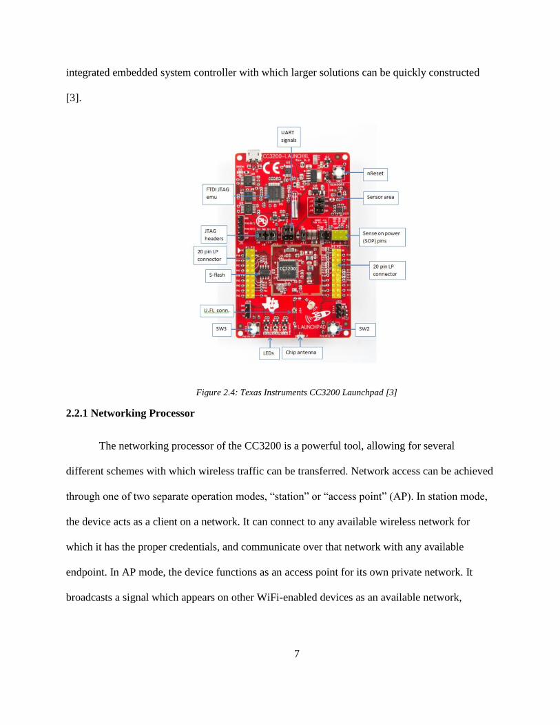
The microcontroller used in this project was the Texas Instruments SimpleLink CC3200,
shown in Figure 2.4. Containing an on-chip WiFi radio system as well as a dedicated ARM
MCU to manage the network protocol, this device allows for fully integrated internet control out
of the box. The on-board radio includes functionality enabling 802.11 b/g/n standard
communication with up to 8 simultaneous BSD sockets. Along with the WiFi subsystem, the
CC3200 leverages an ARM Cortex-M4 MCU running at 80 MHz for application control. With
on-board peripherals including UART, SPI, and I2C, it is an ideal candidate for a low-cost
7
integrated embedded system controller with which larger solutions can be quickly constructed
[3].
Figure 2.4: Texas Instruments CC3200 Launchpad [3]
2.2.1 Networking Processor
The networking processor of the CC3200 is a powerful tool, allowing for several
different schemes with which wireless traffic can be transferred. Network access can be achieved
through one of two separate operation modes, “station” or “access point” (AP). In station mode,
the device acts as a client on a network. It can connect to any available wireless network for
which it has the proper credentials, and communicate over that network with any available
endpoint. In AP mode, the device functions as an access point for its own private network. It
broadcasts a signal which appears on other WiFi-enabled devices as an available network,

8
functioning as a host for a closed network. This network includes security protocols such as
WPA2 for client authentication and secure SSL and TLS sockets using 256-bit AES encryption.
Figure 2.5: CC3200 Block Diagram [3]
Once connected to other devices, the TI SimpleLink library facilitates the creation and
usage of both TCP/IP and UDP/IP sockets. These standard BSD networking sockets are used to
transfer data bidirectionally (in the case of TCP) or unidirectionally (in the case of UDP)
between the CC3200 and any available network endpoints. The process of sending these packets
is completely offloaded from the application processer, as it is connected via the main chip bus
to the networking processor. In order to send a packet, it simply needs to transfer the relevant
data to the NWP, after which it can go back to performing other application-relevant functions.

9
2.2.2 Microcontroller Direct Memory Access Controller (µDMA)
The CC3200 MCU includes a multichannel controller that offloads data-transfer tasks
from the application processor. It provides direct routes of memory access to system peripherals
without consuming processor cycles or on-chip bus bandwidth. When preprogrammed to
repeatedly perform the same operation, data can be automatically transferred from modules such
as SPI or UART whenever the peripheral is ready. It supports multiple modes of data transfer,
including “ping-pong”, where two destination addresses can be used with one channel. This
facilitates continuous data transmission to or from a peripheral subsystem as the µDMA can
alternate between the two locations. When the first destination buffer is full, the controller sends
an interrupt to the application processor and switches to the second buffer. The application
processor can empty the first buffer while the second is being filled. This can repeat indefinitely
so that a continuous stream of input data is never broken.
2.2.3 SPI
The CC3200 contains a Serial Peripheral Interface, or SPI, subsystem that is capable of
sending and receiving data at speeds of up to 20MHz. This module was an integral part of the
neural recording system, and in order to facilitate detailed discussion on the microcontroller
process later in the paper, some background will be given on this communication standard.
SPI is a 4-wire, single-master and multi-slave communication format. One device, the
master, can talk to multiple secondary devices, the slaves. This functionality works through the
use of a separate slave select line for each secondary device. Figure 2.7 shows an example setup
of this configuration. In order to begin a transmission, the master pulls down the SS line for the

10
Figure 2.6: Sample SPI Transmission [5]
slave it wishes to communicate with. In the event of data write, the master will output data on
each falling clock edge via the Master-Out Slave-In, or MOSI line, while the slave samples on
the rising edges. In the event of a data read, the slave will output data on the Master-In Slave-Out
line while the master samples. The SS line is brought high after the data transfer to signify the
end of a transmission.
Figure 2.7: SPI Multi-Slave Mode [5]
The CC3200 supports multiple different SPI modes, including variable word lengths, no
break between successive words while acting as a slave, and 3-wire mode. In 3-wire mode, the
SS line is not used, meaning that all devices on the other three wires will be participants in every
data transfer. This is naturally desirable in the use case of a single slave. In this mode, the clock

11
edges serve as the sole catalyst for data capture or output. If performing a data read, the SPI bus
on the master will sample the MISO line on rising clock edges with no regard to the SS.
Likewise, in a data write the bus will output a bit on every falling clock edge.
2.3 Interface
The final component of the system is the Android application, which provides a GUI to
the researcher that is used both for control and data processing and visualization. The GUI allows
the user to configure the register values of the controller, which in turn determines the format of
the data output by the implant. When the GUI is used to start the data telemetry, the application
waits for and receives the data relayed back by the microcontroller. Upon the end of
transmission, it processes the data, producing an easy-to-read graph of the simultaneous channel
recordings. All this functionality will be discussed in more detail in Chapter 5.
The application was developed using Android Studio on a Windows PC. For prototyping
and development, it was run using the Android Emulator within the IDE. In this configuration,
the laptop connected to the microcontroller and served as the terminal point in the system. In
further iterations, the software was installed on a Nexus 7 Tablet, allowing for more flexibility in
experimental testing of the system.
12
Chapter 3 Operation
This chapter will cover the algorithms that facilitate control of the system as well as the
neural data pipeline. The description of the spinal implant’s operation will be given first, as this
functions as the constraints and design specifications for the rest of the system. After that, a high-
level overview of the system’s control flow will be presented, followed by deeper descriptions of
the individual components’ roles.
3.1 Implant Operation
3.1.1 Implant Output
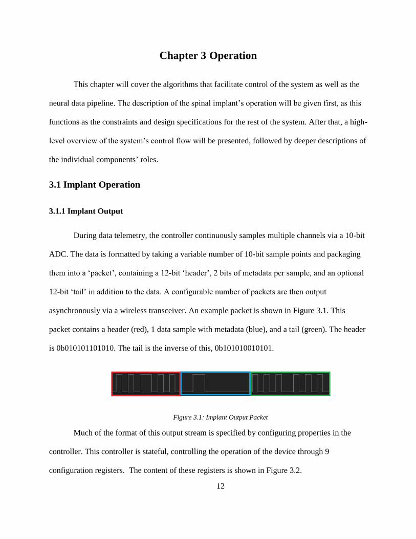
During data telemetry, the controller continuously samples multiple channels via a 10-bit
ADC. The data is formatted by taking a variable number of 10-bit sample points and packaging
them into a ‘packet’, containing a 12-bit ‘header’, 2 bits of metadata per sample, and an optional
12-bit ‘tail’ in addition to the data. A configurable number of packets are then output
asynchronously via a wireless transceiver. An example packet is shown in Figure 3.1. This
packet contains a header (red), 1 data sample with metadata (blue), and a tail (green). The header
is 0b010101101010. The tail is the inverse of this, 0b101010010101.
Figure 3.1: Implant Output Packet
Much of the format of this output stream is specified by configuring properties in the
controller. This controller is stateful, controlling the operation of the device through 9
configuration registers. The content of these registers is shown in Figure 3.2.
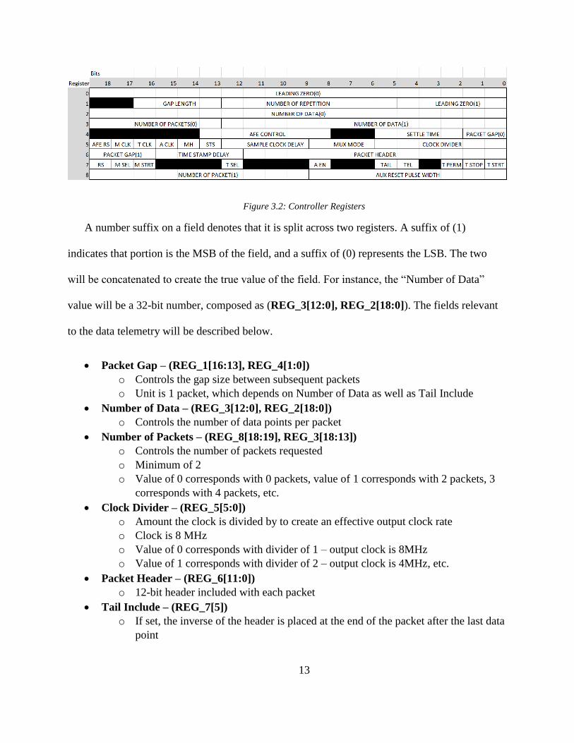
13
Figure 3.2: Controller Registers
A number suffix on a field denotes that it is split across two registers. A suffix of (1)
indicates that portion is the MSB of the field, and a suffix of (0) represents the LSB. The two
will be concatenated to create the true value of the field. For instance, the “Number of Data”
value will be a 32-bit number, composed as (REG_3[12:0], REG_2[18:0]). The fields relevant
to the data telemetry will be described below.
• Packet Gap – (REG_1[16:13], REG_4[1:0])
o Controls the gap size between subsequent packets
o Unit is 1 packet, which depends on Number of Data as well as Tail Include
• Number of Data – (REG_3[12:0], REG_2[18:0])
o Controls the number of data points per packet
• Number of Packets – (REG_8[18:19], REG_3[18:13])
o Controls the number of packets requested
o Minimum of 2
o Value of 0 corresponds with 0 packets, value of 1 corresponds with 2 packets, 3
corresponds with 4 packets, etc.
• Clock Divider – (REG_5[5:0])
o Amount the clock is divided by to create an effective output clock rate
o Clock is 8 MHz
o Value of 0 corresponds with divider of 1 – output clock is 8MHz
o Value of 1 corresponds with divider of 2 – output clock is 4MHz, etc.
• Packet Header – (REG_6[11:0])
o 12-bit header included with each packet
• Tail Include – (REG_7[5])
o If set, the inverse of the header is placed at the end of the packet after the last data
point

14
Figure 3.3: Input Packet Structure
• Telemetry Start – (REG_7[4])
o A transition from 0 to 1 starts the data output
o Register must be set to 0 before being set to 1 in between each telemetry session
in order to start the next one.
3.1.2 Implant Input
The chip expects a specific input packet structure to fill out the register fields. The packet
structure is shown in Figure 3.3 below.
The packet consists of 5 fields, each of which are 19 bits, for a total of 95 bits to set a
register. In addition, if at any point the header marker is present in the data being sent after the
header, a “reverse header marker” consisting of the bitwise inverse of the header is placed
immediately following to let the chip know that it is not the beginning of a transmission.
The fields are described as follows:
• Header Marker
o 0b0000001101010101011
o Reverse Header Marker
▪ 0b1111110010101010100
• Register Address
o 0b01000000000XXXX0010
o The X’s correspond with the address of the register being filled
o The values 0001-1001 correspond with registers 0-8, respectively
• Register Value
o The desired 19-bit value to be placed in the register
• Checksum & CRC
o For packet validation

15
3.2 Control Flow
Figure 3.4: Control Flow of System
Figure 3.4 shows a high-level overview of the full operation of the neural recording
system. A run is initiated with the user inputting the configuration parameters representing the
desired telemetry operation into the tablet. When these values are input, the transmission is sent
to the microcontroller via Wi-Fi.
Upon reception of the transmission from the tablet, the microcontroller parses the data
stream. It packages the desired register values into packets consisting of a header, register
address, value, checksum, and CRC, as shown in Figure 3.3. This output is then synchronously
transmitted to the implant.
As discussed in Section 3.1.1, the telemetry operation is started by the “Telemetry Start”
register field being flipped from 0 to 1. Both the tablet and microcontroller are programmed to

16
check this field, and upon this behavior prepare to perform the reverse link data transfer. After
sending the transmission to the implant, the microcontroller begins continuously sampling the
output stream of the neural recording device. As the MCU samples, it relays the data via TCP/IP
to the tablet. Upon the end of the data output from the implant, it closes the socket to which the
tablet is connected, signaling the end of a transmission. The tablet then processes the data,
converting the raw bit stream into base-10 integer data points, which it then represents to the user
in the form of a time series line graph.
3.3 Application Control
Figure 3.5: Telemetry Configuration
Figure 3.5 shows the interface presented to the user when they wish to configure the
telemetry output. Relevant fields regarding the output format of the data are shown on the left,
under Telemetry Control. The right image shows the same screen after having been scrolled
17
down further. Important fields for telemetry in this view include MUX Mode, which controls the
electrode channels sampled, and Clock Divider which controls the sampling and output speed of
the implant.
When the user is done inputting the desired values, they scroll to the bottom of the screen
and press a button labeled Start Telemetry. This calls a function within the application that then
formats the configuration data into the appropriate register values. First, 9 32-bit integers are
created which represent the 9 registers in the system. Since they are 19-bit registers, the top 13
bits of each integer will remain zero. Through bitwise operations, the input values are shifted and
concatenated to construct the register values.
The application also communicates the desired number of TCP packets for the
microcontroller to relay back to the tablet. This is necessary to indicate to the MCU due to the
implant having no “end of transmission” sequence. Since the microcontroller samples at a
constant rate of 8 MHz, the number of data points, number of packets, tail include, and clock
speed can be used to calculate the number of raw bits that will be needed to capture the entire
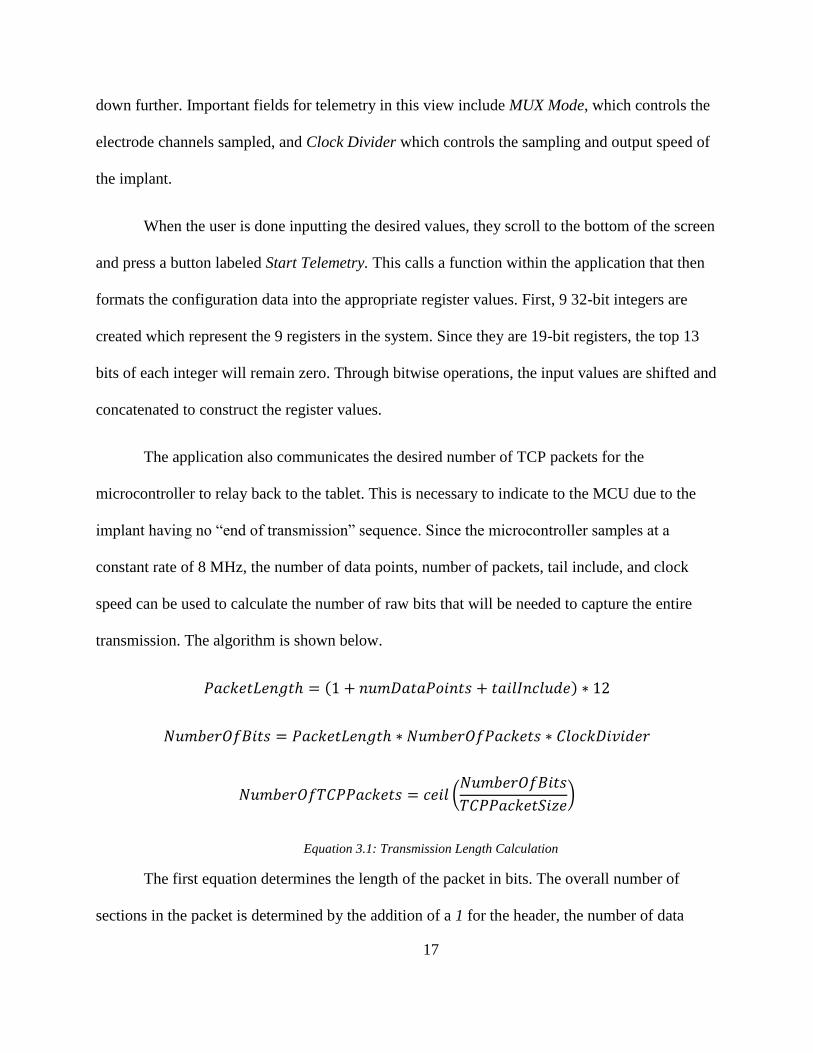
transmission. The algorithm is shown below.
𝑃𝑎𝑐𝑘𝑒𝑡𝐿𝑒𝑛𝑔𝑡ℎ = (1 + 𝑛𝑢𝑚𝐷𝑎𝑡𝑎𝑃𝑜𝑖𝑛𝑡𝑠 + 𝑡𝑎𝑖𝑙𝐼𝑛𝑐𝑙𝑢𝑑𝑒) ∗ 12
𝑁𝑢𝑚𝑏𝑒𝑟𝑂𝑓𝐵𝑖𝑡𝑠 = 𝑃𝑎𝑐𝑘𝑒𝑡𝐿𝑒𝑛𝑔𝑡ℎ ∗ 𝑁𝑢𝑚𝑏𝑒𝑟𝑂𝑓𝑃𝑎𝑐𝑘𝑒𝑡𝑠 ∗ 𝐶𝑙𝑜𝑐𝑘𝐷𝑖𝑣𝑖𝑑𝑒𝑟
𝑁𝑢𝑚𝑏𝑒𝑟𝑂𝑓𝑇𝐶𝑃𝑃𝑎𝑐𝑘𝑒𝑡𝑠 = 𝑐𝑒𝑖𝑙 (𝑁𝑢𝑚𝑏𝑒𝑟𝑂𝑓𝐵𝑖𝑡𝑠
𝑇𝐶𝑃𝑃𝑎𝑐𝑘𝑒𝑡𝑆𝑖𝑧𝑒)
Equation 3.1: Transmission Length Calculation
The first equation determines the length of the packet in bits. The overall number of
sections in the packet is determined by the addition of a 1 for the header, the number of data
18
points per packet, and the inclusion of a tail section, represented by a 0 for no tail and a 1 if it is
to be included. Since each of these sections are composed of 12 bits, this number is multiplied by
12 to calculate the number of bits the implant will output per packet.
The number of bits the implant will output per transmission is then determined by
multiplying the size of the packet by the total number of packets. The number of bits the
microcontroller will receive per transmission is then yielded by multiplying this value by the
clock divider. Since this value slows down the output clock speed of the implant, but not the
MCU, it functions as an oversampling rate.
Finally, the number of packets sent back to the microcontroller is determined by dividing
this number by the size of the TCP packets used, which is known beforehand by both the
Android application and MCU.
3.4 Microcontroller Operation
In this section the firmware developed for the microcontroller in the rendezvous device
will be described. References used during development include the CC3200 datasheet as well as
TI forum discussions [3].
3.4.1 Communication with GUI
The main skeleton of the firmware process is composed of the networking and
communication routine through which commands are received from the tablet application. The
steps of this process are visualized in Figure 3.6.
19
Figure 3.6: Communication Process
On boot, the program begins by initializing all necessary peripherals needed for
execution of the telemetry process. These include GPIO pins utilized for outputting commands,
an SPI bus to receive data from the implant, a UART bus for USB debugging purposes, and

20
several timers used in various time critical portions of the application. The boot sequence also
includes sending the startup signal to the networking processor, which is subsequently used for
all wireless communication.
The networking processor is configured to operate in AP mode, described in Section 2.2.
On boot, it takes the hardcoded network name and password and begins broadcasting a WiFi
network. The CC3200 networking subsystems include an interrupt routine that sets a global
variable upon client connection. The main processor intermittently sleeps until this connection is
observed, saving power while the application processor is not needed.
Upon client connection, the application firmware opens a TCP server socket and awaits a
transmission from the client. It follows the same sleep and check protocol to ensure low power
usage while awaiting a notification from the network processor that a command has been
received.
3.4.2 Command Parsing
The data format used for communication between the application and the microcontroller
was chosen based on ease of use and simplicity of development and debugging. It is composed
of a single string containing all necessary parameter specifications for data telemetry.
𝑛𝑟0; 𝑟1; 𝑟2; 𝑟3; 𝑟4; 𝑟5; 𝑟6; 𝑟7; 𝑟8; 𝑝
Figure 3.7: Command Format
Figure 3.7 shows the command format. This is received from the TCP socket by the
application and is stored in a buffer of characters. The program then iterates through the buffer to
parse and interpret the string. An n character represents the start of a NECSIS command.

21
Following this, an rx value represents the integer value for register x. The register values are
followed by the packet count, represented here as p. The string is post fixed by a space in order
to signify the end of the command. Figure 3.8 shows the parsing flow.
Figure 3.8: Command Parsing Flow
After the command is parsed, the 9 register values have been stored in memory in integer
form. The application then formats these numbers into the appropriate packets for transmission
to the implant.
3.4.3 Input Packaging
Before the register values can be transmitted to the implant, they must be inserted into
controller-readable packets, the structure of which was described in Section 3.1.2. This section
will give an overview of how this is accomplished in the microcontroller.

22
The firmware has a statically allocated buffer of characters with size 150B. This will
serve as a contiguous block of memory where the binary output can be recorded without gaps,
which is fundamental for correct functionality of the output process, described in the next
section. In order to format the data, the application iterates through the 9 register values and sets
the correct output buffer bit by bit. This is done through the use of a global bit_index to indicate
the desired bit, along with a mask that is constructed from the data. A running tracker of the
previous 19 bits is kept in memory, and if at any point the header marker is present in the data a
reverse header marker is added. The pseudo code for the process is shown below.
Algorithm 1 Pseudo Code for Data Format Creation
bit_index = 0
for i = 0 → 9 do
OutputData[bit_index:bit_index+18] = HEADER
bit_index += 19
start_index = bit_index
OutputData[bit_index:bit_index+18] = ADDRESS[i]
bit_index += 19
OutputData[bit_index:bit_index+18] = register_value[i]
bit_index += 19
OutputData[bit_index:bit_index+18] = Checksum(OutputData[start_index:bit_index])
bit_index += 19
OutputData[bit_index:bit_index+18] = CRC(OutputData[start_index:bit_index])
end for

23
The 19-bit checksum code is calculated by adding the entire data portion together on a
19-bit basis. This value is then negated and added to the end of the data packet. Following this, a
CRC code is generated on a bit-by-bit basis and added to the end of the packet. It uses the 20-bit
polynomial shown below in Equation 3.2.
𝑥20 + 𝑥4 + 𝑥1 + 1
Equation 3.2: 20-bit CRC Calculation
3.4.4 Output
The output function is responsible for sending the formatted data to the spinal implant.
Due to the requirements of the spinal implant input, along with the limitations of the CC3200,
this application used the MCU’s peripherals in an unusual way to get the data across.
The implant requires an input line and clock line at 2Mbps and 2MHz respectively, with
an unbroken stream of data. These requirements make the use of any MCU communication
standard unfeasible to transfer the command. SPI has breaks in the data and clock signals, which
the implant would not be able to interpret. The I2C standard also includes breaks in the data and
clock, along with requiring an ACK bit that the implant will not send. In addition to this, the I2C
bus on the CC3200 has a max speed of 400kbps, which is far too slow for this application. The
final communication standard available on the CC3200 is UART, which would not work as it has
no clock line and includes communication standard bits within the data line.
The end implementation of the output function utilized a GPIO pin that was repeatedly
toggled to transmit the data, paired with an in-phase hardware timer to output the 2MHz clock
signal. Timing the GPIO proved to be difficult, as the ARM Cortex-M4’s internal interrupt
routine was only capable of switching an output pin at a rate of 200kbps. To get around this, the
program manually toggles the pin without exiting the current function. This eliminates the
24
inherent time penalty present in context switches, but introduces the difficulty of reliably
outputting the bits at the correct frequency and phase.
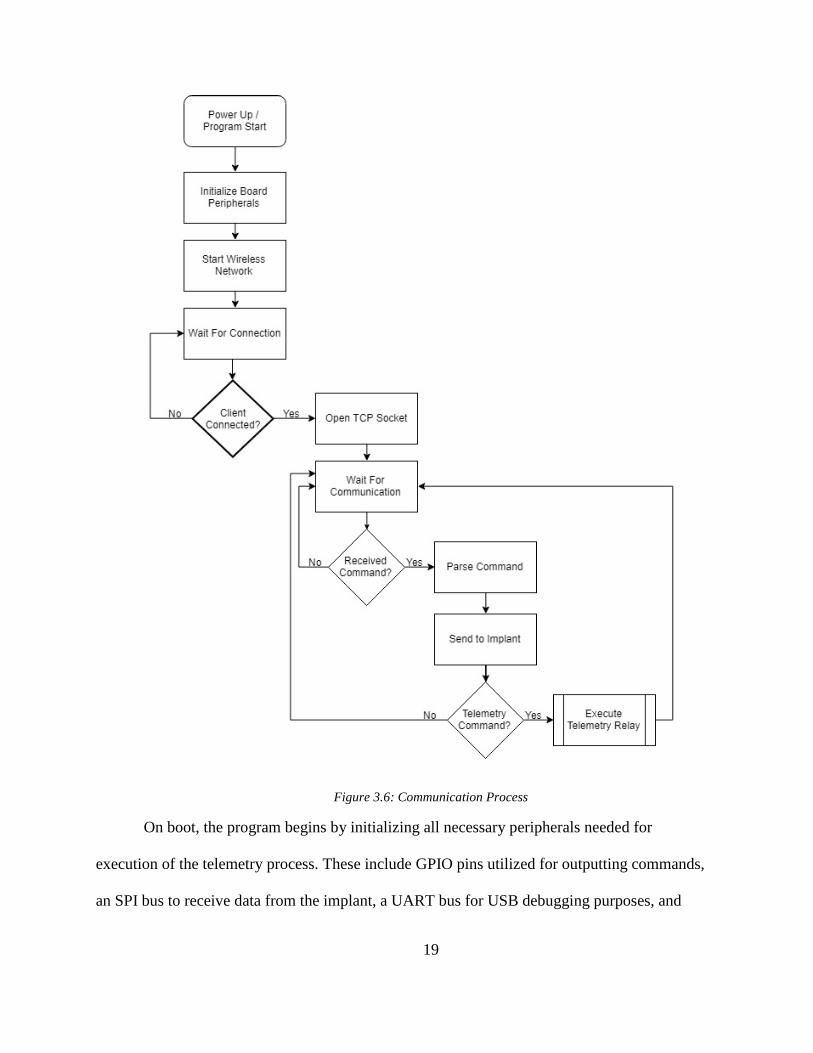
Figure 3.9: Example Data Transfer of 0b011000110
Figure 3.9 shows an example data transfer the implant is expecting. The receiver latches
the data bits on a rising clock edge, requiring the data logic shifts to be on the falling clock edge.
With a clock speed of 2MHz, these transitions need to happen at multiples of 50µs. The ARM
Cortex-M4 runs at a speed of 80MHz, yielding a single cycle time of 12.5ns. From this it can be
calculated that the application processor should toggle a bit every 40 cycles.
Algorithm 2 shows the pseudo code for the output routine. First, we will focus on the pin
toggling present in the two for loops. The ARM Cortex-M4 reference manual [7] was used in
conjunction with the assembler code produced by the library to calculate the number of cycle
delays needed in order to toggle the pin at exactly 2MHz. From the assembly code instructions,
each loop iteration itself consisted of an add, compare, and branch. The add and compare take a
constant one cycle each, and the branch takes a variable number of cycles. It was observed
empirically that in this routine that a loop branch would take a single cycle consistently, but two
loop branches would take a variable number of cycles. In order to avoid this case, the eighth bit
of each byte was removed from the inner loop.

25
Algorithm 2 Pseudo Code for Data Output
while timer ≠ desired range do
nothing
end while
for i = 0 → numBytes do
for j = 0 → 6 do
GPIO_pin = data[i][j]
no-op x 26
end for
no-op x 3
GPIO_pin = data[i][7]
no-op x 20
end for
The ARM library provides direct access to the hardware register, which allows you to
toggle the pin by storing a register to a memory address. Using any sort of branching to choose
the correct pin value would result in a variable number of cycles and was avoided by using
bitwise logic to return the proper 0 or 1. From the assembly code, loading the data byte,
performing the bitwise logic, and storing it to memory at the address of the GPIO took a total of
11 cycles.

26
Operation Cycle Count
Loop 3
Pin Toggle 11
No-op 1
Table 3.1: Cycle Counts
The operation of toggling the pin and performing a loop increment resulted in a cycle
cost of 14. Thus, 26 no-ops needed to be added to the inside loop to produce an even 40 cycles
per iteration, resulting in 2MHz. The last iteration of the loop performed the correct branch
prediction and was observed to have a zero-cycle penalty on exit. This required an extra 3 no-ops
prior to the eighth bit. The outer loop in combination with starting the inner loop again took 9
cycles, due to an additional load and initialization of the j iterator, resulting in a delay of only 20
cycles needed before the next pin toggle iteration. This routine proved capable of consistently
outputting the bits at a 40-cycle interval, confirmed both empirically as well as by the assembly
code.
For the clock output, a hardware timer was set to output PWM from an external pin on
the CC3200. It decrements from 39 to 0 (40 cycles), with a check set to 19 to flip the output.
This results in a 50% duty PWM signal at 2MHz, accomplishing the desired clock signal.
However, since an interrupt set on the same timer would introduce an unacceptable amount of
latency, the GPIO data output must be manually aligned with the clock signal. This was done by
introducing a while loop prior to the output process that waits until the clock is in a desirable
range prior to starting the output.
27
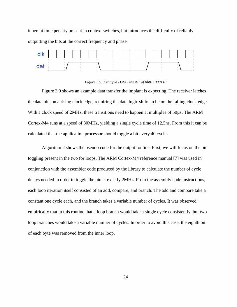
Figure 3.10: Example MCU Output
3.4.5 Telemetry
The data telemetry process introduced additional difficulty when compared to the output
routine. The design of the wireless transceiver on the spinal implant utilizes two different
communication schemes in order to reduce interference between the transmitted and received
data, as well as to reduce power usage on the implant side. The differential phase-shift keying
used for microcontroller transmission allows for the use of a clock, utilized in the modulation of
the data at the wireless transmitter. The demodulation device on the implant then recovers the
clock signal from the transmission, allowing for correct latching of the data bits when received
by the digital controller. Data telemetry in the reverse direction uses load shift-keying, which
does not allow a simple method with which to recover the clock data from the modulated signal.
Thus, the signal received by the microcontroller is simply an asynchronous bit stream with no
28
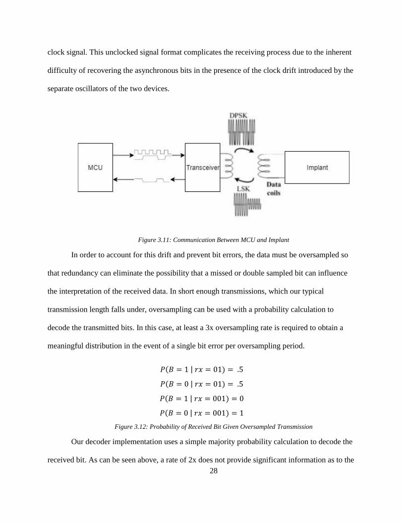
clock signal. This unclocked signal format complicates the receiving process due to the inherent
difficulty of recovering the asynchronous bits in the presence of the clock drift introduced by the
separate oscillators of the two devices.
Figure 3.11: Communication Between MCU and Implant
In order to account for this drift and prevent bit errors, the data must be oversampled so
that redundancy can eliminate the possibility that a missed or double sampled bit can influence
the interpretation of the received data. In short enough transmissions, which our typical
transmission length falls under, oversampling can be used with a probability calculation to
decode the transmitted bits. In this case, at least a 3x oversampling rate is required to obtain a
meaningful distribution in the event of a single bit error per oversampling period.
𝑃(𝐵 = 1 | 𝑟𝑥 = 01) = .5
𝑃(𝐵 = 0 | 𝑟𝑥 = 01) = .5
𝑃(𝐵 = 1 | 𝑟𝑥 = 001) = 0
𝑃(𝐵 = 0 | 𝑟𝑥 = 001) = 1
Figure 3.12: Probability of Received Bit Given Oversampled Transmission
Our decoder implementation uses a simple majority probability calculation to decode the
received bit. As can be seen above, a rate of 2x does not provide significant information as to the

29
received bit. A rate of at least 3x is needed to correct a bit error in a given oversampling period.
Our implementation uses a rate of 4x to provide further redundancy. The decoding will be
discussed further in the next section.
An oversampling rate of 4x on a 2MHz stream of data requires a receiver running at
8MHz on the microcontroller. No microcontroller peripheral subsystem is capable of
continuously asynchronously sampling a bit stream at that speed. As discussed in the Section
3.1.1, the interrupt routine does not execute quickly enough to reach these speeds. A similar
schema to the output data transfer could be used, however that routine demands the full attention
of the application processor in order to correctly time the bit stream. This is not suitable for the
reverse link, as the amount of data being transferred far exceeds the memory available on the
microcontroller. Thus, the application processor must be simultaneously sending data to the
tablet as it is received in order to not overflow the on-board memory.
The solution to recovering this data line was accomplished through the use of the
synchronous SPI bus, a hardware timer, and the µDMA controller. Recall from Section 2.2.3 that
the SPI system on the CC3200 is capable of running at speeds of up to 20MHz. While in slave
mode it can receive data with no breaks in between word lengths, and while in 3-pin mode data
capture is triggered solely by a rising clock edge. Running a hardware timer in 50% PWM mode
at 8MHz and feeding it into the CLK of the SPI bus while in slave 3-pin mode allows for
continuous sampling of the data line at the desired rate. Figure 3.13 shows the wiring setup for
reception.
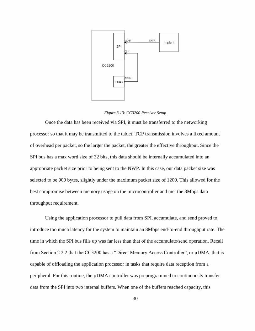
30
Figure 3.13: CC3200 Receiver Setup
Once the data has been received via SPI, it must be transferred to the networking
processor so that it may be transmitted to the tablet. TCP transmission involves a fixed amount
of overhead per packet, so the larger the packet, the greater the effective throughput. Since the
SPI bus has a max word size of 32 bits, this data should be internally accumulated into an
appropriate packet size prior to being sent to the NWP. In this case, our data packet size was
selected to be 900 bytes, slightly under the maximum packet size of 1200. This allowed for the
best compromise between memory usage on the microcontroller and met the 8Mbps data
throughput requirement.
Using the application processor to pull data from SPI, accumulate, and send proved to
introduce too much latency for the system to maintain an 8Mbps end-to-end throughput rate. The
time in which the SPI bus fills up was far less than that of the accumulate/send operation. Recall
from Section 2.2.2 that the CC3200 has a “Direct Memory Access Controller”, or µDMA, that is
capable of offloading the application processor in tasks that require data reception from a
peripheral. For this routine, the µDMA controller was preprogrammed to continuously transfer
data from the SPI into two internal buffers. When one of the buffers reached capacity, this
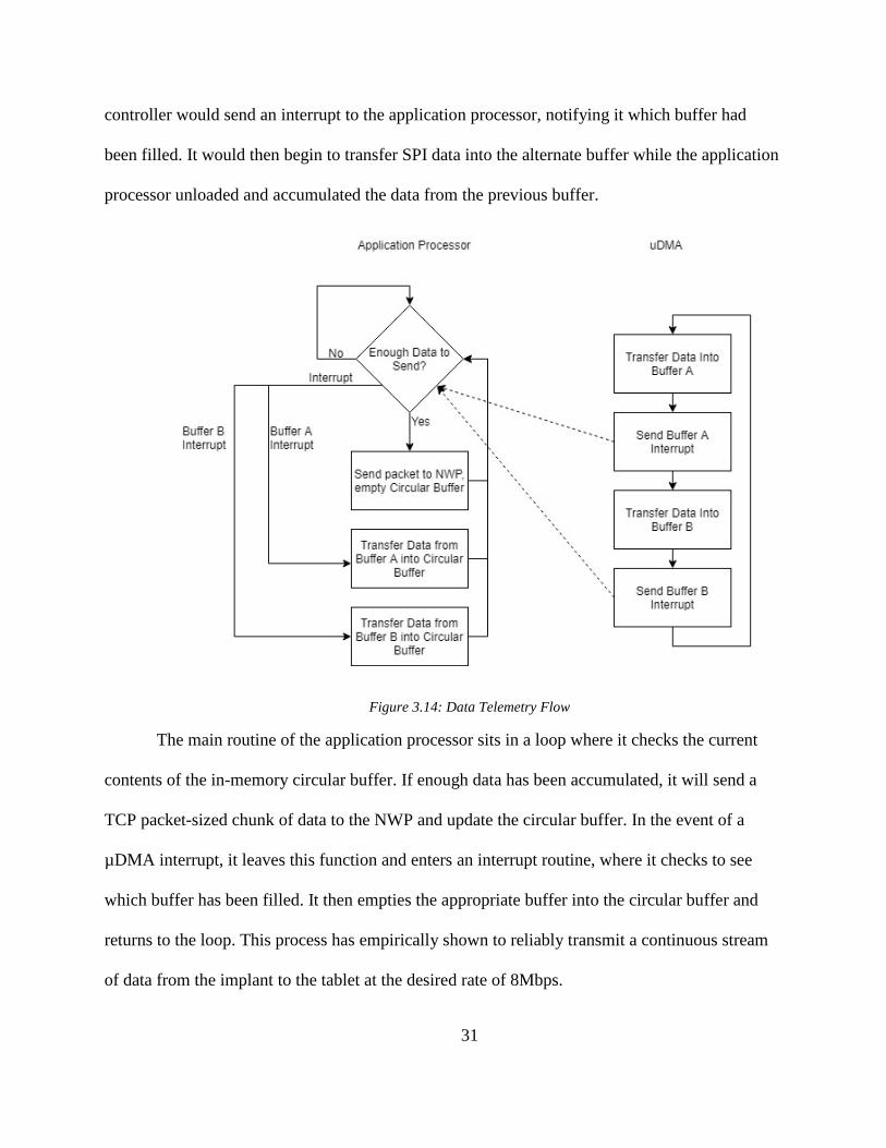
31
controller would send an interrupt to the application processor, notifying it which buffer had
been filled. It would then begin to transfer SPI data into the alternate buffer while the application
processor unloaded and accumulated the data from the previous buffer.
Figure 3.14: Data Telemetry Flow
The main routine of the application processor sits in a loop where it checks the current
contents of the in-memory circular buffer. If enough data has been accumulated, it will send a
TCP packet-sized chunk of data to the NWP and update the circular buffer. In the event of a
µDMA interrupt, it leaves this function and enters an interrupt routine, where it checks to see
which buffer has been filled. It then empties the appropriate buffer into the circular buffer and
returns to the loop. This process has empirically shown to reliably transmit a continuous stream
of data from the implant to the tablet at the desired rate of 8Mbps.

32
3.3 Data Processing
3.3.1 Downsampling & Extraction
Once the tablet has received the stream of oversampled data it must be processed in order
to display meaningful results to the user. The first step in this process is converting the signal to
the appropriate sampling rate. Recall from Section 3.3 that the clock divider setting functions as
an oversampling rate, as it slows down the output speed of the implant but not the
microcontroller’s sampling rate. This rate can be used to determine with what factor the
transmission must be downsampled to reach the true rate. However, due to errors introduced by
clock drift we must maintain at least a 4x oversampling rate for our majority decoder to function
properly. To achieve this, the process begins by downsampling the signal at a rate equal to the
true oversampling rate over the desired.
𝐷𝑆𝑅𝑎𝑡𝑒 = 𝑂𝑣𝑒𝑟𝑠𝑎𝑚𝑝𝑙𝑖𝑛𝑔 𝑅𝑎𝑡𝑒
4
Equation 3.3: Effective Downsampling Rate
Once the transmission is at the appropriate rate, the binary stream is checked for
telemetry packets. Packet existence and location can be found through the detection of the
“header marker” input in the NECSIS telemetry setting screen, shown in Section 3.3. This header
is used with a fast and simple convolutional filter to locate matching patterns within the signal.
For a convolutional filter to be useful and not yield false positives, the binary 0/1 scheme must
be translated to represent symbols as ±1. This causes correlation between 0 bits in the header and
transmission to contribute to the overall filter output, rather than only correlation between 1’s.
Though the header is known, its actual form does not exist as expected within the transmission,
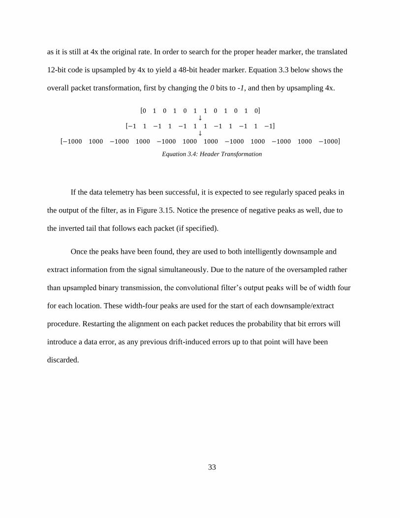
33
as it is still at 4x the original rate. In order to search for the proper header marker, the translated
12-bit code is upsampled by 4x to yield a 48-bit header marker. Equation 3.3 below shows the
overall packet transformation, first by changing the 0 bits to -1, and then by upsampling 4x.
[0 1 0 1 0 1 1 0 1 0 1 0] ↓
[−1 1 −1 1 −1 1 1 −1 1 −1 1 −1] ↓
[−1000 1000 −1000 1000 −1000 1000 1000 −1000 1000 −1000 1000 −1000]
Equation 3.4: Header Transformation
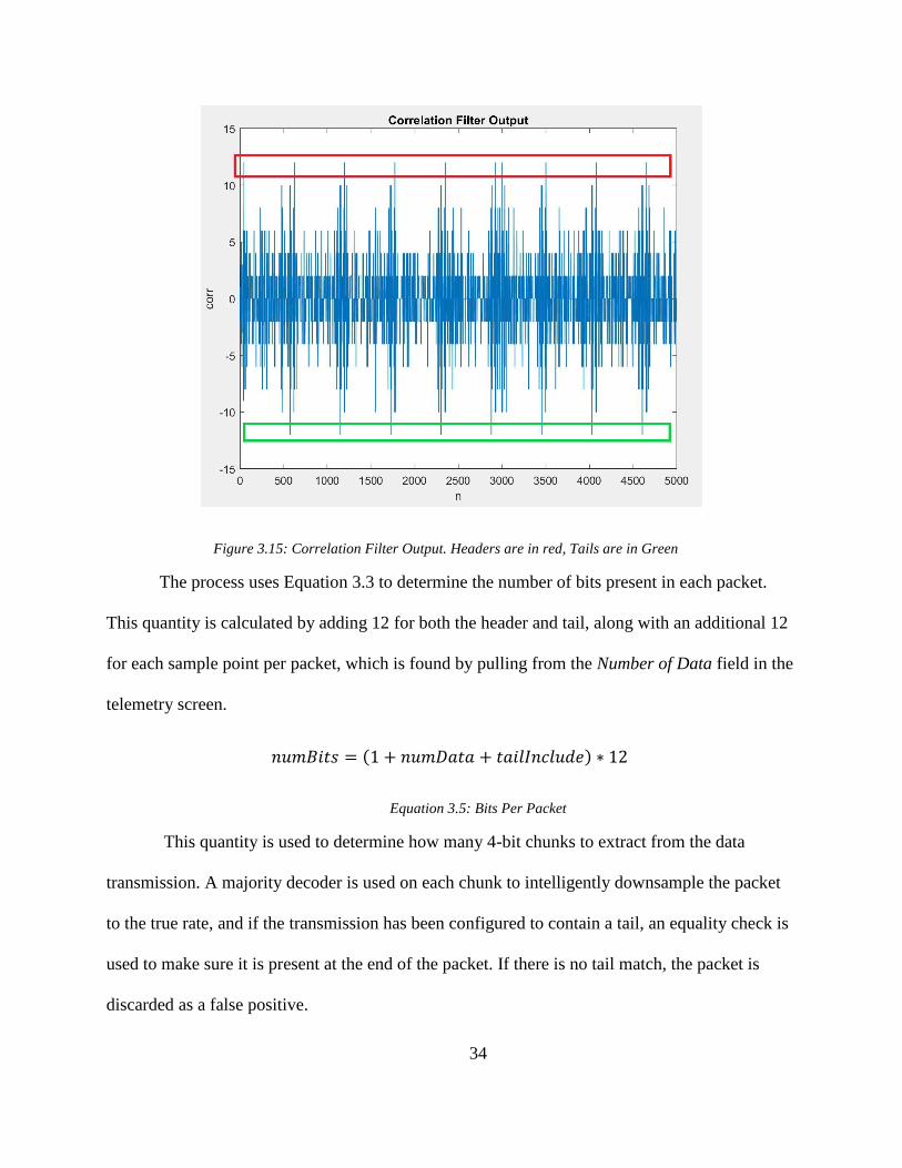
If the data telemetry has been successful, it is expected to see regularly spaced peaks in
the output of the filter, as in Figure 3.15. Notice the presence of negative peaks as well, due to
the inverted tail that follows each packet (if specified).
Once the peaks have been found, they are used to both intelligently downsample and
extract information from the signal simultaneously. Due to the nature of the oversampled rather
than upsampled binary transmission, the convolutional filter’s output peaks will be of width four
for each location. These width-four peaks are used for the start of each downsample/extract
procedure. Restarting the alignment on each packet reduces the probability that bit errors will
introduce a data error, as any previous drift-induced errors up to that point will have been
discarded.
34
Figure 3.15: Correlation Filter Output. Headers are in red, Tails are in Green
The process uses Equation 3.3 to determine the number of bits present in each packet.
This quantity is calculated by adding 12 for both the header and tail, along with an additional 12
for each sample point per packet, which is found by pulling from the Number of Data field in the
telemetry screen.
𝑛𝑢𝑚𝐵𝑖𝑡𝑠 = (1 + 𝑛𝑢𝑚𝐷𝑎𝑡𝑎 + 𝑡𝑎𝑖𝑙𝐼𝑛𝑐𝑙𝑢𝑑𝑒) ∗ 12
Equation 3.5: Bits Per Packet
This quantity is used to determine how many 4-bit chunks to extract from the data
transmission. A majority decoder is used on each chunk to intelligently downsample the packet
to the true rate, and if the transmission has been configured to contain a tail, an equality check is
used to make sure it is present at the end of the packet. If there is no tail match, the packet is
discarded as a false positive.

35
Figure 3.16: Clock Alignment on Header
Now that the packets have been extracted from the transmission, the actual ADC sample
points must be pulled out of each packet and arranged in the correct channel order. Due to
current limitations with the device, the implant is configured to always relay channels 0-7
sequentially. There is no metadata present within the signal to demarcate the channel number
that a sample is coming from, so it must be tracked through cyclical appearance rather than
analytically through a bit field. Configuring the implant to relay channels 0-7 along with a data
number that is a multiple of 8 allows us to observe 1 sample point per channel per packet. The
data between the header and tail is subdivided into 12-bit chunks, and the last 10 bits of each are
placed into their respective column in an 𝑛 × 8 × 10 matrix, discarding the two metadata bits.
The matrix is then processed to convert the 10-bit binary numbers to integers and placed into an
𝑛 × 8 matrix of integer sample data.

36
Figure 3.17: Data Extraction from Telemetry Packets
Once this process has been completed, the data is passed off to a graphing function,
described in the next section. A setting within the app allows the user to determine whether to
save the data onto the devices local drive in .CSV format, should they want to perform further
analysis.
3.3.2 Data Display
The Android application uses the package AChartEngine to create meaningful and legible
graphs to display the data to the user [6]. This software allows the programmer to preconfigure
multiple parameters regarding the physical display of the graph, optimizing it to convey the
appropriate data. In the hands of the user, it offers multiple convenient features to analyze the
data, including dynamic axis scales, zooming, and panning.
For our purpose the graph was preconfigured to display a set Y-range of 0-1024, per the
dynamic range of the 10-bit ADC. The X-axis range was set to be dynamic to fit as large or small

37
an amount of data as needed. The X-axis scale was set to display time, based on the frequency of
the implant clock and the clock divider parameter supplied during the initiation of telemetry.

38
Chapter 4 Results
To produce results for this section, the chip was utilized in the benchtop setup shown in
Figure 2.2. The Android application was run in the Android Studio Emulator in order to facilitate
clean screenshots and data gathering. A signal generator was run to the ADC input of the spinal
implant chip, providing both the input signal to sample as well as the clock to control the ADC
switching between channels. In the real experimental setup, the ADC clock input would be
generated internally, rather than externally. Due to the current debug setup of the implant chip,
this connection was not established and forced an external signal to be fed into the device. This
resulted in phase misalignment between the telemetry and ADC clocks, which is noticeable in
some of the examples below. Previous testing has shown that this is a nonissue during normal
operation of the implant. The ADC was configured to sample from 0 to 1.8V, and the readings
are shown on the base-10 10-bit integer scale of the ADC output, ranging from 0 (0V) to
210=1024 (1.8V).

39
Figure 4.1: 100Hz Sine Wave
The first example shown in Figure 4.1 is a 100MHz sine wave, sampled at 83.3kHz with
a 1MHz telemetry clock. This was tested as a baseline with which to ensure the reverse data
transfer was functioning correctly. It can be seen that the readings are consistent among all 8
overlapping channels, and the upper and lower bounds are at constant voltage. The X scale in the
graph shown is on the order of seconds, displaying a total of ~4ms of data.

40
Figure 4.2: 100Hz Sine Wave (Zoom)
Figure 4.2 shows the same sine wave, zoomed in to show the individual channels. The
noise present is on the order of 80mV, resulting from the analog front end of the device.

41
Figure 4.3: 100Hz Triangle Wave
Figure 4.3 shows a 100Hz triangle wave sampled in the same method as before. The
corners show that the device appropriately samples high frequency content, and that no
smoothing filter was used to round out noise.
42
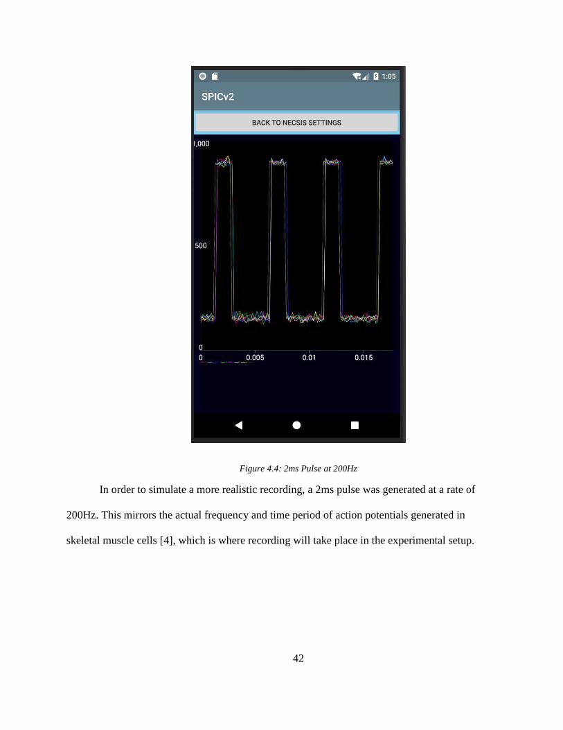
Figure 4.4: 2ms Pulse at 200Hz
In order to simulate a more realistic recording, a 2ms pulse was generated at a rate of
200Hz. This mirrors the actual frequency and time period of action potentials generated in
skeletal muscle cells [4], which is where recording will take place in the experimental setup.
43
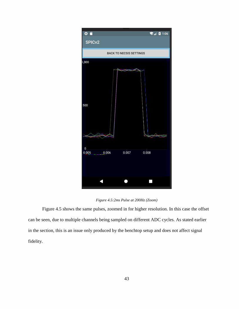
Figure 4.5:2ms Pulse at 200Hz (Zoom)
Figure 4.5 shows the same pulses, zoomed in for higher resolution. In this case the offset
can be seen, due to multiple channels being sampled on different ADC cycles. As stated earlier
in the section, this is an issue only produced by the benchtop setup and does not affect signal
fidelity.

44
Chapter 5 Conclusions and Future Work
This thesis has shown the possibility of using a state of the art implantable neural
recording device within a relatively low-cost and functional end-to-end system. Capable of
controlling telemetry and streaming neural data back at the full speed offered by the implant, this
solution offers researchers a simple and usable method of integrating novel technology into their
neural applications.
In future iterations of this device the application should be updated to display data in real-
time to the user, updating as the microcontroller sends more data to the receiver. This would
allow for analysis of how certain stimulation affects the muscular response immediately while
performing the experiment, removing the guesswork from aligning separate timeframes.
In addition, the spinal implant could be improved to make the creation of a rendezvous
device more simplistic, improving data rates and reducing development time. The inclusion of
circuitry to facilitate a “self-clocking” asynchronous signal such as Manchester Encoding could
be paired with the appropriate decoding circuitry on the rendezvous side, producing in-phase
clock and data signals [8]. This would remove both the need for drastic oversampling as well as
the SPI-rigging mechanism introduced in this paper.
Finally, as suggested in other papers by this lab [2], the development of a real-time
closed-loop system to process the neural recording and produce the appropriate stimulation
would result in a full system capable of dynamically controlling muscle stimulation. This would
pave the way for full rehabilitation devices capable of restoring lower body function to those
who have lost it.

45
Chapter 6 References
1. Gunnar Gudneson, Erik Bruun, Morten Haugland. “A Chip for an Implantable Neural
Stimulator”, Analog Integrated Circuits and Signal Processing, Issue 1, pp 81-89, 2000.
2. Y.-K. Lo, Y.-C. Kuan, S. Culaclii, B. Kim, P.-M. Wang, C.-W. Chang, et al., “A Fully
Integrated Wireless SoC for Motor Function Recovery after Spinal Cord Injury,” IEEE
Transactions on Biomedical Circuits and Systems, vol. 11, pp. 497-509, 2017.
3. Texas Instruments. “CC3200 SimpleLink™ Wi-Fi® and Internet-of-Things Solution, a
Single-Chip Wireless MCU Datasheet.” Texas Instruments, Feb. 2015, www.ti.com.
4. Ganong, William F. Review of Medical Physiology. Appleton & Lange, 1991.
5. Grusin, Mike. “Serial Peripheral Interface (SPI).” SparkFun, 2018,
learn.sparkfun.com/tutorials/serial-peripheral-interface-spi/.
6. The 4ViewSoft Company. “AChartEngine.” 2017, http://www.achartengine.org/
7. ARM Limited. “Cortex-M4 Technical Reference Manual.” ARM Infocenter, 2010,
infocenter.arm.com/help/topic/com.arm.doc.ddi0439b/DDI0439B_cortex_m4_r0p0_trm.
8. Tanenbaum, Andrew S. Computer Networks (4th ed.). Prentice Hall. pp. 274–275, 2002.
Related Documents