UC Berkeley UC Berkeley Electronic Theses and Dissertations Title Multichroic Bolometric Detector Architecture for Cosmic Microwave Background Polarimetry Experiments Permalink https://escholarship.org/uc/item/00m6b8rn Author Suzuki, Aritoki Publication Date 2013 Peer reviewed|Thesis/dissertation eScholarship.org Powered by the California Digital Library University of California

Welcome message from author
This document is posted to help you gain knowledge. Please leave a comment to let me know what you think about it! Share it to your friends and learn new things together.
Transcript
UC BerkeleyUC Berkeley Electronic Theses and Dissertations
TitleMultichroic Bolometric Detector Architecture for Cosmic Microwave Background Polarimetry Experiments
Permalinkhttps://escholarship.org/uc/item/00m6b8rn
AuthorSuzuki, Aritoki
Publication Date2013 Peer reviewed|Thesis/dissertation
eScholarship.org Powered by the California Digital LibraryUniversity of California
Multichroic Bolometric Detector Architecture for Cosmic Microwave BackgroundPolarimetry Experiments
by
Aritoki Suzuki
A dissertation submitted in partial satisfaction of therequirements for the degree of
Doctor of Philosophy
in
Physics
in the
Graduate Division
of the
University of California, Berkeley
Committee in charge:
Professor Adrian T. Lee, ChairProfessor William Holzapfel
Professor Aaron Parsons
Fall 2013

Multichroic Bolometric Detector Architecture for Cosmic Microwave BackgroundPolarimetry Experiments
Copyright 2013by
Aritoki Suzuki
1
Abstract
Multichroic Bolometric Detector Architecture for Cosmic Microwave Background PolarimetryExperiments
by
Aritoki Suzuki
Doctor of Philosophy in Physics
University of California, Berkeley
Professor Adrian T. Lee, Chair
Characterization of the Cosmic Microwave Background (CMB) B-mode polarization signalwill test models of inflationary cosmology, as well as constrain the sum of the neutrino masses andother cosmological parameters. The low intensity of the B-mode signal combined with the need toremove polarized galactic foregrounds requires a sensitive millimeter receiver and effective meth-ods of foreground removal. Current bolometric detector technology is reaching the sensitivity limitset by the CMB photon noise. Thus, we need to increase the optical throughput to increase an ex-periment’s sensitivity. To increase the throughput without increasing the focal plane size, we canincrease the frequency coverage of each pixel. Increased frequency coverage per pixel has addi-tional advantage that we can split the signal into frequency bands to obtain spectral information.The detection of multiple frequency bands allows for removal of the polarized foreground emis-sion from synchrotron radiation and thermal dust emission, by utilizing its spectral dependence.Traditionally, spectral information has been captured with a multi-chroic focal plane consisting ofa heterogeneous mix of single-color pixels. To maximize the efficiency of the focal plane area, wedeveloped a multi-chroic pixel. This increases the number of pixels per frequency with same focalplane area.
We developed multi-chroic antenna-coupled transition edge sensor (TES) detector array forthe CMB polarimetry. In each pixel, a silicon lens-coupled dual polarized sinuous antenna collectslight over a two-octave frequency band. The antenna couples the broadband millimeter wave signalinto microstrip transmission lines, and on-chip filter banks split the broadband signal into severalfrequency bands. Separate TES bolometers detect the power in each frequency band and linearpolarization. We will describe the design and performance of these devices and present opticaldata taken with prototype pixels and detector arrays. Our measurements show beams with percentlevel ellipticity, percent level cross-polarization leakage, and partitioned bands using banks of twoand three filters. We will also describe the development of broadband anti-reflection coatings forthe high dielectric constant lens. The broadband anti-reflection coating has approximately 100%bandwidth and no detectable loss at cryogenic temperature.

2
We will describe a next generation CMB polarimetry experiment, the POLARBEAR-2, indetail. The POLARBEAR-2 would have focal planes with kilo-pixel of these detectors to achievehigh sensitivity. We’ll also introduce proposed experiments that would use multi-chroic detectorarray we developed in this work. We’ll conclude by listing out suggestions for future multichroicdetector development.

i
To Yukoku Suzuki, Mariko Suzuki, Mio Suzuki, Monchan and Friends

ii
Contents
Contents ii
List of Figures iv
List of Tables xiii
1 Cosmic Microwave Background 11.1 Introduction . . . . . . . . . . . . . . . . . . . . . . . . . . . . . . . . . . . . . . 11.2 Anisotropies . . . . . . . . . . . . . . . . . . . . . . . . . . . . . . . . . . . . . . 21.3 Foregrounds . . . . . . . . . . . . . . . . . . . . . . . . . . . . . . . . . . . . . . 81.4 Current State of Field . . . . . . . . . . . . . . . . . . . . . . . . . . . . . . . . . 101.5 Conclusion . . . . . . . . . . . . . . . . . . . . . . . . . . . . . . . . . . . . . . 11
2 POLARBEAR-2 132.1 Project Overview . . . . . . . . . . . . . . . . . . . . . . . . . . . . . . . . . . . 132.2 Instrument . . . . . . . . . . . . . . . . . . . . . . . . . . . . . . . . . . . . . . . 162.3 Conclusions . . . . . . . . . . . . . . . . . . . . . . . . . . . . . . . . . . . . . . 19
3 Lens Material and Anti-Reflection Coating 203.1 Introduction . . . . . . . . . . . . . . . . . . . . . . . . . . . . . . . . . . . . . . 203.2 Material Development . . . . . . . . . . . . . . . . . . . . . . . . . . . . . . . . . 223.3 Anti-Reflection Coating . . . . . . . . . . . . . . . . . . . . . . . . . . . . . . . . 273.4 Lenslet Coating . . . . . . . . . . . . . . . . . . . . . . . . . . . . . . . . . . . . 303.5 Conclusion . . . . . . . . . . . . . . . . . . . . . . . . . . . . . . . . . . . . . . 32
4 Multichroic Focal Plane Design 334.1 Introduction . . . . . . . . . . . . . . . . . . . . . . . . . . . . . . . . . . . . . . 334.2 Focal Plane Size and Pixel Count . . . . . . . . . . . . . . . . . . . . . . . . . . . 334.3 Optical Loading and Photon Noise . . . . . . . . . . . . . . . . . . . . . . . . . . 354.4 Bolometer Design and Thermal Carrier Noise . . . . . . . . . . . . . . . . . . . . 444.5 Readout Noise . . . . . . . . . . . . . . . . . . . . . . . . . . . . . . . . . . . . . 484.6 Readout Parameters . . . . . . . . . . . . . . . . . . . . . . . . . . . . . . . . . . 484.7 Total NEP, conversion to NET and Mapping Speed . . . . . . . . . . . . . . . . . 53

iii
4.8 Bandpass Filter Optimization . . . . . . . . . . . . . . . . . . . . . . . . . . . . . 534.9 Pixel Size Optimization . . . . . . . . . . . . . . . . . . . . . . . . . . . . . . . . 534.10 Other Constraints . . . . . . . . . . . . . . . . . . . . . . . . . . . . . . . . . . . 554.11 Sensitivity . . . . . . . . . . . . . . . . . . . . . . . . . . . . . . . . . . . . . . . 574.12 Summary of PB-2 Focal Plane Parameters . . . . . . . . . . . . . . . . . . . . . . 58
5 Multi-chroic Detector Array Design and Fabrication 615.1 Introduction . . . . . . . . . . . . . . . . . . . . . . . . . . . . . . . . . . . . . . 615.2 Lenslet . . . . . . . . . . . . . . . . . . . . . . . . . . . . . . . . . . . . . . . . . 615.3 Pixel Overview . . . . . . . . . . . . . . . . . . . . . . . . . . . . . . . . . . . . 625.4 Sinuous Antenna . . . . . . . . . . . . . . . . . . . . . . . . . . . . . . . . . . . 645.5 Microstrip Filter . . . . . . . . . . . . . . . . . . . . . . . . . . . . . . . . . . . . 815.6 Crossover . . . . . . . . . . . . . . . . . . . . . . . . . . . . . . . . . . . . . . . 905.7 Bolometer . . . . . . . . . . . . . . . . . . . . . . . . . . . . . . . . . . . . . . . 915.8 Efficiency . . . . . . . . . . . . . . . . . . . . . . . . . . . . . . . . . . . . . . . 945.9 Wiring Layout . . . . . . . . . . . . . . . . . . . . . . . . . . . . . . . . . . . . . 955.10 Fabrication . . . . . . . . . . . . . . . . . . . . . . . . . . . . . . . . . . . . . . 955.11 Lenslet Array . . . . . . . . . . . . . . . . . . . . . . . . . . . . . . . . . . . . . 1035.12 Module Design . . . . . . . . . . . . . . . . . . . . . . . . . . . . . . . . . . . . 1035.13 Readout Component Fabrication . . . . . . . . . . . . . . . . . . . . . . . . . . . 1065.14 Shipping case . . . . . . . . . . . . . . . . . . . . . . . . . . . . . . . . . . . . . 109
6 Detector Characterization 1116.1 Introduction . . . . . . . . . . . . . . . . . . . . . . . . . . . . . . . . . . . . . . 1116.2 Dewar . . . . . . . . . . . . . . . . . . . . . . . . . . . . . . . . . . . . . . . . . 1116.3 Test Setup . . . . . . . . . . . . . . . . . . . . . . . . . . . . . . . . . . . . . . . 1176.4 Result . . . . . . . . . . . . . . . . . . . . . . . . . . . . . . . . . . . . . . . . . 122
7 FutureDevelopment 1337.1 Future Multichroic CMB Experiments . . . . . . . . . . . . . . . . . . . . . . . . 1337.2 Future Multichroic Detector Developments . . . . . . . . . . . . . . . . . . . . . . 134
Bibliography 143

iv
List of Figures
1.1 Full sky temperature anisotropy map of the CMB after removing the dipole componentof the anisotropy and the contribution from the Milky Way galaxy [34]. . . . . . . . . 2
1.2 Temperature anisotropy power spectrum plot from the Planck 2013 result [1] . . . . . . 31.3 (Left) The solid line is the temperature anisotropy power spectrum from scalar per-
turbations. The dash line represents the temperature anisotropy power spectrum fromtensor perturbations. (Right) Predicted temperature and polarization power spectrumfrom tensor perturbation [50]. . . . . . . . . . . . . . . . . . . . . . . . . . . . . . . . 7
1.4 (Left) Schematic drawing of Thomson scattering of light by an electron. The incom-ing light has quadrupole anisotropy such that the scattered light is polarized. (Right)Temperature anisotropy with respect to wavevector in z direction. Scalar perturbations(left) produces E-mode polarization, and tensor perturbation (right) produces E-modeand B-mode perturbation. Visual representation of curl-free E-mode and divergence-free B-mode pattern is shown [50]. . . . . . . . . . . . . . . . . . . . . . . . . . . . . 8
1.5 TT, EE, BB power spectrum is shown. Two contributions to B-mode are shown. B-mode from weak gravitational lensing of E-mode peaks at l ≈ 1000. B-mode fromprimordial graviational wave peaks at l ≈ 100. The gray band of primordial gravita-tional wave contribution to B-mode represents the theoretically predicted amplitudes[50]. . . . . . . . . . . . . . . . . . . . . . . . . . . . . . . . . . . . . . . . . . . . . 9
1.6 Antenna temperature of the predicted synchrotron radiation and thermal dust emissionsalong with EE and BB. Assuming r = 0.01 and 2 < l < 20 [19]. . . . . . . . . . . . . 9
1.7 Schematic drawing for synchrotron radiation (left) and thermal dust emission (right).For synchrotron radiation, the emitted light is highly polarized. Light is mostly polar-ized perpendicular to the magnetic field. For spinning thermal dust, the dust grains areperpendicular to the magnetic field and its spin axis is parallel to the magnetic field.The emitted radiation is polarized perpendicular to the magnetic field. [107] . . . . . . 10
2.1 Histogram of precipitable water vapor at APEX weather station for 2012 (left) [121].Median for 2012 was 1.5 mm. Location of POLARBEAR project site (right) [8]. . . . 13
2.2 Overview of the Huan Tran Telescope. 3.5 m primary mirror with panel extension thatwould reflect the side lobes to the sky. Co-moving shields and secondary baffle furthersuppresses the side-lobes. The secondary and receiver enclosures provide weatherprotection. The cryogenic receiver fits inside the receiver enclosure. . . . . . . . . . . 14
v
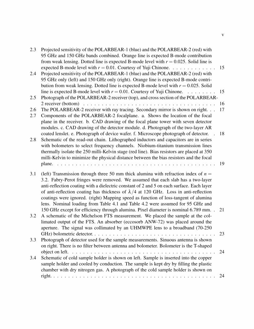
2.3 Projected sensitivity of the POLARBEAR-1 (blue) and the POLARBEAR-2 (red) with95 GHz and 150 GHz bands combined. Orange line is expected B-mode contributionfrom weak lensing. Dotted line is expected B-mode level with r = 0.025. Solid line isexpected B-mode level with r = 0.01. Courtesy of Yuji Chinone. . . . . . . . . . . . . 15
2.4 Projected sensitivity of the POLARBEAR-1 (blue) and the POLARBEAR-2 (red) with95 GHz only (left) and 150 GHz only (right). Orange line is expected B-mode contri-bution from weak lensing. Dotted line is expected B-mode level with r = 0.025. Solidline is expected B-mode level with r = 0.01. Courtesy of Yuji Chinone. . . . . . . . . 15
2.5 Photograph of the POLARBEAR-2 receiver (top), and cross section of the POLARBEAR-2 receiver (bottom) . . . . . . . . . . . . . . . . . . . . . . . . . . . . . . . . . . . . 16
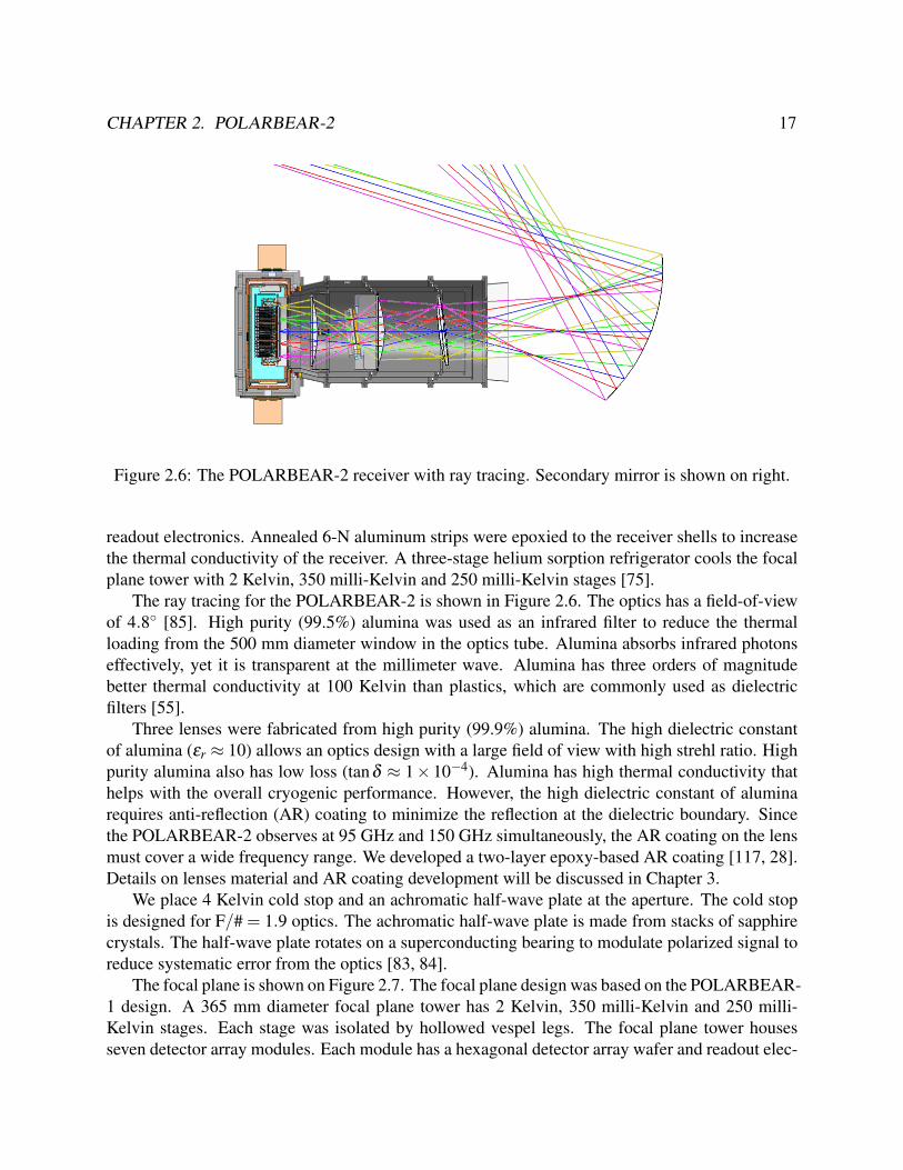
2.6 The POLARBEAR-2 receiver with ray tracing. Secondary mirror is shown on right. . . 172.7 Components of the POLARBEAR-2 focalplane. a. Shows the location of the focal
plane in the receiver. b. CAD drawing of the focal plane tower with seven detectormodules. c. CAD drawing of the detector module. d. Photograph of the two-layer ARcoated lenslet. e. Photograph of device wafer. f. Microscope photograph of detector. . 18
2.8 Schematic of the read-out chain. Lithographed inductors and capacitors are in serieswith bolometers to select frequency channels. Niobium-titanium transmission linesthermally isolate the 250 milli-Kelvin stage (red line). Bias resistors are placed at 350milli-Kelvin to minimize the physical distance between the bias resistors and the focalplane. . . . . . . . . . . . . . . . . . . . . . . . . . . . . . . . . . . . . . . . . . . . 19
3.1 (left) Transmission through three 50 mm thick alumina with refraction index of n =3.2. Fabry-Perot fringes were removed. We assumed that each slab has a two-layeranti-reflection coating with a dielectric constant of 2 and 5 on each surface. Each layerof anti-reflection coating has thickness of λ/4 at 120 GHz. Loss in anti-reflectioncoatings were ignored. (right) Mapping speed as function of loss-tangent of aluminalens. Nominal loading from Table 4.1 and Table 4.2 were assumed for 95 GHz and150 GHz except for efficiency through alumina. Pixel diameter is nominal 6.789 mm. . 21
3.2 A schematic of the Michelson FTS measurement. We placed the sample at the col-limated output of the FTS. An absorber (eccosorb ANW-72) was placed around theaperture. The signal was collimated by an UHMWPE lens to a broadband (70-250GHz) bolometric detector. . . . . . . . . . . . . . . . . . . . . . . . . . . . . . . . . . 23
3.3 Photograph of detector used for the sample measurements. Sinuous antenna is shownon right. There is no filter between antenna and bolometer. Bolometer is the T-shapedobject on left. . . . . . . . . . . . . . . . . . . . . . . . . . . . . . . . . . . . . . . . 24
3.4 Schematic of cold sample holder is shown on left. Sample is inserted into the coppersample holder and cooled by conduction. The sample is kept dry by filling the plasticchamber with dry nitrogen gas. A photograph of the cold sample holder is shown onright. . . . . . . . . . . . . . . . . . . . . . . . . . . . . . . . . . . . . . . . . . . . . 24

vi
3.5 (left) Transmission through 4 mm thick 99.9% purity alumina measuered at room tem-perature. Refraction index was n = 3.20±0.01. (right) Transmission through 40 mmthick 99.9% purity alumina measured at 100 Kelvin. Loss-tangent was tan(δ ) =(0.9±0.2)×10−4. . . . . . . . . . . . . . . . . . . . . . . . . . . . . . . . . . . . . 25
3.6 Schematic for characteristic method calculation. E+n and E−n are incoming and re-
flected electric field at layer n respectively. [49] . . . . . . . . . . . . . . . . . . . . . 263.7 Frequency normalized transmission for AR coating on alumina (εr = 10). Each layer
is λ/4 at center frequency f0. For single layer coating εr = 3.2. For two layer coatings,εr = 2,5. For three layer coatings, εr = 2,4,7 were used. . . . . . . . . . . . . . . . . 27
3.8 Dielectric constants of various epoxy and SrTiO3 mixtures at room temperature as afunction of the percent by weight of the total mixture. . . . . . . . . . . . . . . . . . . 29
3.9 Photograph of two-layer AR coated alumina sample. AR coating is applied on bothside. Sample is 6 mm thick and 50 mm in diameter. Coatings were 354 µm, and 224µm for Stycast 1090 layer and Stycast 2850FT layer respectively . . . . . . . . . . . . 29
3.10 Transmittance spectra of two-layer (top) and three-layer (bottom) AR coated aluminaat 300 Kelvin (solid black) and 140 Kelvin (dashed red), the modeled curve at 300Kelvin (dash-dotted blue), and uncoated alumina (dotted magenta). A widened trans-mittance band can be inferred from the lack of Fabry-Perot fringes. . . . . . . . . . . . 30
3.11 (left) CAD drawing of cross section of a piston and a mold. (right) Photograph ofpiston with a coated lenslet. Photograph of cavity with small drop of epoxy inside.Courtesy of Praween Siritanasak . . . . . . . . . . . . . . . . . . . . . . . . . . . . . 31
3.12 (left)Photograph of lenslet coating for inspection. Curve fitting finds contrast in imageand fits circle with center position and radius as free parameter. (right) Photograph ofmicrometer setup to check thickness of stripped coating directly. Courtesy of PraweenSiritanasak . . . . . . . . . . . . . . . . . . . . . . . . . . . . . . . . . . . . . . . . . 31
4.1 CAD drawing of focal plane planning. Circle represent 365 mm available focal planearea. Hexagon is 120 mm side to side. . . . . . . . . . . . . . . . . . . . . . . . . . . 34
4.2 Number of close packed circular pixels as function of pixel size for 365 mm diameterfocal plane with seven hexagonal wafers. Each hexagonal wafer is 110 mm wide. . . . 35
4.3 Simple model of a cryogenic receiver. Dark blue box represents a cold box with anaperture (Lyot stop). Green hemisphere represents a lenslet of a detector. Circular fancoming out from a lens represents detector beam. Arrows represent optical loadingcontributions from optical elements. . . . . . . . . . . . . . . . . . . . . . . . . . . . 38
4.4 Transmission of atmosphere for 1 mm PWV 60 degrees elevation between 50 GHz and350 GHz. . . . . . . . . . . . . . . . . . . . . . . . . . . . . . . . . . . . . . . . . . 39
4.5 CAD of the simulated 3-D model. 16-cell sinuous antenna was placed under lensletwith differential excitation. Radius of silicon (εr = 11.7) lenslet is R = 2.673 mm.Two layer AR coating was represented by two shells with εr = 2,5, with thickness ofλ/4 at 120 GHz. Silicon cylinder extension has radius of sum of radius of lensletteand thickness of AR coatings. . . . . . . . . . . . . . . . . . . . . . . . . . . . . . . . 41

vii
4.6 Directivity of the beam on E-plane for various L/R ratio for 95 GHz (left) and 150 GHz(right). . . . . . . . . . . . . . . . . . . . . . . . . . . . . . . . . . . . . . . . . . . . 41
4.7 Integrated directivity for 95 GHz (left) and 150 GHz (right). Directivity was integrateddown to the angle defined by F/#. . . . . . . . . . . . . . . . . . . . . . . . . . . . . 42
4.8 Gaussian beam waist size for simulated beam for 95 GHz (left) 150 GHz (right) . . . . 424.9 (left) Spill over efficiency for F/# = 1.9 and waist to pixel diameter ratio of D/w0 =
2.95 . (right) Effect of Lyot temperature to mapping speed. . . . . . . . . . . . . . . . 434.10 Plot of normalized NEPg as function of Tc
Tb. Phonon conduction (n = 3) is assumed.
Plot is normalized to minima of the the curve. . . . . . . . . . . . . . . . . . . . . . . 474.11 Normalized beam calculated from truncated gaussian at radius of 1.25 m. F/# = 1.9,
D = 6.789 mm and waist to pixel diameter ratio of D/w0 = 2.95 were assumed . . . . 514.12 (left) Tc measurement of AlTi bilayer sample with linear fit to transition part of the
curve. Courtesy of Ben Westbrook. (right) Calculated loop gain for RT ES/RN with α
measured from Tc curve. . . . . . . . . . . . . . . . . . . . . . . . . . . . . . . . . . 524.13 Mapping speeds were calculated for various center frequency and fractional band-
width. For parameters that does not change as function of center frequency and frac-tional bandwidth (ex. pixel size) nominal values were used. . . . . . . . . . . . . . . . 54
4.14 Mapping speed as function of pixel diameter. . . . . . . . . . . . . . . . . . . . . . . 544.15 CAD drawing of detector array with circle representing 150 mm diameter wafer. . . . . 564.16 (left) Photograph of sinuous array in POLARBEAR-1 spare invar holder. (right)
POLARBEAR-1 spare lenslet array was used for testing . . . . . . . . . . . . . . . . 57
5.1 Extension length as a function of dielectric constant of lens [35]. . . . . . . . . . . . . 635.2 CAD of a pixel. Sinuous antenna is at the center of the pixel. Four diplexer filters
surround the sinuous antenna. Four optical bolometers surrounds the filters. Darkbolometers and test structures surrounds optical bolometers. Twelve pads at the edgeof circle connects wiring inside of pixel to on-wafer wiring. . . . . . . . . . . . . . . . 63
5.3 Samples of broadband log-periodic planar antennas. From left: bow-tie antenna, log-spiral antenna, log-periodic antenna and sinuous antenna. . . . . . . . . . . . . . . . 64
5.4 Photograph of a sinuous antenna. This sinuous antenna has 11-cell, α = 45, δ =22.5, τ = 1.3 and R1 = 24 µm. . . . . . . . . . . . . . . . . . . . . . . . . . . . . . 65
5.5 Example of complementary structure. Sinuous antenna is self -complementary that slot(white) and metal (colored) region has identical shape. . . . . . . . . . . . . . . . . . 66
5.6 Input impedance of antenna from full 3D simulation. . . . . . . . . . . . . . . . . . . 675.7 Schematic of differential excitation at feed point[33] . . . . . . . . . . . . . . . . . . 675.8 Impedance of niobium microstrip line with 0.5 µm thick silicon oxide (εr = 3.8) as
functoin of strip width. . . . . . . . . . . . . . . . . . . . . . . . . . . . . . . . . . . 685.9 Reflection at antenna feed as function of width of strip for niobium microstrip line with
0.5 µm thick silicon oxide (εr = 3.8) . . . . . . . . . . . . . . . . . . . . . . . . . . . 695.10 Microscope photograph of center of sinuous antenna with cross over (left) and without
(right) . . . . . . . . . . . . . . . . . . . . . . . . . . . . . . . . . . . . . . . . . . . 69

viii
5.11 (left) Sinuous antenna with three different τ value (right) Simulated polarization wob-ble angle and maximum cross-pol level for different τ [33]. . . . . . . . . . . . . . . . 71
5.12 Comparison of measured beam shape for 11-cell sinuous antenna (top row) and 16-cellsinuous antenna (bottom row). Left column shows 95 GHz beam and right columnshown 150 GHz beam. Ellipticity for 95 GHz and 150 GHz 11-cell beam was 4.0%and 1.0% respectively. Ellipticity for 95 GHz and 150 GHz 17-cell beam was 1.2%and 1.5% respectively. . . . . . . . . . . . . . . . . . . . . . . . . . . . . . . . . . . 72
5.13 3-D EM simulation result for 80 GHz beam with 11-cell (left) and 17-cell (right) sinu-ous antenna. Current density is shown on top row. For 11-cell antenna, edge of sinuousantenna shows sign of left over current. . . . . . . . . . . . . . . . . . . . . . . . . . . 73
5.14 (left) Ellipticity as function of frequency and number of cells. (right) Polarizationwobble as function of number of cells . . . . . . . . . . . . . . . . . . . . . . . . . . 73
5.15 Band-averaged beam from 75 GHz to 105 GHz. From left, 11-cell, 14-cell and 17-cell sinuous antenna’s beam is shown. Beam had 5.05%, 3.53% and 1.45% ellipticityrespectively. . . . . . . . . . . . . . . . . . . . . . . . . . . . . . . . . . . . . . . . . 74
5.16 Input impedance of sinuous antenna in vacuum as function of frequency. 11-Cell an-tenna’s impedance start to deviate from expected 267 Ω of self-complementary antennaat low frequency. . . . . . . . . . . . . . . . . . . . . . . . . . . . . . . . . . . . . . 74
5.17 3-D normalized beam of sinuous antenna in vacuum. 11-cell sinuous antenna’s beamis shown on top, and 17-cell sinuous antenna’s beam is shown on bottom. 11-cellantenna has interesting fan like shape at low frequency, where as 17-cell antenna hasexpected beam shape. . . . . . . . . . . . . . . . . . . . . . . . . . . . . . . . . . . . 75
5.18 (left) Comparison of simulated wobble angle and measurement of the sinuous antennaat 8 GHz to 25 GHz. Discrepancy between simulation and measurement comes fromexlusion of 10 mil subtrate layer (εr = 10.2) in simulation [33]. (right) 3-D EM simu-lation result between 70 GHz to 170 GHz. . . . . . . . . . . . . . . . . . . . . . . . . 76
5.19 Two different sense of the sinuous antenna . . . . . . . . . . . . . . . . . . . . . . . . 765.20 (Left) Q pixel of slot dipole antenna (Right) U pixel of slot dipole antenna . . . . . . . 775.21 Polarized signal (green) coming in at angle θ respect to detector coordinate. Two
senses and Q/U pixel combinations are shown. . . . . . . . . . . . . . . . . . . . . . . 785.22 Circuit diagram for filter design. a. Low-pass prototype design. b. Band-pass design.
c. Circuit diagram for a stub. d. Band-pass design with impedance inverter. e. Lumpedfilter design with T-capacitor network. f. Lumped filter design with π-capacitor network 83
5.23 Stub filter design for 150 GHz . . . . . . . . . . . . . . . . . . . . . . . . . . . . . . 865.24 Three lumped filter design in chronogical order. (top) Lumped filter design with co-
planar inductor design with via. (middle) Lumped filter design with microstrip induc-tor design without via. (bottom) Lumped filter design with co-planar inductor designwithout via . . . . . . . . . . . . . . . . . . . . . . . . . . . . . . . . . . . . . . . . 87
5.25 Lumped filter design for 150 GHz. Zoomed in CAD for capacitor part shows possibleparasitic capacitance . . . . . . . . . . . . . . . . . . . . . . . . . . . . . . . . . . . 87
5.26 Response of lumped diplexer. Atmospheric transmission line is added to show atmo-spheric window. . . . . . . . . . . . . . . . . . . . . . . . . . . . . . . . . . . . . . . 88

ix
5.27 Comparison of original design and design with top layer shifted by 0.5 µm in X-Ydirection. . . . . . . . . . . . . . . . . . . . . . . . . . . . . . . . . . . . . . . . . . 89
5.28 Simulation of filter design with varying coplanar strip width. Band shape could be im-proved by modifying capacitance values at same time. Simulation shows band locationcan be modified far enough with just modifying top layer. . . . . . . . . . . . . . . . . 89
5.29 Comparison of shift in band location due to pixel location on wafer for stub filter (left)and lumped filter (right) . . . . . . . . . . . . . . . . . . . . . . . . . . . . . . . . . . 90
5.30 Comparison of size difference for 150 GHz filter. Lumped filter is shown on top andstub filter is shown on bottom. . . . . . . . . . . . . . . . . . . . . . . . . . . . . . . 91
5.31 Microscope photograph of crossover (left). Simulated responce is shown on right.Reflection was suppressed under -20 dB across required bandwidth. . . . . . . . . . . 92
5.32 Microscope photograph of bolometer island (left) and bolometer (right). Dark back-ground around bolometer is due to cavity formed by XeF2 silicon etching. . . . . . . . 94
5.33 Expected detector efficiency assuming loss-tangent between 1× 10⁻³ and 7× 10⁻³.Black line in center assumes 4×10⁻³ . . . . . . . . . . . . . . . . . . . . . . . . . . 95
5.34 (left) Microscope photograph of bondpad. Vertical metal object is a wirebonding tip.(right) Microscope photograph of wiring layer. Wiring layer is connected to pixelwiring at two white pads in center of the photograph. . . . . . . . . . . . . . . . . . . 96
5.35 (left) Photograph of wafer in process. Detector array uses 150 mm wafer fully. (right)Photograph of detector wafer. . . . . . . . . . . . . . . . . . . . . . . . . . . . . . . . 96
5.36 Microscope photograph of detector pixel. Sinuous antenna is on top. Transmissionline snakes out of the sinuous antenna. Broadband signal is split into frequency bandsat diplexing filter. Transmission lines crossover prior to detection at bolometer. . . . . 97
5.37 3-D microscope photograph of various parts of detector. 3-D microscope photographallows us to check step coverage and alignment in new way. . . . . . . . . . . . . . . . 98
5.38 Step by step cross-section of fabrication. Step number corresponds to step ID in Table 5.3 995.39 Microscope photograph of half released bolometer (left) and fully released bolometer
(right). Ground plane was removed from bolometer such that silicon underneath isvisible. Half-released bolometer shown unetched silicon under low stress nitride. . . . 103
5.40 (left) SEM photograph of seating wafer cross section. (right) Photograph of partiallypopulated lenslet array. Cortesy of Praween Siritanasak . . . . . . . . . . . . . . . . . 104
5.41 (left) Schematic drawing of alignment process. Device wafer and lenslet array wafer ismounted in an invar holder. Then alignment marks etched in both wafers were alignedwith IR microscope. (right) Photograph of two alignment marks being aligned. Fuzzycross mark is from device wafer. Sharper stub is from lenslette wafer. . . . . . . . . . 105
5.42 Photograph of detector wafer mounted in invar holder. Proto-type readout flexiblecable is also attached. Backing plate is shown on right with ANW-72 absorber attached. 105
5.43 Schematic drawing of absorber test setup. . . . . . . . . . . . . . . . . . . . . . . . . 1065.44 Beam from backshort testing. Beam with carbon loaded stycast as absorber material is
shown in left. Beam with ANW-72 as absorber is shown in right. . . . . . . . . . . . . 1075.45 Photograph of wafer with interdigitated capacitor and inductors. Zoomed in micro-
scope photograph is shown on right . . . . . . . . . . . . . . . . . . . . . . . . . . . . 108

x
5.46 (left) Circuit diagram for ESR testing (right) Result from ESR testing is shown onright. Loss from interdigitated capacitor fabricated on high resistivity silicon is lower. . 108
5.47 Photograph of POLARBEAR-2 detector module assembly with proto-type lenslet ar-rays and read-out board from the SPT-pol experiment . . . . . . . . . . . . . . . . . . 109
5.48 Photograph of plexiglass shipping container (left). Shipping container inside foamedcase (right). . . . . . . . . . . . . . . . . . . . . . . . . . . . . . . . . . . . . . . . . 110
6.1 Cross section of 8 inch IR Labs dewar. Milli-Kelvin stage is buffered by liquid nitro-gen and liquid helium stage. 250 milli-Kelvin base temperature is probided by 3Headsorption fridge. Dewar was modified with Zotefoam window and thermal filters topass millimeter wave into the dewar. . . . . . . . . . . . . . . . . . . . . . . . . . . . 112
6.2 Circuit diagram for readout electronics. Colors separate circuit at different temperatures.1136.3 Photograph of large lens test setup. How detector pixel is mounted is shon on bottom
right. . . . . . . . . . . . . . . . . . . . . . . . . . . . . . . . . . . . . . . . . . . . . 1146.4 Photograph of fabricated detector wafers. We fabricated sinuous array in POLARBEAR-
2 array size, POLARBEAR-1 array size and 2 pixel chip. . . . . . . . . . . . . . . . . 1146.5 Photograph of POLARBEAR-1 size array test setup . . . . . . . . . . . . . . . . . . . 1156.6 Photograph of POLARBEAR-1 size sinuous array mounted on invar holder. ANW-72
backabsorber terminates backlobe of antenna. Setup required long wirebond as shownin bottom right of the picture. . . . . . . . . . . . . . . . . . . . . . . . . . . . . . . . 116
6.7 Photograph of small lens setup with 2 pixel detector array. Zoom in photo of custominvar holder is shown in bottom right. . . . . . . . . . . . . . . . . . . . . . . . . . . 117
6.8 Cross section of POLARBEAR-2 optical test cryostat. Cooling power is provided bypulse-tube cooler. Milli-Kelvin temperature is provided by three-stage helium cooler.Dewar was modified from its original configuration used by APEX-SZ experiment byadding optical window and shells above plane of RF-shield. . . . . . . . . . . . . . . . 118
6.9 a) Photograph of POLARBEAR-2 optical test cryostat. b) Zoom in photograph of de-tector array mounted on milli-Kelvin stage c) Detector array mounted on milli-Kelvinstage with RF-shield installed. . . . . . . . . . . . . . . . . . . . . . . . . . . . . . . 119
6.10 Circuit diagram of dfMUX readout system [31] . . . . . . . . . . . . . . . . . . . . . 1206.11 Photograph of the FTS setup. Output of FTS is reflected upwards by 45 degree mirror.
Then beam was focused into dewar. When making band measurement of detector,sample holder shown on bottom right is removed. . . . . . . . . . . . . . . . . . . . . 120
6.12 Photograph of the beam map measurement. Temperature modulated source (upperright) is mounted on X-Y stage. Polarization measurement was made at boresight byrotating wiregrid polarizer on top of temperature modulated source. CAD drawing ofpolarizer setup is shown on bottom right. . . . . . . . . . . . . . . . . . . . . . . . . 121
6.13 Spectrum of a distributed diplexer (left) and a distributed triplexer (right). A and Brefers to two orthogonal linear polarization channels. Peaks are normalized to themeasured optical efficiency. See Table 6.2 for details. . . . . . . . . . . . . . . . . . . 123
xi
6.14 Spectrum of a lumped diplexer with 11-cell sinuous antenna (left) and spectrum of alumped diplexer with 16-cell (right). A and B refers to two orthogonal linear polariza-tion channels. Peaks are normalized to measured optical efficiency. See Table 6.2 fordetails. . . . . . . . . . . . . . . . . . . . . . . . . . . . . . . . . . . . . . . . . . . . 123
6.15 Spectrum of a lumped diplexer with 16-cell sinuous antenna under small lenslet. Datawere taken from pixel #45 and #47 shown on right. Data were peak normalized andsimulation result was overlayed. . . . . . . . . . . . . . . . . . . . . . . . . . . . . . 124
6.16 Beammap result from distributed diplexer. 95 GHz beam is shown on left and 150 GHzbeam is shown on right. See Figure 6.13 for exact band location. See Table 6.2 fordetails. . . . . . . . . . . . . . . . . . . . . . . . . . . . . . . . . . . . . . . . . . . . 125
6.17 Beammap result from lumped diplexer. 95 GHz beam is shown on left and 150 GHzbeam is shown on right. See Figure 6.14 for exact band location. See Table 6.2 fordetails. . . . . . . . . . . . . . . . . . . . . . . . . . . . . . . . . . . . . . . . . . . . 126
6.18 Beammap result from distributed diplexer. 95 GHz beam is shown on left and 150 GHzbeam is shown on right. See Figure 6.13 for exact band location. See Table 6.2 fordetails. . . . . . . . . . . . . . . . . . . . . . . . . . . . . . . . . . . . . . . . . . . . 127
6.19 Beammap result from lumped diplexer under 14 mm lens (top) and 6.35 mm lens(bottom). 95 GHz beam is shown on left and 150 GHz beam is shown on right. SeeFigure 6.14 for exact band location. See Table 6.2 for details. . . . . . . . . . . . . . . 128
6.20 Beammap result from lumped diplexer under 6.35 mm lens. 2-D gaussian was fit. Twolines in beam represent axis of 2-D gaussian. Slice were taken along the axis, and fiton gaussain in the plane of axis is plotted. 95 GHz beam is shown on left and 150 GHzbeam is shown on right. See Figure 6.14 for exact band location. See Table 6.2 fordetails. . . . . . . . . . . . . . . . . . . . . . . . . . . . . . . . . . . . . . . . . . . . 129
6.21 Responses of the distributed diplexer (left) and distributed triplexer (right) to a linearlypolarized source as a function of relative angle between antenna and the polarizer.Plots were peak normalized prior to fitting by sum of a sine function and a constant.Cross-pol for each channels are summarized in Table 6.2. . . . . . . . . . . . . . . . . 129
6.22 Responses of the lumped diplexer with 11-cell sinuous antenna (left) and lumpeddiplexer with 16-cell sinuous antenna (right) to a linearly polarized source as a func-tion of relative angle between antenna and the polarizer. Plots were peak normalizedprior to fitting by sum of a sine function and a constant. Cross-pol for each channelsare summarized in Table 6.2. . . . . . . . . . . . . . . . . . . . . . . . . . . . . . . . 130
6.23 (left) I-V curve while detector is receiving optical locating from 300 Kelvin load and77 Kelvin load. (right) I-V curve and R-P curve showing that detector biased down to0.65RN . . . . . . . . . . . . . . . . . . . . . . . . . . . . . . . . . . . . . . . . . . . 130
6.24 Preliminary spectrum data from POLARBEAR-2 optical cryostat. Band is placed be-tween atmospheric windows. . . . . . . . . . . . . . . . . . . . . . . . . . . . . . . . 131
6.25 Preliminary beam map (left) and polarization data (right) from POLARBEAR-2 opti-cal cryostat. Lenslet quality and cross-talk needs to improve to make accurate mea-surement on these two parametes in future. . . . . . . . . . . . . . . . . . . . . . . . . 131

xii
7.1 CAD drawing of proposed POLARBEAR-2’s focal plane (left) SPT-3G’s focal plane(center) LiteBIRD’s focal plane (right) . . . . . . . . . . . . . . . . . . . . . . . . . . 133
7.2 Prototype lumped triplexer design is shown on left. Simulated result is shown on rightwith 1 mm PWV atmospheric transmission. . . . . . . . . . . . . . . . . . . . . . . . 135
7.3 Sinuous antenna with oscillating arm. Oscillation slows wave speed on antenna. Thisallows smaller physical size of antenna [82]. . . . . . . . . . . . . . . . . . . . . . . . 136
7.4 Suggestion for rerouting of transmission line on sinuous antenna. Current design fol-lows sinuous antenna’s curve (dark blue). By cutting corners as shown in light green,over all length of transmission line becomes shorter, and radius of curvature increasesthat would suppress reflection at corners. . . . . . . . . . . . . . . . . . . . . . . . . . 137
7.5 CAD drawing of detector pixel with a photograph of a dark bolometer. The darkbolometer was placed outside of wirebonding pads. Bolometer’s slot was orientedparallel to one polarization of the antenna. . . . . . . . . . . . . . . . . . . . . . . . . 138
7.6 (left) Response of dark bolometer to rotating wiregrid infront of modulating thermalsource. Response was normalized. Dark bolometer’s beam was partially polarized,and its polarization was perpendicular to its slot. (right) beam map of dark bolome-ter. Beam was elongated along slot of bolometer, and beam was steered towards darkbolometer. . . . . . . . . . . . . . . . . . . . . . . . . . . . . . . . . . . . . . . . . . 138
7.7 Spectrum measurement of an optical pixel to higher freqency. We suspect rising spec-trum starting around 250 GHz is due to direct stimulation. . . . . . . . . . . . . . . . . 139
7.8 Response of optical and dark bolometer to temperature modulated source. B09Sq3Ch3is a dark bolometer. Other channels are optical. Dark bolometer responds to opticalsignal without filter (left). Dark bolometer still responds with 300 GHz low pass filterbetween source and detector (center). With 168 GHz low pass filter in place, the darkbolometer does not respond to a signal (right). Optical bolomters are still seeing signal.Slight decrease in optical signal with 168 GHz is because it overlaps with designedband slightly. Courtesy of Z. Kermish. . . . . . . . . . . . . . . . . . . . . . . . . . . 139
7.9 (left) EM simulation of slot curved in infinite perfect conductor in shape of bolometer.Current density is shown. High density of current flows at edge of bolometer island.Schematic drawing of bolometer island is shown on right. Lossy metals such as goldand aluminum-titanium could pick up these currents via inductive coupling. . . . . . . 140
7.10 Schematic drawing of grooved AR coating (bottom left). Photograph of alumina sam-ple coated with grooved stycast 2850FT. Groove was made with wafer dicing saw.Microscope photograph of groove is shown on bottom right. . . . . . . . . . . . . . . 141
7.11 Dimples drilled in alumina with laser pulse [92] . . . . . . . . . . . . . . . . . . . . . 1427.12 50 mm alumina disk thermal spray coated with 250 µm thick mullite . . . . . . . . . . 142

xiii
List of Tables
1.1 Current limit on selected parameters [115, 2, 1]. . . . . . . . . . . . . . . . . . . . . . 111.2 Lists of recent CMB polarization experiments [90] . . . . . . . . . . . . . . . . . . . 11
3.1 Transmission through three 50 mm alumina lenses for 95 GHz band and 150 GHzband. We assume each slab has two-layer anti-reflection coating with dielectric con-stant of 2 and 5 on both surface. Each layer of anti-reflection coating has thickness ofλ/4 at 120 GHz. Loss in anti-reflection coatings were ignored. . . . . . . . . . . . . . 22
3.2 Summary of results from alumina measurements. . . . . . . . . . . . . . . . . . . . . 25
4.1 List of optical elements for fcenter = 94.3 GHz and FracBW = 30.6%. Loss through thefield lens, aperture lens and collimating lens assume tanδ = 1× 10⁻⁴ dielectric loss.Microstrip loss assumes tanδ = 2×10⁻³ dielectric loss . . . . . . . . . . . . . . . . . 36
4.2 List of optical elements for fcenter = 147.8 GHz and FracBW = 26.0%. Loss throughfield lens, aperture lens and collimating lens assume tanδ = 1× 10⁻⁴ dielectric loss.Microstrip loss assumes tanδ = 2×10⁻³ dielectric loss . . . . . . . . . . . . . . . . . 37
4.3 Detector parameters . . . . . . . . . . . . . . . . . . . . . . . . . . . . . . . . . . . . 584.4 Readout parameters . . . . . . . . . . . . . . . . . . . . . . . . . . . . . . . . . . . . 594.5 Focal plane parameters . . . . . . . . . . . . . . . . . . . . . . . . . . . . . . . . . . 594.6 Lists of observation efficiency. Conservative estimates were given to each entry. Cour-
tesy of Yuji Chinone. . . . . . . . . . . . . . . . . . . . . . . . . . . . . . . . . . . . 594.7 Summary of POLARBEAR-2 Sensitivity . . . . . . . . . . . . . . . . . . . . . . . . 60
5.1 Specific Heat at 0.5 Kelvin for materials used on bolometer island [77, 124, 98, 103,14, 57, 132] . . . . . . . . . . . . . . . . . . . . . . . . . . . . . . . . . . . . . . . . 93
5.2 Bolometer parameters . . . . . . . . . . . . . . . . . . . . . . . . . . . . . . . . . . . 945.3 Summary of fabrication steps. Step ID corresponds to step number shown in Figure 5.38.1005.4 Reflection of absorbers at 150 GHz [120]. . . . . . . . . . . . . . . . . . . . . . . . . 106
6.1 Summary of tested detectors . . . . . . . . . . . . . . . . . . . . . . . . . . . . . . . 1226.2 Summary from one of the polarizations of each diplexer and triplexer. ν0 is the center
frequency of the band and ∆ν is integrated bandwidth. Cross-pol values are upper limitvalue as we expect leakage from wire-grid . . . . . . . . . . . . . . . . . . . . . . . . 127

xiv
7.1 Lists of proposed experiment with sinuous antenna multichroic detector array . . . . . 134
xv
Acknowledgments
This is the most difficult section in the thesis. I met so many people that had positive influence onme. I cannot possibly mention everybody here. I apologize in advance for people I was not able toinclude here.
I would like to thank my advisor Adrian Lee. His support and freedom he gave me made itpossible for me to be creative. He is unique in the field that he trains students to learn detectorfabrication techniques. Such skill is highly desired in our field, and also beyond our field. I wouldlike to thank Paul Richards for many advices he gave me. His advice was helped me to succeed inresearch, but it also helped me to become better scientist overall. Bill Holzapfel always had usefulsuggestions. His advice turned troubling dewar into the cold dewar. When Billy and I were stuckon sealing method for 3He adsorption fridge, Bill gave us an advice that allow us to seal it on thefirst try.
I was surrounded by great graduate students. Roger O’Brient dedicated so much of his busyschedule at the end of his graduate career to train me. He was a great mentor that in half yearhe trained me in so many things that I needed to survive. He kept giving me advices and ideaseven after his graduation. I inherited his work and pushed on, so much of this thesis stems fromhis ideas and his work. Mike Myers gave suggestions that steered research into right direction atcritical points. Kam Arnold taught me art of making detector array. Many of detector array designstems from POLARBEAR-1 detector array that he designed and fabricated. In private life. hisadvice on where to propose in Hawaii island definitely helped. Ziggy Kermish always had answerwhen we asked him how we should go about designing the POLARBEAR-2 receiver. Erin Quealyand I worked together on broadband anti-reflection coating problem. I learned importance ofpaying attention to details from working with her. Bryan Steinbach’s sharp questions pushed me tobecome more quantitative scientist. Ben Westbrook was great lab-buddy and fab-buddy. We sharedmany dewar runs together. Adnan Ghribi gave me many useful suggestion when superconductordid not behave the way I wanted. Recently new talents joined out group. Ari Cukierman and ParkerFegrelius will play big role in making the POLARBEAR-2 happen. I was lucky to have talentedundergraduate to work with. Darin Rosen and I worked together on broadband anti-reflectioncoating. It was his idea of mixing different types of epoxy that made the broadband antireflectionto work. It was fun to work with William Walker on 3He adsorption fridge project. We are aboutto fill the fridge with 3He. I cannot wait to see how it would work.
Microwave engineering work was done with collaborative effort with UCB physics department,UCB astronomy department and UCSD electrical and computer enginering department. GregEngargiola gave me an idea to remove via at center of antenna. Gabriel Rebeiz provided helpfulrule of thumbs that helped to come up with initial design. Jen Edwards did careful study of sinuousantenna with silicon lens. I borrowed a lot of antenna behavior from her work. Her successful workon sinuous antenna gave me confidence to push on to make sinuous antenna work at millimeterwavelength.
Many people from UCSD contributed to the work. It was helpful to have Brian Keating’scomments on papers and proceedings. Although I almost drowned, surfing with him at UCSD wasfun. I would like to thank Praween Siritanasak for his work on the POLARBEAR-2 lenslet. His
xvi
work was crucial since detector is only complete with the lenslet. He also helped me with detectorsimulation work. Stephanie Moyerman helped to fabricate lenslet seating wafer. Darcy Barronshelped us put together POLARBEAR-2 optical test dewar. It was fun deploying to Chile with NateStebor and Dave Boettger. Without Dave, I could not meet quinoa.
I would like to thank Masashi Hazumi to let me visit KEK often and participate many pro-fessional events in Japan. It was very helpful to be able to exchange information face to face. Ienjoyed exchanging ideas freely with Takayuki Tomaru. I learned many hands on techniques fromhim. I also enjoyed working with Takahiro Okamura until late at night at KEK. Suguru Takadataught me tricks in cryogenics. Tomotake Matsumura and I worked together on the material devel-opment. Tomo figured out how to improve the Fourier transform spectrometer setup for materialdevelopment. Masaya Hasegawa took me out every night when I visited KEK. Yuji Chinone taughtme most of cosmology I know. Without him I could not pass the qualification exam. Whenever Ihad question about polarization, Haruki Nishino was always there to give me an advice. Workinguntil late at night with Hideki Morii was always enjoyable. I miss going to gym with him. Kaori’smeasurement on interdigitated capacitor was crucial for its R&D. Yuki Inoue’s accurate measure-ment on material and anti-reflection coating gave confidence in our design. It was fun to workwith Yuta Kaneko to create DC SQUID readout from scratch to test bolometers. I learned so muchabout SQUID through that process.
I borrowed so much of mapping speed calculation from Nils Halverson’s memo. His commentsduring mapping speed discussion helped me to develop the code that I used extensively to optimizethe focal plane. Readout parameter would not converged without input from Matt Dobbs. Colinmade stay at Chile enjoyable. I cannot wait to see the dewar at Dalhousie taking data with thePOLARBEAR-2 wafer. It was critical to have talented machinists in our building to make rapidprogress that we made. Machinists at physics machine shop did not just machined beautiful partsfor us. They were great advisors that taught us how design should be done. Pete Thussen especiallytaught me many machining related topics that were critical to designs I made. Xiaofan Menghelped us greatly during fabrication. Xiaofan kept the machine in working condition. He helpedme diagnose odd things I see during fabrication. Exchanging ideas on absorption loss in alumina,anti-reflection coating and simulation method with Tom Nitta was helpful.
I would like to thank YuryKolomensky to give me advices and much needed help at early stageof my graduate student career. Without him I would not be where I am today.
We acknowledge support from the NASA, NASA grant NNG06GJ08G. Detectors were fabri-cated at Berkeley nanofabrication laboratory.
1
Chapter 1
Cosmic Microwave Background
1.1 IntroductionObservations of distant luminous objects showed that the Universe is expanding [52]. Thus, at theearly Universe, we expect the scale of the Universe to be smaller. In the 1940s, Gamow, Alpherand Herman [39, 9] formulated the Big-Band model. In the hot Big-Bang model, the Universe wasonce extremely hot and dense. Hot plasma filled the universe. Photons were tightly coupled toionized electrons and protons through scattering in the early Universe. As the Universe expanded,the average temperature of the Universe dropped. When the Universe was 380,000 years old,the scattering rate between photons, electrons and protons fell below the expansion rate of theUniverse and the photon decoupled from the ionized electrons and protons. At this moment, theCosmic Microwave Background (CMB) was created. Since then, photons have streamed freelythrough the Universe - except for the brief period of time around z = 10 ∼ 6 when the first starsformed - to reionize neutral hydrogen atoms. Reionized hydrogen atoms and photons interactedfor the last time. Studying CMB is a great way to understand the evolution of the Universe becauseit was generated at the very early Universe where perturbations were still linear. It also acts aswell-understood back light source with known black body spectrum. This allowed the detection ofhigh z galaxy through the SunyaevZel’dovich effect. The CMB red-shifted with the expansion ofthe Universe. Today, the CMB has a wavelength of a few millimeters; putting the CMB experimentin a unique field of its own - between radio and infrared astronomy.
Since its discovery in 1965, CMB observations have given us a wealth of information aboutthe Universe [30, 97]. The Far-Infrared Absolute Spectrophotometer (FIRAS) measured the CMBspectrum and found that the CMB has a 2.73 Kelvin black body spectrum [80]. The black bodyspectrum of the CMB is one of the pillars of the hot Big Bang model. Relative temperature mea-surements of the CMB between different parts of the sky showed that the CMB has an anisotropyof the order 10−5 Kelvin. It was first detected by the Differential Microwave Radiometer (DMR)aboarded on the Cosmic Background Explorer satellite (COBE) [114]. Many ground experiments,balloon experiments and satellite experiments have mapped the temperature anisotropy with in-creasing sensitivity and angular resolution. Recently, a full-sky map was published by the Planck
CHAPTER 1. COSMIC MICROWAVE BACKGROUND 2
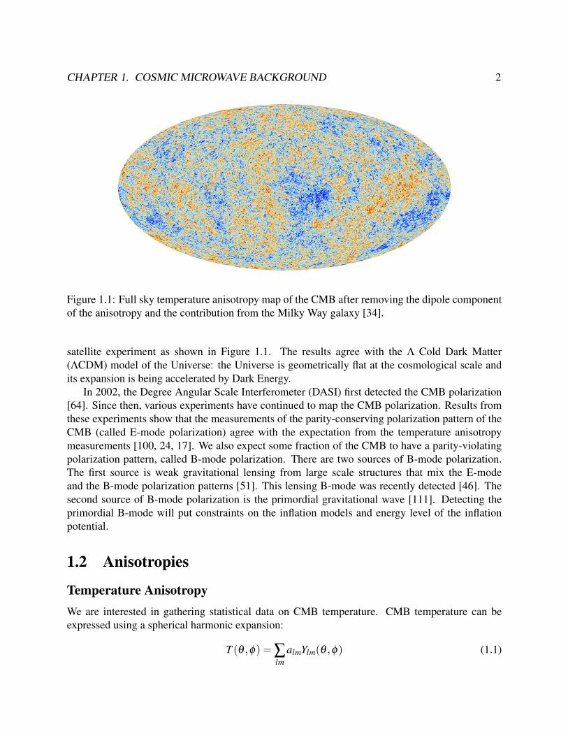
Figure 1.1: Full sky temperature anisotropy map of the CMB after removing the dipole componentof the anisotropy and the contribution from the Milky Way galaxy [34].
satellite experiment as shown in Figure 1.1. The results agree with the Λ Cold Dark Matter(ΛCDM) model of the Universe: the Universe is geometrically flat at the cosmological scale andits expansion is being accelerated by Dark Energy.
In 2002, the Degree Angular Scale Interferometer (DASI) first detected the CMB polarization[64]. Since then, various experiments have continued to map the CMB polarization. Results fromthese experiments show that the measurements of the parity-conserving polarization pattern of theCMB (called E-mode polarization) agree with the expectation from the temperature anisotropymeasurements [100, 24, 17]. We also expect some fraction of the CMB to have a parity-violatingpolarization pattern, called B-mode polarization. There are two sources of B-mode polarization.The first source is weak gravitational lensing from large scale structures that mix the E-modeand the B-mode polarization patterns [51]. This lensing B-mode was recently detected [46]. Thesecond source of B-mode polarization is the primordial gravitational wave [111]. Detecting theprimordial B-mode will put constraints on the inflation models and energy level of the inflationpotential.
1.2 Anisotropies
Temperature AnisotropyWe are interested in gathering statistical data on CMB temperature. CMB temperature can beexpressed using a spherical harmonic expansion:
T (θ ,φ) = ∑lm
almYlm(θ ,φ) (1.1)
CHAPTER 1. COSMIC MICROWAVE BACKGROUND 3
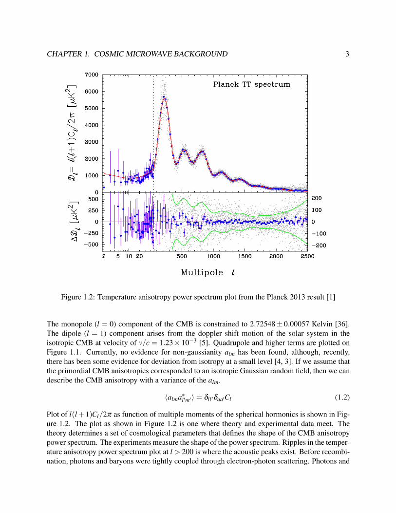
Figure 1.2: Temperature anisotropy power spectrum plot from the Planck 2013 result [1]
The monopole (l = 0) component of the CMB is constrained to 2.72548± 0.00057 Kelvin [36].The dipole (l = 1) component arises from the doppler shift motion of the solar system in theisotropic CMB at velocity of v/c = 1.23× 10⁻³ [5]. Quadrupole and higher terms are plotted onFigure 1.1. Currently, no evidence for non-gaussianity alm has been found, although, recently,there has been some evidence for deviation from isotropy at a small level [4, 3]. If we assume thatthe primordial CMB anisotropies corresponded to an isotropic Gaussian random field, then we candescribe the CMB anisotropy with a variance of the alm.
〈alma∗l′m′〉= δll′δaa′Cl (1.2)
Plot of l(l+1)Cl/2π as function of multiple moments of the spherical hormonics is shown in Fig-ure 1.2. The plot as shown in Figure 1.2 is one where theory and experimental data meet. Thetheory determines a set of cosmological parameters that defines the shape of the CMB anisotropypower spectrum. The experiments measure the shape of the power spectrum. Ripples in the temper-ature anisotropy power spectrum plot at l > 200 is where the acoustic peaks exist. Before recombi-nation, photons and baryons were tightly coupled through electron-photon scattering. Photons and
CHAPTER 1. COSMIC MICROWAVE BACKGROUND 4
baryons were acting as a single fluid. The photon-baryon fluid underwent a series of compressionand expansion under the influence of gravitational potential wells that were setup by dark matter.Since the anisotropy plot shows variance, the peaks represent the size of potential wells that thephoton-baryon fluid is either fully compressed or fully expanded. The troughs represent the sizeof potential wells that the photon-baryon fluids rebounded to the neutral position. These peaksand troughs are dampened at the smaller angular scale. A finite coupling strength between thephotons and baryons allowed the photons to perform a random walk through the fluid to homog-enize the temperature anisotropy at the smaller scale. On the larger angular scale, we do not seeacoustic oscillations since these modes were too large to enter the horizon prior to recombination.The Sach-Wolfe plateaus on a large angular scale, see effect of evolving potential well throughintegrated Sach-Wolfe effect.
InflationThe monopole component of the CMB temperature suggests that points that appears to be notcausally connected share the same temperature. Temperature anisotropy measurements suggestthat the universe is geometrically flat and the perturbation is gaussian. Inflation theory unites thesetwo findings by proposing that the Universe underwent an accelerated expansion period when theUniverse was a fraction of a second old. Superluminal expansion grows the causally connectedpart of the sky beyond the observable universe. Inflation reduces the geometrical curvature smallenough to prevent the Universe from collapsing. Inflation also provides a natural mechanism forthe initial gaussian perturbations for potential wells to form.
We can derive the acceleration equation from time-time and space-space components of thezeroth-order Einstein equation,
aa=−4
3πG(ρ +3p) (1.3)
where a is a scale factor of the Universe. ρ and p represent the energy density and pressure ofthe fields, respectively. The dot represents the derivative against conformal time. Accelerating theuniverse satifies p < −ρ/3. A field that is dominating the Universe during inflation must havenegative pressure. The simple inflation model proposes a single scalar field φ . We can derive theenergy density and pressure of this field from the energy-memtum tensor:
ρ =12
(dφ
dt
)2
+V (φ)
p =12
(dφ
dt
)2
−V (φ) (1.4)
where V (φ) is the potential for the field. A field configuration with negative pressure is one withmore potential energy than kinetic energy. Potential energy is described by two parameters ε(φ)
CHAPTER 1. COSMIC MICROWAVE BACKGROUND 5
and η(φ) which describes the slope and curvature of the potential energy, respectively.
ε(φ) =m2
PL16π
(V ′
V
)η(φ) =
m2PL
8π
(V ′′
V
)(1.5)
where mPL is Planck mass, and prime is the derivative with respect to φ . The amount of expansion,N e-foldings, and potential parameter ε are related by
N ≈ 2√
π
mPL
∫φ f
φi
1√ε(φ)
dφ (1.6)
The N = 64 expansion is required to meet CMB’s observed conditions - homogeneous temperatureand flatness. This requires a small ε , a potential with small slope.
Gravitational WaveInflation-generated perturbations in the scalar part of the metric acts as seeds for potential wells.Inflation also generated gravity waves, tensor fluctuations in the metric. The decomposition theo-rem states that the scalar, vector and tensor parts of the metric perturbations did not couple. Scalarperturbations of the metric coupled with energy density fluctuations. The combined evolution wascomplicated with many degenerate parameters. Since tensor perturbations did not couple to thescalar mode, induced fluctuations in the CMB from tensor mode gives clean detection of signatureof inflation. During inflation, the Universe was filled with an inflationary scalar field and the met-ric. This field fluctuates quantum mechanically, and non-zero variance in this fluctuation evolvesas inflation progresses. Tensor perturbations in the metric can be written with h× and h+ definedas:
gi j = a2
−1 0 0 00 1+h+ h× 00 h× 1−h+ 00 0 0 1
(1.7)
Tensor perturbations evolves as
h+2aa
h+ k2h = 0 (1.8)
where k is a wavevector for perturbation. Defining h transforms this equation. The equationbecomes identical to that of a simple harmonics oscillator (SHO)
¨h+(
k2− aa
)h = 0 (1.9)
Since the average quantum fluctuation is 0, we are interested in the variance of the fluctuation.Thevariance of a quantized SHO can be calculated as
〈 ˆh(~k)† ˆh(~k)〉= (2π)3Phδ3(~k−~k′) (1.10)

CHAPTER 1. COSMIC MICROWAVE BACKGROUND 6
where ˆh(~k) is the quantum operator for the oscillator and Ph is the power spectrum of the primor-dial perturbation to the metric. Ph can be solved by solving for a/a during inflation. The powerspectrum is calculated to be
Ph =8π
k3H2
M2PL
∝ knT−3 (1.11)
Where H is a Hubble rate at the time when the mode of interest leaves the horizon due to inflationexpansion. The Hubble rate is close to constant during inflation because of the small slope ofscalar potential. Since potential energy is bulk energy during the inflationary era, measuring Hwould be equivalent to determining the potential during inflation. Tensor spectral index is zerofor scale invariant (Harrison-Zeldovich) power spectrum, but slow-roll inflationary model predictssome slope in potential define by ε , nT =−2ε .
Scalar perturbations of the metric evolved during the inflationary period. However, as scalarperturbations evolved, it coupled to energy density fluctuations. This coupled field complicatesmathematics, but a similar result can be attained through the power spectrum. The power spectrumfor scalar perturbations is
PΦ =8π
9k3H2
m2PL
∝1k
3( kH0
)nS−1
(1.12)
where nS is scalar spectrum index. Again, the change in H due to the slope of V during inflationdefines nS as nS = 1−4ε−2η .
Our goal is to relate the power spectrum to anisotropies we see in the CMB. One importantparameter is the ratio between CMB fluctuations from scalar perturbations CS
l and the tensor per-turbations CT
l
r =CT
l
CSl≈ 16ε (1.13)
Therefore, by measuring CTl , and hopefully nT , we can perform a consistency check of the pre-
dicted inflation model. We can also relate r to the energy scale during inflation by:
r = 0.008(
Einf
1016GeV
)4
(1.14)
The single scalar model predicts r greater than approximately 0.001. Therefore, if we detect r wewould be proving physics at 1015GeV scale, much higher energy level than can be achieved viaparticle accelerators.
PolarizationThe decomposition theorem between scalar and tensor perturbation allows clean measurements. Italso gives us an opportunity to perform a consistency check between two independent sources ofperturbations. Since tensor perturbations did not couple with energy density, detecting the signalfrom tensor perturbations provides a cleaner look into inflation. Tensor perturbations produced
CHAPTER 1. COSMIC MICROWAVE BACKGROUND 7
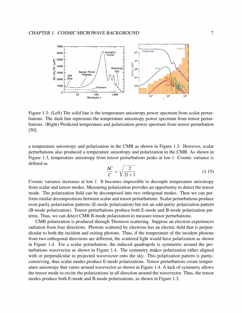
Figure 1.3: (Left) The solid line is the temperature anisotropy power spectrum from scalar pertur-bations. The dash line represents the temperature anisotropy power spectrum from tensor pertur-bations. (Right) Predicted temperature and polarization power spectrum from tensor perturbation[50].
a temperature anisotropy and polarization in the CMB as shown in Figure 1.3. However, scalarperturbations also produced a temperature anisotropy and polarization in the CMB. As shown inFigure 1.3, temperature anisotropy from tensor perturbations peaks at low l. Cosmic variance isdefined as
∆CC
=
√2
2l +1(1.15)
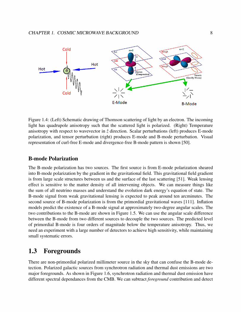
Cosmic variance increases at low l. It becomes impossible to decouple temperature anisotropyfrom scalar and tensor modes. Measuring polarization provides an opportunity to detect the tensormode. The polarization field can be decomposed into two orthogonal modes. Then we can per-form similar decompositions between scalar and tensor perturbations. Scalar perturbations produceeven-parity polarization patterns (E-mode polarization) but not an odd-parity polarization pattern(B-mode polarization). Tensor perturbations produce both E-mode and B-mode polarization pat-terns. Thus, we can detect CMB B-mode polarization to measure tensor perturbations.
CMB polarization is produced through Thomson scattering. Suppose an electron experiencesradiation from four directions. Photons scattered by electrons has an electric field that is perpen-dicular to both the incident and exiting photons. Thus, if the temperature of the incident photonsfrom two orthogonal directions are different, the scattered light would have polarization as shownin Figure 1.4. For a scalar perturbation, the induced quadrupole is symmetric around the per-turbations wavevector as shown in Figure 1.4. The symmetry makes polarization either alignedwith or perpendicular to projected wavevector onto the sky. This polarization pattern is parity-conserving, thus scalar modes produce E-mode polarizations. Tensor perturbations create temper-ature anisotropy that varies around wavevector as shown in Figure 1.4. A lack of symmetry allowsthe tensor mode to excite the polarizations in all direction around the wavevector. Thus, the tensormodes produce both E-mode and B-mode polarizations, as shown in Figure 1.3.
CHAPTER 1. COSMIC MICROWAVE BACKGROUND 8
Figure 1.4: (Left) Schematic drawing of Thomson scattering of light by an electron. The incominglight has quadrupole anisotropy such that the scattered light is polarized. (Right) Temperatureanisotropy with respect to wavevector in z direction. Scalar perturbations (left) produces E-modepolarization, and tensor perturbation (right) produces E-mode and B-mode perturbation. Visualrepresentation of curl-free E-mode and divergence-free B-mode pattern is shown [50].
B-mode PolarizationThe B-mode polarization has two sources. The first source is from E-mode polarization shearedinto B-mode polarization by the gradient in the gravitational field. This gravitational field gradientis from large scale structures between us and the surface of the last scattering [51]. Weak lensingeffect is sensitive to the matter density of all intervening objects. We can measure things likethe sum of all neutrino masses and understand the evolution dark energy’s equation of state. TheB-mode signal from weak gravitational lensing is expected to peak around ten arcminutes. Thesecond source of B-mode polarization is from the primordial gravitational waves [111]. Inflationmodels predict the existence of a B-mode signal at approximately two-degree angular scales. Thetwo contributions to the B-mode are shown in Figure 1.5. We can use the angular scale differencebetween the B-mode from two different sources to decouple the two sources. The predicted levelof primordial B-mode is four orders of magnitude below the temperature anisotropy. Thus, weneed an experiment with a large number of detectors to achieve high sensitivity, while maintainingsmall systematic errors.
1.3 ForegroundsThere are non-primordial polarized millimeter source in the sky that can confuse the B-mode de-tection. Polarized galactic sources from synchrotron radiation and thermal dust emissions are twomajor foregrounds. As shown in Figure 1.6, synchrotron radiation and thermal dust emission havedifferent spectral dependances from the CMB. We can subtract foreground contribution and detect

CHAPTER 1. COSMIC MICROWAVE BACKGROUND 9
Figure 1.5: TT, EE, BB power spectrum is shown. Two contributions to B-mode are shown. B-mode from weak gravitational lensing of E-mode peaks at l ≈ 1000. B-mode from primordialgraviational wave peaks at l ≈ 100. The gray band of primordial gravitational wave contributionto B-mode represents the theoretically predicted amplitudes [50].
Figure 1.6: Antenna temperature of the predicted synchrotron radiation and thermal dust emissionsalong with EE and BB. Assuming r = 0.01 and 2 < l < 20 [19].
CHAPTER 1. COSMIC MICROWAVE BACKGROUND 10
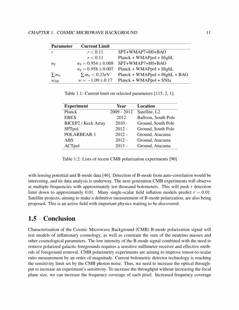
Figure 1.7: Schematic drawing for synchrotron radiation (left) and thermal dust emission (right).For synchrotron radiation, the emitted light is highly polarized. Light is mostly polarized perpen-dicular to the magnetic field. For spinning thermal dust, the dust grains are perpendicular to themagnetic field and its spin axis is parallel to the magnetic field. The emitted radiation is polarizedperpendicular to the magnetic field. [107]
the primordial B-mode by observing at multiple frequency bands.Synchrotron radiation is emitted by accelerating charged particles through galactic magnetic
fields. The synchrotron radiation spectral index is β ≈−3 from WMAP data. Its degree of polar-ization is defined as
P⊥−P‖P⊥+P‖
=p+1
p+7/3(1.16)
Where p is defined as β =−(p+3)/2; thus, the synchrotron radiation polarization fraction couldbe as high as 0.75 and perpendicular to the magnetic field.
The polarized thermal dust emission arises from the alignment of the spin axis of the interstellardust grains along the magnetic field. Thus, it radiates light with polarization also perpendicular tothe magnetic field. It has a rising spectrum as a function of frequency I(ν) ∝ νβ B(T ) where B isbrightness for a given temperature T . We typically model dust emissions with two components:T = 9.5 Kelvin and 16 Kelvin with β = 1.7 and 2.7, respectively. We will get more informationon dust emissions from Planck HFI in the future.
1.4 Current State of FieldThe current upper limit on the tensor-to-scalar ratio is r < 0.11 [115, 2]. This upper limit isset by measurements from temperature anisotropy. The current limits on selected parameters aresummaried in Table 1.1. Currently, each experiment that is taking CMB polarization data containsapproximately one thousand detectors. A list of recently deployed experiments that aim to detectCMB B-mode are in Table 1.2. Recently, lensing B-mode were detected through cross-correlation
CHAPTER 1. COSMIC MICROWAVE BACKGROUND 11
Parameter Current Limitr r < 0.11 SPT+WMAP7+H0+BAO
r < 0.11 Planck + WMAPpol + HighLnS nS = 0.954±0.008 SPT+WMAP7+H0+BAO
nS = 0.958±0.007 Planck + WMAPpol + HighL∑mν ∑mν < 0.23eV Planck + WMAPpol + HighL + BAOwDE w =−1.09±0.17 Planck + WMAPpol + SNIa
Table 1.1: Current limit on selected parameters [115, 2, 1].
Experiment Year LocationPlanck 2009 - 2012 Satellite, L2EBEX 2012 Balloon, South PoleBICEP2 / Keck Array 2010 - Ground, South PoleSPTpol 2012 - Ground, South PolePOLARBEAR-1 2012 - Ground, AtacamaABS 2012 - Ground, AtacamaACTpol 2013 - Ground, Atacama
Table 1.2: Lists of recent CMB polarization experiments [90]
with lensing potential and B-mode data [46]. Detection of B-mode from auto-correlation would beinteresting, and its data analysis is underway. The next generation CMB experiments will observeat multiple frequencies with approximately ten thousand bolometers. This will push r detectionlimit down to approximately 0.01. Many single-scalar field inflation models predict r = 0.01.Satellite projects, aiming to make a definitive measurement of B-mode polarization, are also beingproposed. This is an active field with important physics waiting to be discovered.
1.5 ConclusionCharacterization of the Cosmic Microwave Background (CMB) B-mode polarization signal willtest models of inflationary cosmology, as well as constrain the sum of the neutrino masses andother cosmological parameters. The low intensity of the B-mode signal combined with the need toremove polarized galactic foregrounds requires a sensitive millimeter receiver and effective meth-ods of foreground removal. CMB polarimetry experiments are aiming to improve tensor-to-scalarratio measurement by an order of magnitude. Current bolometric detector technology is reachingthe sensitivity limit set by the CMB photon noise. Thus, we need to increase the optical through-put to increase an experiment’s sensitivity. To increase the throughput without increasing the focalplane size, we can increase the frequency coverage of each pixel. Increased frequency coverage

CHAPTER 1. COSMIC MICROWAVE BACKGROUND 12
per pixel has additional advantage that we can split the signal into frequency bands to obtain spec-tral information. The detection of multiple frequency bands allows for removal of the polarizedforeground emission from synchrotron radiation and thermal dust emission, by utilizing its spectraldependence. Traditionally, spectral information has been captured with a multi-chroic focal planeconsisting of a heterogeneous mix of single-color pixels. To maximize the efficiency of the focalplane area, we developed a multi-chroic pixel. Many next generation CMB experiments will usethe multichroic pixel archtechture to map the CMB with high sensitivity.
13
Chapter 2
POLARBEAR-2
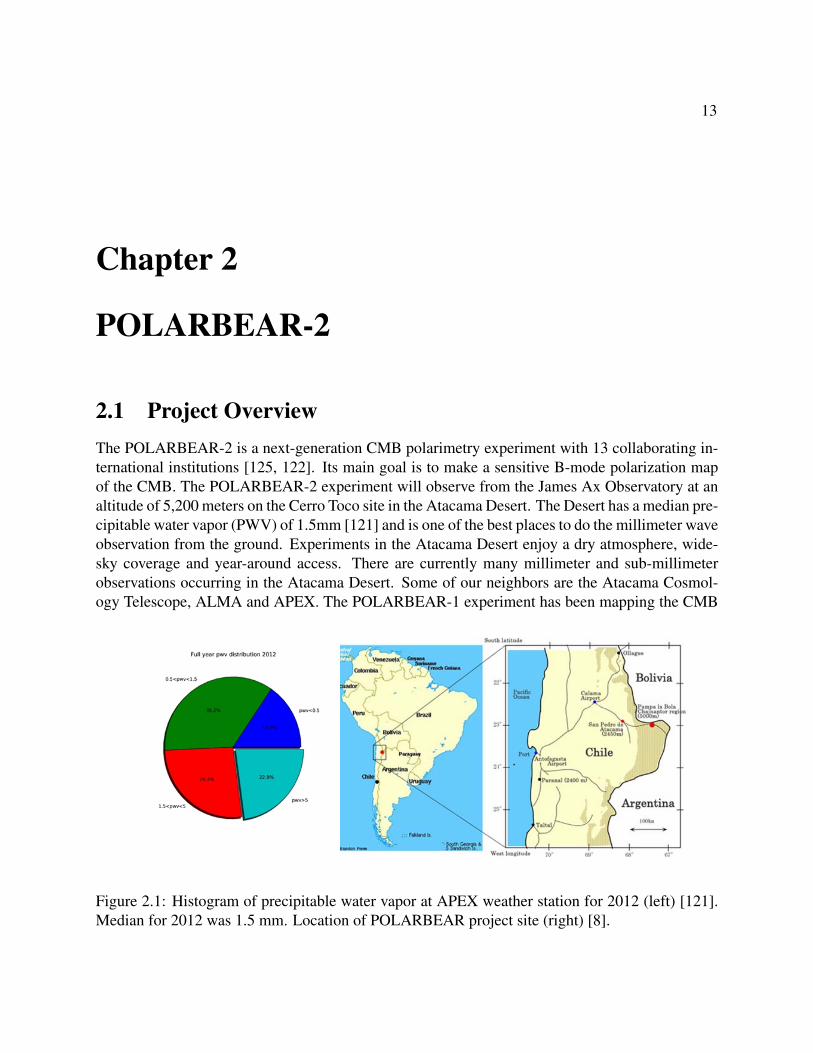
2.1 Project OverviewThe POLARBEAR-2 is a next-generation CMB polarimetry experiment with 13 collaborating in-ternational institutions [125, 122]. Its main goal is to make a sensitive B-mode polarization mapof the CMB. The POLARBEAR-2 experiment will observe from the James Ax Observatory at analtitude of 5,200 meters on the Cerro Toco site in the Atacama Desert. The Desert has a median pre-cipitable water vapor (PWV) of 1.5mm [121] and is one of the best places to do the millimeter waveobservation from the ground. Experiments in the Atacama Desert enjoy a dry atmosphere, wide-sky coverage and year-around access. There are currently many millimeter and sub-millimeterobservations occurring in the Atacama Desert. Some of our neighbors are the Atacama Cosmol-ogy Telescope, ALMA and APEX. The POLARBEAR-1 experiment has been mapping the CMB
Figure 2.1: Histogram of precipitable water vapor at APEX weather station for 2012 (left) [121].Median for 2012 was 1.5 mm. Location of POLARBEAR project site (right) [8].
CHAPTER 2. POLARBEAR-2 14
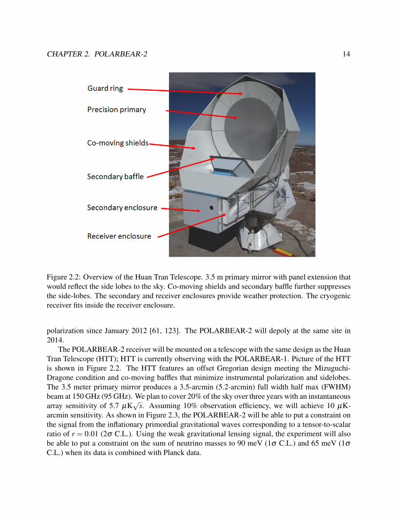
Figure 2.2: Overview of the Huan Tran Telescope. 3.5 m primary mirror with panel extension thatwould reflect the side lobes to the sky. Co-moving shields and secondary baffle further suppressesthe side-lobes. The secondary and receiver enclosures provide weather protection. The cryogenicreceiver fits inside the receiver enclosure.
polarization since January 2012 [61, 123]. The POLARBEAR-2 will depoly at the same site in2014.
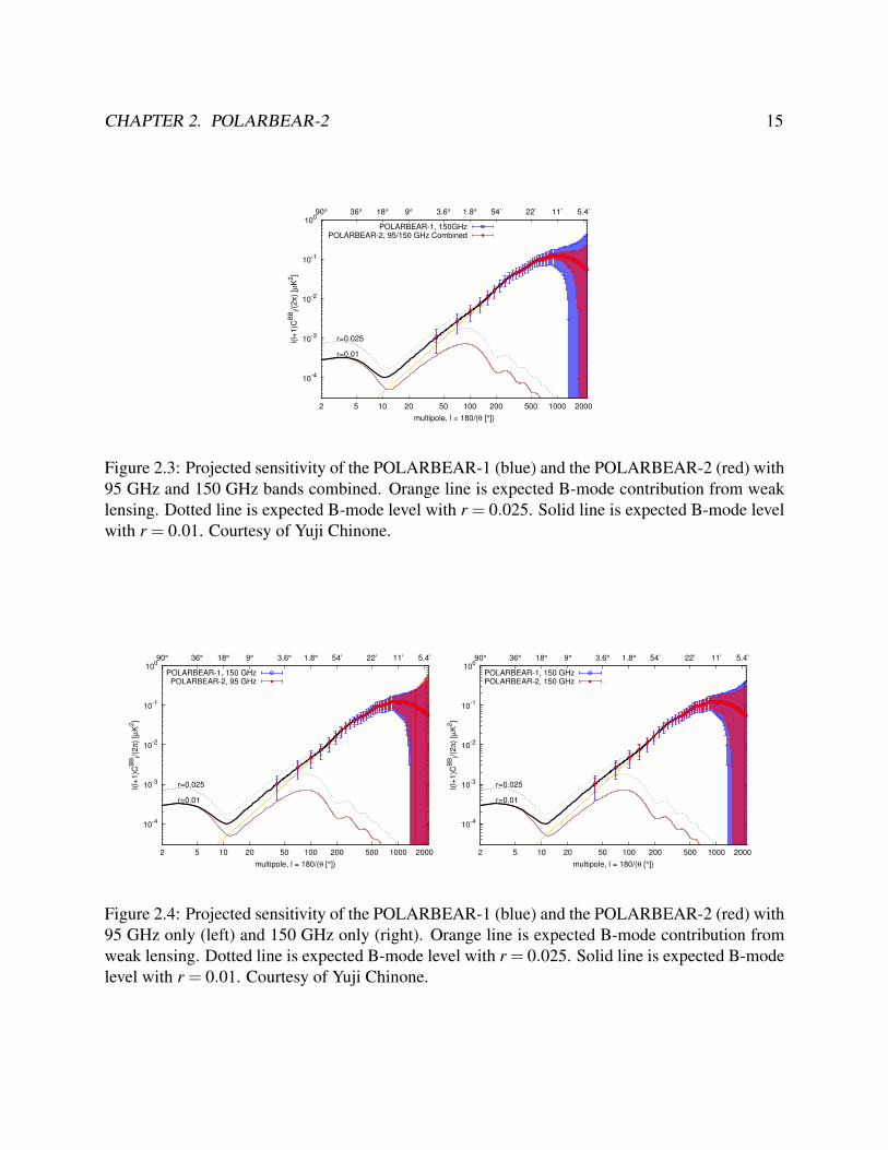
The POLARBEAR-2 receiver will be mounted on a telescope with the same design as the HuanTran Telescope (HTT); HTT is currently observing with the POLARBEAR-1. Picture of the HTTis shown in Figure 2.2. The HTT features an offset Gregorian design meeting the Mizuguchi-Dragone condition and co-moving baffles that minimize instrumental polarization and sidelobes.The 3.5 meter primary mirror produces a 3.5-arcmin (5.2-arcmin) full width half max (FWHM)beam at 150 GHz (95 GHz). We plan to cover 20% of the sky over three years with an instantaneousarray sensitivity of 5.7 µK
√s. Assuming 10% observation efficiency, we will achieve 10 µK-
arcmin sensitivity. As shown in Figure 2.3, the POLARBEAR-2 will be able to put a constraint onthe signal from the inflationary primordial gravitational waves corresponding to a tensor-to-scalarratio of r = 0.01 (2σ C.L.). Using the weak gravitational lensing signal, the experiment will alsobe able to put a constraint on the sum of neutrino masses to 90 meV (1σ C.L.) and 65 meV (1σ
C.L.) when its data is combined with Planck data.
CHAPTER 2. POLARBEAR-2 15
10-4
10-3
10-2
10-1
100
2 5 10 20 50 100 200 500 1000 2000
90° 36° 18° 9° 3.6° 1.8° 54’ 22’ 11’ 5.4’
l(l+
1)C
BB
l/(2
π)
[µK
2]
multipole, l = 180/(θ [°])
POLARBEAR-1, 150GHzPOLARBEAR-2, 95/150 GHz Combined
r=0.025
r=0.01
Figure 2.3: Projected sensitivity of the POLARBEAR-1 (blue) and the POLARBEAR-2 (red) with95 GHz and 150 GHz bands combined. Orange line is expected B-mode contribution from weaklensing. Dotted line is expected B-mode level with r = 0.025. Solid line is expected B-mode levelwith r = 0.01. Courtesy of Yuji Chinone.
10-4
10-3
10-2
10-1
100
2 5 10 20 50 100 200 500 1000 2000
90° 36° 18° 9° 3.6° 1.8° 54’ 22’ 11’ 5.4’
l(l+
1)C
BB
l/(2
π)
[µK
2]
multipole, l = 180/(θ [°])
POLARBEAR-1, 150 GHzPOLARBEAR-2, 95 GHz
r=0.025
r=0.01
10-4
10-3
10-2
10-1
100
2 5 10 20 50 100 200 500 1000 2000
90° 36° 18° 9° 3.6° 1.8° 54’ 22’ 11’ 5.4’
l(l+
1)C
BB
l/(2
π)
[µK
2]
multipole, l = 180/(θ [°])
POLARBEAR-1, 150 GHzPOLARBEAR-2, 150 GHz
r=0.025
r=0.01
Figure 2.4: Projected sensitivity of the POLARBEAR-1 (blue) and the POLARBEAR-2 (red) with95 GHz only (left) and 150 GHz only (right). Orange line is expected B-mode contribution fromweak lensing. Dotted line is expected B-mode level with r = 0.025. Solid line is expected B-modelevel with r = 0.01. Courtesy of Yuji Chinone.
CHAPTER 2. POLARBEAR-2 16
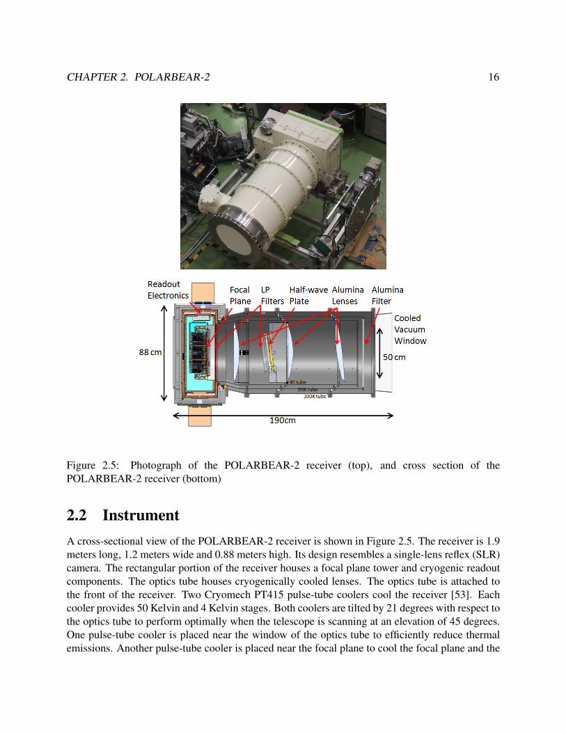
Figure 2.5: Photograph of the POLARBEAR-2 receiver (top), and cross section of thePOLARBEAR-2 receiver (bottom)
2.2 InstrumentA cross-sectional view of the POLARBEAR-2 receiver is shown in Figure 2.5. The receiver is 1.9meters long, 1.2 meters wide and 0.88 meters high. Its design resembles a single-lens reflex (SLR)camera. The rectangular portion of the receiver houses a focal plane tower and cryogenic readoutcomponents. The optics tube houses cryogenically cooled lenses. The optics tube is attached tothe front of the receiver. Two Cryomech PT415 pulse-tube coolers cool the receiver [53]. Eachcooler provides 50 Kelvin and 4 Kelvin stages. Both coolers are tilted by 21 degrees with respect tothe optics tube to perform optimally when the telescope is scanning at an elevation of 45 degrees.One pulse-tube cooler is placed near the window of the optics tube to efficiently reduce thermalemissions. Another pulse-tube cooler is placed near the focal plane to cool the focal plane and the
CHAPTER 2. POLARBEAR-2 17
Figure 2.6: The POLARBEAR-2 receiver with ray tracing. Secondary mirror is shown on right.
readout electronics. Annealed 6-N aluminum strips were epoxied to the receiver shells to increasethe thermal conductivity of the receiver. A three-stage helium sorption refrigerator cools the focalplane tower with 2 Kelvin, 350 milli-Kelvin and 250 milli-Kelvin stages [75].
The ray tracing for the POLARBEAR-2 is shown in Figure 2.6. The optics has a field-of-viewof 4.8 [85]. High purity (99.5%) alumina was used as an infrared filter to reduce the thermalloading from the 500 mm diameter window in the optics tube. Alumina absorbs infrared photonseffectively, yet it is transparent at the millimeter wave. Alumina has three orders of magnitudebetter thermal conductivity at 100 Kelvin than plastics, which are commonly used as dielectricfilters [55].
Three lenses were fabricated from high purity (99.9%) alumina. The high dielectric constantof alumina (εr ≈ 10) allows an optics design with a large field of view with high strehl ratio. Highpurity alumina also has low loss (tanδ ≈ 1× 10⁻⁴). Alumina has high thermal conductivity thathelps with the overall cryogenic performance. However, the high dielectric constant of aluminarequires anti-reflection (AR) coating to minimize the reflection at the dielectric boundary. Sincethe POLARBEAR-2 observes at 95 GHz and 150 GHz simultaneously, the AR coating on the lensmust cover a wide frequency range. We developed a two-layer epoxy-based AR coating [117, 28].Details on lenses material and AR coating development will be discussed in Chapter 3.
We place 4 Kelvin cold stop and an achromatic half-wave plate at the aperture. The cold stopis designed for F/# = 1.9 optics. The achromatic half-wave plate is made from stacks of sapphirecrystals. The half-wave plate rotates on a superconducting bearing to modulate polarized signal toreduce systematic error from the optics [83, 84].
The focal plane is shown on Figure 2.7. The focal plane design was based on the POLARBEAR-1 design. A 365 mm diameter focal plane tower has 2 Kelvin, 350 milli-Kelvin and 250 milli-Kelvin stages. Each stage was isolated by hollowed vespel legs. The focal plane tower housesseven detector array modules. Each module has a hexagonal detector array wafer and readout elec-
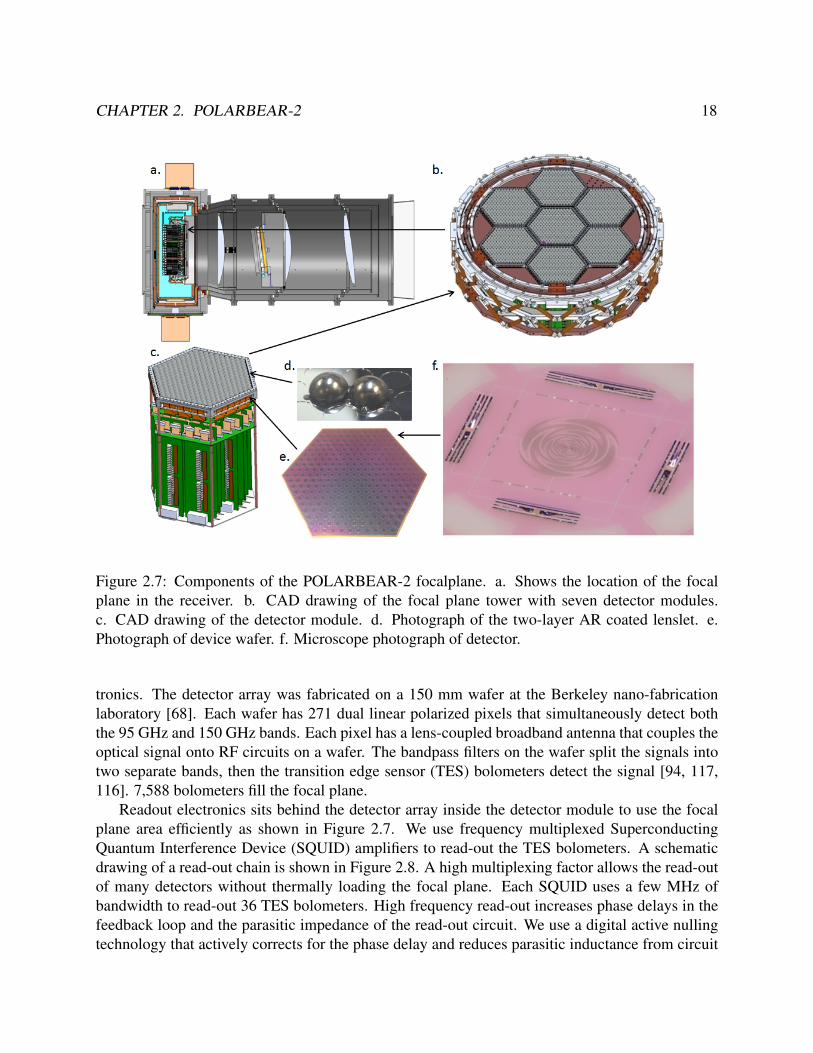
CHAPTER 2. POLARBEAR-2 18
Figure 2.7: Components of the POLARBEAR-2 focalplane. a. Shows the location of the focalplane in the receiver. b. CAD drawing of the focal plane tower with seven detector modules.c. CAD drawing of the detector module. d. Photograph of the two-layer AR coated lenslet. e.Photograph of device wafer. f. Microscope photograph of detector.
tronics. The detector array was fabricated on a 150 mm wafer at the Berkeley nano-fabricationlaboratory [68]. Each wafer has 271 dual linear polarized pixels that simultaneously detect boththe 95 GHz and 150 GHz bands. Each pixel has a lens-coupled broadband antenna that couples theoptical signal onto RF circuits on a wafer. The bandpass filters on the wafer split the signals intotwo separate bands, then the transition edge sensor (TES) bolometers detect the signal [94, 117,116]. 7,588 bolometers fill the focal plane.
Readout electronics sits behind the detector array inside the detector module to use the focalplane area efficiently as shown in Figure 2.7. We use frequency multiplexed SuperconductingQuantum Interference Device (SQUID) amplifiers to read-out the TES bolometers. A schematicdrawing of a read-out chain is shown in Figure 2.8. A high multiplexing factor allows the read-outof many detectors without thermally loading the focal plane. Each SQUID uses a few MHz ofbandwidth to read-out 36 TES bolometers. High frequency read-out increases phase delays in thefeedback loop and the parasitic impedance of the read-out circuit. We use a digital active nullingtechnology that actively corrects for the phase delay and reduces parasitic inductance from circuit
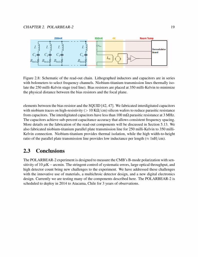
CHAPTER 2. POLARBEAR-2 19
Figure 2.8: Schematic of the read-out chain. Lithographed inductors and capacitors are in serieswith bolometers to select frequency channels. Niobium-titanium transmission lines thermally iso-late the 250 milli-Kelvin stage (red line). Bias resistors are placed at 350 milli-Kelvin to minimizethe physical distance between the bias resistors and the focal plane.
elements between the bias resistor and the SQUID [42, 47]. We fabricated interdigitated capacitorswith niobium traces on high-resistivity (> 10 KΩ/cm) silicon wafers to reduce parasitic resistancefrom capacitors. The interdigitated capacitors have less than 100 mΩ parasitic resistance at 3 MHz.The capacitors achieve sub-percent capacitance accuracy that allows consistent frequency spacing.More details on the fabrication of the read-out components will be discussed in Section 5.13. Wealso fabricated niobium-titanium parallel plate transmission line for 250 milli-Kelvin to 350 milli-Kelvin connection. Niobium-titanium provides thermal isolation, while the high width-to-heightratio of the parallel plate transmission line provides low inductance per length (≈ 1nH/cm).
2.3 ConclusionsThe POLARBEAR-2 experiment is designed to measure the CMB’s B-mode polarization with sen-sitivity of 10 µK− arcmin. The stringent control of systematic errors, large optical throughput, andhigh detector count bring new challenges to the experiment. We have addressed these challengeswith the innovative use of materials, a multichroic detector design, and a new digital electronicsdesign. Currently we are testing many of the components described here. The POLARBEAR-2 isscheduled to deploy in 2014 to Atacama, Chile for 3 years of observations.
20
Chapter 3
Lens Material and Anti-Reflection Coating
3.1 IntroductionThe POLARBEAR-2 has an aggressive receiver optics design that achieves four degrees field-of-view. The POLARBEAR-2 uses a telescope with the same design as the HTT, thus, the opticsdesign effort was focused on the lenses in the cryogenic receiver. We first tried to design lenses withultra-high molecular weight polyethylene (UHMWPE) since that was used for the POLARBEAR-1 receiver [61]. However, we discovered that achieving the required strehl ratio (> 0.8) over the36.5 mm diameter focal plane required the optics tube to be too long to fit into the HTT. Wethen considered using single-crystal high-resistivity silicon as lens material as it has successfullybeen used for the Atacama Cosmology Telescope [37]. High-resistivity silicon has many desirableproperties when used as millimeter wave lens. High-resistivity silicon has a typical loss tangentof 10−5 to low 10−4, and high thermal conductivity to facilitate cooing [78]. Also, its high indexof refraction allows lens to have high lensing power with a large curvature radius. The largestdiameter high-resistivity silicon ingot we were able to find was a 450 mm diameter ingot fromSilfex [112]. We then began designing around the silicon ingot. We found that the length limitof the optics tube from the existing telescope design forced lenses to be larger than 450 mm indiameter. Attempting to design optics around silicon showed us that the high index of refractionwas really beneficial. We looked for materials with similar properties to silicon but that can belarger than 450 mm in diameter. 99.9% pure alumina from Nihon Ceratec met the criteria [76].It has a refraction index of 3.20± 0.01 at room temperature and loss-tangent of (9±2)× 10−5
at 140 Kelvin. It is available up to 1000 mm in diameter, with a maximum thickness of 50 mm.Alumina has high thermal conductivity [55] and is also mechanically very strong - unlike silicon,which is brittle. Receiver optics were successfully designed with three alumina lenses, each havinga diameter of 500 mm and maximum thickness of 50 mm. The receiver cross-section with a raytracing overlay is shown in Figure 2.6. The POLARBEAR-2 uses lenslet-coupled multichroicdetector. For the lenslet, we decided to use single crystal high-resistivity silicon since the detectorwafer was already made out of silicon.
Alumina and silicon are ideal lens materials for cryogenic millimeter-wave optics. However,

CHAPTER 3. LENS MATERIAL AND ANTI-REFLECTION COATING 21
50 100 150 2000
0.2
0.4
0.6
0.8
1
Frequency [GHz]
Tra
nsm
issio
n
tan(δ) = 1× 10⁻⁵
tan(δ) = 5× 10⁻⁵
tan(δ) = 1× 10⁻⁴
tan(δ) = 5× 10⁻⁴
tan(δ) = 1× 10⁻³
0 0.2 0.4 0.6 0.8 1
x 10−3
0.5
1
1.5
2
2.5
3
3.5x 10
10
tan(δ)
Mappin
g S
peed [N
/K−
2⋅ s]
95 GHz
150 GHz
Figure 3.1: (left) Transmission through three 50 mm thick alumina with refraction index of n= 3.2.Fabry-Perot fringes were removed. We assumed that each slab has a two-layer anti-reflectioncoating with a dielectric constant of 2 and 5 on each surface. Each layer of anti-reflection coatinghas thickness of λ/4 at 120 GHz. Loss in anti-reflection coatings were ignored. (right) Mappingspeed as function of loss-tangent of alumina lens. Nominal loading from Table 4.1 and Table 4.2were assumed for 95 GHz and 150 GHz except for efficiency through alumina. Pixel diameter isnominal 6.789 mm.
one downside of the high dielectric constant is the reflection at the vacuum-dielectric interface,which can be as high as 30%. There are many effective AR coatings using a thin dielectric coat-ing, metal-mesh layers or sub-wavelength structures [71, 102, 133, 87]. However, these coatingswill not work for the next generation CMB experiments with multichroic detectors. Most reportedmillimeter-wave, dielectric-based AR coatings are single layer and, thus, limited to narrow band-widths. A single-layer coating for our application would have a 41% fractional bandwidth withless than 10% reflection. We have developed a multilayer epoxy-based dielectric AR coating withmore than 90% fractional bandwidth. While multilayer dielectric coatings have been developedin the past [102, 105, 108], our innovative, moldable adhesive coatings are applicable for high di-electric constant curved lenses. We have demonstrated these coatings on small lenslets and 50 mmdiameter flat surfaces and believe that this approach may be extended for 500 mm lenses. Addi-tionally, we can tune the dielectric constant of our layers, which allows for the broad application ofour coatings. AR coating development was previously published by Suzuki and Rosen [117, 28].We provide more details about developing the AR coating in this chapter.

CHAPTER 3. LENS MATERIAL AND ANTI-REFLECTION COATING 22
tan(δ ) 95 GHz band 150 GHz band1×10−5 97.3% 95.5%5×10⁻⁵ 93.8% 90.4%1×10⁻⁴ 89.5% 84.1%5×10⁻⁴ 61.9% 47.2%1×10⁻³ 39.1% 22.9%
Table 3.1: Transmission through three 50 mm alumina lenses for 95 GHz band and 150 GHz band.We assume each slab has two-layer anti-reflection coating with dielectric constant of 2 and 5 onboth surface. Each layer of anti-reflection coating has thickness of λ/4 at 120 GHz. Loss inanti-reflection coatings were ignored.
3.2 Material Development
Material DevelopmentTo study absorption loss, we looked at the loss-tangent (tan(δ )) of the material. The loss-tangentis defined as the tangent of an angle between the real and imaginary dielectric constant of thematerial tan(δ ) = Im(ε)/Re(ε). We can calculate the propagation constant (γ) of plane wavetraveling through a medium with dielectric constant of ε .
E0e−iγz (3.1)
Where E0 is an amplitude of an electric field at z = 0. z is a distance that wave traveled in medium.Attenuation factor is Im(γ). We can write γ with explicitly using tan(δ ) as
γ = ω√
µRe(ε)(1− i tan(δ )) (3.2)
We plotted the expected loss as function of tan(δ ) of alumina in Figure 3.1. Plot assumes planewave traveling through three 50 mm alumina lens with dielectric constant of 10.2. We also assumedtwo-layer anti-reflection coating on both sides of all lenses. Calculated in-band transmission weretabulated on Table 3.1. Figure 5.32 shows expected mapping speed as a function of tan(δ ). Sinceloss in mapping speed was steep function of tan(δ ), we set a criteria that lens material needs tohave tan(δ )< 1×10⁻⁴.
We varied the refraction index of the lens of each design to determine how accurate we need toknow the refraction index. We then looked at how the strehl ratio degraded as a function of how therefraction index deviated from its designed value. From this test, we determined that the refractionindex needs to be measured to within 1% accuracy.
MeasurementWe obtained three types of aluminas from Nihon Ceratec. We studied 99.5% LD purity alumina,99.9% purity alumina and APJF alumina, which has a different sintering process and produces
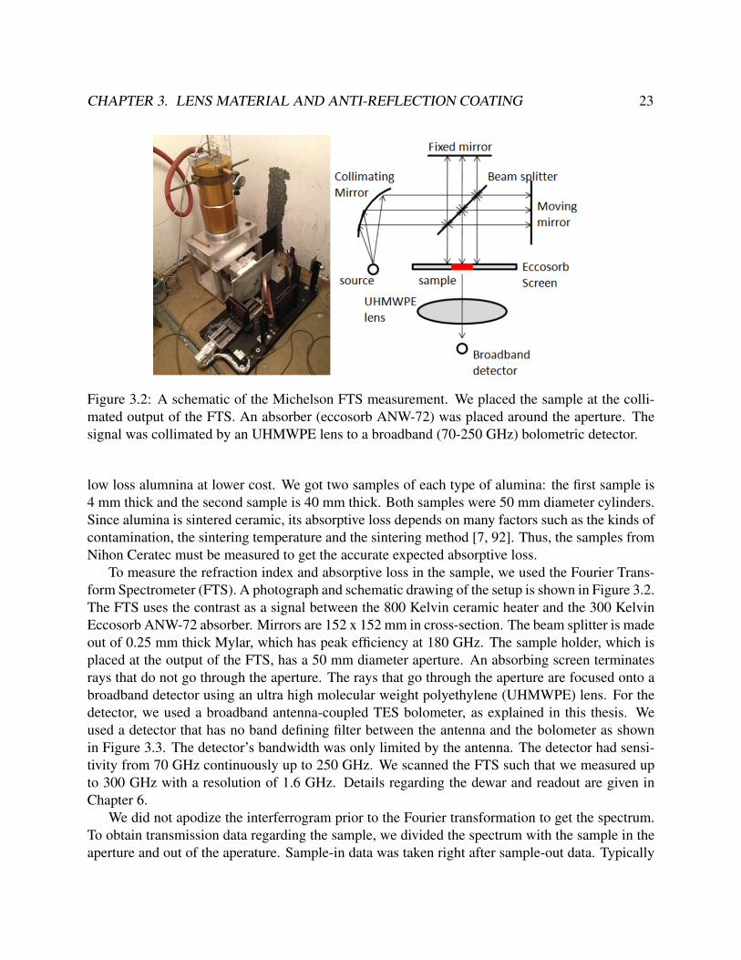
CHAPTER 3. LENS MATERIAL AND ANTI-REFLECTION COATING 23
Figure 3.2: A schematic of the Michelson FTS measurement. We placed the sample at the colli-mated output of the FTS. An absorber (eccosorb ANW-72) was placed around the aperture. Thesignal was collimated by an UHMWPE lens to a broadband (70-250 GHz) bolometric detector.
low loss alumnina at lower cost. We got two samples of each type of alumina: the first sample is4 mm thick and the second sample is 40 mm thick. Both samples were 50 mm diameter cylinders.Since alumina is sintered ceramic, its absorptive loss depends on many factors such as the kinds ofcontamination, the sintering temperature and the sintering method [7, 92]. Thus, the samples fromNihon Ceratec must be measured to get the accurate expected absorptive loss.
To measure the refraction index and absorptive loss in the sample, we used the Fourier Trans-form Spectrometer (FTS). A photograph and schematic drawing of the setup is shown in Figure 3.2.The FTS uses the contrast as a signal between the 800 Kelvin ceramic heater and the 300 KelvinEccosorb ANW-72 absorber. Mirrors are 152 x 152 mm in cross-section. The beam splitter is madeout of 0.25 mm thick Mylar, which has peak efficiency at 180 GHz. The sample holder, which isplaced at the output of the FTS, has a 50 mm diameter aperture. An absorbing screen terminatesrays that do not go through the aperture. The rays that go through the aperture are focused onto abroadband detector using an ultra high molecular weight polyethylene (UHMWPE) lens. For thedetector, we used a broadband antenna-coupled TES bolometer, as explained in this thesis. Weused a detector that has no band defining filter between the antenna and the bolometer as shownin Figure 3.3. The detector’s bandwidth was only limited by the antenna. The detector had sensi-tivity from 70 GHz continuously up to 250 GHz. We scanned the FTS such that we measured upto 300 GHz with a resolution of 1.6 GHz. Details regarding the dewar and readout are given inChapter 6.
We did not apodize the interferrogram prior to the Fourier transformation to get the spectrum.To obtain transmission data regarding the sample, we divided the spectrum with the sample in theaperture and out of the aperature. Sample-in data was taken right after sample-out data. Typically
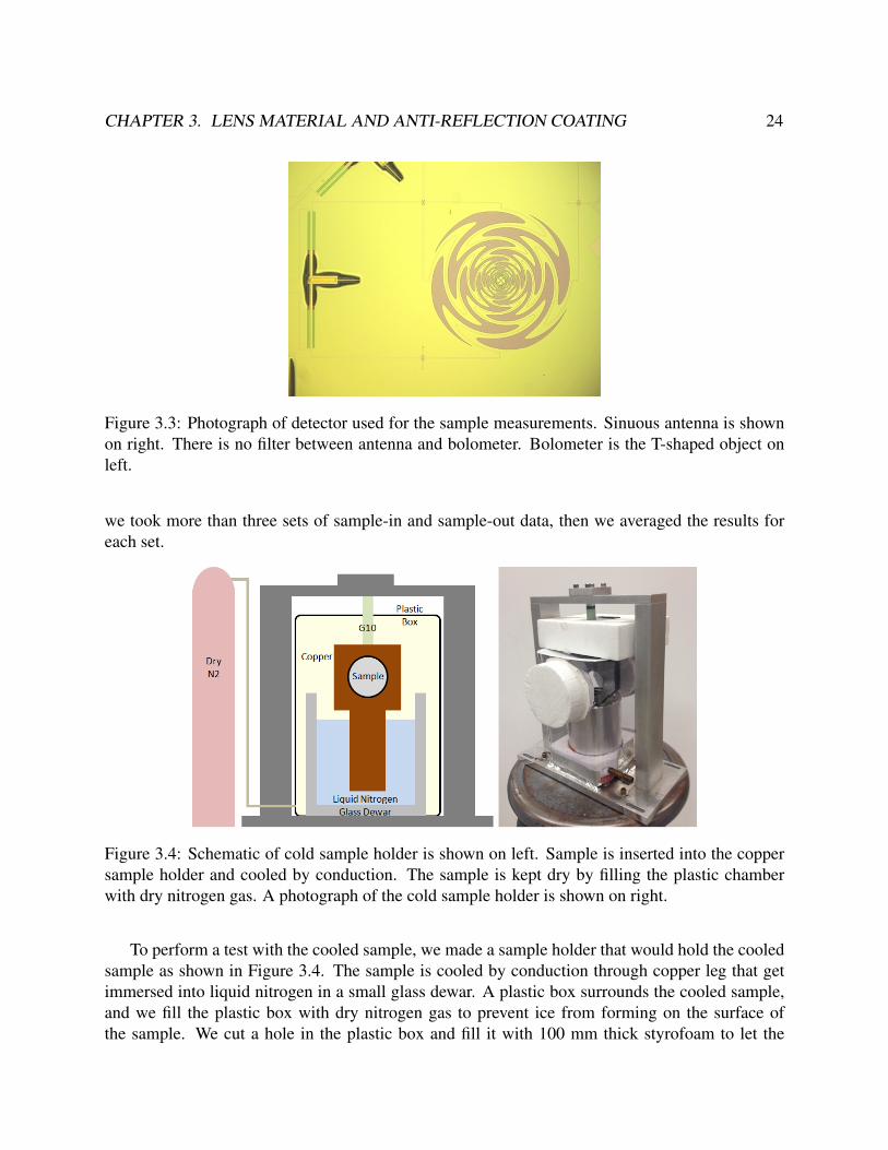
CHAPTER 3. LENS MATERIAL AND ANTI-REFLECTION COATING 24
Figure 3.3: Photograph of detector used for the sample measurements. Sinuous antenna is shownon right. There is no filter between antenna and bolometer. Bolometer is the T-shaped object onleft.
we took more than three sets of sample-in and sample-out data, then we averaged the results foreach set.
Figure 3.4: Schematic of cold sample holder is shown on left. Sample is inserted into the coppersample holder and cooled by conduction. The sample is kept dry by filling the plastic chamberwith dry nitrogen gas. A photograph of the cold sample holder is shown on right.
To perform a test with the cooled sample, we made a sample holder that would hold the cooledsample as shown in Figure 3.4. The sample is cooled by conduction through copper leg that getimmersed into liquid nitrogen in a small glass dewar. A plastic box surrounds the cooled sample,and we fill the plastic box with dry nitrogen gas to prevent ice from forming on the surface ofthe sample. We cut a hole in the plastic box and fill it with 100 mm thick styrofoam to let the
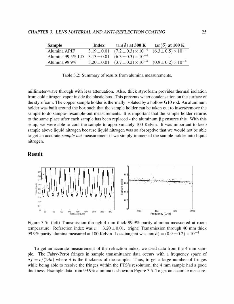
CHAPTER 3. LENS MATERIAL AND ANTI-REFLECTION COATING 25
Sample Index tan(δ ) at 300 K tan(δ ) at 100 KAlumina APJF 3.19±0.01 (7.2±0.3)×10−4 (6.3±0.5)×10−4
Alumina 99.5% LD 3.13±0.01 (6.3±0.3)×10−4 -Alumina 99.9% 3.20±0.01 (3.7±0.2)×10−4 (0.9±0.2)×10−4
Table 3.2: Summary of results from alumina measurements.
millimeter-wave through with less attenuation. Also, thick styrofoam provides thermal isolationfrom cold nitrogen vapor inside the plastic box. This prevents water condensation on the surface ofthe styrofoam. The copper sample holder is thermally isolated by a hollow G10 rod. An aluminumholder was built around the box such that the sample holder can be taken out to insert/remove thesample to do sample-in/sample-out measurements. It is important that the sample holder returnsto the same place after each sample has been replaced - the aluminum jig ensures this. With thissetup, we were able to cool the sample to approximately 100 Kelvin. It was important to keepsample above liquid nitrogen because liquid nitrogen was so absorptive that we would not be ableto get an accurate sample out measurement if we simply immersed the sample holder into liquidnitrogen.
Result
80 100 120 140 160 180 200 220 2400
0.1
0.2
0.3
0.4
0.5
0.6
0.7
0.8
0.9
1
Frequency [GHz]
Tra
nsm
issio
n
100 150 200 2500
0.2
0.4
0.6
0.8
1
Frequency [GHz]
Tra
nsm
issio
n
Figure 3.5: (left) Transmission through 4 mm thick 99.9% purity alumina measuered at roomtemperature. Refraction index was n = 3.20± 0.01. (right) Transmission through 40 mm thick99.9% purity alumina measured at 100 Kelvin. Loss-tangent was tan(δ ) = (0.9±0.2)×10−4.
To get an accurate measurement of the refraction index, we used data from the 4 mm sam-ple. The Fabry-Perot fringes in sample transmittance data occurs with a frequency space of∆ f = c/(2dn) where d is the thickness of the sample. Thus, to get a large number of fringeswhile being able to resolve the fringes within the FTS’s resolution, the 4 mm sample had a goodthickness. Example data from 99.9% alumina is shown in Figure 3.5. To get an accurate measure-

CHAPTER 3. LENS MATERIAL AND ANTI-REFLECTION COATING 26
ment for tan(δ ), we used 40 mm sample. Since tan(δ ) we are after is small, we needed a thickersample to measure the loss.
Figure 3.6: Schematic for characteristic method calculation. E+n and E−n are incoming and reflected
electric field at layer n respectively. [49]
For refraction index calculations, we fitted the data with an analytical model obtained withthe characteristic matrix method [95, 49]. As shown in Figure 3.6, the electric field incident on amultilayer stack is related to the outgoing electric field by(
E+0
E−0
)=
N
∏j=0
D j
t j
(E+
N+1E−N+1
)(3.3)
Where
D j =
(Xi j 00 X−1
i j
)(1 r jr j 1
), i = j−1 (3.4)
where Xi j = exp[iγdi j] describes the propagation of the field between boundary i and j throughdielectric with thickness di j. ti and ri are the Fresnel transmission and reflection coefficient atboundary i, respectively. The material we used was so thick that the fringe spacing was too narrowto resolve with the FTS. Each data point in the spectrum data provides an average of multiplefringes - so only its slope provides useful information. To calculate tan(δ ) for the material, we used
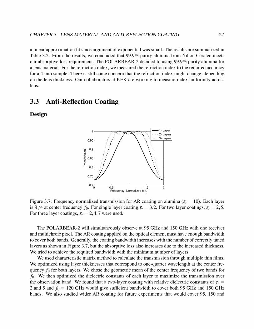
CHAPTER 3. LENS MATERIAL AND ANTI-REFLECTION COATING 27
a linear approximation fit since argument of exponential was small. The results are summarized inTable 3.2. From the results, we concluded that 99.9% purity alumina from Nihon Ceratec meetsour absorptive loss requirement. The POLARBEAR-2 decided to using 99.9% purity alumina fora lens material. For the refraction index, we measured the refraction index to the required accuracyfor a 4 mm sample. There is still some concern that the refraction index might change, dependingon the lens thickness. Our collaborators at KEK are working to measure index uniformity acrosslens.
3.3 Anti-Reflection Coating
Design
0 0.5 1 1.5 20.7
0.75
0.8
0.85
0.9
0.95
1
Frequency, Normalized to f0
Tra
nsm
issio
n
1−Layer
2−Layers
3−Layers
Figure 3.7: Frequency normalized transmission for AR coating on alumina (εr = 10). Each layeris λ/4 at center frequency f0. For single layer coating εr = 3.2. For two layer coatings, εr = 2,5.For three layer coatings, εr = 2,4,7 were used.
The POLARBEAR-2 will simultaneously observe at 95 GHz and 150 GHz with one receiverand multichroic pixel. The AR coating applied on the optical element must have enough bandwidthto cover both bands. Generally, the coating bandwidth increases with the number of correctly tunedlayers as shown in Figure 3.7, but the absorptive loss also increases due to the increased thickness.We tried to achieve the required bandwidth with the minimum number of layers.
We used characteristic matrix method to calculate the transmission through multiple thin films.We optimized using layer thicknesses that correspond to one-quarter wavelength at the center fre-quency f0 for both layers. We chose the geometric mean of the center frequency of two bands forf0. We then optimized the dielectric constants of each layer to maximize the transmission overthe observation band. We found that a two-layer coating with relative dielectric constants of εr =2 and 5 and f0 = 120 GHz would give sufficient bandwidth to cover both 95 GHz and 150 GHzbands. We also studied wider AR coating for future experiments that would cover 95, 150 and

CHAPTER 3. LENS MATERIAL AND ANTI-REFLECTION COATING 28
220 GHz bands simultaneously. We found that a three-layer coating, centered around 150 GHzwith dielectric constants of εr = 2, 4, and 7, would have acceptable bandwidth.
Coating MaterialFor the coating material, we wanted a material that would conform to a highly curved surface, ad-here without any additional layer, withstand thermal cycling and have a tunable dielectric constantto achieve the optimal dielectric constant. We chose epoxy as the base material for its adhesionproperties and malleability. We referred to Lamb for the approximate dielectric constants of epox-ies [69]. To measure dielectric constants and absorption losses, we used the same method that wasused to measure alumina’s dielectric constant and loss.
We mixed Emerson and Cuming’s Stycast 1090, Stycast 1266A and Stycast 2850FT with theircorresponding catalysts - Catalyst 9, Stycast 1266B and Catalyst 23LV respectively. For the mixingratio, we followed each product’s data sheets and avoided mixing more than 100 mL of sample ata time as heat from the exothermic reaction hardens the mixture too quickly for our application.Cylindrical aluminum molds 25 mm deep and 50 mm in diameter were coated with Mann EaseRelease 200 mold release. We poured the mixture into the mold, then placed the mold in a 90Coven for a few hours.
We cut the cured samples to 6 mm thick and machined both sides to be parallel within 0.1 mm.We finished the surface of the sample with 400 grit sand paper. We then measured its dielectricconstants using the FTS. We found that Stycast 1090, Stycast 1266A and Stycast 2850FT havedielectric constants of 2.06, 2.60 and 4.95, respectively. We successfully obtained mixtures withintermediate dielectric constants by mixing two types of epoxy. To obtain a dielectric constanthigher than 4.95, we mixed Stycast 2850FT with SrTiO3 powder from Fisher Scientific which hasbeen shown to have a high dielectric constant at lower frequencies up to 10 GHz [72]. We triedother high dielectric constant powder such as TiO2 and BaTiO3. These dielectric powders havehigh dielectric constant at lower frequency, but we suspect that its dielectric constant relaxed at100 GHz. Also mixing dielectric powder made epoxy very thick with small amount of powder.Thus powder needed to have very high dielectric constant to be effective. For these high dielectricmixtures, we vacuum-pumped the mixture for 5 minutes to remove air bubbles. With a Stycast2850FT and SrTiO3 mixture, we obtained dielectric constants as high as 7.44. We summarize theresults in Figure 3.8.
Anti-Reflection CoatingTo test AR-coating performance, we AR-coated cylindrical 99.5%-RF pure alumina samples fromCoorstek as shown in Figure 3.9. The alumina sample have a dielectric constant of 9.6 and were51 mm in diameter and 6.35 mm thick. For better adhesion, we lightly sanded the surface ofthe alumina sample with 400 grit sand paper prior to applying the coatings. We prepared epoxymixtures as described in Section 3.2 and then applied a thin layer of the mixture on the aluminasample by pouring this mixture onto the alumina. After the mixture cured, we sanded down eachlayer to 25 µm thickness accuracy before applying next layer. The thickness of each coating layer

CHAPTER 3. LENS MATERIAL AND ANTI-REFLECTION COATING 29
Figure 3.8: Dielectric constants of various epoxy and SrTiO3 mixtures at room temperature as afunction of the percent by weight of the total mixture.
Figure 3.9: Photograph of two-layer AR coated alumina sample. AR coating is applied on bothside. Sample is 6 mm thick and 50 mm in diameter. Coatings were 354 µm, and 224 µm forStycast 1090 layer and Stycast 2850FT layer respectively
corresponds to 354 µm, 250 µm, 224 µm, and 189 µm for dielectric constants of 2, 4, 5, and 7respectively. For an expedited curing process, we placed the samples in a 90C oven for a fewhours. However, the highest dielectric layer with Stycast 2850FT and SrTiO3 was difficult to sandwhen fully cured. For a coating with this mixture, we removed the sample from the oven after 45minutes to sand the surface before it had completely cured.
We measured transmission as a function of frequency using the FTS. Transmittance plots fortwo-layer and three-layer coatings are shown in Figure 3.10. The measurement shows uncoatedalumina which has high Fabry-Perot fringes due to high reflection, whereas the coated sample hashigh transmittance over a wide band. The modeled curve assumed a constant loss tangent at 150GHz. The agreement between theory and measurement is good with a difference consistent withan increase in the loss tangent with frequency, a typical loss trend for epoxies in the millimeter

CHAPTER 3. LENS MATERIAL AND ANTI-REFLECTION COATING 30
range [69].Cooling the samples reduced the band-integrated absorption loss from 15% to less than 1% for
the two-layer coating and from 21% to 10% for the three-layer coating. The larger loss for thethree-layer coating can be attributed to the thicker epoxy layers and high absorption in strontiumtitanate. However, in typical CMB experiments, lenses operate around 4 Kelvin. Because theloss tangent decreases with temperature for many materials [69], we expect better performance atoperating temperatures.
As shown in Figure 3.10, the reflection was suppressed to below 10% over 92% and 104%fractional bandwidth for the two-layer and three-layer coatings, respectively. To calculate thebandwidth of low reflection for the three-layer coating, we corrected for this loss and measured thefractional bandwidth above 90% transmittance. This bandwidth can be visualized by observingthe frequency range over which the transmittance appears relatively flat. This is only 12% greaterthan the two-layer coating bandwidth although theory predicts a difference of 25%. However, thetheoretical band for the three-layer coating extends lower than our setup accurately detects. Thus,the coating itself may have a wider bandwidth than we were able to detect.
80 100 120 140 160 180 200 220 2400
0.2
0.4
0.6
0.8
1
Frequency [GHz]
Tra
nsm
issi
on
300 Kelvin 140 Kelvin Theory Uncoated Alumina
80 100 120 140 160 180 200 220 2400
0.2
0.4
0.6
0.8
1
Frequency [GHz]
Tra
nsm
issi
on
300 Kelvin 140 Kelvin Theory Uncoated Alumina
Figure 3.10: Transmittance spectra of two-layer (top) and three-layer (bottom) AR coated alu-mina at 300 Kelvin (solid black) and 140 Kelvin (dashed red), the modeled curve at 300 Kelvin(dash-dotted blue), and uncoated alumina (dotted magenta). A widened transmittance band can beinferred from the lack of Fabry-Perot fringes.
3.4 Lenslet CoatingTo make a sufficiently precise AR coating on a lens, we designed a mold with a cavity that leavesa thin gap between the lens and mold as shown in Figure 3.11. The cavity was made using aprecision machined, ball-ended mill. We machined a small indentation in a piston to hold thelenslette in place. We made a piston and cavity with two dissimilar metals to prevent gallingbetween pieces. We were able to create coatings with a thickness variation within 25 µm, whichis approximately 10% of the thickness of each layer. The performance degredation from the 10%error in thickness was negligible. We sprayed the cavity with mold release, and then filled thecavity with the appropriate amount of mixed epoxy to fill down to 20 degrees from the flat surface
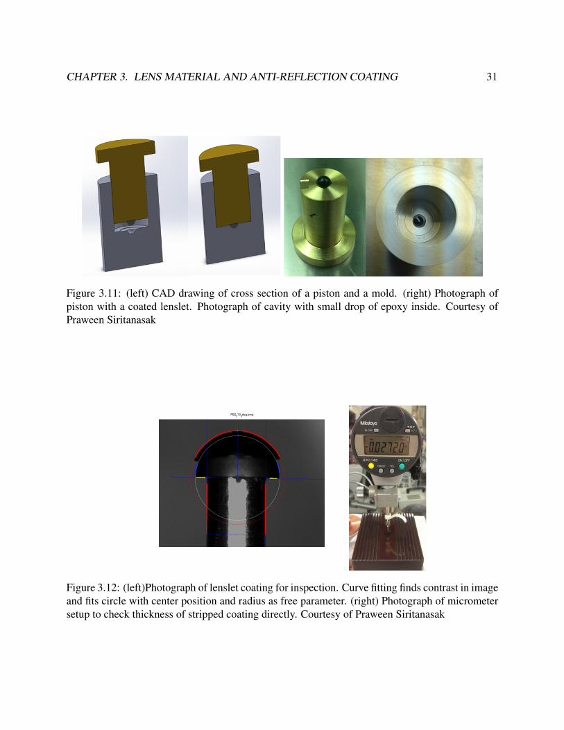
CHAPTER 3. LENS MATERIAL AND ANTI-REFLECTION COATING 31
Figure 3.11: (left) CAD drawing of cross section of a piston and a mold. (right) Photograph ofpiston with a coated lenslet. Photograph of cavity with small drop of epoxy inside. Courtesy ofPraween Siritanasak
PB2270
0deg.bmp
Figure 3.12: (left)Photograph of lenslet coating for inspection. Curve fitting finds contrast in imageand fits circle with center position and radius as free parameter. (right) Photograph of micrometersetup to check thickness of stripped coating directly. Courtesy of Praween Siritanasak

CHAPTER 3. LENS MATERIAL AND ANTI-REFLECTION COATING 32
of the lenslet as shown in Figure 3.11. For additional layers, we repeated the process using moldswith different spacing.
We assessed the quality of the coatings by taking photographs of the side profile and fittingthe surface to the expected circular shape as shown in Figure 3.12. From the fit, we verified thatthe diameter of the coatings was within 25 µm and translation errors were within 25 µm in alldirections. We also confirmed the accuracy by removing the AR coating from mold-release coatedlenslets and measuring directly with micrometers. Our tolerance corresponds to approximately10% of a single layer’s thickness, which would result in less than a 1% decrease in transmittance.
To test cryogenic adhesion, we made twelve two-layer coated 6.35 mm diameter lenses. Wekept one sample as a control and slowly cooled nine samples in a vacuum to liquid nitrogen tem-perature. These nine samples all survived ten slow thermal cycles in the dewar and 18 dunksin liquid nitrogen, returning to room temperature between dunks. Two additional samples wererapidly thermal cycled between room temperature and liquid nitrogen temperature until failure.Failure for one sample occurred after 18 dunks and the other after 50 dunks. There was no changeto the control sample that was kept at room temperature. Since this test, we made many 2-layercoated lenslet-arrays as shown in Figure 5.40, and successfully thermal cycled them. Addition-ally, the optical properties of the two-layer coating have been cold tested multiple times withouta detectable change in performance. We concluded that the coatings have sufficient optical andmechanical stability for our applications.
Anti-Reflection Coating on Large SurfaceWe tried to extend this AR coating technique to a larger surface to coat alumina lenses. However,we noticed that coating on a large surface delaminated at cryogenic temperatures. We solved theproblem by making a 40 µm wide slit in the AR coating. The slit was made in a 2 inch by 2 inchpattern. Even though this solved the delaminating issue, we have not evaluated how this wouldaffect the polarization of transmitted light. Alternative ideas for AR coating over large surfaces arediscussed in Section 7.2 as potential future projects.
3.5 ConclusionBy devising methods to tune the dielectric constant of a mixture between 2.06 and 7.44, we havecreated an effective epoxy-based, broadband anti-reflection coating for millimeter-wave optics.We reduced the reflection from an alumina slab to less than 10% over 92% and 104% fractionalbandwidths with the respective two-layer and three-layer anti-reflection coatings. When sampleswere cooled to 100 Kelvin, the absorptive loss was suppressed to less than 1% in the two-layercoating and 10% in the three-layer coating. Using a precise molding technique, we achieved high-precision coating application to a curved surface. We also demonstrated that the coatings cansurvive numerous thermal cycles. Coating over a large, flat surface has proven to be difficult.There is a proposed solution to segment the AR coating into smaller sections, but its effect onpolarization at the millimeter wave needs to be studied in detail.
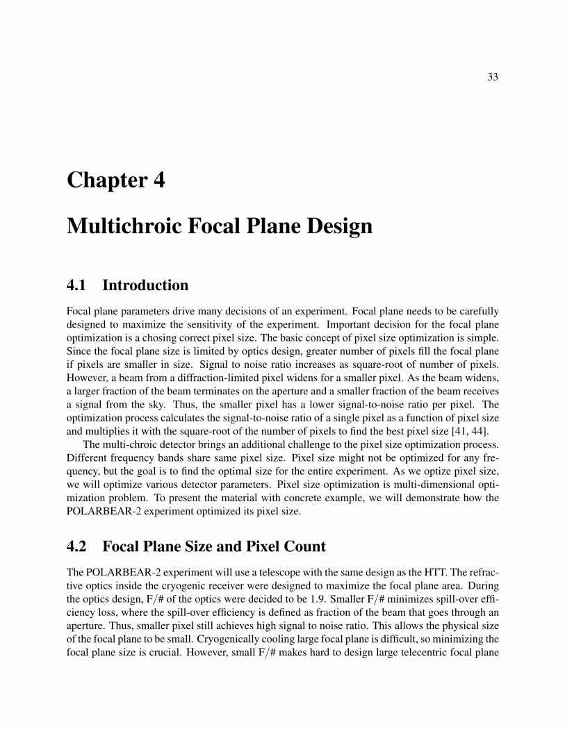
33
Chapter 4
Multichroic Focal Plane Design
4.1 IntroductionFocal plane parameters drive many decisions of an experiment. Focal plane needs to be carefullydesigned to maximize the sensitivity of the experiment. Important decision for the focal planeoptimization is a chosing correct pixel size. The basic concept of pixel size optimization is simple.Since the focal plane size is limited by optics design, greater number of pixels fill the focal planeif pixels are smaller in size. Signal to noise ratio increases as square-root of number of pixels.However, a beam from a diffraction-limited pixel widens for a smaller pixel. As the beam widens,a larger fraction of the beam terminates on the aperture and a smaller fraction of the beam receivesa signal from the sky. Thus, the smaller pixel has a lower signal-to-noise ratio per pixel. Theoptimization process calculates the signal-to-noise ratio of a single pixel as a function of pixel sizeand multiplies it with the square-root of the number of pixels to find the best pixel size [41, 44].
The multi-chroic detector brings an additional challenge to the pixel size optimization process.Different frequency bands share same pixel size. Pixel size might not be optimized for any fre-quency, but the goal is to find the optimal size for the entire experiment. As we optize pixel size,we will optimize various detector parameters. Pixel size optimization is multi-dimensional opti-mization problem. To present the material with concrete example, we will demonstrate how thePOLARBEAR-2 experiment optimized its pixel size.
4.2 Focal Plane Size and Pixel CountThe POLARBEAR-2 experiment will use a telescope with the same design as the HTT. The refrac-tive optics inside the cryogenic receiver were designed to maximize the focal plane area. Duringthe optics design, F/# of the optics were decided to be 1.9. Smaller F/# minimizes spill-over effi-ciency loss, where the spill-over efficiency is defined as fraction of the beam that goes through anaperture. Thus, smaller pixel still achieves high signal to noise ratio. This allows the physical sizeof the focal plane to be small. Cryogenically cooling large focal plane is difficult, so minimizing thefocal plane size is crucial. However, small F/# makes hard to design large telecentric focal plane

CHAPTER 4. MULTICHROIC FOCAL PLANE DESIGN 34
Figure 4.1: CAD drawing of focal plane planning. Circle represent 365 mm available focal planearea. Hexagon is 120 mm side to side.
with diffraction-limited rays. High F/# optics makes optics tube longer. For the POLARBEAR-2,we were running into size constraint from the HTT. Thus, for the POLARBEAR-2 experiment, wedecided that F/# = 1.9 as a compromise. That gave an acceptable strehl ratio (< 0.8) for a focalplane diameter of 365 mm.
We chose a close-packed hexagonal pattern to maximally fill the 365 millimeter diameter focalplane with least number of wafers. We used seven hexagonal-shaped wafers with side-to-sidesize length of 120 mm as shown in Figure 4.1. We reserve approximately 10 mm for hardware.Available side-to-side hexagonal size is S = 110 mm. The total area available (Aavailable) for pixelsare:
Aavailable = Nwa f er
√3
2S2(
16
)π√
3 (4.1)
Where we first calculated the area of Nwa f er hexagon with a side-to-side length of S. Then wemultiplied by a factor to extract an area that will be available for close packed circular pixel.Suppose each pixel has a diameter of D mm, then the area per pixel would be Apixel =
πD2
4 . Numberof pixel is then
Npixel =Aavailable
Apixel= Nwa f er
√3
2S2(
16
)π√
34
πD2 = Nwa f erS2
D2 (4.2)
Number of pixels as a function of pixel size is shown in Figure 4.2.
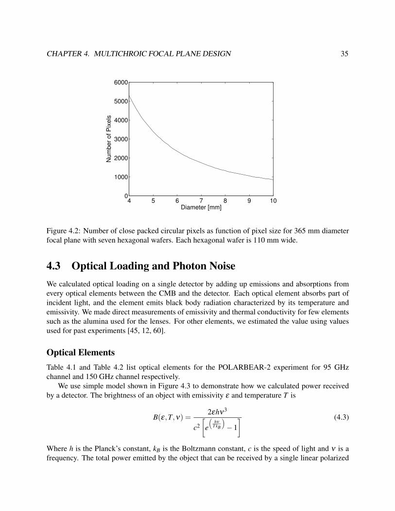
CHAPTER 4. MULTICHROIC FOCAL PLANE DESIGN 35
4 5 6 7 8 9 100
1000
2000
3000
4000
5000
6000
Diameter [mm]
Num
ber
of P
ixels
Figure 4.2: Number of close packed circular pixels as function of pixel size for 365 mm diameterfocal plane with seven hexagonal wafers. Each hexagonal wafer is 110 mm wide.
4.3 Optical Loading and Photon NoiseWe calculated optical loading on a single detector by adding up emissions and absorptions fromevery optical elements between the CMB and the detector. Each optical element absorbs part ofincident light, and the element emits black body radiation characterized by its temperature andemissivity. We made direct measurements of emissivity and thermal conductivity for few elementssuch as the alumina used for the lenses. For other elements, we estimated the value using valuesused for past experiments [45, 12, 60].
Optical ElementsTable 4.1 and Table 4.2 list optical elements for the POLARBEAR-2 experiment for 95 GHzchannel and 150 GHz channel respectively.
We use simple model shown in Figure 4.3 to demonstrate how we calculated power receivedby a detector. The brightness of an object with emissivity ε and temperature T is
B(ε,T,ν) =2εhν3
c2[
e(
hν
T kB
)−1] (4.3)
Where h is the Planck’s constant, kB is the Boltzmann constant, c is the speed of light and ν is afrequency. The total power emitted by the object that can be received by a single linear polarized
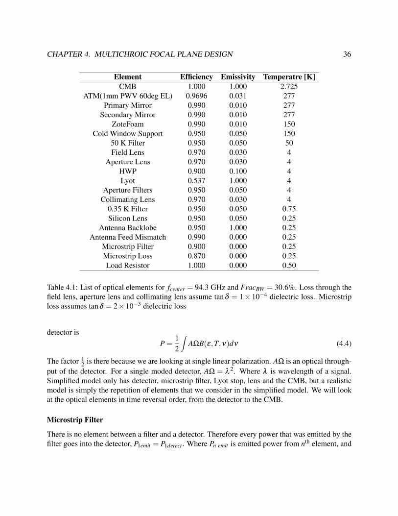
CHAPTER 4. MULTICHROIC FOCAL PLANE DESIGN 36
Element Efficiency Emissivity Temperatre [K]CMB 1.000 1.000 2.725
ATM(1mm PWV 60deg EL) 0.9696 0.031 277Primary Mirror 0.990 0.010 277
Secondary Mirror 0.990 0.010 277ZoteFoam 0.990 0.010 150
Cold Window Support 0.950 0.050 15050 K Filter 0.950 0.050 50Field Lens 0.970 0.030 4
Aperture Lens 0.970 0.030 4HWP 0.900 0.100 4Lyot 0.537 1.000 4
Aperture Filters 0.950 0.050 4Collimating Lens 0.970 0.030 4
0.35 K Filter 0.950 0.050 0.75Silicon Lens 0.950 0.050 0.25
Antenna Backlobe 0.950 1.000 0.25Antenna Feed Mismatch 0.990 0.000 0.25
Microstrip Filter 0.900 0.000 0.25Microstrip Loss 0.870 0.000 0.25Load Resistor 1.000 0.000 0.50
Table 4.1: List of optical elements for fcenter = 94.3 GHz and FracBW = 30.6%. Loss through thefield lens, aperture lens and collimating lens assume tanδ = 1× 10⁻⁴ dielectric loss. Microstriploss assumes tanδ = 2×10⁻³ dielectric loss
detector isP =
12
∫AΩB(ε,T,ν)dν (4.4)
The factor 12 is there because we are looking at single linear polarization. AΩ is an optical through-
put of the detector. For a single moded detector, AΩ = λ 2. Where λ is wavelength of a signal.Simplified model only has detector, microstrip filter, Lyot stop, lens and the CMB, but a realisticmodel is simply the repetition of elements that we consider in the simplified model. We will lookat the optical elements in time reversal order, from the detector to the CMB.
Microstrip Filter
There is no element between a filter and a detector. Therefore every power that was emitted by thefilter goes into the detector, P1emit = P1detect . Where Pn emit is emitted power from nth element, and
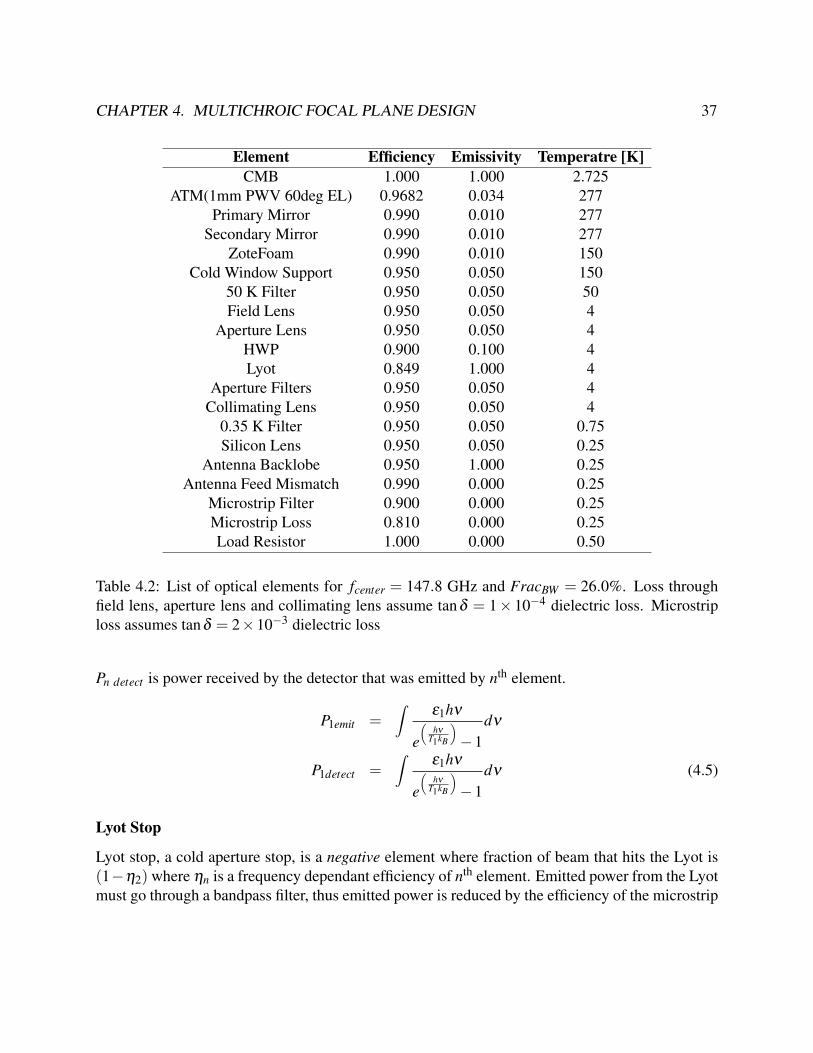
CHAPTER 4. MULTICHROIC FOCAL PLANE DESIGN 37
Element Efficiency Emissivity Temperatre [K]CMB 1.000 1.000 2.725
ATM(1mm PWV 60deg EL) 0.9682 0.034 277Primary Mirror 0.990 0.010 277
Secondary Mirror 0.990 0.010 277ZoteFoam 0.990 0.010 150
Cold Window Support 0.950 0.050 15050 K Filter 0.950 0.050 50Field Lens 0.950 0.050 4
Aperture Lens 0.950 0.050 4HWP 0.900 0.100 4Lyot 0.849 1.000 4
Aperture Filters 0.950 0.050 4Collimating Lens 0.950 0.050 4
0.35 K Filter 0.950 0.050 0.75Silicon Lens 0.950 0.050 0.25
Antenna Backlobe 0.950 1.000 0.25Antenna Feed Mismatch 0.990 0.000 0.25
Microstrip Filter 0.900 0.000 0.25Microstrip Loss 0.810 0.000 0.25Load Resistor 1.000 0.000 0.50
Table 4.2: List of optical elements for fcenter = 147.8 GHz and FracBW = 26.0%. Loss throughfield lens, aperture lens and collimating lens assume tanδ = 1× 10⁻⁴ dielectric loss. Microstriploss assumes tanδ = 2×10⁻³ dielectric loss
Pn detect is power received by the detector that was emitted by nth element.
P1emit =∫
ε1hν
e(
hν
T1kB
)−1
dν
P1detect =∫
ε1hν
e(
hν
T1kB
)−1
dν (4.5)
Lyot Stop
Lyot stop, a cold aperture stop, is a negative element where fraction of beam that hits the Lyot is(1−η2) where ηn is a frequency dependant efficiency of nth element. Emitted power from the Lyotmust go through a bandpass filter, thus emitted power is reduced by the efficiency of the microstrip

CHAPTER 4. MULTICHROIC FOCAL PLANE DESIGN 38
Figure 4.3: Simple model of a cryogenic receiver. Dark blue box represents a cold box with anaperture (Lyot stop). Green hemisphere represents a lenslet of a detector. Circular fan coming outfrom a lens represents detector beam. Arrows represent optical loading contributions from opticalelements.
filter η1.
P2emit =∫
ε2(1−η2)hν
e(
hν
T2kB
)−1
dν
P2detect =∫
η1ε2(1−η2)hν
e(
hν
T2kB
)−1
dν (4.6)
Lens
Example of lens can be repeated for other optical elements such as thermal filters and half-waveplate. Its emitted power is reduced by efficiencies of optical elements between the source and thedetector. For the simple case, efficiency is reduced at Lyot stop and microstrip filter.
P3emit =∫
ε3hν
e(
hν
T3kB
)−1
dν
P3detect =∫
η1η2ε3hν
e(
hν
T3kB
)−1
dν (4.7)
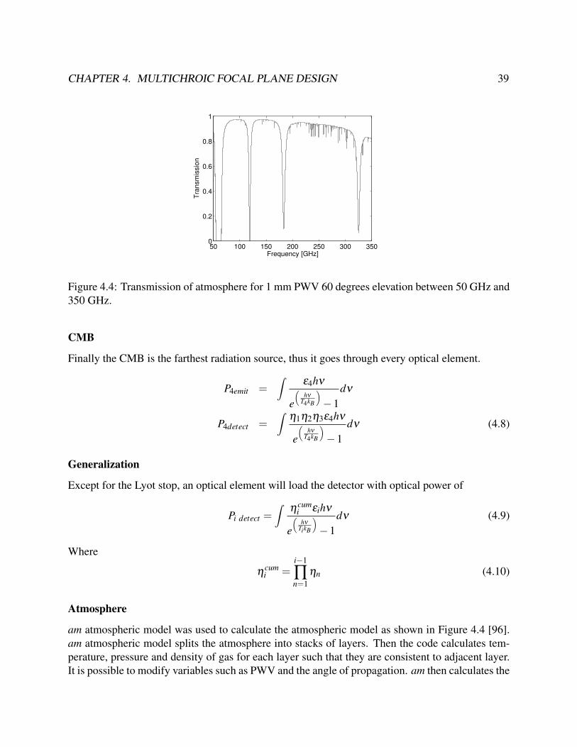
CHAPTER 4. MULTICHROIC FOCAL PLANE DESIGN 39
50 100 150 200 250 300 3500
0.2
0.4
0.6
0.8
1
Frequency [GHz]
Tra
nsm
issio
n
Figure 4.4: Transmission of atmosphere for 1 mm PWV 60 degrees elevation between 50 GHz and350 GHz.
CMB
Finally the CMB is the farthest radiation source, thus it goes through every optical element.
P4emit =∫
ε4hν
e(
hν
T4kB
)−1
dν
P4detect =∫
η1η2η3ε4hν
e(
hν
T4kB
)−1
dν (4.8)
Generalization
Except for the Lyot stop, an optical element will load the detector with optical power of
Pi detect =∫
ηcumi εihν
e(
hν
TikB
)−1
dν (4.9)
Where
ηcumi =
i−1
∏n=1
ηn (4.10)
Atmosphere
am atmospheric model was used to calculate the atmospheric model as shown in Figure 4.4 [96].am atmospheric model splits the atmosphere into stacks of layers. Then the code calculates tem-perature, pressure and density of gas for each layer such that they are consistent to adjacent layer.It is possible to modify variables such as PWV and the angle of propagation. am then calculates the
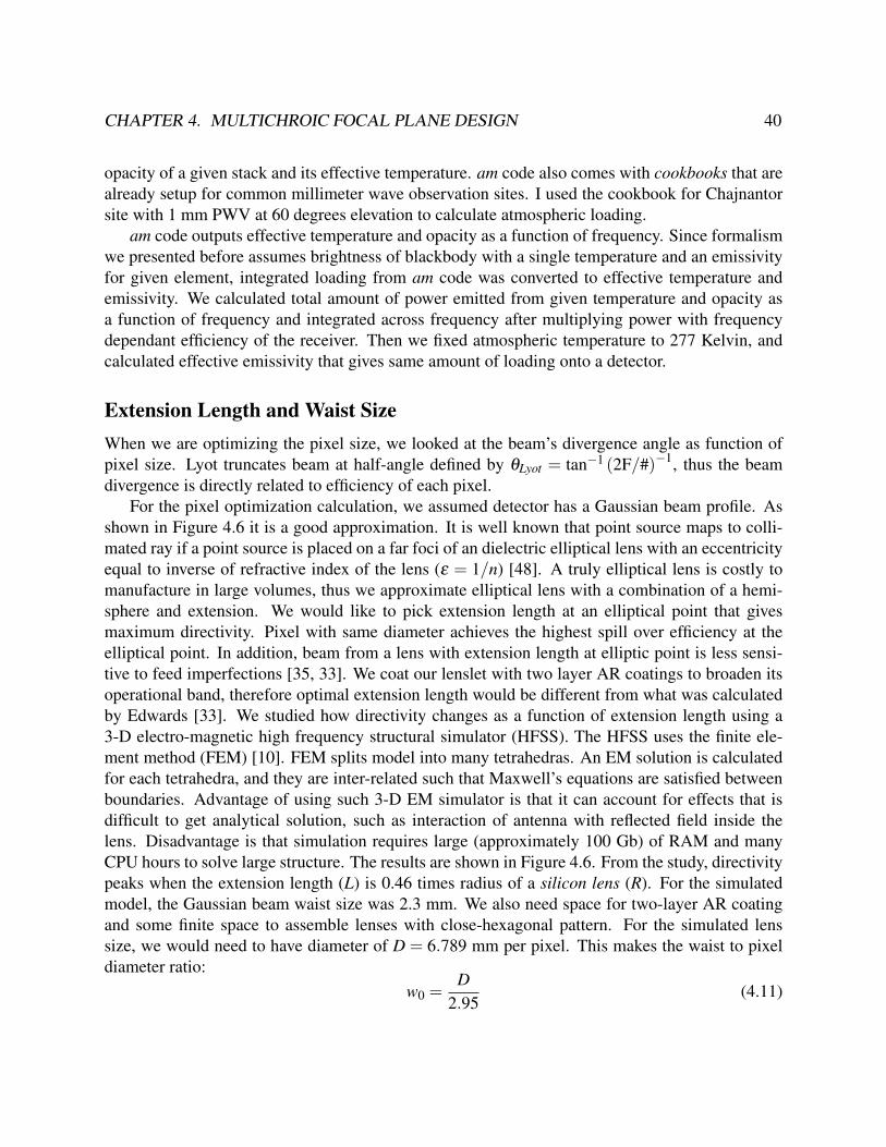
CHAPTER 4. MULTICHROIC FOCAL PLANE DESIGN 40
opacity of a given stack and its effective temperature. am code also comes with cookbooks that arealready setup for common millimeter wave observation sites. I used the cookbook for Chajnantorsite with 1 mm PWV at 60 degrees elevation to calculate atmospheric loading.
am code outputs effective temperature and opacity as a function of frequency. Since formalismwe presented before assumes brightness of blackbody with a single temperature and an emissivityfor given element, integrated loading from am code was converted to effective temperature andemissivity. We calculated total amount of power emitted from given temperature and opacity asa function of frequency and integrated across frequency after multiplying power with frequencydependant efficiency of the receiver. Then we fixed atmospheric temperature to 277 Kelvin, andcalculated effective emissivity that gives same amount of loading onto a detector.
Extension Length and Waist SizeWhen we are optimizing the pixel size, we looked at the beam’s divergence angle as function ofpixel size. Lyot truncates beam at half-angle defined by θLyot = tan−1 (2F/#)−1, thus the beamdivergence is directly related to efficiency of each pixel.
For the pixel optimization calculation, we assumed detector has a Gaussian beam profile. Asshown in Figure 4.6 it is a good approximation. It is well known that point source maps to colli-mated ray if a point source is placed on a far foci of an dielectric elliptical lens with an eccentricityequal to inverse of refractive index of the lens (ε = 1/n) [48]. A truly elliptical lens is costly tomanufacture in large volumes, thus we approximate elliptical lens with a combination of a hemi-sphere and extension. We would like to pick extension length at an elliptical point that givesmaximum directivity. Pixel with same diameter achieves the highest spill over efficiency at theelliptical point. In addition, beam from a lens with extension length at elliptic point is less sensi-tive to feed imperfections [35, 33]. We coat our lenslet with two layer AR coatings to broaden itsoperational band, therefore optimal extension length would be different from what was calculatedby Edwards [33]. We studied how directivity changes as a function of extension length using a3-D electro-magnetic high frequency structural simulator (HFSS). The HFSS uses the finite ele-ment method (FEM) [10]. FEM splits model into many tetrahedras. An EM solution is calculatedfor each tetrahedra, and they are inter-related such that Maxwell’s equations are satisfied betweenboundaries. Advantage of using such 3-D EM simulator is that it can account for effects that isdifficult to get analytical solution, such as interaction of antenna with reflected field inside thelens. Disadvantage is that simulation requires large (approximately 100 Gb) of RAM and manyCPU hours to solve large structure. The results are shown in Figure 4.6. From the study, directivitypeaks when the extension length (L) is 0.46 times radius of a silicon lens (R). For the simulatedmodel, the Gaussian beam waist size was 2.3 mm. We also need space for two-layer AR coatingand some finite space to assemble lenses with close-hexagonal pattern. For the simulated lenssize, we would need to have diameter of D = 6.789 mm per pixel. This makes the waist to pixeldiameter ratio:
w0 =D
2.95(4.11)
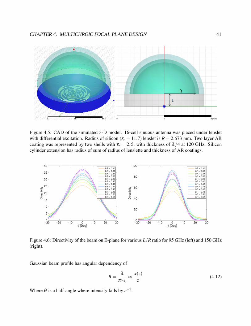
CHAPTER 4. MULTICHROIC FOCAL PLANE DESIGN 41
Figure 4.5: CAD of the simulated 3-D model. 16-cell sinuous antenna was placed under lensletwith differential excitation. Radius of silicon (εr = 11.7) lenslet is R = 2.673 mm. Two layer ARcoating was represented by two shells with εr = 2,5, with thickness of λ/4 at 120 GHz. Siliconcylinder extension has radius of sum of radius of lenslette and thickness of AR coatings.
−30 −20 −10 0 10 20 300
5
10
15
20
25
30
35
40
θ [Deg]
Directivity
L/R = 0.30
L/R = 0.32
L/R = 0.34
L/R = 0.36
L/R = 0.38
L/R = 0.40
L/R = 0.42
L/R = 0.44
L/R = 0.46
L/R = 0.48
L/R = 0.50
L/R = 0.52
−30 −20 −10 0 10 20 300
20
40
60
80
100
θ [Deg]
Directivity
L/R = 0.30
L/R = 0.32
L/R = 0.34
L/R = 0.36
L/R = 0.38
L/R = 0.40
L/R = 0.42
L/R = 0.44
L/R = 0.46
L/R = 0.48
L/R = 0.50
L/R = 0.52
Figure 4.6: Directivity of the beam on E-plane for various L/R ratio for 95 GHz (left) and 150 GHz(right).
Gaussian beam profile has angular dependency of
θ =λ
πw0≈ w(z)
z(4.12)
Where θ is a half-angle where intensity falls by e−2.

CHAPTER 4. MULTICHROIC FOCAL PLANE DESIGN 42
0.3 0.35 0.4 0.45 0.5600
650
700
750
800
850
900
950
L/R
Inte
gra
ted D
irectivity
0.3 0.35 0.4 0.45 0.51100
1200
1300
1400
1500
1600
1700
L/RIn
tegra
ted D
irectivity
Figure 4.7: Integrated directivity for 95 GHz (left) and 150 GHz (right). Directivity was integrateddown to the angle defined by F/#.
0.3 0.35 0.4 0.45 0.52
2.05
2.1
2.15
2.2
2.25
2.3
2.35
2.4
L/R
Wais
t [m
m]
0.3 0.35 0.4 0.45 0.51.9
2
2.1
2.2
2.3
2.4
2.5
L/R
Wais
t [m
m]
Figure 4.8: Gaussian beam waist size for simulated beam for 95 GHz (left) 150 GHz (right)
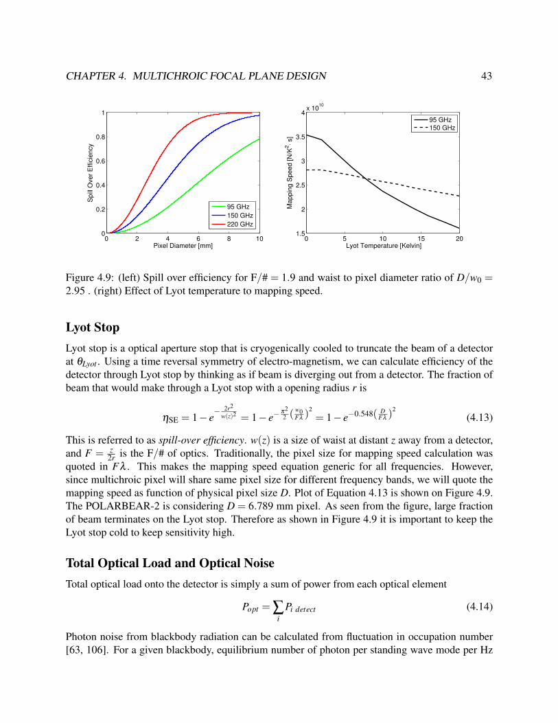
CHAPTER 4. MULTICHROIC FOCAL PLANE DESIGN 43
0 2 4 6 8 100
0.2
0.4
0.6
0.8
1
Pixel Diameter [mm]
Spill
Over
Effic
iency
95 GHz
150 GHz
220 GHz
0 5 10 15 201.5
2
2.5
3
3.5
4x 10
10
Lyot Temperature [Kelvin]
Mappin
g S
peed [N
/K2⋅ s
]
95 GHz
150 GHz
Figure 4.9: (left) Spill over efficiency for F/# = 1.9 and waist to pixel diameter ratio of D/w0 =2.95 . (right) Effect of Lyot temperature to mapping speed.
Lyot StopLyot stop is a optical aperture stop that is cryogenically cooled to truncate the beam of a detectorat θLyot . Using a time reversal symmetry of electro-magnetism, we can calculate efficiency of thedetector through Lyot stop by thinking as if beam is diverging out from a detector. The fraction ofbeam that would make through a Lyot stop with a opening radius r is
ηSE = 1− e− 2r2
w(z)2 = 1− e−π22 (
w0Fλ)
2
= 1− e−0.548( DFλ)
2
(4.13)
This is referred to as spill-over efficiency. w(z) is a size of waist at distant z away from a detector,and F = z
2r is the F/# of optics. Traditionally, the pixel size for mapping speed calculation wasquoted in Fλ . This makes the mapping speed equation generic for all frequencies. However,since multichroic pixel will share same pixel size for different frequency bands, we will quote themapping speed as function of physical pixel size D. Plot of Equation 4.13 is shown on Figure 4.9.The POLARBEAR-2 is considering D = 6.789 mm pixel. As seen from the figure, large fractionof beam terminates on the Lyot stop. Therefore as shown in Figure 4.9 it is important to keep theLyot stop cold to keep sensitivity high.
Total Optical Load and Optical NoiseTotal optical load onto the detector is simply a sum of power from each optical element
Popt = ∑i
Pi detect (4.14)
Photon noise from blackbody radiation can be calculated from fluctuation in occupation number[63, 106]. For a given blackbody, equilibrium number of photon per standing wave mode per Hz
CHAPTER 4. MULTICHROIC FOCAL PLANE DESIGN 44
of bandwidth per second is given by
n =1
ehν
T kB −1(4.15)
Then fluctuation in photon arrival for such blackbody is
〈(∆n)2〉= n+n2 (4.16)
We refer to such fluctuations in occupation number as photon noise. Noise equivalent power (NEP)is a signal power that will give signal-to-noise ratio of 1 for 1 Hz of bandwidth. It is defined as
NEPγ =
√2∫
popthνdν +∫
p2optdν (4.17)
Where popt is the power spectal density associated with Popt . γ refers to the fact this is a noise dueto photon contribution. Because of
∫p2
optdν term, NEP must be calculated using spectral densityfrom Poptl instead of calculating NEP from individual Pi and add them in quadrature.
4.4 Bolometer Design and Thermal Carrier Noise
IntroductionThe bolometer was invented by Langley [70]. The bolometer is a type of detector that detectsincident electromagnetic radiation by converting radiation to heat and read change in electricalresistance of temperature dependant material. In its simplest form, a bolometer has a thermallyisolated island that is connected to a thermal bath with temperature Tb via a weak link with thermalconductance G. Isolated island contains an absorber that receives optical signal and a thermister,temperature dependant resistor. A thermistor is either voltage biased or current biased. The isolatedisland thus receives optical power and electrical power. At steady state, temperature of isolatedisland T would be
P = Popt +Pelec = G(T −Tb) (4.18)
Where P is a total power on an island. Dynamic heat conductance g is defined as
g =∂P∂T
(4.19)
Suppose P changes to a new value P′ instantaneously, then bolometer island reaches to differenttemperature T ′ = Tb +
P′G with a time constant
τ0 =Cg
(4.20)
Previous generation bolometers were made with carbon resistor and doped semiconductors as ther-misters [22, 43]. These thermisters have steep increases in resistance as a function of decreasing
CHAPTER 4. MULTICHROIC FOCAL PLANE DESIGN 45
temperature, and their high impedance and negative dRdT preferred current biasing for stable oper-
ation. The bolometer behaves as an ideal linear detector with high sensitivity as the steepness ofa transition increases. The superconducting transition of a superconductor metal has very sharpdRdT curve. Superconducting thermister’s low impedance and positive dR
dT prefers thermister to bevoltage biased for stable operation [56]. Voltage biased detector has an advantage that current canbe amplified by superconducting quantum interference device (SQUID) at cryogenic temperaturefor to achieve low noise performance. Multiplexing is also easier with voltage biased detectors.Review for superconducting TES bolometer was done by Irwin and Hilton [57]. Detailed calcula-tion of bolometer’s response including parasitics in readout were also given in the review. Whilethe complete calculation is useful, we’ll first introduce simple calculation to get more intuitiveunderstanding [106, 73, 40]. We’ll introduce results from complete derivation when discussingstability criteria.
Basic OperationElectrical bias power applied to a bolometer with voltage bias is
Pelec =V 2
elecR
(4.21)
When temperature of a bolometer island tries to change as optical power changes, temperature ofthe bolometer island is stabilized by negative feed back.
dPelec
dT=−
V 2elecR2
dRdT
=−Pelecα
Tc(4.22)
Where α is logarithmic slope of superconducting transition α = ∂ logR∂ logT = T
R∂R∂T . Negative feed back
allows operation point of bolometer to be locked onto a sharp transition of a superconductor attransition temperature Tc. Suppose small change in optical power δPopteiωt changed temperatureof an bolometer island by δTeiωt . We can write down energy conservation of bolometer system as
P+δPopteiωt− Pelecα
TcδTeiωt = G(Tc−Tb)+(g+ iωC)δTeiωt (4.23)
Time varying part of is
δPopt =
(Pelecα
Tc+g+ iωC
)δT (4.24)
We can view this as amplifier with output δP = δPopt + δPelec = (g+ iωC)δT and feedback
δPelec =−(
Pelecα
Tc
)δT . We can define loop gain of such amplifying circuit as
L (ω) =−δPelec
δP=
Pelecα
gTc(1+ iωτ0)=
L
1+ iωτ0(4.25)
CHAPTER 4. MULTICHROIC FOCAL PLANE DESIGN 46
Where L = Pbα
gTcis DC the loop gain. Responsivity SI =
dIelecdPopt
is
SI =dIelec
dPopt(4.26)
=1
Velec
dPelec
dPopt(4.27)
=1
Velec
−(
Pelecα
Tc
)δT(
Pelecα
Tc+g+ iωC
)δT
(4.28)
= − 1Velec
L
L +11
1+ iωτ(4.29)
Where time constant τ isτ =
τ0
L +1(4.30)
Thus bolometer’s effective time constant is decreased as loop gain goes up. For a high loop gainamplifier L 1, responsivity reduces to
SI =−1
Velec(4.31)
Just like electrical amplifier circuit, high loop gain of negative feedback allows responsivity ofbolometer to be independent of bolometer’s intrinsic characteristics. This helps array of bolometersto have uniform performance [57].
Thermal Carrier NoiseNoise equivalent power that arises from fluctuation in thermal flow through weak link between twodifferent temperature is given by Mather [81].
NEPg =√
4γkBT 2c g (4.32)
Where γ is a numerical factor γ = n+12n+3
1−(Tb/Tc)2n+3
1−(Tb/Tc)n+1 . n is an index for thermal conductivity wheren = 1 for electron based conduction and n = 3 for phonon heat transfer.
To start the optimization process, we first decide the geometry of the weak link by choosingthe best saturated power, Psat . We define Psat as a power that flows through weak link betweenbolometer island at Tc and thermal bath at Tb. We want to pick Psat to be factor of few times greaterthan expected Popt we calculated from optical load calculation. This allows Pelec to be able toprovide enough feedback for stable operation, and it gives extra buffer for increased Popt duringnon-optimal weather. However, we do not want to increase Psat unnecessarily since increasing Psatwill increase NEPg. The POLARBEAR-2 bolometers were designed with Psat = 2.5Popt . Powerflowing though bolometer legs can be calculated from a model Psat = NAk(T )dT
dx . Where A is
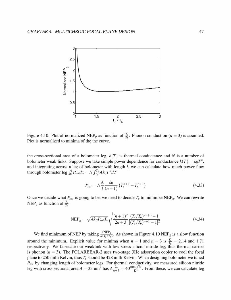
CHAPTER 4. MULTICHROIC FOCAL PLANE DESIGN 47
1 1.5 2 2.5 30
0.5
1
1.5
2
2.5
3
Tc / T
b
Norm
aliz
ed N
EP
g
Figure 4.10: Plot of normalized NEPg as function of TcTb
. Phonon conduction (n = 3) is assumed.Plot is normalized to minima of the the curve.
the cross-sectional area of a bolometer leg, k(T ) is thermal conductance and N is a number ofbolometer weak links. Suppose we take simple power dependence for conductance k(T ) = k0T n,and integrating across a leg of bolometer with length l, we can calculate how much power flowthrough bolometer leg
∫ l0 Psatdx = N
∫ TbTc
Ak0T ndT
Psat = NAl
k0
(n+1)(T n+1
c −T n+1b
)(4.33)
Once we decide what Psat is going to be, we need to decide Tc to minimize NEPg. We can rewriteNEPg as function of Tc
Tb
NEPg =√
4kBPsatTb
√(n+1)2
2n+3(Tc/Tb)2n+3−1[(Tc/Tb)n+1−1]2
(4.34)
We find minimum of NEP by taking dNEPgd(Tc/Tb)
. As shown in Figure 4.10 NEPg is a slow function
around the minimum. Explicit value for minima when n = 1 and n = 3 is TcTb
= 2.14 and 1.71respectively. We fabricate our weaklink with low stress silicon nitride leg, thus thermal carrieris phonon (n = 3). The POLARBEAR-2 uses two-stage 3He adsorption cooler to cool the focalplane to 250 milli Kelvin, thus Tc should be 428 milli Kelvin. When designing bolometer we tunedPsat by changing length of bolometer legs. For thermal conductivity, we measured silicon nitrideleg with cross sectional area A = 33 um2 has A k0
n+1 = 40mm·pWK4 . From these, we can calculate leg
CHAPTER 4. MULTICHROIC FOCAL PLANE DESIGN 48
length to be
l = NA
Psat
k0
(n+1)(T n+1
c −T n+1b
)(4.35)
Once Psat is set, we can calculate G and g by
G =Psat
Tc−Tb= N
Al
k0
(n+1)T n+1
c −T n+1b
Tc−Tb(4.36)
and
g =∂Psat
∂Tc= N
Al
k0T nc (4.37)
Once g get calculated, NEPg can be calculated with Equation 4.32.
4.5 Readout NoiseBefore we decide on the resistance of the TES at the operation point (RT ES) and inductance forreadout (L), read-out noise needs to be considered. For the POLARBEAR-2, we followed noisecontribution calculated for the POLARBEAR-1 [15, 60]. There were contributions from bolometernoise and demodulator noise. Bolometer noise includs contributions from SQUID noise, noiseon SQUID controller board and Johnson noise from various resistors used in the readout chain.Demodulator noise included amplifier noise and digitation noise. Expected readout noise referredto input coil of a SQUID was 7 pA√
Hz. The POLARBEAR-1 measured 9 pA√
Hz. For the POLARBEAR-
2 calculations, we used NEIread = 7 pA√Hz
.
4.6 Readout ParametersSince we decided Psat = 2.5Popt , Pelec = 1.5Popt . We can convert NEIread to NEPread with respon-sivity at high loop gain 1
Velec, such that NEPread =VelecNEIread. Suppose we want to keep total noise
increase due to readout noise contribution to be less than 10%
NEPmaxread =
√((1.1)2−1)(NEP2
γ +NEP2g) (4.38)
This constraints maximum V maxelec .
V maxelec = NEPmax
read/NEIread (4.39)
Since Pelec =V 2
elecRT ES
we can calculate RmaxT ES
RmaxT ES =
V 2elec
Pelec(4.40)
CHAPTER 4. MULTICHROIC FOCAL PLANE DESIGN 49
From the point view of minimizing the non-ideal effect from parasitic resistance, we want to max-imize Rmax
T ES. Typical fluctuation in RT ES across wafer is ±15% that predominantly arises fromdifferent etch rate of aluminium during wet-etch process. We can then set RT ES = Rmax
T ES/1.15 andRmin
T ES = RT ES×0.85. One component of such a stray resistance is the dielectric loss in a capacitorused to make LCR circuit. We developed super conducting interdigitated capacitor on high resis-tivity silicon to minimize ohmic loss and dielectric loss at capacitor. Discussion of interdigitatedcapacitor is given in Section 5.13. We can describe such loss as an equivalent series resistance(ESR). The ESR is related to tan(δ ) of material and inductance of LCR circuit by
RESR = 2π f L tan(δ ) (4.41)
We used single crystal float-zone silicon with 10 K Ω− cm resistivity. tan(δ ) for similar siliconwas tan(δ ) = 2×10⁻⁴ at 10 Kelvin (6.8 GHz) [65]. To keep a stable read-out, we want to minimizeRESR. We set a requirement that RESR should be less than 20% of Rmin
T ES. Next we decided on thefrequency range of the read-out. We do not want to use very high frequency as this will make thestray inductance requirement more stringent. The benefit of having high frequency is that read-out would use smaller fractional bandwidth and we can use smaller interdigitated capacitors andinductors. Smaller capacitor and inductor would facilitate fabricating effort. We first calculate thelargest capacitor that we can fabricate. Then we decided on fmin. We can then calculate fmax frommux factor and ∆ f that would satisfy cross-talk requirement. Once we decide on f max we canchose to calculate the maximum allowable Lmax by
Lmax =0.2Rmin
T ES2π f max tan(δ )
(4.42)
Lmax will be different for two different frequency bands. For an experiment, it is advantageous touse same inductor value to facilitate fabrication effort. Smaller L value between two frequencybands should be used to clear ESR requirement. Frequency spacing ∆ f should be set to meetcross-talk requirement. Cross-talk (CT) between channels is
CT =
(Rmax
T ES +RESR
4π∆ f Lmax
)2
(4.43)
We set cross-talk requirement by requiring that only acceptable level of the CMB tempeatureanisotropy signal to leak into B-mode polarization spectrum. Such effect get reduced further bysky rotation. We set readout cross-talk requirement to 1%. We find ∆ f by
∆ f >Rmax
T ES +RESR
0.4π∆ f Lmax (4.44)
chosing The bigger RT ES between two frequency bands should be used for the calculation. Wethen vary frequency spacing with expected accuracy of inductors and capacitor components. Mea-surement of how accurate we can fabricate inductors and capacitors are on going. We assumed wecan fabricate reactive components to 0.5% fractional accuracy. Since many component variablesdepend on each other, these steps were iterated few times until ∆ f and L converged.
CHAPTER 4. MULTICHROIC FOCAL PLANE DESIGN 50
Time ConstantsTime constant τ of bolometer is tuned by changing heat capacity of bolometer island C. There aretwo bounding requirements for the time constant. If τ is too large, telescope needs to be scannedat a slower speed, thus large angular scale data will be affacted by 1
f noise. If τ is too short,the detector bandwidth exceeds the readout bandwidth and the detector becomes unstable. Wewill discuss two bounding requirements, and we will show our design allow bolometer to operatebetween two bounding requirements.
Scan Speed
To set an upper limit on τ , we considered telescope scan speed and beam size. The HTT is designedto scan in azimuth direction at 4 degrees per second. The lowest elevation the POLARBEAR-2is planning to observe is 30 degrees. Thus the fastest scan speed on sky would be 4 [deg/sec]×cos(30) = 3.47 [deg/sec]. Beam size for a pixel diameter can be calculated with the Fraunhofer’sdiffraction relation [21].
ψ(θ) =∫ R
0
∫ 2π
0ψa(r)e−ik sin(θ)cos(φ)rdrdφ (4.45)
Where ψa(r) is electric field on aperture, and R is outer radius of an aperture. Suppose we calculatethis on primary mirror of the HTT. We assumed beam get truncated hard at R = 1.25 meters. Weassume a truncated Gaussian beam is formed on primary mirror from detector (time reverse sense)
ψa(r) = e−(
r2F/#R tan(λ/πw)
)2
, r ≤ Rψa(r) = 0 , r > R (4.46)
Calculated value for 95 GHz and 150 GHz beam is plotted in Figure 4.11. It is necessary to samplesky faster than Nyquest frequency. Suppose the safety factor is 4, we need to take data at
τbeam =1
4[deg/sec]θFWHM
2×4(4.47)
Readout Time Constants Requirement
The lower end of time constant constraint comes from a readout requirement. We first writedown the thermal differential equation and electrical differential equation of a voltage biased TESbolometer [57],
CdTdt
+G(Tc−Tb) = Popt +Pelec
V = LdIdt
+ IRL + IRT ES (4.48)
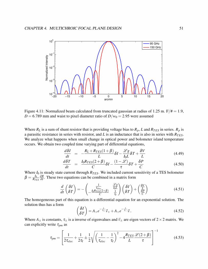
CHAPTER 4. MULTICHROIC FOCAL PLANE DESIGN 51
−20 −15 −10 −5 0 5 10 15 2010
−4
10−3
10−2
10−1
100
arcmin
Norm
aliz
ed Inte
nsity
95 GHz
150 GHz
Figure 4.11: Normalized beam calculated from truncated gaussian at radius of 1.25 m. F/# = 1.9,D = 6.789 mm and waist to pixel diameter ratio of D/w0 = 2.95 were assumed
Where RL is a sum of shunt resistor that is providing voltage bias to Rp, L and RT ES in series. Rp isa parasitic resistance in series with resistor, and L is an inductance that is also in series with RT ES.We analyze what happens when small change in optical power and bolometer island temperatureoccurs. We obtain two coupled time varying part of differential equations,
dδ Idt
= −RL +RT ES(1+β )
Lδ I−L g
I0LδT +
δVL
(4.49)
dδTdt
=I0RT ES(2+β )
Cδ I− (1−L )
τδT +
δPC
(4.50)
Where I0 is steady state current through RT ES. We included current sensitivity of a TES bolometerβ = I0
RT ES
∂R∂ I . These two equations can be combined in a matrix form
ddt
(δ IδT
)=−
(1
τelec
L gI0L
− I0RT ES(2+β )C
1τI
)(δ IδT
)+
(δVL
δPC
)(4.51)
The homogeneous part of this equation is a differential equation for an exponential solution. Thesolution thus has a form (
δ IδT
)= A+e−
tτ+~v++A+e−
tτ−~v− (4.52)
Where A± is constants, τ± is a inverse of eigenvalues and~v± are eigen vectors of 2×2 matrix. Wecan explicitly write τpm as
τpm =
12τelec
+1
2τI± 1
2
√(1
τelec− 1
τI
)2
−4RT ES
LL (2+β )
τ
−1
(4.53)
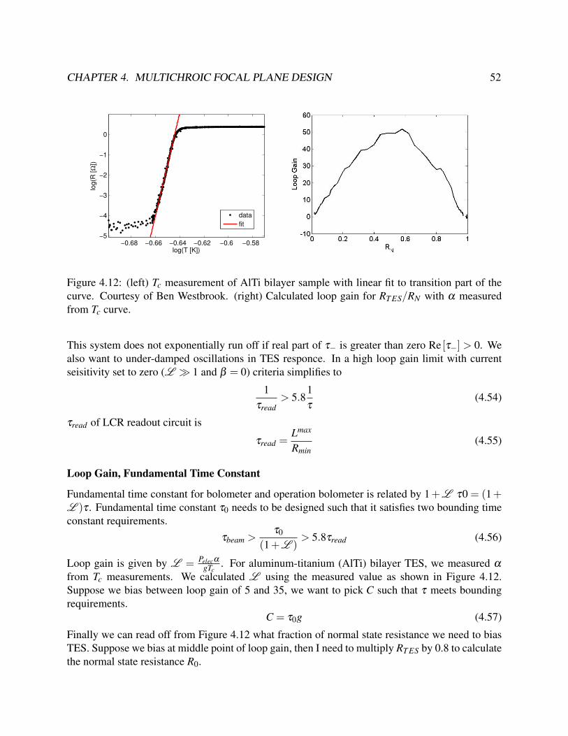
CHAPTER 4. MULTICHROIC FOCAL PLANE DESIGN 52
−0.68 −0.66 −0.64 −0.62 −0.6 −0.58−5
−4
−3
−2
−1
0
log(T [K])
log(R
[Ω
])
data
fit
Figure 4.12: (left) Tc measurement of AlTi bilayer sample with linear fit to transition part of thecurve. Courtesy of Ben Westbrook. (right) Calculated loop gain for RT ES/RN with α measuredfrom Tc curve.
This system does not exponentially run off if real part of τ− is greater than zero Re [τ−] > 0. Wealso want to under-damped oscillations in TES responce. In a high loop gain limit with currentseisitivity set to zero (L 1 and β = 0) criteria simplifies to
1τread
> 5.81τ
(4.54)
τread of LCR readout circuit is
τread =Lmax
Rmin(4.55)
Loop Gain, Fundamental Time Constant
Fundamental time constant for bolometer and operation bolometer is related by 1+L τ0 = (1+L )τ . Fundamental time constant τ0 needs to be designed such that it satisfies two bounding timeconstant requirements.
τbeam >τ0
(1+L )> 5.8τread (4.56)
Loop gain is given by L = Pelecα
gTc. For aluminum-titanium (AlTi) bilayer TES, we measured α
from Tc measurements. We calculated L using the measured value as shown in Figure 4.12.Suppose we bias between loop gain of 5 and 35, we want to pick C such that τ meets boundingrequirements.
C = τ0g (4.57)
Finally we can read off from Figure 4.12 what fraction of normal state resistance we need to biasTES. Suppose we bias at middle point of loop gain, then I need to multiply RT ES by 0.8 to calculatethe normal state resistance R0.
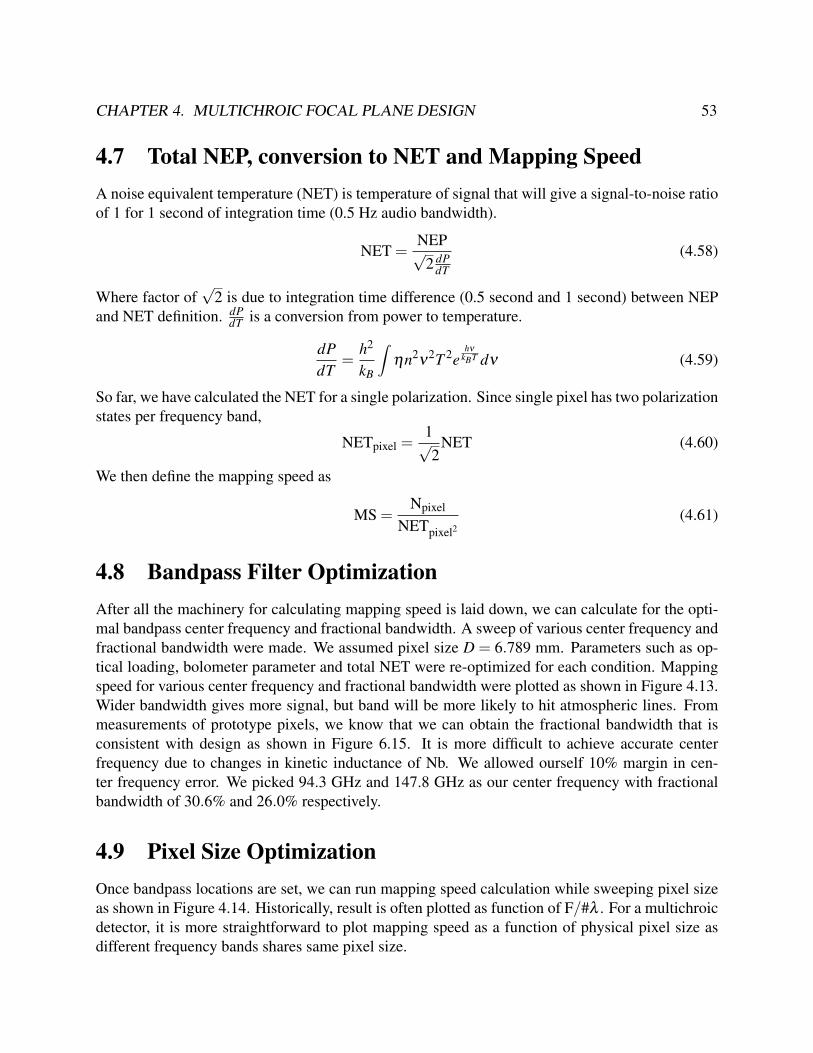
CHAPTER 4. MULTICHROIC FOCAL PLANE DESIGN 53
4.7 Total NEP, conversion to NET and Mapping SpeedA noise equivalent temperature (NET) is temperature of signal that will give a signal-to-noise ratioof 1 for 1 second of integration time (0.5 Hz audio bandwidth).
NET =NEP√
2 dPdT
(4.58)
Where factor of√
2 is due to integration time difference (0.5 second and 1 second) between NEPand NET definition. dP
dT is a conversion from power to temperature.
dPdT
=h2
kB
∫ηn2
ν2T 2e
hν
kBT dν (4.59)
So far, we have calculated the NET for a single polarization. Since single pixel has two polarizationstates per frequency band,
NETpixel =1√2
NET (4.60)
We then define the mapping speed as
MS =Npixel
NETpixel2(4.61)
4.8 Bandpass Filter OptimizationAfter all the machinery for calculating mapping speed is laid down, we can calculate for the opti-mal bandpass center frequency and fractional bandwidth. A sweep of various center frequency andfractional bandwidth were made. We assumed pixel size D = 6.789 mm. Parameters such as op-tical loading, bolometer parameter and total NET were re-optimized for each condition. Mappingspeed for various center frequency and fractional bandwidth were plotted as shown in Figure 4.13.Wider bandwidth gives more signal, but band will be more likely to hit atmospheric lines. Frommeasurements of prototype pixels, we know that we can obtain the fractional bandwidth that isconsistent with design as shown in Figure 6.15. It is more difficult to achieve accurate centerfrequency due to changes in kinetic inductance of Nb. We allowed ourself 10% margin in cen-ter frequency error. We picked 94.3 GHz and 147.8 GHz as our center frequency with fractionalbandwidth of 30.6% and 26.0% respectively.
4.9 Pixel Size OptimizationOnce bandpass locations are set, we can run mapping speed calculation while sweeping pixel sizeas shown in Figure 4.14. Historically, result is often plotted as function of F/#λ . For a multichroicdetector, it is more straightforward to plot mapping speed as a function of physical pixel size asdifferent frequency bands shares same pixel size.
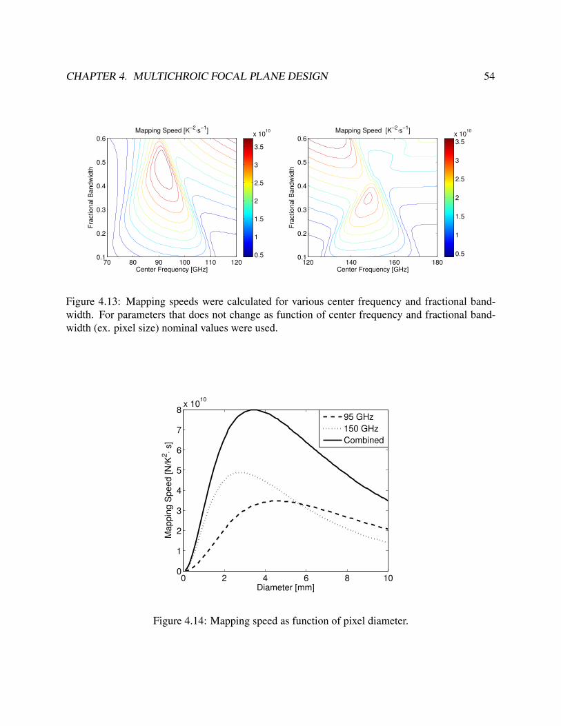
CHAPTER 4. MULTICHROIC FOCAL PLANE DESIGN 54
Center Frequency [GHz]
Fra
ctional B
andw
idth
Mapping Speed [K−2
⋅s−1
]
70 80 90 100 110 1200.1
0.2
0.3
0.4
0.5
0.6
0.5
1
1.5
2
2.5
3
3.5
x 1010
Center Frequency [GHz]
Fra
ctional B
andw
idth
Mapping Speed [K−2
⋅s−1
]
120 140 160 1800.1
0.2
0.3
0.4
0.5
0.6
0.5
1
1.5
2
2.5
3
3.5x 10
10
Figure 4.13: Mapping speeds were calculated for various center frequency and fractional band-width. For parameters that does not change as function of center frequency and fractional band-width (ex. pixel size) nominal values were used.
0 2 4 6 8 100
1
2
3
4
5
6
7
8x 10
10
Diameter [mm]
Mappin
g S
peed [N
/K2⋅ s
]
95 GHz
150 GHz
Combined
Figure 4.14: Mapping speed as function of pixel diameter.
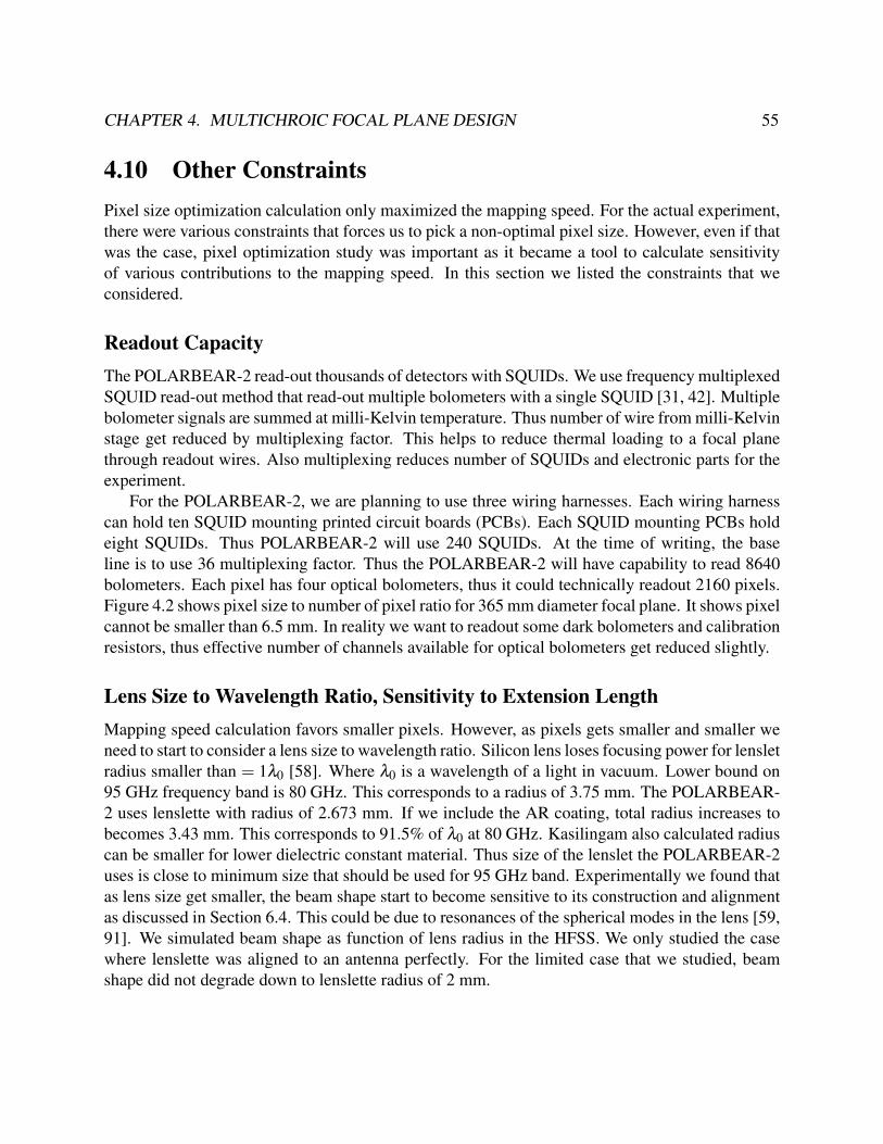
CHAPTER 4. MULTICHROIC FOCAL PLANE DESIGN 55
4.10 Other ConstraintsPixel size optimization calculation only maximized the mapping speed. For the actual experiment,there were various constraints that forces us to pick a non-optimal pixel size. However, even if thatwas the case, pixel optimization study was important as it became a tool to calculate sensitivityof various contributions to the mapping speed. In this section we listed the constraints that weconsidered.
Readout CapacityThe POLARBEAR-2 read-out thousands of detectors with SQUIDs. We use frequency multiplexedSQUID read-out method that read-out multiple bolometers with a single SQUID [31, 42]. Multiplebolometer signals are summed at milli-Kelvin temperature. Thus number of wire from milli-Kelvinstage get reduced by multiplexing factor. This helps to reduce thermal loading to a focal planethrough readout wires. Also multiplexing reduces number of SQUIDs and electronic parts for theexperiment.
For the POLARBEAR-2, we are planning to use three wiring harnesses. Each wiring harnesscan hold ten SQUID mounting printed circuit boards (PCBs). Each SQUID mounting PCBs holdeight SQUIDs. Thus POLARBEAR-2 will use 240 SQUIDs. At the time of writing, the baseline is to use 36 multiplexing factor. Thus the POLARBEAR-2 will have capability to read 8640bolometers. Each pixel has four optical bolometers, thus it could technically readout 2160 pixels.Figure 4.2 shows pixel size to number of pixel ratio for 365 mm diameter focal plane. It shows pixelcannot be smaller than 6.5 mm. In reality we want to readout some dark bolometers and calibrationresistors, thus effective number of channels available for optical bolometers get reduced slightly.
Lens Size to Wavelength Ratio, Sensitivity to Extension LengthMapping speed calculation favors smaller pixels. However, as pixels gets smaller and smaller weneed to start to consider a lens size to wavelength ratio. Silicon lens loses focusing power for lensletradius smaller than = 1λ0 [58]. Where λ0 is a wavelength of a light in vacuum. Lower bound on95 GHz frequency band is 80 GHz. This corresponds to a radius of 3.75 mm. The POLARBEAR-2 uses lenslette with radius of 2.673 mm. If we include the AR coating, total radius increases tobecomes 3.43 mm. This corresponds to 91.5% of λ0 at 80 GHz. Kasilingam also calculated radiuscan be smaller for lower dielectric constant material. Thus size of the lenslet the POLARBEAR-2uses is close to minimum size that should be used for 95 GHz band. Experimentally we found thatas lens size get smaller, the beam shape start to become sensitive to its construction and alignmentas discussed in Section 6.4. This could be due to resonances of the spherical modes in the lens [59,91]. We simulated beam shape as function of lens radius in the HFSS. We only studied the casewhere lenslette was aligned to an antenna perfectly. For the limited case that we studied, beamshape did not degrade down to lenslette radius of 2 mm.
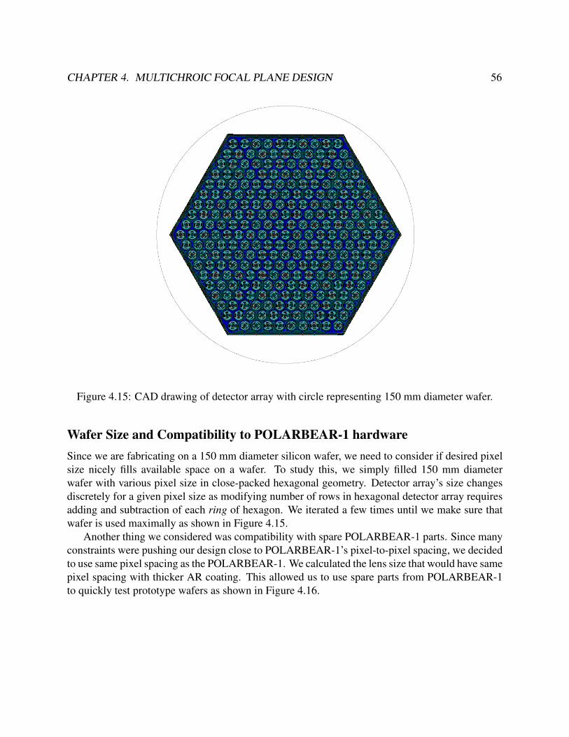
CHAPTER 4. MULTICHROIC FOCAL PLANE DESIGN 56
Figure 4.15: CAD drawing of detector array with circle representing 150 mm diameter wafer.
Wafer Size and Compatibility to POLARBEAR-1 hardwareSince we are fabricating on a 150 mm diameter silicon wafer, we need to consider if desired pixelsize nicely fills available space on a wafer. To study this, we simply filled 150 mm diameterwafer with various pixel size in close-packed hexagonal geometry. Detector array’s size changesdiscretely for a given pixel size as modifying number of rows in hexagonal detector array requiresadding and subtraction of each ring of hexagon. We iterated a few times until we make sure thatwafer is used maximally as shown in Figure 4.15.
Another thing we considered was compatibility with spare POLARBEAR-1 parts. Since manyconstraints were pushing our design close to POLARBEAR-1’s pixel-to-pixel spacing, we decidedto use same pixel spacing as the POLARBEAR-1. We calculated the lens size that would have samepixel spacing with thicker AR coating. This allowed us to use spare parts from POLARBEAR-1to quickly test prototype wafers as shown in Figure 4.16.
CHAPTER 4. MULTICHROIC FOCAL PLANE DESIGN 57
Figure 4.16: (left) Photograph of sinuous array in POLARBEAR-1 spare invar holder. (right)POLARBEAR-1 spare lenslet array was used for testing
4.11 SensitivityWe decided the POLARBEAR-2 would have a pixel to pixel spacing of 6.789 mm. 271 pixels fills150mm wafer. This summed up to 7,588 optically active bolometers. Our read-out has capabilityto read 8640 bolometers, so it also worked well with upper limit of readout capability. Extrachannels allowed us to wire up bolometers that are not connected to antenna, dark bolometers, tobe readout as a check against direct stimulation on bolometers. Also a pixel spacing that is sameas the POLARBEAR-1 allowed some initial tests by using POLARBEAR-1 spare parts.
SensitivityWe can translate this to a sensitivity to the CMB B-mode
∆CBBl =
√2
(2l +1) fsky
[CBB
l +w−1P W−1
l
](4.62)
Where fsky is fraction of full-sky the POLARBEAR-2 planning to observe. Weight factor w−1P is
given by
w−1P =
4π fsky
t1
MS(4.63)
and assuming Gaussian illumination on primary mirror, window function W−1l is
W−1l = el(l+1)σ2
(4.64)
Where σ is spread in Gaussian beam profile 12πσ2 e−θ 2/2σ2
[129]. For time t, we multiplied plannedobservation of 3 years with conservative estimate of efficiencies. Observation efficiency is sum-marized in Table 4.6

CHAPTER 4. MULTICHROIC FOCAL PLANE DESIGN 58
95 GHz 150 GHzF/# 1.9
Lenslette size 5.346 mmAR coating 0.72 mmLR Ratio 0.46
fcenter 94.3 GHz 147.8 GHzfBW 30.6 % 26.0 %
Optical efficiency 22.5 % 31.8 %Popt 2.9 pW 4.9 pWPsat 7.2 pW 12.2 pW
fPelec/Popt 1.5Tc 428 mK 428 mKTb 250 mK 250 mKG 40.7 pW/K 69.1 pW/Kg 76.4 pW/K 129.6 pW/KC 0.76 pJ/K 1.30 pJ/K
RT ES 0.89 1.13fRN 0.6R0 1.48 1.89α 250L 40τ 0.25 msτ0 10 ms
Table 4.3: Detector parameters
4.12 Summary of PB-2 Focal Plane ParametersSummary of focal plane parameters for the POLARBEAR-2 experiment are listed on Table 4.5.Detector parameters are listed on Table 4.3. Readout parameters are listed on Table 4.4. Noiseestimate and sensitivity prediction for the POLARBEAR-2 experiment is summarized on Table 4.7.
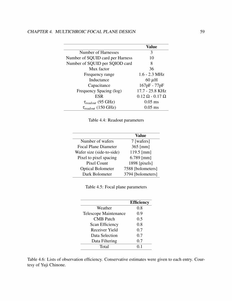
CHAPTER 4. MULTICHROIC FOCAL PLANE DESIGN 59
ValueNumber of Harnesses 3
Number of SQUID card per Harness 10Number of SQUID per SQIOD card 8
Mux factor 36Frequency range 1.6 - 2.3 MHz
Inductance 60 µHCapacitance 167pF - 77pF
Frequency Spacing (log) 17.7 - 25.8 KHzESR 0.12 Ω - 0.17 Ω
τreadout (95 GHz) 0.05 msτreadout (150 GHz) 0.05 ms
Table 4.4: Readout parameters
ValueNumber of wafers 7 [wafers]
Focal Plane Diameter 365 [mm]Wafer size (side-to-side) 119.5 [mm]
Pixel to pixel spacing 6.789 [mm]Pixel Count 1898 [pixels]
Optical Bolometer 7588 [bolometers]Dark Bolometer 3794 [bolometers]
Table 4.5: Focal plane parameters
EfficiencyWeather 0.8
Telescope Maintenance 0.9CMB Patch 0.5
Scan Efficiency 0.8Receiver Yield 0.7Data Selection 0.7Data Filtering 0.7
Total 0.1
Table 4.6: Lists of observation efficiency. Conservative estimates were given to each entry. Cour-tesy of Yuji Chinone.

CHAPTER 4. MULTICHROIC FOCAL PLANE DESIGN 60
95 GHz 150 GHzNETbolo
photon 250 µk ·√
s 284 µk ·√
sNETbolo
bolo 193 µk ·√
s 182 µk ·√
sNETbolo
readout 145 µk ·√
s 154 µk ·√
sNETbolo
total 347 µk ·√
s 371 µk ·√
sNETpixel
total 246 µk ·√
s 262 µk ·√
sMS 3.14×10¹⁰ k−2 · s−1 2.76×10¹⁰ k−2 · s−1
fsky 0.2Yearobs 3
Sensitivity 10.3 µK · arcmin
Table 4.7: Summary of POLARBEAR-2 Sensitivity
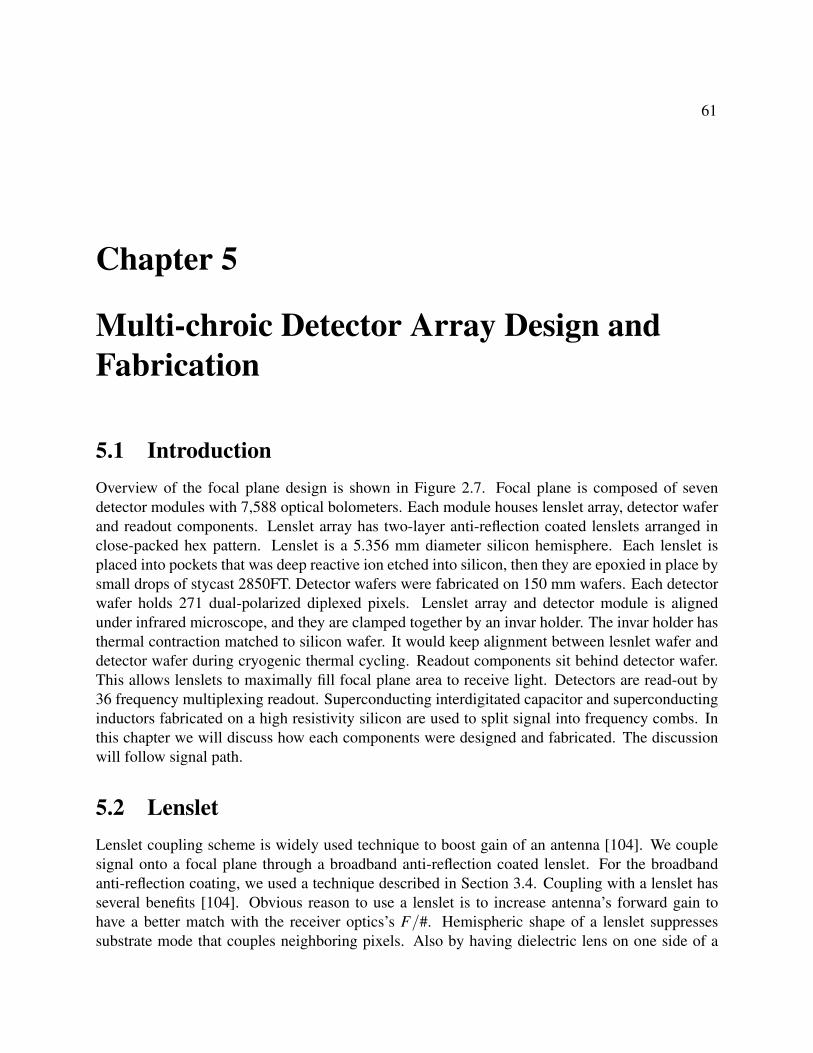
61
Chapter 5
Multi-chroic Detector Array Design andFabrication
5.1 IntroductionOverview of the focal plane design is shown in Figure 2.7. Focal plane is composed of sevendetector modules with 7,588 optical bolometers. Each module houses lenslet array, detector waferand readout components. Lenslet array has two-layer anti-reflection coated lenslets arranged inclose-packed hex pattern. Lenslet is a 5.356 mm diameter silicon hemisphere. Each lenslet isplaced into pockets that was deep reactive ion etched into silicon, then they are epoxied in place bysmall drops of stycast 2850FT. Detector wafers were fabricated on 150 mm wafers. Each detectorwafer holds 271 dual-polarized diplexed pixels. Lenslet array and detector module is alignedunder infrared microscope, and they are clamped together by an invar holder. The invar holder hasthermal contraction matched to silicon wafer. It would keep alignment between lesnlet wafer anddetector wafer during cryogenic thermal cycling. Readout components sit behind detector wafer.This allows lenslets to maximally fill focal plane area to receive light. Detectors are read-out by36 frequency multiplexing readout. Superconducting interdigitated capacitor and superconductinginductors fabricated on a high resistivity silicon are used to split signal into frequency combs. Inthis chapter we will discuss how each components were designed and fabricated. The discussionwill follow signal path.
5.2 LensletLenslet coupling scheme is widely used technique to boost gain of an antenna [104]. We couplesignal onto a focal plane through a broadband anti-reflection coated lenslet. For the broadbandanti-reflection coating, we used a technique described in Section 3.4. Coupling with a lenslet hasseveral benefits [104]. Obvious reason to use a lenslet is to increase antenna’s forward gain tohave a better match with the receiver optics’s F/#. Hemispheric shape of a lenslet suppressessubstrate mode that couples neighboring pixels. Also by having dielectric lens on one side of a
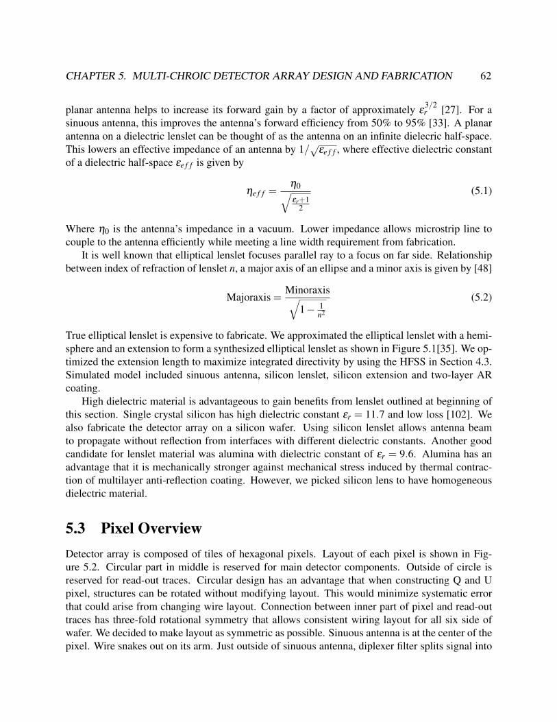
CHAPTER 5. MULTI-CHROIC DETECTOR ARRAY DESIGN AND FABRICATION 62
planar antenna helps to increase its forward gain by a factor of approximately ε3/2r [27]. For a
sinuous antenna, this improves the antenna’s forward efficiency from 50% to 95% [33]. A planarantenna on a dielectric lenslet can be thought of as the antenna on an infinite dielecric half-space.This lowers an effective impedance of an antenna by 1/√εe f f , where effective dielectric constantof a dielectric half-space εe f f is given by
ηe f f =η0√εr+1
2
(5.1)
Where η0 is the antenna’s impedance in a vacuum. Lower impedance allows microstrip line tocouple to the antenna efficiently while meeting a line width requirement from fabrication.
It is well known that elliptical lenslet focuses parallel ray to a focus on far side. Relationshipbetween index of refraction of lenslet n, a major axis of an ellipse and a minor axis is given by [48]
Majoraxis =Minoraxis√
1− 1n2
(5.2)
True elliptical lenslet is expensive to fabricate. We approximated the elliptical lenslet with a hemi-sphere and an extension to form a synthesized elliptical lenslet as shown in Figure 5.1[35]. We op-timized the extension length to maximize integrated directivity by using the HFSS in Section 4.3.Simulated model included sinuous antenna, silicon lenslet, silicon extension and two-layer ARcoating.
High dielectric material is advantageous to gain benefits from lenslet outlined at beginning ofthis section. Single crystal silicon has high dielectric constant εr = 11.7 and low loss [102]. Wealso fabricate the detector array on a silicon wafer. Using silicon lenslet allows antenna beamto propagate without reflection from interfaces with different dielectric constants. Another goodcandidate for lenslet material was alumina with dielectric constant of εr = 9.6. Alumina has anadvantage that it is mechanically stronger against mechanical stress induced by thermal contrac-tion of multilayer anti-reflection coating. However, we picked silicon lens to have homogeneousdielectric material.
5.3 Pixel OverviewDetector array is composed of tiles of hexagonal pixels. Layout of each pixel is shown in Fig-ure 5.2. Circular part in middle is reserved for main detector components. Outside of circle isreserved for read-out traces. Circular design has an advantage that when constructing Q and Upixel, structures can be rotated without modifying layout. This would minimize systematic errorthat could arise from changing wire layout. Connection between inner part of pixel and read-outtraces has three-fold rotational symmetry that allows consistent wiring layout for all six side ofwafer. We decided to make layout as symmetric as possible. Sinuous antenna is at the center of thepixel. Wire snakes out on its arm. Just outside of sinuous antenna, diplexer filter splits signal into
CHAPTER 5. MULTI-CHROIC DETECTOR ARRAY DESIGN AND FABRICATION 63
Figure 5.1: Extension length as a function of dielectric constant of lens [35].
Figure 5.2: CAD of a pixel. Sinuous antenna is at the center of the pixel. Four diplexer filterssurround the sinuous antenna. Four optical bolometers surrounds the filters. Dark bolometers andtest structures surrounds optical bolometers. Twelve pads at the edge of circle connects wiringinside of pixel to on-wafer wiring.

CHAPTER 5. MULTI-CHROIC DETECTOR ARRAY DESIGN AND FABRICATION 64
Figure 5.3: Samples of broadband log-periodic planar antennas. From left: bow-tie antenna, log-spiral antenna, log-periodic antenna and sinuous antenna.
two frequency bands. Two transmission lines cross over before optical power is detected at fouroptical bolometers that surrounds the antenna. Bolometer that is not connected to antenna (darkbolometer) and fabrication test structures surrounds optical bolometers.
5.4 Sinuous Antenna
Sinuous AntennaMultichroic detector design is a extension of successful single frequency design [88, 13]. Mi-crostrip filter defines the final bandwidth of the detector, but the maximum bandwidth of singlefrequency detector was limited by bandwidth of a double slot antenna. O’Brient et al. experi-mented with various kinds of broadband antenna. We found that sinuous antenna met many cri-teria to replace the double slot antenna to increase bandwidth of a pixel. We also changed singlefrequency band-pass filter to multiplexing bandpass filter. We successfully partitioned broadbandsignal into two, three and seven bands [93, 94]. In this thesis various improvements to the designwere made such that detector can be used for the CMB observation. Also this is the first multi-chroic array that was fabricated on 150 mm wafer at Berkeley. Changes were made on fabricationsteps to make successful detector arrays.
Since we fabricate detector using a planar lithography technique, we looked for a broadbandplanar antenna. Some common broadband planar antennas are shown in Figure 5.3. Bow-tieantenna did not have beam shape that met our criteria. Spiral antenna is sensitive to circular po-larization. Log-periodic tooth antenna had high cross-pol and high polarization wobble amplitude.Sinuous antenna stood out as a broadband antenna with many desireble properties. Sinuous an-tenna has sensitivities to two linear polarization, stable input impedance, good beam shape andsmall polarization axis rotation (polarization wobble) amplitude.
Sinuous antenna is a type of broadband log-periodic antenna patented by DuHamel in 1987[32]. Sinuous antenna can be arranged to have N-fold symmetric structure. For linear and circular
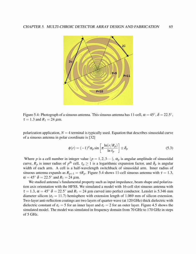
CHAPTER 5. MULTI-CHROIC DETECTOR ARRAY DESIGN AND FABRICATION 65
Figure 5.4: Photograph of a sinuous antenna. This sinuous antenna has 11-cell, α = 45, δ = 22.5,τ = 1.3 and R1 = 24 µm.
polarization application, N = 4 terminal is typically used. Equation that describes sinusoidal curveof a sinuous antenna in polar coordinate is [32]
φ(r) = (−1)pαp sin
[π
ln(r/Rp)
lnτp
]±δp (5.3)
Where p is a cell number in integer value (p = 1,2,3 · · ·), αp is angular amplitude of sinusoidalcurve, Rp is inner radius of pth cell, τp ≥ 1 is a logarithmic expansion factor, and δp is angularwidth of each arm. A cell is a half-wavelength switchback of sinusoidal arm. Inner radius ofsinuous antenna expands as Rp+1 = τRp. Figure 5.4 shows 11-cell sinuous antenna with τ = 1.3,α = 45 δ = 22.5 and R1 = 24 µm.
We studied antenna’s fundamental property such as input impedance, beam shape and polariza-tion axis orientation with the HFSS. We simulated a model with 16-cell slot sinuous antenna withτ = 1.3, α = 45 δ = 22.5 and R1 = 24 µm curved into perfect conductor. Lenslet is 5.346 mmdiameter silicon (εr = 11.7) hemisphere with extension length of 1.069 mm of silicon extension.Two-layer anti-reflection coatings are two layers of quarter-wave (at 120 GHz) thick dielectric withdielectric constant of εr = 5 for an inner layer and εr = 2 for an outer layer. Figure 4.5 shows thesimulated model. The model was simulated in frequency domain from 70 GHz to 170 GHz in stepsof 5 GHz.
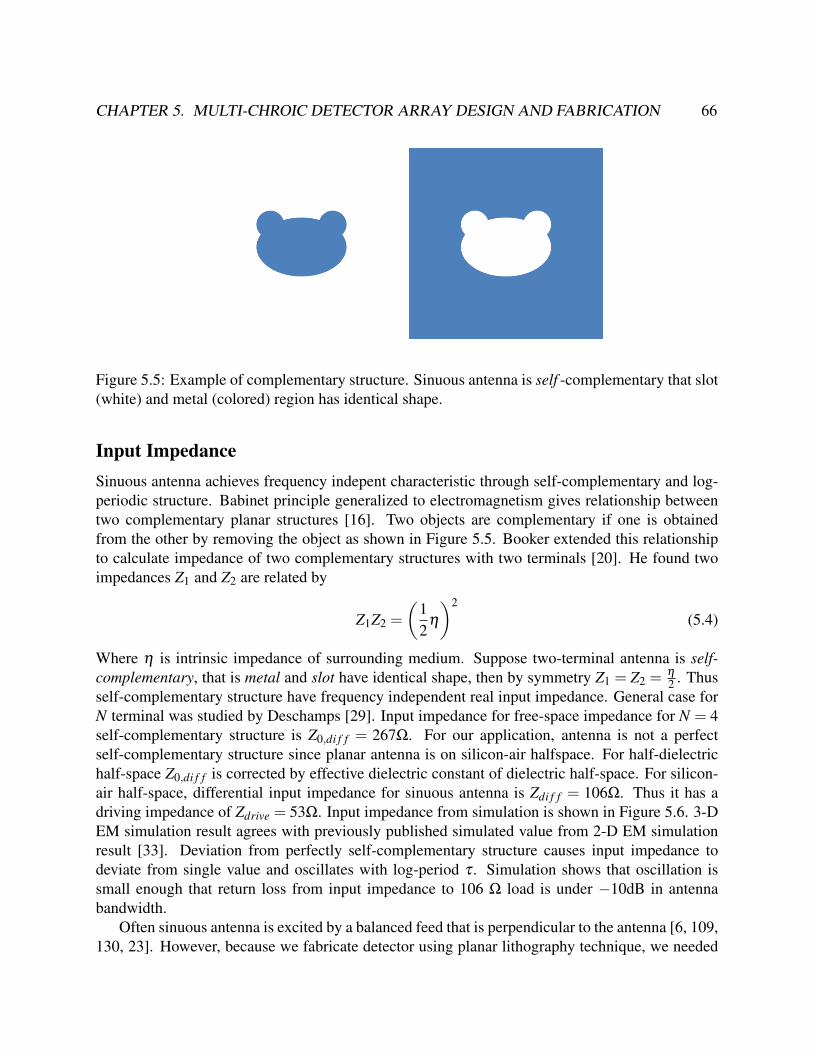
CHAPTER 5. MULTI-CHROIC DETECTOR ARRAY DESIGN AND FABRICATION 66
Figure 5.5: Example of complementary structure. Sinuous antenna is self -complementary that slot(white) and metal (colored) region has identical shape.
Input ImpedanceSinuous antenna achieves frequency indepent characteristic through self-complementary and log-periodic structure. Babinet principle generalized to electromagnetism gives relationship betweentwo complementary planar structures [16]. Two objects are complementary if one is obtainedfrom the other by removing the object as shown in Figure 5.5. Booker extended this relationshipto calculate impedance of two complementary structures with two terminals [20]. He found twoimpedances Z1 and Z2 are related by
Z1Z2 =
(12
η
)2
(5.4)
Where η is intrinsic impedance of surrounding medium. Suppose two-terminal antenna is self-complementary, that is metal and slot have identical shape, then by symmetry Z1 = Z2 =
η
2 . Thusself-complementary structure have frequency independent real input impedance. General case forN terminal was studied by Deschamps [29]. Input impedance for free-space impedance for N = 4self-complementary structure is Z0,di f f = 267Ω. For our application, antenna is not a perfectself-complementary structure since planar antenna is on silicon-air halfspace. For half-dielectrichalf-space Z0,di f f is corrected by effective dielectric constant of dielectric half-space. For silicon-air half-space, differential input impedance for sinuous antenna is Zdi f f = 106Ω. Thus it has adriving impedance of Zdrive = 53Ω. Input impedance from simulation is shown in Figure 5.6. 3-DEM simulation result agrees with previously published simulated value from 2-D EM simulationresult [33]. Deviation from perfectly self-complementary structure causes input impedance todeviate from single value and oscillates with log-period τ . Simulation shows that oscillation issmall enough that return loss from input impedance to 106 Ω load is under −10dB in antennabandwidth.
Often sinuous antenna is excited by a balanced feed that is perpendicular to the antenna [6, 109,130, 23]. However, because we fabricate detector using planar lithography technique, we needed
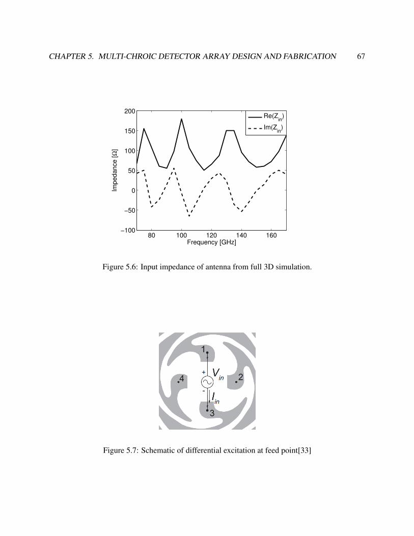
CHAPTER 5. MULTI-CHROIC DETECTOR ARRAY DESIGN AND FABRICATION 67
80 100 120 140 160−100
−50
0
50
100
150
200
Frequency [GHz]
Impedance [
Ω]
Re(Z
in)
Im(Zin
)
Figure 5.6: Input impedance of antenna from full 3D simulation.
Figure 5.7: Schematic of differential excitation at feed point[33]

CHAPTER 5. MULTI-CHROIC DETECTOR ARRAY DESIGN AND FABRICATION 68
0 2 4 6 8 100
10
20
30
40
50
60
70
Strip Width [um]
Impedance [
Ω]
10 20 30 40 50 60 70 800
2
4
6
8
10
Strip Width [um]
Impedance [
Ω]
Figure 5.8: Impedance of niobium microstrip line with 0.5 µm thick silicon oxide (εr = 3.8) asfunctoin of strip width.
a way to feed antenna with planar technology. Since we curve out slots in ground plane, there isa continuous ground plane that extends beyond the antenna. Thus we solved the issue by usingmetallic arms of sinuous antenna as ground planes for microstrip lines. We then covered antennawith a layer of silicon dioxide as insulating layer with a niobium strip on top to form a microstripline as shown in Figure 5.7.
We designed differentially fed microstripline to have matching impedance to antenna’s drivingimpedance (53Ω). We calculated impedance of microstrip line as a function of strip width with su-perconducting niobium ground plane, 0.5 um thick silicon dioxide insulator and superconductingniobium strip. We calculated characteristic impedance of microstripline while taking into pene-tration depth of superconductor into effect following [127, 131]. Characteristic impedance versusstrip line width is plotted in Figure 5.8
Mirostrip line needs to be 1.3 µm wide to couple efficiently to antenna. 1.3 µm structure isdifficult to make during fabrication as lines become thinner than design during plasma etching. Idesigned strip at 2.0 µm, and relied on the thinning effect of the plasma etch with small amountof oxygen gas. We can reliably etch line width to be between 1 µm to 2 µm micron. Reflection issmall for line width between 1 µm and 2 µm as shown in Figure 5.9.
2.0 µm line is still challenging width for the fabrication. Previously fabricated sinuous detec-tors [93] used 0.6 µm thick niobium strip to clear step coverage between top niboium layer and0.5 µm thick silicon oxide layer. Etching 0.6 µm thick metal while maintaining 2.0 µm width wasa challenge. To make fabrication more robust, we created a design that removed all vias betweenstrip layer and ground plane layer. Then we reduced the thickness of niobium strip to 0.3 µm.Lower limit on niobium thickness comes from superconducting transmission line’s wave speed asa function of metal thickness. Phase velocity is a function of penetration depth [79]. Penetrationdepth settles to a constant value for a superconducting metal thicker than 5 times London pene-tration depth. Niobium’s London penetration depth is 39± 5 nm [86]. Thus minimum thickness
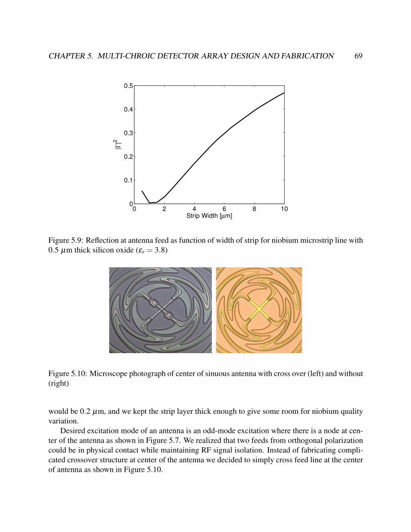
CHAPTER 5. MULTI-CHROIC DETECTOR ARRAY DESIGN AND FABRICATION 69
0 2 4 6 8 100
0.1
0.2
0.3
0.4
0.5
Strip Width [µm]
|Γ|2
Figure 5.9: Reflection at antenna feed as function of width of strip for niobium microstrip line with0.5 µm thick silicon oxide (εr = 3.8)
Figure 5.10: Microscope photograph of center of sinuous antenna with cross over (left) and without(right)
would be 0.2 µm, and we kept the strip layer thick enough to give some room for niobium qualityvariation.
Desired excitation mode of an antenna is an odd-mode excitation where there is a node at cen-ter of the antenna as shown in Figure 5.7. We realized that two feeds from orthogonal polarizationcould be in physical contact while maintaining RF signal isolation. Instead of fabricating compli-cated crossover structure at center of the antenna we decided to simply cross feed line at the centerof antenna as shown in Figure 5.10.
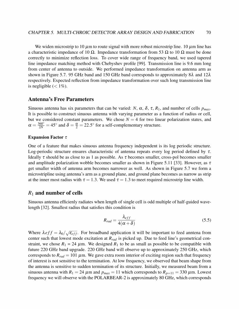
CHAPTER 5. MULTI-CHROIC DETECTOR ARRAY DESIGN AND FABRICATION 70
We widen microstrip to 10 µm to route signal with more robust microstrip line. 10 µm line hasa characteristic impedance of 10 Ω. Impedance transformation from 53 Ω to 10 Ω must be donecorrectly to minimize reflection loss. To cover wide range of frequency band, we used taperedline impedance matching method with Chebyshev profile [99]. Transmission line is 9.6 mm longfrom center of antenna to outside. We performed impedance transformation on antenna arm asshown in Figure 5.7. 95 GHz band and 150 GHz band corresponds to approximately 8λ and 12λ
respectively. Expected reflection from impedance transformation over such long transmission lineis negligible (< 1%).
Antenna’s Free ParametersSinuous antenna has six parameters that can be varied: N, α , δ , τ , R1, and number of cells pmax.It is possible to construct sinuous antenna with varying parameter as a function of radius or cell,but we considered constant parameters. We chose N = 4 for two linear polarization states, andα = 360
2N = 45 and δ = α
2 = 22.5 for a self-complementary structure.
Expansion Factor τ
One of a feature that makes sinuous antenna frequency independent is its log periodic structure.Log-periodic structure ensures characteristic of antenna repeats every log period defined by τ .Ideally τ should be as close to as 1 as possible. As τ becomes smaller, cross-pol becomes smallerand amplitude polarization wobble becomes smaller as shown in Figure 5.11 [33]. However, as τ
get smaller width of antenna arm becomes narrower as well. As shown in Figure 5.7 we form amicrostripline using antenna’s arm as a ground plane, and ground plane becomes as narrow as stripat the inner most radius with τ = 1.3. We used τ = 1.3 to meet required microstrip line width.
R1 and number of cellsSinuous antenna efficienly radiates when length of single cell is odd multiple of half-guided wave-length [32]. Smallest radius that satisfies this condition is
Rrad =λe f f
4(α +δ )(5.5)
Where λe f f = λ0/√
εe f f . For broadband application it will be important to feed anntena fromcenter such that lowest mode excitation at Rrad is picked up. Due to feed line’s geometrical con-straint, we chose R1 = 24 µm. We designed R1 to be as small as possible to be compatible withfuture 220 GHz band upgrade. 220 GHz band will observe up to approximately 250 GHz, whichcorresponds to Rrad = 101 µm. We gave extra room interior of exciting region such that frequencyof interest is not sensitive to the termination. At low frequency, we observed that beam shape fromthe antenna is sensitive to sudden termination of its structure. Initially, we measured beam from asinuous antenna with R1 = 24 µm and pmax = 11 which corresponds to Rp=11 = 330 µm. Lowestfrequency we will observe with the POLARBEAR-2 is approximately 80 GHz, which corresponds
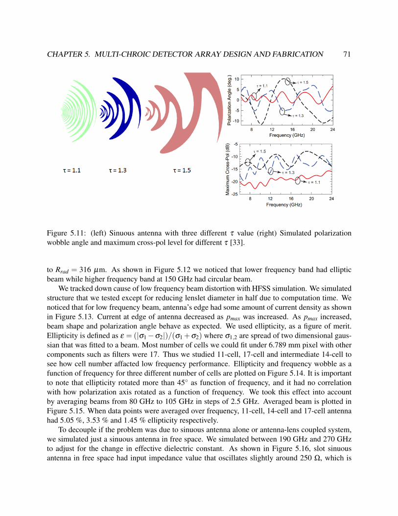
CHAPTER 5. MULTI-CHROIC DETECTOR ARRAY DESIGN AND FABRICATION 71
Figure 5.11: (left) Sinuous antenna with three different τ value (right) Simulated polarizationwobble angle and maximum cross-pol level for different τ [33].
to Rrad = 316 µm. As shown in Figure 5.12 we noticed that lower frequency band had ellipticbeam while higher frequency band at 150 GHz had circular beam.
We tracked down cause of low frequency beam distortion with HFSS simulation. We simulatedstructure that we tested except for reducing lenslet diameter in half due to computation time. Wenoticed that for low frequency beam, antenna’s edge had some amount of current density as shownin Figure 5.13. Current at edge of antenna decreased as pmax was increased. As pmax increased,beam shape and polarization angle behave as expected. We used ellipticity, as a figure of merit.Ellipticity is defined as ε = (|σ1−σ2|)/(σ1 +σ2) where σ1,2 are spread of two dimensional gaus-sian that was fitted to a beam. Most number of cells we could fit under 6.789 mm pixel with othercomponents such as filters were 17. Thus we studied 11-cell, 17-cell and intermediate 14-cell tosee how cell number affacted low frequency performance. Ellipticity and frequency wobble as afunction of frequency for three different number of cells are plotted on Figure 5.14. It is importantto note that ellipticity rotated more than 45 as function of frequency, and it had no correlationwith how polarization axis rotated as a function of frequency. We took this effect into accountby averaging beams from 80 GHz to 105 GHz in steps of 2.5 GHz. Averaged beam is plotted inFigure 5.15. When data points were averaged over frequency, 11-cell, 14-cell and 17-cell antennahad 5.05 %, 3.53 % and 1.45 % ellipticity respectively.
To decouple if the problem was due to sinuous antenna alone or antenna-lens coupled system,we simulated just a sinuous antenna in free space. We simulated between 190 GHz and 270 GHzto adjust for the change in effective dielectric constant. As shown in Figure 5.16, slot sinuousantenna in free space had input impedance value that oscillates slightly around 250 Ω, which is
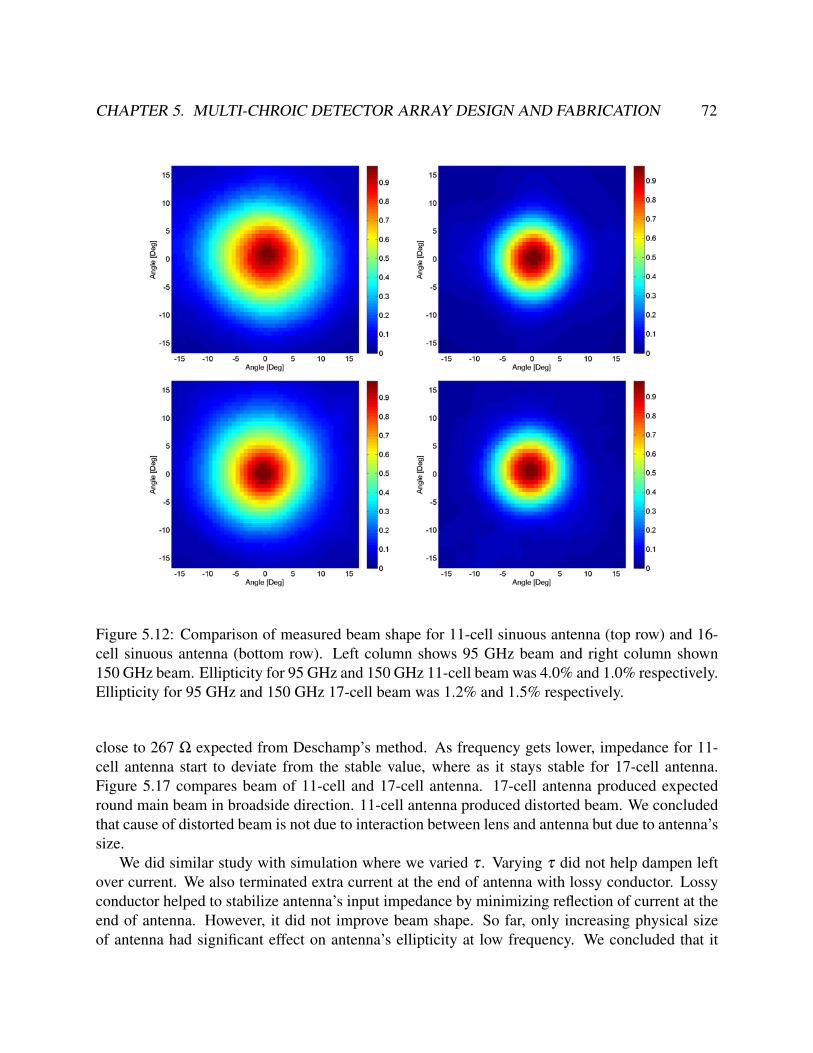
CHAPTER 5. MULTI-CHROIC DETECTOR ARRAY DESIGN AND FABRICATION 72
Figure 5.12: Comparison of measured beam shape for 11-cell sinuous antenna (top row) and 16-cell sinuous antenna (bottom row). Left column shows 95 GHz beam and right column shown150 GHz beam. Ellipticity for 95 GHz and 150 GHz 11-cell beam was 4.0% and 1.0% respectively.Ellipticity for 95 GHz and 150 GHz 17-cell beam was 1.2% and 1.5% respectively.
close to 267 Ω expected from Deschamp’s method. As frequency gets lower, impedance for 11-cell antenna start to deviate from the stable value, where as it stays stable for 17-cell antenna.Figure 5.17 compares beam of 11-cell and 17-cell antenna. 17-cell antenna produced expectedround main beam in broadside direction. 11-cell antenna produced distorted beam. We concludedthat cause of distorted beam is not due to interaction between lens and antenna but due to antenna’ssize.
We did similar study with simulation where we varied τ . Varying τ did not help dampen leftover current. We also terminated extra current at the end of antenna with lossy conductor. Lossyconductor helped to stabilize antenna’s input impedance by minimizing reflection of current at theend of antenna. However, it did not improve beam shape. So far, only increasing physical sizeof antenna had significant effect on antenna’s ellipticity at low frequency. We concluded that it
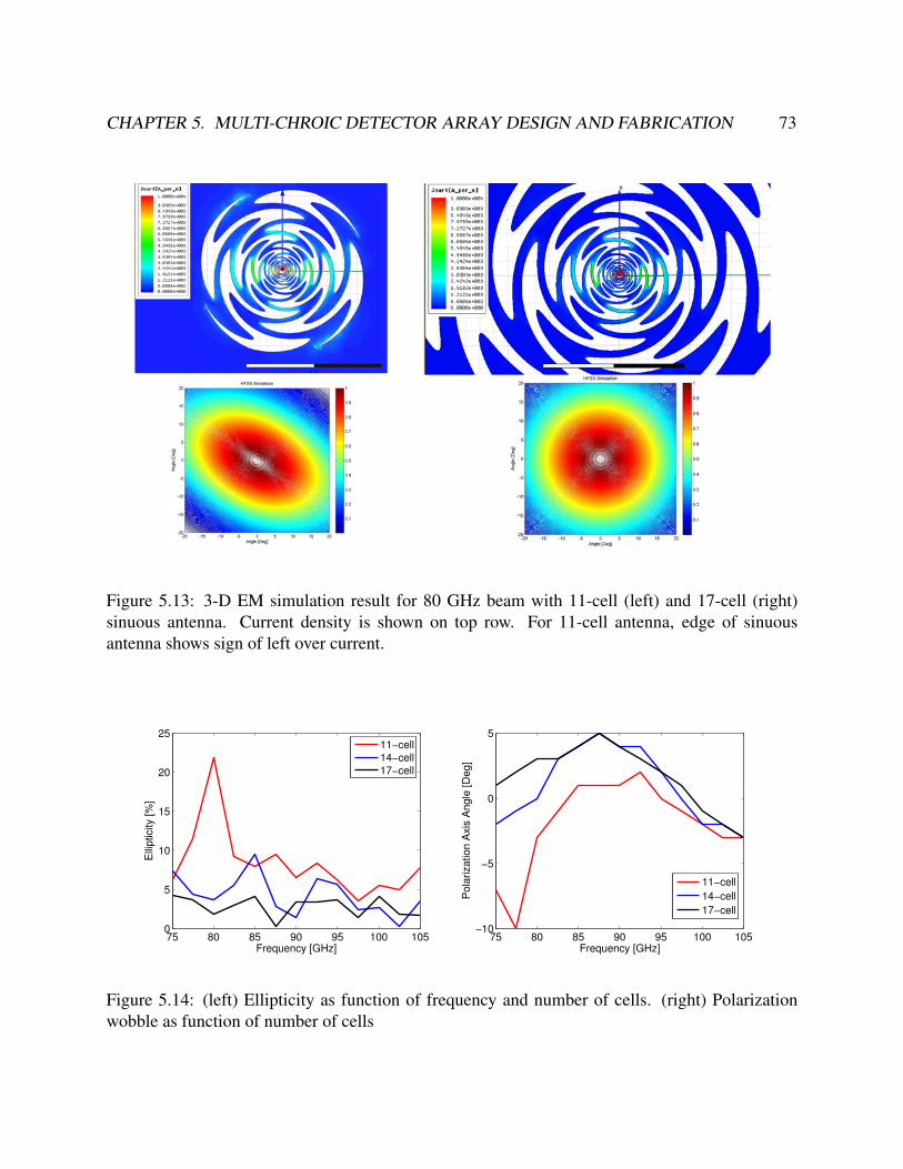
CHAPTER 5. MULTI-CHROIC DETECTOR ARRAY DESIGN AND FABRICATION 73
Figure 5.13: 3-D EM simulation result for 80 GHz beam with 11-cell (left) and 17-cell (right)sinuous antenna. Current density is shown on top row. For 11-cell antenna, edge of sinuousantenna shows sign of left over current.
75 80 85 90 95 100 1050
5
10
15
20
25
Frequency [GHz]
Elli
pticity [%
]
11−cell
14−cell
17−cell
75 80 85 90 95 100 105−10
−5
0
5
Frequency [GHz]
Pola
rization A
xis
Angle
[D
eg]
11−cell
14−cell
17−cell
Figure 5.14: (left) Ellipticity as function of frequency and number of cells. (right) Polarizationwobble as function of number of cells

CHAPTER 5. MULTI-CHROIC DETECTOR ARRAY DESIGN AND FABRICATION 74
Figure 5.15: Band-averaged beam from 75 GHz to 105 GHz. From left, 11-cell, 14-cell and 17-cellsinuous antenna’s beam is shown. Beam had 5.05%, 3.53% and 1.45% ellipticity respectively.
190 200 210 220 230 240 250 260 270−100
0
100
200
300
400
Frequency [GHz]
Impedance [
Ω]
17−Cell Re(Z
in)
17−Cell Im(Zin
)
11−Cell Re(Zin
)
11−Cell Im(Zin
)
Figure 5.16: Input impedance of sinuous antenna in vacuum as function of frequency. 11-Cellantenna’s impedance start to deviate from expected 267 Ω of self-complementary antenna at lowfrequency.
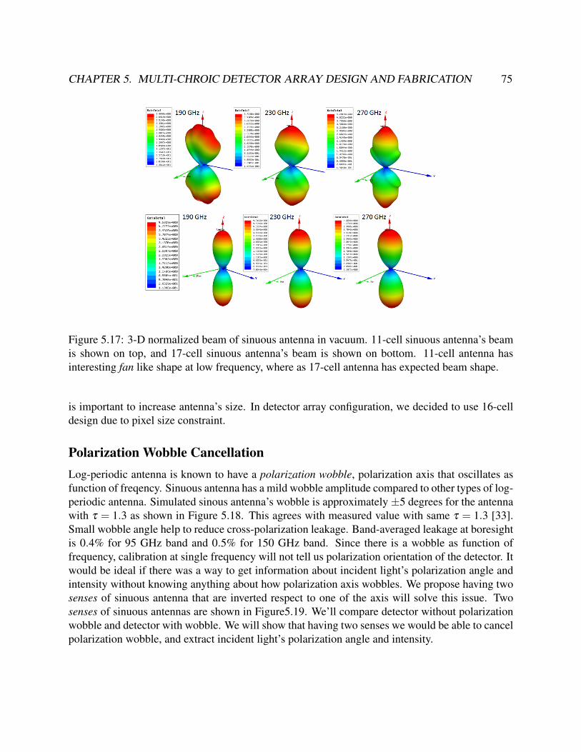
CHAPTER 5. MULTI-CHROIC DETECTOR ARRAY DESIGN AND FABRICATION 75
Figure 5.17: 3-D normalized beam of sinuous antenna in vacuum. 11-cell sinuous antenna’s beamis shown on top, and 17-cell sinuous antenna’s beam is shown on bottom. 11-cell antenna hasinteresting fan like shape at low frequency, where as 17-cell antenna has expected beam shape.
is important to increase antenna’s size. In detector array configuration, we decided to use 16-celldesign due to pixel size constraint.
Polarization Wobble CancellationLog-periodic antenna is known to have a polarization wobble, polarization axis that oscillates asfunction of freqency. Sinuous antenna has a mild wobble amplitude compared to other types of log-periodic antenna. Simulated sinous antenna’s wobble is approximately ±5 degrees for the antennawith τ = 1.3 as shown in Figure 5.18. This agrees with measured value with same τ = 1.3 [33].Small wobble angle help to reduce cross-polarization leakage. Band-averaged leakage at boresightis 0.4% for 95 GHz band and 0.5% for 150 GHz band. Since there is a wobble as function offrequency, calibration at single frequency will not tell us polarization orientation of the detector. Itwould be ideal if there was a way to get information about incident light’s polarization angle andintensity without knowing anything about how polarization axis wobbles. We propose having twosenses of sinuous antenna that are inverted respect to one of the axis will solve this issue. Twosenses of sinuous antennas are shown in Figure5.19. We’ll compare detector without polarizationwobble and detector with wobble. We will show that having two senses we would be able to cancelpolarization wobble, and extract incident light’s polarization angle and intensity.

CHAPTER 5. MULTI-CHROIC DETECTOR ARRAY DESIGN AND FABRICATION 76
80 100 120 140 160−6
−4
−2
0
2
4
6
Frequency [GHz]
Wo
bb
le A
ng
le [
De
g]
Figure 5.18: (left) Comparison of simulated wobble angle and measurement of the sinuous antennaat 8 GHz to 25 GHz. Discrepancy between simulation and measurement comes from exlusion of10 mil subtrate layer (εr = 10.2) in simulation [33]. (right) 3-D EM simulation result between70 GHz to 170 GHz.
Figure 5.19: Two different sense of the sinuous antenna
Review of Detector without Wobble
We picked double slot dipole antenna as an example of detector without wobble. The antenna’spolarization angle is well defined by its gemetry. Two types of pixels are required to obtain twostokes parameter (Q and U) without polarization modulation device such as half-wave plate. Asshon in Figure 5.20, Q pixel is defined as a pixel with polarization axes aligned to 0 degree and90 degree, and U pixel is defined as a pixel with polarization axes aligned to 45 degree and -45degree. In following discussion, we focused just on polarized portion of the light. Light can havenon-polarized component but it would not affect the result so we omitted it in our discussion.Suppose incident light has polarization angle θ(ν) respect to the detector with polarized E-field
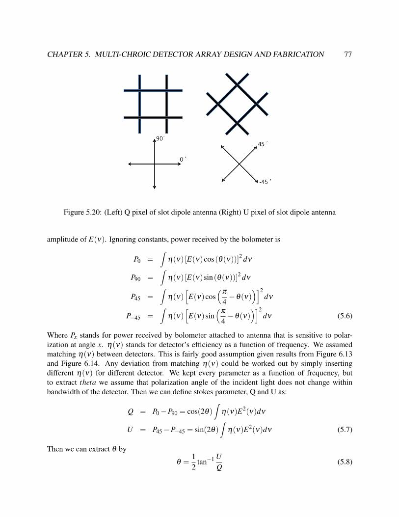
CHAPTER 5. MULTI-CHROIC DETECTOR ARRAY DESIGN AND FABRICATION 77
Figure 5.20: (Left) Q pixel of slot dipole antenna (Right) U pixel of slot dipole antenna
amplitude of E(ν). Ignoring constants, power received by the bolometer is
P0 =∫
η(ν) [E(ν)cos(θ(ν))]2 dν
P90 =∫
η(ν) [E(ν)sin(θ(ν))]2 dν
P45 =∫
η(ν)[E(ν)cos
(π
4−θ(ν)
)]2dν
P−45 =∫
η(ν)[E(ν)sin
(π
4−θ(ν)
)]2dν (5.6)
Where Px stands for power received by bolometer attached to antenna that is sensitive to polar-ization at angle x. η(ν) stands for detector’s efficiency as a function of frequency. We assumedmatching η(ν) between detectors. This is fairly good assumption given results from Figure 6.13and Figure 6.14. Any deviation from matching η(ν) could be worked out by simply insertingdifferent η(ν) for different detector. We kept every parameter as a function of frequency, butto extract theta we assume that polarization angle of the incident light does not change withinbandwidth of the detector. Then we can define stokes parameter, Q and U as:
Q = P0−P90 = cos(2θ)∫
η(ν)E2(ν)dν
U = P45−P−45 = sin(2θ)∫
η(ν)E2(ν)dν (5.7)
Then we can extract θ by
θ =12
tan−1 UQ
(5.8)
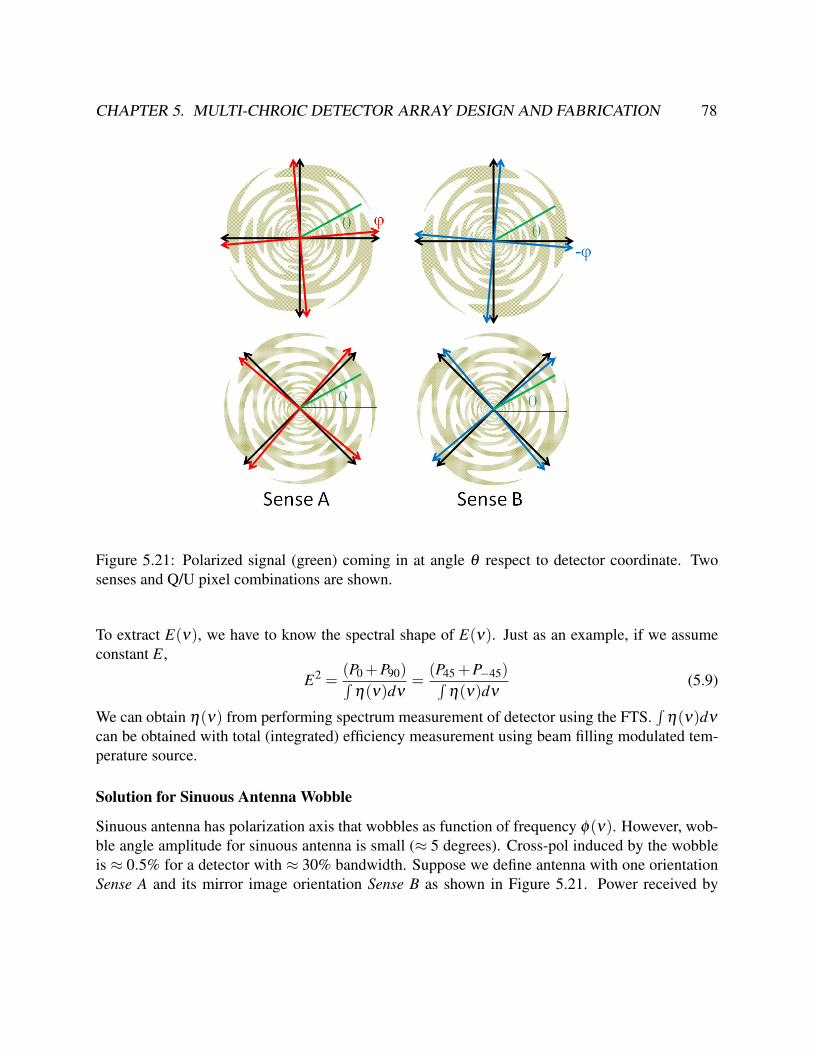
CHAPTER 5. MULTI-CHROIC DETECTOR ARRAY DESIGN AND FABRICATION 78
Figure 5.21: Polarized signal (green) coming in at angle θ respect to detector coordinate. Twosenses and Q/U pixel combinations are shown.
To extract E(ν), we have to know the spectral shape of E(ν). Just as an example, if we assumeconstant E,
E2 =(P0 +P90)∫
η(ν)dν=
(P45 +P−45)∫η(ν)dν
(5.9)
We can obtain η(ν) from performing spectrum measurement of detector using the FTS.∫
η(ν)dν
can be obtained with total (integrated) efficiency measurement using beam filling modulated tem-perature source.
Solution for Sinuous Antenna Wobble
Sinuous antenna has polarization axis that wobbles as function of frequency φ(ν). However, wob-ble angle amplitude for sinuous antenna is small (≈ 5 degrees). Cross-pol induced by the wobbleis ≈ 0.5% for a detector with ≈ 30% bandwidth. Suppose we define antenna with one orientationSense A and its mirror image orientation Sense B as shown in Figure 5.21. Power received by
CHAPTER 5. MULTI-CHROIC DETECTOR ARRAY DESIGN AND FABRICATION 79
bolometers for polarized light with polarization angle of θ be:
PA0 =∫
η(ν) [E(ν)cos(θ(ν)−φ(ν))]2 dν
PA90 =∫
η(ν) [E(ν)sin(θ(ν)−φ(ν))]2 dν
PA45 =∫
η(ν)[E(ν)cos
(π
4−θ(ν)+φ(ν)
)]2dν
PA−45 =∫
η(ν)[E(ν)sin
(π
4−θ(ν)+φ(ν)
)]2dν
PB0 =∫
η(ν) [E(ν)cos(θ(ν)+φ(ν))]2 dν
PB90 =∫
η(ν) [E(ν)sin(θ(ν)+φ(ν))]2 dν
PB45 =∫
η(ν)[E(ν)cos
(π
4−θ(ν)−φ(ν)
)]2dν
PB−45 =∫
η(ν)[E(ν)sin
(π
4−θ(ν)−φ(ν)
)]2dν (5.10)
We do same operation as we did with double slot dipole antenna to get Q and U parameter withwobble. We first subtract signal from two orthogonal arms of antenna as we did with doubleslot dipole example. It is important that this operation happens first to cancel out common modefluctuation such as change in atmospheric loading. We again assume θ is constant across band,
QA = PA0−PA90 =∫
η(ν)E2(ν)cos [2(θ −φ(ν))]dν
QB = PB0−PB90 =∫
η(ν)E2(ν)cos [2(θ +φ(ν))]dν
UA = PA45−PA−45 =∫
η(ν)E2(ν)sin [2(θ −φ(ν))]dν
UB = PB45−PB−45 =∫
η(ν)E2(ν)sin [2(θ +φ(ν))]dν (5.11)
We use trigonometry identity to decouple θ and φ
QA =∫
η(ν)E2(ν) [cos(2θ)cos(2φ(ν))+ sin(2θ)sin(2φ(ν))]dν
QB =∫
η(ν)E2(ν) [cos(2θ)cos(2φ(ν))− sin(2θ)sin(2φ(ν))]dν
UA =∫
η(ν)E2(ν) [sin(2θ)cos(2φ(ν))− cos(2θ)sin(2φ(ν))]dν
UB =∫
η(ν)E2(ν) [sin(2θ)cos(φ(ν))+ cos(2θ)sin(2φ(ν))]dν (5.12)
CHAPTER 5. MULTI-CHROIC DETECTOR ARRAY DESIGN AND FABRICATION 80
By subtracting and adding QA and QB (also UA and UB), we get
Q1 =QA +QB
2= cos(2θ)
∫η(ν)E2(ν)cos(2φ(ν))dν
Q2 =UB−UA
2= cos(2θ)
∫η(ν)E2(ν)sin(2φ(ν))dν
U1 =QA−QB
2= sin(2θ)
∫η(ν)E2(ν)sin(2φ(ν))dν
U2 =UB +UA
2= sin(2θ)
∫η(ν)E2(ν)cos(2φ(ν))dν (5.13)
Then we can get θ by dividing taking ratio of U1,2 and Q2,1.
θ =12
tan−1 U1,2
Q2,1(5.14)
We can get to E(ν) in same way we obtained E(ν) for double slot dipole,∫η(ν)E2(ν)dν = PA0 +PA90 = PA45 +PA−45 = PB0 +PB90 = PB45 +PB−45 (5.15)
Just like the case of detector without wobble, we have to know the spectrum shape of E(ν). Justas an example if we assume constant E(ν) within band, E is
E2 =PA0 +PA90∫
η(ν)dν=
PA45 +PA−45∫η(ν)dν
=PB0 +PB90∫
η(ν)dν=
PB45 +PB−45∫η(ν)dν
(5.16)
We can obtain η(ν) from performing spectrum measurement of detector using the FTS.∫
η(ν)dν
can be obtained with total (integrated) efficiency measurement using beam filling modulated tem-perature source.
How to Calibrate Polarization Angle
Calibration of polarization axis orientation is important for the CMB polarimetry experiment. De-tector with a polarization wobble present a challenge as polarization angle changes as a functionof frequency. As shown in Figure 5.18, polarization angle is sensitive to accurate knowledge ofdielectric constant and extension length. We cannot simply rely on simulation to extrapolate polar-ization axis from one frequency. Thus we need more rubust way of measuring this. By using themirror imaged pair we can calibrate 0 angle accurately.
Suppose we have calibration source with good polarization property and narrow frequencyband such as gunn diode with rectangular horn. As we rotate the calibration source, one pixel willhave peak intensity at polarization angle of φ(ν) and its pair will have peak intensity of −φ(ν)where ν is the frequency of gunn diode. Then angle that is bisecting between φ and −φ is the 0degree angle of the detector.
CHAPTER 5. MULTI-CHROIC DETECTOR ARRAY DESIGN AND FABRICATION 81
Pixel Placement
When populating detector array, it makes sense to populate Q and U pixels side by side for a detec-tor without wobble. Subtraction of two orthogonal polarization happens within pixel to minimizecommon mode noise contribution, then division between Q and U happens. For detectors withwobble, it still does subtraction of two orthogonal polarization signal within same pixel to againminimize common mode noise. But next step is adding or subtracting QA with QB and UA with UB,we placed pixel in order of QA, QB, UA and UB in scan direction.
5.5 Microstrip FilterThe advantage of coupling photon onto microstrip line is an ability to be able to do signal pro-cessing prior to detection at a bolometer. It is this technology that allowed the development ofthe multichroic detector. We explored two types of filters. Distributed filter is made with resonantstructures of transmission line, and lumped filter is made with short high impedance section of lineas an inductor and parallel plate capacitors formed between a ground plane and strip of microstripline.
For a basic filter design, we designed with 3-pole Chebyshev filter since it is a good designwhen optimizing for sensitivity by balancing at in-band loss and roll-off speed [12]. To calculatecomponent values, we followed the insertion loss method [99]. Then we followed Pozar to trans-form calculated values to distributed stub filters. For lumped filters, we followed O’Brient andKumar when transforming calculated components values to planar designs [93, 66, 67]. After cal-culating geometrical design, we optimized the design with 2.5 dimension EM simulator (Sonnet)to account for parasitics. We simulated effect of superconductor by adding 0.13 pH/ surfaceimpedance [62].
Basic Filter DesignTo calculate components’ value, we used the insertion loss method. First we define power loss ratioPLR = 1/(1−|Γ(ω)|2) that is defined as power available from source divided by power deliveredto load. We then specify functional form of PLR for different type of filters. Chebyshev filter is atype of filter that has a sharper cut off but has ripples in passband. Its PLR is defined as
PLR = 1+ k2T 2N
(ω
ωc
)(5.17)
Where T 2N
(ω
ωc
)is a Chebyshev polynomial of order N. N is number of reactive element pair for
a band-pass filter equals the order. Chebyshev filter will have ripples of amplitude (1+ k2). ωc isan angular frequency where PLR = (1+ k2). For a third order, 0.5 dB Chevyshev filter power lossratio is explicitly
PLR = 1+(0.35)2
[4(
ω
ωc
)2
−3(
ω
ωc
)2]2
(5.18)

CHAPTER 5. MULTI-CHROIC DETECTOR ARRAY DESIGN AND FABRICATION 82
We calculate input impedance of Nth order low pass filter with a source impedance of 1 Ω asshown in Figure 5.22. Then we calculate input impedance Zin and reflection coefficient Γ =(Zin− 1)/(Zout + 1). We can then calculate PLR = 1/(1− |Γ(ω)|2) in terms of L,C,R,ω . Fi-nally we equate the PLR to Equation 5.18 to extract each element’s value to achieve desired filterperformance. In theory any filter with desired ripple level can be calculated this way. However, inpractice we use tabulated value for common filter type [38]. Odd order of Chebyshev filter couplesto same source and load impedance. Since we are placing filter between two microstriplines thathas equal impedance, we picked a third order. For a third order Chebyshev polynomial, elementalvalues are
g0 = 1.0000g1 = 1.5963g2 = 1.0967g3 = 1.5963g4 = 1.0000 (5.19)
We then scale these elemental values to input imepdance R0 = 10 Ω, and calculate each element inbandpass filter with
Ln =gnR0
ω0∆(series) =
∆R0
gnω0(shunt)
Cn =∆
gnR0ω0(series) =
gn
∆R0ω0(shunt) (5.20)
Ln and Cn are nth element in bandpass filter. Z0 is source impedance, ω0 =√
ωUBωLB is geometricmean of upper and lower bound of bandpass. ∆ = (ωUB−ωLB)/ω0 is a fractional bandwidth.
Distributed FilterDesign steps for distributed filter were shown in Figure 5.22. Loss less shorted quarter wave stubhas an equivalent input impedance as parallel LC circuit. For a parallel LC circuit, input impedanceis
Zin =
(1
jωL+ jωC
)−1
(5.21)
Resonance frequency is ω0 = 1/√
LC. Near resonance, input impedance can be taylor expandedaround ω0. If we let ω = ω0 +δω , with small δω
Zin =
(1−δω/ω0
jω0L+ j(ω0 +δω)C
)−1
=1
j2Cδω(5.22)
Shorted stub with characteristic impedance of Z0 has the input impedance of
Zin = jZ0 tan(β l) (5.23)

CHAPTER 5. MULTI-CHROIC DETECTOR ARRAY DESIGN AND FABRICATION 83
Figure 5.22: Circuit diagram for filter design. a. Low-pass prototype design. b. Band-pass design.c. Circuit diagram for a stub. d. Band-pass design with impedance inverter. e. Lumped filterdesign with T-capacitor network. f. Lumped filter design with π-capacitor network
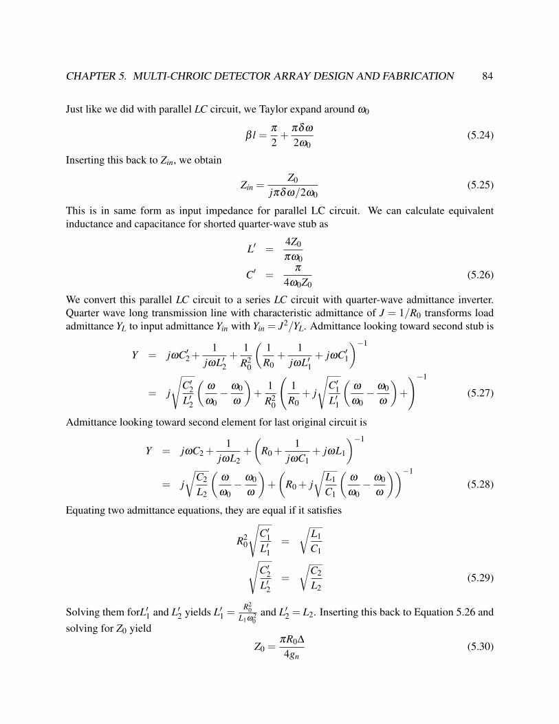
CHAPTER 5. MULTI-CHROIC DETECTOR ARRAY DESIGN AND FABRICATION 84
Just like we did with parallel LC circuit, we Taylor expand around ω0
β l =π
2+
πδω
2ω0(5.24)
Inserting this back to Zin, we obtain
Zin =Z0
jπδω/2ω0(5.25)
This is in same form as input impedance for parallel LC circuit. We can calculate equivalentinductance and capacitance for shorted quarter-wave stub as
L′ =4Z0
πω0
C′ =π
4ω0Z0(5.26)
We convert this parallel LC circuit to a series LC circuit with quarter-wave admittance inverter.Quarter wave long transmission line with characteristic admittance of J = 1/R0 transforms loadadmittance YL to input admittance Yin with Yin = J2/YL. Admittance looking toward second stub is
Y = jωC′2 +1
jωL′2+
1R2
0
(1
R0+
1jωL′1
+ jωC′1
)−1
= j
√C′2L′2
(ω
ω0− ω0
ω
)+
1R2
0
(1
R0+ j
√C′1L′1
(ω
ω0− ω0
ω
)+
)−1
(5.27)
Admittance looking toward second element for last original circuit is
Y = jωC2 +1
jωL2+
(R0 +
1jωC1
+ jωL1
)−1
= j
√C2
L2
(ω
ω0− ω0
ω
)+
(R0 + j
√L1
C1
(ω
ω0− ω0
ω
))−1
(5.28)
Equating two admittance equations, they are equal if it satisfies
R20
√C′1L′1
=
√L1
C1√C′2L′2
=
√C2
L2(5.29)
Solving them forL′1 and L′2 yields L′1 =R2
0L1ω2
0and L′2 = L2. Inserting this back to Equation 5.26 and
solving for Z0 yield
Z0 =πR0∆
4gn(5.30)
CHAPTER 5. MULTI-CHROIC DETECTOR ARRAY DESIGN AND FABRICATION 85
We can then translate to physical dimension by using stub width to impedance ratio from Fig-ure 5.8. For input impedance and fractional bandwidth we are interested in, stub’s impedance canbe as low as few Ω. Such stub is so wide that it could carry higher order mode. To suppress suchmode, we tapered part of stub that connects stub to a transmission line.
In theory we could considered surface inductance effect of superconductor to adjust stub lengthto be quarter wavelength at center frequency. But we noticed that measured band had shift of 10 %with time constant of about few month. We believe that material property on the detector, such askinetic inductance in niobium, is changing as machine condition changes. Thus we adjusted stub’slength using most recent measurement.
For a demonstration of filter design, suppose we are desining three-pole Chebyshev band-passfilter for center frequency of f0 = 147.8 GHz and bandwidth of 26.0%. Using Equation 5.30,impedance of each stubs should be
Z1 = 1.2792Ω
Z2 = 1.8620Ω
Z3 = 1.2792Ω (5.31)
Stub that has this impedance corresponds to
W1 = 86µmW2 = 58µmW3 = 86µm (5.32)
From recent band measurements with the FTS, we know 200 µm corresponds to 150 GHz. Sup-pose that’s close enough for initial design, final design is drawn on Figure 5.23. For diplexerand triplexer design, we first tuned each filter individually. Then they were combined to a singlejunction with some length of microstripline. Length of microstrip line was adjusted in simulatoruntil isolation of approximately -20 dB was achieved. For the diplexer, optimization was fairlyeasy, however, for triplexer this turned out to be very difficult to achieve. Compromise was madebetween bandwidth of each band and inband transmission performance.
Lumped FilterAnother approach to make a filter is to create lumped capacitor and inductor. If we can makearbitual value and type of inductors and capacitors, we will simply make a filter designed in basicfilter design sub-section. However, shunt inductor is difficult to fabricate and some capacitor valueswere too large to fabricate. Thus we went through series of identities to convert shunt LC pair toseries LC pair with impedance transformers. Then we converted T -network to π-network to reducerequired capacitance. Previous realization of such filter had vias from strip layer to ground planelayer [93, 67]. To achieve thinner strip layer for more reliable fine line realization during etching,vias were removed in the final design. Uniformity tolerance, surface inductance tolerance andadjustability study were also taken into account for the final design.
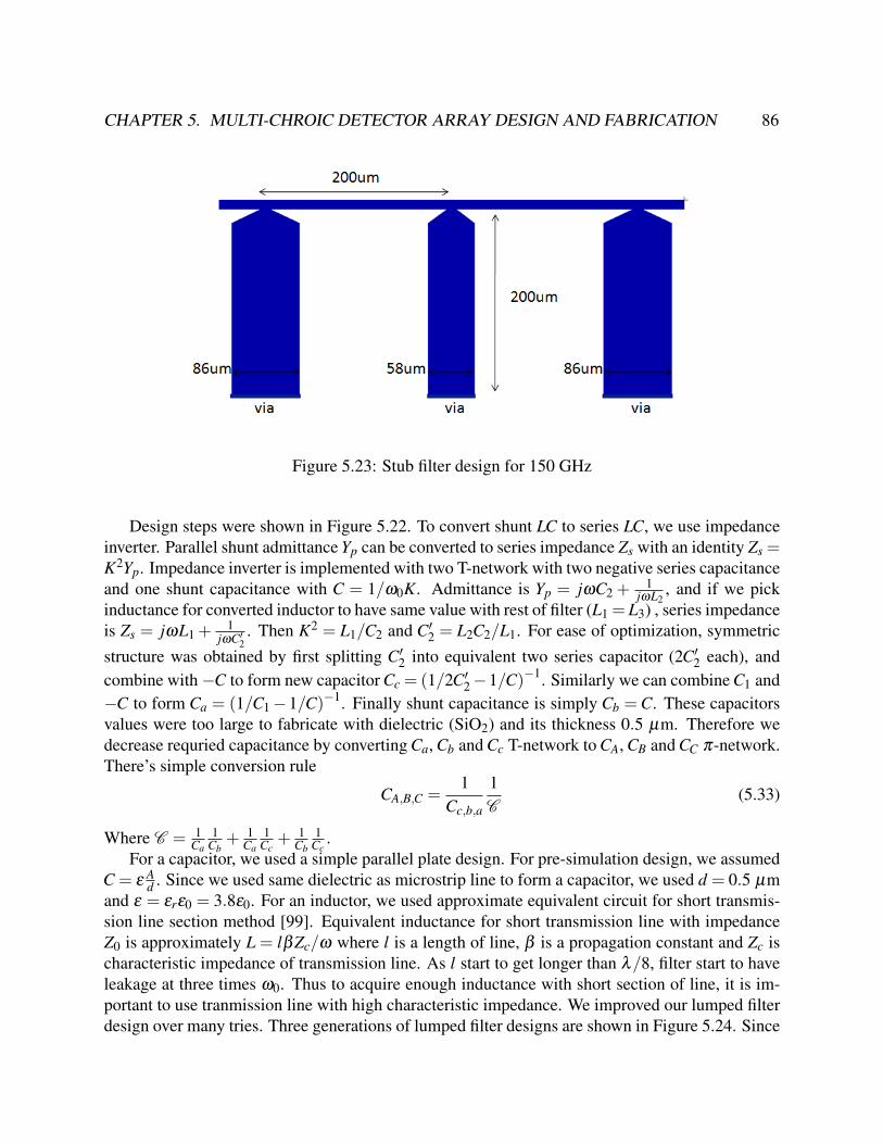
CHAPTER 5. MULTI-CHROIC DETECTOR ARRAY DESIGN AND FABRICATION 86
Figure 5.23: Stub filter design for 150 GHz
Design steps were shown in Figure 5.22. To convert shunt LC to series LC, we use impedanceinverter. Parallel shunt admittance Yp can be converted to series impedance Zs with an identity Zs =K2Yp. Impedance inverter is implemented with two T-network with two negative series capacitanceand one shunt capacitance with C = 1/ω0K. Admittance is Yp = jωC2 +
1jωL2
, and if we pickinductance for converted inductor to have same value with rest of filter (L1 = L3) , series impedanceis Zs = jωL1 +
1jωC′2
. Then K2 = L1/C2 and C′2 = L2C2/L1. For ease of optimization, symmetricstructure was obtained by first splitting C′2 into equivalent two series capacitor (2C′2 each), andcombine with−C to form new capacitor Cc = (1/2C′2−1/C)−1. Similarly we can combine C1 and−C to form Ca = (1/C1−1/C)−1. Finally shunt capacitance is simply Cb = C. These capacitorsvalues were too large to fabricate with dielectric (SiO2) and its thickness 0.5 µm. Therefore wedecrease requried capacitance by converting Ca, Cb and Cc T-network to CA, CB and CC π-network.There’s simple conversion rule
CA,B,C =1
Cc,b,a
1C
(5.33)
Where C = 1Ca
1Cb
+ 1Ca
1Cc
+ 1Cb
1Cc
.For a capacitor, we used a simple parallel plate design. For pre-simulation design, we assumed
C = εAd . Since we used same dielectric as microstrip line to form a capacitor, we used d = 0.5 µm
and ε = εrε0 = 3.8ε0. For an inductor, we used approximate equivalent circuit for short transmis-sion line section method [99]. Equivalent inductance for short transmission line with impedanceZ0 is approximately L = lβZc/ω where l is a length of line, β is a propagation constant and Zc ischaracteristic impedance of transmission line. As l start to get longer than λ/8, filter start to haveleakage at three times ω0. Thus to acquire enough inductance with short section of line, it is im-portant to use tranmission line with high characteristic impedance. We improved our lumped filterdesign over many tries. Three generations of lumped filter designs are shown in Figure 5.24. Since

CHAPTER 5. MULTI-CHROIC DETECTOR ARRAY DESIGN AND FABRICATION 87
Figure 5.24: Three lumped filter design in chronogical order. (top) Lumped filter design with co-planar inductor design with via. (middle) Lumped filter design with microstrip inductor designwithout via. (bottom) Lumped filter design with co-planar inductor design without via
Figure 5.25: Lumped filter design for 150 GHz. Zoomed in CAD for capacitor part shows possibleparasitic capacitance
we already form transmission line with microstrip line, it would be simple if we could form highimpedance microstrip line. We designed lumped inductor with short section of microstrip line asshown in Figure 5.24 (center). However, high impedance is hard to achieve with a microstrip line,and longer line that we used caused higher frequency leakage as shown in Figure 6.15. We used1 µm strip for microstrip lines to form inductors. This caused inductance to be highly dependanton over-etching. To achieve high impedance line, we designed inductor with co-planar waveguide(CPW) as shown in Figure 5.25. CPW is easier to achieve higher imepdance since distance from astrip to a ground plane can be made far. To make a conversion from microstrip line to true co-planarwaveguide, vias are necessary. As we discussed in antenna feed section, we would like to avoidhaving via to keep thickness of strip layer down. Thus we formed quasi-CPW by keeping strip onthe upper layer. Thickness of dielectric is much smaller compared to strip to ground plane width,
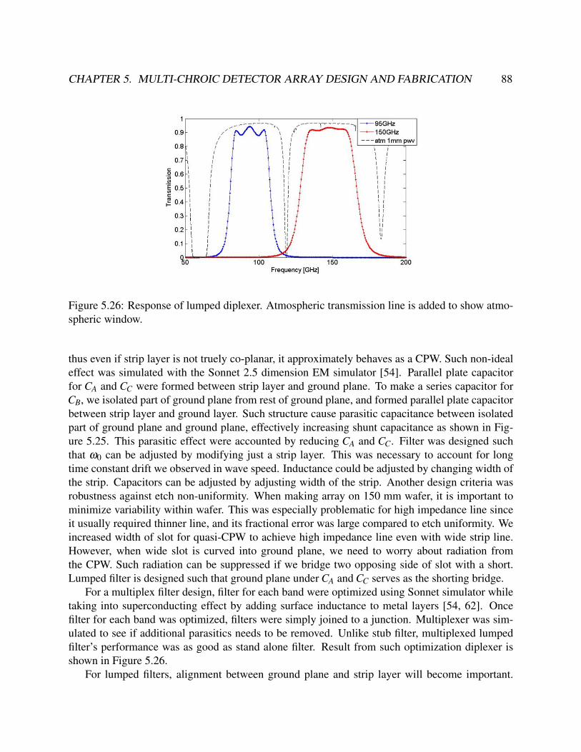
CHAPTER 5. MULTI-CHROIC DETECTOR ARRAY DESIGN AND FABRICATION 88
Figure 5.26: Response of lumped diplexer. Atmospheric transmission line is added to show atmo-spheric window.
thus even if strip layer is not truely co-planar, it approximately behaves as a CPW. Such non-idealeffect was simulated with the Sonnet 2.5 dimension EM simulator [54]. Parallel plate capacitorfor CA and CC were formed between strip layer and ground plane. To make a series capacitor forCB, we isolated part of ground plane from rest of ground plane, and formed parallel plate capacitorbetween strip layer and ground layer. Such structure cause parasitic capacitance between isolatedpart of ground plane and ground plane, effectively increasing shunt capacitance as shown in Fig-ure 5.25. This parasitic effect were accounted by reducing CA and CC. Filter was designed suchthat ω0 can be adjusted by modifying just a strip layer. This was necessary to account for longtime constant drift we observed in wave speed. Inductance could be adjusted by changing width ofthe strip. Capacitors can be adjusted by adjusting width of the strip. Another design criteria wasrobustness against etch non-uniformity. When making array on 150 mm wafer, it is important tominimize variability within wafer. This was especially problematic for high impedance line sinceit usually required thinner line, and its fractional error was large compared to etch uniformity. Weincreased width of slot for quasi-CPW to achieve high impedance line even with wide strip line.However, when wide slot is curved into ground plane, we need to worry about radiation fromthe CPW. Such radiation can be suppressed if we bridge two opposing side of slot with a short.Lumped filter is designed such that ground plane under CA and CC serves as the shorting bridge.
For a multiplex filter design, filter for each band were optimized using Sonnet simulator whiletaking into superconducting effect by adding surface inductance to metal layers [54, 62]. Oncefilter for each band was optimized, filters were simply joined to a junction. Multiplexer was sim-ulated to see if additional parasitics needs to be removed. Unlike stub filter, multiplexed lumpedfilter’s performance was as good as stand alone filter. Result from such optimization diplexer isshown in Figure 5.26.
For lumped filters, alignment between ground plane and strip layer will become important.
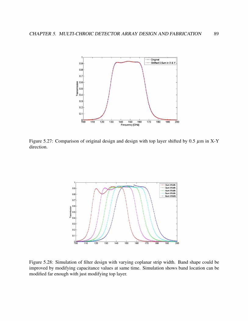
CHAPTER 5. MULTI-CHROIC DETECTOR ARRAY DESIGN AND FABRICATION 89
Figure 5.27: Comparison of original design and design with top layer shifted by 0.5 µm in X-Ydirection.
Figure 5.28: Simulation of filter design with varying coplanar strip width. Band shape could beimproved by modifying capacitance values at same time. Simulation shows band location can bemodified far enough with just modifying top layer.
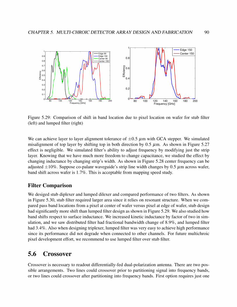
CHAPTER 5. MULTI-CHROIC DETECTOR ARRAY DESIGN AND FABRICATION 90
80 100 120 140 160 180 2000
0.1
0.2
0.3
0.4
0.5
0.6
0.7
0.8
0.9
1
Frequency [GHz]
Effic
iency
Edge 90
Edge 150
Center 90
Center 150
80 100 120 140 160 180 2000
0.2
0.4
0.6
0.8
1
Frequency [GHz]
Effic
iency
Edge 150
Center 150
Figure 5.29: Comparison of shift in band location due to pixel location on wafer for stub filter(left) and lumped filter (right)
We can achieve layer to layer alignment tolerance of ±0.5 µm with GCA stepper. We simulatedmisalignment of top layer by shifting top in both direction by 0.5 µm. As shown in Figure 5.27effect is negligible. We simulated filter’s ability to adjust frequency by modifying just the striplayer. Knowing that we have much more freedom to change capacitance, we studied the effect bychanging inductance by changing strip’s width. As shown in Figure 5.28 center frequency can beadjusted ±10%. Suppose co-palanr waveguide’s strip line width changes by 0.5 µm across wafer,band shift across wafer is 1.7%. This is acceptable from mapping speed study.
Filter ComparisonWe desiged stub diplexer and lumped dilexer and compared performance of two filters. As shownin Figure 5.30, stub filter required larger area since it relies on resonant structure. When we com-pared pass band locations from a pixel at center of wafer versus pixel at edge of wafer, stub designhad significantly more shift than lumped filter design as shown in Figure 5.29. We also studied howband shifts respect to surface inductance. We increased kinetic inductance by factor of two in sim-ulation, and we saw distributed filter had fractional bandwidth change of 8.9%, and lumped filterhad 3.4%. Also when designing triplexer, lumped filter was very easy to achieve high performancesince its performance did not degrade when connected to other channels. For future multichroicpixel development effort, we recommend to use lumped filter over stub filter.
5.6 CrossoverCrossover is necessary to readout differentially-fed dual-polarization antenna. There are two pos-sible arrangements. Two lines could crossover prior to partitioning signal into frequency bands,or two lines could crossover after partitioning into frequency bands. First option requires just one
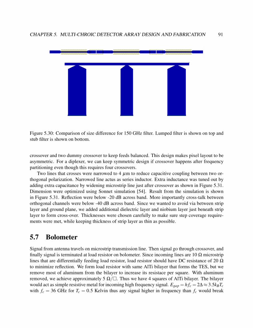
CHAPTER 5. MULTI-CHROIC DETECTOR ARRAY DESIGN AND FABRICATION 91
Figure 5.30: Comparison of size difference for 150 GHz filter. Lumped filter is shown on top andstub filter is shown on bottom.
crossover and two dummy crossover to keep feeds balanced. This design makes pixel layout to beasymmetric. For a diplexer, we can keep symmetric design if crossover happens after frequencypartitioning even though this requires four crossovers.
Two lines that crosses were narrowed to 4 µm to reduce capacitive coupling between two or-thogonal polarization. Narrowed line actus as series inductor. Extra inductance was tuned out byadding extra capacitance by widening microstrip line just after crossover as shown in Figure 5.31.Dimension were optimized using Sonnet simulation [54]. Result from the simulation is shownin Figure 5.31. Reflection were below -20 dB across band. More importantly cross-talk betweenorthogonal channels were below -40 dB across band. Since we wanted to avoid via between striplayer and ground plane, we added additional dielectric layer and niobium layer just beneath striplayer to form cross-over. Thicknesses were chosen carefully to make sure step coverage require-ments were met, while keeping thickness of strip layer as thin as possible.
5.7 BolometerSignal from antenna travels on microstrip transmission line. Then signal go through crossover, andfinally signal is terminated at load resistor on bolometer. Since incoming lines are 10 Ω microstriplines that are differentially feeding load resistor, load resistor should have DC resistance of 20 Ω
to minimize reflection. We form load resistor with same AlTi bilayer that forms the TES, but weremove most of aluminum from the bilayer to increase its resistace per square. With aluminumremoved, we achieve approximately 5 Ω/. Thus we have 4 squares of AlTi bilayer. The bilayerwould act as simple resistive metal for incoming high frequency signal. Egap = h fc = 2∆≈ 3.5kBTcwith fc = 36 GHz for Tc = 0.5 Kelvin thus any signal higher in frequency than fc would break
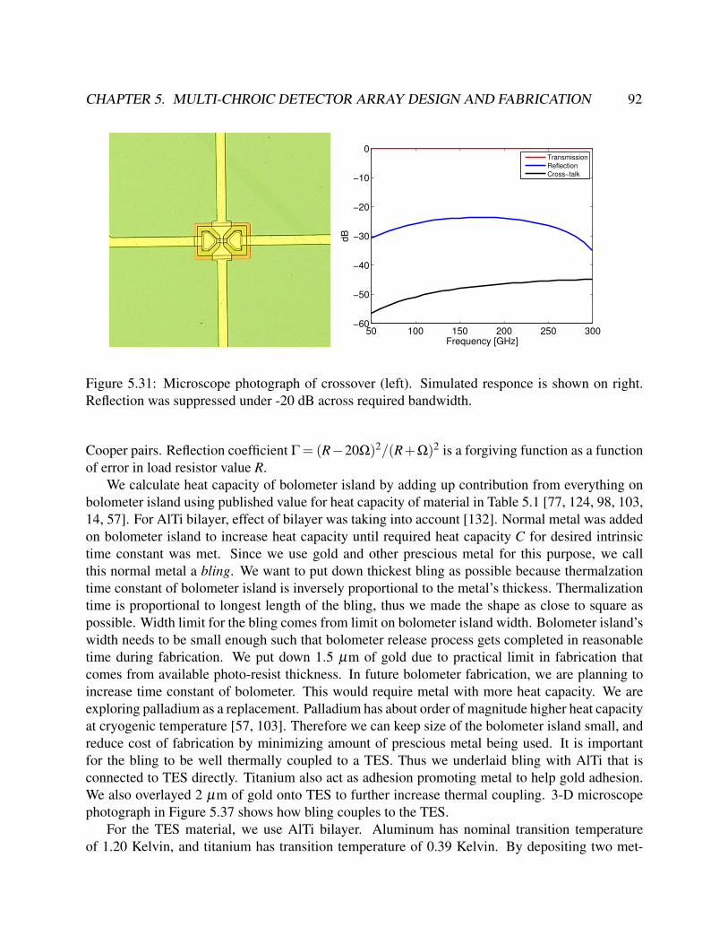
CHAPTER 5. MULTI-CHROIC DETECTOR ARRAY DESIGN AND FABRICATION 92
50 100 150 200 250 300−60
−50
−40
−30
−20
−10
0
Frequency [GHz]d
B
Transmission
Reflection
Cross−talk
Figure 5.31: Microscope photograph of crossover (left). Simulated responce is shown on right.Reflection was suppressed under -20 dB across required bandwidth.
Cooper pairs. Reflection coefficient Γ = (R−20Ω)2/(R+Ω)2 is a forgiving function as a functionof error in load resistor value R.
We calculate heat capacity of bolometer island by adding up contribution from everything onbolometer island using published value for heat capacity of material in Table 5.1 [77, 124, 98, 103,14, 57]. For AlTi bilayer, effect of bilayer was taking into account [132]. Normal metal was addedon bolometer island to increase heat capacity until required heat capacity C for desired intrinsictime constant was met. Since we use gold and other prescious metal for this purpose, we callthis normal metal a bling. We want to put down thickest bling as possible because thermalzationtime constant of bolometer island is inversely proportional to the metal’s thickess. Thermalizationtime is proportional to longest length of the bling, thus we made the shape as close to square aspossible. Width limit for the bling comes from limit on bolometer island width. Bolometer island’swidth needs to be small enough such that bolometer release process gets completed in reasonabletime during fabrication. We put down 1.5 µm of gold due to practical limit in fabrication thatcomes from available photo-resist thickness. In future bolometer fabrication, we are planning toincrease time constant of bolometer. This would require metal with more heat capacity. We areexploring palladium as a replacement. Palladium has about order of magnitude higher heat capacityat cryogenic temperature [57, 103]. Therefore we can keep size of the bolometer island small, andreduce cost of fabrication by minimizing amount of prescious metal being used. It is importantfor the bling to be well thermally coupled to a TES. Thus we underlaid bling with AlTi that isconnected to TES directly. Titanium also act as adhesion promoting metal to help gold adhesion.We also overlayed 2 µm of gold onto TES to further increase thermal coupling. 3-D microscopephotograph in Figure 5.37 shows how bling couples to the TES.
For the TES material, we use AlTi bilayer. Aluminum has nominal transition temperatureof 1.20 Kelvin, and titanium has transition temperature of 0.39 Kelvin. By depositing two met-
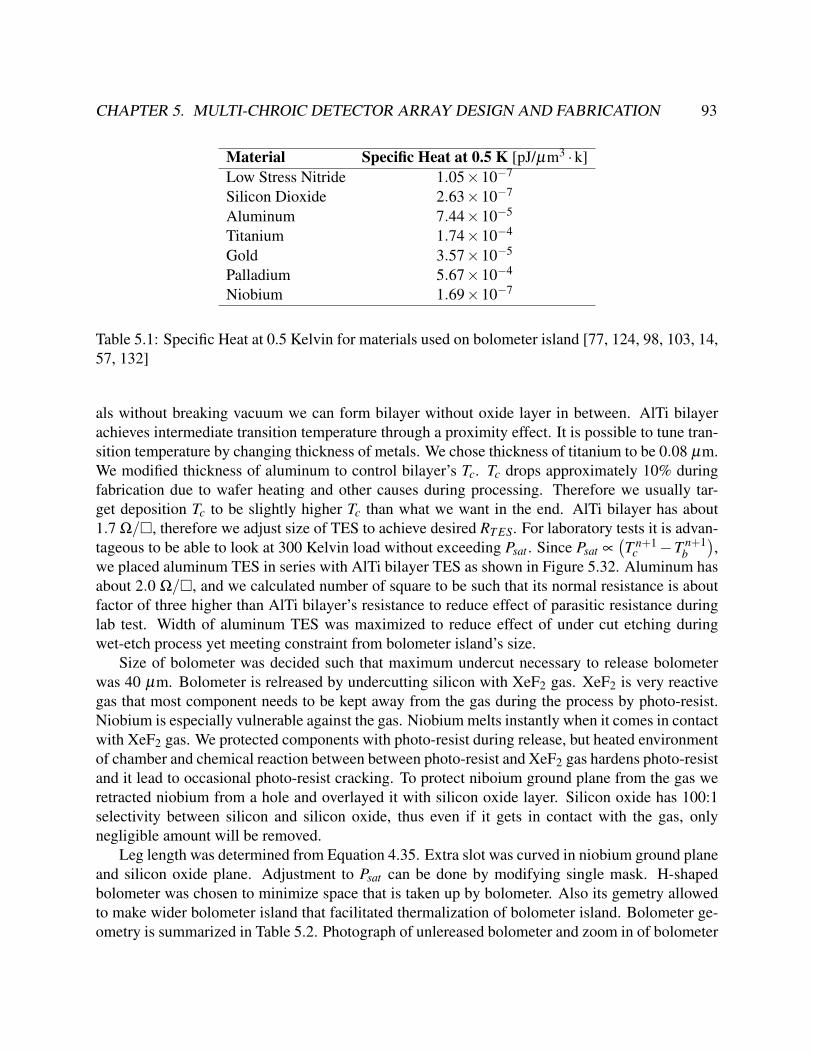
CHAPTER 5. MULTI-CHROIC DETECTOR ARRAY DESIGN AND FABRICATION 93
Material Specific Heat at 0.5 K [pJ/µm3 ·k]Low Stress Nitride 1.05×10⁻⁷
Silicon Dioxide 2.63×10⁻⁷
Aluminum 7.44×10⁻⁵
Titanium 1.74×10⁻⁴
Gold 3.57×10⁻⁵
Palladium 5.67×10⁻⁴
Niobium 1.69×10⁻⁷
Table 5.1: Specific Heat at 0.5 Kelvin for materials used on bolometer island [77, 124, 98, 103, 14,57, 132]
als without breaking vacuum we can form bilayer without oxide layer in between. AlTi bilayerachieves intermediate transition temperature through a proximity effect. It is possible to tune tran-sition temperature by changing thickness of metals. We chose thickness of titanium to be 0.08 µm.We modified thickness of aluminum to control bilayer’s Tc. Tc drops approximately 10% duringfabrication due to wafer heating and other causes during processing. Therefore we usually tar-get deposition Tc to be slightly higher Tc than what we want in the end. AlTi bilayer has about1.7 Ω/, therefore we adjust size of TES to achieve desired RT ES. For laboratory tests it is advan-tageous to be able to look at 300 Kelvin load without exceeding Psat . Since Psat ∝
(T n+1
c −T n+1b
),
we placed aluminum TES in series with AlTi bilayer TES as shown in Figure 5.32. Aluminum hasabout 2.0 Ω/, and we calculated number of square to be such that its normal resistance is aboutfactor of three higher than AlTi bilayer’s resistance to reduce effect of parasitic resistance duringlab test. Width of aluminum TES was maximized to reduce effect of under cut etching duringwet-etch process yet meeting constraint from bolometer island’s size.
Size of bolometer was decided such that maximum undercut necessary to release bolometerwas 40 µm. Bolometer is relreased by undercutting silicon with XeF2 gas. XeF2 is very reactivegas that most component needs to be kept away from the gas during the process by photo-resist.Niobium is especially vulnerable against the gas. Niobium melts instantly when it comes in contactwith XeF2 gas. We protected components with photo-resist during release, but heated environmentof chamber and chemical reaction between between photo-resist and XeF2 gas hardens photo-resistand it lead to occasional photo-resist cracking. To protect niboium ground plane from the gas weretracted niobium from a hole and overlayed it with silicon oxide layer. Silicon oxide has 100:1selectivity between silicon and silicon oxide, thus even if it gets in contact with the gas, onlynegligible amount will be removed.
Leg length was determined from Equation 4.35. Extra slot was curved in niobium ground planeand silicon oxide plane. Adjustment to Psat can be done by modifying single mask. H-shapedbolometer was chosen to minimize space that is taken up by bolometer. Also its gemetry allowedto make wider bolometer island that facilitated thermalization of bolometer island. Bolometer ge-ometry is summarized in Table 5.2. Photograph of unlereased bolometer and zoom in of bolometer
CHAPTER 5. MULTI-CHROIC DETECTOR ARRAY DESIGN AND FABRICATION 94
95 GHz 150 GHzLoad Resistor (AlTi) 4 4TES (AlTi) 0.88 1.12TES (Al) 2.25 2.85Bling 1 µm thick palladium 38 µm2 48 µm2
l 605 µm 357 µm
Table 5.2: Bolometer parameters
Figure 5.32: Microscope photograph of bolometer island (left) and bolometer (right). Dark back-ground around bolometer is due to cavity formed by XeF2 silicon etching.
island is shown in Figure 5.32.
5.8 EfficiencyTo estimate detector efficiency, we considered the AR coating efficiency, antenna forward gain loss,antenna impedance mismatch, impedance transformation, microstrip line dielectric loss, bandpassfilter efficiency, cross-over reflection and load resistor mismatch.
Instead of making optimized shaped anti-reflection coating, we form uniform thickness layeron lenslet. Loss from thickness mismatch after integrating over lenslet is 5%. Because antenna isfabricated on silicon-air dielectric half space, antenna preferentially accept power with efficiency of95%. Antenna mismatch is negligible, so we assume efficiency of 99%. Impedance transformationhappens smoothly over many wavelength, thus its reflection loss can be ignored. Microstrip linedielectric loss was also quoted as function of frequency assuming total length Ltotal = 14 mm.Since we do not know exact value of loss-tangent for our dielectric, we graphed range of efficiencywith tan(δ ) from 1×10⁻³ to 7×10⁻³. tan(δ ) in silicon dioxide could vary between 1×10⁻³ to7×10−3 depending on deposition conditions [74]. Bandpass filter efficiency was also simulated byentering dielectric loss into simulation. In-band efficiency range for various loss tangent values are
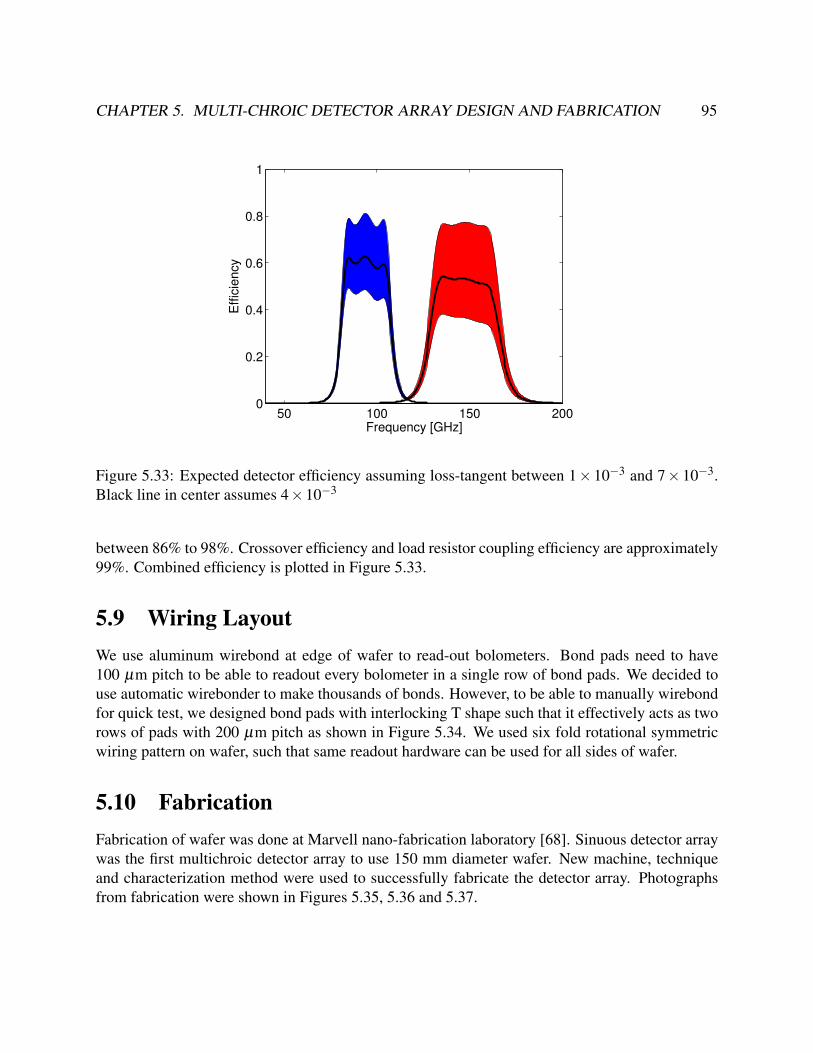
CHAPTER 5. MULTI-CHROIC DETECTOR ARRAY DESIGN AND FABRICATION 95
50 100 150 2000
0.2
0.4
0.6
0.8
1
Frequency [GHz]
Effic
iency
Figure 5.33: Expected detector efficiency assuming loss-tangent between 1×10⁻³ and 7×10⁻³.Black line in center assumes 4×10⁻³
between 86% to 98%. Crossover efficiency and load resistor coupling efficiency are approximately99%. Combined efficiency is plotted in Figure 5.33.
5.9 Wiring LayoutWe use aluminum wirebond at edge of wafer to read-out bolometers. Bond pads need to have100 µm pitch to be able to readout every bolometer in a single row of bond pads. We decided touse automatic wirebonder to make thousands of bonds. However, to be able to manually wirebondfor quick test, we designed bond pads with interlocking T shape such that it effectively acts as tworows of pads with 200 µm pitch as shown in Figure 5.34. We used six fold rotational symmetricwiring pattern on wafer, such that same readout hardware can be used for all sides of wafer.
5.10 FabricationFabrication of wafer was done at Marvell nano-fabrication laboratory [68]. Sinuous detector arraywas the first multichroic detector array to use 150 mm diameter wafer. New machine, techniqueand characterization method were used to successfully fabricate the detector array. Photographsfrom fabrication were shown in Figures 5.35, 5.36 and 5.37.
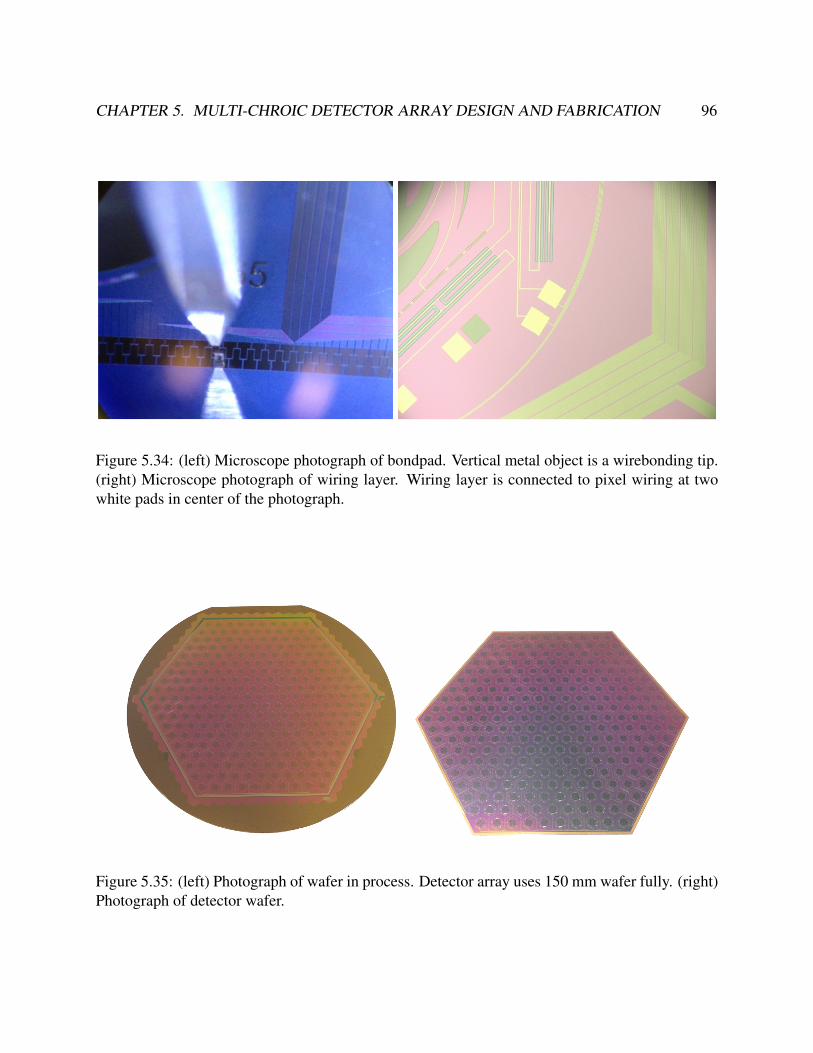
CHAPTER 5. MULTI-CHROIC DETECTOR ARRAY DESIGN AND FABRICATION 96
Figure 5.34: (left) Microscope photograph of bondpad. Vertical metal object is a wirebonding tip.(right) Microscope photograph of wiring layer. Wiring layer is connected to pixel wiring at twowhite pads in center of the photograph.
Figure 5.35: (left) Photograph of wafer in process. Detector array uses 150 mm wafer fully. (right)Photograph of detector wafer.
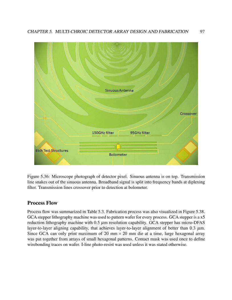
CHAPTER 5. MULTI-CHROIC DETECTOR ARRAY DESIGN AND FABRICATION 97
Figure 5.36: Microscope photograph of detector pixel. Sinuous antenna is on top. Transmissionline snakes out of the sinuous antenna. Broadband signal is split into frequency bands at diplexingfilter. Transmission lines crossover prior to detection at bolometer.
Process FlowProcess flow was summarized in Table 5.3. Fabrication process was also visualized in Figure 5.38.GCA stepper lithography machine was used to pattern wafer for every process. GCA stepper is a x5reduction lithography machine with 0.5 µm resolution capability. GCA stepper has micro-DFASlayer-to-layer aligning capability, that achieves layer-to-layer alignment of better than 0.3 µm.Since GCA can only print maximum of 20 mm× 20 mm die at a time, large hexagonal arraywas put together from arrays of small hexagonal patterns. Contact mask was used once to definewirebonding traces on wafer. I-line photo-resist was used unless it was stated otherwise.
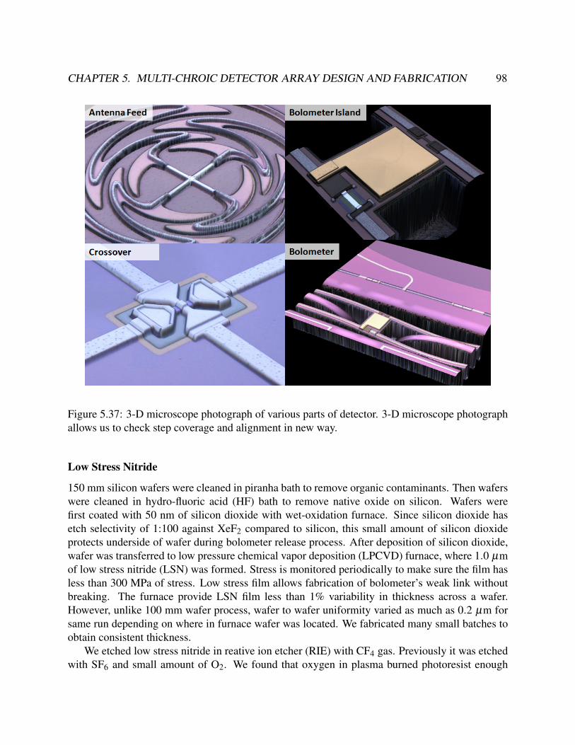
CHAPTER 5. MULTI-CHROIC DETECTOR ARRAY DESIGN AND FABRICATION 98
Figure 5.37: 3-D microscope photograph of various parts of detector. 3-D microscope photographallows us to check step coverage and alignment in new way.
Low Stress Nitride
150 mm silicon wafers were cleaned in piranha bath to remove organic contaminants. Then waferswere cleaned in hydro-fluoric acid (HF) bath to remove native oxide on silicon. Wafers werefirst coated with 50 nm of silicon dioxide with wet-oxidation furnace. Since silicon dioxide hasetch selectivity of 1:100 against XeF2 compared to silicon, this small amount of silicon dioxideprotects underside of wafer during bolometer release process. After deposition of silicon dioxide,wafer was transferred to low pressure chemical vapor deposition (LPCVD) furnace, where 1.0 µmof low stress nitride (LSN) was formed. Stress is monitored periodically to make sure the film hasless than 300 MPa of stress. Low stress film allows fabrication of bolometer’s weak link withoutbreaking. The furnace provide LSN film less than 1% variability in thickness across a wafer.However, unlike 100 mm wafer process, wafer to wafer uniformity varied as much as 0.2 µm forsame run depending on where in furnace wafer was located. We fabricated many small batches toobtain consistent thickness.
We etched low stress nitride in reative ion etcher (RIE) with CF4 gas. Previously it was etchedwith SF6 and small amount of O2. We found that oxygen in plasma burned photoresist enough

CHAPTER 5. MULTI-CHROIC DETECTOR ARRAY DESIGN AND FABRICATION 99
Figure 5.38: Step by step cross-section of fabrication. Step number corresponds to step ID inTable 5.3
during the process. Niobium was exposed as a result, and niobium was destroyed by XeF2 gasin the following release process. We looked for alternative gas that etches LSN without burningphoto-resist. We had successful fabrication with CF4 plasma etch on LSN.
Niobium
Niobium was put down by DC Magnetron sputter machine. Chamber pressure during depositionwas adjusted to 3 mTorr to control film stress. Machine was originally designed for 100 mm wafer.So we designed new 150 mm diameter chuck, and we tested film uniformity. The machine has arotating magnet that modulates plasma during deposition to make deposition more uniform. Evenwith the rotating magnet, there was 10% difference in relative thickness radially across wafer withcenter being thicker.
We experimented with two different machines for niobium etch. First machine was a reactiveion etcher, RIE system 1000 TP, from the SEMI group. The machine has a 12 inch chuck that has
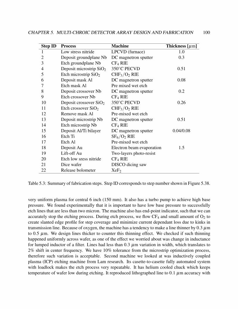
CHAPTER 5. MULTI-CHROIC DETECTOR ARRAY DESIGN AND FABRICATION 100
Step ID Process Machine Thickness [µm]1 Low stress nitride LPCVD (furnace) 1.02 Deposit groundplane Nb DC magnetron sputter 0.33 Etch groundplane Nb CF4 RIE4 Deposit microstrip SiO2 350C PECVD 0.515 Etch microstrip SiO2 CHF3/O2 RIE6 Deposit mask Al DC magnetron sputter 0.087 Etch mask Al Pre mixed wet etch8 Deposit crossover Nb DC magnetron sputter 0.29 Etch crossover Nb CF4 RIE10 Deposit crossover SiO2 350C PECVD 0.2611 Etch crossover SiO2 CHF3/O2 RIE12 Remove mask Al Pre-mixed wet etch13 Deposit microstrip Nb DC magnetron sputter 0.5114 Etch microstrip Nb CF4 RIE15 Deposit Al/Ti bilayer DC magnetron sputter 0.04/0.0816 Etch Ti SF6/O2 RIE17 Etch Al Pre-mixed wet etch18 Deposit Au Electron beam evaporation 1.519 Lift-off Au Two-layers photo-resist20 Etch low sress nitride CF4 RIE21 Dice wafer DISCO dicing saw22 Release bolometer XeF2
Table 5.3: Summary of fabrication steps. Step ID corresponds to step number shown in Figure 5.38.
very uniform plasma for central 6 inch (150 mm). It also has a turbo pump to achieve high basepressure. We found experimentally that it is important to have low base pressure to successfullyetch lines that are less than two micron. The machine also has end-point indicator, such that we canaccurately stop the etching process. During etch process, we flow CF4 and small amount of O2 tocreate slanted edge profile for step coverage and minimize current dependant loss due to kinks intransmission line. Because of oxygen, the machine has a tendency to make a line thinner by 0.3 µmto 0.5 µm. We design lines thicker to counter this thinning effect. We checked if such thinninghappened uniformly across wafer, as one of the effect we worried about was change in inductancefor lumped inductor of a filter. Lines had less than 0.3 µm variation in width, which translates to2% shift in center frequency. We have 10% tolerance from the microstrip optimization process,therefore such variation is acceptable. Second machine we looked at was inductively coupledplasma (ICP) etching machine from Lam research. Its casette-to-casette fully automated systemwith loadlock makes the etch process very repeatable. It has helium cooled chuck which keepstemperature of wafer low during etching. It reproduced lithographed line to 0.1 µm accuracy with
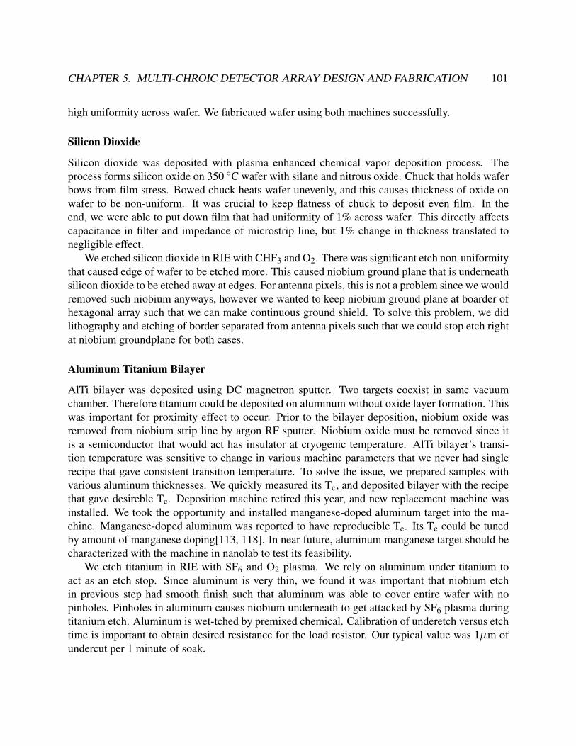
CHAPTER 5. MULTI-CHROIC DETECTOR ARRAY DESIGN AND FABRICATION 101
high uniformity across wafer. We fabricated wafer using both machines successfully.
Silicon Dioxide
Silicon dioxide was deposited with plasma enhanced chemical vapor deposition process. Theprocess forms silicon oxide on 350 C wafer with silane and nitrous oxide. Chuck that holds waferbows from film stress. Bowed chuck heats wafer unevenly, and this causes thickness of oxide onwafer to be non-uniform. It was crucial to keep flatness of chuck to deposit even film. In theend, we were able to put down film that had uniformity of 1% across wafer. This directly affectscapacitance in filter and impedance of microstrip line, but 1% change in thickness translated tonegligible effect.
We etched silicon dioxide in RIE with CHF3 and O2. There was significant etch non-uniformitythat caused edge of wafer to be etched more. This caused niobium ground plane that is underneathsilicon dioxide to be etched away at edges. For antenna pixels, this is not a problem since we wouldremoved such niobium anyways, however we wanted to keep niobium ground plane at boarder ofhexagonal array such that we can make continuous ground shield. To solve this problem, we didlithography and etching of border separated from antenna pixels such that we could stop etch rightat niobium groundplane for both cases.
Aluminum Titanium Bilayer
AlTi bilayer was deposited using DC magnetron sputter. Two targets coexist in same vacuumchamber. Therefore titanium could be deposited on aluminum without oxide layer formation. Thiswas important for proximity effect to occur. Prior to the bilayer deposition, niobium oxide wasremoved from niobium strip line by argon RF sputter. Niobium oxide must be removed since itis a semiconductor that would act has insulator at cryogenic temperature. AlTi bilayer’s transi-tion temperature was sensitive to change in various machine parameters that we never had singlerecipe that gave consistent transition temperature. To solve the issue, we prepared samples withvarious aluminum thicknesses. We quickly measured its Tc, and deposited bilayer with the recipethat gave desireble Tc. Deposition machine retired this year, and new replacement machine wasinstalled. We took the opportunity and installed manganese-doped aluminum target into the ma-chine. Manganese-doped aluminum was reported to have reproducible Tc. Its Tc could be tunedby amount of manganese doping[113, 118]. In near future, aluminum manganese target should becharacterized with the machine in nanolab to test its feasibility.
We etch titanium in RIE with SF6 and O2 plasma. We rely on aluminum under titanium toact as an etch stop. Since aluminum is very thin, we found it was important that niobium etchin previous step had smooth finish such that aluminum was able to cover entire wafer with nopinholes. Pinholes in aluminum causes niobium underneath to get attacked by SF6 plasma duringtitanium etch. Aluminum is wet-tched by premixed chemical. Calibration of underetch versus etchtime is important to obtain desired resistance for the load resistor. Our typical value was 1µm ofundercut per 1 minute of soak.
CHAPTER 5. MULTI-CHROIC DETECTOR ARRAY DESIGN AND FABRICATION 102
Gold
Since gold cannot be plasma etched, we use photo-resist lift off process to pattern gold. We createoverhang structure by using two different kinds of photo-resist. First we deposit 2 µm of G-linephoto-resist, then we deposit 1.2 µm of I-line photo-resist. After a wafer is lithographed, wedevelopped the wafer with developper for I-line resist. This will create accurate pattern on I-line,but it will undercut G-line resist. Thus there will be overhung structure. This allows gold thatwould be left behind to not be in physical contact with photo-resist. Also it creates a window foracetone to get underneath gold to remove photo-resist away. We deposit gold using electron beamevaporator. Power of electron gun is kept low to prevent photo-resist on wafer from burning ontowafer. Deposition thus takes few hours. For future fabrication, we would like to increase timeconstant of bolometer. To obtain enough heat capacitance while keeping volume of bling small,we explored palladium that is known to have higher heat capacitance than gold [103]. Evaporationof palladium requires higher temperature than gold, so deposition rate and condition of photo-resistafter evaporation needs to be evaluated in future fabrication.
Crossover
Aluminum mask was used for fabrication of a crossover. Prior to making the crossover on a wafer,LSN, niobium groundplane and silicon dioxide for microstrip line is layed down on a wafer. Wedid not want to have etch on niobium layer for crossover to stop on the silicon dioxide as that wouldreduce the thickness of silicon dioxide slightly. To solve the problem, we masked most of waferwith aluminum such that niobium etch would stop on aluminum. Aluminum does not get etchedwith fluorine plasma used for niobium etch. We left window in aluminum that is just big enoughto form crossover as shown in Figure 5.37. Aluminum wet etches away cleanly after crossover isformed in the window.
Bolometer Release
Bolometer island is released by removing silicon underneath the bolometer with XeF2 gas. Sincereleased bolometer will be fragile, we dice wafer into hexagonal shape prior to the release. Waferis dried in an oven since HF forms when water molecule reacts with XeF2 gas which would thendestroy structures on wafer [11]. During etch, we monitor its progress and uniformity using releasestructure shown in Figreu 5.39. Test structure has identical dimension as actual bolometer island.Niobium ground plane is removed at the test structure, such that it is possible to see throughsilicon oxide and silicon nitride to monitor how much silicon is left under the bolometer island.Rectangular section left in middle of bolometer island as shown in Figure 5.39 is portion of siliconthat is not removed yet. Using such structure, we were able to accurately tell end point and releaseuniformity. Uniformity across wafer is ±5 µm. It is negligible error compared to total bolometerleg-length l.
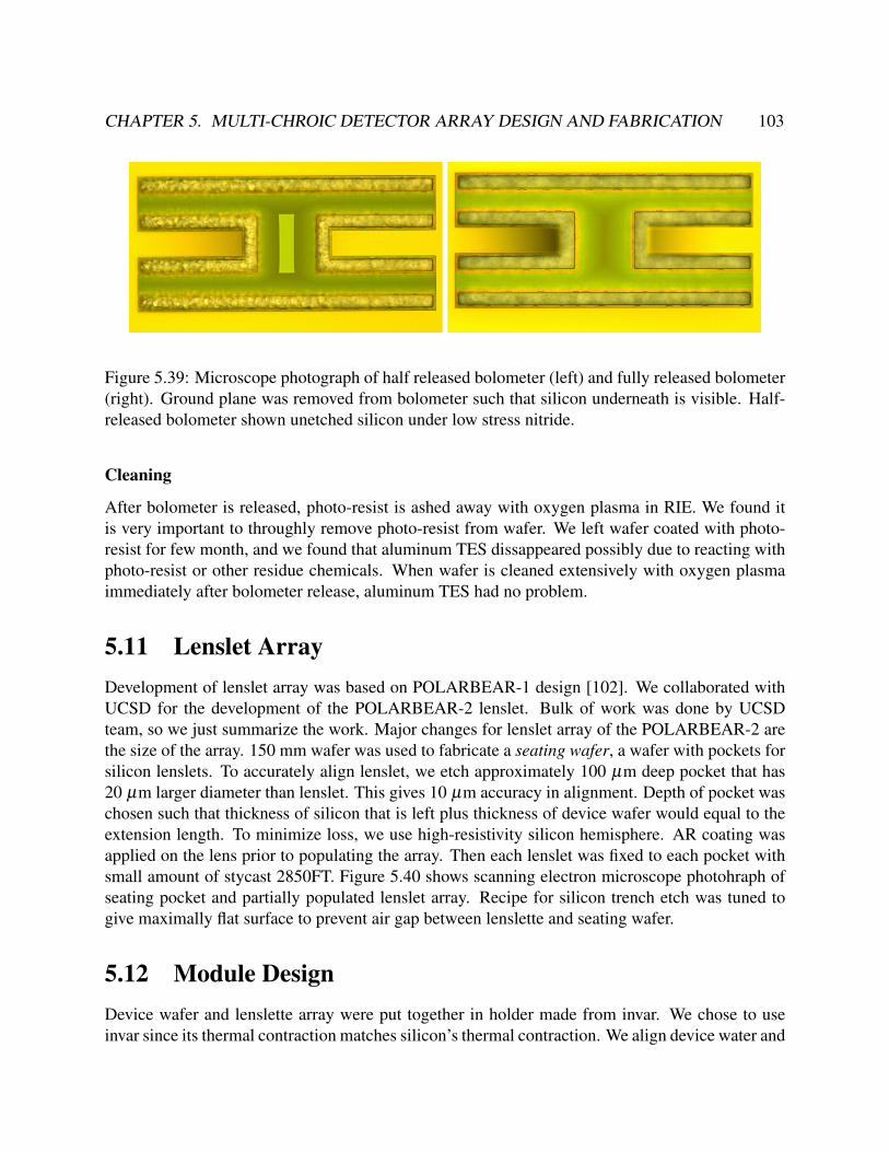
CHAPTER 5. MULTI-CHROIC DETECTOR ARRAY DESIGN AND FABRICATION 103
Figure 5.39: Microscope photograph of half released bolometer (left) and fully released bolometer(right). Ground plane was removed from bolometer such that silicon underneath is visible. Half-released bolometer shown unetched silicon under low stress nitride.
Cleaning
After bolometer is released, photo-resist is ashed away with oxygen plasma in RIE. We found itis very important to throughly remove photo-resist from wafer. We left wafer coated with photo-resist for few month, and we found that aluminum TES dissappeared possibly due to reacting withphoto-resist or other residue chemicals. When wafer is cleaned extensively with oxygen plasmaimmediately after bolometer release, aluminum TES had no problem.
5.11 Lenslet ArrayDevelopment of lenslet array was based on POLARBEAR-1 design [102]. We collaborated withUCSD for the development of the POLARBEAR-2 lenslet. Bulk of work was done by UCSDteam, so we just summarize the work. Major changes for lenslet array of the POLARBEAR-2 arethe size of the array. 150 mm wafer was used to fabricate a seating wafer, a wafer with pockets forsilicon lenslets. To accurately align lenslet, we etch approximately 100 µm deep pocket that has20 µm larger diameter than lenslet. This gives 10 µm accuracy in alignment. Depth of pocket waschosen such that thickness of silicon that is left plus thickness of device wafer would equal to theextension length. To minimize loss, we use high-resistivity silicon hemisphere. AR coating wasapplied on the lens prior to populating the array. Then each lenslet was fixed to each pocket withsmall amount of stycast 2850FT. Figure 5.40 shows scanning electron microscope photohraph ofseating pocket and partially populated lenslet array. Recipe for silicon trench etch was tuned togive maximally flat surface to prevent air gap between lenslette and seating wafer.
5.12 Module DesignDevice wafer and lenslette array were put together in holder made from invar. We chose to useinvar since its thermal contraction matches silicon’s thermal contraction. We align device water and

CHAPTER 5. MULTI-CHROIC DETECTOR ARRAY DESIGN AND FABRICATION 104
Figure 5.40: (left) SEM photograph of seating wafer cross section. (right) Photograph of partiallypopulated lenslet array. Cortesy of Praween Siritanasak
lenslette array using infrared optical microscope as shwon in Figure 5.41. Wafer was illuminatedfrom bottom with halogen lamp. Infrared from halogen lamp transmit through silicon, but infraredlight get blocked by niobium. We etch slot in niobium to let some light through, and transmittedinfrared light is captured by CCD. At the same time, optical image of seating wafer is capturedfrom top. Thus we can overlay two images to align two wafers together. We etched 40 µm wideslot into niobium and seating wafer. As shwon in Figure 5.41, we consistently aligned device waferto lenslette to 10 µm accuracy. We thermal cycled aligned wafer many times, and we verified thatwafers stay aligned.
Invar holderDesign for POLARBEAR-2’s invar holder was based on POLARBEAR-1’s design [60]. We col-laborated with KEK to develop invar holder for the POLARBEAR-2. Since invar holder holdswafers that are very brittle, we worried about its flatness. Invar was heat treated to remove itsstress prior to machining. Machining was then done carefully to not apply stress into material.As shown in Figure 5.42 and 5.48, structure has large opening. Since the holder is twice as big indiameter as POLARBEAR-1 design, we made invar holder about twice as thick to keep its flatness.Thick holder also helps to give extra room behind antenna which turned out to be important forbeam synthesis.
BackshortWirebond pads on device wafers are placed at the edge of wafer. Initially we considered wire-bonding directly to a bondpad at a pixel from behind. To test this idea, we made printed circuit
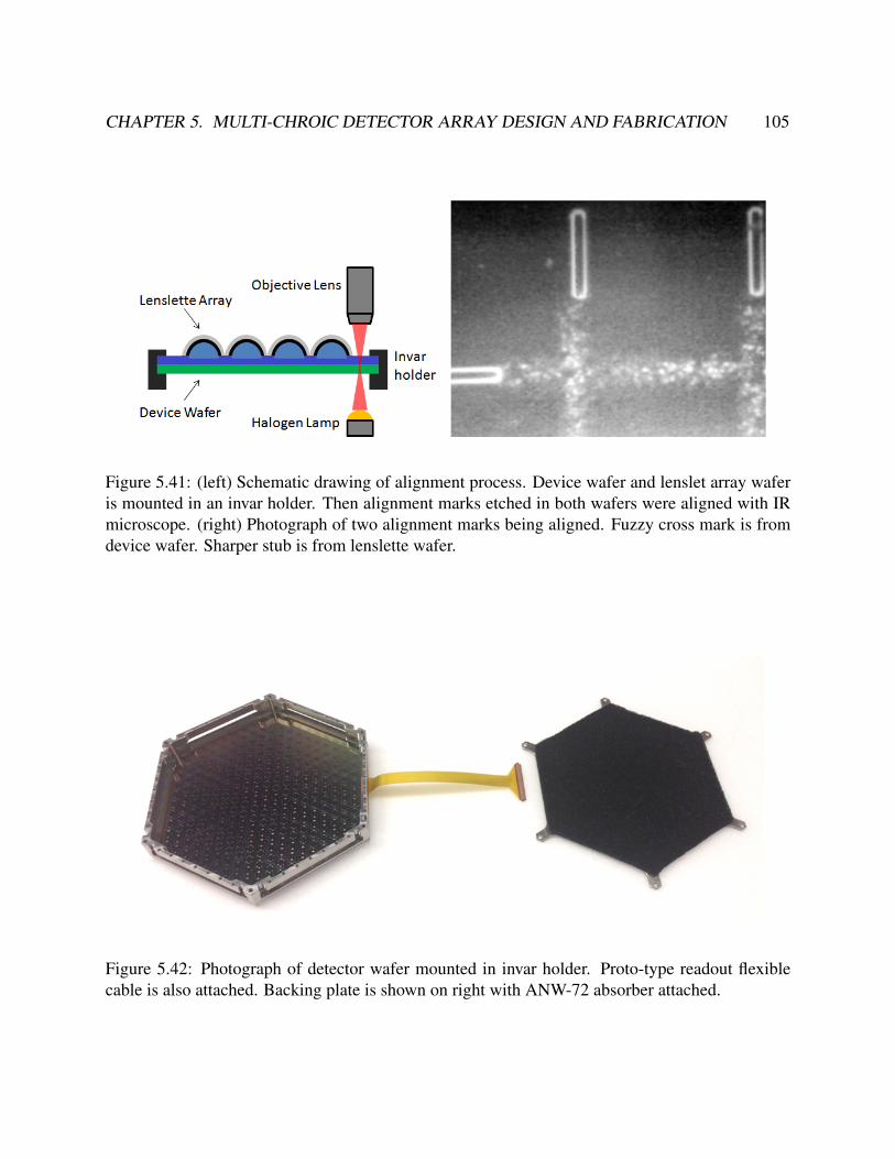
CHAPTER 5. MULTI-CHROIC DETECTOR ARRAY DESIGN AND FABRICATION 105
Figure 5.41: (left) Schematic drawing of alignment process. Device wafer and lenslet array waferis mounted in an invar holder. Then alignment marks etched in both wafers were aligned with IRmicroscope. (right) Photograph of two alignment marks being aligned. Fuzzy cross mark is fromdevice wafer. Sharper stub is from lenslette wafer.
Figure 5.42: Photograph of detector wafer mounted in invar holder. Proto-type readout flexiblecable is also attached. Backing plate is shown on right with ANW-72 absorber attached.

CHAPTER 5. MULTI-CHROIC DETECTOR ARRAY DESIGN AND FABRICATION 106
Figure 5.43: Schematic drawing of absorber test setup.
Absorber TE reflectivity on aluminum at 150 GHzLoaded epoxy ≈ 20%HR-10 < 3%ANW-72 5%−15%
Table 5.4: Reflection of absorbers at 150 GHz [120].
board structure that hovered behind pixel. Then we wirebonded from the printed circuit boardto a test pixel. Since printed circuit board has metal traces we thought it would be good idea toapply absorber on surface as shown in Figure 5.43. First we applied stycast 2850FT loaded with175 µm diameter glass beads and carbon powder [18]. It gave distorted beam as shown in Fig-ure 5.44. We then realized such loaded epoxy was excellent infrared absorber, but it is not anabsorber at 150 GHz as shown in Table 5.4 [120]. According to the table, HR-10 would be thebest material, but HR-10 is very fragile and porous to be used in tight space. Thus we removedloaded epoxy from the printed circuit board and re-coated it with ANW-72. We measured roundbeam with ANW-72 coating. We did not end up using this 3-D readout scheme. This exercize gaveus important information that we need to terminate antenna’s backlobe with good absorber. ThePOLARBEAR-2 decided to use ANW-72 to better terminate antenna’s backlobe for a better beamshape.
5.13 Readout Component FabricationWe use frequency multiplexing to readout 36 bolometers per SQUID. Key components are induc-tors and capacitors that defines frequency of the readout. As we discussed in Section 4.6, we wantto minimize loss in capacitor to minimize parasitic resistance in capacitor. We fabricated inter-digitated capacitor on high-resistivity silicon that is reported to have loss-tangent of 2× 10⁻⁴ at
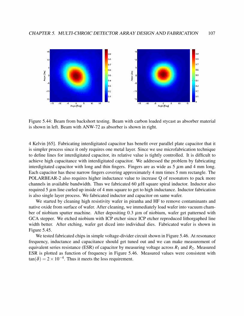
CHAPTER 5. MULTI-CHROIC DETECTOR ARRAY DESIGN AND FABRICATION 107
Figure 5.44: Beam from backshort testing. Beam with carbon loaded stycast as absorber materialis shown in left. Beam with ANW-72 as absorber is shown in right.
4 Kelvin [65]. Fabricating interdigitated capacitor has benefit over parallel plate capacitor that itis simpler process since it only requires one metal layer. Since we use microfabrication techniqueto define lines for interdigitated capacitor, its relative value is tightly controlled. It is difficult toachieve high capacitance with interdigitated capacitor. We addressed the problem by fabricatinginterdigitated capacitor with long and thin fingers. Fingers are as wide as 5 µm and 4 mm long.Each capacitor has these narrow fingers covering approximately 4 mm times 5 mm rectangle. ThePOLARBEAR-2 also requires higher inductance value to increase Q of resonators to pack morechannels in available bandwidth. Thus we fabricated 60 µH square spiral inductor. Inductor alsorequired 5 µm line curled up inside of 4 mm square to get to high inductance. Inductor fabricationis also single layer process. We fabricated inductor and capacitor on same wafer.
We started by cleaning high resistivity wafer in piranha and HF to remove contaminants andnative oxide from surface of wafer. After cleaning, we immediately load wafer into vacuum cham-ber of niobium sputter machine. After depositing 0.3 µm of niobium, wafer get patterned withGCA stepper. We etched niobium with ICP etcher since ICP etcher reproduced lithorgaphed linewidth better. After etching, wafer get diced into individual dies. Fabricated wafer is shown inFigure 5.45.
We tested fabricated chips in simple voltage-divider circuit shown in Figure 5.46. At resonancefrequency, inductance and capacitance should get tuned out and we can make measurement ofequivalent series resistance (ESR) of capacitor by measuring voltage across R1 and R2. MeasuredESR is plotted as function of frequency in Figure 5.46. Measured values were consistent withtan(δ ) = 2×10⁻⁴. Thus it meets the loss requirement.

CHAPTER 5. MULTI-CHROIC DETECTOR ARRAY DESIGN AND FABRICATION 108
Figure 5.45: Photograph of wafer with interdigitated capacitor and inductors. Zoomed in micro-scope photograph is shown on right
Figure 5.46: (left) Circuit diagram for ESR testing (right) Result from ESR testing is shown onright. Loss from interdigitated capacitor fabricated on high resistivity silicon is lower.
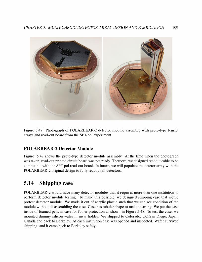
CHAPTER 5. MULTI-CHROIC DETECTOR ARRAY DESIGN AND FABRICATION 109
Figure 5.47: Photograph of POLARBEAR-2 detector module assembly with proto-type lensletarrays and read-out board from the SPT-pol experiment
POLARBEAR-2 Detector ModuleFigure 5.47 shows the proto-type detector module assembly. At the time when the photographwas taken, read-out printed circuit board was not ready. Thereore, we designed readout cable to becompatible with the SPT-pol read-out board. In future, we will populate the detetor array with thePOLARBEAR-2 original design to fully readout all detectors.
5.14 Shipping casePOLARBEAR-2 would have many detector modules that it requires more than one institution toperform detector module testing. To make this possible, we designed shipping case that wouldprotect detector module. We made it out of acrylic plastic such that we can see condition of themodule without disassembling the case. Case has tubuler shape to make it strong. We put the caseinside of foamed pelican case for futher protection as shown in Figure 5.48. To test the case, wemounted dummy silicon wafer in invar holder. We shipped to Colorado, UC San Diego, Japan,Canada and back to Berkeley. At each institution case was opened and inspected. Wafer survivedshipping, and it came back to Berkeley safely.
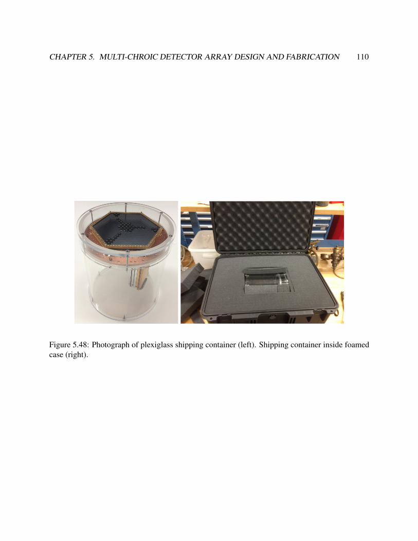
CHAPTER 5. MULTI-CHROIC DETECTOR ARRAY DESIGN AND FABRICATION 110
Figure 5.48: Photograph of plexiglass shipping container (left). Shipping container inside foamedcase (right).
111
Chapter 6
Detector Characterization
6.1 IntroductionWe describe detector characterization in this chapter. We will discuss how test apparatus weredesigned and used. We will then discuss results from measurements.
6.2 DewarOur detectors are designed to operate at 250 milli-Kelvin. Dewars were designed to transmitmillimeter wave into dewar while meeting thermal requirement by cutting down thermal loadingfrom infrared. In this section we will describe two dewars we used for testing.
8 inch IR-Lab DewarWe tested the prototype pixels in an 8 inch IR Labs dewar. Dewar of this size was useful forprototype testing since it only takes eight hours to reach milli-Kelvin temperature from room tem-perature. We modified the dewar by adding a 4 inch diameter optical window made from ZotefoamPPA30. For infrared filters, two layers of 0.125 inch thick expanded teflon and a metal mesh lowpass filter with 18 cm−1 cut off are anchored to a liquid nitrogen temperature [126]. Two metalmesh low pass filters with cut off at 14 cm−1 and 12 cm−1 are mounted at liquid helium bufferto further reduce the optical loading. The milli-kelvin stage is isolated from the liquid heliumbuffer with thin walled vespel tubes. The stage is cooled to 250 milli-Kelvin with homemade 3Headsorption fridge. Cross section of dewar is shown in Figure 6.1.
Readout Electronics
Bias voltage for bolometer was provided by simple circit shown in Figure 6.2. Small shunt resistorwith 0.02 Ω that is parallel to a bolometer with typical resistance of 1 Ω provides voltage bias on abolometer. We create voltage divider with 2K Ω room temperature resistor and 0.02 Ω bias resistor,
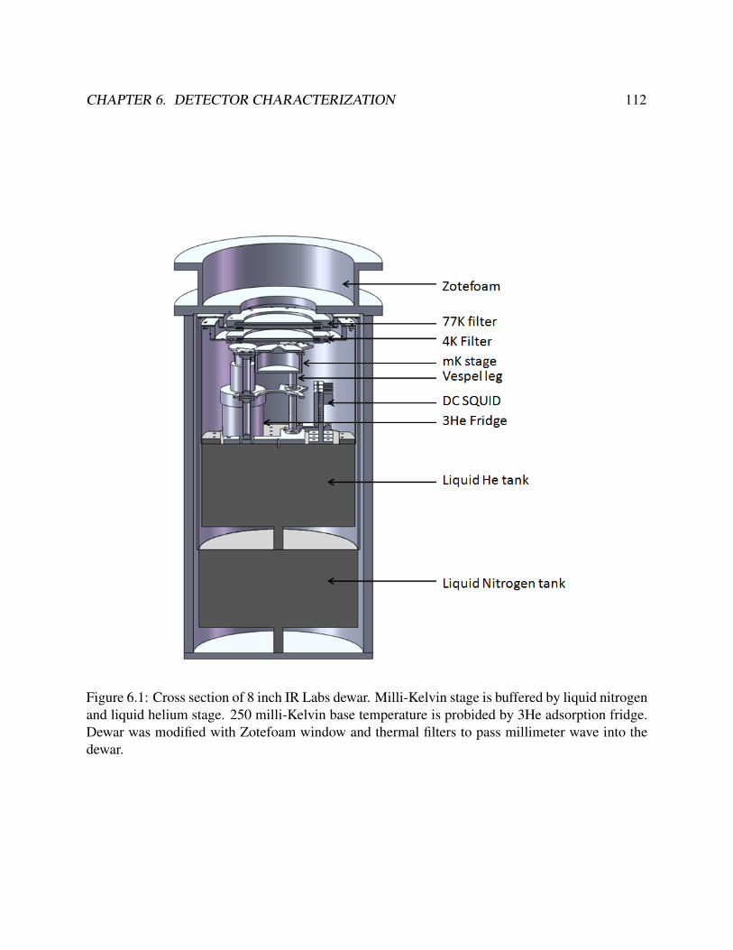
CHAPTER 6. DETECTOR CHARACTERIZATION 112
Figure 6.1: Cross section of 8 inch IR Labs dewar. Milli-Kelvin stage is buffered by liquid nitrogenand liquid helium stage. 250 milli-Kelvin base temperature is probided by 3He adsorption fridge.Dewar was modified with Zotefoam window and thermal filters to pass millimeter wave into thedewar.

CHAPTER 6. DETECTOR CHARACTERIZATION 113
Figure 6.2: Circuit diagram for readout electronics. Colors separate circuit at different tempera-tures.
thus we can monitor bias voltage across bolometer by looking at voltage across 2K Ω resistor andmultiply by 10−5. Current through the bolometer is read out by commercially available laboratoryDC SQUID from Quantum Design with its input inductor coil in series with the bolometer [101].It is important to use superconducting line beyond bias resistor to keep voltage bias on bolometer.
Large lens test
We performed initial tests with a 14 mm diameter lens. Large lens was useful since it producednarrower beam that was easier to couple to test apparatus. For tests with a large lens, we mountedthe test pixel behind the 14 mm diameter hemispherical silicon lens with 2.5 mm thick flat sili-con spacer. The test pixel was fabricated on top of 0.675 mm thick silicon, thus combination ofspacer and the test pixel locate the antenna at the elliptical focus. Test chip was aligned to spacerunder microscope. Test chip and spacer were fixed to each other by GE varnish. We appliedthermoformed quarter wavelength thick Ultem-1000 plastic on the lens for an AR coating. It getsmounted on circular copper plate on milli-Kelvin stage, and pixel is enclosed by copper can withANW-72 absorber inside as shown in Figure 6.3.
Lenslette array test
We then tested with lens size that is similar to what we would use in the field. For detector tests withsmaller lenses, we fabricated three different sizes of wafers as shown in Figure 6.4. We fabricatedthe POLARBEAR-2 size, the POLARBEAR-1 size and two pixel sinuous detector arrays. Pixelspacing and size of the POLARBEAR-1 size sinuous wafer was same as the POLARBEAR-1detector array, therefore we were able to use the POLARBEAR-1 spare lenslet array and invarholder to test sinuous detector with smaller lens. Milli-Kelvin stage was modified to accomodate
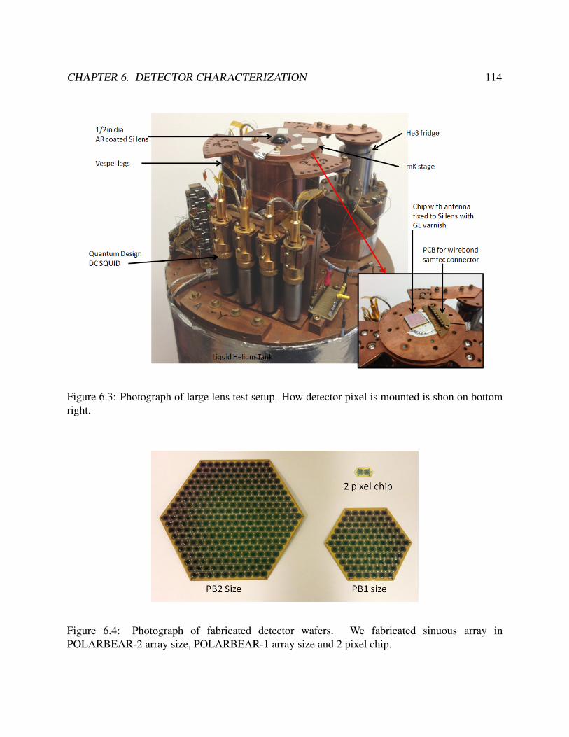
CHAPTER 6. DETECTOR CHARACTERIZATION 114
Figure 6.3: Photograph of large lens test setup. How detector pixel is mounted is shon on bottomright.
Figure 6.4: Photograph of fabricated detector wafers. We fabricated sinuous array inPOLARBEAR-2 array size, POLARBEAR-1 array size and 2 pixel chip.
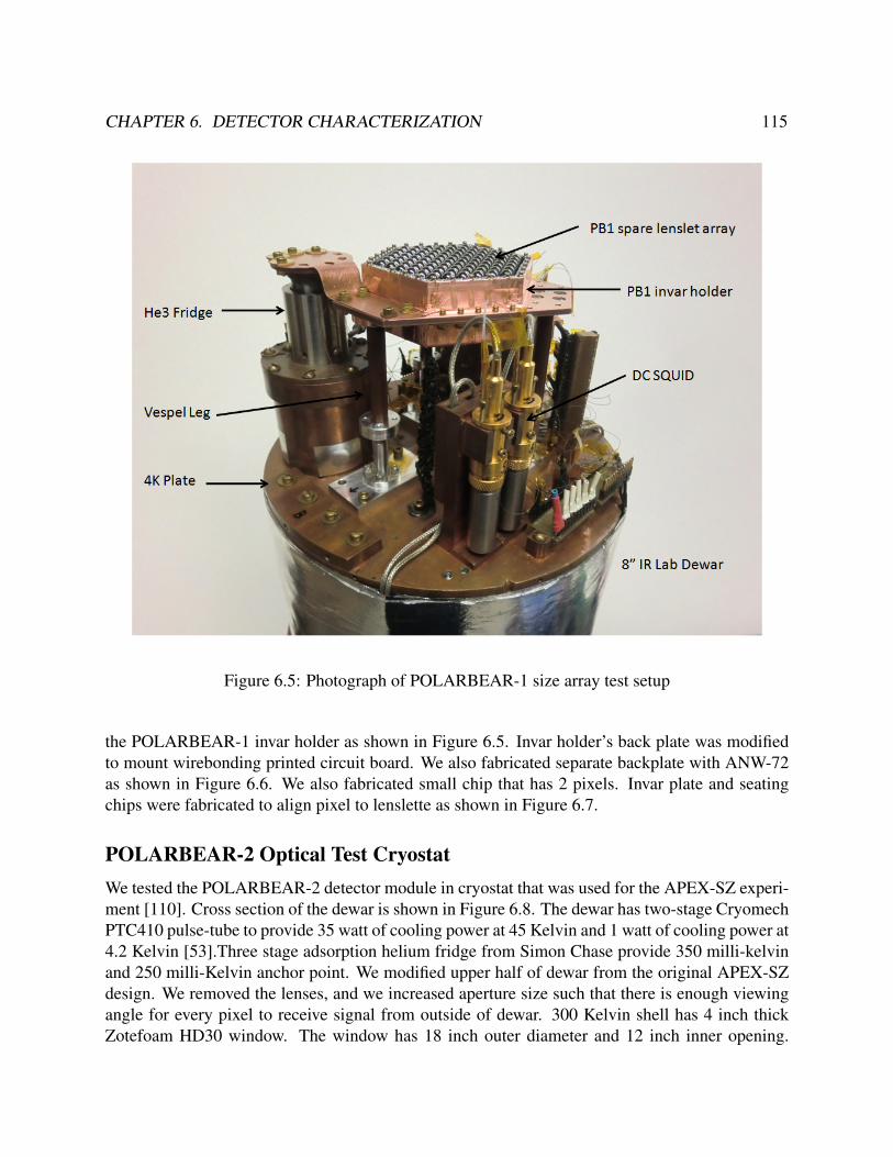
CHAPTER 6. DETECTOR CHARACTERIZATION 115
Figure 6.5: Photograph of POLARBEAR-1 size array test setup
the POLARBEAR-1 invar holder as shown in Figure 6.5. Invar holder’s back plate was modifiedto mount wirebonding printed circuit board. We also fabricated separate backplate with ANW-72as shown in Figure 6.6. We also fabricated small chip that has 2 pixels. Invar plate and seatingchips were fabricated to align pixel to lenslette as shown in Figure 6.7.
POLARBEAR-2 Optical Test CryostatWe tested the POLARBEAR-2 detector module in cryostat that was used for the APEX-SZ experi-ment [110]. Cross section of the dewar is shown in Figure 6.8. The dewar has two-stage CryomechPTC410 pulse-tube to provide 35 watt of cooling power at 45 Kelvin and 1 watt of cooling power at4.2 Kelvin [53].Three stage adsorption helium fridge from Simon Chase provide 350 milli-kelvinand 250 milli-Kelvin anchor point. We modified upper half of dewar from the original APEX-SZdesign. We removed the lenses, and we increased aperture size such that there is enough viewingangle for every pixel to receive signal from outside of dewar. 300 Kelvin shell has 4 inch thickZotefoam HD30 window. The window has 18 inch outer diameter and 12 inch inner opening.

CHAPTER 6. DETECTOR CHARACTERIZATION 116
Figure 6.6: Photograph of POLARBEAR-1 size sinuous array mounted on invar holder. ANW-72backabsorber terminates backlobe of antenna. Setup required long wirebond as shown in bottomright of the picture.
1 inch thick and 12 inch diameter teflon disk absorbs infrared radiation at 50 Kelvin stage. Ametal mesh low pass filter with 10 cm−1 cut off are also anchored to the 50 Kelvin shell behindteflon. Four metal mesh low pass filters with cut off at 19 cm−1, 15 cm−1, 8.5 cm−1 and 5.7 cm−1
are anchored to 4 Kelvin shell. Finally metal mesh filter with cut off at 6.5 cm−1 is anchored at0.35 Kelvin stage. Detector module is mounted on copper plate, and the copper plate is bolted onto250 milli-Kelvin stage as shown in Figure 6.9.
Readout Electronics
Readout for detector module uses frequency multiplexing system. The circuit diagram is shown inFigure 6.10. For detector module test, we wanted to decouple readout development with detectordevelopment thus we used same readout system that was used for the POLARBEAR-1 [31].
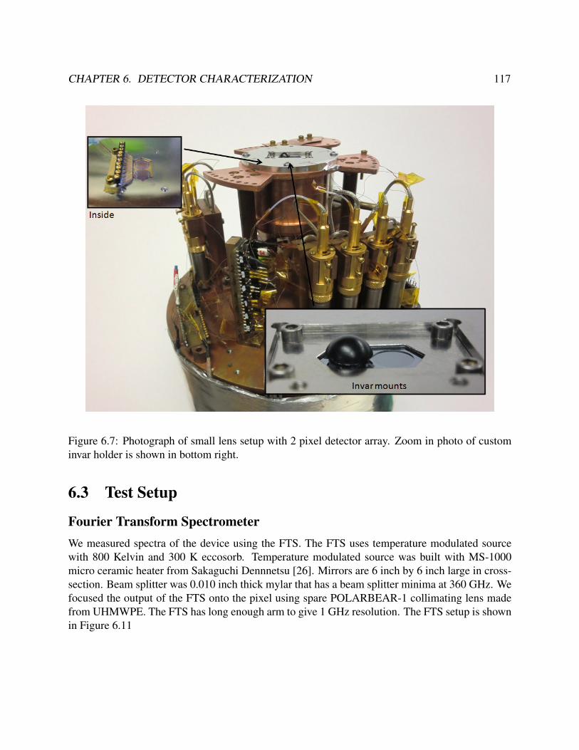
CHAPTER 6. DETECTOR CHARACTERIZATION 117
Figure 6.7: Photograph of small lens setup with 2 pixel detector array. Zoom in photo of custominvar holder is shown in bottom right.
6.3 Test Setup
Fourier Transform SpectrometerWe measured spectra of the device using the FTS. The FTS uses temperature modulated sourcewith 800 Kelvin and 300 K eccosorb. Temperature modulated source was built with MS-1000micro ceramic heater from Sakaguchi Dennnetsu [26]. Mirrors are 6 inch by 6 inch large in cross-section. Beam splitter was 0.010 inch thick mylar that has a beam splitter minima at 360 GHz. Wefocused the output of the FTS onto the pixel using spare POLARBEAR-1 collimating lens madefrom UHMWPE. The FTS has long enough arm to give 1 GHz resolution. The FTS setup is shownin Figure 6.11
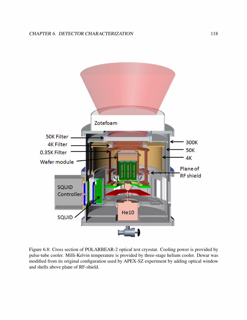
CHAPTER 6. DETECTOR CHARACTERIZATION 118
Figure 6.8: Cross section of POLARBEAR-2 optical test cryostat. Cooling power is provided bypulse-tube cooler. Milli-Kelvin temperature is provided by three-stage helium cooler. Dewar wasmodified from its original configuration used by APEX-SZ experiment by adding optical windowand shells above plane of RF-shield.
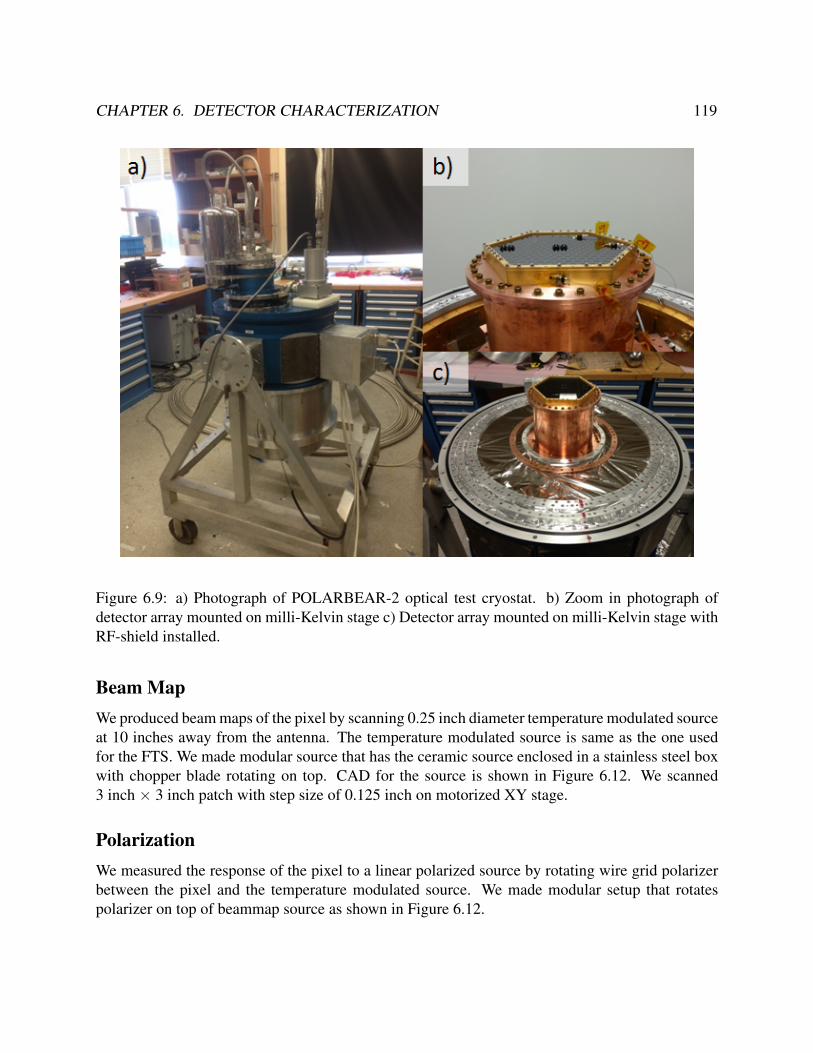
CHAPTER 6. DETECTOR CHARACTERIZATION 119
Figure 6.9: a) Photograph of POLARBEAR-2 optical test cryostat. b) Zoom in photograph ofdetector array mounted on milli-Kelvin stage c) Detector array mounted on milli-Kelvin stage withRF-shield installed.
Beam MapWe produced beam maps of the pixel by scanning 0.25 inch diameter temperature modulated sourceat 10 inches away from the antenna. The temperature modulated source is same as the one usedfor the FTS. We made modular source that has the ceramic source enclosed in a stainless steel boxwith chopper blade rotating on top. CAD for the source is shown in Figure 6.12. We scanned3 inch × 3 inch patch with step size of 0.125 inch on motorized XY stage.
PolarizationWe measured the response of the pixel to a linear polarized source by rotating wire grid polarizerbetween the pixel and the temperature modulated source. We made modular setup that rotatespolarizer on top of beammap source as shown in Figure 6.12.

CHAPTER 6. DETECTOR CHARACTERIZATION 120
Figure 6.10: Circuit diagram of dfMUX readout system [31]
Figure 6.11: Photograph of the FTS setup. Output of FTS is reflected upwards by 45 degree mirror.Then beam was focused into dewar. When making band measurement of detector, sample holdershown on bottom right is removed.
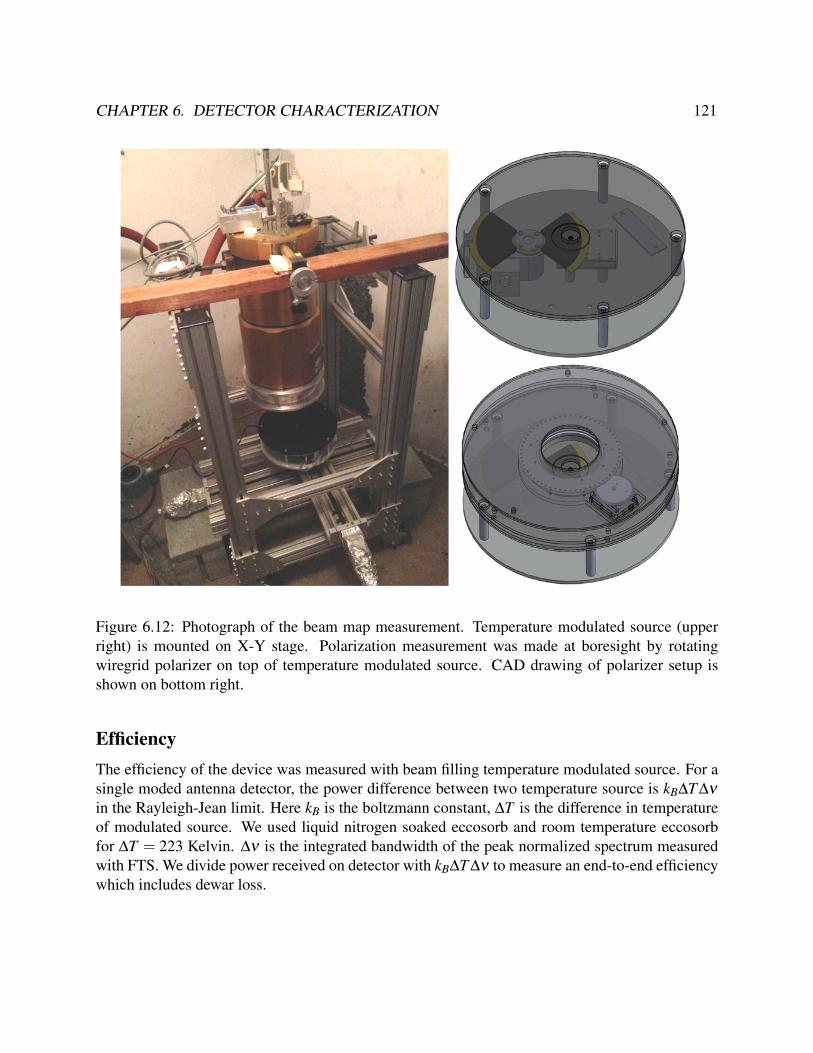
CHAPTER 6. DETECTOR CHARACTERIZATION 121
Figure 6.12: Photograph of the beam map measurement. Temperature modulated source (upperright) is mounted on X-Y stage. Polarization measurement was made at boresight by rotatingwiregrid polarizer on top of temperature modulated source. CAD drawing of polarizer setup isshown on bottom right.
EfficiencyThe efficiency of the device was measured with beam filling temperature modulated source. For asingle moded antenna detector, the power difference between two temperature source is kB∆T ∆ν
in the Rayleigh-Jean limit. Here kB is the boltzmann constant, ∆T is the difference in temperatureof modulated source. We used liquid nitrogen soaked eccosorb and room temperature eccosorbfor ∆T = 223 Kelvin. ∆ν is the integrated bandwidth of the peak normalized spectrum measuredwith FTS. We divide power received on detector with kB∆T ∆ν to measure an end-to-end efficiencywhich includes dewar loss.

CHAPTER 6. DETECTOR CHARACTERIZATION 122
Filter Type Number of Cell Type of lenslette Lumped InductorLumped Diplexer 16 6.35 mm PB-1 spare array MicrostripLumped Diplexer 16 14 mm MicrostripLumped Diplexer 11 14 mm CPWStub Diplexer 11 14 mm N/AStub Triplexer 11 14 mm N/A
Table 6.1: Summary of tested detectors
6.4 ResultMeasurements presented here were made with the 8 inch IR-Lab Dewar. The POLARBEAR-2optical cryostat is just coming online for testing, and it needs several calibration before we canmake quantitive statement. We will present initial measurements from the dewar to demonstrateits capability of testing large detector module qualitatively. We present results from distributeddiplexer with 11-cell sinuous antenna, distributed triplexer with 11-cell sinuous antenna, lumpedfilter diplexer with 11-cell sinuous antenna and lumped filter diplexer with 16-cell sinuous antennawith 14 mm silicon lenslette. We also present result from detector array with lumped diplexer and16-cell sinuous coupled with the POLARBEAR-1 spare 6.35 mm silicon lenslette array. One ofpolarization for 16-cell sinuous detector had open at crossover due to fabrication error, thus we willpresent measurement from one polarization. The detector with lumped filter with 11-cell sinuousantenna had lumped inductor fabricated from CPW. The detector with lumped filter with 16-cellsinuous antenna had lumped filter fabricated from microstripline. Types of detectors tested weresummarized in Table 6.1. The results from lab measurements are summarized in Table 6.2.
SpectrumThe interferogram from the FTS was apodized with triangular window function prior to the Fouriertransformation. Then the spectrum was divided by analytical beam splitter function to remove thebeam splitter effect [128]. The resulting spectra from distributed diplexer and distributed triplexerwith 11-cell sinuous antenna are shown in Figure 6.13. The spectra from lumped filter diplexerfrom 11-cell sinuous antenna and 16-cell sinuous antenna are shown in Figure 6.14. Peaks of thespectra were normalized to a measured optical efficiency of each band. The results show that wesuccessfully partitioned a broadband signal into 2 and 3 bands with matching band shape for or-thogonal polarizations. Figure 6.15 shows measurement from 16-cell sinuous antenna with lumpeddiplexer under POLARBEAR-1 lenslette array. This shows pixels that are close to each other havematching spectra. This measurement also shows that lumped filter with microstrip line as inductorleaks higher harmonics as expected from simulation. If we calculate loss-tangent using first har-monics and third harmonics peaks from 95GHz band after scaling them by expected efficienciesfrom simulation, we obtain loss-tangent of 6×10⁻³. However this loss-tangent would be too highfor expected efficiency calculated in Figugre 5.33. Measured optical efficiency includes filter loss

CHAPTER 6. DETECTOR CHARACTERIZATION 123
80 100 120 140 160 180 200 220
0
0.1
0.2
0.3
0.4
0.5
Frequency [GHz]
Effic
iency
95 GHz PolA95 GHz PolB
150 GHz PolA150 GHz PolB
80 100 120 140 160 180 200 220 240 2600
0.05
0.1
0.15
0.2
0.25
0.3
0.35
0.4
Frequency [GHz]
Effic
iency
95 GHz PolA95 GHz PolB150 GHz PolA150 GHz PolB220 GHz PolA220 GHz PolB
Figure 6.13: Spectrum of a distributed diplexer (left) and a distributed triplexer (right). A and Brefers to two orthogonal linear polarization channels. Peaks are normalized to the measured opticalefficiency. See Table 6.2 for details.
80 100 120 140 160 180 200
0
0.1
0.2
0.3
0.4
0.5
0.6
Frequency [GHz]
Effic
iency
95 GHz PolA95 GHz PolB
150 GHz PolA150 GHz PolB
50 100 150 2000
0.1
0.2
0.3
0.4
0.5
0.6
Frequency [GHz]
Eff
icie
ncy
90GHz
150GHz
Figure 6.14: Spectrum of a lumped diplexer with 11-cell sinuous antenna (left) and spectrum of alumped diplexer with 16-cell (right). A and B refers to two orthogonal linear polarization channels.Peaks are normalized to measured optical efficiency. See Table 6.2 for details.
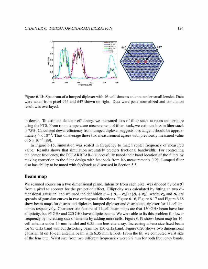
CHAPTER 6. DETECTOR CHARACTERIZATION 124
Figure 6.15: Spectrum of a lumped diplexer with 16-cell sinuous antenna under small lenslet. Datawere taken from pixel #45 and #47 shown on right. Data were peak normalized and simulationresult was overlayed.
in dewar. To estimate detector efficiency, we measured loss of filter stack at room temperatureusing the FTS. From room temperature measurement of filter stack, we estimate loss in filter stackis 75%. Calculated dewar efficiency from lumped diplexer suggests loss tangent should be approx-imately 4×10⁻³. Thus on average these two measurement agrees with previously measured valueof 5×10⁻³ [89].
In Figure 6.15, simulation was scaled in frequency to match center frequency of measuredvalue. Results shows that simulation accurately predicts fractional bandwidth. For controllingthe center frequency, the POLARBEAR-1 successfully tuned their band location of the filters bymaking correction to the filter design with feedback from lab measurements [12]. Lumped filteralso has ability to be tuned with feedback as discussed in Section 5.5.
Beam mapWe scanned source on a two dimensional plane. Intensity from each pixel was divided by cos(θ)from a pixel to account for the projection effect. Ellipticity was calculated by fitting an two di-mensional gaussian, and we used the definition ε = (|σa−σb|)/(σa +σb), where σa and σb arespreads of gaussian curves in two orthogonal directions. Figure 6.16, Figure 6.17 and Figure 6.18show beam maps for distributed diplexer, lumped diplexer and distributed triplexer for 11-cell an-tennas respectively. Characteristic feature of 11-cell beam maps are that 150 GHz beam have lowellipticity, but 95 GHz and 220 GHz have elliptic beams. We were able to fix this problem for lowerfrequency by increasing size of antenna by adding more cells. Figure 6.19 shows beam map for 16-cell antenna under 14 mm lenslet and 6.35 mm lenslette array. Increasing antena size fixed beamfor 95 GHz band without distorting beam for 150 GHz band. Figure 6.20 shows two dimensionalgaussian fit on 16-cell antenna beam with 6.35 mm lenslet. From the fit, we computed waist sizeof the lenslette. Waist size from two different frequencies were 2.2 mm for both frequency bands.

CHAPTER 6. DETECTOR CHARACTERIZATION 125
Figure 6.16: Beammap result from distributed diplexer. 95 GHz beam is shown on left and150 GHz beam is shown on right. See Figure 6.13 for exact band location. See Table 6.2 fordetails.
Since the lenslette was the POLARBEAR-1 spare lenslette, it placed antenna at L/R = 0.42. Bothlens-size and anti-reflection coating thicknesses are different between the POLARBEAR-1 and thePOLARBEAR-2, so direct comparison to the simulation is difficult. Suppose we compare mea-sured waist value to the simulated value since pixel-to-pixel spacing is same for both experiments,waist size agrees with the simulation.
PolarizationPolarization measurement results are shown in Figure 6.21 and tabulated at Table 6.2. We seea correlation between high ellipticity and high polarization leakage. Increasing antenna size for95 GHz channel also decreased polarization leakage. We expect the wiregrid to have approximately1% leakage, thus we are limited by systematics for low cross-pol measurement.
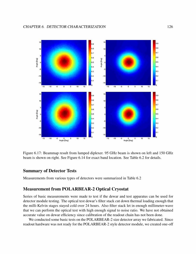
CHAPTER 6. DETECTOR CHARACTERIZATION 126
Figure 6.17: Beammap result from lumped diplexer. 95 GHz beam is shown on left and 150 GHzbeam is shown on right. See Figure 6.14 for exact band location. See Table 6.2 for details.
Summary of Detector TestsMeasurements from various types of detectors were summarized in Table 6.2
Measurement from POLARBEAR-2 Optical CryostatSeries of basic measurements were made to test if the dewar and test apparatus can be used fordetector module testing. The optical test dewar’s filter stack cut down thermal loading enough thatthe milli-Kelvin stages stayed cold over 24 hours. Also filter stack let in enough millimeter-wavethat we can perform the optical test with high enough signal to noise ratio. We have not obtainedaccurate value on dewar efficiency since calibration of the readout chain has not been done.
We conducted some basic tests on the POLARBEAR-2 size detector array we fabricated. Sincereadout hardware was not ready for the POLARBEAR-2 style detector module, we created one-off
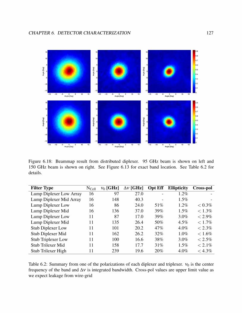
CHAPTER 6. DETECTOR CHARACTERIZATION 127
Figure 6.18: Beammap result from distributed diplexer. 95 GHz beam is shown on left and150 GHz beam is shown on right. See Figure 6.13 for exact band location. See Table 6.2 fordetails.
Filter Type NCell ν0 [GHz] ∆ν [GHz] Opt Eff Ellipticity Cross-polLump Diplexer Low Array 16 97 27.0 - 1.2% -Lump Diplexer Mid Array 16 148 40.3 - 1.5% -Lump Diplexer Low 16 86 24.0 51% 1.2% < 0.3%Lump Diplexer Mid 16 136 37.0 39% 1.5% < 1.3%Lump Diplexer Low 11 87 17.0 39% 3.0% < 2.9%Lump Diplexer Mid 11 135 26.4 50% 4.5% < 1.7%Stub Diplexer Low 11 101 20.2 47% 4.0% < 2.3%Stub Diplexer Mid 11 162 26.2 32% 1.0% < 1.6%Stub Triplexer Low 11 100 16.6 38% 3.0% < 2.5%Stub Trilexer Mid 11 158 17.7 31% 1.5% < 2.1%Stub Trilexer High 11 239 19.6 20% 4.0% < 4.3%
Table 6.2: Summary from one of the polarizations of each diplexer and triplexer. ν0 is the centerfrequency of the band and ∆ν is integrated bandwidth. Cross-pol values are upper limit value aswe expect leakage from wire-grid
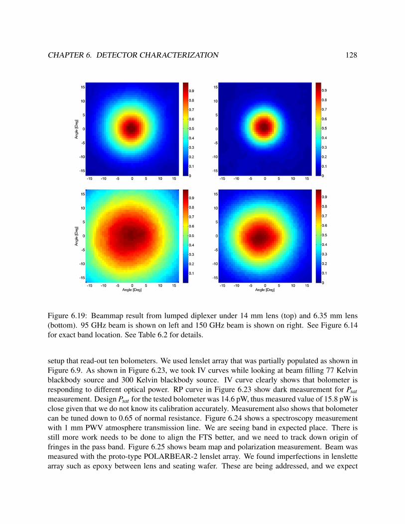
CHAPTER 6. DETECTOR CHARACTERIZATION 128
Figure 6.19: Beammap result from lumped diplexer under 14 mm lens (top) and 6.35 mm lens(bottom). 95 GHz beam is shown on left and 150 GHz beam is shown on right. See Figure 6.14for exact band location. See Table 6.2 for details.
setup that read-out ten bolometers. We used lenslet array that was partially populated as shown inFigure 6.9. As shown in Figure 6.23, we took IV curves while looking at beam filling 77 Kelvinblackbody source and 300 Kelvin blackbody source. IV curve clearly shows that bolometer isresponding to different optical power. RP curve in Figure 6.23 show dark measurement for Psatmeasurement. Design Psat for the tested bolometer was 14.6 pW, thus measured value of 15.8 pW isclose given that we do not know its calibration accurately. Measurement also shows that bolometercan be tuned down to 0.65 of normal resistance. Figure 6.24 shows a spectroscopy measurementwith 1 mm PWV atmosphere transmission line. We are seeing band in expected place. There isstill more work needs to be done to align the FTS better, and we need to track down origin offringes in the pass band. Figure 6.25 shows beam map and polarization measurement. Beam wasmeasured with the proto-type POLARBEAR-2 lenslet array. We found imperfections in lenslettearray such as epoxy between lens and seating wafer. These are being addressed, and we expect
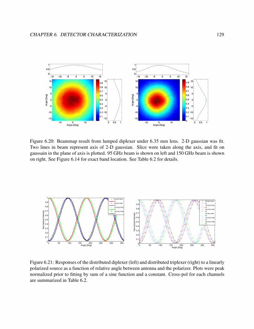
CHAPTER 6. DETECTOR CHARACTERIZATION 129
Figure 6.20: Beammap result from lumped diplexer under 6.35 mm lens. 2-D gaussian was fit.Two lines in beam represent axis of 2-D gaussian. Slice were taken along the axis, and fit ongaussain in the plane of axis is plotted. 95 GHz beam is shown on left and 150 GHz beam is shownon right. See Figure 6.14 for exact band location. See Table 6.2 for details.
0 50 100 150 200 250 300 3500
0.1
0.2
0.3
0.4
0.5
0.6
0.7
0.8
0.9
1
Angle [Deg]
Norm
aliz
ed Inte
nsity
95 GHz PolA
Fit
95 GHz PolB
Fit
150 GHz PolA
Fit
150 GHz PolB
Fit
0 50 100 150 200 250 300 3500
0.1
0.2
0.3
0.4
0.5
0.6
0.7
0.8
0.9
1
Angle [Deg]
No
rma
lize
d I
nte
nsity
95 GHz PolA
Fit
150 GHz PolA
Fit
220 GHz PolA
Fit
95 GHz PolB
Fit
150 GHz PolB
Fit
220 GHz PolB
Fit
Figure 6.21: Responses of the distributed diplexer (left) and distributed triplexer (right) to a linearlypolarized source as a function of relative angle between antenna and the polarizer. Plots were peaknormalized prior to fitting by sum of a sine function and a constant. Cross-pol for each channelsare summarized in Table 6.2.

CHAPTER 6. DETECTOR CHARACTERIZATION 130
0 20 40 60 80 100 120 140 160 1800
0.1
0.2
0.3
0.4
0.5
0.6
0.7
0.8
0.9
1
Angle [Deg]
No
rma
lize
d I
nte
nsity
95 GHz PolA
Fit
150 GHz PolA
Fit
95 GHz PolB
Fit
150 GHz PolA
Fit
0 50 100 150 200 250 300 3500
0.1
0.2
0.3
0.4
0.5
0.6
0.7
0.8
0.9
1
Angle [Deg]
Norm
aliz
ed Inte
nsity
95 GHz PolA
Fit
150 GHz PolA
Fit
Figure 6.22: Responses of the lumped diplexer with 11-cell sinuous antenna (left) and lumpeddiplexer with 16-cell sinuous antenna (right) to a linearly polarized source as a function of relativeangle between antenna and the polarizer. Plots were peak normalized prior to fitting by sum of asine function and a constant. Cross-pol for each channels are summarized in Table 6.2.
Figure 6.23: (left) I-V curve while detector is receiving optical locating from 300 Kelvin load and77 Kelvin load. (right) I-V curve and R-P curve showing that detector biased down to 0.65RN .
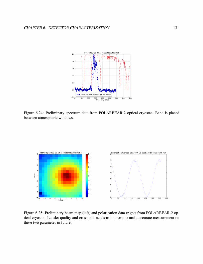
CHAPTER 6. DETECTOR CHARACTERIZATION 131
Figure 6.24: Preliminary spectrum data from POLARBEAR-2 optical cryostat. Band is placedbetween atmospheric windows.
Figure 6.25: Preliminary beam map (left) and polarization data (right) from POLARBEAR-2 op-tical cryostat. Lenslet quality and cross-talk needs to improve to make accurate measurement onthese two parametes in future.

CHAPTER 6. DETECTOR CHARACTERIZATION 132
similar or better beam performance that we obtained with POLARBEAR-1 spare lenslette array.Polarization measurement shows expected sinusoidal responce. Its cross-polarization leakage suf-fered from cross-talk from neighboring channel since measurement was done with aluminum TESwhich has higher resistance value. We can operate bolometer at lower resistance AlTi transitionwith cryogenically cooled attenuating filter. Lower RT ES would reduce the cross-talk effect. Col-laborating institutions are building test dewar based on the design of this dewar such that we cancompare results in similar condition.
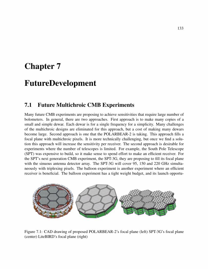
133
Chapter 7
FutureDevelopment
7.1 Future Multichroic CMB ExperimentsMany future CMB experiments are proposing to achieve sensitivities that require large number ofbolometers. In general, there are two approaches. First approach is to make many copies of asmall and simple dewar. Each dewar is for a single frequency for a simplicity. Many challengesof the multichroic designs are eliminated for this approach, but a cost of making many dewarsbecome large. Second approach is one that the POLARBEAR-2 is taking. This approach fills afocal plane with multichroic pixels. It is more technically challenging, but once we find a solu-tion this approach will increase the sensitivity per receiver. The second approach is desirable forexperiments where the number of telescopes is limited. For example, the South Pole Telescope(SPT) was expensive to build, so it make sense to spend effort to make an efficient receiver. Forthe SPT’s next generation CMB experiment, the SPT-3G, they are proposing to fill its focal planewith the sinuous antenna detector array. The SPT-3G will cover 95, 150 and 220 GHz simulta-neously with triplexing pixels. The balloon experiment is another experiment where an efficientreceiver is beneficial. The balloon experiment has a tight weight budget, and its launch opportu-
Figure 7.1: CAD drawing of proposed POLARBEAR-2’s focal plane (left) SPT-3G’s focal plane(center) LiteBIRD’s focal plane (right)
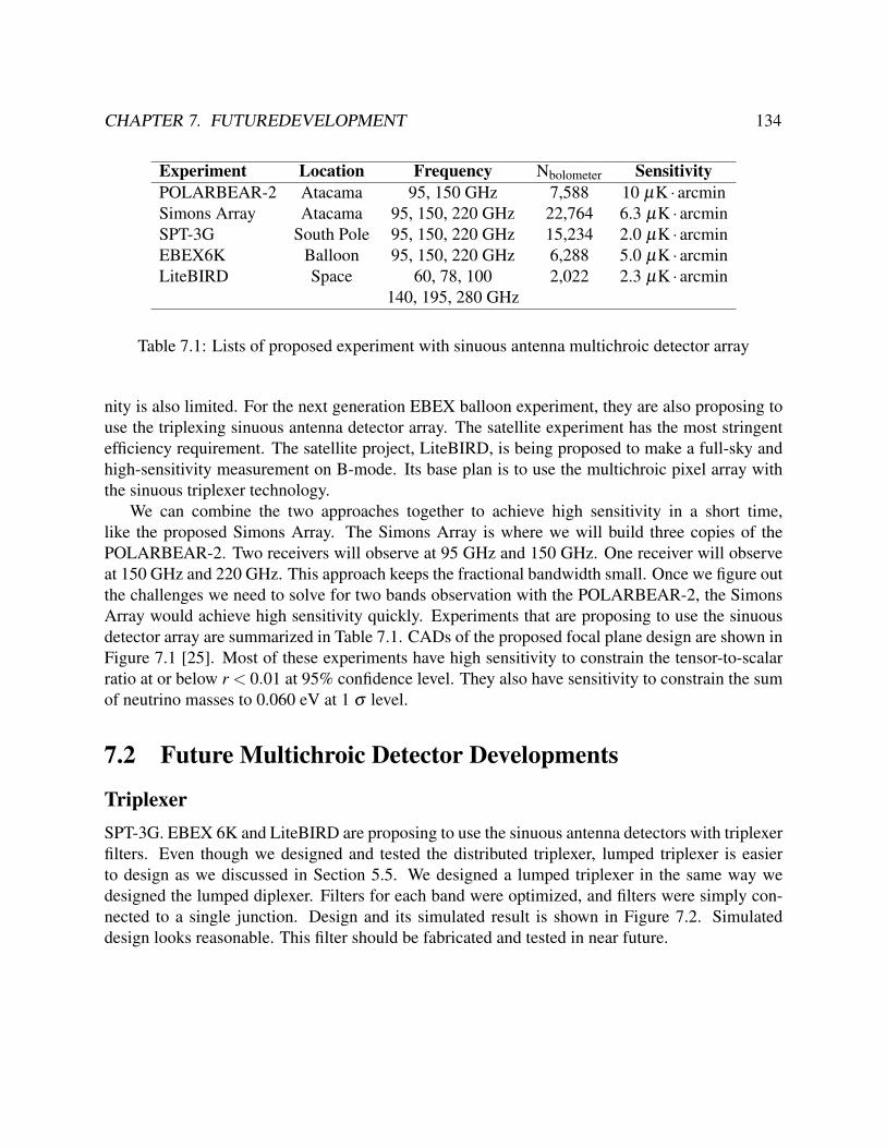
CHAPTER 7. FUTUREDEVELOPMENT 134
Experiment Location Frequency Nbolometer SensitivityPOLARBEAR-2 Atacama 95, 150 GHz 7,588 10 µK · arcminSimons Array Atacama 95, 150, 220 GHz 22,764 6.3 µK · arcminSPT-3G South Pole 95, 150, 220 GHz 15,234 2.0 µK · arcminEBEX6K Balloon 95, 150, 220 GHz 6,288 5.0 µK · arcminLiteBIRD Space 60, 78, 100 2,022 2.3 µK · arcmin
140, 195, 280 GHz
Table 7.1: Lists of proposed experiment with sinuous antenna multichroic detector array
nity is also limited. For the next generation EBEX balloon experiment, they are also proposing touse the triplexing sinuous antenna detector array. The satellite experiment has the most stringentefficiency requirement. The satellite project, LiteBIRD, is being proposed to make a full-sky andhigh-sensitivity measurement on B-mode. Its base plan is to use the multichroic pixel array withthe sinuous triplexer technology.
We can combine the two approaches together to achieve high sensitivity in a short time,like the proposed Simons Array. The Simons Array is where we will build three copies of thePOLARBEAR-2. Two receivers will observe at 95 GHz and 150 GHz. One receiver will observeat 150 GHz and 220 GHz. This approach keeps the fractional bandwidth small. Once we figure outthe challenges we need to solve for two bands observation with the POLARBEAR-2, the SimonsArray would achieve high sensitivity quickly. Experiments that are proposing to use the sinuousdetector array are summarized in Table 7.1. CADs of the proposed focal plane design are shown inFigure 7.1 [25]. Most of these experiments have high sensitivity to constrain the tensor-to-scalarratio at or below r < 0.01 at 95% confidence level. They also have sensitivity to constrain the sumof neutrino masses to 0.060 eV at 1 σ level.
7.2 Future Multichroic Detector Developments
TriplexerSPT-3G. EBEX 6K and LiteBIRD are proposing to use the sinuous antenna detectors with triplexerfilters. Even though we designed and tested the distributed triplexer, lumped triplexer is easierto design as we discussed in Section 5.5. We designed a lumped triplexer in the same way wedesigned the lumped diplexer. Filters for each band were optimized, and filters were simply con-nected to a single junction. Design and its simulated result is shown in Figure 7.2. Simulateddesign looks reasonable. This filter should be fabricated and tested in near future.
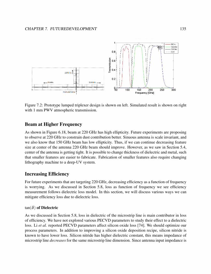
CHAPTER 7. FUTUREDEVELOPMENT 135
Figure 7.2: Prototype lumped triplexer design is shown on left. Simulated result is shown on rightwith 1 mm PWV atmospheric transmission.
Beam at Higher FrequencyAs shown in Figure 6.18, beam at 220 GHz has high ellipticity. Future experiments are proposingto observe at 220 GHz to constrain dust contribution better. Sinuous antenna is scale invariant, andwe also know that 150 GHz beam has low ellipticity. Thus, if we can continue decreasing featuresize at center of the antenna 220 GHz beam should improve. However, as we saw in Section 5.4,center of the antenna is getting tight. It is possible to change thickness of dielectric and metal, suchthat smaller features are easier to fabricate. Fabrication of smaller features also require changinglithography machine to a deep-UV system.
Increasing EfficiencyFor future experiments that are targeting 220 GHz, decreasing efficiency as a function of frequencyis worrying. As we discussed in Section 5.8, loss as function of frequency we see efficiencymeasurement follows dielectric loss model. In this section, we will discuss various ways we canmitigate efficiency loss due to dielectric loss.
tan(δ ) of Dielectric
As we discussed in Section 5.8, loss in dielectric of the microstrip line is main contributor in lossof efficiency. We have not explored various PECVD parameters to study their effect to a dielectricloss. Li et al. reported PECVD parameters affect silicon oxide loss [74]. We should optimize ourprocess parameters. In addition to improving a silicon oxide deposition recipe, silicon nitride isknown to have lower loss. Silicon nitride has higher dielectric constant, this means impedance ofmicrostrip line decreases for the same microstrip line dimension. Since antenna input impedance is
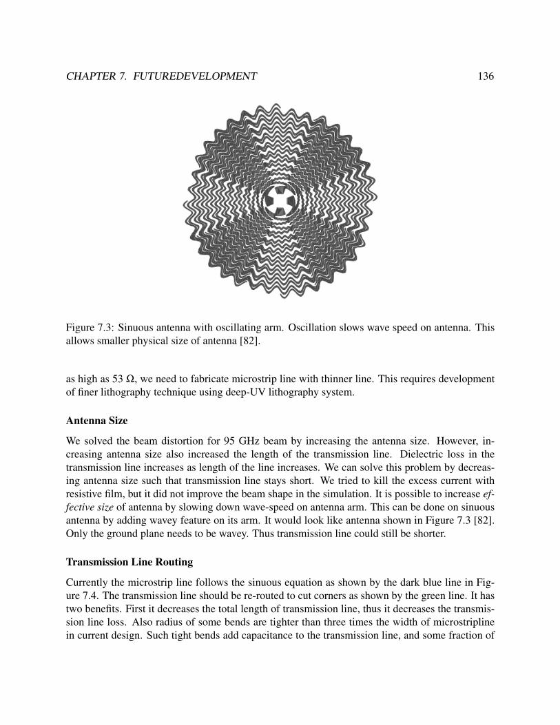
CHAPTER 7. FUTUREDEVELOPMENT 136
Figure 7.3: Sinuous antenna with oscillating arm. Oscillation slows wave speed on antenna. Thisallows smaller physical size of antenna [82].
as high as 53 Ω, we need to fabricate microstrip line with thinner line. This requires developmentof finer lithography technique using deep-UV lithography system.
Antenna Size
We solved the beam distortion for 95 GHz beam by increasing the antenna size. However, in-creasing antenna size also increased the length of the transmission line. Dielectric loss in thetransmission line increases as length of the line increases. We can solve this problem by decreas-ing antenna size such that transmission line stays short. We tried to kill the excess current withresistive film, but it did not improve the beam shape in the simulation. It is possible to increase ef-fective size of antenna by slowing down wave-speed on antenna arm. This can be done on sinuousantenna by adding wavey feature on its arm. It would look like antenna shown in Figure 7.3 [82].Only the ground plane needs to be wavey. Thus transmission line could still be shorter.
Transmission Line Routing
Currently the microstrip line follows the sinuous equation as shown by the dark blue line in Fig-ure 7.4. The transmission line should be re-routed to cut corners as shown by the green line. It hastwo benefits. First it decreases the total length of transmission line, thus it decreases the transmis-sion line loss. Also radius of some bends are tighter than three times the width of microstriplinein current design. Such tight bends add capacitance to the transmission line, and some fraction of
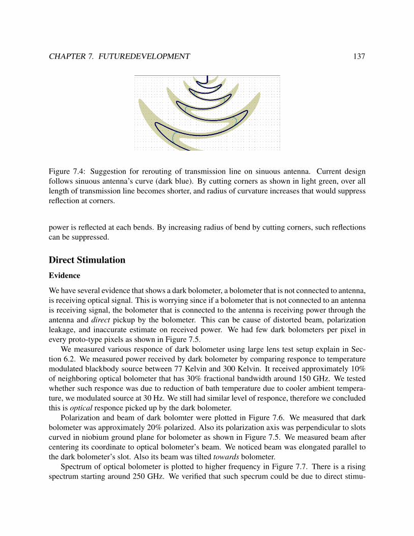
CHAPTER 7. FUTUREDEVELOPMENT 137
Figure 7.4: Suggestion for rerouting of transmission line on sinuous antenna. Current designfollows sinuous antenna’s curve (dark blue). By cutting corners as shown in light green, over alllength of transmission line becomes shorter, and radius of curvature increases that would suppressreflection at corners.
power is reflected at each bends. By increasing radius of bend by cutting corners, such reflectionscan be suppressed.
Direct StimulationEvidence
We have several evidence that shows a dark bolometer, a bolometer that is not connected to antenna,is receiving optical signal. This is worrying since if a bolometer that is not connected to an antennais receiving signal, the bolometer that is connected to the antenna is receiving power through theantenna and direct pickup by the bolometer. This can be cause of distorted beam, polarizationleakage, and inaccurate estimate on received power. We had few dark bolometers per pixel inevery proto-type pixels as shown in Figure 7.5.
We measured various responce of dark bolometer using large lens test setup explain in Sec-tion 6.2. We measured power received by dark bolometer by comparing responce to temperaturemodulated blackbody source between 77 Kelvin and 300 Kelvin. It received approximately 10%of neighboring optical bolometer that has 30% fractional bandwidth around 150 GHz. We testedwhether such responce was due to reduction of bath temperature due to cooler ambient tempera-ture, we modulated source at 30 Hz. We still had similar level of responce, therefore we concludedthis is optical responce picked up by the dark bolometer.
Polarization and beam of dark bolomter were plotted in Figure 7.6. We measured that darkbolometer was approximately 20% polarized. Also its polarization axis was perpendicular to slotscurved in niobium ground plane for bolometer as shown in Figure 7.5. We measured beam aftercentering its coordinate to optical bolometer’s beam. We noticed beam was elongated parallel tothe dark bolometer’s slot. Also its beam was tilted towards bolometer.
Spectrum of optical bolometer is plotted to higher frequency in Figure 7.7. There is a risingspectrum starting around 250 GHz. We verified that such specrum could be due to direct stimu-
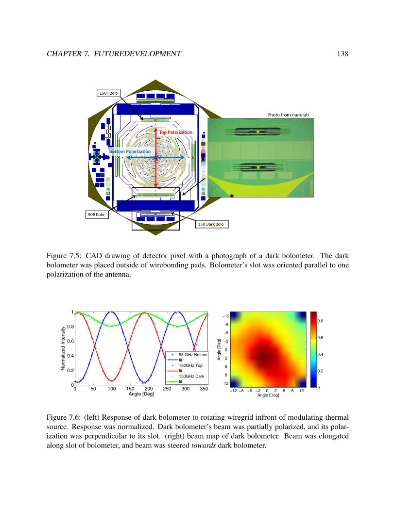
CHAPTER 7. FUTUREDEVELOPMENT 138
Figure 7.5: CAD drawing of detector pixel with a photograph of a dark bolometer. The darkbolometer was placed outside of wirebonding pads. Bolometer’s slot was oriented parallel to onepolarization of the antenna.
0 50 100 150 200 250 300 3500
0.2
0.4
0.6
0.8
1
Angle [Deg]
No
rma
lize
d I
nte
nsity
95 GHz Bottom
fit
150GHz Top
fit
150GHz Dark
fit
Angle [Deg]
An
gle
[D
eg
]
−12 −8 −6 −2 0 2 6 8 12
−12
−8
−6
−2
0
2
6
8
12 0
0.2
0.4
0.6
0.8
Figure 7.6: (left) Response of dark bolometer to rotating wiregrid infront of modulating thermalsource. Response was normalized. Dark bolometer’s beam was partially polarized, and its polar-ization was perpendicular to its slot. (right) beam map of dark bolometer. Beam was elongatedalong slot of bolometer, and beam was steered towards dark bolometer.
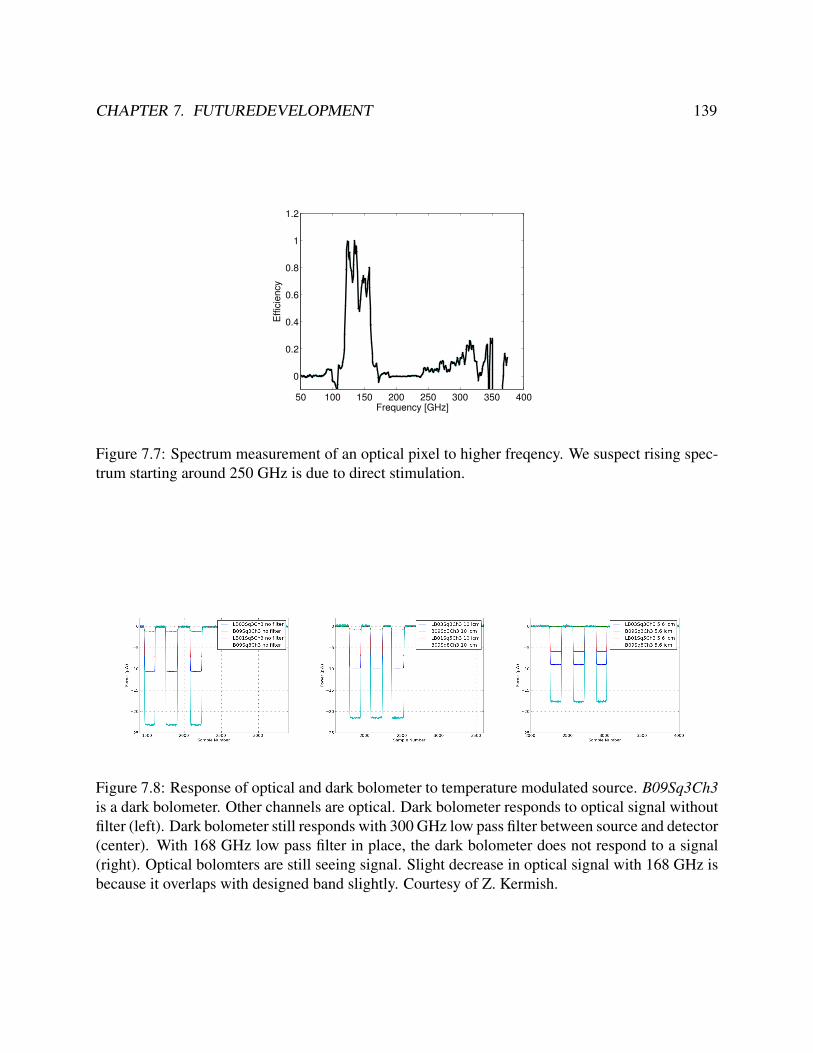
CHAPTER 7. FUTUREDEVELOPMENT 139
50 100 150 200 250 300 350 400
0
0.2
0.4
0.6
0.8
1
1.2
Frequency [GHz]
Effic
iency
Figure 7.7: Spectrum measurement of an optical pixel to higher freqency. We suspect rising spec-trum starting around 250 GHz is due to direct stimulation.
Figure 7.8: Response of optical and dark bolometer to temperature modulated source. B09Sq3Ch3is a dark bolometer. Other channels are optical. Dark bolometer responds to optical signal withoutfilter (left). Dark bolometer still responds with 300 GHz low pass filter between source and detector(center). With 168 GHz low pass filter in place, the dark bolometer does not respond to a signal(right). Optical bolomters are still seeing signal. Slight decrease in optical signal with 168 GHz isbecause it overlaps with designed band slightly. Courtesy of Z. Kermish.
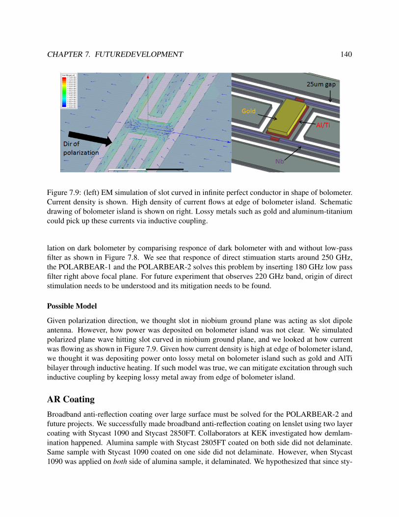
CHAPTER 7. FUTUREDEVELOPMENT 140
Figure 7.9: (left) EM simulation of slot curved in infinite perfect conductor in shape of bolometer.Current density is shown. High density of current flows at edge of bolometer island. Schematicdrawing of bolometer island is shown on right. Lossy metals such as gold and aluminum-titaniumcould pick up these currents via inductive coupling.
lation on dark bolometer by comparising responce of dark bolometer with and without low-passfilter as shown in Figure 7.8. We see that responce of direct stimuation starts around 250 GHz,the POLARBEAR-1 and the POLARBEAR-2 solves this problem by inserting 180 GHz low passfilter right above focal plane. For future experiment that observes 220 GHz band, origin of directstimulation needs to be understood and its mitigation needs to be found.
Possible Model
Given polarization direction, we thought slot in niobium ground plane was acting as slot dipoleantenna. However, how power was deposited on bolometer island was not clear. We simulatedpolarized plane wave hitting slot curved in niobium ground plane, and we looked at how currentwas flowing as shown in Figure 7.9. Given how current density is high at edge of bolometer island,we thought it was depositing power onto lossy metal on bolometer island such as gold and AlTibilayer through inductive heating. If such model was true, we can mitigate excitation through suchinductive coupling by keeping lossy metal away from edge of bolometer island.
AR CoatingBroadband anti-reflection coating over large surface must be solved for the POLARBEAR-2 andfuture projects. We successfully made broadband anti-reflection coating on lenslet using two layercoating with Stycast 1090 and Stycast 2850FT. Collaborators at KEK investigated how demlam-ination happened. Alumina sample with Stycast 2805FT coated on both side did not delaminate.Same sample with Stycast 1090 coated on one side did not delaminate. However, when Stycast1090 was applied on both side of alumina sample, it delaminated. We hypothesized that since sty-
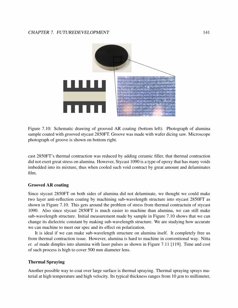
CHAPTER 7. FUTUREDEVELOPMENT 141
Figure 7.10: Schematic drawing of grooved AR coating (bottom left). Photograph of aluminasample coated with grooved stycast 2850FT. Groove was made with wafer dicing saw. Microscopephotograph of groove is shown on bottom right.
cast 2850FT’s thermal contraction was reduced by adding ceramic filler, that thermal contractiondid not exert great stress on alumina. However, Stycast 1090 is a type of epoxy that has many voidsimbedded into its mixture, thus when cooled such void contract by great amount and delaminatesfilm.
Grooved AR coating
Since stycast 2850FT on both sides of alumina did not delaminate, we thought we could maketwo layer anti-reflection coating by machining sub-wavelength structure into stycast 2850FT asshown in Figure 7.10. This gets around the problem of stress from thermal contractuin of stycast1090. Also since stycast 2850FT is much easier to machine than alumina, we can still makesub-wavelength structure. Initial measurement made by sample in Figure 7.10 shows that we canchange its dielectric constant by making sub-wavelength structure. We are studying how accuratewe can machine to meet our spec and its effect on polarization.
It is ideal if we can make sub-wavelength structure on alumina itself. It completely free usfrom thermal contraction issue. However, alumina is hard to machine in conventional way. Nittaet. al made dimples into alumina with laser pulses as shown in Figure 7.11 [119]. Time and costof such process is high to cover 500 mm diameter lens.
Thermal Spraying
Another possible way to coat over large surface is thermal spraying. Thermal spraying sprays ma-terial at high temperature and high velocity. Its typical thickness ranges from 10 µm to millimeter,
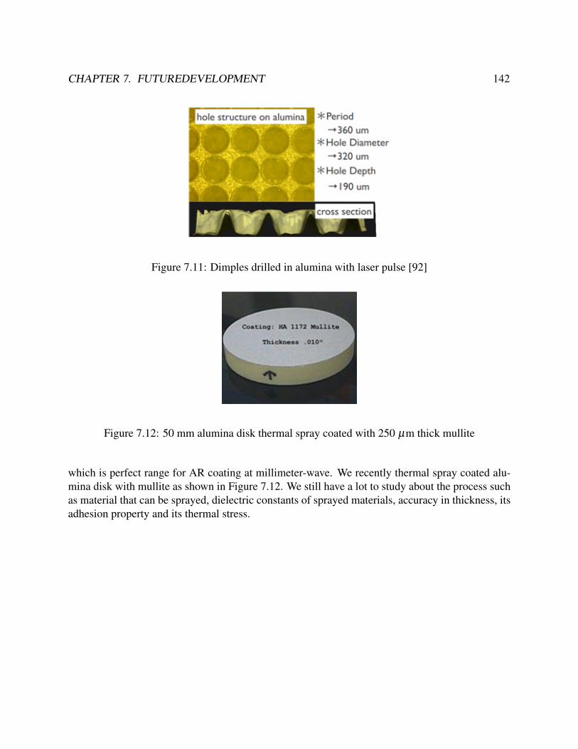
CHAPTER 7. FUTUREDEVELOPMENT 142
Figure 7.11: Dimples drilled in alumina with laser pulse [92]
Figure 7.12: 50 mm alumina disk thermal spray coated with 250 µm thick mullite
which is perfect range for AR coating at millimeter-wave. We recently thermal spray coated alu-mina disk with mullite as shown in Figure 7.12. We still have a lot to study about the process suchas material that can be sprayed, dielectric constants of sprayed materials, accuracy in thickness, itsadhesion property and its thermal stress.

143
Bibliography
[1] P.A.R. Ade et al. “Planck 2013 results. XVI. Cosmological parameters”. In: (2013). arXiv:1303.5076 [astro-ph.CO].
[2] P.A.R. Ade et al. “Planck 2013 results. XXII. Constraints on inflation”. In: (2013). arXiv:1303.5082 [astro-ph.CO].
[3] P.A.R. Ade et al. “Planck 2013 results. XXIII. Isotropy and Statistics of the CMB”. In:(2013). arXiv: 1303.5083 [astro-ph.CO].
[4] P.A.R. Ade et al. “Planck 2013 Results. XXIV. Constraints on primordial non-Gaussianity”.In: (2013). arXiv: 1303.5084 [astro-ph.CO].
[5] N. Aghanim et al. “Planck 2013 results. XXVII. Doppler boosting of the CMB: Eppur simuove”. In: (2013). arXiv: 1303.5087 [astro-ph.CO].
[6] Karim Mohammad Pour Aghdam, Reza Faraji-Dana, and Jalil Rashed-Mohassel. “Thesinuous antenna-A dual polarized feed for reflector-based searching systems”. In: AEU- International Journal of Electronics and Communications 59.7 (2005), pp. 392 –400.ISSN: 1434-8411. DOI: http://dx.doi.org/10.1016/j.aeue.2004.11.046. URL:http://www.sciencedirect.com/science/article/pii/S1434841104000639.
[7] Neil McN. Alford and Stuart J. Penn. “Sintered alumina with low dielectric loss”. In: Jour-nal of Applied Physics 80.10 (1996).
[8] ALMA. Atacama Large Millimeter/submillimeter Array. 2013. URL: http://www.apex-telescope.org/weather/.
[9] R. A. Alpher, H. Bethe, and G. Gamow. “The Origin of Chemical Elements”. In: Phys.Rev. 73 (7 1948), pp. 803–804. DOI: 10.1103/PhysRev.73.803. URL: http://link.aps.org/doi/10.1103/PhysRev.73.803.
[10] Inc. ANSYS. ANSYS HFSS. 2013. URL: http://www.ansys.com/.
[11] Evan H. Appleman. “Reaction of xenon difluoride with water and with xenon trioxide”. In:Inorg. Chem. 6.7 (1967), pp. 1305–1310.
[12] K. Arnold. “Design and Deployment of the POLARBEAR Cosmic Microwave BackgroundPolarization Experiment”. PhD thesis. University of California, Berkeley, 2010.
[13] K. Arnold et al. The bolometric focal plane array of the POLARBEAR CMB experiment.2012. DOI: 10.1117/12.927057. URL: http://dx.doi.org/10.1117/12.927057.
BIBLIOGRAPHY 144
[14] H.A. Leupold A.T. Hirshfeld and H.A. Boorse. “Superconducting and Normal SpecificHeat of Niobium”. In: Physical Review 127.5 (1962).
[15] F. Aubin. “Bolometer Noise Calculation Memo”. In: (2009).
[16] A. Babinet. “Memoires d’optique meteorologique”. In: Comp. Rend. Acad. Sci 4.638 (1837).
[17] C. Bischoff et al. “First Season QUIET Observations: Measurements of CMB Polariza-tion Power Spectra at 43 GHz in the Multipole Range 25 <= ell <= 475”. In: Astro-phys.J. 741 (2011), p. 111. DOI: 10.1088/0004-637X/741/2/111. arXiv: 1012.3191[astro-ph.CO].
[18] J. J. Bock. “Rocket-borne observation of singly ionized carbon 158 um emission from thediffuse interstellar medium”. PhD thesis. University of California, Berkeley, 1994.
[19] James Bock et al. “Task force on cosmic microwave background research”. In: (2006).arXiv: astro-ph/0604101 [astro-ph].
[20] H. Booker. “Slot Aerials and Their Relation to Complementary Wire Aerials”. In: J.I.E.E.93.620 (1946).
[21] M. Born and E. Wolf. Principles of Optics. 1999.
[22] W. S. BOYLE and JR. K. F. RODGERS. “Performance Characteristics of a New Low-Temperature Bolometer”. In: J. Opt. Soc. Am. 49.1 (1959), pp. 66–69. DOI: 10.1364/JOSA.49.000066. URL: http://www.opticsinfobase.org/abstract.cfm?URI=josa-49-1-66.
[23] M.C. Buck and D.S. Filipovic. “Split-beam mode four-arm slot sinuous antenna”. In: An-tennas and Wireless Propagation Letters, IEEE 3.1 (2004), pp. 83–86. ISSN: 1536-1225.DOI: 10.1109/LAWP.2004.830004.
[24] H.C. Chiang et al. “Measurement of CMB Polarization Power Spectra from Two Yearsof BICEP Data”. In: Astrophys.J. 711 (2010), pp. 1123–1140. DOI: 10 . 1088 / 0004 -637X/711/2/1123. arXiv: 0906.1181 [astro-ph.CO].
[25] CMB2013. International Conference on Cosmic Microwave Background, CMB2013, Oki-nawa, Japan. 2013. URL: http://www-conf.kek.jp/cmb/2013/.
[26] Sakaguchi E.H VOC Corp. Sakaguchi E.H VOC Corp. 2013. URL: http://www.sakaguchi.com/gbp/.
[27] D. P. Neikirk D. B. Rutledge and D. P. Kasilingam. Integrated circuit antennas, in Infraredand Millimeter-Waves. Ed. by K. J. Button. 1983.
[28] Brian Keating William Krantz Adrian T. Lee Erin Quealy Paul L. Richards Praween Siri-tanasak Darin Rosen Aritoki Suzuki and William Walker. “ Epoxy-based broadband anti-reflection coating for millimeter-wave optics,” in: Applied Optics (2013 Accepted).
[29] G. Deschamps. “Impedance Properties of Complementary Multiterminal Planar Struc-tures”. In: Antennas and Propagation, IEEE Transaction 7.5 (1959), pp. 371–378.
BIBLIOGRAPHY 145
[30] R. H. Dicke et al. “Cosmic Black-Body Radiation.” In: The Astrophysical Journal 142(1965), pp. 414–419. DOI: 10.1086/148306.
[31] M. A. Dobbs et al. “Frequency multiplexed superconducting quantum interference devicereadout of large bolometer arrays for cosmic microwave background measurements”. In:Review of Scientific Instruments 83.7, 073113 (2012), pp. –. DOI: http://dx.doi.org/10.1063/1.4737629. URL: http://scitation.aip.org/content/aip/journal/rsi/83/7/10.1063/1.4737629.
[32] R. Duhamel. Dual Polarized Sinuous Antennas. United States Patent 4658262. 1987.
[33] J.M. Edwards et al. “Dual-Polarized Sinuous Antennas on Extended Hemispherical SiliconLenses”. In: Antennas and Propagation, IEEE Transactions on 60.9 (2012), pp. 4082–4091. ISSN: 0018-926X. DOI: 10.1109/TAP.2012.2207048.
[34] ESA. Planck. 2013. URL: http://www.esa.int/Our_Activities/Space_Science/Planck.
[35] D.F. Filipovic, S.S. Gearhart, and G.M. Rebeiz. “Double-slot antennas on extended hemi-spherical and elliptical silicon dielectric lenses”. In: Microwave Theory and Techniques,IEEE Transactions on 41.10 (1993), pp. 1738–1749. ISSN: 0018-9480. DOI: 10.1109/22.247919.
[36] D.J. Fixsen. “The Temperature of the Cosmic Microwave Background”. In: Astrophys.J.707 (2009), pp. 916–920. DOI: 10.1088/0004-637X/707/2/916. arXiv: 0911.1955[astro-ph.CO].
[37] J.W. Fowler. “The Atacama Cosmology Telescope project”. In: Proceedings of SPIE (2004),p. 5498.
[38] E.M.T. Jones G. Matthaei and L. Young. Microwave Filters, Impedance-Matching Net-works, and Coupling Structures. Artech House, 1980.
[39] G Gamow. “Expanding Universe and the Origin of Elements”. In: The Physical Review 70(1946), p. 572.
[40] J.M. Gildemeister. “Voltage-Biased Superconducting Bolometers for Infrared and mm-Waves”. PhD thesis. University of California, Berkeley, 1995.
[41] Matthew J. Griffin, James J. Bock, and Walter K. Gear. “Relative Performance of Filledand Feedhorn-Coupled Focal-Plane Architectures”. In: Appl. Opt. 41.31 (2002), pp. 6543–6554. DOI: 10.1364/AO.41.006543. URL: http://ao.osa.org/abstract.cfm?URI=ao-41-31-6543.
[42] Tijmen de Haan et al. “Improved performance of TES bolometers using digital feedback”.In: (2012), 84520E–84520E–10. DOI: 10.1117/12.925658. URL: +http://dx.doi.org/10.1117/12.925658.
[43] E. E. Haller. “Physics and design of advanced IR bolometers and photoconductors.” In:Infrared Physics 25 (1985), pp. 257–266. DOI: 10.1016/0020-0891(85)90088-0.
BIBLIOGRAPHY 146
[44] Nils W. Halverson. “Aperture Efficiency and Mapping Speed”. In: APEX-SZ memo 041211a(2004).
[45] Nils W. Halverson. “NEP and Mapping Speed for 92 GHz and 150 GHz Bolometer Ar-rays”. In: APEX-SZ memo 20020429a (2005).
[46] D. Hanson et al. “Detection of B-mode Polarization in the Cosmic Microwave Backgroundwith Data from the South Pole Telescope”. In: (2013). arXiv: 1307.5830 [astro-ph.CO].
[47] K. Hattori et al. “Adaption of frequency-domain readout for Transition Edge Sensor bolome-ters for the POLARBEAR-2 Cosmic Microwave Background experiment”. English. In:Proceedings for VCI2013 (2013).
[48] E. Hecht and A. Zajac. Optics. 1980.
[49] H. S. Hou. “Method for Optimized Design of Dielectric Multilayer Filters”. In: Appl. Opt.13.8 (1974), pp. 1863–1866. DOI: 10.1364/AO.13.001863. URL: http://ao.osa.org/abstract.cfm?URI=ao-13-8-1863.
[50] W. Hu and M. White. A CMB Polarization Primer. 1997. URL: http://background.uchicago.edu/~whu/polar/webversion/polar.html.
[51] Wayne Hu and Takemi Okamoto. “Mass reconstruction with cmb polarization”. In: Astro-phys.J. 574 (2002), pp. 566–574. DOI: 10.1086/341110. arXiv: astro- ph/0111606[astro-ph].
[52] E. Hubble and M. L. Humason. “The Velocity-Distance Relation among Extra-GalacticNebulae”. In: The Astrophysical Journal 74 (1931), p. 43. DOI: 10.1086/143323.
[53] Cryomech Inc. Cryomech, year = 2013, url = www.cryomech.com/.
[54] Sonnet Software Inc. Sonnet High Frequency Electromagnetic Software. 2013. URL: http://www.sonnetsoftware.com/.
[55] Y. Inoue. “The thermal design of the POLARBEAR-2 experiment”. MA thesis. The Grad-uate University for Advanced Studies, 2012.
[56] K. D. Irwin. “An application of electrothermal feedback for high resolution cryogenic par-ticle detection”. In: Applied Physics Letters 66.15 (1995).
[57] K.D. Irwin and G.C. Hilton. “Transition-Edge Sensors”. In: Cryogenic Particle Detection.Ed. by Christian Enss. Vol. 99. Topics in Applied Physics. Springer Berlin Heidelberg,2005, pp. 63–150. ISBN: 978-3-540-20113-7. DOI: 10.1007/10933596_3. URL: http://dx.doi.org/10.1007/10933596_3.
[58] D. Kasilingam and D. Rutledge. “Focusing Properties of Small Lenses”. In: Int. J. InfraredMillimeter Waves 7.10 (1986), pp. 1631–1647.
[59] M. Kerker. The scattering of light, and other electromagnetic radiation. 1969.
[60] Z. Kermish. “The POLARBEAR Experiment: Design and Characterization”. PhD thesis.University of California, Berkeley, 2012.
BIBLIOGRAPHY 147
[61] Zigmund D. Kermish et al. “The POLARBEAR experiment”. In: Proceedings of SPIE mm,sub-mm, and far-IR Detectors and Instr for Astro VI 2012 (2012), pp. 84521C–84521C–15. DOI: 10.1117/12.926354. URL: +http://dx.doi.org/10.1117/12.926354.
[62] A.R. Kerr. “Surface Impedance of Superconductors and Normal Conductors in EM Simu-lators”. In: MMA Memo No. 245 (1999).
[63] C. Kittel and H. Kroemer. Thermal Physics. 1980.
[64] John Kovac et al. “Detection of polarization in the cosmic microwave background usingDASI”. In: Nature 420 (2002), pp. 772–787. DOI: 10.1038/nature01269. arXiv: astro-ph/0209478 [astro-ph].
[65] J. Krupka et al. “Measurements of Permittivity, Dielectric Loss Tangent, and Resistivityof Float-Zone Silicon at Microwave Frequencies”. In: Microwave Theory and Techniques,IEEE Transactions on 54.11 (2006), pp. 3995–4001. ISSN: 0018-9480. DOI: 10.1109/TMTT.2006.883655.
[66] S. Kumar. “Submillimeter wave camera using a novel photon detector technology”. PhDthesis. California Institute of Technology, 2007.
[67] Shwetank Kumar et al. “Millimeter-Wave Lumped Element Superconducting BandpassFilters for Multi-Color Imaging”. In: Applied Superconductivity, IEEE Transactions on19.3 (2009), pp. 924–929. ISSN: 1051-8223. DOI: 10.1109/TASC.2009.2017884.
[68] Marvell Nanofabrication Laboratory. Marvell Nanofabrication Laboratory. 2013. URL:http://nanolab.berkeley.edu/.
[69] James W. Lamb. “Miscellaneous data on materials for millimetre and submillimetre op-tics”. English. In: International Journal of Infrared and Millimeter Waves 17 (12 1996),pp. 1997–2034. ISSN: 0195-9271. DOI: 10.1007/BF02069487. URL: http://dx.doi.org/10.1007/BF02069487.
[70] S. P. Langley. BOLOMETER. New York, The Society, 1880.
[71] Judy Lau et al. “Millimeter-wave antireflection coating for cryogenic silicon lenses”. In:Appl. Opt. 45.16 (2006), pp. 3746–3751. DOI: 10.1364/AO.45.003746. URL: http://ao.osa.org/abstract.cfm?URI=ao-45-16-3746.
[72] S. Lee et al. “A Study on Dielectric Constants of Epoxy/SrTiO3 Composite for Embed-ded Capacitor Films (ECFs)”. In: Advanced Packaging, IEEE Transaction 30.3 (2007),pp. 428–433.
[73] Shih-Fu Lee et al. “Voltage-Biased Superconducting Transition-Edge Bolometer with StrongElectrothermal Feedback Operated at 370 mK”. In: Appl. Opt. 37.16 (1998), pp. 3391–3397. DOI: 10.1364/AO.37.003391. URL: http://ao.osa.org/abstract.cfm?URI=ao-37-16-3391.
[74] D. Li et al. “Improvements in Silicon Oxide Dielectric Loss for Superconducting Mi-crowave Detector Circuits”. In: Applied Superconductivity, IEEE Transactions on 23.3(2013), pp. 1501204–1501204. ISSN: 1051-8223. DOI: 10.1109/TASC.2013.2242951.
BIBLIOGRAPHY 148
[75] Chase Research Cryogenics Ltd. Chase Cryogenics. 2013. URL: http://www.chasecryogenics.com/index.htm.
[76] Nihon Ceratec Co. LTD. Nihon Ceratec. 2013. URL: http://www.ceratech.co.jp/index_e.html.
[77] W. Holmes T. Koch J. Mulder R. Vasques L. Wild M. Yun J. Bock and A. Lange. “Micro-fabrication of silicon-nitride micromesh bolometric detectors for planck high frequencyinstrument”. In: J. Vac. Sci. Technol. B 22.1 (2004).
[78] T. Marriage. “Detectors for the Atacama Cosmology Telescope”. PhD thesis. PrincetonUniversity, 2006.
[79] P.V. Mason and R.W. Gould. “Slow-Wave Structures Utilizing Superconducting Thin-FilmTransmission Lines”. In: Journal of Applied Physics 40.5 (1969), pp. 2039–2051.
[80] J. C. Mather et al. “Measurement of the cosmic microwave background spectrum by theCOBE FIRAS instrument”. In: The Astrophysical Journal 420 (1994), pp. 439–444. DOI:10.1086/173574.
[81] John C. Mather. “Bolometer noise: nonequilibrium theory”. In: Appl. Opt. 21.6 (1982),pp. 1125–1129. DOI: 10.1364/AO.21.001125. URL: http://ao.osa.org/abstract.cfm?URI=ao-21-6-1125.
[82] Mohammad Matin, ed. Ultra Wideband Communications: Novel Trends - Antennas andPropagation. intech, 2001. DOI: 10.5772/941.
[83] T. Matsumura. “A cosmic microwave background polarimeter using a superconductingmagnetic bearing”. PhD thesis. University of Minnesota, 2006.
[84] Tomotake Matsumura et al. “Performance of three- and five-stack achromatic half-waveplates at millimeter wavelengths”. In: Appl. Opt. 48.19 (2009), pp. 3614–3625. DOI: 10.1364/AO.48.003614. URL: http://ao.osa.org/abstract.cfm?URI=ao-48-19-3614.
[85] Tomotake Matsumura et al. “POLARBEAR-2 optical and polarimeter designs”. In: Pro-ceedings of SPIE mm, sub-mm, and far-IR Detectors and Instr for Astro VI 2012 (2012),84523E–84523E–8. DOI: 10.1117/12.926770. URL: +http://dx.doi.org/10.1117/12.926770.
[86] B. W. Maxfield and W. L. McLean. “Superconducting Penetration Depth of Niobium”. In:Phys. Rev. 139 (5A 1965), A1515–A1522. DOI: 10.1103/PhysRev.139.A1515. URL:http://link.aps.org/doi/10.1103/PhysRev.139.A1515.
[87] J. McMahon et al. “Multi-chroic Feed-Horn Coupled TES Polarimeters”. English. In: Jour-nal of Low Temperature Physics 167 (5-6 2012), pp. 879–884. ISSN: 0022-2291. DOI:10.1007/s10909-012-0612-9. URL: http://dx.doi.org/10.1007/s10909-012-0612-9.
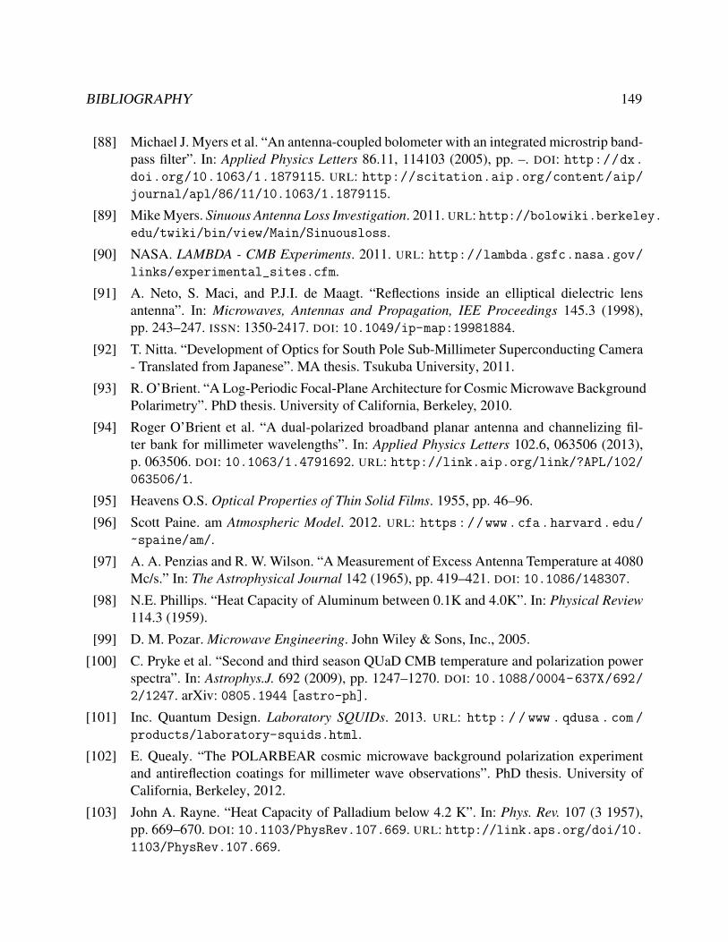
BIBLIOGRAPHY 149
[88] Michael J. Myers et al. “An antenna-coupled bolometer with an integrated microstrip band-pass filter”. In: Applied Physics Letters 86.11, 114103 (2005), pp. –. DOI: http://dx.doi.org/10.1063/1.1879115. URL: http://scitation.aip.org/content/aip/journal/apl/86/11/10.1063/1.1879115.
[89] Mike Myers. Sinuous Antenna Loss Investigation. 2011. URL: http://bolowiki.berkeley.edu/twiki/bin/view/Main/Sinuousloss.
[90] NASA. LAMBDA - CMB Experiments. 2011. URL: http://lambda.gsfc.nasa.gov/links/experimental_sites.cfm.
[91] A. Neto, S. Maci, and P.J.I. de Maagt. “Reflections inside an elliptical dielectric lensantenna”. In: Microwaves, Antennas and Propagation, IEE Proceedings 145.3 (1998),pp. 243–247. ISSN: 1350-2417. DOI: 10.1049/ip-map:19981884.
[92] T. Nitta. “Development of Optics for South Pole Sub-Millimeter Superconducting Camera- Translated from Japanese”. MA thesis. Tsukuba University, 2011.
[93] R. O’Brient. “A Log-Periodic Focal-Plane Architecture for Cosmic Microwave BackgroundPolarimetry”. PhD thesis. University of California, Berkeley, 2010.
[94] Roger O’Brient et al. “A dual-polarized broadband planar antenna and channelizing fil-ter bank for millimeter wavelengths”. In: Applied Physics Letters 102.6, 063506 (2013),p. 063506. DOI: 10.1063/1.4791692. URL: http://link.aip.org/link/?APL/102/063506/1.
[95] Heavens O.S. Optical Properties of Thin Solid Films. 1955, pp. 46–96.
[96] Scott Paine. am Atmospheric Model. 2012. URL: https://www.cfa.harvard.edu/~spaine/am/.
[97] A. A. Penzias and R. W. Wilson. “A Measurement of Excess Antenna Temperature at 4080Mc/s.” In: The Astrophysical Journal 142 (1965), pp. 419–421. DOI: 10.1086/148307.
[98] N.E. Phillips. “Heat Capacity of Aluminum between 0.1K and 4.0K”. In: Physical Review114.3 (1959).
[99] D. M. Pozar. Microwave Engineering. John Wiley & Sons, Inc., 2005.
[100] C. Pryke et al. “Second and third season QUaD CMB temperature and polarization powerspectra”. In: Astrophys.J. 692 (2009), pp. 1247–1270. DOI: 10.1088/0004-637X/692/2/1247. arXiv: 0805.1944 [astro-ph].
[101] Inc. Quantum Design. Laboratory SQUIDs. 2013. URL: http : / / www . qdusa . com /products/laboratory-squids.html.
[102] E. Quealy. “The POLARBEAR cosmic microwave background polarization experimentand antireflection coatings for millimeter wave observations”. PhD thesis. University ofCalifornia, Berkeley, 2012.
[103] John A. Rayne. “Heat Capacity of Palladium below 4.2 K”. In: Phys. Rev. 107 (3 1957),pp. 669–670. DOI: 10.1103/PhysRev.107.669. URL: http://link.aps.org/doi/10.1103/PhysRev.107.669.
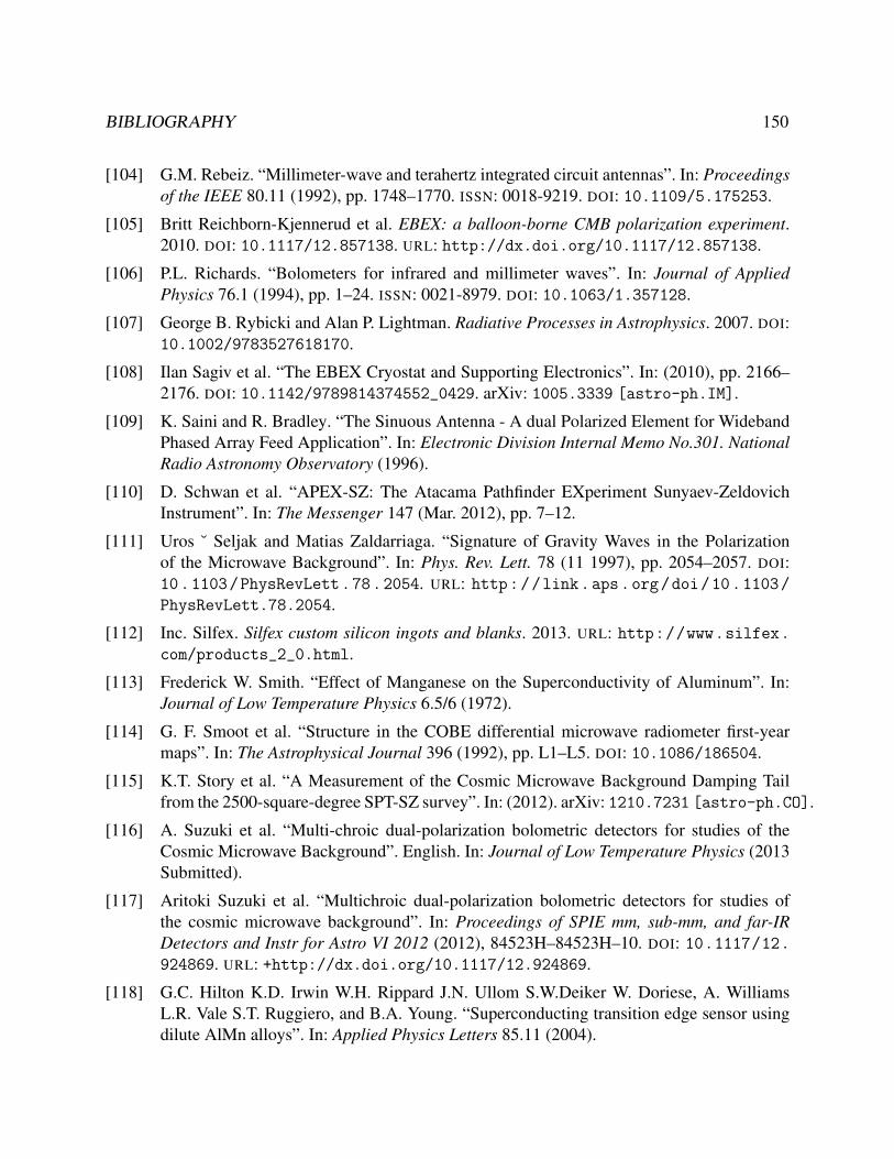
BIBLIOGRAPHY 150
[104] G.M. Rebeiz. “Millimeter-wave and terahertz integrated circuit antennas”. In: Proceedingsof the IEEE 80.11 (1992), pp. 1748–1770. ISSN: 0018-9219. DOI: 10.1109/5.175253.
[105] Britt Reichborn-Kjennerud et al. EBEX: a balloon-borne CMB polarization experiment.2010. DOI: 10.1117/12.857138. URL: http://dx.doi.org/10.1117/12.857138.
[106] P.L. Richards. “Bolometers for infrared and millimeter waves”. In: Journal of AppliedPhysics 76.1 (1994), pp. 1–24. ISSN: 0021-8979. DOI: 10.1063/1.357128.
[107] George B. Rybicki and Alan P. Lightman. Radiative Processes in Astrophysics. 2007. DOI:10.1002/9783527618170.
[108] Ilan Sagiv et al. “The EBEX Cryostat and Supporting Electronics”. In: (2010), pp. 2166–2176. DOI: 10.1142/9789814374552_0429. arXiv: 1005.3339 [astro-ph.IM].
[109] K. Saini and R. Bradley. “The Sinuous Antenna - A dual Polarized Element for WidebandPhased Array Feed Application”. In: Electronic Division Internal Memo No.301. NationalRadio Astronomy Observatory (1996).
[110] D. Schwan et al. “APEX-SZ: The Atacama Pathfinder EXperiment Sunyaev-ZeldovichInstrument”. In: The Messenger 147 (Mar. 2012), pp. 7–12.
[111] Uros ˘ Seljak and Matias Zaldarriaga. “Signature of Gravity Waves in the Polarizationof the Microwave Background”. In: Phys. Rev. Lett. 78 (11 1997), pp. 2054–2057. DOI:10.1103/PhysRevLett.78.2054. URL: http://link.aps.org/doi/10.1103/PhysRevLett.78.2054.
[112] Inc. Silfex. Silfex custom silicon ingots and blanks. 2013. URL: http://www.silfex.com/products_2_0.html.
[113] Frederick W. Smith. “Effect of Manganese on the Superconductivity of Aluminum”. In:Journal of Low Temperature Physics 6.5/6 (1972).
[114] G. F. Smoot et al. “Structure in the COBE differential microwave radiometer first-yearmaps”. In: The Astrophysical Journal 396 (1992), pp. L1–L5. DOI: 10.1086/186504.
[115] K.T. Story et al. “A Measurement of the Cosmic Microwave Background Damping Tailfrom the 2500-square-degree SPT-SZ survey”. In: (2012). arXiv: 1210.7231 [astro-ph.CO].
[116] A. Suzuki et al. “Multi-chroic dual-polarization bolometric detectors for studies of theCosmic Microwave Background”. English. In: Journal of Low Temperature Physics (2013Submitted).
[117] Aritoki Suzuki et al. “Multichroic dual-polarization bolometric detectors for studies ofthe cosmic microwave background”. In: Proceedings of SPIE mm, sub-mm, and far-IRDetectors and Instr for Astro VI 2012 (2012), 84523H–84523H–10. DOI: 10.1117/12.924869. URL: +http://dx.doi.org/10.1117/12.924869.
[118] G.C. Hilton K.D. Irwin W.H. Rippard J.N. Ullom S.W.Deiker W. Doriese, A. WilliamsL.R. Vale S.T. Ruggiero, and B.A. Young. “Superconducting transition edge sensor usingdilute AlMn alloys”. In: Applied Physics Letters 85.11 (2004).

BIBLIOGRAPHY 151
[119] Y. Sekimoto K. Mitsui N. Okada K. Karatsu M. Naruse M. Sekine H. Matsuo T. NoguchiT. Nitta S. Sekiguchi and M. Seta. Anti-Reflection (AR) Coating for Cryogenic Silicon andAlumina Lenses at Millimeter-Wave Bands. 2013.
[120] Yuki Takahashi. Ground Shields for BICEP. 2009. URL: http://bicep.caltech.edu/~yuki/shield/.
[121] APEX Web Team. Atacama Pathfinder EXperiment APEX Weather monitor. 2013. URL:http://www.apex-telescope.org/weather/.
[122] “The POLARBEAR-2 Experiment,” in: Journal of Low Temperature Physics (2013 Sub-mitted).
[123] “The POLARBEAR Cosmic Microwave Background Polarization Experiment,” in: Jour-nal of Low Temperature Physics (2013 Submitted).
[124] “Thermal conductivity and specific heat of glass ceramics”. In: ().
[125] Takayuki Tomaru et al. “The POLARBEAR-2 experiment”. In: Proceedings of SPIE mm,sub-mm, and far-IR Detectors and Instr for Astro VI 2012 (2012), 84521H–84521H–10.DOI: 10.1117/12.926158. URL: +http://dx.doi.org/10.1117/12.926158.
[126] C. E. Tucker and P. A. R. Ade. Thermal filtering for large aperture cryogenic detectorarrays. 2006.
[127] M. Pantaleev V. Belitsky C. Risacher and V. Vassilev. “Improving Accuracy of Supercon-ducting Microstrip Line Modelling at Millimetre and Sub-Millimetre Waves”. 2008. URL:https://science.nrao.edu/facilities/alma/aboutALMA/Technology/ALMA_
Memo_Series/alma533/abs533.
[128] Eric W. Weisstein. Beamsplitter. 1999. URL: http://www.ericweisstein.com/research/thesis/node19.html.
[129] Martin J. White and Mark Srednicki. “Window functions for CMB experiments”. In: Astro-phys.J. 443 (1995), p. 6. DOI: 10.1086/175497. arXiv: astro-ph/9402037 [astro-ph].
[130] J.P. Daniel X. Begaud P. Poey and G. Dubost. Design of Wideband Dual Polarized SlotAntenna. 2000.
[131] G Yassin and S Withington. “Electromagnetic models for superconducting millimetre-wave and sub-millimetre-wave microstrip transmission lines”. In: Journal of Physics D:Applied Physics 28.9 (1995), p. 1983. URL: http://stacks.iop.org/0022-3727/28/i=9/a=028.
[132] M.P. Zaitlin. “Discountinuity in the Heat Capacity of a Normal Metal-Superconductor Bi-layer”. In: Solid State Communications 41.4 (1982), pp. 317–320.
[133] J. Zhang et al. “New artificial dielectric metamaterial and its application as a terahertzantireflection coating”. In: Appl. Opt. 48.35 (2009), pp. 6635–6642. DOI: 10.1364/AO.48.006635. URL: http://ao.osa.org/abstract.cfm?URI=ao-48-35-6635.
Related Documents