TVP7002 www.ti.com SLES206C – MAY 2007 – REVISED APRIL 2013 TRIPLE 8-/10-BIT 165-/110-MSPS VIDEO AND GRAPHICS DIGITIZER WITH HORIZONTAL PLL Check for Samples: TVP7002 1FEATURES 23• Analog Channels • Output Formatter – –6-dB to 6-dB Analog Gain – Supports 20-bit 4:2:2 Outputs With Embedded Syncs – Analog Input Multiplexers (MUXs) – Support for RGB/YCbCr 4:4:4 and YCbCr – Automatic Video Clamp 4:2:2 Output Modes to Reduce Board – Three Digitizing Channels, Each With Traces Independently Controllable Clamp, Gain, – Dedicated DATACLK Output With Offset, and Analog-to-Digital Converter Programmable Output Polarity for Easy (ADC) Latching of Output Data – Clamping: Selectable Clamping Between • System Bottom Level and Mid Level – Industry-Standard Normal/Fast I 2 C Interface – Offset: 1024-Step Programmable RGB or With Register Readback Capability YPbPr Offset Control – Space-Saving 100-Pin TQFP Package – Gain: 8-Bit Programmable Gain Control – Thermally-Enhanced PowerPAD™ Package – ADC: 8-/10-Bit 165-/110-MSPS ADC for Better Heat Dissipation – Automatic Level Control (ALC) Circuit – Composite Sync: Integrated Sync-on-Green APPLICATIONS Extraction From Green/Luminance Channel • LCD TVs/Monitors/Projectors – Support for DC- and AC-Coupled Input • DLP TVs/Projectors Signals • PDP TVs/Monitors – Supports Component Video Standards 480i, • LCOS TVs/Monitors 576i, 480p, 576p, 720p, 1080i, and 1080p • PCTV Set-Top Boxes – Supports PC Graphics Inputs up to UXGA • Digital Image Processing – Programmable RGB-to-YCbCr Color Space Conversion • Video Capture/Video Editing • Horizontal PLL • Scan Rate/Image Resolution Converters – Fully Integrated Horizontal PLL for Pixel • Video Conferencing Clock Generation • Video/Graphics Digitizing Equipment – 12-MHz to 165-MHz Pixel Clock Generation From HSYNC Input – Adjustable Horizontal PLL Loop Bandwidth for Minimum Jitter – 5-Bit Programmable Subpixel Accurate Positioning of Sampling Phase DESCRIPTION The TVP7002 is a complete solution for digitizing video and graphic signals in RGB or YPbPr color spaces. The device supports pixel rates up to 165 MHz. Therefore, it can be used for PC graphics digitizing up to the VESA standard of UXGA (1600 × 1200) resolution at a 60-Hz screen refresh rate, and in video environments for the digitizing of digital TV formats, including HDTV up to 1080p. 1 Please be aware that an important notice concerning availability, standard warranty, and use in critical applications of Texas Instruments semiconductor products and disclaimers thereto appears at the end of this data sheet. 2PowerPAD is a trademark of Texas Instruments. 3All other trademarks are the property of their respective owners. PRODUCTION DATA information is current as of publication date. Copyright © 2007–2013, Texas Instruments Incorporated Products conform to specifications per the terms of the Texas Instruments standard warranty. Production processing does not necessarily include testing of all parameters.

Welcome message from author
This document is posted to help you gain knowledge. Please leave a comment to let me know what you think about it! Share it to your friends and learn new things together.
Transcript

TVP7002
www.ti.com SLES206C –MAY 2007–REVISED APRIL 2013
TRIPLE 8-/10-BIT 165-/110-MSPSVIDEO AND GRAPHICS DIGITIZER WITH HORIZONTAL PLL
Check for Samples: TVP7002
1FEATURES23• Analog Channels • Output Formatter
– –6-dB to 6-dB Analog Gain – Supports 20-bit 4:2:2 Outputs WithEmbedded Syncs– Analog Input Multiplexers (MUXs)
– Support for RGB/YCbCr 4:4:4 and YCbCr– Automatic Video Clamp4:2:2 Output Modes to Reduce Board– Three Digitizing Channels, Each WithTracesIndependently Controllable Clamp, Gain,
– Dedicated DATACLK Output WithOffset, and Analog-to-Digital ConverterProgrammable Output Polarity for Easy(ADC)Latching of Output Data– Clamping: Selectable Clamping Between
• SystemBottom Level and Mid Level– Industry-Standard Normal/Fast I2C Interface– Offset: 1024-Step Programmable RGB or
With Register Readback CapabilityYPbPr Offset Control– Space-Saving 100-Pin TQFP Package– Gain: 8-Bit Programmable Gain Control– Thermally-Enhanced PowerPAD™ Package– ADC: 8-/10-Bit 165-/110-MSPS ADC
for Better Heat Dissipation– Automatic Level Control (ALC) Circuit– Composite Sync: Integrated Sync-on-Green APPLICATIONS
Extraction From Green/Luminance Channel• LCD TVs/Monitors/Projectors– Support for DC- and AC-Coupled Input• DLP TVs/ProjectorsSignals• PDP TVs/Monitors– Supports Component Video Standards 480i,• LCOS TVs/Monitors576i, 480p, 576p, 720p, 1080i, and 1080p• PCTV Set-Top Boxes– Supports PC Graphics Inputs up to UXGA• Digital Image Processing– Programmable RGB-to-YCbCr Color
Space Conversion • Video Capture/Video Editing• Horizontal PLL • Scan Rate/Image Resolution Converters
– Fully Integrated Horizontal PLL for Pixel • Video ConferencingClock Generation • Video/Graphics Digitizing Equipment
– 12-MHz to 165-MHz Pixel Clock GenerationFrom HSYNC Input
– Adjustable Horizontal PLL Loop Bandwidthfor Minimum Jitter
– 5-Bit Programmable Subpixel AccuratePositioning of Sampling Phase
DESCRIPTIONThe TVP7002 is a complete solution for digitizing video and graphic signals in RGB or YPbPr color spaces. Thedevice supports pixel rates up to 165 MHz. Therefore, it can be used for PC graphics digitizing up to the VESAstandard of UXGA (1600 × 1200) resolution at a 60-Hz screen refresh rate, and in video environments for thedigitizing of digital TV formats, including HDTV up to 1080p.
1
Please be aware that an important notice concerning availability, standard warranty, and use in critical applications ofTexas Instruments semiconductor products and disclaimers thereto appears at the end of this data sheet.
2PowerPAD is a trademark of Texas Instruments.3All other trademarks are the property of their respective owners.
PRODUCTION DATA information is current as of publication date. Copyright © 2007–2013, Texas Instruments IncorporatedProducts conform to specifications per the terms of the TexasInstruments standard warranty. Production processing does notnecessarily include testing of all parameters.

Output
Formatter
R[9:0]
G[9:0]
Host
Interface
Timing Processor
and
Clock Generation
RIN_1
SCL
SDA
I2CA
GIN_1
BIN_1
Clamp
Clamp
Clamp
Gain andOffset
10-bitADC
HSYNC_A
VSYNC_A
COAST
CLAMP
FILT1
SOGIN_1
RESETB
PWDN
B[9:0]
SOGOUT
HSOUT
VSOUT
DATACLK
RIN_2
GIN_2
BIN_2
EXT_CLK
SOGIN_2
HSYNC_B
VSYNC_B
FILT2
RIN_3
GIN_3
GIN_4
SOGIN_3
BIN_3
FIDOUT
Color Space
Conversion
and
4:4:4 to 4:2:2
Conversion
Gain andOffset
Gain andOffset
10-bitADC
10-bitADC
TVP7002
SLES206C –MAY 2007–REVISED APRIL 2013 www.ti.com
The TVP7002 is powered from 3.3-V and 1.9-V supply and integrates a triple high-performance analog-to-digital(A/D) converter with clamping functions and variable gain, independently programmable for each channel. Theclamp timing window is provided by an external pulse or can be generated internally. The TVP7002 includesanalog slicing circuitry on the SOG inputs to support sync-on-luminance or sync-on-green extraction. In addition,TVP7002 can extract discrete HSYNC and VSYNC from composite sync using a sync slicer.
The TVP7002 also contains a complete horizontal phase-locked loop (PLL) block to generate a pixel clock fromthe HSYNC input. Pixel clock output frequencies range from 12 MHz to 165 MHz.
All programming of the device is done via an industry-standard I2C interface, which supports both reading andwriting of register settings. The TVP7002 is available in a space-saving 100-pin TQFP PowerPAD package.
Ordering Information (1)
PACKAGED DEVICESTA PACKAGE OPTION
100-PIN PLASTIC FLATPACK PowerPAD
TVP7002PZP Tray0°C to 70°C
TVP7002PZPR Reel
(1) For the most current package and ordering information, see the Package Option Addendum at the endof this document, or see the TI web site at www.ti.com.
Functional Block Diagram
2 Submit Documentation Feedback Copyright © 2007–2013, Texas Instruments Incorporated
Product Folder Links: TVP7002

TVP7002100-Pin TQFP Package
(Top View)
10
0G
IN_2
99
SO
GIN
_2
98
GIN
_3
97
SO
GIN
_3
96
GIN
_4
95
A33G
ND
94
A33V
DD
93
A33V
DD
92
A33G
ND
91
NS
UB
90
PLL_A
GN
D
89
PLL_F
88
FIL
T2
87
FIL
T1
86
PLL_A
GN
D
85
PLL_A
VD
D
84
PLL_A
VD
D
83
PLL_A
GN
D
82
HS
YN
C_B
81
HS
YN
C_A
80
EX
T_C
LK
79
VS
YN
C_B
78
VS
YN
C_A
77
CO
AS
T
76
CLA
MP
26
IOV
DD
27
IOG
ND
28
DATA
CLK
29
B_9
30
B_8
31
B_7
32
B_6
33
B_5
34
B_4
35
B_3
36
B_2
37
B_1
38
B_0
39
DV
DD
40
GN
D
41
IOV
DD
42
IOG
ND
43
G_9
44
G_8
45
G_7
46
G_6
47
G_5
48
G_4
49
G_3
50
G_2
75 SDA
74 SCL
73 I2CA
72 TMS
71 RESETB
70 PWDN
69 DVDD
68 GND
67 IOGND
66 IOVDD
65 R_0
64 R_1
63 R_2
62 R_3
61 R_4
60 IOGND
59 R_5
58 R_6
57 R_7
56 R_8
55 R_9
54 IOGND
53 IOVDD
52 G_0
51 G_1
1SOGIN_1
2GIN_1
3AGND
4AVDD
5A DGN
6AVDD
7AVDD
8AGND
9RI _N 3
10RIN_2
11RIN_1
12A33GND
13A33VDD
14A33VDD
15A33GND
16BIN_3
17BIN_2
18BIN_1
19AV DD
20AGND
21NSUB
22FIDOUT
23VSOUT
24HSOUT
25SOGOUT
TVP7002
www.ti.com SLES206C –MAY 2007–REVISED APRIL 2013
Terminal Assignments
Copyright © 2007–2013, Texas Instruments Incorporated Submit Documentation Feedback 3
Product Folder Links: TVP7002

TVP7002
SLES206C –MAY 2007–REVISED APRIL 2013 www.ti.com
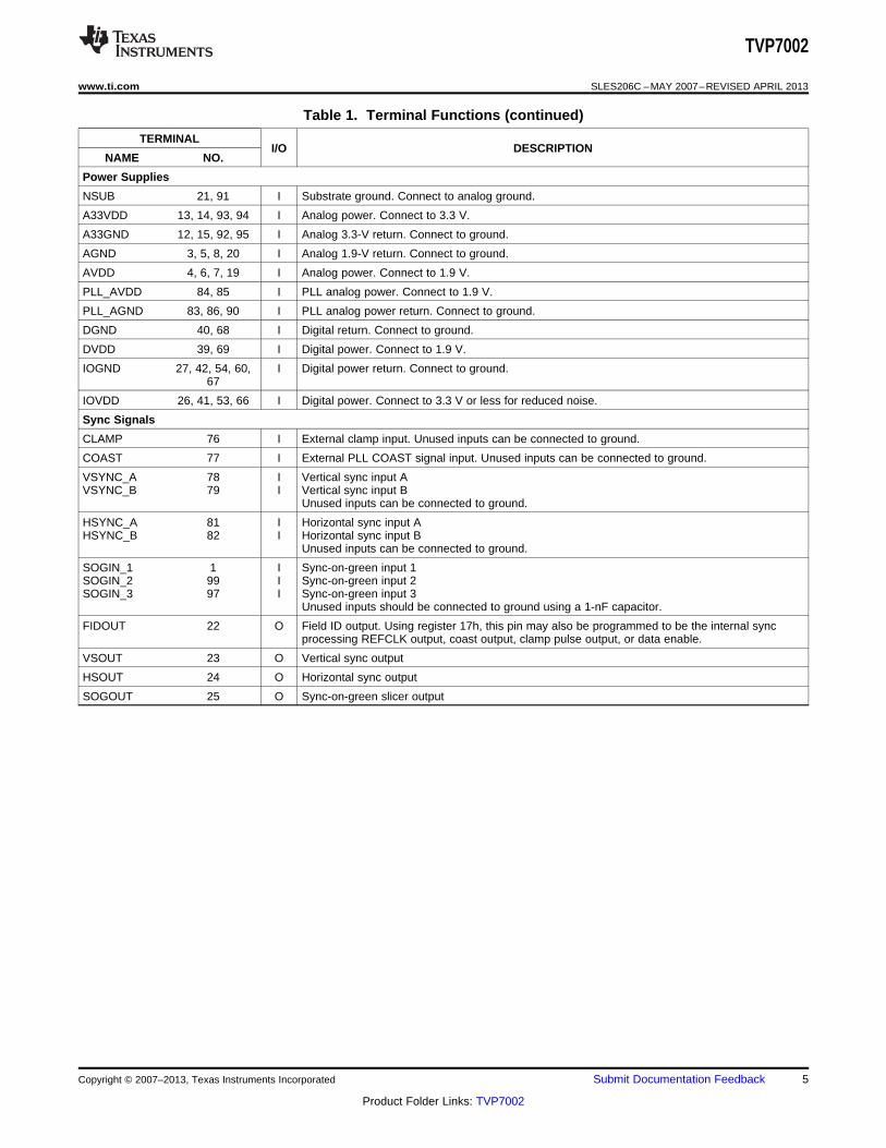
Table 1. Terminal Functions
TERMINALI/O DESCRIPTION
NAME NO.
Analog Video
RIN_1 11 I Analog video input for R/Pr 1RIN_2 10 I Analog video input for R/Pr 2RIN_3 9 I Analog video input for R/Pr 3GIN_1 2 I Analog video input for G/Y 1GIN_2 100 I Analog video input for G/Y 2GIN_3 98 I Analog video input for G/Y 3GIN_4 96 I Analog video input for G/Y 4BIN_1 18 I Analog video input for B/Pb 1BIN_2 17 I Analog video input for B/Pb 2BIN_3 16 I Analog video input for B/Pb 3
The inputs must be ac coupled. The recommended coupling capacitor is 0.1 μF. Unused analoginputs should be connected to ground using a 10-nF capacitor.
Clock Signals
DATACLK 28 O Data clock output
EXT_CLK 80 I External clock input. May be used as a timing reference for the mode detection block instead ofthe internal clock reference. May also be used as the ADC sample clock instead of the H-PLLgenerated clock.
Digital Video
R[9:0] 55–59, 61–65 O Digital video output of R/Cr, R[9] is the most significant bit (MSB).G[9:0] 43-52 O Digital video output of G/Y, G[9] is the MSB.B[9:0] 29-38 O Digital video output of B/Cb, B[9] is the MSB.
For 4:2:2 mode, multiplexed CbCr data is output on B[9:0].Unused outputs can be left unconnected.
Miscellaneous Signals
PWDN 70 I Power down input0 = Normal mode1 = Power down
RESETB 71 I Reset input, active low. Outputs are placed in a high-impedance mode during reset (seeTable 11).
TMS 72 I Test mode select input, active high. Used to enable scan test mode. For normal operation,connect to ground.
FILT1 87 O External filter connection for the horizontal PLL. A 0.1-μF capacitor in series with a 1.5-kΩresistor should be connected from this pin to pin 89 (see Figure 4).
FILT2 88 O External filter connection for the horizontal PLL. A 4.7-nF capacitor should be connected fromthis pin to pin 89 (see Figure 4).
PLL_F 89 I Horizontal PLL filter internal supply connection
Host Interface
I2CA 73 I I2C slave address input. The I2C slave address must be configured with an external pullup orpulldown resistor (see Table 10).0 = Slave address = B8h1 = Slave address = BAh
SCL 74 I I2C clock input
SDA 75 I/O I2C data bus
4 Submit Documentation Feedback Copyright © 2007–2013, Texas Instruments Incorporated
Product Folder Links: TVP7002
TVP7002
www.ti.com SLES206C –MAY 2007–REVISED APRIL 2013
Table 1. Terminal Functions (continued)
TERMINALI/O DESCRIPTION
NAME NO.
Power Supplies
NSUB 21, 91 I Substrate ground. Connect to analog ground.
A33VDD 13, 14, 93, 94 I Analog power. Connect to 3.3 V.
A33GND 12, 15, 92, 95 I Analog 3.3-V return. Connect to ground.
AGND 3, 5, 8, 20 I Analog 1.9-V return. Connect to ground.
AVDD 4, 6, 7, 19 I Analog power. Connect to 1.9 V.
PLL_AVDD 84, 85 I PLL analog power. Connect to 1.9 V.
PLL_AGND 83, 86, 90 I PLL analog power return. Connect to ground.
DGND 40, 68 I Digital return. Connect to ground.
DVDD 39, 69 I Digital power. Connect to 1.9 V.
IOGND 27, 42, 54, 60, I Digital power return. Connect to ground.67
IOVDD 26, 41, 53, 66 I Digital power. Connect to 3.3 V or less for reduced noise.
Sync Signals
CLAMP 76 I External clamp input. Unused inputs can be connected to ground.
COAST 77 I External PLL COAST signal input. Unused inputs can be connected to ground.
VSYNC_A 78 I Vertical sync input AVSYNC_B 79 I Vertical sync input B
Unused inputs can be connected to ground.
HSYNC_A 81 I Horizontal sync input AHSYNC_B 82 I Horizontal sync input B
Unused inputs can be connected to ground.
SOGIN_1 1 I Sync-on-green input 1SOGIN_2 99 I Sync-on-green input 2SOGIN_3 97 I Sync-on-green input 3
Unused inputs should be connected to ground using a 1-nF capacitor.
FIDOUT 22 O Field ID output. Using register 17h, this pin may also be programmed to be the internal syncprocessing REFCLK output, coast output, clamp pulse output, or data enable.
VSOUT 23 O Vertical sync output
HSOUT 24 O Horizontal sync output
SOGOUT 25 O Sync-on-green slicer output
Copyright © 2007–2013, Texas Instruments Incorporated Submit Documentation Feedback 5
Product Folder Links: TVP7002

TVP7002
SLES206C –MAY 2007–REVISED APRIL 2013 www.ti.com
Absolute Maximum Ratings (1)
over operating free-air temperature range (unless otherwise noted)
IOVDD to IOGND –0.5 V to 4.5 V
DVDD to DGND –0.5 V to 2.3 VSupply voltage range
PLL_AVDD to PLL_AGND and AVDD to AGND –0.5 V to 2.3 V
A33VDD to A33GND –0.5 V to 4.5 V
Digital input voltage range VI to DGND –0.5 V to 4.5 V
Analog input voltage range AI to A33GND –0.2 V to 2.3 V
Digital output voltage range VO to DGND –0.5 V to 4.5 V
TA Operating free-air temperature range 0°C to 70°C
Tstg Storage temperature range –65°C to 150°C
(1) Stresses beyond those listed under Absolute Maximum Ratings may cause permanent damage to the device. These are stress ratingsonly and functional operation of the device at these or any other conditions beyond those indicated under Recommended OperatingConditions is not implied. Exposure to absolute-maximum-rated conditions for extended periods may affect device reliability.
Thermal SpecificationsPARAMETER TEST CONDITIONS (1) MIN TYP MAX UNIT
θJA Junction-to-ambient thermal resistance, still air Thermal pad soldered to 4-layer 17.28 °C/WHigh-K PCB
θJC Junction-to-case thermal resistance, still air Thermal pad soldered to 4-layer 0.154 °C/WHigh-K PCB
TJ(MAX) Maximum junction temperature for reliable operation 110 °C
(1) Exposed thermal pad must be soldered to JEDEC High-K PCB with adequate ground plane. If split ground planes are used, connect thethermal pad to the digital ground plane.
Recommended Operating ConditionsMIN NOM MAX UNIT
IOVDD Digital I/O supply voltage 3 3.3 3.6 V
DVDD Digital supply voltage 1.8 1.9 2 V
PLL_AVDD Analog supply voltage for horizontal PLL 1.8 1.9 2 V
AVDD Analog supply voltage 1.8 1.9 2 V
A33VDD Analog supply voltage 3 3.3 3.6 V
VI(P-P) Analog input voltage (ac coupling necessary) 0.5 2 V
VIH Digital input voltage high 0.7 IOVDD V
VIL Digital input voltage low 0.3 IOVDD V
IOH High-level output current 2 mA
IOL Low-level output current –2 mA
IOH_DATACLK DATACLK high-level output current 4 mA
IOL_DATACLK DATACLK low-level output current –4 mA
ADC conversion rate 12 162 MHz
TA Operating free-air temperature 0 70 °C
6 Submit Documentation Feedback Copyright © 2007–2013, Texas Instruments Incorporated
Product Folder Links: TVP7002

TVP7002
www.ti.com SLES206C –MAY 2007–REVISED APRIL 2013
Electrical CharacteristicsIOVDD = 3.3 V, DVDD = 1.9 V, PLL_AVDD = 1.9 V, AVDD = 1.9 V, A33VDD = 3.3 V, TA = 25°C
PARAMETER TEST CONDITIONS (1) TYP (2) TYP (3) UNIT
Power Supply
IA33VDD 3.3-V supply current 78.75 MHz, BC = 5 67 67 mA
IIOVDD 3.3-V supply current 78.75 MHz, BC = 5 21 56 mA
IAVDD 1.9-V supply current 78.75 MHz, BC = 5 206 209 mA
IPLL_VDD 1.9-V supply current 78.75 MHz, BC = 5 16 16 mA
IDVDD 1.9-V supply current 78.75 MHz, BC = 5 30 46 mA
PTOT Total power dissipation, normal mode 78.75 MHz, BC = 5 743 893 mW
IA33VDD 3.3-V supply current 162 MHz, BC = 8 110 110 mA
IIOVDD 3.3-V supply current 162 MHz, BC = 8 35 102 mA
IAVDD 1.9-V supply current 162 MHz, BC = 8 275 279 mA
IPLL_VDD 1.9-V supply current 162 MHz, BC = 8 22 23 mA
IDVDD 1.9-V supply current 162 MHz, BC = 8 56 89 mA
PTOT Total power dissipation, normal mode 162 MHz, BC = 8 1112 1403 mW
PDOWN Total power dissipation, power-down mode 15 15 mW
(1) BC = ADC bias control setting in I2C register, 2Ch(2) SMPTE color bar RGB input pattern used(3) Worst-case vertical line RGB input pattern used
Copyright © 2007–2013, Texas Instruments Incorporated Submit Documentation Feedback 7
Product Folder Links: TVP7002

TVP7002
SLES206C –MAY 2007–REVISED APRIL 2013 www.ti.com
Electrical CharacteristicsIOVDD = 3.3 V, DVDD = 1.9 V, PLL_AVDD = 1.9 V, AVDD = 1.9 V, A33VDD = 3.3 V, TA = 0°C to 70°C (unless otherwisenoted)
PARAMETER TEST CONDITIONS (1) MIN TYP MAX UNIT
Analog Interface
Input voltage range By design 0.5 1 2 Vpp
ZI Input impedance, analog video inputs By design 500 kΩDigital Logic Interface
CI Input capacitance By design 10 pF
ZI Input impedance By design 500 kΩVOH Output voltage high IOH = 2 mA 0.8 IOVDD V
VOL Output voltage low IOL = –2 mA 0.2 IOVDD V
VOH_SCLK DATACLK output voltage high IOH = 4 mA 0.8 IOVDD V
VOL_SCLK DATACLK output voltage low IOH = –4 mA 0.2 IOVDD V
VIH High-level input voltage By design 0.7 IOVDD V
VIL Low-level input voltage By design 0.3 IOVDD V
ADCs
ADC full-scale input range Clamp disabled 0.95 1 1.05 Vpp
ADC resolution 10-bit range 10 bits
10 bit, 110 MHz, BC = 5 –1 ±0.5 +1DNL DC differential nonlinearity LSB
8 bit, 162 MHz, BC = 8 –1 ±0.5 +1
10 bit, 110 MHz, BC = 5 –4 ±1 +4INL DC integral nonlinearity LSB
8 bit, 162 MHz, BC = 8 –4 ±1 +4
10 bit, 110 MHz, BC = 5 noneMissing code
8 bit, 162 MHz, BC = 8 none
SNR Signal-to-noise ratio 10 MHz, 1 VP-P at 110 MSPS 55 dB
Analog 3-dB bandwidth By design 350 500 MHz
Horizontal PLL
Clock jitter 500 ps
Phase adjustment 11.6 degree
VCO frequency range By design 12 162 MHz
Analog ADC Channel
Coarse gain full-scale control range Gain control value NG = 15 ±6 dB
Coarse offset full-scale control range Referred to 10-bit ADC output ±124 counts
Coarse offset step size Referred to 10-bit ADC output 4 counts
Sync Processing
Internal clock reference frequency By design 6.5 MHz
(1) BC = ADC bias control setting in I2C register, 2Ch
8 Submit Documentation Feedback Copyright © 2007–2013, Texas Instruments Incorporated
Product Folder Links: TVP7002

DATACLK
t1
t2
t3
Valid DataR, G, B, HSOUT Valid Data
VOH
VOL
CLK POL = 0
CLK POL = 1
TVP7002
www.ti.com SLES206C –MAY 2007–REVISED APRIL 2013
Timing RequirementsPARAMETER TEST CONDITIONS (1) MIN TYP MAX UNIT
Clocks, Video Data, Sync Timing
Positive duty cycle, DATACLK (CLK POL = 0) 48 50 52 %
Positive duty cycle, DATACLK (CLK POL = 1) 41 43 45 %
t1 DATACLK rise time 10% to 90% 1 ns
t2 DATACLK fall time 90% to 10% 1 ns
t3 (RGB data) RGB output delay time 0 1.5 ns
(1) Measured at 162 MHz with 22-Ω series termination resistor and 10-pF load. Specified by characterization only. Data is clocked out onthe rising edge of DATACLK with Reg 18h CLK POL=0 and is clocked out on the falling edge of DATACLK with CLK POL=1.
Figure 1. Clock, Video Data, and HSOUT Timing
Copyright © 2007–2013, Texas Instruments Incorporated Submit Documentation Feedback 9
Product Folder Links: TVP7002

SDA
t1t6
t7t2
t8
t3t4
t6
SCL
Data
Stop Start Stop
t5
TVP7002
SLES206C –MAY 2007–REVISED APRIL 2013 www.ti.com
Timing RequirementsPARAMETER TEST CONDITIONS MIN TYP MAX UNIT
I2C Host Port
t1 Bus free time between Stop and Start Specified by design 1.3 μs
t2 Setup time for a (repeated) Start condition Specified by design 0.6 μs
t3 Hold time (repeated) Start condition Specified by design 0.6 μs
t4 Setup time for a Stop condition Specified by design 0.6 ns
t5 Data setup time Specified by design 100 ns
t6 Data hold time Specified by design 0 0.9 μs
t7 Rise time, SDA and SCL signal Specified by design 250 ns
t8 Fall time, SDA and SCL signal Specified by design 250 ns
Cb Capacitive load for each bus line Specified by design 400 pF
fI2C I2C clock frequency Specified by design 400 kHz
Figure 2. I2C Host Port Timing
10 Submit Documentation Feedback Copyright © 2007–2013, Texas Instruments Incorporated
Product Folder Links: TVP7002

TVP7002
www.ti.com SLES206C –MAY 2007–REVISED APRIL 2013
FUNCTIONAL DESCRIPTION
Analog Channel
The TVP7002 contains three identical analog channels that are independently programmable. Each channelconsists of a clamping circuit, programmable gain control, programmable offset control, and an ADC.
Analog Input Switch Control
TVP7002 has three analog channels that accept up to ten video inputs. The user can configure the internalanalog video switches via the I2C interface. The ten analog video inputs can be used for different inputconfigurations, some of which are:• Up to three SDTV, EDTV, or HDTV component video inputs (limited by number of SOG inputs)• Up to two 5-wire PC graphics inputs (limited by number of HSYNC and VSYNC inputs)
The input selection is performed by the input select register at I2C subaddress 19h a 1Ah (see InputMux Select 1 and Input Mux Select 2).
Supported Video Formats
The TVP7002 supports A/D conversion of SDTV (480i, 576i), EDTV (480p, 576p), and HDTV (720p, 1080i,1080p) YPbPr component video inputs. The TVP7002 also supports A/D conversion and color space conversionof all standard PC graphics formats (RGB) from VGA up to UXGA. The internal sync separator provides supportfor field rates (VSYNC frequencies) at or above 40 Hz. Separated VSYNC or an external sync separator must beused to support formats having field rates less than 40 Hz. A summary of the analog video standards supportedby the TVP7002 module is show in Table 2.
Table 2. Analog Video Standards
VIDEO FORMAT VIDEO STANDARDS
SDTV (YPbPr component) 480i, 576i
EDTV (YPbPr component) 480p, 576p
720p50, 720p60, 1080i50,HDTV (YPbPr component) 1080i60, 1080p50, 1080p60
PC graphics (RGB component) VGA to UXGA
SCART (RGB component) 576i
Analog Input Clamping
The TVP7002 provides dc restoration for all analog video inputs including the SOG slicer inputs. The dcrestoration circuit (a.k.a. clamp circuit) restores the ac-coupled video signal to a fixed dc level. One dc restorationcircuit is implemented prior to each of the three ADCs, and a fourth one is located prior to the SOG slicer. The dcrestoration circuit can be programmed to operate as either a sync-tip clamp (a.k.a. coarse clamp) or a back-porch clamp (a.k.a. fine clamp). The sync-tip clamp always clamps the video sync-tip level near the bottom of theADC range. The back-porch type clamp supports two clamping levels (bottom level and mid level) that areselectable using bits 0, 1, and 2 of register 10h. When using the fine bottom-level clamp, an optional 300-mVcommon-mode offset may be selected using bit 7 of register 2Ah.
In general, the analog video input being used for horizontal synchronization purposes should always use thesync-tip clamp; all other analog video inputs should use the back-porch clamp. The advantage of the back-porchclamp is that it has negligible video droop or tilt across a video line.
Copyright © 2007–2013, Texas Instruments Incorporated Submit Documentation Feedback 11
Product Folder Links: TVP7002

TVP7002
SLES206C –MAY 2007–REVISED APRIL 2013 www.ti.com
The selection between bottom- and mid-level clamping is performed by I2C subaddress 10h (see Sync-On-GreenThreshold). The fine clamps must also be enabled via I2C register 2Ah for proper operation. The internalclamping time can be adjusted using the I2C clamp start and width registers at subaddress 05h and 06h,respectively (see Clamp Start and Clamp Width).
Table 3. Recommended Clamp Setting by Video Mode
SOG INPUT GREEN ADC CHANNEL RED ADC CHANNEL BLUE ADC CHANNELVIDEO MODE (Y/G) (Y/G) (Pr/R) (Pb/B)
YPbPr component Coarse Fine Bottom Level Fine Mid Level Fine Mid Level
PC graphics Coarse Fine Bottom Level Fine Bottom Level Fine Bottom Level
SCART-RGB Coarse Fine Bottom Level Fine Bottom Level Fine Bottom Level
A single-pole low-pass filter with three selectable cutoff frequencies (0.5, 1.7, and 4.8 MHz) is implemented in thefeedback loop of the sync-tip clamp circuit.
Programmable Gain Control
The TVP7002 provides a 4-bit coarse analog gain control (before A/D conversion) and an 8-bit fine digital gaincontrol (after A/D conversion). The coarse analog gain and the fine digital gain are both independentlyprogrammable for each ADC channel.
Coarse Gain Control
The 4-bit coarse analog gain control has a 4:1 linear gain control range defined by the following equation.Coarse Gain = 0.5 + NCG/10, where 0 ≤ NCG ≤ 150.5 ≤ Coarse Gain ≤ 2.0Default: NCG = 7 (Coarse Gain = 1.2)
The 4-bit coarse gain control can scale a signal with a voltage-input compliance of 0.5 VP-P to 2 VP-P to a full-scale 10-bit A/D output code range. The minimum gain corresponds to a code 0h (2-VP-P full-scale input, –6-dBgain) while the maximum gain corresponds to code Fh (0.5-VP-P full scale, +6 dB gain). The 4-bit coarse gaincontrol is independently controllable for each ADC channel (Red Coarse Gain, Green Coarse Gain, and BlueCoarse Gain).
Fine Gain Control
The 8-bit fine digital gain control has a 2:1 linear gain control range defined by the following equation.Fine Gain = 1.0 + NFG/256 where 0 ≤ NFG ≤ 2551.0 ≤ Fine Gain < 2.0Default: NFG = 0 (Fine Gain = 1.0)
The 8-bit fine gain control is independently controllable for each ADC channel (Red Fine Gain, Green Fine Gain,and Blue Fine Gain). For a normal PC graphics input, the fine gain is used mostly.
Programmable Offset Control
The TVP7002 provides a 6-bit coarse analog offset control (before A/D conversion) and a 10-bit fine digital offsetcontrol (after A/D conversion). The coarse analog offset and the fine digital offset are both independentlyprogrammable for each ADC channel.
Coarse Offset Control
A 6-bit code sets the coarse offset (Red Coarse Offset, Green Coarse Offset, Blue Coarse Offset) with individualadjustment per channel. The coarse offset ranges from –32 counts to +31 counts. The coarse offset registersapply before the ADC.
Fine Offset Control
A 10-bit fine offset registers (Red Fine Offset, Green Fine Offset, Blue Fine Offset) apply after the ADC. The fineoffset ranges from –512 counts to +511 counts.
12 Submit Documentation Feedback Copyright © 2007–2013, Texas Instruments Incorporated
Product Folder Links: TVP7002

COAST
HSYNCPhase
Detector
PLL ControlRegister 03h
Bit [5:3]
PLL ControlRegister 03h
Bit [7:6]
Phase SelectRegister 04h
Bit [7:3]
ChargePump
VCOPhaseSelect
Divider
ADCSampling
CLK
ExternalClock
PLL DivideRegister 01h and 02h
1:0]Bit [1
LoopFilter
N = 1 or 2
PostDivider
÷N
Post DividerRegister 04h
Bit [0]
TVP7002
www.ti.com SLES206C –MAY 2007–REVISED APRIL 2013
Automatic Level Control (ALC)
The ALC circuit maintains the level of the signal to be set at a value that is programmed at the fine offset I2Cregister. It consists of a pixel averaging filter and feedback loop. This ALC function can be enabled or disabled bythe I2C register at subaddress 26h.
The ALC circuit needs a timing pulse generated internally but the user should program the position properly. TheALC pulse must be positioned after the clamp pulse. The position of ALC pulse is controlled by ALC placementI2C register at address 31h. This is available only for internal ALC pulse timing. When using an external clamppulse, the fine clamp and the ALC both start on the leading edge of the external clamp pulse. Therefore, it isrecommended to keep the external clamp pulse as long as possible.
Analog-to-Digital Converters (ADCs)
All ADCs have a resolution of 10 bits and can operate up to 165 MSPS. All A/D channels receive an identicalclock from the on-chip phase-locked loop (PLL) at a frequency between 12 MHz and 165 MHz. All ADCreference voltages are generated internally. Also the external sampling clock can be used.
Horizontal PLL
The horizontal PLL generates a high-frequency internal clock used by the ADC sampling and data clocking out toderive the pixel output frequency with programmable phase. The reference signal for this PLL is the horizontalsync signal supplied on the HSYNC input or from extracted horizontal sync of the sync slicer block for embeddedsync signals. The horizontal PLL consists of a phase detector, charge pump, loop filter, voltage controlledoscillator (VCO), phase select, feedback divider, and post divider. The horizontal PLL block diagram is shown inFigure 3.
Figure 3. Horizontal PLL Block Diagram
The COAST signal is used to allow the PLL to keep running at the same frequency, in the absence of theincoming HSYNC signal or disordered HSYNC period. This is useful during the vertical sync period, or any othertime that the HSYNC is not available.
There are several PLL controls to produce the correct sampling clock. The 12-bit feedback divider register isprogrammable to select exact multiplication number to generate the pixel clock in the range of 12 MHz to165 MHz. The 3-bit loop filter current control register is to control the charge pump current that drives the low-pass loop filter. The applicable current values are listed in the Table 4.
Copyright © 2007–2013, Texas Instruments Incorporated Submit Documentation Feedback 13
Product Folder Links: TVP7002

0.1 µF
4.7 nF
1.5 kW
TVP7002
PLL_F
FILT2
FILT1
89
88
87
TVP7002
SLES206C –MAY 2007–REVISED APRIL 2013 www.ti.com
The purpose of the 2-bit VCO range control is to improve the noise performance of the TVP7002. The frequencyranges for the VCO are shown in Table 4. The phase of the ADC sample clock generated by the horizontal PLLcan be accurately controlled in 32 uniform steps over a single clock period (360/32 = 11.25 degrees phaseresolution) using the phase select register located at subaddress 04h.
The horizontal PLL characteristics are determined by the loop filter design, the PLL charge pump current, and theVCO range setting. The loop filter design is shown in Figure 4. Supported settings of VCO range and chargepump current for VESA standard display modes are listed in Table 4.
Figure 4. Horizontal PLL Loop Filter
In addition to sourcing the ADC sample clock from the horizontal PLL, an external pixel clock can be used (frompin 80).
Table 4. Recommended VCO Range and Charge Pump Current Settingsfor Supporting Standard Display Formats
PLL VCO CPFRAME PIXEL PLLDIV PLLDIV OUTPUTLINE RATE DIVIDER RANGE CURRENTSTANDARD RESOLUTION RATE RATE [11:4] REG [3:0] REG REG 03h DIVIDER(kHz) TOTAL REG 03h REG 03h(Hz) (MHz) 01h [7:0] 02h [7:4] REG 04h [0]PIX/LINE [7:6] [5:3]
640 × 480 59.94 31.469 25.175 800 32h 00h 20h 0 ULow (00b) 100b
640 × 480 72.809 37.861 31.5 832 34h 00h 20h 0 ULow (00b) 100bVGA
640 × 480 75 37.5 31.5 840 34h 80h 20h 0 ULow (00b) 100b
640 × 480 85.008 43.269 36 832 34h 00h 60h 0 Low (01b) 100b
800 × 600 56.25 35.156 36 1024 40h 00h 58h 0 Low (01b) 011b
800 × 600 60.317 37.879 40 1056 42h 00h 58h 0 Low (01b) 011b
SVGA 800 × 600 72.188 48.077 50 1040 41h 00h 58h 0 Low (01b) 011b
800 × 600 75 46.875 49.5 1056 42h 00h 58h 0 Low (01b) 011b
800 × 600 85.061 53.674 56.25 1048 41h 80h 58h 0 Low (01b) 011b
1024 × 768 60.004 48.363 65 1344 54h 00h 58h 0 Low (01b) 011b
1024 ×768 70.069 56.476 75 1328 53h 00h A8h 0 Med (10b) 101bXGA
1024 × 768 75.029 60.023 78.75 1312 52h 00h A8h 0 Med (10b) 101b
1024 × 768 84.997 68.677 94.5 1376 56h 00h A0h 0 Med (10b) 100b
1280 × 768 59.995 47.396 68.25 1440 5Ah 00h 50h 0 Low (01b) 010b
1280 × 768 59.87 47.776 79.5 1664 68h 00h A0h 0 Med (10b) 100bWXGA (I)
1280 × 768 74.893 60.289 102.25 1696 6Ah 00h A0h 0 Med (10b) 100b
1280 × 768 84.837 68.633 117.5 1712 6Bh 00h A0h 0 Med (10b) 100b
1280 × 1024 60.02 63.981 108 1688 69h 80h A0h 0 Med (10b) 100b
SXGA 1280 × 1024 75.025 79.976 135 1688 69h 80h E8h 0 High (11b) 101b
1280 × 1024 85.024 91.146 157.5 1728 6Ch 00h E8h 0 High (11b) 101b
1400 × 1050 59.948 64.744 101 1560 61h 80h A0h 0 Med (10b) 100b
SXGA+ 1400 × 1050 59.978 65.317 121.75 1864 74h 80h 98h 0 Med (10b) 011b
1400 × 1050 74.867 82.278 156 1896 76h 80h E0h 0 High (11b) 100b
1440 × 900 59.901 55.469 88.75 1600 64h 00h A0h 0 Med (10b) 100b
1440 × 900 59.887 55.935 106.5 1904 77h 00h 98h 0 Med (10b) 011bWXGA (II)
1440 × 900 74.984 70.635 136.75 1936 79h 00h E0h 0 High (11b) 100b
1440 × 900 84.842 80.43 157 1952 7Ah 00h E0h 0 High (11b) 100b
UXGA 1600 × 1200 60 75 162 2160 87h 00h E0h 0 High (11b) 100b
14 Submit Documentation Feedback Copyright © 2007–2013, Texas Instruments Incorporated
Product Folder Links: TVP7002

TVP7002
www.ti.com SLES206C –MAY 2007–REVISED APRIL 2013
Table 4. Recommended VCO Range and Charge Pump Current Settingsfor Supporting Standard Display Formats (continued)
PLL VCO CPFRAME PIXEL PLLDIV PLLDIV OUTPUTLINE RATE DIVIDER RANGE CURRENTSTANDARD RESOLUTION RATE RATE [11:4] REG [3:0] REG REG 03h DIVIDER(kHz) TOTAL REG 03h REG 03h(Hz) (MHz) 01h [7:0] 02h [7:4] REG 04h [0]PIX/LINE [7:6] [5:3]
720 × 480i 29.97 15.734 13.5 858 35h A0h 18h 0 ULow (00b) 011b
720 × 576i 25 15.625 13.5 864 36h 00h 18h 0 ULow (00b) 011b
720 × 480p 59.94 31.469 27 858 35h A0h 18h 0 ULow (00b) 011b
720 × 576p 50 31.25 27 864 36h 00h 18h 0 ULow (00b) 011b
1280 × 720p 60 45 74.25 1650 67h 20h A0h 0 Med (10b) 100bVideo
1280 × 720p 50 37.5 74.25 1980 7Bh C0h 98h 0 Med (10b) 011b
1920 × 1080i 30 33.75 74.25 2200 89h 80h 98h 0 Med (10b) 011b
1920 × 1080i 25 28.125 74.25 2640 A5h 00h 90h 0 Med (10b) 010b
1920 × 1080p 60 67.5 148.5 2200 89h 80h E0h 0 High (11b) 100b
1920 × 1080p 50 56.25 148.5 2640 A5h 00h D8h 0 High (11b) 011b
RGB-to-YCbCr Color Space Conversion
The TVP7002 supports RGB-to-YCbCr color space conversion (CSC) with I2C programmable coefficients. TheTVP7002 should default to the CSC coefficients required for HDTV component video inputs. The TVP7002supports the ability to bypass the CSC block and defaults to the bypass mode (bit 4 of subaddress 18h).
RGB-to-YCbCr CSC coefficients for HDTV component video (see CEA-770.3-C, ITU-R BT.709)(default coefficients):
G' B' R'
Y 00000016E3 000000024F 00000006CE
Pb FFFFFFF3AB 0000001000 FFFFFFFC55
Pr FFFFFFF178 FFFFFFFE88 0000001000
RGB-to-YCbCr CSC coefficients for SDTV component video (see CEA-770.2-C, ITU-R BT.601)(informative only):
G' B' R'
Y 00000012C9 00000003A6 0000000991
Pb FFFFFFF566 0000001000 FFFFFFFA9A
Pr FFFFFFF29A FFFFFFFD66 0000001000
4:4:4 to 4:2:2 Conversion
For 4:4:4 YPbPr component video inputs, the TVP7002 can downsample the chroma samples (CbCr) from 1× to0.5× using a 27-tap half-band filter.
NOTE• Selection between the 30-bit 4:4:4 output format and the 20-bit 4:2:2 output format is
made using bit 1 of register 15h.• Multiplexed CbCr data is output on BOUT [9:0] in the 20-bit 4:2:2 output format.• 4:4:4 to 4:2:2 conversion is implemented after RGB-to-YCbCr color space conversion.
Sync Processing
Horizontal Sync Selection
The TVP7002 provides two HSYNC inputs and three analog SOG inputs for HDTV and PC graphics inputs. Thesync input used by the horizontal PLL is automatically selected based on activity detection.
Copyright © 2007–2013, Texas Instruments Incorporated Submit Documentation Feedback 15
Product Folder Links: TVP7002

TVP7002
SLES206C –MAY 2007–REVISED APRIL 2013 www.ti.com
Sync Slicer
TVP7002 includes a circuit that compares the input signal on Green channel to a level 150 mV (typical value)above the clamped level (sync tip). The slicing level is programmable by I2C register subaddress at 10h. Thedigital output of the composite sync slicer is available on the SOGOUT pin.
Noise Immunity
In general, noise on a slowly varying input signal (i.e., sync falling edge) may cause a voltage comparator tofalse trigger as the input passes through the linear range of the comparator. To improve the overall performanceof the TVP7002 sync slicer in the presence of noise on the SOG input, the voltage comparator includeshysteresis. Maintaining a 50% slice level using the I2C programmable slice level control can further improve thenoise immunity of the Sync slicer. The slice level is programmable in 11.2-mV increments over a 350-mV rangeas follows.
slice_level = (350 mV) × (NTH/31)where 0 ≤ NTH ≤ 31, default: 110 ≤ slice_level ≤ 350 mV
Glitch Immunity
During white-to-black transitions, the input video waveform may undershoot below the sync slicer threshold. Tohelp attenuate the amplitude of such glitches, a single-pole low-pass filter with three selectable cutoff frequencies(2.5, 10, and 33 MHz) is provided at the input of the SOG voltage comparator circuit. This filter is bypassed in thedefault mode.
NOTEAlthough the low-pass filter may attenuate the amplitude of glitches present on the SOGinput, it also makes the sync falling edge less sharp.
Sync Separator
The sync separator automatically extracts VSYNC and HSYNC from the sliced composite sync input supplied atthe SOG input. The G or Y input containing the composite sync must be ac coupled to the SOG input pin using a1-nF capacitor. Support for PC graphics, SDTV, EDTV, and HDTV up to 1080p is provided. The internal syncseparator provides support for formats having field rates (VSYNC frequencies) at or above 40 Hz. An externalsync separator or separated VSYNC must be used for field rates less than 40 Hz.
Sync Activity Detection
The TVP7002 provides activity detection on the sync inputs (VSYNC, HSYNC) to enable the host processor todetermine whether the PC graphics source is configured as a 3-wire, 4-wire, or 5-wire interface as defined here:• 5 wire (G, B, R, HSYNC, VSYNC)• 4 wire (G, B, R, CSYNC)• 3 wire (G, B, R with SOG)
If activity is detected on the VSYNC input, the host processor should assume that the PC graphics input is astandard 5-wire interface. In this case, the HSYNC input of the TVP7002 should be configured as an HSYNCinput. If AHSO and AVSO are set for automatic selection in I2C Reg 0Eh, the TVP7002 will automatically use theHSYNC and VSYNC inputs, provided signals are present at both inputs.
If activity is detected on the HSYNC input but not on the VSYNC input, the host processor should assume thatthe PC graphics input is a standard 4-wire interface. In this case, the HSYNC input of the TVP7002 should beused as a digital CSYNC input. If AHSO and AVSO are set for automatic selection, VSYNC will be properlydecoded from the CSYNC input, provided no signal is present at the VSYNC input pin. Some test sources outputCSYNC on both the HSYNC pin and the VSYNC pin. In this case, the active VSYNC source (AVSS) must bemanually set to Sync separated VSYNC in Reg 0Eh.
16 Submit Documentation Feedback Copyright © 2007–2013, Texas Instruments Incorporated
Product Folder Links: TVP7002

TVP7002
www.ti.com SLES206C –MAY 2007–REVISED APRIL 2013
If activity is not detected on either the HSYNC input or the VSYNC input, the host processor should assume thatthe PC graphics input is a standard 3-wire interface. With AHSO and AVSO set for automatic selection and nosignals present at the HSYNC and VSYNC input pins, the TVP7002 will automatically select the SOG input asthe sync source.
Table 5. Sync Activity Detection
VSYNC INPUT HSYNC INPUT PC GRAPHICSACTIVITY DETECT ACTIVITY DETECT INPUT TYPE
1 1 5 wire (default)
0 1 4 wire
0 0 3 wire
The activity detection status for the VSYNC and HSYNC inputs is written to the I2C status register at subaddress14h.
NOTEPin 13 of a standard 15-pin VGA video connector can be either a horizontal sync(HSYNC) or a composite sync (CSYNC). Automatic HSYNC polarity detection isrecommended (Reg 0Eh HSPO=0) for all sync types.
NOTEFor component video inputs, the active HSYNC and VSYNC should always be derivedfrom the selected SOG input. This can most easily be ensured by setting the AHSO,AVSO, AHSS and AVSS bit fields in register 0Eh to logic 1.
NOTEFor proper operation when separate HSYNC and VSYNC inputs are used, the leadingedge of VSYNC must not be precisely aligned with the leading edge of HSYNC. A simpleRC delay circuit will provide adequate delay in most applications.
Copyright © 2007–2013, Texas Instruments Incorporated Submit Documentation Feedback 17
Product Folder Links: TVP7002

01
VSYNC
ActivityDetect
AVSS(Reg0E[0])
01
SOG (sliced)
AHSS(Reg0E[3])
01
VSINV(Reg36[3])
01
HSYNC
01
AHSO(Reg0E[4])
AVSO(Reg0E[1])
Sync Processor(Sync Separator,
Sync Accumulator)
PLL0
1
01
VS_Select(Reg22[0])
01
01
Sync Timing
HSYNC
Ext_COAST
DATA CLK
SOG OUT
VSYNC
VSYNC Alignment
VSOP(Reg0E[2])VS OUT
HSBP(Reg36[0])
HSYNC bypassHS OUT
01
COAST_sel(Reg0F[5])
COASTHSYNC
AVS(Reg14[3])
AHS(Reg14[6])
VSBP(Reg36[1])
ActivityDetect
ActivityDetect
TVP7002
SLES206C –MAY 2007–REVISED APRIL 2013 www.ti.com
Figure 5. Sync Processing
18 Submit Documentation Feedback Copyright © 2007–2013, Texas Instruments Incorporated
Product Folder Links: TVP7002

TVP7002
www.ti.com SLES206C –MAY 2007–REVISED APRIL 2013
Output Formatter
The output formatter sets how the data is formatted for output on the TVP7002 output buses. Table 6 shows theavailable component video output modes.
Table 6. YCbCr Component Video Output Formats (1)
TERMINAL NAME TERMINAL NUMBER 30-BIT 4:2:2 YCbCr 20-BIT 4:2:2 YCbCr
G_9 43 Y9 Y9
G_8 44 Y8 Y8
G_7 45 Y7 Y7
G_6 46 Y6 Y6
G_5 47 Y5 Y5
G_4 48 Y4 Y4
G_3 49 Y3 Y3
G_2 50 Y2 Y2
G_1 51 Y1 Y1
G_0 52 Y0 Y0
B_9 29 Cb9 Cb9, Cr9
B_8 30 Cb8 Cb8, Cr8
B_7 31 Cb7 Cb7, Cr7
B_6 32 Cb6 Cb6, Cr6
B_5 33 Cb5 Cb5, Cr5
B_4 34 Cb4 Cb4, Cr4
B_3 35 Cb3 Cb3, Cr3
B_2 36 Cb2 Cb2, Cr2
B_1 37 Cb1 Cb1, Cr1
B_0 38 Cb0 Cb0, Cr0
R_9 29 Cr9
R_8 30 Cr8
R_7 31 Cr7
R_6 32 Cr6
R_5 33 Cr5
R_4 34 Cr4
R_3 35 Cr3
R_2 36 Cr2
R_1 37 Cr1
R_0 38 Cr0
(1) 10-bit 4:2:2 YCbCr output format (i.e., ITU-R BT.656) is not supported by the TVP7002.<br/>
NOTEIn the 20-bit 4:2:2 YCbCr output mode, the unused Red outputs (R[9:0]) are placed in ahigh-impedance state.
Copyright © 2007–2013, Texas Instruments Incorporated Submit Documentation Feedback 19
Product Folder Links: TVP7002
TVP7002
SLES206C –MAY 2007–REVISED APRIL 2013 www.ti.com
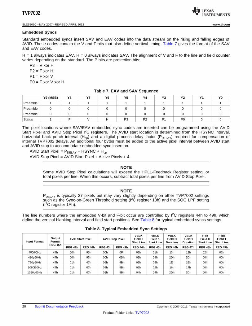
Embedded Syncs
Standard embedded syncs insert SAV and EAV codes into the data stream on the rising and falling edges ofAVID. These codes contain the V and F bits that also define vertical timing. Table 7 gives the format of the SAVand EAV codes.
H = 1 always indicates EAV. H = 0 always indicates SAV. The alignment of V and F to the line and field countervaries depending on the standard. The P bits are protection bits:
P3 = V xor HP2 = F xor HP1 = F xor VP0 = F xor V xor H
Table 7. EAV and SAV Sequence
Y9 (MSB) Y8 Y7 Y6 Y5 Y4 Y3 Y2 Y1 Y0
Preamble 1 1 1 1 1 1 1 1 1 1
Preamble 0 0 0 0 0 0 0 0 0 0
Preamble 0 0 0 0 0 0 0 0 0 0
Status 1 F V H P3 P2 P1 P0 0 0
The pixel locations where SAV/EAV embedded sync codes are inserted can be programmed using the AVIDStart Pixel and AVID Stop Pixel I2C registers. The AVID start location is determined from the HSYNC interval,horizontal back porch interval (Hbp) and a digital process delay factor (PDELAY) required for compensation ofinternal TVP7002 delays. An additional four bytes must be added to the active pixel interval between AVID startand AVID stop to accommodate embedded sync insertion.
AVID Start Pixel = PDELAY + HSYNC + Hbp
AVID Stop Pixel = AVID Start Pixel + Active Pixels + 4
NOTESome AVID Stop Pixel calculations will exceed the HPLL-Feedback Register setting, ortotal pixels per line. When this occurs, subtract total pixels per line from AVID Stop Pixel.
NOTEPDELAY is typically 27 pixels but may vary slightly depending on other TVP7002 settingssuch as the Sync-on-Green Threshold setting (I2C register 10h) and the SOG LPF setting(I2C register 1Ah).
The line numbers where the embedded V-bit and F-bit occur are controlled by I2C registers 44h to 49h, whichdefine the vertical blanking interval and field start positions. See Table 8 for typical embedded syncs settings.
Table 8. Typical Embedded Sync Settings
VBLK VBLK VBLK VBLK F-bit F-bitOutput AVID Start Pixel AVID Stop Pixel Field 0 Field 1 Field O Field 1 Field 0 Field 1
Input Format Format Start Line Start Line Duration Duration Start Line Start LineREG 15h
REG 41h REG 40h REG 43h REG 42h REG 44h REG 45h REG 46h REG 47h REG 48h REG 49h
480i60Hz 47h 00h 95h 00h 0Fh 01h 01h 13h 13h 02h 01h
480p60Hz 47h 00h 93h 00h 0Dh 09h 09h 2Dh 2Dh 00h 00h
720p60Hz 47h 01h 47h 06h 4Bh 05h 05h 1Eh 1Eh 00h 00h
1080i60Hz 47h 01h 07h 08h 8Bh 02h 02h 16h 17h 00h 00h
1080p60Hz 47h 01h 07h 08h 8Bh 04h 04h 2Dh 2Dh 00h 00h
20 Submit Documentation Feedback Copyright © 2007–2013, Texas Instruments Incorporated
Product Folder Links: TVP7002

TVP7002
www.ti.com SLES206C –MAY 2007–REVISED APRIL 2013
Output Range Limits
The TVP7002 provides selectable output range limits in I2C subaddress 15h:00 = RGB coding range (Y, Cb, and Cr range from 0 to 1023) (default)01 = Extended coding range (Y, Cb, and Cr range from 4 to 1019)10 = ITU-R BT.601 coding range (Y ranges from 64 to 940, Cb and Cr range from 64 to 960)11 = Reserved
NOTERGB coding range not allowed with embedded syncs.
Power Management
The TVP7002 supports both automatic and manual power-down modes. The automatic power-down mode canbe selected by setting bit 2 of subaddress 0Fh to logic 0.
In the automatic power-down mode, the TVP7002 powers down the ADCs, the ADC reference, and horizontalPLL when activity is not detected on both the selected HSYNC input and the selected SOG input (VSYNC is nolonger used). The TVP7002 restores power whenever activity is detected on either the selected HSYNC input orthe selected SOG input.
The TVP7002 can also be placed in power-down mode via the active-high PWDN input (pin 70). When thePWDN input is driven high, the TVP7002 powers down everything including the I2C interface, and the digitaloutputs are not placed in a high-impedance mode.
The TVP7002 can also be placed in a power-down mode using bit 1 of register 0Fh.
Individual blocks of the TVP7002 can be independently powered down using register 2Bh.
Copyright © 2007–2013, Texas Instruments Incorporated Submit Documentation Feedback 21
Product Folder Links: TVP7002

4:4:4 RGB Output Timing. RGB output latency (RGB ) is 18 clock cycles. HSOUT latency (HS ) is 5 clock cycles with HS Start set to 0.PD PD
4:2:2 YCbCr Output Timing. YCbCr output latency (YC ) is 39 clock cycles. HSOUT latency (HS ) is 5 clock cycles with HS Start set to 0.PD PD
TVP7002
SLES206C –MAY 2007–REVISED APRIL 2013 www.ti.com
Timing
The TVP7002 supports RGB/YCbCr 4:4:4 and YCbCr 4:2:2 modes. Output timing is shown in Figure 6. All timingdiagrams are shown for operation with internal PLL clock at phase 0 and HSOUT Output Start = 0. For the 4:2:2mode, CbCr data output is on the BOUT[9:0] output port.
Figure 6. Output Timing Diagram
22 Submit Documentation Feedback Copyright © 2007–2013, Texas Instruments Incorporated
Product Folder Links: TVP7002

TVP7002
www.ti.com SLES206C –MAY 2007–REVISED APRIL 2013
I2C Host Interface
Communication with the TVP7002 device is via an I2C host interface. The I2C standard consists of two signals,serial input/output data (SDA) line and input clock line (SCL), which carry information between the devicesconnected to the bus. A third signal (I2CA) is used for slave address selection. Although an I2C system can bemulti-mastered, the TVP7002 can function as a slave device only.
Since SDA and SCL are kept open drain at logic high output level or when the bus is not driven, the user shouldconnect SDA and SCL to a positive supply voltage via a pullup resistor on the board. SDA is implementedbidirectional. The slave addresses select, terminal 73 (I2CA), enables the use of two TVP7002 devices tied to thesame I2C bus, as it controls the least significant bit of the I2C device address
Table 9. I2C Host Interface Terminal Description
SIGNAL TYPE DESCRIPTION
I2CA I Slave address selection
SCL I Input clock line
SDA I/O Input/output data line
Reset and I2C Bus Address Selection
The TVP7002 can respond to two possible chip addresses. The I2 slave address is continuously interpreted fromthe logic level present at the I2CA terminal. The I2C slave address must be configured with an externalconnection to either IOGND (I2C address = B8h) or IOVDD (I2C address= BAh). A 2.2-kΩ pullup or pulldownresistor may be used for this connection.
Table 10. I2C Host Interface Device Addresses
A6 A5 A4 A3 A2 A1 A0 (I2CA) R/W HEX
1 0 1 1 1 0 0 (1) 1/0 B9h/B8h
1 0 1 1 1 0 1 (2) 1/0 BBh/BAh
(1) If I2CA terminal 73 is strapped to IOGND, I2C device address A0 is set to 0.(2) If I2CA terminal 73 is strapped to IOVDD, I2C device address A0 is set to 1.
I2C Operation
Data transfers occur utilizing the following illustrated formats.
S 10111000 ACK Subaddress ACK Send data ACK P
Read from I2C control registers
S 10111000 ACK Subaddress ACK S 10111001 ACK Receive data NAK P
S = I2C bus Start condition
P = I2C bus Stop condition
ACK = Acknowledge generated by the slave
NAK = Acknowledge generated by the master, for multiple byte read master with ACK each byte except last byte
Subaddress = Subaddress byte
Data = Data byte, if more than one byte of DATA is transmitted (read and write), the subaddress pointer isautomatically incremented
I2C bus address = Example shown that I2CA is in default mode; write (B8h), read (B9h).
Copyright © 2007–2013, Texas Instruments Incorporated Submit Documentation Feedback 23
Product Folder Links: TVP7002
Power
Reset
I C2
5 ms 1 µs
TVP7002
SLES206C –MAY 2007–REVISED APRIL 2013 www.ti.com
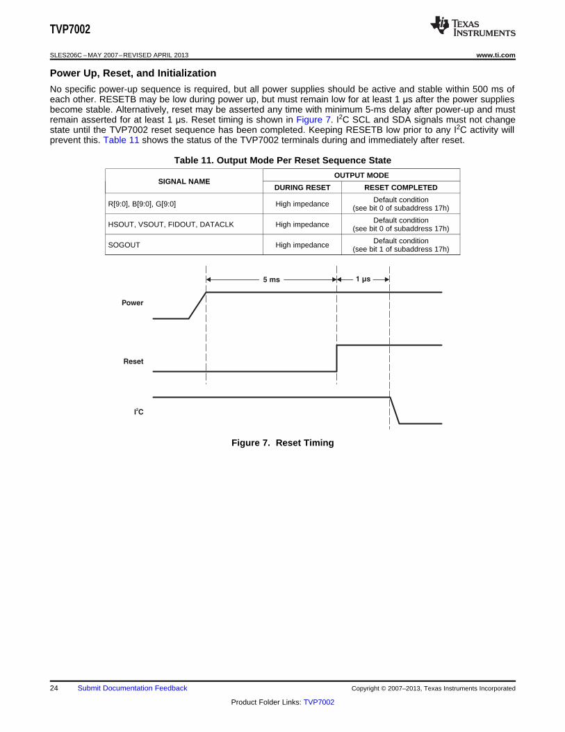
Power Up, Reset, and Initialization
No specific power-up sequence is required, but all power supplies should be active and stable within 500 ms ofeach other. RESETB may be low during power up, but must remain low for at least 1 μs after the power suppliesbecome stable. Alternatively, reset may be asserted any time with minimum 5-ms delay after power-up and mustremain asserted for at least 1 μs. Reset timing is shown in Figure 7. I2C SCL and SDA signals must not changestate until the TVP7002 reset sequence has been completed. Keeping RESETB low prior to any I2C activity willprevent this. Table 11 shows the status of the TVP7002 terminals during and immediately after reset.
Table 11. Output Mode Per Reset Sequence State
OUTPUT MODESIGNAL NAME
DURING RESET RESET COMPLETED
Default conditionR[9:0], B[9:0], G[9:0] High impedance (see bit 0 of subaddress 17h)
Default conditionHSOUT, VSOUT, FIDOUT, DATACLK High impedance (see bit 0 of subaddress 17h)
Default conditionSOGOUT High impedance (see bit 1 of subaddress 17h)
Figure 7. Reset Timing
24 Submit Documentation Feedback Copyright © 2007–2013, Texas Instruments Incorporated
Product Folder Links: TVP7002

TVP7002
www.ti.com SLES206C –MAY 2007–REVISED APRIL 2013
CONTROL REGISTERS
The TVP7002 is initialized and controlled by a set of internal registers that define the operating parameters of theentire device. Communication between the external controller and the TVP7002 is through a standard I2C hostport interface, as previously described.
Table 12 shows the summary of these registers. Detailed programming information for each register is describedin the following sections.
Table 12. Control Registers Summary (1) (2)
REGISTER NAME I2C SUBADDRESS DEFAULT R/W (3)
Chip Revision 00h 02h R
H-PLL Feedback Divider MSBs 01h 67h R/W
H-PLL Feedback Divider LSBs 02h 20h R/W
H-PLL Control 03h A8h R/W
H-PLL Phase Select 04h 80h R/W
Clamp Start 05h 32h R/W
Clamp Width 06h 20h R/W
HSYNC Output Width 07h 20h R/W
Blue Fine Gain 08h 00h R/W
Green Fine Gain 09h 00h R/W
Red Fine Gain 0Ah 00h R/W
Blue Fine Offset MSBs 0Bh 80h R/W
Green Fine Offset MSBs 0Ch 80h R/W
Red Fine Offset MSBs 0Dh 80h R/W
Sync Control 1 0Eh 5Bh R/W
H-PLL and Clamp Control 0Fh 2Eh R/W
Sync On Green Threshold 10h 5Dh R/W
Sync Separator Threshold 11h 20h R/W
H-PLL Pre-Coast 12h 00h R/W
H-PLL Post-Coast 13h 00h R/W
Sync Detect Status 14h R
Output Formatter 15h 04h R/W
MISC Control 1 16h 11h R/W
MISC Control 2 17h 03h R/W
MISC Control 3 18h 00h R/W
Input Mux Select 1 19h 00h R/W
Input Mux Select 2 1Ah C2h R/W
Blue and Green Coarse Gain 1Bh 77h R/W
Red Coarse Gain 1Ch 07h R/W
Fine Offset LSBs 1Dh 00h R/W
Blue Coarse Offset 1Eh 10h R/W
Green Coarse Offset 1Fh 10h R/W
Red Coarse Offset 20h 10h R/W
HSOUT Output Start 21h 0Dh R/W
MISC Control 4 22h 08h R/W
Blue Digital ALC Output LSBs 23h R
Green Digital ALC Output LSBs 24h R
(1) For proper operation of the TVP7002 device, the default settings for all register locations designated as "Reserved" in the register mapsummary should never be changed from the values provided.
(2) For registers with reserved bits, a 0b must be written to reserved bit locations, unless otherwise stated.(3) R = Read only, W = Write only, R/W = Read/Write
Copyright © 2007–2013, Texas Instruments Incorporated Submit Documentation Feedback 25
Product Folder Links: TVP7002

TVP7002
SLES206C –MAY 2007–REVISED APRIL 2013 www.ti.com
Table 12. Control Registers Summary(1) (2) (continued)
REGISTER NAME I2C SUBADDRESS DEFAULT R/W (3)
Red Digital ALC Output LSBs 25h R
Automatic Level Control Enable 26h 80h R/W
Digital ALC Output MSBs 27h R
Automatic Level Control Filter 28h 53h R/W
Reserved 29h 08h R/W
Fine Clamp Control 2Ah 07h R/W
Power Control 2Bh 00h R/W
ADC Setup 2Ch 50h R/W
Coarse Clamp Control 2Dh 00h R/W
SOG Clamp 2Eh 80h R/W
RGB Coarse Clamp Control 2Fh 8Ch R/W
SOG Coarse Clamp Control 30h 04h R/W
ALC Placement 31h 5Ah R/W
Reserved 32h 18h R/W
Reserved 33h 60h R/W
Macrovision Stripper Width 34h 03h R/W
VSYNC Alignment 35h 10h R/W
Sync Bypass 36h 00h R/W
Lines Per Frame Status 37h–38h R
Clocks Per Line Status 39h–3Ah R
HSYNC Width 3Bh R
VSYNC Width 3Ch R
Line Length Tolerance 3Dh 03h R/W
Reserved 3Eh 04h R/W
Video Bandwidth Control 3Fh 00h R/W
AVID Start Pixel 40h–41h 012Ch R/W
AVID Stop Pixel 42h–43h 062Ch R/W
VBLK Field 0 Start Line Offset 44h 05h R/W
VBLK Field 1 Start Line Offset 45h 05h R/W
VBLK Field 0 Duration 46h 1Eh R/W
VBLK Field 1 Duration 47h 1Eh R/W
F-bit Field 0 Start Line Offset 48h 00h R/W
F-bit Field 1 Start Line Offset 49h 00h R/W
1st CSC Coefficient 4Ah–4Bh 16E3h R/W
2nd CSC Coefficient 4Ch–4Dh 024Fh R/W
3rd CSC Coefficient 4Eh–4Fh 06CEh R/W
4th CSC Coefficient 50h–51h F3ABh R/W
5th CSC Coefficient 52h–53h 1000h R/W
6th CSC Coefficient 54h–55h FC55h R/W
7th CSC Coefficient 56h–57h F178h R/W
8th CSC Coefficient 58h–59h FE88h R/W
9th CSC Coefficient 5Ah–5Bh 1000h R/W
Reserved 5Ch–5Dh 0000h R/W
Reserved 5Eh–FFh 0000h R/W
26 Submit Documentation Feedback Copyright © 2007–2013, Texas Instruments Incorporated
Product Folder Links: TVP7002

TVP7002
www.ti.com SLES206C –MAY 2007–REVISED APRIL 2013
Register Definitions
Chip Revision
Subaddress 00h Read Only
7 6 5 4 3 2 1 0
Chip revision [7:0]
Chip revision [7:0]: Chip revision number
H-PLL Feedback Divider MSBs
Subaddress 01h Default (67h)
7 6 5 4 3 2 1 0
PLL divide [11:4]
PLL divide [11:0]: Controls the 12-bit horizontal PLL feedback divider value that determines the number of pixels per line. PLL divide [11:4]bits should be loaded first whenever a change is required.
H-PLL Feedback Divider LSBs
Subaddress 02h Default (20h)
7 6 5 4 3 2 1 0
PLL divide [3:0] Reserved
PLL divide [11:0]: Controls the 12-bit horizontal PLL feedback divider value that determines the number of pixels per line. PLL divide [11:4]bits should be loaded first whenever a change is required.
H-PLL Control
Subaddress 03h Default (A8h)
7 6 5 4 3 2 1 0
VCO [1:0] Charge Pump Current [2:0] Reserved
VCO [1:0]: Selects VCO frequency range
VCO Gain VCO Range Pixel Clock Frequency (PCLK)(KVCO)
00 = 75 Ultra low PCLK < 36 MHz
01 = 85 Low 36 MHz ≤ PCLK < 70 MHz
10 = 150 Medium (default) 70 MHz ≤ PCLK < 135 MHz
11 = 200 High 135 MHz ≤ PCLK ≤ 165 MHz
Charge Pump Current [2:0]: Selects PLL charge pump current setting. The recommended charge pump current setting (ICP) can bedetermined using the following equation.
ICP = 40 × KVCO/(pixels per line)
000 = 0: Small
101 = 5 (default)
111 = 7: Large
NOTE: Also see the PLL and CLAMP Control register at subaddress 0Fh.
Copyright © 2007–2013, Texas Instruments Incorporated Submit Documentation Feedback 27
Product Folder Links: TVP7002

TVP7002
SLES206C –MAY 2007–REVISED APRIL 2013 www.ti.com
H-PLL Phase Select
Subaddress 04h Default (80h)
7 6 5 4 3 2 1 0
Phase Select [4:0] Reserved DIV2
Phase Select [4:0]: ADC sampling clock phase select. (1 LSB = 360/32 = 11.25°). A host-based automatic phase control algorithm can beused to control this setting to optimize graphics sampling phase.
00h = 0 degrees
10h = 180 degrees (default)
1Fh = 348.75 degrees
DIV2: DATACLK divide-by-2. H-PLL post divider. May be used with a 2x H-PLL feedback divider to improve jitter at low frequencies. Whenused, only half of the Phase Select [4:0] settings are functional.
0 = DATACLK/1 (default)
1 = DATACLK/2
Clamp Start
Subaddress 05h Default (32h)
7 6 5 4 3 2 1 0
Clamp Start [7:0]
Clamp Start [7:0]: Positions the clamp signal an integer number of clock periods after the HSYNC signal. If external clamping is selectedthis value has no meaning. Clamp Start must be correctly positioned for proper operation. See Table 13 for the recommended settings.
Clamp Width
Subaddress 06h Default (20h)
7 6 5 4 3 2 1 0
Clamp Width [7:0]
Clamp Width [7:0]: Sets the width in pixels for the fine clamp. See also register Clamp Start (subaddress 05h).
Table 13. Recommended Fine Clamp Settings
VIDEO STANDARD CLAMP START CLAMP WIDTH
HDTV (tri-level) 50 (32h) 32 (20h)
SDTV (bi-level) 6 (06h) 16 (10h)
PC graphics 6 (06h) 16 (10h)
HSYNC Output Width
Subaddress 07h Default (20h)
7 6 5 4 3 2 1 0
HSOUT Width [7:0]
HSOUT Width [7:0]: Sets the width in pixels for HSYNC output.
Blue Fine Gain
Subaddress 08h Default (00h)
7 6 5 4 3 2 1 0
Blue Fine Gain [7:0]
Blue Fine Gain [7:0]: 8-bit fine digital gain (contrast) for Blue channel (applied after the ADC). Offset binary value.
Blue Fine Gain = 1 + Blue Fine Gain [7:0]/256
Blue Fine Gain [7:0] Blue Fine Gain
00h 1.0 (default)
80h 1.5
FFh 2.0
28 Submit Documentation Feedback Copyright © 2007–2013, Texas Instruments Incorporated
Product Folder Links: TVP7002

TVP7002
www.ti.com SLES206C –MAY 2007–REVISED APRIL 2013
Green Fine Gain
Subaddress 09h Default (00h)
7 6 5 4 3 2 1 0
Green Fine Gain [7:0]
Green Fine Gain [7:0]: 8-bit fine digital gain (contrast) for Green channel (applied after the ADC). Offset binary value.
Green Fine Gain = 1 + Green Fine Gain [7:0]/256
Green Fine Gain [7:0] Green Fine Gain
00h 1.0 (default)
80h 1.5
FFh 2.0
Red Fine Gain
Subaddress 0Ah Default (00h)
7 6 5 4 3 2 1 0
Red Fine Gain [7:0]
Red Fine Gain [7:0]: 8-bit fine digital gain (contrast) for Red channel (applied after the ADC). Offset binary value.
Red Fine Gain = 1 + Red Fine Gain [7:0]/256
Red Fine Gain [7:0] Red Fine Gain
00h 1.0 (default)
80h 1.5
FFh 2.0
Blue Fine Offset MSBs
Subaddress 0Bh Default (80h)
7 6 5 4 3 2 1 0
Blue Fine Offset [9:2]
Blue Fine Offset [9:2]: Eight MSBs of 10-bit fine digital offset (brightness) for Blue channel (applied after ADC). Corresponding two LSBslocated at register 1Dh. Offset binary value.
The default setting of 80h places the bottom-level (RGB) clamped output blank levels at 0 and mid-level clamped (PbPr) output blank levelsat 512.
FFh = Maximum fine offset
81h = 1 LSB
80h = 0 (default)
7Fh = –1 LSB
00h = Minimum fine offset
Green Fine Offset MSBs
Subaddress 0Ch Default (80h)
7 6 5 4 3 2 1 0
Green Fine Offset [9:2]
Green Fine Offset [9:2]: Eight MSBs of 10-bit fine digital offset (brightness) for Green channel (applied after ADC). Corresponding two LSBslocated at register 1Dh. Offset binary value.
The default setting of 80h places the bottom-level (RGB) clamped output blank levels at 0 and mid-level clamped (PbPr) output blank levelsat 512.
FFh = Maximum fine offset
81h = 1 LSB
80h = 0 (default)
7Fh = –1 LSB
00h = Minimum fine offset
Copyright © 2007–2013, Texas Instruments Incorporated Submit Documentation Feedback 29
Product Folder Links: TVP7002

TVP7002
SLES206C –MAY 2007–REVISED APRIL 2013 www.ti.com
Red Fine Offset MSBs
Subaddress 0Dh Default (80h)
7 6 5 4 3 2 1 0
Red Fine Offset [9:2]
Red Fine Offset [9:2]: 8 MSBs of 10-bit fine digital offset (brightness) for Red channel (applied after ADC). Corresponding two LSBs locatedat register 1Dh. Offset binary value.
The default setting of 80h places the bottom-level (RGB) clamped output blank levels at 0 and mid-level clamped (PbPr) output blank levelsat 512.
FFh = Maximum fine offset
81h = 1 LSB
80h = 0 (default)
7Fh = –1 LSB
00h = Minimum fine offset
Sync Control 1
Subaddress 0Eh Default (5Bh)
7 6 5 4 3 2 1 0
HSPO HSIP HSOP AHSO AHSS VSOP AVSO AVSS
HSPO: HSYNC polarity override
0 = Polarity determined by chip (default)
1 = Polarity set by bit 6 in register 0Eh (not recommended)
HSIP: HSYNC input polarity
0 = Indicates input HSYNC polarity active low
1 = Indicates input HSYNC polarity active high (default)
HSOP: HSYNC output polarity
0 = Active-low HSYNC output (default)
1 = Active-high HSYNC output
NOTE: HSOP has no effect in raw sync bypass mode. See register 36h.
AHSO: Active HSYNC override
0 = Active HSYNC is automatically selected by TVP7002. If selected, SOG and HSYNC inputs both have active inputs,HSYNC is selected as the active sync source. The selected active HSYNC is provided via the AHS status bit (bit 6 ofregister 14h).
1 = Active HSYNC is manually selected via the AHSS control bit (bit 3 of register 0Eh). (default)
NOTE: Automatic sync selection should be enabled only for 5-wire PC graphics inputs.
AHSS: Active HSYNC select. The indicated HSYNC is used only if the AHSO control bit (bit 4) is set to 1 or if activity is detected on boththe selected HSYNC input and the selected SOG input (bits 1, 7 = 1 in register 14h).
0 = Active HSYNC is derived from the selected HSYNC input.
1 = Active HSYNC is derived from the selected SOG input (default).
VSOP: VSYNC output polarity
0 = Active-low VSYNC output (default)
1 = Active-high VSYNC output
AVSO: Active VSYNC override
0 = Active VSYNC is automatically selected by TVP7002. If selected, SOG and VSYNC inputs both have active inputs,VSYNC is selected as the active sync source. The selected active VSYNC is provided via the AVS status bit (bit 3 ofregister 14h).
1 = Active VSYNC is manually selected via the AVSS control bit (bit 0 of register 0Eh) (default).
NOTE: Automatic sync selection should be enabled only for 5-wire PC graphics inputs.
AVSS: Active VSYNC select. This bit is effective when the AVSO control bit (bit 1) is set to 1.
0 = Active VSYNC is derived from the selected VSYNC input.
1 = Active VSYNC is derived from the Sync separated VSYNC (default).
30 Submit Documentation Feedback Copyright © 2007–2013, Texas Instruments Incorporated
Product Folder Links: TVP7002

TVP7002
www.ti.com SLES206C –MAY 2007–REVISED APRIL 2013
H-PLL and Clamp Control
Subaddress 0Fh Default (2Eh)
7 6 5 4 3 2 1 0
CF CP Coast Sel CPO CPC SMO FCPD ADC Test
CF: Clamp Function. Clamp pulse select. This control bit determines whether the timing for both the fine clamp and the ALC circuit aregenerated internally or externally.
0 = Internal fine clamp and ALC timing (default)
1 = External fine clamp and ALC timing (pin 76)
CP: Clamp Polarity. External clamp polarity select
0 = Active-high clamp pulse (default)
1 = Active-low clamp pulse
CS: Coast Select. Coast signal select. This control bit determines whether the timing for H-PLL coast signal is generated internally orexternally.
0 = External H-PLL coast timing (pin 77)
1 = Internal H-PLL coast timing (default)
CPO: Coast Polarity Override
0 = Polarity determined by chip (default)
1 = Polarity set be Bit 3 in register 0Fh
CPC: Coast Polarity Change. External coast polarity select
0 = Active-low coast signal
1 = Active-high coast signal (default)
SMO: Seek Mode Override. Places the TVP7002 in a low power mode whenever no activity is detected on the selected sync inputs.
0 = Enable automatic power management mode
1 = Disable automatic power management mode (default)
NOTE: Digital outputs are not high impedance and may be in a random state during low power mode. Outputs can be putin high impedance state by I2C register 17h.
FCPD: Full Chip Power Down. Active-low power down. FCPD powers down all blocks except I2C. The I2C register values are retained.
0 = Power-down mode
1 = Normal operation (default)
NOTE: Digital outputs are not high impedance and may be in random state during FCPD. Outputs can be put in highimpedance state by I2C register 17h.
ADC Test: Active-high ADC test mode select. When placed in the ADC test mode, the TVP7002 disables the fine clamp, enables thecoarse clamp, and selects the external clock input (pin 80) for each ADC channel.
0 = ADC test mode disabled (default)
1 = ADC test mode enabled
NOTE: Also see the Horizontal PLL Control register at subaddress 03h.
Copyright © 2007–2013, Texas Instruments Incorporated Submit Documentation Feedback 31
Product Folder Links: TVP7002

TVP7002
SLES206C –MAY 2007–REVISED APRIL 2013 www.ti.com
Sync-On-Green Threshold
Subaddress 10h Default (5Dh)
7 6 5 4 3 2 1 0
SOG Threshold [4:0] Blue CS Green CS Red CS
SOG Threshold [4:0]: Sets the voltage level of the SOG slicer comparator according to the following equation.
slice_level = (350 mV) × (NTH/31)
00h = 0 mV
0Bh = 124 mV (default)
1Fh = 350 mV
Blue Clamp Select: This bit has no effect when the Blue channel fine clamp is disabled (bit 2 of subaddress 2Ah).
0 = Bottom-level fine clamp
1 = Mid-level fine clamp (default)
Green Clamp Select: This bit has no effect when the Green channel fine clamp is disabled (bit 1 of subaddress 2Ah).
0 = Bottom-level fine clamp (default)
1 = Mid level fine clamp
Red Clamp Select: This bit has no effect when the Red channel fine clamp is disabled (bit 0 of subaddress 2Ah).
0 = Bottom-level fine clamp
1 = Mid-level fine clamp (default)
NOTE: Bottom-level clamping is required for Y and RGB inputs, while mid-level clamping is required for Pb and Pr inputs. The internalclamp pulse must also be correctly positioned for proper clamp operation (see register 05h)
Sync Separator Threshold
Subaddress 11h Default (20h)
7 6 5 4 3 2 1 0
Sync Separator Threshold [7:0]
Sync Separator Threshold [7:0]: Sets how many internal clock reference periods the sync separator counts to before toggling high or low.Sync Separator Threshold [7:0] × (minimum clock period) must be greater than the width of the negative sync pulse. This setting can alsoaffect the position of the VSOUT (see register 22h).
NOTE: The internal clock reference is typically 6.5 MHz, but a minimum clock period of 133 ns is recommended to allow for clock variation.
40h = recommended setting for support of most video formats
NOTE: Margin for a particular format can be maximized by using a mid-range setting below.
Format MIN MID MAX
480i60Hz 1Fh 75h ABh
480p60Hz 10h 64h BAh
576i50Hz 20h 75h ACh
576p50Hz 11h 64h BCh
720p60Hz 1Bh 43h 6Ch
720p50Hz 37h 50h 6Ch
1080i60Hz 0Eh 2Ch 4Bh
1080i50Hz 21h 36h 4Bh
1080p60Hz 08h 2Dh 53h
1080p50Hz 1Bh 36h 53h
H-PLL Pre-Coast
Subaddress 12h Default (00h)
7 6 5 4 3 2 1 0
Pre-Coast [7:0]
Pre-Coast [7:0]: Sets the number of HSYNC periods that coast becomes active prior to VSYNC leading edge. A minimum setting of 1 isrequired to guarantee generation of an internal coast signal.
32 Submit Documentation Feedback Copyright © 2007–2013, Texas Instruments Incorporated
Product Folder Links: TVP7002
TVP7002
www.ti.com SLES206C –MAY 2007–REVISED APRIL 2013
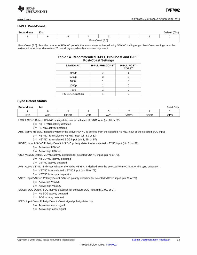
H-PLL Post-Coast
Subaddress 13h Default (00h)
7 6 5 4 3 2 1 0
Post-Coast [7:0]
Post-Coast [7:0]: Sets the number of HSYNC periods that coast stays active following VSYNC trailing edge. Post-Coast settings must beextended to include Macrovision™ pseudo syncs when Macrovision is present.
Table 14. Recommended H-PLL Pre-Coast and H-PLLPost-Coast Settings
STANDARD H-PLL PRE-COAST H-PLL POST-COAST
480i/p 3 3
576i/p 3 3
1080i 1 0
1080p 1 0
720p 1 0
PC SOG Graphics 1 0
Sync Detect Status
Subaddress 14h Read Only
7 6 5 4 3 2 1 0
HSD AHS IHSPD VSD AVS VSPD SOGD ICPD
HSD: HSYNC Detect. HSYNC activity detection for selected HSYNC input (pin 81 or 82).
0 = No HSYNC activity detected
1 = HSYNC activity detected
AHS: Active HSYNC. Indicates whether the active HSYNC is derived from the selected HSYNC input or the selected SOG input.
0 = HSYNC from selected HSYNC input (pin 81 or 82)
1 = HSYNC from selected SOG input (pin 1, 99, or 97)
IHSPD: Input HSYNC Polarity Detect. HSYNC polarity detection for selected HSYNC input (pin 81 or 82).
0 = Active-low HSYNC
1 = Active-high HSYNC
VSD: VSYNC Detect. VSYNC activity detection for selected VSYNC input (pin 78 or 79).
0 = No VSYNC activity detected
1 = VSYNC activity detected
AVS: Active VSYNC. Indicates whether the active VSYNC is derived from the selected VSYNC input or the sync separator.
0 = VSYNC from selected VSYNC input (pin 78 or 79)
1 = VSYNC from sync separator
VSPD: Input VSYNC Polarity Detect. VSYNC polarity detection for selected VSYNC input (pin 78 or 79).
0 = Active-low VSYNC
1 = Active-high VSYNC
SOGD: SOG Detect. SOG activity detection for selected SOG input (pin 1, 99, or 97).
0 = No SOG activity detected
1 = SOG activity detected
ICPD: Input Coast Polarity Detect. Coast signal polarity detection.
0 = Active-low coast signal
1 = Active-high coast signal
Copyright © 2007–2013, Texas Instruments Incorporated Submit Documentation Feedback 33
Product Folder Links: TVP7002

TVP7002
SLES206C –MAY 2007–REVISED APRIL 2013 www.ti.com
Output Formatter
Subaddress 15h Default (04h)
7 6 5 4 3 2 1 0
Reserved Output code range [1:0] Reserved Clamp REF CbCr order 422/444 Sync En
Reserved [7]:
0 = Required (default)
Output code range [1:0]:
00 = RGB coding range (Y, Cb, and Cr range from 0 to 1023) (default)
01 = Extended coding range (Y, Cb, and Cr range from 4 to 1019)
10 = ITU-R BT.601 coding range (Y ranges from 64 to 940, Cb and Cr range from 64 to 960)
11 = Reserved
Reserved [4]:
0 = Required (default)
Clamp REF: Selects which edge of HSYNC is used as the timing reference for the fine clamp pulse placement and also the ALCplacement.
0 = Clamp pulse placement referred to the trailing edge of HSYNC (default)
1 = Clamp pulse placement referred to the leading edge of HSYNC
CbCr order: This bit is only effective in the 4:2:2 output mode (i.e., bit 1 is set to 1).
0 = CbCr order
1 = CrCb order (default)
422/444: Active-high 4:4:4 to 4:2:2 decimation filter enable
0 = 30-bit 4:4:4 output format (default)
1 = 20-bit 4:2:2 output format
Notes:1. Multiplexed CbCr data is output on BOUT [9:0] in the 20-bit 4:2:2 output format.2. 10-bit 4:2:2 output format is not supported.
Sync En: Active-high embedded sync enable
0 = Embedded sync disabled (default)
1 = Embedded sync enabled
Notes:1. Embedded syncs are not supported when the RGB coding range (0 to 1023) is selected.2. Embedded syncs are not supported when the 30-bit 4:4:4 output format is selected.3. Discrete syncs are always enabled except when outputs are placed in the high-impedance mode.4. When enabled, embedded syncs are present in both the Y and C outputs.
MISC Control 1
Subaddress 16h Default (11h)
7 6 5 4 3 2 1 0
Reserved CbCr Align Reserved PLL PD STRTB
CbCr Align: CbCr alignment
0 = Alternative operation
1 = Normal operation (default)
PLL PD: Active-high H-PLL power down
0 = Normal operation (default)
1 = H-PLL powered down
STRTB: Active-high H-PLL start-up circuit enable
0 = H-PLL start-up circuit disabled
1 = H-PLL start-up circuit enabled (default)
34 Submit Documentation Feedback Copyright © 2007–2013, Texas Instruments Incorporated
Product Folder Links: TVP7002

TVP7002
www.ti.com SLES206C –MAY 2007–REVISED APRIL 2013
MISC Control 2
Subaddress 17h Default (03h)
7 6 5 4 3 2 1 0
Reserved Test output control [2:0] Reserved SOG En Output En
Test output control [2:0]: Selects which signal is output on pin 22. Output polarity control is also provided using bit 2 of subaddress 18h.
000 = Field ID output (default)
001 = Data Enable output
010 = Reserved
011 = Reserved
100 = Internal clock reference output (~6.5 MHz typical)
101 = Coast output
110 = Clamp pulse output
111 = High-impedance mode
SOG En: Active-low output enable for SOGOUT output.
0 = SOG output enabled
1 = SOG output placed in high-impedance mode (default)
Output En: Active-low output enable for RGB, DATACLK, HSOUT, VSOUT, and FIDOUT outputs. This control bit allows selecting a high-impedance output mode for multiplexing the output of the TVP7002 with another device.
0 = Outputs enabled
1 = Outputs placed in high-impedance mode (default)
NOTE: Data Enable output is equivalent to the internal active video signal that is controlled by the AVID start/stop pixelvalues and the VBLK offset/duration line values.
MISC Control 3
Subaddress 18h Default (00h)
7 6 5 4 3 2 1 0
Reserved Reserved Blank En CSC En Reserved FID POL SOG POL CLK POL
Reserved [7]:
0 = Required (default)
Blank En: Active-high blank level enable. Forces the video blank level to a standard value when using embedded syncs.
0 = Normal operation (default)
1 = Force standard blank levels
CSC En: Active-high CSC enable. When disabled, the CSC block is bypassed.
0 = CSC disabled (default)
1 = CSC enabled
FID POL: Active-high Field ID output polarity control. Under normal operation, the field ID output is set to logic 1 for an odd field (field 1)and set to logic 0 for an even field (field 0).
0 = Normal operation (default)
1 = FID output polarity inverted
NOTE: This control bit also affects the polarity of the data enable output when selected (see Test output control [2:0] atsubaddress 17h).
SOG POL: Active-high SOG output polarity control
0 = Normal operation (default)
1 = SOG output polarity inverted
CLK POL: Allows selecting the polarity of the output data clock.
0 = Data is clocked out on rising edge of DATACLK (default)
1 = Data is clocked out on falling edge of DATACLK
Copyright © 2007–2013, Texas Instruments Incorporated Submit Documentation Feedback 35
Product Folder Links: TVP7002

TVP7002
SLES206C –MAY 2007–REVISED APRIL 2013 www.ti.com
Input Mux Select 1
Subaddress 19h Default (00h)
7 6 5 4 3 2 1 0
SOG Select [1:0] Red Select [1:0] Green Select [1:0] Blue Select [1:0]
SOG Select [1:0]: Selects one of three SOG inputs.
00 = SOGIN_1 input selected (default)
01 = SOGIN_2 input selected
10 = SOGIN_3 input selected
11 = Reserved
Red Select [1:0]: Selects one of three R/Pr inputs.
00 = RIN_1 input selected (default)
01 = RIN_2 input selected
10 = RIN_3 input selected
11 = Reserved
Green Select [1:0]: Selects one of four G/Y inputs.
00 = GIN_1 input selected (default)
01 = GIN_2 input selected
10 = GIN_3 input selected
11 = GIN_4 input selected
Blue Select [1:0]: Selects one of three B/Pb inputs.
00 = BIN_1 input selected (default)
01 = BIN_2 input selected
10 = BIN_3 input selected
11 = Reserved
36 Submit Documentation Feedback Copyright © 2007–2013, Texas Instruments Incorporated
Product Folder Links: TVP7002

TVP7002
www.ti.com SLES206C –MAY 2007–REVISED APRIL 2013
Input Mux Select 2
Subaddress 1Ah Default (C2h)
7 6 5 4 3 2 1 0
SOG LPF SEL [1:0] CLP LPF SEL [1:0] CLK SEL VS SEL PCLK SEL HS SEL
SOG LPF SEL [1:0]: SOG low-pass filter selection. The SOG low-pass filter can be used to attenuate glitches present onthe SOG input. Excessive filtering can lead to sync detection issues and increased sample clock jitter.
00 = 2.5-MHz low-pass filter
01 = 10-MHz low-pass filter
10 = 33-MHz low-pass filter
11 = Low-pass filter bypass (default)
CLP LPF SEL [1:0]: Coarse clamp low-pass filter selection. This filter effects the operation of all enabled coarse clamps which is generallythe SOG coarse clamp only.
00 = 4.8-MHz low-pass filter (default). Suitable for HDTV and graphics formats.
01 = 0.5-MHz low-pass filter. Suitable for SDTV formats.
10 = 1.7-MHz low-pass filter
11 = Reserved
CLK SEL: Clock reference select for Sync Processing block. The internal reference clock is typically 6.5 MHz, but it should not beconsidered a precise clock. An external 27-MHz reference clock is therefore recommended for accurate mode detection. NOTE: The I2Cinterface, Sync Separator, and activity detection circuitry always uses the internal clock reference.
0 = Internal clock reference (default)
1 = External clock reference (EXT_CLK)
NOTE: The external clock input can also be selected as the sample clock for the ADCs (see bit 1).
VS SEL: VSYNC input select
0 = VSYNC_A input selected (default)
1 = VSYNC_B input selected
PCLK SEL: Pixel clock selection. When the external clock input (pin 80) is selected as the ADC sample clock, the external clamp pulse(pin 76) should also be selected (Bit 7 of subaddress 0Fh).
0 = ADC samples data using external clock input (pin 80)
1 = ADC samples data using H-PLL generated clock (default)
NOTE: The external clock input can also be selected as the reference clock for the Sync Processing block (see bit 3).
HS SEL: HSYNC input select
0 = HSYNC_A input selected (default)
1 = HSYNC_B input selected
NOTE: See the Sync Control register at subaddress 0Eh.
Copyright © 2007–2013, Texas Instruments Incorporated Submit Documentation Feedback 37
Product Folder Links: TVP7002

TVP7002
SLES206C –MAY 2007–REVISED APRIL 2013 www.ti.com
Blue and Green Coarse Gain
Subaddress 1Bh Default (77h)
7 6 5 4 3 2 1 0
Green Coarse Gain [3:0] Blue Coarse Gain [3:0]
Green Coarse Gain [3:0]: 4-bit coarse analog gain for Green channel (applied before the ADC). To avoid clipping at the ADC, VP-P in XGain must be less than 1 VP-P.
Gain [3:0] Description
0000 = 0.5
0001 = 0.6
0010 = 0.7
0011 = 0.8
0100 = 0.9
0101 = 1.0
0110 = 1.1
0111 = 1.2 Default
1000 = 1.3 Maximum recommended gain for 700 mVP-P input
1001 = 1.4
1010 = 1.5
1011 = 1.6
1100 = 1.7
1101 = 1.8
1110 = 1.9
1111 = 2.0
Blue Coarse Gain [3:0]: 4-bit coarse analog gain for Blue channel (applied before the ADC).
Red Coarse Gain
Subaddress 1Ch Default (07h)
7 6 5 4 3 2 1 0
Reserved Red Coarse Gain [3:0]
Red Coarse Gain [3:0]: 4-bit coarse analog gain for Red channel (applied before ADC).
Fine Offset LSBs
Subaddress 1Dh Default (00h)
7 6 5 4 3 2 1 0
Reserved Red Fine Offset [1:0] Green Fine Offset [1:0] Blue Fine Offset [1:0]
Red Fine Offset [1:0]: Two LSBs of 10-bit fine digital offset for Red channel (applied after ADC). Corresponding eight MSBs located atregister 0Dh. Offset binary value
Green Fine Offset [1:0]: Two LSBs of 10-bit fine digital offset for Green channel (applied after ADC). Corresponding eight MSBs located atregister 0Ch. Offset binary value.
Blue Fine Offset [1:0]: Two LSBs of 10-bit fine digital offset for Blue channel (applied after ADC). Corresponding eight MSBs located atregister 0Bh. Offset binary value.
38 Submit Documentation Feedback Copyright © 2007–2013, Texas Instruments Incorporated
Product Folder Links: TVP7002

TVP7002
www.ti.com SLES206C –MAY 2007–REVISED APRIL 2013
Blue Coarse Offset
Subaddress 1Eh Default (10h)
7 6 5 4 3 2 1 0
Reserved Blue Coarse Offset [5:0]
Blue Coarse Offset [5:0]: 6-bit coarse analog offset for Blue channel (applied before ADC). 6-bit sign magnitude value. Coarse Offsetsettings less than 10h can lead to bottom level clipping at the ADC input.
1Fh = +124 counts
10h = +64 counts referred to ADC output (default)
01h = +4 counts
00h = +0 counts
20h = –0 counts
21h = –4 counts
3Fh = –124 LSB
Green Coarse Offset
Subaddress 1Fh Default (10h)
7 6 5 4 3 2 1 0
Reserved Green Coarse Offset [5:0]
Green Coarse Offset [5:0]: 6-bit coarse analog offset for Green channel (applied before ADC). 6-bit sign magnitude value.
Red Coarse Offset
Subaddress 20h Default (10h)
7 6 5 4 3 2 1 0
Reserved Red Coarse Offset [5:0]
Red Coarse Offset [5:0]: 6-bit coarse analog offset for Red channel (applied before ADC). 6-bit sign magnitude value.
HSOUT Output Start
Subaddress 21h Default (0Dh)
7 6 5 4 3 2 1 0
HSOUT Start [7:0]
HSOUT Start [7:0]: Adjusts the leading edge of the HSYNC output relative to the leading edge of the HSYNC input in pixel or clock cycles.
Copyright © 2007–2013, Texas Instruments Incorporated Submit Documentation Feedback 39
Product Folder Links: TVP7002

TVP7002
SLES206C –MAY 2007–REVISED APRIL 2013 www.ti.com
MISC Control 4
Subaddress 22h Default (08h)
7 6 5 4 3 2 1 0
SP Reset Yadj_delay [2:0] MAC_EN Coast Dis VS Select VS Bypass
SP Reset: Active-high reset for Sync Processing block. This bit may be used to manually reset the sync separator, sync accumulator,activity and polarity detectors, and line and pixels counters.
0 = Normal operation (default)
1 = Sync processing reset
Yadj_delay [2:0]: Adjusts the phase delay of the luma output relative to the chroma output. Used to compensate for the chroma delayassociated with the 4:4:4 to 4:2:2 chroma sample conversion.
0h = Minimum delay (default)
7h = Maximum delay
MAC_EN: Toggling of the MAC_EN bit was required for TVP7000 and TVP7001 Macrovision support. This is no longer required with theTVP7002.
0 = Macrovision stripper disabled (recommended setting for nominal HD and PC graphics inputs).
1 = Macrovision stripper enabled (default)
NOTE: When the Macrovsion stripper is enabled, ALC and Clamp pulse placement is affected by the Macrovision StripperWidth setting. See Register 34h for details.
Coast Dis: Active-high internal coast signal disable for 5-wire PC graphics inputs. Has no effect when the external coast signal is selected.See bit 5 of register 0Fh.
0 = Internal coast signal enabled (default)
1 = Internal coast signal disabled
VS Select: VSYNC select
0 = VSOUT is generated by the sync separator (default). When there is no sync separator activity, VSOUTwill be generated by the half line accumulator .
1 = VSOUT is generated by the half line accumulator
VS Bypass: VSYNC timing bypass
0 = Normal operation (default). VS is derived from the sync separator or half line accumulator based on VS select, and theinternal pixel/line counters. Register 35h can be used to adjust VSOUT alignment relative to HSOUT.
1 = Bypass VSYNC processing. VSOUT is derived directly from the sync separator. VSOUT delay varies with sync separatorthreshold (register 11h). Register 35h has no effect.
Blue Digital ALC Output LSBs
Subaddress 23h Read only
7 6 5 4 3 2 1 0
Blue ALC Out [7:0]
Blue ALC Out [7:0]: Eight LSBs of 10-bit filtered digital ALC output for Blue channel. The corresponding two MSBs are located atsubaddress 27h. With the internal ALC loop enabled, the ADC dynamic range can be maximized by adjusting the coarse offset settingsbased on the ALC read back values. See registers 1Eh–20h for analog coarse offset control. If large adjustments are made to the analogcoarse offset control, adequate time must be allowed for the ALC to converge prior to reading of this register. ALC delay requirements willdepend on the ALC NSV filter settings and the video input line rate. A delay of 30ms should be adequate for a 480i input with an NSVsetting of 1/64. ALC NSV filtering can be increased following final coarse offset adjsutment. See register 28h for more information on ALCfilter settings. Twos-complement value.
ALC Out[9:0] = ADC output – 512
For bottom-level clamped inputs (YRGB):
• Target ADC output blank level = 32 to avoid bottom level clipping at ADCALC Out[9:0] = 32 – 512 = –480 = 220h
• Starting from positive offset, decrement YRGB coarse offset until ALC Out [9:0] ≤ 220hFor mid-level clamped inputs (PbPr):
• Target ADC output blank level = 512ALC Out[9:0] = 512 – 512 = 0
• Starting from positive offset, decrement PbPr coarse offset until ALC Out [9:0] ≤ 0.
40 Submit Documentation Feedback Copyright © 2007–2013, Texas Instruments Incorporated
Product Folder Links: TVP7002

TVP7002
www.ti.com SLES206C –MAY 2007–REVISED APRIL 2013
Green Digital ALC Output LSBs
Subaddress 24h Read only
7 6 5 4 3 2 1 0
Green ALC Out [7:0]
Green ALC Out [7:0]: Eight LSBs of 10-bit filtered digital ALC output for Green channel. The corresponding two MSBs are located atsubaddress 27h. Twos-complement value. Also see register 23h.
Red Digital ALC Output LSBs
Subaddress 25h Read only
7 6 5 4 3 2 1 0
Red ALC Out [7:0]
Red ALC Out [7:0]: Eight LSBs of 10-bit filtered digital ALC output for Red channel. The corresponding two MSBs are located atsubaddress 27h. Twos-complement value. Also see register 23h.
Automatic Level Control Enable
Subaddress 26h Default (80h)
7 6 5 4 3 2 1 0
ALC enable Reserved
ALC enable: Active-high automatic level control (ALC) enable
0 = ALC disabled
1 = ALC enabled (default)
See the ALC Placement register located at subaddress 31h.
Digital ALC Output MSBs
Subaddress 27h Read only
7 6 5 4 3 2 1 0
Reserved Red ALC Out [9:8] Green ALC Out [9:8] Blue ALC Out [9:8]
Red ALC Out [9:8]: Two MSBs of 10-bit filtered digital ALC output for Red channel. The corresponding eight LSBs are located atsubaddress 25h. Twos-complement value.
Green ALC Out [9:8]: Two MSBs of 10-bit filtered digital ALC output for Green channel. The corresponding eight LSBs are located atsubaddress 24h. Twos-complement value.
Blue ALC Out [9:8]: Two MSBs of 10-bit filtered digital ALC output for Blue channel. The corresponding eight LSBs are located atsubaddress 23h. Twos-complement value.
Copyright © 2007–2013, Texas Instruments Incorporated Submit Documentation Feedback 41
Product Folder Links: TVP7002

TVP7002
SLES206C –MAY 2007–REVISED APRIL 2013 www.ti.com
Automatic Level Control Filter
Subaddress 28h Default (53h)
7 6 5 4 3 2 1 0
Reserved NSV [3:0] NSH [2:0]
NSV [3:0]: ALC vertical filter coefficient. First-order recursive filter coefficient. ALC updates once per video line.
NSV [3:0] Description
0000 = 1 Fastest setting. ALC converges in one iteration (i.e., one video line)
0001 = 1/2
0010 = 1/4
0011 = 1/8
0100 = 1/16
0101 = 1/32
0110 = 1/64
0111 = 1/128
1000 = 1/256
1001 = 1/512
1010 = 1/1024 (default) Slowest setting. Provides the most filtering.
1011 = 1/1024
1100 = 1/1024
1101 = 1/1024
1110 = 1/1024
1111 = 1/1024
NSH [2:0]: ALC horizontal sample filter coefficient. Multi-tap running average filter coefficient.
NSH [2:0] Description
000 = 1/2 2-tap running average filter
001 = 1/4
010 = 1/8
011 = 1/16 (default)
100 = 1/32
101 = 1/64
110 = 1/128
111 = 1/256 256-tap running average filter
Reserved
Subaddress 29h Default (08h)
7 6 5 4 3 2 1 0
Reserved [7:0]
Reserved [7:0]:
08h = Required (default)
42 Submit Documentation Feedback Copyright © 2007–2013, Texas Instruments Incorporated
Product Folder Links: TVP7002

TVP7002
www.ti.com SLES206C –MAY 2007–REVISED APRIL 2013
Fine Clamp Control
Subaddress 2Ah Default (07h)
7 6 5 4 3 2 1 0
CM Offset Reserved Fine swsel [1:0] Reserved Fine GB Fine R
CM Offset: Fine bottom-level clamp common mode offset enable. The common mode offset is approximately 300 mV when enabled. Hasno effect when the coarse clamp or fine mid-level clamp is selected. See registers 10h and 2Dh.
0 = Common mode offset disabled (default)
1 = Common mode offset enabled
NOTE: The 300-mV common-mode offset can be enabled to improve isolation and channel crosstalk, when inputs withsync tips larger than nominal (>300 mV) must be supported.
Reserved [6:5]:
0 = Normal operation (default)
Fine swse [1:0]l: Fine clamp time constant adjustment
00 = Longest time constant (default)
11 = Shortest time constant
Reserved [2]:
1 = Normal operation (default)
Fine GB: Active-high fine clamp enable for Green and Blue channel
0 = Green channel fine clamp disabled
1 = Green and Blue channel fine clamps enabled (default)
Fine R: Active-high fine clamp enable for Red channel
0 = Red channel fine clamp disabled
1 = Red channel fine clamp enabled (default)
NOTE: Leave Fine GB and Fine R bits turned on for proper clamp operation. See register 10h for mid and bottom level clamping control.
Power Control
Subaddress 2Bh (Default 00h)
7 6 5 4 3 2 1 0
Reserved SOG SLICER REF CURRENT PW ADC B PW ADC G PW ADC R
SOG:
0 = Normal operation (default)
1 = SOG power-down
Slicer:
0 = Normal operation (default)
1 = Slicer power-down
Reference:
0 = Normal operation (default)
1 = Reference block power-down
Current control:
0 = Normal operation (default)
1 = Current control block power-down
PW ADC B: Active-high power-down for ADC Blue channel
0 = ADC Blue channel power-down disabled (default)
1 = ADC Blue channel power-down enabled
PW ADC G: Active-high power-down for ADC Green channel
0 = ADC Green channel power-down disabled (default)
1 = ADC Green channel power-down enabled
PW ADC R: Active-high power-down for ADC Red channel
0 = ADC Red channel power-down disabled (default)
1 = ADC Red channel power-down enabled
Copyright © 2007–2013, Texas Instruments Incorporated Submit Documentation Feedback 43
Product Folder Links: TVP7002

TVP7002
SLES206C –MAY 2007–REVISED APRIL 2013 www.ti.com
ADC Setup
Subaddress 2Ch (Default 50h)
7 6 5 4 3 2 1 0
ADC bias control [3:0] Trim clamp [3:0]
ADC bias control [3:0]: Allows adjusting the internal ADC bias current for optimum performance.
0h = Minimum setting
5h = Recommended setting for sample rates ≤ 110 MSPS (default)
8h = Recommended setting for sample rates > 110 MSPS
Fh = Maximum setting
Trim clamp [3:0]: SOG coarse clamp bias current control.
0h = 2 μA (default)
3h = 8 μA
Fh = 32 μA
IBIAS = 2 + 2 × NBIAS, where 0 ≤ NBIAS ≤ 15The SOG coarse clamp leakage current (subaddress 30h) is derived from the SOG coarse clamp bias current.
Coarse Clamp Control
Subaddress 2Dh Default (00h)
7 6 5 4 3 2 1 0
CCCLP_cur_CH1 [1:0] Reserved [5:3] Coarse B Coarse G Coarse R
CCCLP_cur_CH1 [1:0]: Coarse clamp charge current switch selection.
00 = Highest charge current setting (default)
11 = Lowest charge current setting
Reserved [5:3]:
000 = Normal operation (default)
Coarse B: Active-high coarse clamp enable for Blue channel
0 = Blue channel coarse clamp disabled (default)
1 = Blue channel coarse clamp enabled
Coarse G: Active-high coarse clamp enable for Green channel
0 = Green channel coarse clamp disabled (default)
1 = Green channel coarse clamp enabled
Coarse R: Active-high coarse clamp enable for Red channel
0 = Red channel coarse clamp disabled (default)
1 = Red channel coarse clamp enabled
NOTE: Enabling Coarse clamps will disable Fine clamps and override Fine clamp enable settings in subaddress 2Ah.
SOG Clamp
Subaddress 2Eh (Default 80h)
7 6 5 4 3 2 1 0
SOG_CE CCCLP_cur_SOG [1:0] upi_sog dwni_sog upi_ch123 [2:0]
SOG_CE: Active-high SOG clamp enable.
0 = SOG clamp disabled
1 = SOG clamp enabled (default)
CCCLP_cur_SOG [1:0]: SOG coarse clamp charge current switch selection.
00 = Lowest charge current setting (default)
11 = Highest charge current setting
Reserved [4:0]:
0 = Normal operation (default)
44 Submit Documentation Feedback Copyright © 2007–2013, Texas Instruments Incorporated
Product Folder Links: TVP7002

TVP7002
www.ti.com SLES206C –MAY 2007–REVISED APRIL 2013
RGB Coarse Clamp Control
Subaddress 2Fh (Default 8Ch)
7 6 5 4 3 2 1 0
Reserved RGB leakage [5:0]
RGB leakage [5:0]: RGB channel coarse clamp leakage current switch. Increasing the coarse clamp leakage current increases horizontaldroop but improves hum rejection.
00h = 0.5 μA
0Ch = 6.5 μA when IBIAS = 2 μA (default)
3Fh = 32.0 μA when IBIAS = 2 μA
Droop_Current = 0.5 + (IBIAS/4) × NDC, where 0 ≤ NDC ≤ 63
SOG Coarse Clamp Control
Subaddress 30h (Default 04h)
7 6 5 4 3 2 1 0
Reserved SOG leakage [5:0]
SOG leakage [5:0]: SOG coarse clamp leakage current switch. The SOG coarse clamp leakage current is derived from the bias current.Increasing the coarse clamp leakage current increases horizontal droop but improves hum rejection.
00h = 0.01 μA
04h = 0.21 μA when IBIAS = 2 μA (default)
3Fh = 3.16 μA when IBIAS = 2 μA
Droop_Current = (0.01 + (IBIAS/40) × NDC, where 0 ≤ NDC ≤ 63
NOTE: IBIAS is controlled using Trim clamp [3:0] at subaddress 2Ch.
ALC Placement
Subaddress 31h (Default 5Ah)
7 6 5 4 3 2 1 0
ALC placement [7:0]
ALC placement [7:0]: Positions the ALC signal an integer number of clock periods after either the leading edge or the trailing edge (default)of the HSYNC signal. Bit 3 of subaddress 15h allows selecting which edge of HSYNC is used as the timing reference for ALC placement.The ALC must be applied after the end of the fine clamp interval.
0 = Minimum setting
18h = PC graphics and SDTV with bi-level syncs
5Ah = HDTV with tri-level syncs (default)
Reserved
Subaddress 32h Default (18h)
7 6 5 4 3 2 1 0
Reserved [7:0]
Reserved
Subaddress 33h Default (60h)
7 6 5 4 3 2 1 0
Reserved
Copyright © 2007–2013, Texas Instruments Incorporated Submit Documentation Feedback 45
Product Folder Links: TVP7002

TVP7002
SLES206C –MAY 2007–REVISED APRIL 2013 www.ti.com
Macrovision Stripper Width
Subaddress 34h Default (03h)
7 6 5 4 3 2 1 0
stripper width [7:0]
When the MAC_EN bit in Reg 22h is set to 1, this setting creates a stripper window around HSYNC for masking Macrovision pseudo-syncsor glitches that could affect PLL lock. The actual stripper width is determined from the stripper width [7:0] setting and can be approximatedby 2 x stripper width [7:0] x REFCLK period. If set too low, stripper width [7:0] can adversely affect fine clamp and ALC placement. Reg 3Bhcan be used for read-back of the HSYNC width for automation of this setup . To ensure proper operation of fine clamp and ALC, a minimumstripper width[7:0] setting of Reg 3Bh (HSYNC wdith) + Reg 3Dh (Line Length Tolerance) can be used. The maximum width is determinedfrom the start of the Macrovision pseudo-syncs and the video input line length. Stripper width [7:0] settings exceeding one half of the inputvideo line length cannot be used. Recommended settings for the more common formats are shown below for a Line Length Tolerancesetting of 3. Stripper width [7:0] has no effect, when the MAC_EN bit in Reg 22h is set to 0.
Table 15. Recommended Stripper Width SettingsVIDEO STANDARD INTERNAL REFCLK USED EXTERNAL 27-MHZ REFCLK USED
480i and 576i 24h 83h
480p and 576p 12h 43h
720p 07h 12h
1080i 07h 13h
1080p 03h 09h
VSYNC Alignment
Subaddress 35h Default (10h)
7 6 5 4 3 2 1 0
VS-HS Align [7:0]
VS-HS Align [7:0]: Specifies the number of pixels that the leading edge of the VSYNC output should be delayed or advanced relative to theleading edge of the HSYNC output. The Field ID output is delayed by the same amount. Twos-complement number. This register has noeffect when either Sync bypass mode is enabled (see subaddresses 22h and 36h).
00h–7Fh = VSYNC leading edge delayed relative to the HSYNC leading edge
FFh–80h = VSYNC leading edge advanced relative to the HSYNC leading edge
Sync Bypass
Subaddress 36h Default (00h)
7 6 5 4 3 2 1 0
Reserved VS INV HS INV VS BP HS BP
VS INV: VSYNC output polarity control. This bit only has an effect if the VSYNC bypass is asserted (bit 1 = 1).
0 = HSYNC output polarity matches input polarity (default)
1 = HSYNC output polarity inverted
HS INV: HSYNC output polarity control. This bit only has an effect if the HSYNC bypass is asserted (bit 0 = 1).
0 = HSYNC output polarity matches input polarity (default)
1 = HSYNC output polarity inverted
VS BP: VSYNC bypass. This bit enables bypassing the Sync processing block in order to output a raw unprocessed VSYNC.
0 = Normal operation (default)
1 = VSYNC bypass mode. Can be used with PC graphics using discrete syncs.
HS BP: HSYNC bypass. This bit enables bypassing the Sync processing block in order to output a raw unprocessed HSYNC.
0 = Normal operation (default)
1 = HSYNC bypass mode. Can be used for sync detection but is not recommended for normal operation
NOTE: See register 14h for input sync polarity detect.
46 Submit Documentation Feedback Copyright © 2007–2013, Texas Instruments Incorporated
Product Folder Links: TVP7002

TVP7002
www.ti.com SLES206C –MAY 2007–REVISED APRIL 2013
Lines Per Frame Status
Subaddress 37h–38h Read only
Subaddress 7 6 5 4 3 2 1 0
37h Lines per Frame [7:0]
38h Reserved mac detect P/I detect Reserved Lines per Frame [11:8]
mac detect: Macrovision pseudo-sync detection status
0 = Macrovision not detected
1 = Macrovision detected
P/I detect: Progressive/interlaced video detection status. Not dependent on the H-PLL being locked.
0 = Interlaced video detected
1 = Progressive video detected
Lines per Frame [11:0]: Number of lines per frame.
The lines per frame value may be used along with the clocks per line value (subaddresses 39h–3Ah) to determine the vertical frequency(fV) of the video input.
fV = clock reference frequency / clocks per line / lines per frame
NOTE: The Lines per Frame counter is not dependent on the H-PLL being locked.
Table 16. Expected Status Read-Back When Using a 27-MHz REFCLK
Clocks Per Lines per HSYNCFormat I/P Bit HS POL HS POLLine frame Width
480i60Hz 1716 525 126 0 1 1
480p60Hz 858 525 63 1 1 1
576i50Hz 1728 625 126 0 1 1
576p50Hz 864 625 63 1 1 1
720p60Hz 600 750 14 1 1 1
1080i60Hz 800 1125 16 0 1 1
1080p60Hz 400 1125 8 1 1 1
XGA60Hz 558 806 56 1 0 0
XGA75Hz 449 800 32 1 1 1
Clocks Per Line Status
Subaddress 39h–3Ah Read only
Subaddress 7 6 5 4 3 2 1 0
39h Clocks per Line [7:0]
3Ah Reserved Clocks per Line [11:8]
Clocks per Line [11:0]: Number of clock cycles per line. The value written to this register represents the length of the longest line per frame.A known timing reference based on either the internal clock reference (~6.5 MHz) or an external clock reference input (EXT_CLK) of up to27 MHz may be selected using subaddress 1Ah.
The clocks per line value may be used to determine the horizontal frequency (fH) of the video input.
fH = clock reference frequency / clocks per line
NOTE: The Clocks per Line counter is not dependent on the H-PLL being locked.
HSYNC Width
Subaddress 3Bh Read only
7 6 5 4 3 2 1 0
HSYNC width [7:0]
HSYNC width [7:0]: Number of clock cycles between the leading and trailing edges of the HSYNC input. A known timing reference basedon either the internal clock reference (~6.5 MHz) or an external clock reference input (EXT_CLK) of up to 27 MHz may be selected usingsubaddress 1Ah.
NOTE: The HSYNC width counter is not dependent on the H-PLL being locked.
Copyright © 2007–2013, Texas Instruments Incorporated Submit Documentation Feedback 47
Product Folder Links: TVP7002
TVP7002
SLES206C –MAY 2007–REVISED APRIL 2013 www.ti.com
VSYNC Width
Subaddress 3Ch Read only
7 6 5 4 3 2 1 0
Reserved VSYNC width [4:0]
VSYNC width [4:0]: Number of lines between the leading and trailing edges of the VSYNC input. The VSYNC width along with the HSYNCand VSYNC polarities can be used to determine whether the input graphics format is using VESA-CVT generated timings.
NOTE: The VSYNC width counter is not dependent on the H-PLL being locked.
Line Length Tolerance
Subaddress 3Dh Default (03h)
7 6 5 4 3 2 1 0
Reserved Line length tolerance [6:0]
Line length tolerance [6:0]: Controls sensitivity to HSYNC input stability when using either the internal or external clock reference. Increasedline length tolerance settings may be required for input signals having horizontal instability. This setting may affect the precison of the clockcycles per line counter (see subaddresses 39h–3Ah)
00h = (minimum) tolerance
03h = (default) tolerance
06h = (recommended) tolerance
7Fh = (maximum) tolerance
Reserved
Subaddress 3Eh Default (04h)
7 6 5 4 3 2 1 0
Reserved [7:0]
Reserved [7:0]:
04h = Required setting (default)
Video Bandwidth Control
Subaddress 3Fh Default (00h)
7 6 5 4 3 2 1 0
Reserved BW select [3:0]
BW select [3:0]: Selectable low-pass filter settings for controlling the analog video bandwidth. This control affects the analog videobandwidth of all three ADC channels.
0h = Highest video bandwidth (default)
Fh = Lowest video bandwidth (~95 MHz analog video bandwidth )
NOTE: This register can be used to filter high frequency noise but lacks the precision for maximum filtering of various video formats. Thelowest bandwidth setting provides a video bandwidth of at least 50 MHz.
AVID Start Pixel
Subaddress 40h–41h Default (012Ch)
Subaddress 7 6 5 4 3 2 1 0
40h AVID start [7:0]
41h Reserved AVID active AVID start [12:8]
AVID active
0 = AVID out active during VBLK (default)
1 = AVID out inactive during VBLK
AVID start [12:0]: AVID start pixel number, this is an absolute pixel location from the leading edge of HSYNC (start pixel 0). The TVP7002updates the AVID start only when the AVID start MSB byte is written to.
AVID start pixel register also controls the position of SAV code. The TVP7002 inserts the SAV code four pixels before the pixel numberspecified in the AVID start pixel register.
48 Submit Documentation Feedback Copyright © 2007–2013, Texas Instruments Incorporated
Product Folder Links: TVP7002

TVP7002
www.ti.com SLES206C –MAY 2007–REVISED APRIL 2013
AVID Stop Pixel
Subaddress 42h–43h Default (062Ch)
Subaddress 7 6 5 4 3 2 1 0
42h AVID stop [7:0]
43h Reserved AVID stop [12:8]
AVID stop [12:0]: AVID stop pixel number. The number of pixels of active video must be an even number. This is an absolute pixel locationfrom the leading edge of HSYNC (start pixel 0).
The TVP7002 updates the AVID Stop only when the AVID Stop MSB byte is written to.
AVID stop pixel register also controls the position of EAV code.
VBLK Field 0 Start Line Offset
Subaddress 44h Default (05h)
7 6 5 4 3 2 1 0
VBLK start 0 [7:0]
VBLK start 0 [7:0]: VBLK start line offset for field 0 relative to the leading edge of VSYNC. The VBLK start line offset value affects thelocation of transitions on the embedded sync V-bit and VBLK of the Data Enable output, but not the VSYNC output (VSOUT). Unsignedinteger.
VBLK Field 1 Start Line Offset
Subaddress 45h Default (05h)
7 6 5 4 3 2 1 0
VBLK start 1 [7:0]
VBLK start 1 [7:0]: VBLK start line offset for field 1 relative to the leading edge of VSYNC. The VBLK start line offset value affects thelocation of transitions on the embedded sync V-bit and VBLK of the Data Enable output, but not the VSYNC output (VSOUT). Unsignedinteger.
VBLK Field 0 Duration
Subaddress 46h Default (1Eh)
7 6 5 4 3 2 1 0
VBLK duration 0 [7:0]
VBLK duration 0 [7:0]: VBLK duration in lines for field 0.
VBLK Field 1 Duration
Subaddress 47h Default (1Eh)
7 6 5 4 3 2 1 0
VBLK duration 1 [7:0]
VBLK duration 1 [7:0]: VBLK duration in lines for field 1.
F-bit Field 0 Start Line Offset
Subaddress 48h Default (00h)
7 6 5 4 3 2 1 0
F-bit start 0 [7:0]
F-bit start 0 [7:0]: F-bit Field 0 start line offset relative to the leading edge of VSYNC, signed integer, set F-bit to 0 until field 1 start line, itonly applies in interlaced mode. For a non-interlace mode, F-bit is always set to 0.
NOTE: The field ID output (FIDOUT) is always aligned with the leading edge of the VSYNC output (VSOUT).
Copyright © 2007–2013, Texas Instruments Incorporated Submit Documentation Feedback 49
Product Folder Links: TVP7002

TVP7002
SLES206C –MAY 2007–REVISED APRIL 2013 www.ti.com
F-bit Field 1 Start Line Offset
Subaddress 49h Default (00h)
7 6 5 4 3 2 1 0
F-bit start 1 [7:0]
F-bit start 1 [7:0]: F-bit Field 1 start line offset relative to the leading edge of VSYNC, signed integer, set F-bit to 1 until field 0 start line, itonly applies in interlaced mode. For a non-interlace mode, F-Bit is always set to 0.
NOTE: The field ID output (FIDOUT) is always aligned with the leading edge of the VSYNC output (VSOUT).
1st CSC Coefficient
Subaddress 4Ah–4Bh Default (16E3h)
Subaddress 7 6 5 4 3 2 1 0
4Ah 1st Coefficient [7:0]
4Bh 1st Coefficient [15:8]
1st Coefficient [15:0]: 16-bit G’ coefficient MSB for Y
2nd CSC Coefficient
Subaddress 4Ch–4Dh Default (024Fh)
Subaddress 7 6 5 4 3 2 1 0
4Ch 2nd Coefficient [7:0]
4Dh 2nd Coefficient [15:8]
2nd Coefficient [15:0]: 16-bit B’ coefficient MSB for Y
3rd CSC Coefficient
Subaddress 4Eh–4Fh Default (06CEh)
Subaddress 7 6 5 4 3 2 1 0
4Eh 3rd Coefficient [7:0]
4Fh 3rd Coefficient [15:8]
3rd Coefficient [15:0]: 16-bit R’ coefficient MSB for Y
4th CSC Coefficient
Subaddress 50h–51h Default (F3ABh)
Subaddress 7 6 5 4 3 2 1 0
50h 4th Coefficient [7:0]
51h 4th Coefficient [15:8]
4th Coefficient [15:0]: 16-bit G’ coefficient MSB for U
5th CSC Coefficient
Subaddress 52h–53h Default (1000h)
Subaddress 7 6 5 4 3 2 1 0
52h 5th Coefficient [7:0]
53h 5th Coefficient [15:8]
5th Coefficient [15:0]: 16-bit B’ coefficient MSB for U
50 Submit Documentation Feedback Copyright © 2007–2013, Texas Instruments Incorporated
Product Folder Links: TVP7002

TVP7002
www.ti.com SLES206C –MAY 2007–REVISED APRIL 2013
6th CSC Coefficient
Subaddress 54h–55h Default (FC55h)
Subaddress 7 6 5 4 3 2 1 0
54h 6th Coefficient [7:0]
55h 6th Coefficient [15:8]
6th Coefficient [15:0]: 16-bit R’ coefficient MSB for U
7th CSC Coefficient
Subaddress 56h–57h Default (F178h)
Subaddress 7 6 5 4 3 2 1 0
56h 7th Coefficient [7:0]
57h 7th Coefficient [15:8]
7th Coefficient [15:0]: 16-bit G’ coefficient MSB for V
8th CSC Coefficient
Subaddress 58h–59h Default (FE88h)
Subaddress 7 6 5 4 3 2 1 0
58h 8th Coefficient [7:0]
59h 8th Coefficient [15:8]
8th Coefficient [15:0]: 16-bit B’ coefficient MSB for V
9th CSC Coefficient
Subaddress 5Ah–5Bh Default (1000h)
Subaddress 7 6 5 4 3 2 1 0
5Ah 9th Coefficient [7:0]
5Bh 9th Coefficient [15:8]
9th Coefficient [15:0]: 16-bit R’ coefficient MSB for V
Copyright © 2007–2013, Texas Instruments Incorporated Submit Documentation Feedback 51
Product Folder Links: TVP7002

1 nF
0.1 µF
0.1 µF
4.7 nF
75 W
75 W
75 W
2.2 k × 2W
2.2 k × 3W
G/Y
B/Pb
R/Pr
HSYNC
VSYNC
5 V/3.3 V
GIN_1
BIN_1
RIN_1
HSYNC_A
VSYNC_A
RESETB
SO
GIN
_1
PL
L_F
FIL
T2
SD
A
SC
L
I2C
A
CO
AS
T
PW
DN
CL
AM
P
TM
S
1.5 kW
G[9:0]
B[9:0]
R[9:0]
DATACLK
FIDOUT
VSOUT
HSOUT
TVP7002
0.1 µF
0.1 µF
SOGOUT
VSOUT
HSOUT
SOGOUT
FIL
T1
1 nF
PLL Loop Filter
330 W
3.3 V
TVP7002
SLES206C –MAY 2007–REVISED APRIL 2013 www.ti.com
APPLICATION INFORMATION
NOTE: System level ESD protection is not shown in this application circuit but is highly recommended on the RGB andH/VSYNC inputs.
Figure 8. TVP7002 Application Example
52 Submit Documentation Feedback Copyright © 2007–2013, Texas Instruments Incorporated
Product Folder Links: TVP7002

TVP7002
www.ti.com SLES206C –MAY 2007–REVISED APRIL 2013
REVISION HISTORY
Revision Comments
SLES206 Initial Release
SLES206A Changed Functional Block Diagram
Updated Timing Requirements
Changed Sync Activity Detection section
Changed Power Up, Reset, and Initialization section
Editorial changes throughout
SLES206B Modified pin 73 I2CA pin description in Table 1, Terminal Functions.
Reset and I2C Bus Address Selection section, Modified I2CA description and Table 10.
Modified Supported Formats and Sync Separator sections.
Added format detection information to the Control Registers section
Added sync separator information to the Control Registers section
Modified H-PLL Phase Select register bit description.
Modified Input Mux Select 2 register bit description.
Modified Blue Coarse Offset register bit description.
Modified the Output Timing Information in Figure 6.
Added information to the Embedded Syncs section.
SLES206C Table 4, Standard: Video, Resolution: 720 x 480i: Changed Line Rate (kHz) from 15.374 to 15.734.
Table 4, Standard: Video, Resolution: 1920 x 1080i: Changed Frame Rate (Hz) from 60 to 30 and from 50 to 25.
Copyright © 2007–2013, Texas Instruments Incorporated Submit Documentation Feedback 53
Product Folder Links: TVP7002

PACKAGE OPTION ADDENDUM
www.ti.com 15-Apr-2017
Addendum-Page 1
PACKAGING INFORMATION
Orderable Device Status(1)
Package Type PackageDrawing
Pins PackageQty
Eco Plan(2)
Lead/Ball Finish(6)
MSL Peak Temp(3)
Op Temp (°C) Device Marking(4/5)
Samples
TVP7002PZP NRND HTQFP PZP 100 90 Green (RoHS& no Sb/Br)
CU NIPDAU Level-3-260C-168 HR 0 to 70 TVP7002
TVP7002PZPR NRND HTQFP PZP 100 1000 Green (RoHS& no Sb/Br)
CU NIPDAU Level-3-260C-168 HR 0 to 70 TVP7002
(1) The marketing status values are defined as follows:ACTIVE: Product device recommended for new designs.LIFEBUY: TI has announced that the device will be discontinued, and a lifetime-buy period is in effect.NRND: Not recommended for new designs. Device is in production to support existing customers, but TI does not recommend using this part in a new design.PREVIEW: Device has been announced but is not in production. Samples may or may not be available.OBSOLETE: TI has discontinued the production of the device.
(2) Eco Plan - The planned eco-friendly classification: Pb-Free (RoHS), Pb-Free (RoHS Exempt), or Green (RoHS & no Sb/Br) - please check http://www.ti.com/productcontent for the latest availabilityinformation and additional product content details.TBD: The Pb-Free/Green conversion plan has not been defined.Pb-Free (RoHS): TI's terms "Lead-Free" or "Pb-Free" mean semiconductor products that are compatible with the current RoHS requirements for all 6 substances, including the requirement thatlead not exceed 0.1% by weight in homogeneous materials. Where designed to be soldered at high temperatures, TI Pb-Free products are suitable for use in specified lead-free processes.Pb-Free (RoHS Exempt): This component has a RoHS exemption for either 1) lead-based flip-chip solder bumps used between the die and package, or 2) lead-based die adhesive used betweenthe die and leadframe. The component is otherwise considered Pb-Free (RoHS compatible) as defined above.Green (RoHS & no Sb/Br): TI defines "Green" to mean Pb-Free (RoHS compatible), and free of Bromine (Br) and Antimony (Sb) based flame retardants (Br or Sb do not exceed 0.1% by weightin homogeneous material)
(3) MSL, Peak Temp. - The Moisture Sensitivity Level rating according to the JEDEC industry standard classifications, and peak solder temperature.
(4) There may be additional marking, which relates to the logo, the lot trace code information, or the environmental category on the device.
(5) Multiple Device Markings will be inside parentheses. Only one Device Marking contained in parentheses and separated by a "~" will appear on a device. If a line is indented then it is a continuationof the previous line and the two combined represent the entire Device Marking for that device.
(6) Lead/Ball Finish - Orderable Devices may have multiple material finish options. Finish options are separated by a vertical ruled line. Lead/Ball Finish values may wrap to two lines if the finishvalue exceeds the maximum column width.
Important Information and Disclaimer:The information provided on this page represents TI's knowledge and belief as of the date that it is provided. TI bases its knowledge and belief on informationprovided by third parties, and makes no representation or warranty as to the accuracy of such information. Efforts are underway to better integrate information from third parties. TI has taken andcontinues to take reasonable steps to provide representative and accurate information but may not have conducted destructive testing or chemical analysis on incoming materials and chemicals.TI and TI suppliers consider certain information to be proprietary, and thus CAS numbers and other limited information may not be available for release.
PACKAGE OPTION ADDENDUM
www.ti.com 15-Apr-2017
Addendum-Page 2
In no event shall TI's liability arising out of such information exceed the total purchase price of the TI part(s) at issue in this document sold by TI to Customer on an annual basis.


IMPORTANT NOTICE
Texas Instruments Incorporated (TI) reserves the right to make corrections, enhancements, improvements and other changes to itssemiconductor products and services per JESD46, latest issue, and to discontinue any product or service per JESD48, latest issue. Buyersshould obtain the latest relevant information before placing orders and should verify that such information is current and complete.TI’s published terms of sale for semiconductor products (http://www.ti.com/sc/docs/stdterms.htm) apply to the sale of packaged integratedcircuit products that TI has qualified and released to market. Additional terms may apply to the use or sale of other types of TI products andservices.Reproduction of significant portions of TI information in TI data sheets is permissible only if reproduction is without alteration and isaccompanied by all associated warranties, conditions, limitations, and notices. TI is not responsible or liable for such reproduceddocumentation. Information of third parties may be subject to additional restrictions. Resale of TI products or services with statementsdifferent from or beyond the parameters stated by TI for that product or service voids all express and any implied warranties for theassociated TI product or service and is an unfair and deceptive business practice. TI is not responsible or liable for any such statements.Buyers and others who are developing systems that incorporate TI products (collectively, “Designers”) understand and agree that Designersremain responsible for using their independent analysis, evaluation and judgment in designing their applications and that Designers havefull and exclusive responsibility to assure the safety of Designers' applications and compliance of their applications (and of all TI productsused in or for Designers’ applications) with all applicable regulations, laws and other applicable requirements. Designer represents that, withrespect to their applications, Designer has all the necessary expertise to create and implement safeguards that (1) anticipate dangerousconsequences of failures, (2) monitor failures and their consequences, and (3) lessen the likelihood of failures that might cause harm andtake appropriate actions. Designer agrees that prior to using or distributing any applications that include TI products, Designer willthoroughly test such applications and the functionality of such TI products as used in such applications.TI’s provision of technical, application or other design advice, quality characterization, reliability data or other services or information,including, but not limited to, reference designs and materials relating to evaluation modules, (collectively, “TI Resources”) are intended toassist designers who are developing applications that incorporate TI products; by downloading, accessing or using TI Resources in anyway, Designer (individually or, if Designer is acting on behalf of a company, Designer’s company) agrees to use any particular TI Resourcesolely for this purpose and subject to the terms of this Notice.TI’s provision of TI Resources does not expand or otherwise alter TI’s applicable published warranties or warranty disclaimers for TIproducts, and no additional obligations or liabilities arise from TI providing such TI Resources. TI reserves the right to make corrections,enhancements, improvements and other changes to its TI Resources. TI has not conducted any testing other than that specificallydescribed in the published documentation for a particular TI Resource.Designer is authorized to use, copy and modify any individual TI Resource only in connection with the development of applications thatinclude the TI product(s) identified in such TI Resource. NO OTHER LICENSE, EXPRESS OR IMPLIED, BY ESTOPPEL OR OTHERWISETO ANY OTHER TI INTELLECTUAL PROPERTY RIGHT, AND NO LICENSE TO ANY TECHNOLOGY OR INTELLECTUAL PROPERTYRIGHT OF TI OR ANY THIRD PARTY IS GRANTED HEREIN, including but not limited to any patent right, copyright, mask work right, orother intellectual property right relating to any combination, machine, or process in which TI products or services are used. Informationregarding or referencing third-party products or services does not constitute a license to use such products or services, or a warranty orendorsement thereof. Use of TI Resources may require a license from a third party under the patents or other intellectual property of thethird party, or a license from TI under the patents or other intellectual property of TI.TI RESOURCES ARE PROVIDED “AS IS” AND WITH ALL FAULTS. TI DISCLAIMS ALL OTHER WARRANTIES ORREPRESENTATIONS, EXPRESS OR IMPLIED, REGARDING RESOURCES OR USE THEREOF, INCLUDING BUT NOT LIMITED TOACCURACY OR COMPLETENESS, TITLE, ANY EPIDEMIC FAILURE WARRANTY AND ANY IMPLIED WARRANTIES OFMERCHANTABILITY, FITNESS FOR A PARTICULAR PURPOSE, AND NON-INFRINGEMENT OF ANY THIRD PARTY INTELLECTUALPROPERTY RIGHTS. TI SHALL NOT BE LIABLE FOR AND SHALL NOT DEFEND OR INDEMNIFY DESIGNER AGAINST ANY CLAIM,INCLUDING BUT NOT LIMITED TO ANY INFRINGEMENT CLAIM THAT RELATES TO OR IS BASED ON ANY COMBINATION OFPRODUCTS EVEN IF DESCRIBED IN TI RESOURCES OR OTHERWISE. IN NO EVENT SHALL TI BE LIABLE FOR ANY ACTUAL,DIRECT, SPECIAL, COLLATERAL, INDIRECT, PUNITIVE, INCIDENTAL, CONSEQUENTIAL OR EXEMPLARY DAMAGES INCONNECTION WITH OR ARISING OUT OF TI RESOURCES OR USE THEREOF, AND REGARDLESS OF WHETHER TI HAS BEENADVISED OF THE POSSIBILITY OF SUCH DAMAGES.Unless TI has explicitly designated an individual product as meeting the requirements of a particular industry standard (e.g., ISO/TS 16949and ISO 26262), TI is not responsible for any failure to meet such industry standard requirements.Where TI specifically promotes products as facilitating functional safety or as compliant with industry functional safety standards, suchproducts are intended to help enable customers to design and create their own applications that meet applicable functional safety standardsand requirements. Using products in an application does not by itself establish any safety features in the application. Designers mustensure compliance with safety-related requirements and standards applicable to their applications. Designer may not use any TI products inlife-critical medical equipment unless authorized officers of the parties have executed a special contract specifically governing such use.Life-critical medical equipment is medical equipment where failure of such equipment would cause serious bodily injury or death (e.g., lifesupport, pacemakers, defibrillators, heart pumps, neurostimulators, and implantables). Such equipment includes, without limitation, allmedical devices identified by the U.S. Food and Drug Administration as Class III devices and equivalent classifications outside the U.S.TI may expressly designate certain products as completing a particular qualification (e.g., Q100, Military Grade, or Enhanced Product).Designers agree that it has the necessary expertise to select the product with the appropriate qualification designation for their applicationsand that proper product selection is at Designers’ own risk. Designers are solely responsible for compliance with all legal and regulatoryrequirements in connection with such selection.Designer will fully indemnify TI and its representatives against any damages, costs, losses, and/or liabilities arising out of Designer’s non-compliance with the terms and provisions of this Notice.
Mailing Address: Texas Instruments, Post Office Box 655303, Dallas, Texas 75265Copyright © 2018, Texas Instruments Incorporated
Related Documents