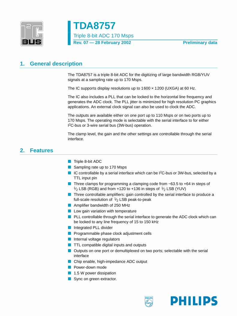
TDA8757 Triple 8-bit ADC 170 Msps Rev. 07 — 28 February 2002 Preliminary data 1. General description The TDA8757 is a triple 8-bit ADC for the digitizing of large bandwidth RGB/YUV signals at a sampling rate up to 170 Msps. The IC supports display resolutions up to 1 600 × 1200 (UXGA) at 60 Hz. The IC also includes a PLL that can be locked to the horizontal line frequency and generates the ADC clock. The PLL jitter is minimized for high resolution PC graphics applications. An external clock signal can also be used to clock the ADC. The outputs are available either on one port up to 110 Msps or on two ports up to 170 Msps. The operating mode is selectable with the serial interface to for either I 2 C-bus or 3-wire serial bus (3W-bus) operation. The clamp level, the gain and the other settings are controllable through the serial interface. 2. Features ■ Triple 8-bit ADC ■ Sampling rate up to 170 Msps ■ IC controllable by a serial interface which can be I 2 C-bus or 3W-bus, selected by a TTL input pin ■ Three clamps for programming a clamping code from -63.5 to +64 in steps of 1 ∕ 2 LSB (RGB) and from +120 to +136 in steps of 1 ∕ 2 LSB (YUV) ■ Three controllable amplifiers: gain controlled by the serial interface to produce a full-scale resolution of 1 ∕ 2 LSB peak-to-peak ■ Amplifier bandwidth of 250 MHz ■ Low gain variation with temperature ■ PLL controllable through the serial interface to generate the ADC clock which can be locked to any line frequency of 15 to 150 kHz ■ Integrated PLL divider ■ Programmable phase clock adjustment cells ■ Internal voltage regulators ■ TTL compatible digital inputs and outputs ■ Outputs on one port or demultiplexed on two ports; selectable with the serial interface ■ Chip enable, high-impedance ADC output ■ Power-down mode ■ 1.5 W power dissipation ■ Sync on green extractor.

Welcome message from author
This document is posted to help you gain knowledge. Please leave a comment to let me know what you think about it! Share it to your friends and learn new things together.
Transcript
TDA8757Triple 8-bit ADC 170 MspsRev. 07 — 28 February 2002 Preliminary data
1. General description
The TDA8757 is a triple 8-bit ADC for the digitizing of large bandwidth RGB/YUVsignals at a sampling rate up to 170 Msps.
The IC supports display resolutions up to 1600 × 1200 (UXGA) at 60 Hz.
The IC also includes a PLL that can be locked to the horizontal line frequency andgenerates the ADC clock. The PLL jitter is minimized for high resolution PC graphicsapplications. An external clock signal can also be used to clock the ADC.
The outputs are available either on one port up to 110 Msps or on two ports up to170 Msps. The operating mode is selectable with the serial interface to for eitherI2C-bus or 3-wire serial bus (3W-bus) operation.
The clamp level, the gain and the other settings are controllable through the serialinterface.
2. Features
Triple 8-bit ADC
Sampling rate up to 170 Msps
IC controllable by a serial interface which can be I2C-bus or 3W-bus, selected by aTTL input pin
Three clamps for programming a clamping code from −63.5 to +64 in steps of1⁄2 LSB (RGB) and from +120 to +136 in steps of 1⁄2 LSB (YUV)
Three controllable amplifiers: gain controlled by the serial interface to produce afull-scale resolution of 1⁄2 LSB peak-to-peak
Amplifier bandwidth of 250 MHz
Low gain variation with temperature
PLL controllable through the serial interface to generate the ADC clock which canbe locked to any line frequency of 15 to 150 kHz
Integrated PLL divider
Programmable phase clock adjustment cells
Internal voltage regulators
TTL compatible digital inputs and outputs
Outputs on one port or demultiplexed on two ports; selectable with the serialinterface
Chip enable, high-impedance ADC output
Power-down mode
1.5 W power dissipation
Sync on green extractor.
Philips Semiconductors TDA8757Triple 8-bit ADC 170 Msps
3. Applications
RGB/YUV high-speed digitizing
LCD panels drive
LCD projection systems
VGA to UXGA (1600 × 1200 at 60 Hz) modes.
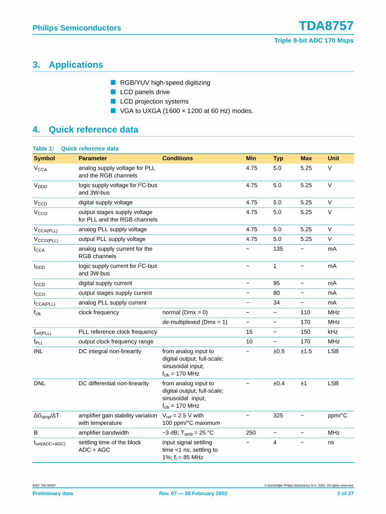
4. Quick reference data
Table 1: Quick reference data
Symbol Parameter Conditions Min Typ Max Unit
VCCA analog supply voltage for PLLand the RGB channels
4.75 5.0 5.25 V
VDDD logic supply voltage for I2C-busand 3W-bus
4.75 5.0 5.25 V
VCCD digital supply voltage 4.75 5.0 5.25 V
VCCO output stages supply voltagefor PLL and the RGB channels
4.75 5.0 5.25 V
VCCA(PLL) analog PLL supply voltage 4.75 5.0 5.25 V
VCCO(PLL) output PLL supply voltage 4.75 5.0 5.25 V
ICCA analog supply current for theRGB channels
− 135 − mA
IDDD logic supply current for I2C-busand 3W-bus
− 1 − mA
ICCD digital supply current − 95 − mA
ICCO output stages supply current − 80 − mA
ICCA(PLL) analog PLL supply current − 34 − mA
fclk clock frequency normal (Dmx = 0) − − 110 MHz
de-multiplexed (Dmx = 1) − − 170 MHz
fref(PLL) PLL reference clock frequency 15 − 150 kHz
fPLL output clock frequency range 10 − 170 MHz
INL DC integral non-linearity from analog input todigital output; full-scale;sinusoidal input;fclk = 170 MHz
− ±0.5 ±1.5 LSB
DNL DC differential non-linearity from analog input todigital output; full-scale;sinusoidal input;fclk = 170 MHz
− ±0.4 ±1 LSB
∆Gamp/∆T amplifier gain stability variationwith temperature
Vref = 2.5 V with100 ppm/°C maximum
− 325 − ppm/°C
B amplifier bandwidth −3 dB; Tamb = 25 °C 250 − − MHz
tset(ADC+AGC) settling time of the blockADC + AGC
input signal settlingtime <1 ns; settling to1%; fi = 85 MHz
− 4 − ns
Preliminary data Rev. 07 — 28 February 2002 2 of 37
9397 750 09457 © Koninklijke Philips Electronics N.V. 2002. All rights reserved.
Philips Semiconductors TDA8757Triple 8-bit ADC 170 Msps
5. Ordering information
DRPLL PLL divider ratio 100 − 4095
Ptot total power dissipation fclk = 170 MHz;sinusoidalinput
− 1.5 − W
jPLL(max)(p-p) maximum PLL phase jitter(peak-to-peak value)
fclk = 170 MHz − 360 − ps
Table 1: Quick reference data …continued
Symbol Parameter Conditions Min Typ Max Unit
Table 2: Ordering information
Type number Package
Name Description Version
TDA8757HL HLQFP144 plastic, heatsink low profile quad flat package; 144 leads;body 20 × 20 × 1.4 mm
SOT612-1
Preliminary data Rev. 07 — 28 February 2002 3 of 37
9397 750 09457 © Koninklijke Philips Electronics N.V. 2002. All rights reserved.
Philips Semiconductors TDA8757Triple 8-bit ADC 170 Msps
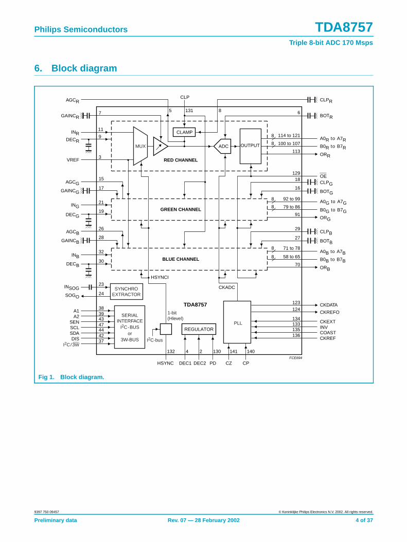
6. Block diagram
Fig 1. Block diagram.
FCE694
ADC
REGULATOR
CLAMP
RED CHANNEL
A0R to A7R
CLPRCLP
7
11
9
3
15
17
21
19
26
28
32
30
38394347444237
132 4 2 130 141 140
136135133134
124123
70
71 to 78
58 to 65
27
29
91
79 to 86
92 to 99
16
18129
113
100 to 107
114 to 121
681315
B0R to B7RORR
GREEN CHANNEL
BLUE CHANNEL
TDA8757
OUTPUT
GAINCR BOTR
A0G to A7G
CLPG
B0G to B7GORG
BOTG
A0B to A7B
CLPB
B0B to B7BORB
8
8
8
8
8
8
CKADC
HSYNCI
CKDATA
CKREFO
CKEXTINVCOASTCKREF
BOTB
OE
DEC1HSYNC DEC2 PD CZ CP
AGCR
INRDECR
GAINCG
AGCG
ING
DECG
GAINCB
AGCB
INB
INSOG
SOGO
DECB
VREF
A1A2
SENSCLSDADIS
I2C/3W
SERIALINTERFACE
I2C-BUSor
3W-BUS
SYNCHROEXTRACTOR
23
24
MUX
I2C-bus
PLL
1-bit(Hlevel)
Preliminary data Rev. 07 — 28 February 2002 4 of 37
9397 750 09457 © Koninklijke Philips Electronics N.V. 2002. All rights reserved.
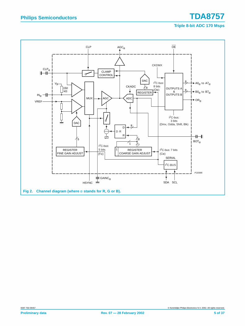
Philips Semiconductors TDA8757Triple 8-bit ADC 170 Msps
Fig 2. Channel diagram (where α stands for R, G or B).
FCE695
DAC
REGISTERFINE GAIN ADJUST
DAC
ADC
REGISTERCOARSE GAIN ADJUST
CLAMPCONTROL
REGISTER
MUX AGC
D RD
R
8
8
8 A0α to A7α
B0α to B7α
ORα
150kΩ
OUTPUTS A&
OUTPUTS B
85
GAINCα
8
BOTα
OE
CKADC
AGCαCLP
CLPα
HSYNC SDA SCL
INα
VREF
VP
SERIAL
71
1I2C-bus:5 bits I2C-bus: 7 bits
(Cα)
I2C-bus:8 bits(Oα)
I2C-bus:3 bits
(Dmx, Odda, Shift, Blk)
I2C-BUS
(Fα)
CKDMX
Preliminary data Rev. 07 — 28 February 2002 5 of 37
9397 750 09457 © Koninklijke Philips Electronics N.V. 2002. All rights reserved.
Philips Semiconductors TDA8757Triple 8-bit ADC 170 Msps
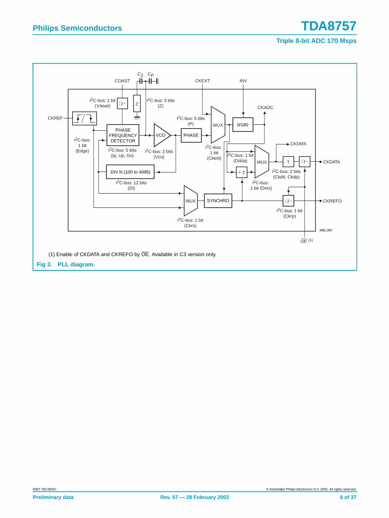
(1) Enable of CKDATA and CKREFO by OE. Available in C3 version only.
Fig 3. PLL diagram.
MBL365
PHASEFREQUENCYDETECTOR
PHASE
I2C-bus: 1 bit(Vlevel)
I2C-bus: 3 bits(Z)
I2C-bus: 1 bit
(Ckext)I2C-bus: 1 bit
(Odda)
I2C-bus: 5 bits(Ip, Up, Do)
I2C-bus: 5 bits(P)
I2C-bus: 2 bits(Vco)
I2C-bus: 12 bits(Di)
I2C-bus: 2 bits(Ckdd, Ckdp)
SYNCHRO
DIV N (100 to 4095)
0/180
VCO
MUX
÷ 2
τ +/−MUX
MUX
CKADC
OE (1)
I2C-bus: 1 bit(Ckrp)
I2C-bus: 1 bit(Ckrs)
I2C-bus:1 bit
(Edge)
CKREFO
CKREF
COAST CKEXT
Z
INV
CZ CP
CKDATA
I2C-bus: 1 bit (Dmx)
CKDMX
+/−
+/−
Preliminary data Rev. 07 — 28 February 2002 6 of 37
9397 750 09457 © Koninklijke Philips Electronics N.V. 2002. All rights reserved.
Philips Semiconductors TDA8757Triple 8-bit ADC 170 Msps
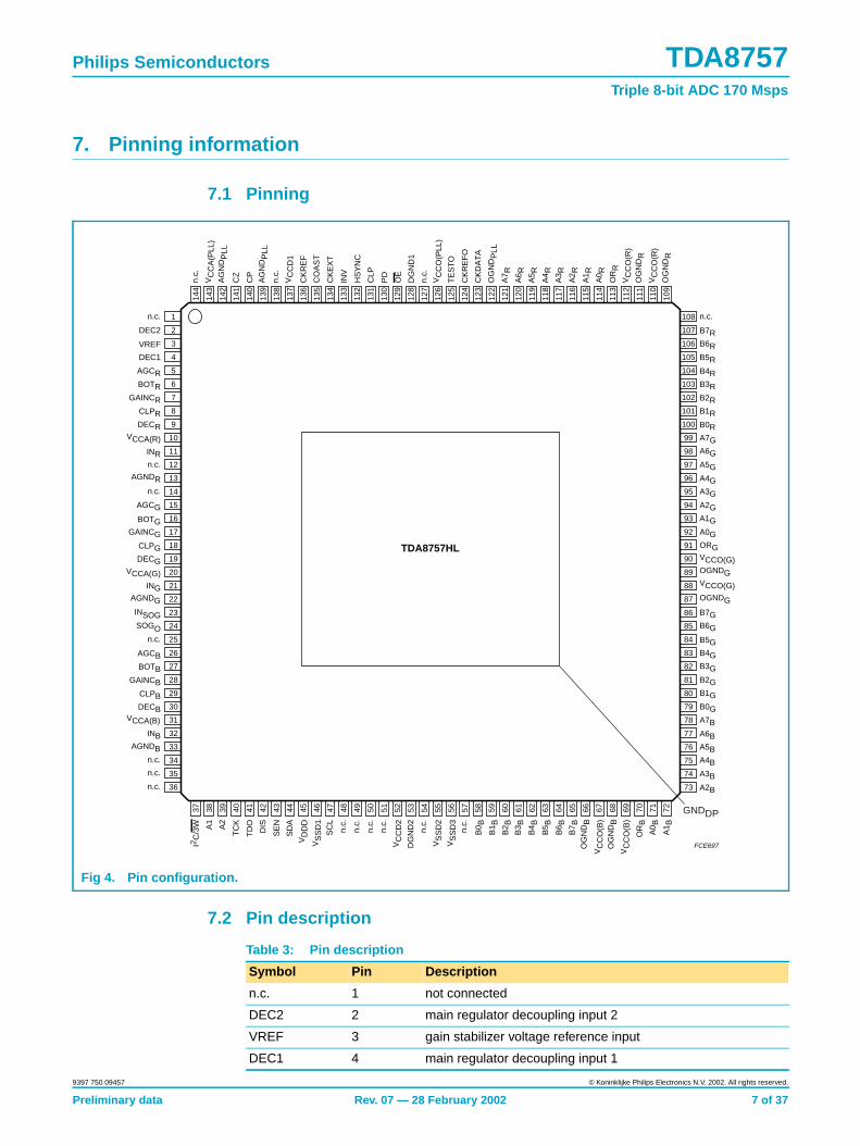
7. Pinning information
7.1 Pinning
7.2 Pin description
Fig 4. Pin configuration.
FCE697
TDA8757HL
1
2
3
4
5
6
7
8
9
10
11
12
13
14
15
16
17
18
19
20
21
22
23
24
25
26
27
28
29
30
31
32
33
34
35
36
108
107
106
105
104
103
102
101
100
99
98
97
96
95
94
93
92
91
90
89
88
87
86
85
84
83
82
81
80
79
78
77
76
75
74
73
37 38 39 40 41 42 43 44 45 46 47 48 49 50 51 52 53 54 55 56 57 58 59 60 61 62 63 64 65 66 67 68 69 70 71 72
144
143
142
141
140
139
138
137
136
135
134
133
132
131
130
129
128
127
126
125
124
123
122
121
120
119
118
117
116
115
114
113
112
111
110
109
n.c.
DEC2
VREF
DEC1
AGCRBOTR
GAINCRCLPRDECR
VCCA(R)
INRn.c.
AGNDRn.c.
AGCG
BOTGGAINCG
CLPGDECG
ING
INSOGSOGO
n.c.
AGCBBOTB
GAINCBCLPBDECB
VCCA(B)
INBAGNDB
n.c.
n.c.
n.c.
VCCA(G)
AGNDG
I2C
/3W A1
A2
TC
K
TD
O
DIS
SE
N
SD
A
VD
DD
VS
SD
1S
CL
n.c.
n.c.
n.c.
n.c.
VC
CD
2
DG
ND
2
n.c.
VS
SD
2V
SS
D3
n.c.
B0 B
B1 B
B2 B
B3 B
B4 B
B5 B
B6 B
B7 B
OG
ND
B
OG
ND
BV
CC
O(B
)
VC
CO
(B)
OR
BA
0 BA
1 B
n.c.
B7RB6RB5RB4RB3RB2RB1RB0RA7GA6GA5GA4GA3GA2GA1GA0GORGVCCO(G)OGNDGVCCO(G)
OGNDG
B7GB6GB5GB4GB3GB2GB1GB0GA7BA6BA5BA4BA3BA2B
n.c.
VC
CA
(PLL
)A
GN
DP
LL
CZ
CP
AG
ND
PLL
n.c.
VC
CD
1
CK
RE
F
CO
AS
T
CK
EX
T
INV
HS
YN
C
CLP
PD
OE
DG
ND
1
n.c.
VC
CO
(PLL
)
TE
ST
O
CK
RE
FO
CK
DA
TA
OG
ND
PLL
A7 R
A6 R
A5 R
A4 R
A3 R
A2 R
A1 R
A0 R
OR
RV
CC
O(R
)O
GN
DR
VC
CO
(R)
OG
ND
R
GNDDP
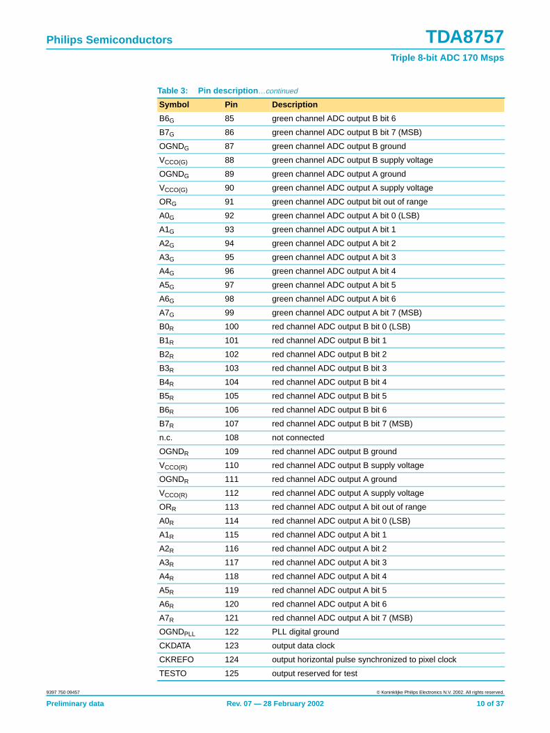
Table 3: Pin description
Symbol Pin Description
n.c. 1 not connected
DEC2 2 main regulator decoupling input 2
VREF 3 gain stabilizer voltage reference input
DEC1 4 main regulator decoupling input 1
Preliminary data Rev. 07 — 28 February 2002 7 of 37
9397 750 09457 © Koninklijke Philips Electronics N.V. 2002. All rights reserved.
Philips Semiconductors TDA8757Triple 8-bit ADC 170 Msps
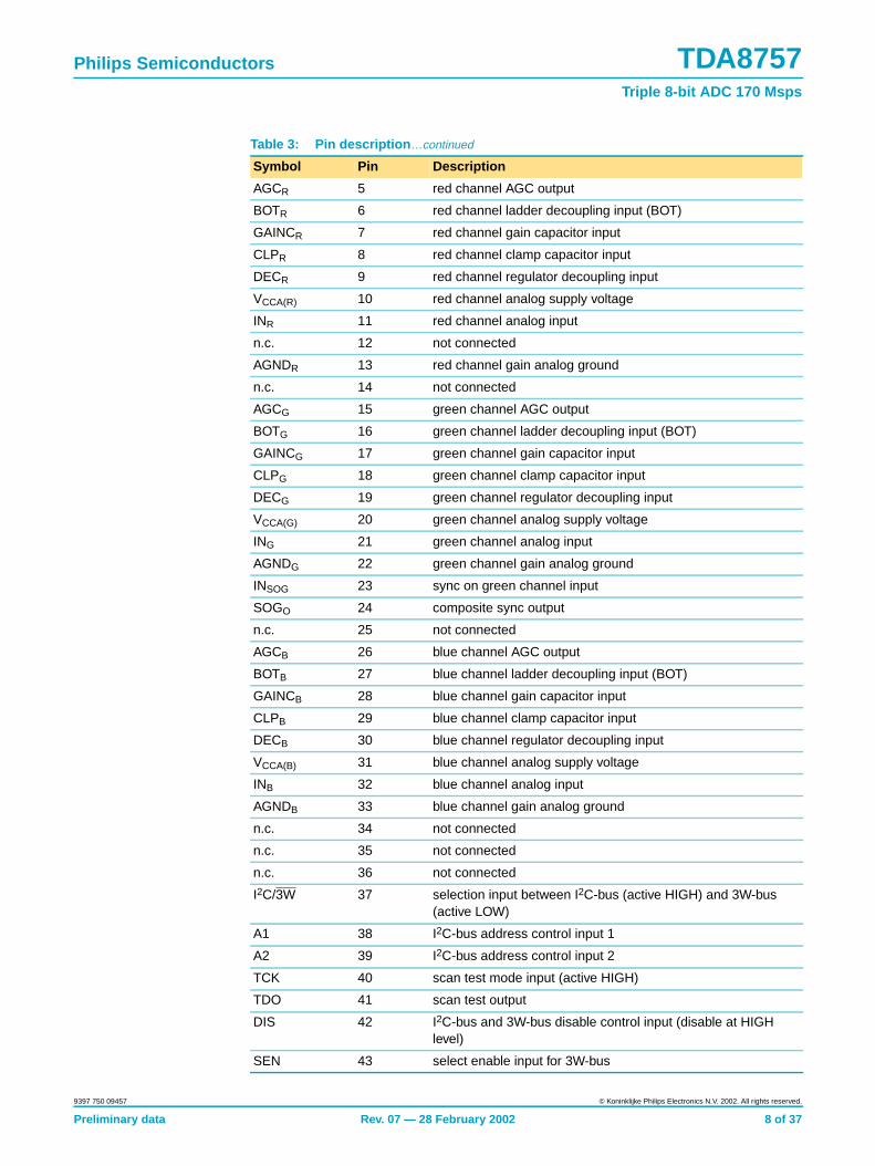
AGCR 5 red channel AGC output
BOTR 6 red channel ladder decoupling input (BOT)
GAINCR 7 red channel gain capacitor input
CLPR 8 red channel clamp capacitor input
DECR 9 red channel regulator decoupling input
VCCA(R) 10 red channel analog supply voltage
INR 11 red channel analog input
n.c. 12 not connected
AGNDR 13 red channel gain analog ground
n.c. 14 not connected
AGCG 15 green channel AGC output
BOTG 16 green channel ladder decoupling input (BOT)
GAINCG 17 green channel gain capacitor input
CLPG 18 green channel clamp capacitor input
DECG 19 green channel regulator decoupling input
VCCA(G) 20 green channel analog supply voltage
ING 21 green channel analog input
AGNDG 22 green channel gain analog ground
INSOG 23 sync on green channel input
SOGO 24 composite sync output
n.c. 25 not connected
AGCB 26 blue channel AGC output
BOTB 27 blue channel ladder decoupling input (BOT)
GAINCB 28 blue channel gain capacitor input
CLPB 29 blue channel clamp capacitor input
DECB 30 blue channel regulator decoupling input
VCCA(B) 31 blue channel analog supply voltage
INB 32 blue channel analog input
AGNDB 33 blue channel gain analog ground
n.c. 34 not connected
n.c. 35 not connected
n.c. 36 not connected
I2C/3W 37 selection input between I2C-bus (active HIGH) and 3W-bus(active LOW)
A1 38 I2C-bus address control input 1
A2 39 I2C-bus address control input 2
TCK 40 scan test mode input (active HIGH)
TDO 41 scan test output
DIS 42 I2C-bus and 3W-bus disable control input (disable at HIGHlevel)
SEN 43 select enable input for 3W-bus
Table 3: Pin description …continued
Symbol Pin Description
Preliminary data Rev. 07 — 28 February 2002 8 of 37
9397 750 09457 © Koninklijke Philips Electronics N.V. 2002. All rights reserved.
Philips Semiconductors TDA8757Triple 8-bit ADC 170 Msps
SDA 44 I2C-bus/3W-bus serial data input
VDDD 45 logic I2C-bus/3W-bus digital supply voltage
VSSD1 46 logic I2C-bus/3W-bus digital ground 1
SCL 47 I2C-bus/3W-bus serial clock input
n.c. 48 not connected
n.c. 49 not connected
n.c. 50 not connected
n.c. 51 not connected
VCCD2 52 digital supply voltage 2
DGND2 53 digital ground 2
n.c. 54 not connected
VSSD2 55 logic I2C-bus/3W-bus digital ground 2
VSSD3 56 logic I2C-bus/3W-bus digital ground 3
n.c. 57 not connected
B0B 58 blue channel ADC output B bit 0 (LSB)
B1B 59 blue channel ADC output B bit 1
B2B 60 blue channel ADC output B bit 2
B3B 61 blue channel ADC output B bit 3
B4B 62 blue channel ADC output B bit 4
B5B 63 blue channel ADC output B bit 5
B6B 64 blue channel ADC output B bit 6
B7B 65 blue channel ADC output B bit 7 (MSB)
OGNDB 66 blue channel ADC output B ground
VCCO(B) 67 blue channel ADC output B supply voltage
OGNDB 68 blue channel ADC output A ground
VCCO(B) 69 blue channel ADC output A supply voltage
ORB 70 blue channel ADC output bit out of range
A0B 71 blue channel ADC output A bit 0 (LSB)
A1B 72 blue channel ADC output A bit 1
A2B 73 blue channel ADC output A bit 2
A3B 74 blue channel ADC output A bit 3
A4B 75 blue channel ADC output A bit 4
A5B 76 blue channel ADC output A bit 5
A6B 77 blue channel ADC output A bit 6
A7B 78 blue channel ADC output A bit 7 (MSB)
B0G 79 green channel ADC output B bit 0 (LSB)
B1G 80 green channel ADC output B bit 1
B2G 81 green channel ADC output B bit 2
B3G 82 green channel ADC output B bit 3
B4G 83 green channel ADC output B bit 4
B5G 84 green channel ADC output B bit 5
Table 3: Pin description …continued
Symbol Pin Description
Preliminary data Rev. 07 — 28 February 2002 9 of 37
9397 750 09457 © Koninklijke Philips Electronics N.V. 2002. All rights reserved.
Philips Semiconductors TDA8757Triple 8-bit ADC 170 Msps
B6G 85 green channel ADC output B bit 6
B7G 86 green channel ADC output B bit 7 (MSB)
OGNDG 87 green channel ADC output B ground
VCCO(G) 88 green channel ADC output B supply voltage
OGNDG 89 green channel ADC output A ground
VCCO(G) 90 green channel ADC output A supply voltage
ORG 91 green channel ADC output bit out of range
A0G 92 green channel ADC output A bit 0 (LSB)
A1G 93 green channel ADC output A bit 1
A2G 94 green channel ADC output A bit 2
A3G 95 green channel ADC output A bit 3
A4G 96 green channel ADC output A bit 4
A5G 97 green channel ADC output A bit 5
A6G 98 green channel ADC output A bit 6
A7G 99 green channel ADC output A bit 7 (MSB)
B0R 100 red channel ADC output B bit 0 (LSB)
B1R 101 red channel ADC output B bit 1
B2R 102 red channel ADC output B bit 2
B3R 103 red channel ADC output B bit 3
B4R 104 red channel ADC output B bit 4
B5R 105 red channel ADC output B bit 5
B6R 106 red channel ADC output B bit 6
B7R 107 red channel ADC output B bit 7 (MSB)
n.c. 108 not connected
OGNDR 109 red channel ADC output B ground
VCCO(R) 110 red channel ADC output B supply voltage
OGNDR 111 red channel ADC output A ground
VCCO(R) 112 red channel ADC output A supply voltage
ORR 113 red channel ADC output A bit out of range
A0R 114 red channel ADC output A bit 0 (LSB)
A1R 115 red channel ADC output A bit 1
A2R 116 red channel ADC output A bit 2
A3R 117 red channel ADC output A bit 3
A4R 118 red channel ADC output A bit 4
A5R 119 red channel ADC output A bit 5
A6R 120 red channel ADC output A bit 6
A7R 121 red channel ADC output A bit 7 (MSB)
OGNDPLL 122 PLL digital ground
CKDATA 123 output data clock
CKREFO 124 output horizontal pulse synchronized to pixel clock
TESTO 125 output reserved for test
Table 3: Pin description …continued
Symbol Pin Description
Preliminary data Rev. 07 — 28 February 2002 10 of 37
9397 750 09457 © Koninklijke Philips Electronics N.V. 2002. All rights reserved.
Philips Semiconductors TDA8757Triple 8-bit ADC 170 Msps
8. Functional description
This triple high-speed 8-bit ADC is designed to convert RGB/YUV signals, comingfrom an analog source, into digital data used by a LCD driver (pixel clock up to170 MHz).
8.1 Analog video inputs
The RGB/YUV video inputs are externally AC coupled and are internallyDC polarized.
The synchronization signals are also used for the internal PLL and the gaincalibration.
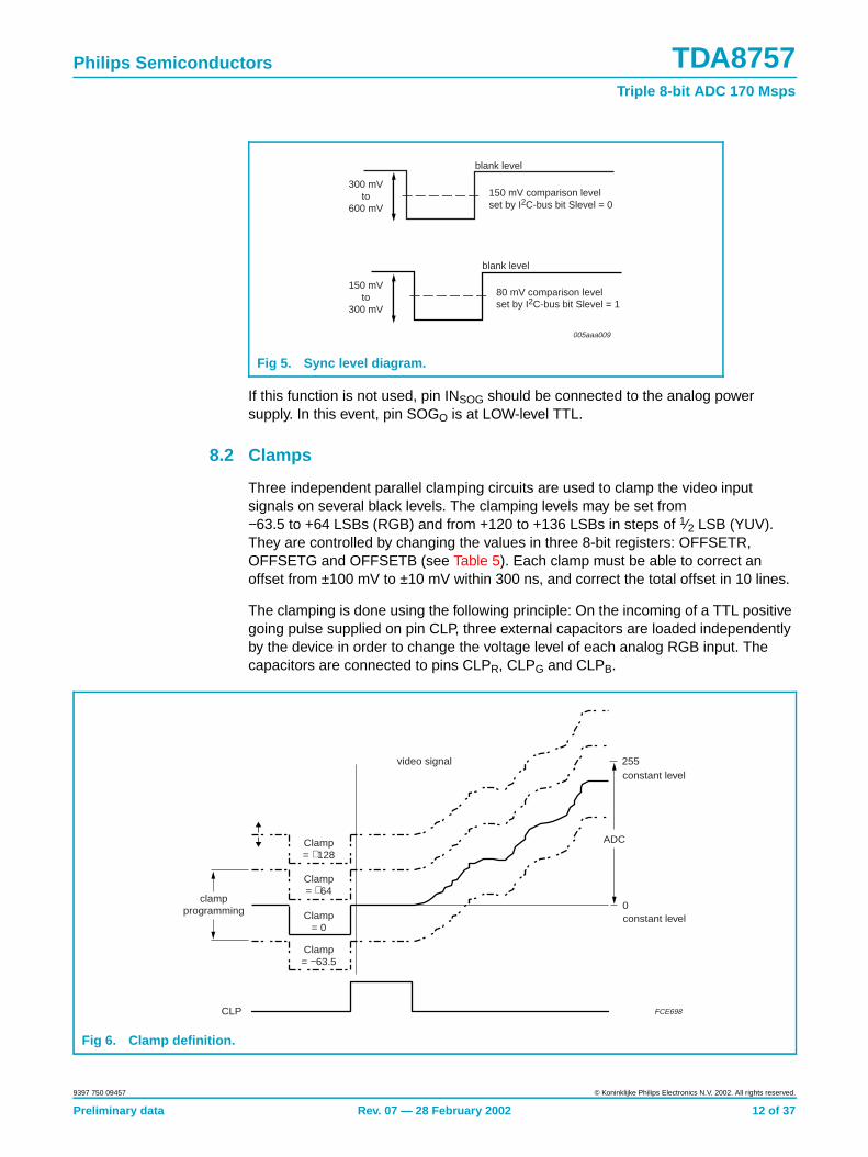
If the green video signal has composite sync (sync on green), it is possible to extractthis composite sync by connecting the green signal to pin INSOG (AC coupled). Whenthe sync pulse amplitude is below 300 mV, the I2C-bus bit ‘Slevel’ has to be set tologic 1 (see Figure 5). The maximum amplitude for the sync pulse is 600 mV.
The composite sync is available at pin SOGO (TTL level compatible signal).
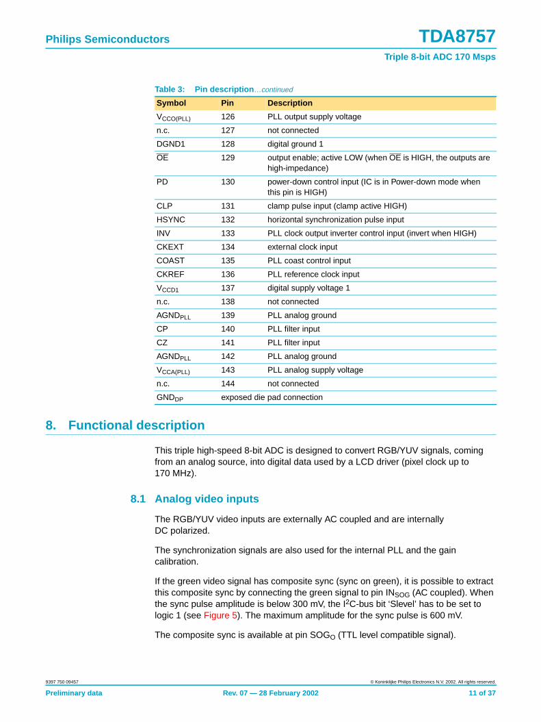
VCCO(PLL) 126 PLL output supply voltage
n.c. 127 not connected
DGND1 128 digital ground 1
OE 129 output enable; active LOW (when OE is HIGH, the outputs arehigh-impedance)
PD 130 power-down control input (IC is in Power-down mode whenthis pin is HIGH)
CLP 131 clamp pulse input (clamp active HIGH)
HSYNC 132 horizontal synchronization pulse input
INV 133 PLL clock output inverter control input (invert when HIGH)
CKEXT 134 external clock input
COAST 135 PLL coast control input
CKREF 136 PLL reference clock input
VCCD1 137 digital supply voltage 1
n.c. 138 not connected
AGNDPLL 139 PLL analog ground
CP 140 PLL filter input
CZ 141 PLL filter input
AGNDPLL 142 PLL analog ground
VCCA(PLL) 143 PLL analog supply voltage
n.c. 144 not connected
GNDDP exposed die pad connection
Table 3: Pin description …continued
Symbol Pin Description
Preliminary data Rev. 07 — 28 February 2002 11 of 37
9397 750 09457 © Koninklijke Philips Electronics N.V. 2002. All rights reserved.
Philips Semiconductors TDA8757Triple 8-bit ADC 170 Msps
If this function is not used, pin INSOG should be connected to the analog powersupply. In this event, pin SOGO is at LOW-level TTL.
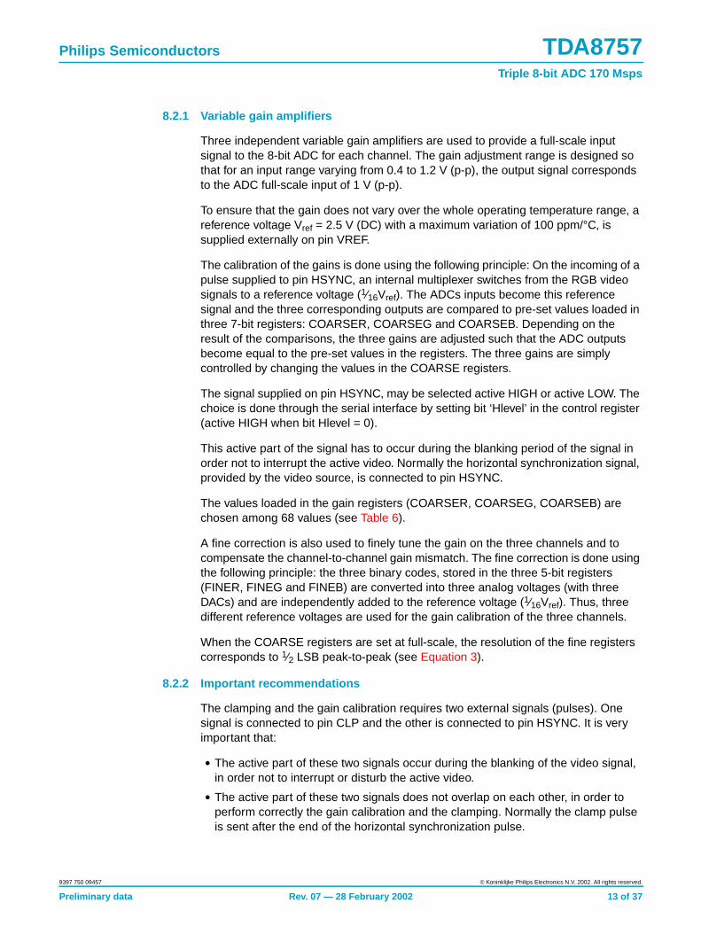
8.2 Clamps
Three independent parallel clamping circuits are used to clamp the video inputsignals on several black levels. The clamping levels may be set from−63.5 to +64 LSBs (RGB) and from +120 to +136 LSBs in steps of 1⁄2 LSB (YUV).They are controlled by changing the values in three 8-bit registers: OFFSETR,OFFSETG and OFFSETB (see Table 5). Each clamp must be able to correct anoffset from ±100 mV to ±10 mV within 300 ns, and correct the total offset in 10 lines.
The clamping is done using the following principle: On the incoming of a TTL positivegoing pulse supplied on pin CLP, three external capacitors are loaded independentlyby the device in order to change the voltage level of each analog RGB input. Thecapacitors are connected to pins CLPR, CLPG and CLPB.
Fig 5. Sync level diagram.
blank level
150 mV comparison levelset by I2C-bus bit Slevel = 0
blank level
80 mV comparison levelset by I2C-bus bit Slevel = 1
150 mVto
300 mV
300 mVto
600 mV
005aaa009
Fig 6. Clamp definition.
video signal
CLP
Clamp= +128
Clamp= +64
Clamp= −63.5
Clamp= 0
0constant level
255constant level
FCE698
clampprogramming
ADC
Preliminary data Rev. 07 — 28 February 2002 12 of 37
9397 750 09457 © Koninklijke Philips Electronics N.V. 2002. All rights reserved.
Philips Semiconductors TDA8757Triple 8-bit ADC 170 Msps
8.2.1 Variable gain amplifiers
Three independent variable gain amplifiers are used to provide a full-scale inputsignal to the 8-bit ADC for each channel. The gain adjustment range is designed sothat for an input range varying from 0.4 to 1.2 V (p-p), the output signal correspondsto the ADC full-scale input of 1 V (p-p).
To ensure that the gain does not vary over the whole operating temperature range, areference voltage Vref = 2.5 V (DC) with a maximum variation of 100 ppm/°C, issupplied externally on pin VREF.
The calibration of the gains is done using the following principle: On the incoming of apulse supplied to pin HSYNC, an internal multiplexer switches from the RGB videosignals to a reference voltage (1⁄16Vref). The ADCs inputs become this referencesignal and the three corresponding outputs are compared to pre-set values loaded inthree 7-bit registers: COARSER, COARSEG and COARSEB. Depending on theresult of the comparisons, the three gains are adjusted such that the ADC outputsbecome equal to the pre-set values in the registers. The three gains are simplycontrolled by changing the values in the COARSE registers.
The signal supplied on pin HSYNC, may be selected active HIGH or active LOW. Thechoice is done through the serial interface by setting bit ‘Hlevel’ in the control register(active HIGH when bit Hlevel = 0).
This active part of the signal has to occur during the blanking period of the signal inorder not to interrupt the active video. Normally the horizontal synchronization signal,provided by the video source, is connected to pin HSYNC.
The values loaded in the gain registers (COARSER, COARSEG, COARSEB) arechosen among 68 values (see Table 6).
A fine correction is also used to finely tune the gain on the three channels and tocompensate the channel-to-channel gain mismatch. The fine correction is done usingthe following principle: the three binary codes, stored in the three 5-bit registers(FINER, FINEG and FINEB) are converted into three analog voltages (with threeDACs) and are independently added to the reference voltage (1⁄16Vref). Thus, threedifferent reference voltages are used for the gain calibration of the three channels.
When the COARSE registers are set at full-scale, the resolution of the fine registerscorresponds to 1⁄2 LSB peak-to-peak (see Equation 3).
8.2.2 Important recommendations
The clamping and the gain calibration requires two external signals (pulses). Onesignal is connected to pin CLP and the other is connected to pin HSYNC. It is veryimportant that:
• The active part of these two signals occur during the blanking of the video signal,in order not to interrupt or disturb the active video.
• The active part of these two signals does not overlap on each other, in order toperform correctly the gain calibration and the clamping. Normally the clamp pulseis sent after the end of the horizontal synchronization pulse.
Preliminary data Rev. 07 — 28 February 2002 13 of 37
9397 750 09457 © Koninklijke Philips Electronics N.V. 2002. All rights reserved.
Philips Semiconductors TDA8757Triple 8-bit ADC 170 Msps
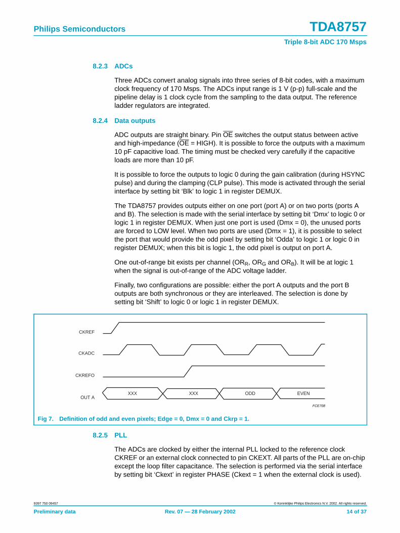
8.2.3 ADCs
Three ADCs convert analog signals into three series of 8-bit codes, with a maximumclock frequency of 170 Msps. The ADCs input range is 1 V (p-p) full-scale and thepipeline delay is 1 clock cycle from the sampling to the data output. The referenceladder regulators are integrated.
8.2.4 Data outputs
ADC outputs are straight binary. Pin OE switches the output status between activeand high-impedance (OE = HIGH). It is possible to force the outputs with a maximum10 pF capacitive load. The timing must be checked very carefully if the capacitiveloads are more than 10 pF.
It is possible to force the outputs to logic 0 during the gain calibration (during HSYNCpulse) and during the clamping (CLP pulse). This mode is activated through the serialinterface by setting bit ‘Blk’ to logic 1 in register DEMUX.
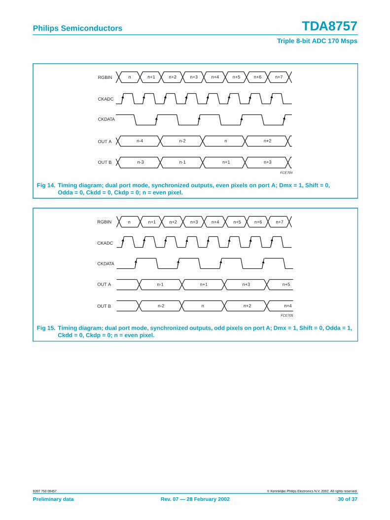
The TDA8757 provides outputs either on one port (port A) or on two ports (ports Aand B). The selection is made with the serial interface by setting bit ‘Dmx’ to logic 0 orlogic 1 in register DEMUX. When just one port is used (Dmx = 0), the unused portsare forced to LOW level. When two ports are used (Dmx = 1), it is possible to selectthe port that would provide the odd pixel by setting bit ‘Odda’ to logic 1 or logic 0 inregister DEMUX; when this bit is logic 1, the odd pixel is output on port A.
One out-of-range bit exists per channel (ORR, ORG and ORB). It will be at logic 1when the signal is out-of-range of the ADC voltage ladder.
Finally, two configurations are possible: either the port A outputs and the port Boutputs are both synchronous or they are interleaved. The selection is done bysetting bit ‘Shift’ to logic 0 or logic 1 in register DEMUX.
8.2.5 PLL
The ADCs are clocked by either the internal PLL locked to the reference clockCKREF or an external clock connected to pin CKEXT. All parts of the PLL are on-chipexcept the loop filter capacitance. The selection is performed via the serial interfaceby setting bit ‘Ckext’ in register PHASE (Ckext = 1 when the external clock is used).
Fig 7. Definition of odd and even pixels; Edge = 0, Dmx = 0 and Ckrp = 1.
FCE708
CKADC
CKREF
CKREFO
OUT AXXX ODD EVENXXX
Preliminary data Rev. 07 — 28 February 2002 14 of 37
9397 750 09457 © Koninklijke Philips Electronics N.V. 2002. All rights reserved.
Philips Semiconductors TDA8757Triple 8-bit ADC 170 Msps
The reference clock (CKREF) range is between 15 and 150 kHz. Consequently, theVCO minimum frequency is 12 MHz and the maximum frequency is 170 MHz. Thegain of the VCO part can be controlled through the serial interface, depending on thefrequency range to which the PLL is locked.
Moreover, the PLL may be locked either on the rising or on the falling edge of theCKREF signal pulses. This choice is made through the serial interface by settingbit ‘Edge’ in register CONTROL (rising edge when bit ‘Edge’ = 0).
The charge pump current (Icp) enables an increase of PLL bandwidth. It isprogrammable through the serial interface by setting bits ‘Ip2’, ‘Ip1’ and ‘Ip0’ in thecontrol register (see Table 8).
Different resistance values (R) for the filter can also be programmed through theserial interface by setting the bits ‘Z2’, ‘Z1’ and ‘Z0’ in register VCO (see Table 9).
To have optimal PLL performance, R and Icp must be chosen so that:
• The result of the product ‘R × Icp’ is smaller than a determined limit (Lim)
• The result of the product ‘R × Icp’ is as close as possible to this limit (Lim).
(1)
where:
• DRPLL = the divider ratio, which is the ratio between the pixel frequency and thehorizontal line frequency of the incoming signal. The setting of this parameter isperformed through the serial interface with bits Di0 to Di11. These bits are presentin the VCO-, divider- and phase registers.
• fref = the frequency of the signal.
• K0 = the VCO gain, which depends on the pixel frequency ranges given inTable 10.
In the event that several combinations of R and Icp give the same result, a calculationof the damping factor (ξ) for each combination becomes necessary.
The combination of R and Icp whose damping factor is the closest to 1.5, generatesthe optimal PLL performance.
(2)
where CZ and CP are the external capacitors of the PLL loop filter. The recommendedvalues are: CZ = 68 nF and CP = 150 pF.
The COAST signal is used to disconnect the PLL phase frequency detector duringthe frame flyback (vertical blanking) or during the unavailability of the CKREF signal.This signal can normally be derived from the VSYNC signal.
COAST may be set either active HIGH or active LOW by setting bit ‘Vlevel’ in thecontrol register through the serial interface (Vlevel = 0 when HIGH).
Lim0.3π DRPLL× f ref×
K0--------------------------------------------------=
ξR CZ⋅
2---------------
K0 I cp⋅DRPLL CZ CP+( )⋅-----------------------------------------------⋅=
Preliminary data Rev. 07 — 28 February 2002 15 of 37
9397 750 09457 © Koninklijke Philips Electronics N.V. 2002. All rights reserved.
Philips Semiconductors TDA8757Triple 8-bit ADC 170 Msps
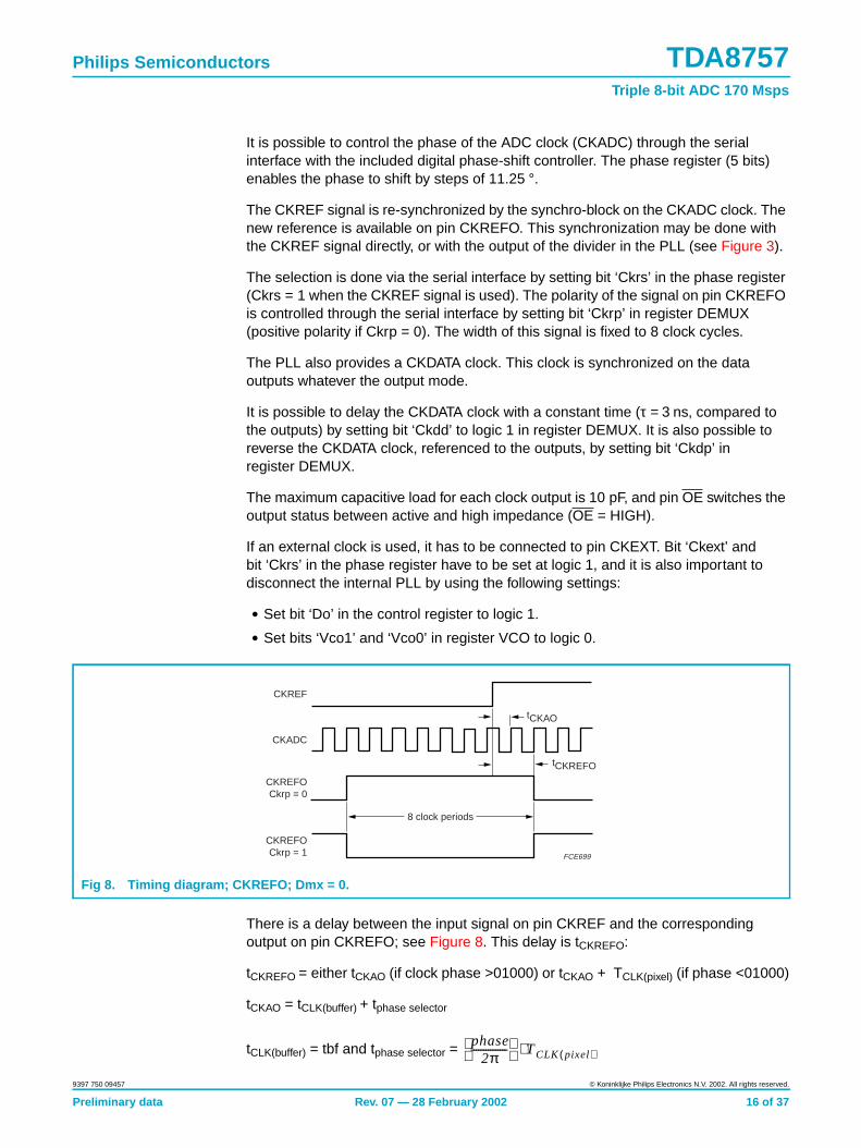
It is possible to control the phase of the ADC clock (CKADC) through the serialinterface with the included digital phase-shift controller. The phase register (5 bits)enables the phase to shift by steps of 11.25 °.
The CKREF signal is re-synchronized by the synchro-block on the CKADC clock. Thenew reference is available on pin CKREFO. This synchronization may be done withthe CKREF signal directly, or with the output of the divider in the PLL (see Figure 3).
The selection is done via the serial interface by setting bit ‘Ckrs’ in the phase register(Ckrs = 1 when the CKREF signal is used). The polarity of the signal on pin CKREFOis controlled through the serial interface by setting bit ‘Ckrp’ in register DEMUX(positive polarity if Ckrp = 0). The width of this signal is fixed to 8 clock cycles.
The PLL also provides a CKDATA clock. This clock is synchronized on the dataoutputs whatever the output mode.
It is possible to delay the CKDATA clock with a constant time (τ = 3 ns, compared tothe outputs) by setting bit ‘Ckdd’ to logic 1 in register DEMUX. It is also possible toreverse the CKDATA clock, referenced to the outputs, by setting bit ‘Ckdp’ inregister DEMUX.
The maximum capacitive load for each clock output is 10 pF, and pin OE switches theoutput status between active and high impedance (OE = HIGH).
If an external clock is used, it has to be connected to pin CKEXT. Bit ‘Ckext’ andbit ‘Ckrs’ in the phase register have to be set at logic 1, and it is also important todisconnect the internal PLL by using the following settings:
• Set bit ‘Do’ in the control register to logic 1.
• Set bits ‘Vco1’ and ‘Vco0’ in register VCO to logic 0.
There is a delay between the input signal on pin CKREF and the correspondingoutput on pin CKREFO; see Figure 8. This delay is tCKREFO:
tCKREFO = either tCKAO (if clock phase >01000) or tCKAO + TCLK(pixel) (if phase <01000)
tCKAO = tCLK(buffer) + tphase selector
tCLK(buffer) = tbf and tphase selector =
Fig 8. Timing diagram; CKREFO; Dmx = 0.
CKREF
CKADC
CKREFOCkrp = 0
CKREFOCkrp = 1
8 clock periods
FCE699
tCKAO
tCKREFO
phase2π---------------
TCLK pixel( )⋅
Preliminary data Rev. 07 — 28 February 2002 16 of 37
9397 750 09457 © Koninklijke Philips Electronics N.V. 2002. All rights reserved.
Philips Semiconductors TDA8757Triple 8-bit ADC 170 Msps
9. I2C-bus and 3W-bus interfaces
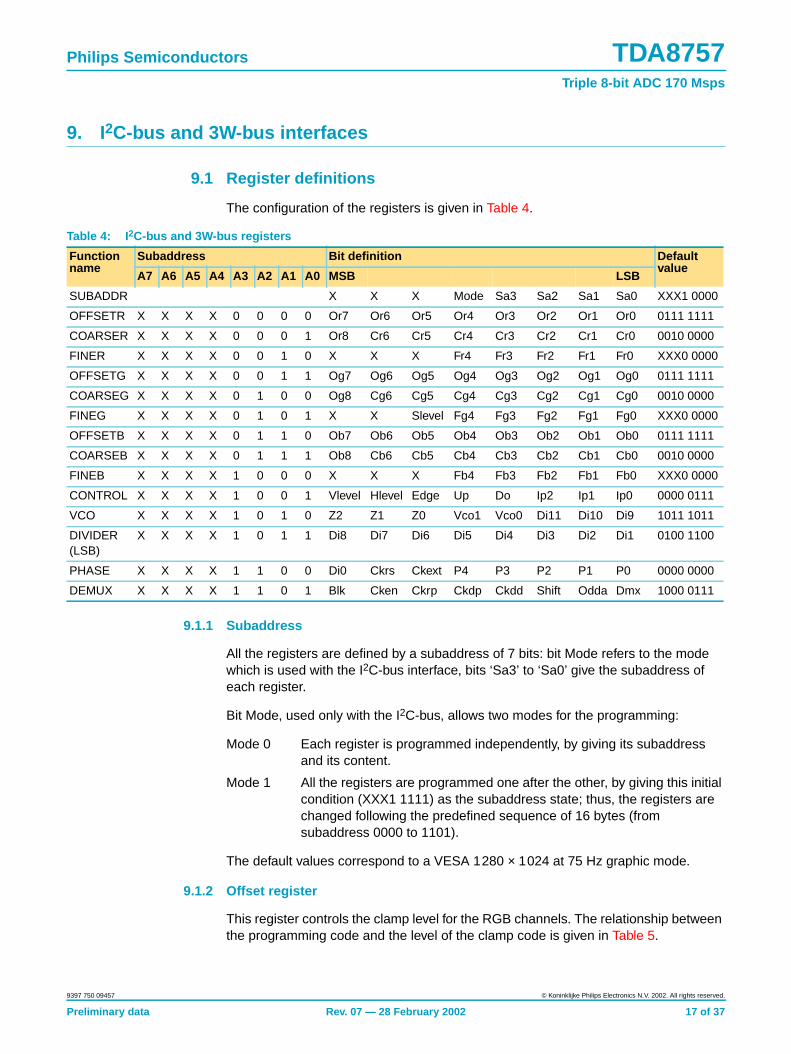
9.1 Register definitions
The configuration of the registers is given in Table 4.
9.1.1 Subaddress
All the registers are defined by a subaddress of 7 bits: bit Mode refers to the modewhich is used with the I2C-bus interface, bits ‘Sa3’ to ‘Sa0’ give the subaddress ofeach register.
Bit Mode, used only with the I2C-bus, allows two modes for the programming:
Mode 0 Each register is programmed independently, by giving its subaddressand its content.
Mode 1 All the registers are programmed one after the other, by giving this initialcondition (XXX1 1111) as the subaddress state; thus, the registers arechanged following the predefined sequence of 16 bytes (fromsubaddress 0000 to 1101).
The default values correspond to a VESA 1280 × 1024 at 75 Hz graphic mode.
9.1.2 Offset register
This register controls the clamp level for the RGB channels. The relationship betweenthe programming code and the level of the clamp code is given in Table 5.
Table 4: I 2C-bus and 3W-bus registers
Functionname
Subaddress Bit definition Defaultvalue
A7 A6 A5 A4 A3 A2 A1 A0 MSB LSB
SUBADDR X X X Mode Sa3 Sa2 Sa1 Sa0 XXX1 0000
OFFSETR X X X X 0 0 0 0 Or7 Or6 Or5 Or4 Or3 Or2 Or1 Or0 0111 1111
COARSER X X X X 0 0 0 1 Or8 Cr6 Cr5 Cr4 Cr3 Cr2 Cr1 Cr0 0010 0000
FINER X X X X 0 0 1 0 X X X Fr4 Fr3 Fr2 Fr1 Fr0 XXX0 0000
OFFSETG X X X X 0 0 1 1 Og7 Og6 Og5 Og4 Og3 Og2 Og1 Og0 0111 1111
COARSEG X X X X 0 1 0 0 Og8 Cg6 Cg5 Cg4 Cg3 Cg2 Cg1 Cg0 0010 0000
FINEG X X X X 0 1 0 1 X X Slevel Fg4 Fg3 Fg2 Fg1 Fg0 XXX0 0000
OFFSETB X X X X 0 1 1 0 Ob7 Ob6 Ob5 Ob4 Ob3 Ob2 Ob1 Ob0 0111 1111
COARSEB X X X X 0 1 1 1 Ob8 Cb6 Cb5 Cb4 Cb3 Cb2 Cb1 Cb0 0010 0000
FINEB X X X X 1 0 0 0 X X X Fb4 Fb3 Fb2 Fb1 Fb0 XXX0 0000
CONTROL X X X X 1 0 0 1 Vlevel Hlevel Edge Up Do Ip2 Ip1 Ip0 0000 0111
VCO X X X X 1 0 1 0 Z2 Z1 Z0 Vco1 Vco0 Di11 Di10 Di9 1011 1011
DIVIDER(LSB)
X X X X 1 0 1 1 Di8 Di7 Di6 Di5 Di4 Di3 Di2 Di1 0100 1100
PHASE X X X X 1 1 0 0 Di0 Ckrs Ckext P4 P3 P2 P1 P0 0000 0000
DEMUX X X X X 1 1 0 1 Blk Cken Ckrp Ckdp Ckdd Shift Odda Dmx 1000 0111
Preliminary data Rev. 07 — 28 February 2002 17 of 37
9397 750 09457 © Koninklijke Philips Electronics N.V. 2002. All rights reserved.
Philips Semiconductors TDA8757Triple 8-bit ADC 170 Msps
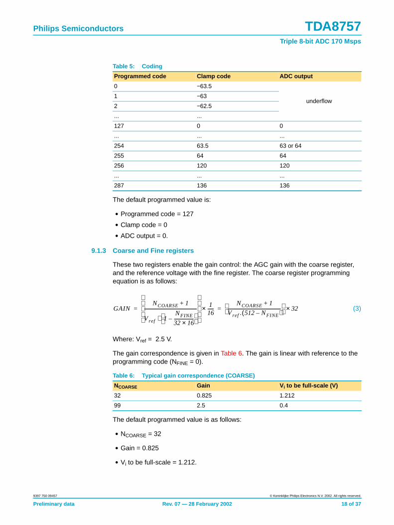
The default programmed value is:
• Programmed code = 127
• Clamp code = 0
• ADC output = 0.
9.1.3 Coarse and Fine registers
These two registers enable the gain control: the AGC gain with the coarse register,and the reference voltage with the fine register. The coarse register programmingequation is as follows:
(3)
Where: Vref = 2.5 V.
The gain correspondence is given in Table 6. The gain is linear with reference to theprogramming code (NFINE = 0).
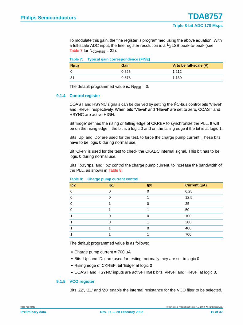
The default programmed value is as follows:
• NCOARSE = 32
• Gain = 0.825
• Vi to be full-scale = 1.212.
Table 5: Coding
Programmed code Clamp code ADC output
0 −63.5
underflow1 −63
2 −62.5
... ...
127 0 0
... ... ...
254 63.5 63 or 64
255 64 64
256 120 120
... ... ...
287 136 136
Table 6: Typical gain correspondence (COARSE)
NCOARSE Gain Vi to be full-scale (V)
32 0.825 1.212
99 2.5 0.4
GAINNCOARSE 1+
Vref 1NFINE
32 16×------------------– ⋅
------------------------------------------------
116------×
NCOARSE 1+
Vref . 512 NFINE–( )------------------------------------------------ 32×= =
Preliminary data Rev. 07 — 28 February 2002 18 of 37
9397 750 09457 © Koninklijke Philips Electronics N.V. 2002. All rights reserved.
Philips Semiconductors TDA8757Triple 8-bit ADC 170 Msps
To modulate this gain, the fine register is programmed using the above equation. Witha full-scale ADC input, the fine register resolution is a 1⁄2 LSB peak-to-peak (seeTable 7 for NCOARSE = 32).
The default programmed value is: NFINE = 0.
9.1.4 Control register
COAST and HSYNC signals can be derived by setting the I2C-bus control bits ‘Vlevel’and ‘Hlevel’ respectively. When bits ‘Vlevel’ and ‘Hlevel’ are set to zero, COAST andHSYNC are active HIGH.
Bit ‘Edge’ defines the rising or falling edge of CKREF to synchronize the PLL. It willbe on the rising edge if the bit is a logic 0 and on the falling edge if the bit is at logic 1.
Bits ‘Up’ and ‘Do’ are used for the test, to force the charge pump current. These bitshave to be logic 0 during normal use.
Bit ‘Cken’ is used for the test to check the CKADC internal signal. This bit has to belogic 0 during normal use.
Bits ‘Ip0’, ‘Ip1’ and ‘Ip2’ control the charge pump current, to increase the bandwidth ofthe PLL, as shown in Table 8.
The default programmed value is as follows:
• Charge pump current = 700 µA
• Bits ‘Up’ and ‘Do’ are used for testing, normally they are set to logic 0
• Rising edge of CKREF: bit ‘Edge’ at logic 0
• COAST and HSYNC inputs are active HIGH: bits ‘Vlevel’ and ‘Hlevel’ at logic 0.
9.1.5 VCO register
Bits ‘Z2’, ‘Z1’ and ‘Z0’ enable the internal resistance for the VCO filter to be selected.
Table 7: Typical gain correspondence (FINE)
NFINE Gain Vi to be full-scale (V)
0 0.825 1.212
31 0.878 1.139
Table 8: Charge pump current control
Ip2 Ip1 Ip0 Current ( µA)
0 0 0 6.25
0 0 1 12.5
0 1 0 25
0 1 1 50
1 0 0 100
1 0 1 200
1 1 0 400
1 1 1 700
Preliminary data Rev. 07 — 28 February 2002 19 of 37
9397 750 09457 © Koninklijke Philips Electronics N.V. 2002. All rights reserved.
Philips Semiconductors TDA8757Triple 8-bit ADC 170 Msps
Bits ‘Vco1’ and ‘Vco0’ control the VCO gain.
The default programmed value is as follows:
• Internal resistance = 2.25 kΩ
• VCO gain = 70 MHz/V.
9.1.6 Divider register
This register controls the PLL frequency. Bits ‘Di8’ to ‘Di0’ are the LSB bits. Thedefault programmed value is 0110 1001 1000 = 1688.
The MSB bits (‘Di11’, ‘Di10’ and ‘Di9’) and the LSB bit ‘Di0’ have to be programmedbefore bits ‘Di8’ to ‘Di1’ in order to have the required divider ratio. Bit ‘Di0’ is used forthe parity divider number (Di0 = 0: even number; Di0 = 1: odd number). It should benoted that if the I2C-bus programming is done in mode 1 and the bit ‘Di0’ has to betoggled, then the registers have to be loaded twice to update the divider ratio.
9.1.7 Phase register
Bit ‘Ckext’ is logic 0 when the PLL clock is used, and logic 1 when the external clockis used.
Bit ‘Ckrs’ is logic 1 when the synchronization is done with CKREF (see Figure 3).
Bits ‘P4’ to ‘P0’ are used to program the phase shift for the clock pixel.
Table 9: VCO register bits
Z2 Z1 Z0 Resistance (k Ω)
0 0 0 high-impedance
0 0 1 9
0 1 0 6.4
0 1 1 4.5
1 0 0 3.2
1 0 1 2.25
1 1 0 1.6
1 1 1 1.1
Table 10: VCO gain control
Vco1 Vco0 VCO gain (MHz/V) Pixel clockfrequency range(MHz)
0 0 12 10 to 20
0 1 20 20 to 40
1 0 40 40 to 85
1 1 70 85 to 170
Preliminary data Rev. 07 — 28 February 2002 20 of 37
9397 750 09457 © Koninklijke Philips Electronics N.V. 2002. All rights reserved.
Philips Semiconductors TDA8757Triple 8-bit ADC 170 Msps
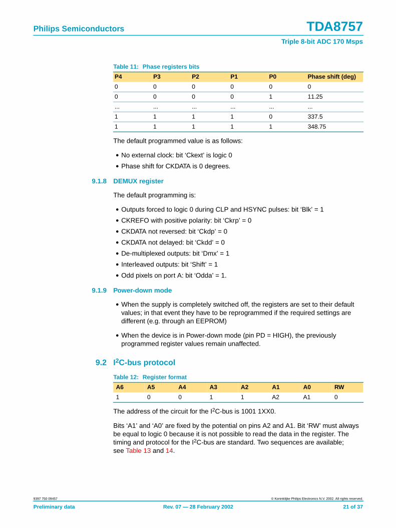
The default programmed value is as follows:
• No external clock: bit ‘Ckext’ is logic 0
• Phase shift for CKDATA is 0 degrees.
9.1.8 DEMUX register
The default programming is:
• Outputs forced to logic 0 during CLP and HSYNC pulses: bit ‘Blk’ = 1
• CKREFO with positive polarity: bit ‘Ckrp’ = 0
• CKDATA not reversed: bit ‘Ckdp’ = 0
• CKDATA not delayed: bit ‘Ckdd’ = 0
• De-multiplexed outputs: bit ‘Dmx’ = 1
• Interleaved outputs: bit ‘Shift’ = 1
• Odd pixels on port A: bit ‘Odda’ = 1.
9.1.9 Power-down mode
• When the supply is completely switched off, the registers are set to their defaultvalues; in that event they have to be reprogrammed if the required settings aredifferent (e.g. through an EEPROM)
• When the device is in Power-down mode (pin PD = HIGH), the previouslyprogrammed register values remain unaffected.
9.2 I2C-bus protocol
The address of the circuit for the I2C-bus is 1001 1XX0.
Bits ‘A1’ and ‘A0’ are fixed by the potential on pins A2 and A1. Bit ‘RW’ must alwaysbe equal to logic 0 because it is not possible to read the data in the register. Thetiming and protocol for the I2C-bus are standard. Two sequences are available;see Table 13 and 14.
Table 11: Phase registers bits
P4 P3 P2 P1 P0 Phase shift (deg)
0 0 0 0 0 0
0 0 0 0 1 11.25
... ... ... ... ... ...
1 1 1 1 0 337.5
1 1 1 1 1 348.75
Table 12: Register format
A6 A5 A4 A3 A2 A1 A0 RW
1 0 0 1 1 A2 A1 0
Preliminary data Rev. 07 — 28 February 2002 21 of 37
9397 750 09457 © Koninklijke Philips Electronics N.V. 2002. All rights reserved.
Philips Semiconductors TDA8757Triple 8-bit ADC 170 Msps
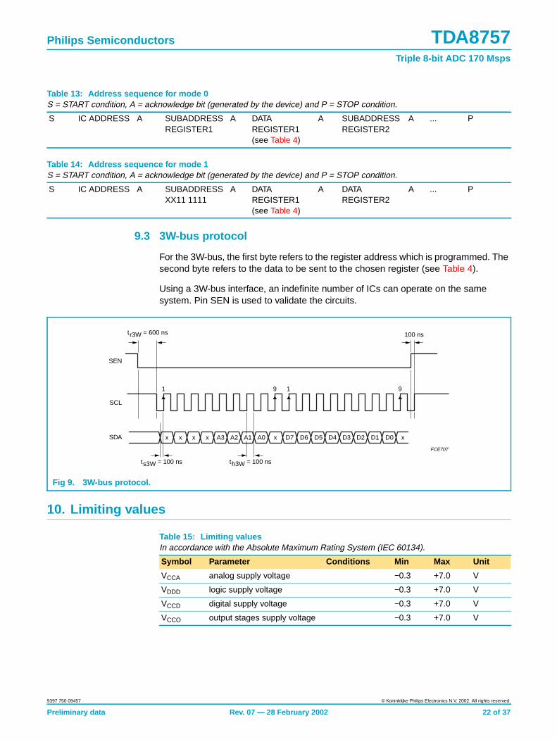
9.3 3W-bus protocol
For the 3W-bus, the first byte refers to the register address which is programmed. Thesecond byte refers to the data to be sent to the chosen register (see Table 4).
Using a 3W-bus interface, an indefinite number of ICs can operate on the samesystem. Pin SEN is used to validate the circuits.
10. Limiting values
Table 13: Address sequence for mode 0S = START condition, A = acknowledge bit (generated by the device) and P = STOP condition.
S IC ADDRESS A SUBADDRESSREGISTER1
A DATAREGISTER1(see Table 4)
A SUBADDRESSREGISTER2
A ... P
Table 14: Address sequence for mode 1S = START condition, A = acknowledge bit (generated by the device) and P = STOP condition.
S IC ADDRESS A SUBADDRESSXX11 1111
A DATAREGISTER1(see Table 4)
A DATAREGISTER2
A ... P
Fig 9. 3W-bus protocol.
FCE707
1
SEN
SCL
SDA
tr3W = 600 ns
ts3W = 100 ns th3W = 100 ns
9
x x x x x xA3 A2 A1 A0 D7 D6 D5 D4 D3 D2 D1 D0
1 9
100 ns
Table 15: Limiting valuesIn accordance with the Absolute Maximum Rating System (IEC 60134).
Symbol Parameter Conditions Min Max Unit
VCCA analog supply voltage −0.3 +7.0 V
VDDD logic supply voltage −0.3 +7.0 V
VCCD digital supply voltage −0.3 +7.0 V
VCCO output stages supply voltage −0.3 +7.0 V
Preliminary data Rev. 07 — 28 February 2002 22 of 37
9397 750 09457 © Koninklijke Philips Electronics N.V. 2002. All rights reserved.
Philips Semiconductors TDA8757Triple 8-bit ADC 170 Msps
11. Thermal characteristics
12. Characteristics
∆VCC supply voltage differences
VCCA − VCCD −1.0 +1.0 V
VCCO − VCCD −1.0 +1.0 V
VCCO − VDDD −1.0 +1.0 V
VCCA − VDDD −1.0 +1.0 V
VCCD − VDDD −1.0 +1.0 V
VCCA − VCCO −1.0 +1.0 V
Vi(RGB) RGB input voltage range referencedto AGND
−0.3 +7.0 V
Io output current − 10 mA
Tstg storage temperature −55 +150 °C
Tamb ambient temperature 0 70 °C
Tj junction temperature − 150 °C
Table 15: Limiting values …continuedIn accordance with the Absolute Maximum Rating System (IEC 60134).
Symbol Parameter Conditions Min Max Unit
Table 16: Typical thermal characteristics
Symbol Parameter Conditions Value Unit
Rth(j-a) thermal resistance from junction toambient
in free air 30 K/W
Table 17: CharacteristicsVCCA = 4.75 V to 5.25 V (referenced to AGND); VCCD = 4.75 V to 5.25 V (referenced to DGND); VDDD = 4.75 V to 5.25 V(referenced to VSSD); VCCO = 4.75 V to 5.25 V (referenced to OGND); AGND, DGND, OGND and VSS connected together;Tamb = 0 to 70 °C; typical values measured at VCCA = VDDD = VCCD = VCCO = 5 V and Tamb = 25 °C; unless otherwisespecified.
Symbol Parameter Conditions Min Typ Max Unit
Supplies
VCCA(PLL),VCCA(R),VCCA(G),VCCA(B)
analog supply voltage for PLL andthe RGB channels
4.75 5.0 5.25 V
VDDD logic supply voltage for I2C-busand 3W-bus
4.75 5.0 5.25 V
VCCD digital supply voltage 4.75 5.0 5.25 V
VCCO(PLL),VCCO(R),VCCO(G),VCCO(B)
output stages supply voltage forPLL and the RGB channels
4.75 5.0 5.25 V
ICCA(PLL) analog PLL supply current − 34 − mA
Preliminary data Rev. 07 — 28 February 2002 23 of 37
9397 750 09457 © Koninklijke Philips Electronics N.V. 2002. All rights reserved.
Philips Semiconductors TDA8757Triple 8-bit ADC 170 Msps
ICCA(R),ICCA(G),ICCA(B)
analog supply current for theRGB channels
− 135 − mA
IDDD logic supply current for I2C-busand 3W-bus
− 1 − mA
ICCD digital supply current − 95 − mA
ICCO(R),ICCO(G),ICCO(B),ICCO(PLL)
output stages supply current forthe RGB channels and PLL
sinusoidal input − 80 − mA
∆VCC supply voltage difference
VCCA − VCCD −0.25 − +0.25 V
VCCO − VCCD −0.25 − +0.25 V
VCCO − VDDD −0.25 − +0.25 V
VCCA − VDDD −0.25 − +0.25 V
VCCD − VDDD −0.25 − +0.25 V
VCCA − VCCO −0.25 − +0.25 V
Ptot total power dissipation sinusoidal input − 1.5 − W
Ppd power dissipation in Power-downmode
− 55 − mW
R, G and B amplifiers
B bandwidth −3 dB; Tamb = 25 °C 250 − − MHz
tset(ADC+AGC) settling time of the blockADC + AGC
full-scale (black to white)transition; input signalsettling time <1 ns; settlingto within 2 LSB
− 4 − ns
GCOARSE coarse gain range minimum coarse gain;code = 32
− −1.67 − dB
maximum coarse gain;code = 99
− 8 − dB
GFINE fine gain correction range minimum fine inputcode = 0
− 0 − dB
maximum fine inputcode = 31
− −0.5 − dB
∆Gamp/∆T amplifier gain stability variationwith temperature
Vref with 100 ppm/°Cmaximum variation
− 325 − ppm/°C
IGC gain current − ±20 − µA
tstab amplifier gain adjustment speedfrom minimum to maximum gain
HSYNC active; capacitorson pins 8, 16 and 24 are22 nF
− 25 − mdB/µs
Vref amplifier reference voltage − 2.5 − V
Table 17: Characteristics …continuedVCCA = 4.75 V to 5.25 V (referenced to AGND); VCCD = 4.75 V to 5.25 V (referenced to DGND); VDDD = 4.75 V to 5.25 V(referenced to VSSD); VCCO = 4.75 V to 5.25 V (referenced to OGND); AGND, DGND, OGND and VSS connected together;Tamb = 0 to 70 °C; typical values measured at VCCA = VDDD = VCCD = VCCO = 5 V and Tamb = 25 °C; unless otherwisespecified.
Symbol Parameter Conditions Min Typ Max Unit
Preliminary data Rev. 07 — 28 February 2002 24 of 37
9397 750 09457 © Koninklijke Philips Electronics N.V. 2002. All rights reserved.
Philips Semiconductors TDA8757Triple 8-bit ADC 170 Msps
Iref amplifier reference voltagecurrent
− 50 − µA
Vi(p-p) input voltage(peak-to-peak value)
corresponding to full-scaleinput at high gain
− 0.4 − V
corresponding to full-scaleoutput at low gain
− − 1.212 V
Ci input capacitance − 10 − pF
GE(rms) channel-to-channel gainmatching (RMS value)
maximum coarse gain;Tamb = 25 °C
− 1 − %
minimum coarse gain;Tamb = 25 °C
− 5 − %
Clamps
PCLP precision maximum black level noiseon RGB channels = 10 mV;Tamb = 25 °C
− 0.5 − LSB
tW(CLP) clamp pulse width 500 − 2000 ns
CLPE channel-to-channel clampmatching
− 0.5 − LSB
Aoff code clamp reference clamp register inputcode = 0
− −63.5 − LSB
clamp register inputcode = 255
− +64 − LSB
clamp register inputcode = 256
− +120 − LSB
clamp register inputcode = 287
− +135.5 − LSB
Phase-locked loop (PLL)
jPLL(max)(p-p) long term PLL phase jitter(peak-to-peak value)
fclk = 170 MHz − 360 − ps
DR divider ratio 100 − 4095 −
fref reference clock frequency 15 − 150 kHz
fPLL output clock frequency 10 − 170 MHz
∆Φstep phase drift [1] standard at 160 Msps − − 2 step
Φstep phase shift step Tamb = 25 °C − 11.25 − deg
ADCs
fs maximum sampling frequency 170 − − MHz
INL DC integral non-linearity from IC analog input todigital output; sinusoidalinput; fclk = 170 MHz
− ±0.5 ±1.5 LSB
DNL DC differential non-linearity from IC analog input todigital output; sinusoidalinput; fclk = 170 MHz
− ±0.4 ±1 LSB
Table 17: Characteristics …continuedVCCA = 4.75 V to 5.25 V (referenced to AGND); VCCD = 4.75 V to 5.25 V (referenced to DGND); VDDD = 4.75 V to 5.25 V(referenced to VSSD); VCCO = 4.75 V to 5.25 V (referenced to OGND); AGND, DGND, OGND and VSS connected together;Tamb = 0 to 70 °C; typical values measured at VCCA = VDDD = VCCD = VCCO = 5 V and Tamb = 25 °C; unless otherwisespecified.
Symbol Parameter Conditions Min Typ Max Unit
Preliminary data Rev. 07 — 28 February 2002 25 of 37
9397 750 09457 © Koninklijke Philips Electronics N.V. 2002. All rights reserved.
Philips Semiconductors TDA8757Triple 8-bit ADC 170 Msps
ENOB [2] effective number of bits − 7.4 − bits
Signal-to-noise ratio
S/N signal-to-noise ratio fclk = 170 MHz − 46 − dB
Spurious free dynamic range
SFDR spurious free dynamic range fclk = 170 MHz − 57 − dB
Clock timing output (CKDATA)
ηext ADC clock duty factor 45 50 55 %
fclk(max) maximum clock frequency − − 170 MHz
Clock timing input (CKEXT)
fclk(max) maximum clock frequency − − 170 MHz
tCPH clock pulse width HIGH 2.5 − − ns
tCPL clock pulse width LOW 2.5 − − ns
Data timing [3]
td(s) sampling delay time all times referenced to 50% ofthe rising edge of CKDATA; seeFigure 10
− −7.5 − ns
tsu(d)(o) output data set-up time − −7 − ns
th(o) output hold time − 1 − ns
3-state output delay time
tdZH output enable HIGH − 15 − ns
tdZL output enable LOW − 18 − ns
tdHZ output disable HIGH − 13 − ns
tdLZ output disable LOW − 10 − ns
Data and sync outputs
VOL LOW-level output voltage Io = 1 mA − − 0.4 V
VOH HIGH-level output voltage Io = 1 mA 2.4 − − V
IOL LOW-level output current VOL = 0.2 V − 0.2 − mA
IOH HIGH-level output current VOH = 3.4 V − 0.3 − mA
CL load capacitance − 10 − pF
TTL digital inputs (CKREF, COAST, INV, HSYNC, CLP, PD, DIS, I 2C/3W, OE, CKEXT)
VIL LOW-level input voltage − − 0.8 V
VIH HIGH-level input voltage 2.0 − − V
IIL LOW-level input current − 400 − µA
IIH HIGH-level input current − 35 − µA
Zi input impedance − tbf − kΩ
Ci input capacitance − tbf − pF
Sync on green input
Vsync(G) sync on green pulse amplitude [4] Slevel = 0; see Figure 5 300 − 600 mV
Slevel = 1; see Figure 5 150 − 300 mV
Table 17: Characteristics …continuedVCCA = 4.75 V to 5.25 V (referenced to AGND); VCCD = 4.75 V to 5.25 V (referenced to DGND); VDDD = 4.75 V to 5.25 V(referenced to VSSD); VCCO = 4.75 V to 5.25 V (referenced to OGND); AGND, DGND, OGND and VSS connected together;Tamb = 0 to 70 °C; typical values measured at VCCA = VDDD = VCCD = VCCO = 5 V and Tamb = 25 °C; unless otherwisespecified.
Symbol Parameter Conditions Min Typ Max Unit
Preliminary data Rev. 07 — 28 February 2002 26 of 37
9397 750 09457 © Koninklijke Philips Electronics N.V. 2002. All rights reserved.
Philips Semiconductors TDA8757Triple 8-bit ADC 170 Msps
[1] From 25 to 70 °C, the edge of the clock CKDATA has a shift of 1 phase compared to CKREF.
[2] Effective bits are obtained from a Fast Fourier Transform (FFT) treatment taking 8000 acquisition points per equivalent fundamentalperiod. The calculation takes into account all harmonics and noise up to half clock frequency (NYQUIST frequency).Conversion-to-noise ratio: S/N = EB × 6.02 + 1.76 dB.
[3] Output data acquisition: the output data is available after the maximum sampling delay time td(s). All the timings are given for a 10 pFcapacitive load.
[4] Pulse relative to the blank level.
[5] The I2C-bus timings are given for use of the bus at a frequency of 100 kbit/s (100 kHz). This bus could be used at a frequency of400 kbit/s (400 kHz).
3W-bus
trst reset time of the chip before3-wire communication
− 600 − ns
tsu data set-up time for 3-wirecommunication
− 100 − ns
th data hold time for 3-wirecommunication
− 100 − ns
I2C-bus [5]
VIL LOW-level input voltage for SCL and SDA − − 0.3VDD V
VIH HIGH-level input voltage for SCL and SDA;VPU = 5 V
3 − − V
for SCL and SDA;VPU = 3 V
0.7VDD − −
fSCL clock frequency 0 − 100 kHz
tBUF time the bus must be free beforenew transmission can start
4.7 − − µs
tHD;STA start condition hold time 4.0 − − µs
tSU;STA start condition set-up time repeated start 4.7 − − µs
tLOW LOW-level clock period 4.7 − − µs
tHIGH HIGH-level clock period 4.0 − − µs
tSU;DAT data set-up time 250 − − ns
tHD;DAT data hold time 0 − − ns
tr SDA and SCL rise time fSCL = 100 kHz − − 1.0 µs
tf SDA and SCL fall time fSCL = 100 kHz − − 300 ns
tSU;STO stop condition set-up time 4.0 − − µs
Cb bus line capacitive loading − − 400 pF
Table 17: Characteristics …continuedVCCA = 4.75 V to 5.25 V (referenced to AGND); VCCD = 4.75 V to 5.25 V (referenced to DGND); VDDD = 4.75 V to 5.25 V(referenced to VSSD); VCCO = 4.75 V to 5.25 V (referenced to OGND); AGND, DGND, OGND and VSS connected together;Tamb = 0 to 70 °C; typical values measured at VCCA = VDDD = VCCD = VCCO = 5 V and Tamb = 25 °C; unless otherwisespecified.
Symbol Parameter Conditions Min Typ Max Unit
Preliminary data Rev. 07 — 28 February 2002 27 of 37
9397 750 09457 © Koninklijke Philips Electronics N.V. 2002. All rights reserved.
Philips Semiconductors TDA8757Triple 8-bit ADC 170 Msps
[1] PLL long-term time jitter is measured at the end of the video line, where it is at its maximum.
Table 18: Examples of PLL settings and performanceVCCA = VDDD = VCCD = VCCO = 5 V; Tamb = 25 °C.
Video standards fref(kHz)
fclk(MHz)
N KO(MHz/V)
CZ(nF)
CP(nF)
IP(µA)
Z(kΩ)
Long-term time jitter [1]
RMS-value(ps)
peak-to-peakvalue (ps)
VGA: 640 × 480 31.469 25.175 800 20 68 0.15 200 4.5 242 1452
VESA: 800 × 600(SVGA 72 Hz)
48.08 50 1040 40 68 0.15 700 1.6 225 1350
VESA: 1024 × 768(XGA 75 Hz)
60.02 78.75 1312 40 68 0.15 400 4.5 120 720
VESA: 1280 × 1024(SXGA 60 Hz)
63.98 108 1688 70 68 0.15 400 3.2 98 588
VESA: 1280 × 1024(SXGA 75 Hz)
80.00 135 1688 70 68 0.15 400 4.5 70 420
VESA: 1600 × 1200(UXGA 60 Hz)
75.00 162 2160 70 68 0.15 400 4.5 65 390
Fig 10. Data timing; Dmx = 0; n = even pixel.
CKDATA 50%
tCPLtCPH
DATA
2.4 V
0.4 V
n
In−1 In+1In
Sample n
Sample n+1
Sample n+3
Sample n+2
td(s)
tsu(d)(o)
th(o)
Vin
FCE700
Fig 11. Timing diagram; single port mode; Dmx = 0, Ckdd = 0, Ckdp = 0; n = even pixel.
CKDATA
OUT A
n n+1 n+2 n+3 n+4 n+5 n+6 n+7RGBIN
CKADC
n-1 n n+1 n+2 n+3 n+4n-2 n+5
FCE701
Preliminary data Rev. 07 — 28 February 2002 28 of 37
9397 750 09457 © Koninklijke Philips Electronics N.V. 2002. All rights reserved.
Philips Semiconductors TDA8757Triple 8-bit ADC 170 Msps
Fig 12. Timing diagram; dual port mode, interleaved outputs, even pixels on port A; Dmx = 1, Shift = 1, Odda = 0,Ckdd = 0, Ckdp = 0; n = even pixel.
CKADC
CKDATA
n n+1 n+2 n+3 n+4 n+5 n+6 n+7RGBIN
OUT A
OUT B
n-2 n n+2 n+4
n-1 n+1 n+3
FCE702
Fig 13. Timing diagram; dual port mode, interleaved outputs, odd pixels on port A; Dmx = 1, Shift = 1, Odda = 1,Ckdd = 0, Ckdp = 0; n = even pixel.
n n+1 n+2 n+3 n+4 n+5 n+6 n+7RGBIN
CKADC
CKDATA
OUT B
OUT A n+3
n+4
FCE703
n+1
n+2n
n-1
n-2
Preliminary data Rev. 07 — 28 February 2002 29 of 37
9397 750 09457 © Koninklijke Philips Electronics N.V. 2002. All rights reserved.
Philips Semiconductors TDA8757Triple 8-bit ADC 170 Msps
Fig 14. Timing diagram; dual port mode, synchronized outputs, even pixels on port A; Dmx = 1, Shift = 0,Odda = 0, Ckdd = 0, Ckdp = 0; n = even pixel.
n n+1 n+2 n+3 n+4 n+5 n+6 n+7RGBIN
CKADC
OUT B
OUT A
CKDATA
n-2 n n+2n-4
n-1 n+1 n+3n-3
FCE704
Fig 15. Timing diagram; dual port mode, synchronized outputs, odd pixels on port A; Dmx = 1, Shift = 0, Odda = 1,Ckdd = 0, Ckdp = 0; n = even pixel.
RGBIN
CKADC
OUT A
OUT B
CKDATA
FCE705
n+2
n+5
n+4
n+1
n
n+3
n+1n n+2 n+6n+3 n+4 n+5 n+7
n-1
n-2
Preliminary data Rev. 07 — 28 February 2002 30 of 37
9397 750 09457 © Koninklijke Philips Electronics N.V. 2002. All rights reserved.
Philips Semiconductors TDA8757Triple 8-bit ADC 170 Msps
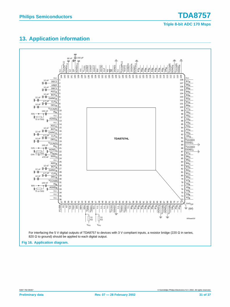
13. Application information
For interfacing the 5 V digital outputs of TDA8757 to devices with 3 V compliant inputs, a resistor bridge (220 Ω in series,820 Ω to ground) should be applied to each digital output.
Fig 16. Application diagram.
005aaa010
TDA8757HL
1
2
3
4
5
6
7
8
9
10
11
12
13
14
15
16
17
18
19
20
21
22
23
24
25
26
27
28
29
30
31
32
33
34
35
36
DEC2
VREFDEC1AGCRBOTR
GAINCRCLPRDECR
INR
AGCGBOTG
GAINCGCLPGDECG
INGAGNDG
AGCBBOTB
GAINCBCLPBDECB
INB
B7RB6RB5RB4RB3RB2RB1RB0RA7GA6GA5GA4GA3GA2GA1GA0GORG
B7GB6GB5GB4GB3GB2GB1GB0GA7BA6BA5BA4BA3BA2B
108
107
106
105
104
103
102
101
100
99
98
97
96
95
94
93
92
91
90
89
88
87
86
85
84
83
82
81
80
79
78
77
76
75
74
73
37 38 39 40 41 42 43 44 45 46 47 48 49 50 51 52 53 54 55 56 57 58 59 60 61 62 63 64 65 66 67 68 69 70 71 72
144
143
142
141
140
139
138
137
136
135
134
133
132
131
130
129
128
127
126
125
124
123
122
121
120
119
118
117
116
115
114
113
112
111
110
109
A1
A2
TC
K
TD
O
DIS
SE
N
SD
A
SC
L
DG
ND
2
B0 B
B1 B
B2 B
B3 B
B4 B
B5 B
B6 B
B7 B
OR
BA
0 BA
1 B
CZ
CP
CK
RE
F
CO
AS
T
CK
EX
T
INV
HS
YN
C
CLP
PD
OE
DG
ND
1
TE
ST
O
CK
RE
FO
CK
DA
TA
A7 R
A6 R
A5 R
A4 R
A3 R
A2 R
A1 R
A0 R
OR
R
10kΩ
75 or 50Ω
10kΩ
150 pF68 nF
10 nF
10 nF
10 nF
10 nF
4.7 nF
4.7 nF
100 nF
22 nF
22 nF
10 nF
10 nF
4.7 nF
22 nF
10 nF
10 nF
RIN
75 or 50Ω
100 nFGIN
75 or 50Ω
100 nFBIN
n.c.
VCCA(R)
n.c.
AGNDRn.c.
INSOGSOGO
n.c.
VCCA(B)
AGNDBn.c.
n.c.
n.c.
VCCA(G)
I2C
/3W
VD
DD
VS
SD
1
n.c.
n.c.
n.c.
n.c.
VC
CD
2
n.c.
VS
SD
2V
SS
D3
n.c.
OG
ND
OG
ND
VC
CO
(B)
VC
CO
(B)B B
VPU VPU
n.c.
VCCO(G)OGND
VCCO(G)OGND
G
G
n.c.
VC
CA
(PLL
)A
GN
D
AG
ND
n.c.
VC
CD
1
n.c.
VC
CO
(PLL
)
OG
ND
VC
CO
(R)
OG
ND
VC
CO
(R)
OG
NDP
LL RRPLL
PLL
GNDDP
470 nFGIN
(tbf)
Preliminary data Rev. 07 — 28 February 2002 31 of 37
9397 750 09457 © Koninklijke Philips Electronics N.V. 2002. All rights reserved.
Philips Semiconductors TDA8757Triple 8-bit ADC 170 Msps
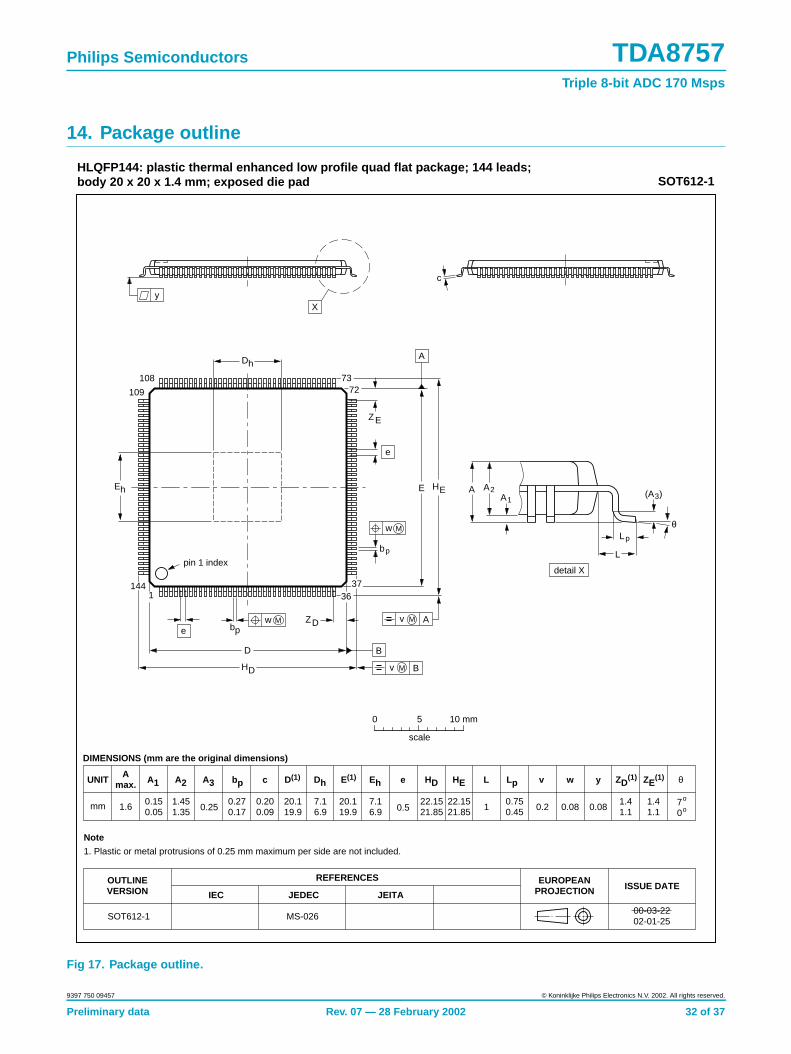
14. Package outline
Fig 17. Package outline.
UNIT A1 A2 A3 bp c e HEHD L Lp ZE(1)ZD
(1)ywv θ
REFERENCESOUTLINEVERSION
EUROPEANPROJECTION ISSUE DATE
IEC JEDEC JEITA
mm 0.150.05
1.451.35 0.25
0.270.17
0.200.09
20.119.9 0.5
22.1521.85
1.41.1
70
o
o0.080.2 0.081
DIMENSIONS (mm are the original dimensions)
Note
1. Plastic or metal protrusions of 0.25 mm maximum per side are not included.
0.750.45
SOT612-1 MS-02600-03-2202-01-25
D(1) E(1)
20.119.9
Dh
7.16.9
Eh
7.16.9
22.1521.85
1.41.1
0 5 10 mm
scale
bpe
θ
EA1
A
Lp
detail X
L
(A )3
B
c
bp
EH A2
DH v M B
D
ZD
A
ZE
e
v M A
Xy
w M
w M
Amax.
1.6
HLQFP144: plastic thermal enhanced low profile quad flat package; 144 leads;body 20 x 20 x 1.4 mm; exposed die pad SOT612-1
108
109
pin 1 index
Eh
Dh
7372
371
14436
Preliminary data Rev. 07 — 28 February 2002 32 of 37
9397 750 09457 © Koninklijke Philips Electronics N.V. 2002. All rights reserved.
Philips Semiconductors TDA8757Triple 8-bit ADC 170 Msps
15. Handling information
Inputs and outputs are protected against electrostatic discharge in normal handling.However, to be completely safe, it is desirable to take normal precautions appropriateto handling integrated circuits.
16. Soldering
16.1 Introduction to soldering surface mount packages
This text gives a very brief insight to a complex technology. A more in-depth accountof soldering ICs can be found in our Data Handbook IC26; Integrated CircuitPackages (document order number 9398 652 90011).
There is no soldering method that is ideal for all surface mount IC packages. Wavesoldering can still be used for certain surface mount ICs, but it is not suitable for finepitch SMDs. In these situations reflow soldering is recommended.
16.2 Reflow soldering
Reflow soldering requires solder paste (a suspension of fine solder particles, flux andbinding agent) to be applied to the printed-circuit board by screen printing, stencillingor pressure-syringe dispensing before package placement.
Several methods exist for reflowing; for example, convection or convection/infraredheating in a conveyor type oven. Throughput times (preheating, soldering andcooling) vary between 100 and 200 seconds depending on heating method.
Typical reflow peak temperatures range from 215 to 250 °C. The top-surfacetemperature of the packages should preferable be kept below 220 °C for thick/largepackages, and below 235 °C small/thin packages.
16.3 Wave soldering
Conventional single wave soldering is not recommended for surface mount devices(SMDs) or printed-circuit boards with a high component density, as solder bridgingand non-wetting can present major problems.
To overcome these problems the double-wave soldering method was specificallydeveloped.
If wave soldering is used the following conditions must be observed for optimalresults:
• Use a double-wave soldering method comprising a turbulent wave with highupward pressure followed by a smooth laminar wave.
• For packages with leads on two sides and a pitch (e):
– larger than or equal to 1.27 mm, the footprint longitudinal axis is preferred to beparallel to the transport direction of the printed-circuit board;
– smaller than 1.27 mm, the footprint longitudinal axis must be parallel to thetransport direction of the printed-circuit board.
Preliminary data Rev. 07 — 28 February 2002 33 of 37
9397 750 09457 © Koninklijke Philips Electronics N.V. 2002. All rights reserved.
Philips Semiconductors TDA8757Triple 8-bit ADC 170 Msps
The footprint must incorporate solder thieves at the downstream end.
• For packages with leads on four sides, the footprint must be placed at a 45° angleto the transport direction of the printed-circuit board. The footprint mustincorporate solder thieves downstream and at the side corners.
During placement and before soldering, the package must be fixed with a droplet ofadhesive. The adhesive can be applied by screen printing, pin transfer or syringedispensing. The package can be soldered after the adhesive is cured.
Typical dwell time is 4 seconds at 250 °C. A mildly-activated flux will eliminate theneed for removal of corrosive residues in most applications.
16.4 Manual soldering
Fix the component by first soldering two diagonally-opposite end leads. Use a lowvoltage (24 V or less) soldering iron applied to the flat part of the lead. Contact timemust be limited to 10 seconds at up to 300 °C.
When using a dedicated tool, all other leads can be soldered in one operation within2 to 5 seconds between 270 and 320 °C.
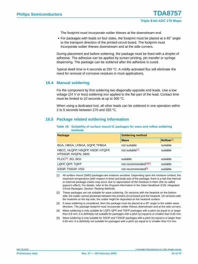
16.5 Package related soldering information
[1] All surface mount (SMD) packages are moisture sensitive. Depending upon the moisture content, themaximum temperature (with respect to time) and body size of the package, there is a risk that internalor external package cracks may occur due to vaporization of the moisture in them (the so calledpopcorn effect). For details, refer to the Drypack information in the Data Handbook IC26; IntegratedCircuit Packages; Section: Packing Methods.
[2] These packages are not suitable for wave soldering. On versions with the heatsink on the bottomside, the solder cannot penetrate between the printed-circuit board and the heatsink. On versions withthe heatsink on the top side, the solder might be deposited on the heatsink surface.
[3] If wave soldering is considered, then the package must be placed at a 45° angle to the solder wavedirection. The package footprint must incorporate solder thieves downstream and at the side corners.
[4] Wave soldering is only suitable for LQFP, QFP and TQFP packages with a pitch (e) equal to or largerthan 0.8 mm; it is definitely not suitable for packages with a pitch (e) equal to or smaller than 0.65 mm.
[5] Wave soldering is only suitable for SSOP and TSSOP packages with a pitch (e) equal to or larger than0.65 mm; it is definitely not suitable for packages with a pitch (e) equal to or smaller than 0.5 mm.
Table 19: Suitability of surface mount IC packages for wave and reflow solderingmethods
Package Soldering method
Wave Reflow [1]
BGA, HBGA, LFBGA, SQFP, TFBGA not suitable suitable
HBCC, HLQFP, HSQFP, HSOP, HTQFP,HTSSOP, HVQFN, SMS
not suitable[2] suitable
PLCC[3], SO, SOJ suitable suitable
LQFP, QFP, TQFP not recommended[3][4] suitable
SSOP, TSSOP, VSO not recommended[5] suitable
Preliminary data Rev. 07 — 28 February 2002 34 of 37
9397 750 09457 © Koninklijke Philips Electronics N.V. 2002. All rights reserved.
Philips Semiconductors TDA8757Triple 8-bit ADC 170 Msps
17. Revision history
Table 20: Revision history
Rev Date CPCN Description
07 20020228 - Preliminary data (9397 750 09457); seventh version
Preliminary data Rev. 07 — 28 February 2002 35 of 37
9397 750 09457 © Koninklijke Philips Electronics N.V. 2002. All rights reserved.
Philips Semiconductors TDA8757Triple 8-bit ADC 170 Msps
18. Data sheet status
[1] Please consult the most recently issued data sheet before initiating or completing a design.
[2] The product status of the device(s) described in this data sheet may have changed since this data sheet was published. The latest information is available on the Internet atURL http://www.semiconductors.philips.com.
19. Definitions
Short-form specification — The data in a short-form specification isextracted from a full data sheet with the same type number and title. Fordetailed information see the relevant data sheet or data handbook.
Limiting values definition — Limiting values given are in accordance withthe Absolute Maximum Rating System (IEC 60134). Stress above one ormore of the limiting values may cause permanent damage to the device.These are stress ratings only and operation of the device at these or at anyother conditions above those given in the Characteristics sections of thespecification is not implied. Exposure to limiting values for extended periodsmay affect device reliability.
Application information — Applications that are described herein for anyof these products are for illustrative purposes only. Philips Semiconductorsmake no representation or warranty that such applications will be suitable forthe specified use without further testing or modification.
20. Disclaimers
Life support — These products are not designed for use in life supportappliances, devices, or systems where malfunction of these products canreasonably be expected to result in personal injury. Philips Semiconductors
customers using or selling these products for use in such applications do soat their own risk and agree to fully indemnify Philips Semiconductors for anydamages resulting from such application.
Right to make changes — Philips Semiconductors reserves the right tomake changes, without notice, in the products, including circuits, standardcells, and/or software, described or contained herein in order to improvedesign and/or performance. Philips Semiconductors assumes noresponsibility or liability for the use of any of these products, conveys nolicence or title under any patent, copyright, or mask work right to theseproducts, and makes no representations or warranties that these products arefree from patent, copyright, or mask work right infringement, unless otherwisespecified.
21. Licenses
Data sheet status [1] Product status [2] Definition
Objective data Development This data sheet contains data from the objective specification for product development. Philips Semiconductorsreserves the right to change the specification in any manner without notice.
Preliminary data Qualification This data sheet contains data from the preliminary specification. Supplementary data will be published at alater date. Philips Semiconductors reserves the right to change the specification without notice, in order toimprove the design and supply the best possible product.
Product data Production This data sheet contains data from the product specification. Philips Semiconductors reserves the right tomake changes at any time in order to improve the design, manufacturing and supply. Changes will becommunicated according to the Customer Product/Process Change Notification (CPCN) procedureSNW-SQ-650A.
Purchase of Philips I 2C components
Purchase of Philips I2C components conveys a licenseunder the Philips’ I2C patent to use the components in theI2C system provided the system conforms to the I2Cspecification defined by Philips. This specification can beordered using the code 9398 393 40011.
9397 750 09457 © Koninklijke Philips Electronics N.V. 2002. All rights reserved.
Preliminary data Rev. 07 — 28 February 2002 36 of 37
Contact informationFor additional information, please visit http://www.semiconductors.philips.com .For sales office addresses, send e-mail to: [email protected] . Fax: +31 40 27 24825
© Koninklijke Philips Electronics N.V. 2002.Printed in The Netherlands
All rights are reserved. Reproduction in whole or in part is prohibited without the priorwritten consent of the copyright owner.
The information presented in this document does not form part of any quotation orcontract, is believed to be accurate and reliable and may be changed without notice. Noliability will be accepted by the publisher for any consequence of its use. Publicationthereof does not convey nor imply any license under patent- or other industrial orintellectual property rights.
Date of release: 28 February 2002 Document order number: 9397 750 09457
Contents
Philips Semiconductors TDA8757Triple 8-bit ADC 170 Msps
1 General description . . . . . . . . . . . . . . . . . . . . . . 22 Features . . . . . . . . . . . . . . . . . . . . . . . . . . . . . . . 23 Applications . . . . . . . . . . . . . . . . . . . . . . . . . . . . 24 Quick reference data . . . . . . . . . . . . . . . . . . . . . 35 Ordering information . . . . . . . . . . . . . . . . . . . . . 46 Block diagram . . . . . . . . . . . . . . . . . . . . . . . . . . 47 Pinning information . . . . . . . . . . . . . . . . . . . . . . 77.1 Pinning . . . . . . . . . . . . . . . . . . . . . . . . . . . . . . . 77.2 Pin description . . . . . . . . . . . . . . . . . . . . . . . . . 78 Functional description . . . . . . . . . . . . . . . . . . 118.1 Analog video inputs . . . . . . . . . . . . . . . . . . . . 118.2 Clamps . . . . . . . . . . . . . . . . . . . . . . . . . . . . . . 128.2.1 Variable gain amplifiers . . . . . . . . . . . . . . . . . 138.2.2 Important recommendations . . . . . . . . . . . . . . 138.2.3 ADCs . . . . . . . . . . . . . . . . . . . . . . . . . . . . . . . 148.2.4 Data outputs . . . . . . . . . . . . . . . . . . . . . . . . . . 148.2.5 PLL . . . . . . . . . . . . . . . . . . . . . . . . . . . . . . . . . 149 I2C-bus and 3W-bus interfaces . . . . . . . . . . . . 179.1 Register definitions . . . . . . . . . . . . . . . . . . . . . 179.1.1 Subaddress. . . . . . . . . . . . . . . . . . . . . . . . . . . 179.1.2 Offset register . . . . . . . . . . . . . . . . . . . . . . . . . 179.1.3 Coarse and Fine registers . . . . . . . . . . . . . . . 189.1.4 Control register . . . . . . . . . . . . . . . . . . . . . . . . 199.1.5 VCO register . . . . . . . . . . . . . . . . . . . . . . . . . . 199.1.6 Divider register . . . . . . . . . . . . . . . . . . . . . . . . 209.1.7 Phase register. . . . . . . . . . . . . . . . . . . . . . . . . 209.1.8 DEMUX register . . . . . . . . . . . . . . . . . . . . . . . 219.1.9 Power-down mode . . . . . . . . . . . . . . . . . . . . . 219.2 I2C-bus protocol . . . . . . . . . . . . . . . . . . . . . . . 219.3 3W-bus protocol . . . . . . . . . . . . . . . . . . . . . . . 2210 Limiting values . . . . . . . . . . . . . . . . . . . . . . . . . 2211 Thermal characteristics . . . . . . . . . . . . . . . . . . 2312 Characteristics . . . . . . . . . . . . . . . . . . . . . . . . . 2313 Application information . . . . . . . . . . . . . . . . . . 3114 Package outline . . . . . . . . . . . . . . . . . . . . . . . . 3215 Handling information . . . . . . . . . . . . . . . . . . . . 3316 Soldering . . . . . . . . . . . . . . . . . . . . . . . . . . . . . 3316.1 Introduction to soldering surface mount
packages . . . . . . . . . . . . . . . . . . . . . . . . . . . . 3316.2 Reflow soldering . . . . . . . . . . . . . . . . . . . . . . . 3316.3 Wave soldering . . . . . . . . . . . . . . . . . . . . . . . . 3316.4 Manual soldering . . . . . . . . . . . . . . . . . . . . . . 3416.5 Package related soldering information . . . . . . 3417 Revision history . . . . . . . . . . . . . . . . . . . . . . . . 3518 Data sheet status . . . . . . . . . . . . . . . . . . . . . . . 3619 Definitions . . . . . . . . . . . . . . . . . . . . . . . . . . . . 36
20 Disclaimers . . . . . . . . . . . . . . . . . . . . . . . . . . . 3621 Licenses . . . . . . . . . . . . . . . . . . . . . . . . . . . . . . 36
Related Documents