1 SLVA782 – June 2016 Submit Documentation Feedback Copyright © 2016, Texas Instruments Incorporated TPS65982 Designs for Supporting Voltages in USB-PD "Power Rules" NexFET is a trademark of Texas Instruments. USB Type-C is a registered trademark of Universal Serial Bus Consortium. Application Report SLVA782 – June 2016 TPS65982 Designs for Supporting Voltages in USB-PD "Power Rules" ABSTRACT The TPS65982 is a stand-alone USB Type-C ® and Power Delivery (PD) controller providing cable plug and orientation detection at the USB Type-C connector. The latest revision of the USB Power Delivery specification outlines a new set of “Power Rules” requiring the following voltages to be sourced by a compliant product: 5, 9, 15, and 20 Volts. Existing reference designs of the TPS65982 followed the “Power Profiles” put forth in the original USB PD specification. In USB PD releases up to Revision 2.0, Version 1.1 the required voltages were limited to 5, 12, and 20 Volts. In order to comply with the new standard and keep design effort simple, this application report outlines a few options for a new power circuit to meet the new USB PD “Power Rules”. Although more than one power circuit will work, the simplest and most cost- effective solution is explained in detail with an example block diagram and schematic provided to use as a reference for Type-C and PD applications. Contents 1 Introduction ................................................................................................................... 2 2 Related Material.............................................................................................................. 2 3 Background of Power for USB PD as a Source ......................................................................... 2 3.1 PD 2.0 Version 1.1 Specification Source “Power Profiles” .................................................... 2 3.2 PD 2.0 Version 1.2 Specification Source "Power Rules” ...................................................... 2 3.3 TPS65982-EVM, an Ideal PD 2.0 Power Source............................................................... 3 3.4 Sourcing "Power Rules" Voltage Rails to VBUS With the TPS65982 ....................................... 3 3.5 Dual-Role Port (DRP) Delivering 4+ Voltage Rails ............................................................. 7 4 TPS65982+LM3489 Variable DC-DC Converter for "Power Rules" Voltages ....................................... 8 5 Summary .................................................................................................................... 11 6 References .................................................................................................................. 11 List of Figures 1 TPS65982-EVM Power Path Block Diagram ............................................................................ 3 2 Discrete GPIO Events Named “Source PDO # Negotiated” .......................................................... 4 3 GPIO Events Named “Source PDO Negotiated Truth Table, Bit #” .................................................. 4 4 Power Multiplexer Block .................................................................................................... 5 5 Power Multiplexer and TPS65982 Block Diagram ...................................................................... 5 6 Variable DC-DC Converter Block .......................................................................................... 6 7 Variable DC-DC and TPS65982 Block Diagram......................................................................... 6 8 TPS54335A Variable DC-DC Circuit for 9-V and 15-V Output Voltages ............................................ 7 9 Block Diagram of TPS65982+LM3489 Variable DC-DC Design ...................................................... 8 10 Power Path Schematic of TPS65982+LM3489 Variable DC-DC Design (Page 1 of 2) ............................ 9 11 Type-C and Power Delivery Schematic of TPS65982+LM3489 Variable DC-DC Design (Page 2 of 2) ....... 10

Welcome message from author
This document is posted to help you gain knowledge. Please leave a comment to let me know what you think about it! Share it to your friends and learn new things together.
Transcript

1SLVA782–June 2016Submit Documentation Feedback
Copyright © 2016, Texas Instruments Incorporated
TPS65982 Designs for Supporting Voltages in USB-PD "Power Rules"
NexFET is a trademark of Texas Instruments.USB Type-C is a registered trademark of Universal Serial Bus Consortium.
Application ReportSLVA782–June 2016
TPS65982 Designs for Supporting Voltages in USB-PD"Power Rules"
ABSTRACTThe TPS65982 is a stand-alone USB Type-C® and Power Delivery (PD) controller providing cable plugand orientation detection at the USB Type-C connector. The latest revision of the USB Power Deliveryspecification outlines a new set of “Power Rules” requiring the following voltages to be sourced by acompliant product: 5, 9, 15, and 20 Volts. Existing reference designs of the TPS65982 followed the “PowerProfiles” put forth in the original USB PD specification. In USB PD releases up to Revision 2.0, Version 1.1the required voltages were limited to 5, 12, and 20 Volts. In order to comply with the new standard andkeep design effort simple, this application report outlines a few options for a new power circuit to meet thenew USB PD “Power Rules”. Although more than one power circuit will work, the simplest and most cost-effective solution is explained in detail with an example block diagram and schematic provided to use as areference for Type-C and PD applications.
Contents1 Introduction ................................................................................................................... 22 Related Material.............................................................................................................. 23 Background of Power for USB PD as a Source ......................................................................... 2
3.1 PD 2.0 Version 1.1 Specification Source “Power Profiles” .................................................... 23.2 PD 2.0 Version 1.2 Specification Source "Power Rules” ...................................................... 23.3 TPS65982-EVM, an Ideal PD 2.0 Power Source............................................................... 33.4 Sourcing "Power Rules" Voltage Rails to VBUS With the TPS65982 ....................................... 33.5 Dual-Role Port (DRP) Delivering 4+ Voltage Rails............................................................. 7
4 TPS65982+LM3489 Variable DC-DC Converter for "Power Rules" Voltages ....................................... 85 Summary .................................................................................................................... 116 References .................................................................................................................. 11
List of Figures
1 TPS65982-EVM Power Path Block Diagram ............................................................................ 32 Discrete GPIO Events Named “Source PDO # Negotiated” .......................................................... 43 GPIO Events Named “Source PDO Negotiated Truth Table, Bit #” .................................................. 44 Power Multiplexer Block .................................................................................................... 55 Power Multiplexer and TPS65982 Block Diagram ...................................................................... 56 Variable DC-DC Converter Block.......................................................................................... 67 Variable DC-DC and TPS65982 Block Diagram......................................................................... 68 TPS54335A Variable DC-DC Circuit for 9-V and 15-V Output Voltages ............................................ 79 Block Diagram of TPS65982+LM3489 Variable DC-DC Design ...................................................... 810 Power Path Schematic of TPS65982+LM3489 Variable DC-DC Design (Page 1 of 2) ............................ 911 Type-C and Power Delivery Schematic of TPS65982+LM3489 Variable DC-DC Design (Page 2 of 2) ....... 10

Introduction www.ti.com
2 SLVA782–June 2016Submit Documentation Feedback
Copyright © 2016, Texas Instruments Incorporated
TPS65982 Designs for Supporting Voltages in USB-PD "Power Rules"
1 IntroductionThe goal of this application report is to explain the changes in standard voltages of the new USB PowerDelivery (PD) Specification, compare the original and new standards, outline the power circuit used tomeet the original standard, and offer a new power circuit as a solution to comply with the new standardusing the TPS65982.
2 Related MaterialThe TPS65982 data sheet (SLVSD02), the USB Power Delivery Specification Revision 2.0, Version 1.2,the TPS65982 Evaluation Module user’s guide (SLVUAF8), the TPS6598X-CONFIG Configuration Tool,the TPS54335A data sheet (SLVSCD5), and the LM3489 data sheet (SNVS443) are resources used asreference material for this application report.
Although this application report is written specifically for the TPS65982 as an example, it also applies tothe TPS65986 and TPS65981.
3 Background of Power for USB PD as a Source
3.1 PD 2.0 Version 1.1 Specification Source “Power Profiles”In the USB Power Delivery Specification Revision 2.0 (PD 2.0), Version 1.1 released on May 7th, 2015,voltages for power delivery (PD) sources were defined in a set of “Power Profiles”.
Profiles are numbered 0–5, with profile #5 delivering all voltage and current options of the previous 4profiles. Profile #5 = 5 V at 2.0 A, 12 V and 20 V at 5 A. Variations on current capabilities are allowed, butrequired PDO object voltages are fixed at 3 values: 5, 12, and 20 Volts.
3.2 PD 2.0 Version 1.2 Specification Source "Power Rules”In the USB Power Delivery Specification Revision 2.0 (PD 2.0), Version 1.2, voltages for a PD Sourceare defined in a set of “Power Rules.” These “Power Rules” are also retroactively applied to the USBPower Delivery Specification Revision 2.0, Version 1.2 released on March 25th, 2016 and will also beincluded in the PD 3.0 Specification. The new “Power Rules” follow a mathematical equation outside thescope of this document, but in the new “Power Rules” there are 4 source voltages required to cover theentire range of PD power up to 100 Watts: 5, 9, 15, and 20 Volts.

External FET Sense and CTRL
USBType-C
Connector
Host
SE
LE
N
AM Mux Ctrl
TPS65982
PO
LD±
D±SBU1/2
CC/VCONN
VBUS
GND
CC1/2
USB_TP/TN
USB_BP/BNSBU1/2
3 A 3 A
To SS Mux
VIN_3V3
5 A
PP_5V0
2Type-C Cable Detection and
USB PD Controller
222
USB 2.0 andSideband-Use
Data
HighSpeedMux
HostInterface
TPS54335A
VOUT = 12 V
IOUT = 100 mAí5 A
VIN = 19.5í22 V
VOUT = 5 V
IOUT = 600 mAí3.5 A
Fixed DC-DC
VB
US
CC
1/C
C2
D+
/D-
SB
U1
/2S
S T
X/R
X
GND
VOUT = 3.3 V
IOUT = 500 mA
GP
IOx
GP
IOy
LED Control
GP
IOz
To LED Drivers
J1
PP_HV
PP_CABLE
J5
20-0000016-01Lintes Type-C Receptacle
(I2C, SPI)
VEXT = 20 V Typ. (19.5í22 V)
IEXT = 5 A (100 W Typ.)
DC Barrel Jack Input
TPS54335AFixed DC-DC
TPS54335AFixed DC-DC
www.ti.com Background of Power for USB PD as a Source
3SLVA782–June 2016Submit Documentation Feedback
Copyright © 2016, Texas Instruments Incorporated
TPS65982 Designs for Supporting Voltages in USB-PD "Power Rules"
3.3 TPS65982-EVM, an Ideal PD 2.0 Power SourceThe TPS65982-EVM uses firmware (FW) that emulates a variety of products that are part of the USBType-C and PD ecosystem: dock, laptop, tablet, dongle, AC adapter, and high-power bus-powereddevices. These different configurations are selected by a set of DIP switches and will advertise differentsets of sink and Source Capabilities, but the hardware of the TPS65982-EVM remains the same. Whenconfiguration ID #7 is selected to emulate an AC adapter, the “Power Profile” of the TPS65982 offers 5 Vat 3 A, 12 V at 3 A, and 20 V at 5 A as its Source Capabilities. Figure 1 shows the power path of theTPS65982-EVM.
Figure 1. TPS65982-EVM Power Path Block Diagram
Attempting to deliver 9 V and 15 V instead of 12 V using the TPS65982 seems like a difficult problem tosolve, and the TPS65982-EVM cannot easily be modified to support this need. However, the embeddedprocessor inside the TPS65982 and many FW-configurable GPIOs make it simple to design a new circuitsupporting the four voltages required for the “Power Rules”.
3.4 Sourcing "Power Rules" Voltage Rails to VBUS With the TPS65982The voltages required by the new “Power Rules” are 5, 9, 15, and 20 Volts.
The Power Multiplexer and the Variable DC-DC converter are two different circuits that can solve thisproblem. Either of these two circuits may be preferred depending on the number of Type-C ports in asystem, the output wattage required, the available parts in a PCB library, and so forth. A combination ofthese two architectures may also be suitable for the needs of an application.
The TPS65982 PD policy engine automatically negotiates power contracts and alternate modes, thencontrols SuperSpeed multiplexers, LED indicators, and power circuitry using GPIOs linked to a set of pre-defined GPIO Events. These Events are easily mapped to any GPIO pin on the TPS65982 device tomatch the schematic of the application.

Background of Power for USB PD as a Source www.ti.com
4 SLVA782–June 2016Submit Documentation Feedback
Copyright © 2016, Texas Instruments Incorporated
TPS65982 Designs for Supporting Voltages in USB-PD "Power Rules"
3.4.1 Source PDO GPIO Output Events in TPS65982 FWThe firmware (FW) of the TPS65982 allows any GPIO to be mapped to a pre-defined list of Events in theTPS6598X-CONFIG configuration tool. To prepare for the “Power Rules”, a set of 7 GPIO Events hasbeen set aside to control the voltage of external power circuitry. Each of these GPIO Events indicates thata Source PDO from the Source Capabilities list has been negotiated at the Type-C port.
The first 4 Events, called “Source PDO # Negotiated”, cause a single GPIO to be high when thecorresponding PD contract is negotiated. These GPIO Events are shown in Figure 2. For mostapplications, these discrete GPIO Events for up to 5 different voltage outputs (5 V is always providedthrough the PP_5V0 power path) are sufficient.
Figure 2. Discrete GPIO Events Named “Source PDO # Negotiated”
The last 3 Events, called “Source PDO Negotiated Truth Table, Bit #”, can be used to control a powercircuit with digital logic as an input, such as a digital power supply or the LM10011 Feedback SignalGenerator, to generate up to 8 different voltages from a single power supply. These GPIO Events areshown in Figure 3.
Figure 3. GPIO Events Named “Source PDO Negotiated Truth Table, Bit #”
Practical applications of the 4 “Source PDO # Negotiated” GPIO Events are discussed in the remainingsections of this application report.

USBType-C
Connector
PD
O2
PD
O1
PDO3
PD
O3
External FET Sense and CTRL
Power Path Control
TPS65982
CC/VCONN
VBUS
GND
CC1
PP_5V0
PP_CABLE
PP_HV 3 A
3 A
500 mA
ToPFET
Driver Ckt
9-20V
15V
9V
+
5V
20V
5 A
BatteryCharger
PDO2
PDO1 V /CCCONNCC2
20V
to TPS6598X
PP_HV(or PP_EXT)
15V
9V
GPIOx
GPIOy
GPIOz
www.ti.com Background of Power for USB PD as a Source
5SLVA782–June 2016Submit Documentation Feedback
Copyright © 2016, Texas Instruments Incorporated
TPS65982 Designs for Supporting Voltages in USB-PD "Power Rules"
3.4.2 Power Multiplexer CircuitFigure 4 shows the power multiplexer block that can be inserted into the power circuit to switch betweenone of the three high-voltage rails before being connected to one of the high-voltage power FETs thatsource power to VBUS. The switches in this multiplexer are automatically controlled by GPIO Outputsfrom the TPS65982 with a simple driver circuit.
Figure 4. Power Multiplexer Block
Figure 5 shows the power multiplexer block connected to the TPS65982 in a simple dual-role port (DRP)block diagram. This circuit does not reduce the number of DC-DC converters in a 1 Type-C port design,but when 2 Type-C ports are used, each voltage rail can be delivered to both ports. As a result, the totalnumber of DC-DC buck converters used in the Power Multiplexer circuit is the same as in the VariableDC-DC circuit for an application with 2 Type-C ports. The Power Multiplexer circuit will not be describedin detail for two reasons:• Simplicity – Although additional PFETs are needed, driving these switches does not require a
complex circuit and follows the same logic as the non-obvious circuit used in the Variable DC-DCdesign.
• Cost – In many Type-C and PD applications, only 1 port will be required and the cost of the overallcircuit is reduced by using the Variable DC-DC design.
Figure 5. Power Multiplexer and TPS65982 Block Diagram
REF2,9V 1
OUT,1 REF
V 0.8 VR R 100 k 9.75 k
V V (9 V 0.8 V)= ´ = ´ W = W
- -
REF2 1
OUT REF
V 0.8 VR R 100 k 7.14 k
V V (12V 0.8 V)= ´ = ´ W = W
- -
USBType-C
Connector
PD
O2
External FET Sense and CTRL
Power Path Control
TPS65982
CC/VCONN
VBUS
GND
CC1
PP_5V0
PP_CABLE
PP_HV 3 A
3 A
500 mA
5V
5 A
V /CCCONNCC2
VariableDC/DC
Converter
20V
PDO2
VOUT =9, 15V
VariableDC/DC
Converter
VIN
to TPS6598X
VOUT =9, 15, 20V
GP
IOx
GP
IOy
GP
IOz
Background of Power for USB PD as a Source www.ti.com
6 SLVA782–June 2016Submit Documentation Feedback
Copyright © 2016, Texas Instruments Incorporated
TPS65982 Designs for Supporting Voltages in USB-PD "Power Rules"
3.4.3 Variable DC-DC Converter CircuitFigure 6 shows the variable DC-DC converter block that can be inserted into the power circuit todynamically change the voltage on the VOUT node of the DC-DC converter before being connected to theTPS65982. The voltage of this DC-DC converter is automatically controlled by GPIO Outputs from theTPS65982 with a simple resistive network.
Figure 6. Variable DC-DC Converter Block
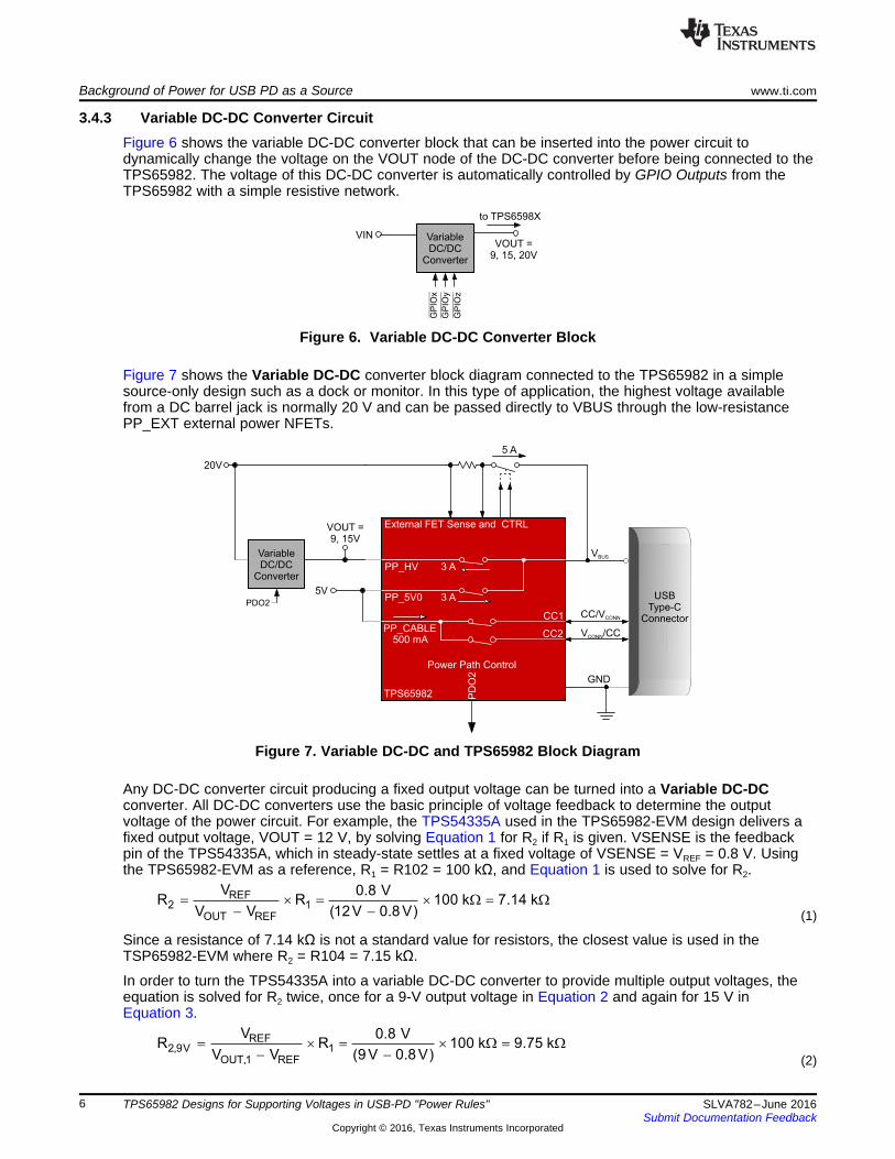
Figure 7 shows the Variable DC-DC converter block diagram connected to the TPS65982 in a simplesource-only design such as a dock or monitor. In this type of application, the highest voltage availablefrom a DC barrel jack is normally 20 V and can be passed directly to VBUS through the low-resistancePP_EXT external power NFETs.
Figure 7. Variable DC-DC and TPS65982 Block Diagram
Any DC-DC converter circuit producing a fixed output voltage can be turned into a Variable DC-DCconverter. All DC-DC converters use the basic principle of voltage feedback to determine the outputvoltage of the power circuit. For example, the TPS54335A used in the TPS65982-EVM design delivers afixed output voltage, VOUT = 12 V, by solving Equation 1 for R2 if R1 is given. VSENSE is the feedbackpin of the TPS54335A, which in steady-state settles at a fixed voltage of VSENSE = VREF = 0.8 V. Usingthe TPS65982-EVM as a reference, R1 = R102 = 100 kΩ, and Equation 1 is used to solve for R2.
(1)
Since a resistance of 7.14 kΩ is not a standard value for resistors, the closest value is used in theTSP65982-EVM where R2 = R104 = 7.15 kΩ.
In order to turn the TPS54335A into a variable DC-DC converter to provide multiple output voltages, theequation is solved for R2 twice, once for a 9-V output voltage in Equation 2 and again for 15 V inEquation 3.
(2)

0.1µFC48
0.1µF
C42
100kR102
0.1µFC45
DNPC52
DNPR101
DNPR103 GND
GND
GNDGND
GND 22µFC46
22µFC47
GND
47.5kR109
9.53kR108
91pFC50
1800pFC51
External Power
VSENSE
VSENSE
10uH
L4VIN
1
VSENSE6
EN8
RT10
GND3
COMP7
PH2
BOOT9
PAD11
GND4
GND5
U7
TPS54335ADRCR
22µFC44
383R45
A2
A1
B1
B2
Q8
100k
R55
13.32kR90
Default: 9V
GND
9.53kR104
PLUG_EVENT1000pFC53
GPIO0
GPIO6
A2
A1
B1
B2
Q11
21 Red
D7LED will indicate that the DCDC is activeand provide a minimum 50mA load forDCDC and discharging PPHV/EXT whenchanging PD contracts
~40ms to discharge from 20V to 5V
0.1µFC49
HV_Source
PD Contract: 15V
Copyright © 2016, Texas Instruments Incorporated
2,9 V 2,15 V
2 A2,9 V 2,15 V
R R 9.75 k 5.73 kR 15.32 k
R R 9.75 k 5.73 k
´ W ´ W= = = W
- W - W
2,9 V 2 A
2,15 V2,9 V 2 A
R RR
R R
´
=
+
REF2,15V 1
OUT,2 REF
V 0.8 VR R 100 k 5.63 k
V V (15 V 0.8 V)= ´ = ´ W = W
- -
www.ti.com Background of Power for USB PD as a Source
7SLVA782–June 2016Submit Documentation Feedback
Copyright © 2016, Texas Instruments Incorporated
TPS65982 Designs for Supporting Voltages in USB-PD "Power Rules"
(3)
The easiest way to realize this circuit is to keep the existing feedback circuit with R1 and the new R2,9V asthe default option and add another resistor in parallel with R2,9V that can be switched into the circuit when aGPIO is driven high. This resistor will be called R2A, where R2,9V // R2A = R2,15V. Equation 4 shows that R2,15Vis equivalent resistance of R2,9V in parallel with R2A, but the equation needs to solve for R2A because R2,15Vis already known. Equation 5 solves for R2A.
(4)
(5)
Figure 8 shows the circuit for using the TPS54335A as a variable DC-DC converter to deliver 9 V or 15 Vdepending on the USB PD contract negotiated as a PD Source. The GPIOs are automatically driven bythe TPS65982 when the FW is configured properly in the TPS6598X-CONFIG Configuration tool. Bydefault, 9 V is generated by R102 and R104, where R1 = R102 and R2,9V = R104 in the default feedbackvoltage divider in Equation 2. When a 15-V PD contract is negotiated, GPIO0 is driven high by theTPS65982 (not shown in this schematic), putting R90 in parallel with R104. The on-resistance of Q8 isnegligible compared to 13.32 kΩ, so the output of 15 V is generated by R102 and R104 // R90 where R1 =R102 and R2,15V = R2,9V // R2A = R104 // R90 = in Equation 4 and Equation 5.
Figure 8. TPS54335A Variable DC-DC Circuit for 9-V and 15-V Output Voltages
3.5 Dual-Role Port (DRP) Delivering 4+ Voltage RailsThe Power Multiplexer and the Variable DC-DC Converter discussed in the previous section will bothwork in many USB Type-C and PD applications, but the Variable DC-DC has advantages in a system withonly 1 Type-C port because less DC-DC buck converters are used and the overall component count isreduced significantly.
The Variable DC-DC buck converter can theoretically support as many different voltages as needed bythe application, so a DRP that needs to sink power on the PP_EXT FET path of the TPS65982 should beable to deliver 9 V, 15 V, and 20 V through the PP_HV FET path as a Source. Some applications will alsoneed to provide 12 Volts to support legacy USB PD devices that only accept a 12-V PD Contract.
The problem with a USB PD DRP that needs to provide 9 V, 12 V, 15 V, and 20 V from a single DC-DCconverter is that the DC barrel jack voltage is exactly 20 V and most DC-DC buck converters cannotsupport 100% Duty Cycle operation.
The next section explains in detail how that problem is solved and presents a design that will source thenew voltages to comply with the “Power Rules” of the latest USB PD Specification.

External FET Sense and CTRL
HostS
EL
EN
AM Mux Ctrl
TPS65982
PO
L
D±
D±SBU1/2
CC/VCONN
VBUS
GND
CC1/2
USB_TP/TN
USB_BP/BNSBU1/2
3 A 3 A
To SS Mux
VIN_3V3
5 A
PP_5V0
2Type-C Cable Detection and
USB PD Controller
222
USB 2.0 andSideband-Use
Data
HighSpeedMux
HostInterface
TPS54335A
TPS54335A
VOUT = 5, 9, 12, 15, 20 V
IOUT = 100 mAí5 A
VIN = 19.5í21 V
VOUT = 5 V
IOUT = 600 mAí3.5 A
VIN = 9í21 V
Fixed DC-DC
Fixed DC-DC
VOUT = 3.3 V
IOUT = 500 mA
VIN = 9í21 V
PD
O1
PD
O2
Voltage SelectP
DO
3
To Var DC-DC
PD
O0
GP
IOx
GP
IOy
LED Control
GP
IOz
To LED Drivers
LM3489Variable DC-DC
PD
O1
PD
O2
PD
O3
PD
O0
PP_HV
PP_CABLE
GND
J5
J6
(I2C, SPI)
VEXT = 20 V Typ. (19.5í22 V)
IEXT = 5 A (100 W Typ.)
DC Barrel Jack Input
USBType-C
Connector
VB
US
CC
1/C
C2
D+
/D-
SB
U1
/2S
S T
X/R
X
GND
J1
20-0000016-01Lintes Type-C Receptacle
TPS65982+LM3489 Variable DC-DC Converter for "Power Rules" Voltages www.ti.com
8 SLVA782–June 2016Submit Documentation Feedback
Copyright © 2016, Texas Instruments Incorporated
TPS65982 Designs for Supporting Voltages in USB-PD "Power Rules"
4 TPS65982+LM3489 Variable DC-DC Converter for "Power Rules" VoltagesThe block diagram in Figure 9 shows the TPS65982 controlling the LM3489 as a Variable DC-DC buckconverter to deliver 9, 12, 15, and 20 Volts through either the PP_HV internal high voltage path or thePP_EXT external high voltage path, while the path not used as a PD Source is used to sink power fromVBUS. As a result, this design can be used as a DRP that is capable of being line-powered from a barreljack or bus-powered over Type-C.
Figure 9. Block Diagram of TPS65982+LM3489 Variable DC-DC Design
The schematics for this design are shown in Figure 10 and Figure 11, where Figure 10 shows the powerpath containing the LM3489 and Figure 11 shows the Type-C connector and TPS65982 PD controller.GPIOs 0–3 are outputs from the TPS65982 that switch in the correct resistor in the LM3489 circuit todeliver the appropriate voltage when a Source PDO contract is negotiated. The LM3489 can achieve100% duty cycle because it is a Hysteretic PFET type of DC-DC buck controller, meaning that when 20 Vis required, the PFET is driven on 100% of the time and is effectively a switch that is closed.
GPIO6 is also an output from the TPS65982 that is used to drive the EN pin of the LM3489 high onlywhen a Type-C connection is present. GPIO6 simultaneously turns on LED D7, which is used to “bleed”the voltage from a higher voltage to a lower voltage when necessary. For example, the system may bedelivering 20 V to a laptop which is removed and quickly replaced with a tablet that only needs 9 V tocharge its battery. The TPS65982 automatically discharges VBUS to meet the USB PD specification, but ifLED D7 were not present, the PP_HV (or PP_EXT) node would be stuck at 20 V until it dischargesnaturally. This natural discharge could take seconds to minutes when an un-plug and re-plug event at theType-C port could happen in as little as 1 second.
Certain DC-DC converter ICs can perform this “voltage bleed” automatically, and this feature is referred toas “output discharge” or forced continuous conduction mode (FCCM). For more details on FCCM as a wayto remove LED D7 and save power, refer to the TPS53353 data sheet. The original high voltageNexFETsTM used in the TPS65982-EVM have been replaced with CSD87501L (Q1 in Figure 11), a singleback-to-back N-channel NexFET™ IC in a small WCSP package. The additional passive circuitry andconnectors in Figure 10 and Figure 11 not discussed in this application report are the same as theTPS65982-EVM.

0.1µFC26
0.1µF
C20
100kR82
0.1µFC23
DNPC27
DNPC30
DNPR81
DNPR83 GND
GND
GNDGND
GND
GND
0.1µFC37
0.1µF
C31
100kR92
19.1kR94
0.1µFC34
DNPC38
DNPC41
DNPR93 GND
GND
GNDGND
GND
GND
GND
GND
22µFC35
22µFC36
22µFC24
22µFC25
32.4kR84
SENSE1
GND4
POWER2
POWER3
GND5
SHIELD6
SHIELD7
SHIELD8
SHIELD9
J4
JPD1135-509-7F
VBarrel
GND
S3
1.00k
R27System_RESET
DNPR91
J9
47.5kR97
8.45kR95
100pFC39
2200pFC40
330pFC28
5600pFC29
2.74kR85
47.5kR88
System_3V3
System_5V
VBarrel
VBarrel
System_3V3
5V_VSENSE
5V_VSENSE
3V3_VSENSE
3V3_VSENSE
GND10uH
L3
10uH
L2
VIN1
VSENSE6
EN8
RT10
GND3
COMP7
PH2
BOOT9
PAD11
GND4
GND5
U6
TPS54335ADRCR
VIN1
VSENSE6
EN8
RT10
GND3
COMP7
PH2
BOOT9
PAD11
GND4
GND5
U5
TPS54335ADRCR GND
D10
22µFC22
22µFC33
30kR43
100k
R49 383R45
21 Red
D7
22µFC42
22µFC43
1000pFC45
GND
8.2kR42
0.1µFC44
GND
GND
A2
A1
B1
B2
Q8
A2
A1
B1
B2
Q9
A2
A1
B1
B2
Q10
100k
R55
100k
R87
100k
R89
2.20kR98
3.74kR96
9.31kR90
Plug Event resistance is always on for 5V and 5V PD ContractPlug Event Resistance & PDIOx resistance will be the equivalent resistance needed for Vfb
5V: 9.53k9V: 4.7k15V: 2.67k20V: 1.78k (Force 100% Duty Cycle)
Bottom Resistance Needed
Plug Event and ONLY ONE PDIOx are on for other PD contracts
PD Contract: 9V PD Contract: 15V PD Contract: 20VPD Contract: 5V
DCDC is disabled whenthere is no connection present
100µFC32
GND
LED will indicate that the DCDC is activeand provide a minimum 50mA load forDCDC and discharging PPHV/EXT whenchanging PD contracts
Output capacitors must be rated toat least 25V and have ESR in 100s of mOhms
When in 100% Duty Cycle (20V) the dropof the PFET and Inductor must be takeninto account. PP_EXT is recommended.
*The FB is set slightly higher for Vdrop*
~40ms to discharge from 20V to 5V
GND
GND
9.53kR52
PLUG_EVENT
VIN8
ADJ5
PGND6
GND2
ISEN1
PGATE7
EN3
FB4
U7
LM3489QMM/NOPB
270
R44
10µH
L4
D6PMEG3050EP,115
1000pFC46
VBarrel
GPIO0 GPIO2 GPIO3
PP_HV
PP_EXT
A2
A1
B1
B2
Q12
100k
R106
PD Contract: 12VGPIO1
5.36kR107
TP8 TP9 TP10TP11
GND
Labeled as GND
TP12
TP7
TP6
GPIO6
GPIO7DNPR170R16
Use R16 or R17 exclusive of each other
Place one of these next to the I2C
GPIO6
PLUG_EVENT
VAR_DCDC
A2
A1
B1
B2
Q11
100uFC47
GND
1
2
3
J9
61300311121
TP5
4
1
2
3Q7
SI8409DB-T1-E1
Copyright © 2016, Texas Instruments Incorporated
www.ti.com TPS65982+LM3489 Variable DC-DC Converter for "Power Rules" Voltages
9SLVA782–June 2016Submit Documentation Feedback
Copyright © 2016, Texas Instruments Incorporated
TPS65982 Designs for Supporting Voltages in USB-PD "Power Rules"
Figure 10. Power Path Schematic of TPS65982+LM3489 Variable DC-DC Design (Page 1 of 2)

GND GND
GNDGND
GND
D1
21 ohm
L1
0.01R1
GND
GND
GND
0R3
0R5
GND
1µFC6
10µFC1
VBUS
DNPR10
0R22
DNPR11
0R30
GND
0.01µFC7
0.01µFC8
0.01µFC9
0.01µFC10
D1+1
D1-2
NC6
NC7
NC9
NC10
D2+4
D2-5
GND3
GND8
U3
TPD4E05U06DQA
D1+1
D1-2
NC6
NC7
NC9
NC10
D2+4
D2-5
GND3
GND8
U4
TPD4E05U06DQA
0.22µFC3
3.83kR753.83kR76
3.83kR79
100kR26
0.01µFC53
GND
1.00kR121.00kR131.00kR141.00kR15
15.0kR28
White
12
D3
560R73
White
12
D4
560R74
White
12
D5
560R86
White
12
D2
560R72
GND
0R56
System_RESET
10µFC14
1µFC16
1µFC17
GND
1µFC13
System_3V3
LDO_3V3
GNDGND
GND
0.1µFC12
22µFC11
System_5V
GND
0.1µFC5
10µFC4
GND
PP_HV
1µFC18
PD & Alternate ModeConfiguration Switch
CC1/CC2 & SBU1/SBU2ESD Protection
USB2.0 Top/BottomESD Protection
30V Rated NFET Recommended
I2C Pull-Ups for I2C1 & I2C2
GND
GND
GNDGND
GND
GNDGND
9.09kR77
9.09kR78
3.83kR80
VOUT_3V3
LDO_1V8D
VBUS
VBUS
VBUS
VBUS
C_SBU_N
C_USB_B_N
C_USB_B_P
C_CC2C_SBU_P
C_USB_T_N
C_USB_T_P
C_CC1
LDO_3V3
I2C_SDA1
I2C_SDA2
I2C_SCL1
I2C_SCL2
I2C_IRQ1Z
I2C_IRQ2Z
C_SBU_N
C_USB_B_N
C_USB_B_P
C_CC2
C_SBU_P
C_USB_T_N
C_USB_T_P
C_CC1
C_USB_B_P
C_USB_B_N
C_USB_T_P
C_USB_T_N
C_CC2
C_CC1
C_SBU_N
C_SBU_P
GPIO0
C_CC2
C_CC1
C_USB_T_N
C_USB_T_P
C_USB_B_P
C_USB_B_N
C_SBU_N
C_SBU_P
MRESET
RESETZ
HV_GATE1
HV_GATE2
SENSEP
SENSEN
RPD_G2
RPD_G1
RPD_G1
RPD_G2
BUSPOWERZ
SENSEN
SENSEP
HV_GATE1 HV_GATE2
GPIO0
GPIO1
GPIO2
GPIO3
GPIO6
GPIO7
GPIO8
GPIO4_HPD
GPIO5_HPD
AUX_P
AUX_N
USB2_RP_P
USB2_RP_N
SPI_MOSI
SPI_MISO
SPI_CSZ
SPI_CLK
I2C_SDA1
I2C_SDA2
I2C_SCL1
I2C_SCL2
I2C_IRQ1Z
I2C_IRQ2ZGND
System_5V
CS1
DO/IO12
WP/IO23
GND4
DI/IO05
CLK6
HOLD/IO37
VCC8
U1
W25Q80DVSNIG
LDO_3V3
3.3kR4
3.3kR7
3.3kR9
SPI_MOSI
SPI_CLK
GND
SPI_MISO
LDO_3V3
SPI_CSZGND
0.1µF
C2
3.3kR8
SPI_SSZB3
SPI_MOSIB4
DEBUG_CTL2D5
UART_TXE2
DEBUG_CTL1E4
UART_RXF2
SWD_DATAF4
R_OSCG2
SWD_CLKG4
AUX_PJ1
AUX_NJ2
DEBUG2K2
DEBUG4K3
LSX_R2PL4
USB_RP_NK5
C_USB_TPK6
C_USB_BPK7
C_SBU1K8
RPD_G1K9
RPD_G2K10
DEBUG1L2
DEBUG3L3
LSX_P2RK4
USB_RP_PL5
C_USB_TNL6
C_USB_BNL7
C_SBU2L8
C_CC1L9
C_CC2L10
SPI_CLKA3
SPI_MISOA4
HV_GATE1B9
SENSEPB10
SSH7
HV_GATE2A9
SENSENA10
GPIO0B2
I2C_SCL2B5
I2C_IRQ2ZB6
I2C_IRQ1ZC1
GPIO1C2
GPIO4_HPDC10
I2C_SDA1D1
I2C_SCL1D2
GPIO7D7
GPIO2D10
GPIO5_HPDE10
MRESETE11
I2C_ADDRF1
RESETF11
GPIO6G10
GPIO3G11
GPIO8H6
NCL11
I2C_SDA2A5
RESETD6
U2A
TPS65982ABZQZR
GNDA1
PP_HVB7
GNDB8
PP_5V0B11
VDDIOB1
LDO_1V8DA2
PP_5V0C11
GNDD8
PP_5V0D11
LDO_BMCE1
GNDE5
GNDE6
GNDE7
GNDE8
GNDF5
GNDF6
GNDF7
GNDF8
BUSPOWERZF10
LDO_3V3G1
GNDG5
GNDG6
GNDG7
GNDG8
VIN_3V3H1
VOUT_3V3H2
GNDH4
GNDH5
GNDH8
PP_CABLEH10
VBUSH11
VBUSJ10
VBUSJ11
LDO_1V8AK1
VBUSK11
GNDL1
PP_HVA6
PP_HVA7
PP_HVA8
PP_5V0A11
U2B
TPS65982ABZQZR
150µFC21
GND
System_5V
330pFC19
330pFC15
GNDA1
TX1+A2
TX1-A3
VBUSA4
CC1A5
D+A6
D-A7
SBU1A8
VBUSA9
RX2-A10
RX2+A11
GNDA12
GNDB1
TX2+B2
TX2-B3
VBUSB4
CC2B5
D+B6
D-B7
SBU2B8
VBUSB9
RX1-B10
RX1+B11
GNDB12
H1H1
H2H2
H3H3
H4H4
H5H5
H6H6
11
22
33
J1
20-0000016-01
1
2
J6
ED120/2DSGND
Vbus_Sink
GPIO2 GPIO3GPIO1
1
2
3
4
5
6 7
8
9
10
11
12
S11.00kR991.00kR100
LDO_1V8D
LDO_3V3
BUSPOWERZ
GPIO0
GPIO1
GPIO2
GPIO3
A2
A1
B1
B2
Q3
A2
A1
B1
B2
Q4
A2
A1
B1
B2
Q5
A2
A1
B1
B2
Q6
Voltage LED Indicators
1 2
3 4
5 6
7 8
9 10
J10
5103308-1
I2C_SDA1
I2C_SCL1
SPI_MISO
SPI_CLK
SPI_CSZ
0R1100R111
DNPR108DNPR109
GND
I2C_SCL2
I2C_SDA2
0 R400 R690 R71
I2C_IRQ1Z
I2C_SDA1
I2C_SCL1
SPI_MOSI
Vbus_Sink
PP_HV
PP_EXT
1
2
3
J11
61300311121
1
2
3
J8
61300311121
1
J2
61300111121GND
TP4
TP3
TP1
TP2
A2A1
B2B1
C2
C1
D2D1
E2E1
Q1 CSD87501L
1.0MR211.0MR251.0MR291.0MR331.0MR101
100kR2
100kR6
100kR19
3.83kR18
LDO_3V3
GND
Copyright © 2016, Texas Instruments Incorporated
TPS65982+LM3489 Variable DC-DC Converter for "Power Rules" Voltages www.ti.com
10 SLVA782–June 2016Submit Documentation Feedback
Copyright © 2016, Texas Instruments Incorporated
TPS65982 Designs for Supporting Voltages in USB-PD "Power Rules"
Figure 11. Type-C and Power Delivery Schematic of TPS65982+LM3489 Variable DC-DC Design (Page 2 of 2)

www.ti.com Summary
11SLVA782–June 2016Submit Documentation Feedback
Copyright © 2016, Texas Instruments Incorporated
TPS65982 Designs for Supporting Voltages in USB-PD "Power Rules"
5 SummaryThis application report introduced the new voltages required by the “Power Rules” in the USB PD 2.0,Version 1.2 and PD 3.0 specifications, briefly discussed the numerous circuits that can be used to providethese voltages to VBUS as a PD Source, and selected the best option to use in a single Type-C portapplication with low cost as the primary goal.
Since the new design appears complex at first, a review of the voltage feedback principles of DC-DCcontroller ICs was needed to see that this solution is relatively simple to implement. Combining the GPIOOutput capabilities of the TSP65982 firmware and the ability of the LM3489 to deliver voltage at 100%duty cycle, a cost-competitive solution was designed and described in detail that will work in many Type-Cand PD Source, and DRP applications including notebooks, monitors, and docks.
6 References• TPS65982 data sheet (SLVSD02)• TPS65982 Evaluation Module user’s guide (SLVUAF8)• TPS6598X-CONFIG Configuration Tool• USB Power Delivery Specification• TPS54335A data sheet (SLVSCD5)• LM3489 data sheet (SNVS443)

IMPORTANT NOTICE
Texas Instruments Incorporated and its subsidiaries (TI) reserve the right to make corrections, enhancements, improvements and otherchanges to its semiconductor products and services per JESD46, latest issue, and to discontinue any product or service per JESD48, latestissue. Buyers should obtain the latest relevant information before placing orders and should verify that such information is current andcomplete. All semiconductor products (also referred to herein as “components”) are sold subject to TI’s terms and conditions of salesupplied at the time of order acknowledgment.TI warrants performance of its components to the specifications applicable at the time of sale, in accordance with the warranty in TI’s termsand conditions of sale of semiconductor products. Testing and other quality control techniques are used to the extent TI deems necessaryto support this warranty. Except where mandated by applicable law, testing of all parameters of each component is not necessarilyperformed.TI assumes no liability for applications assistance or the design of Buyers’ products. Buyers are responsible for their products andapplications using TI components. To minimize the risks associated with Buyers’ products and applications, Buyers should provideadequate design and operating safeguards.TI does not warrant or represent that any license, either express or implied, is granted under any patent right, copyright, mask work right, orother intellectual property right relating to any combination, machine, or process in which TI components or services are used. Informationpublished by TI regarding third-party products or services does not constitute a license to use such products or services or a warranty orendorsement thereof. Use of such information may require a license from a third party under the patents or other intellectual property of thethird party, or a license from TI under the patents or other intellectual property of TI.Reproduction of significant portions of TI information in TI data books or data sheets is permissible only if reproduction is without alterationand is accompanied by all associated warranties, conditions, limitations, and notices. TI is not responsible or liable for such altereddocumentation. Information of third parties may be subject to additional restrictions.Resale of TI components or services with statements different from or beyond the parameters stated by TI for that component or servicevoids all express and any implied warranties for the associated TI component or service and is an unfair and deceptive business practice.TI is not responsible or liable for any such statements.Buyer acknowledges and agrees that it is solely responsible for compliance with all legal, regulatory and safety-related requirementsconcerning its products, and any use of TI components in its applications, notwithstanding any applications-related information or supportthat may be provided by TI. Buyer represents and agrees that it has all the necessary expertise to create and implement safeguards whichanticipate dangerous consequences of failures, monitor failures and their consequences, lessen the likelihood of failures that might causeharm and take appropriate remedial actions. Buyer will fully indemnify TI and its representatives against any damages arising out of the useof any TI components in safety-critical applications.In some cases, TI components may be promoted specifically to facilitate safety-related applications. With such components, TI’s goal is tohelp enable customers to design and create their own end-product solutions that meet applicable functional safety standards andrequirements. Nonetheless, such components are subject to these terms.No TI components are authorized for use in FDA Class III (or similar life-critical medical equipment) unless authorized officers of the partieshave executed a special agreement specifically governing such use.Only those TI components which TI has specifically designated as military grade or “enhanced plastic” are designed and intended for use inmilitary/aerospace applications or environments. Buyer acknowledges and agrees that any military or aerospace use of TI componentswhich have not been so designated is solely at the Buyer's risk, and that Buyer is solely responsible for compliance with all legal andregulatory requirements in connection with such use.TI has specifically designated certain components as meeting ISO/TS16949 requirements, mainly for automotive use. In any case of use ofnon-designated products, TI will not be responsible for any failure to meet ISO/TS16949.
Products ApplicationsAudio www.ti.com/audio Automotive and Transportation www.ti.com/automotiveAmplifiers amplifier.ti.com Communications and Telecom www.ti.com/communicationsData Converters dataconverter.ti.com Computers and Peripherals www.ti.com/computersDLP® Products www.dlp.com Consumer Electronics www.ti.com/consumer-appsDSP dsp.ti.com Energy and Lighting www.ti.com/energyClocks and Timers www.ti.com/clocks Industrial www.ti.com/industrialInterface interface.ti.com Medical www.ti.com/medicalLogic logic.ti.com Security www.ti.com/securityPower Mgmt power.ti.com Space, Avionics and Defense www.ti.com/space-avionics-defenseMicrocontrollers microcontroller.ti.com Video and Imaging www.ti.com/videoRFID www.ti-rfid.comOMAP Applications Processors www.ti.com/omap TI E2E Community e2e.ti.comWireless Connectivity www.ti.com/wirelessconnectivity
Mailing Address: Texas Instruments, Post Office Box 655303, Dallas, Texas 75265Copyright © 2016, Texas Instruments Incorporated
Related Documents