® TOP221-227 TOPSwitch-II Family Three-terminal Off-line PWM Switch Figure 1. Typical Flyback Application. easier. The standard 8L PDIP packa ge option reduces cost in lower power, high effi ciency application s. The internal le ad frame of this package uses six of its pins to transfer heat from the chip directly to the board, eliminating the cost of a heat sink. TOPSwitch incorporates all functions necessary for a switched mode control system into a three terminal monolithic IC: power MOSFET, PWM controller, high voltage start up circuit, loop compensation and fault protection circuitry. Product Highlights • Lowest cost, lowest component count switcher solution • Cost competitive with linears above 5W • Very low AC/DC losses – up to 90% efficiency • Built-in Auto-restart and Current limiting • Latching Thermal shutdown for system level protection • Implements Flyback, Forward, Boost or Buck topology • Works with primary or opto feedback • Stable in discontinuous or continuous conduction mode • Source connected tab for low EMI • Circuit simplicity and Design Tools reduce time to market Description The second generation TOPSwitch-II family is more cost effective and provides several enhancements over the first generation TOPSwitch family. The TOPSwitch-II family extends the power range from 100W to 150W for 100/115/230 VAC input and from 50W to 90W for 85-265 VAC universal input. This brings TOPSwitch technology advantages to many new applications, i.e. TV, Monitor, Audio amplifiers, etc. Many significant circuit enhancements that reduce the sensitivity to board layout and line transients now make the design even PI-1951-091996 AC IN D S C CONTROL TOPSwitch ® 6 W 10 W 15 W 20 W TOP221Y TOP222Y TOP223Y TOP224Y TOP225Y TOP226Y TOP227Y 9 W 15 W 25 W 30 W TOP221P or TOP221G TOP222P or TOP222G TOP223P or TOP223G TOP224P or TOP224G OUTPUT POWER TABLE TO-220 (Y) Package 1 8L PDIP (P) or 8L SMD (G) Package 2 . P MAX 5,6 PART ORDER NUMBER Single Voltage Input 100/115/230 VAC ± 15% 3 Wide Range Input 85 to 265 VAC Single Voltage Input 100/115/230 VAC ± 15% 3 Wide Range Input 85 to 265 VAC P MAX 5,6 7 W 15 W 30 W 45 W 60 W 75 W 90 W P MAX 4,6 12 W 25 W 50 W 75 W 100 W 125 W 150 W P MAX 4,6 Notes: 1. Package outline: TO-220/3 2. Package Outline: DIP-8 or SMD-8 3. 100/115 VAC with doubler input 4. Assumes appropriate heat sinking to keep the maximum TOPSwitch junction temperature below 100 °C. 5. Soldered to 1 sq. in.( 6.45 cm 2 ), 2 oz. copper clad (610 gm/m 2 ) 6. P MAX is the maximum practical continuo us power output level for conditions shown. The continuous power capability in a given application depends on thermal environment, transformer design, efficiency require d, minimum specified input voltage, input storage capacitance, etc. 7. Refer to key application consideratio ns section when using TOPSwitch-II in an existing TOPSwitch design. PART ORDER NUMBER July 2001

Welcome message from author
This document is posted to help you gain knowledge. Please leave a comment to let me know what you think about it! Share it to your friends and learn new things together.
Transcript

8/2/2019 Top222g Pulse-width Modulation Switch
http://slidepdf.com/reader/full/top222g-pulse-width-modulation-switch 1/20
®
TOP221-227TOPSwitch-II FamilyThree-terminal Off-line PWM Switch
Figure 1. Typical Flyback Application.
easier. The standard 8L PDIP package option reduces cost in
lower power, high efficiency applications. The internal lead
frame of this package uses six of its pins to transfer heat from
the chip directly to the board, eliminating the cost of a heat sink.
TOPSwitch incorporates all functions necessary for a switched
mode control system into a three terminal monolithic IC: power
MOSFET, PWM controller, high voltage start up circuit, loop
compensation and fault protection circuitry.
Product Highlights
• Lowest cost, lowest component count switcher solution
• Cost competitive with linears above 5W
• Very low AC/DC losses – up to 90% efficiency
• Built-in Auto-restart and Current limiting
• Latching Thermal shutdown for system level protection
• Implements Flyback, Forward, Boost or Buck topology
• Works with primary or opto feedback
• Stable in discontinuous or continuous conduction mode
• Source connected tab for low EMI
• Circuit simplicity and Design Tools reduce time to market
Description
The second generation TOPSwitch-II family is more cost
effective and provides several enhancements over the first
generationTOPSwitchfamily. TheTOPSwitch-II family extends
the power range from 100W to 150W for 100/115/230 VAC
input and from 50W to 90W for 85-265 VAC universal input.
This brings TOPSwitch technology advantages to many new
applications, i.e. TV, Monitor, Audio amplifiers, etc. Many
significant circuit enhancements that reduce the sensitivity to
board layout and line transients now make the design even
PI-1951-091996
ACIN
D
S
CCONTROL
TOPSwitch
®
6 W
10 W
15 W
20 W
TOP221Y
TOP222Y
TOP223Y
TOP224Y
TOP225Y
TOP226Y
TOP227Y
9 W
15 W
25 W
30 W
TOP221P or TOP221G
TOP222P or TOP222G
TOP223P or TOP223G
TOP224P or TOP224G
OUTPUT POWER TABLE
TO-220 (Y) Package1 8L PDIP (P) or 8L SMD (G) Package2
.
PMAX
5,6
PART
ORDERNUMBER
Single Voltage Input100/115/230 VAC ±15%
3 Wide Range Input
85 to 265 VAC
Single Voltage Input100/115/230 VAC ±15%
3 Wide Range Input
85 to 265 VAC
PMAX
5,6
7 W
15 W
30 W
45 W
60 W
75 W
90 W
PMAX
4,6
12 W
25 W
50 W
75 W
100 W
125 W
150 W
PMAX
4,6
Notes: 1. Package outline: TO-220/3 2. Package Outline: DIP-8 or SMD-8 3. 100/115 VAC with doubler input 4. Assumes appropriateheat sinking to keep the maximum TOPSwitch junction temperature below 100 °C. 5. Soldered to 1 sq. in.( 6.45 cm2), 2 oz. copper clad(610 gm/m2) 6. P
MAXis the maximum practical continuous power output level for conditions shown. The continuous power capability
in a given application depends on thermal environment, transformer design, efficiency required, minimum specified input voltage, inputstorage capacitance, etc. 7. Refer to key application considerations section when using TOPSwitch-II in an existing TOPSwitch design.
PARTORDER
NUMBER
July 2001
8/2/2019 Top222g Pulse-width Modulation Switch
http://slidepdf.com/reader/full/top222g-pulse-width-modulation-switch 2/20
TOP221-227
D
7/012
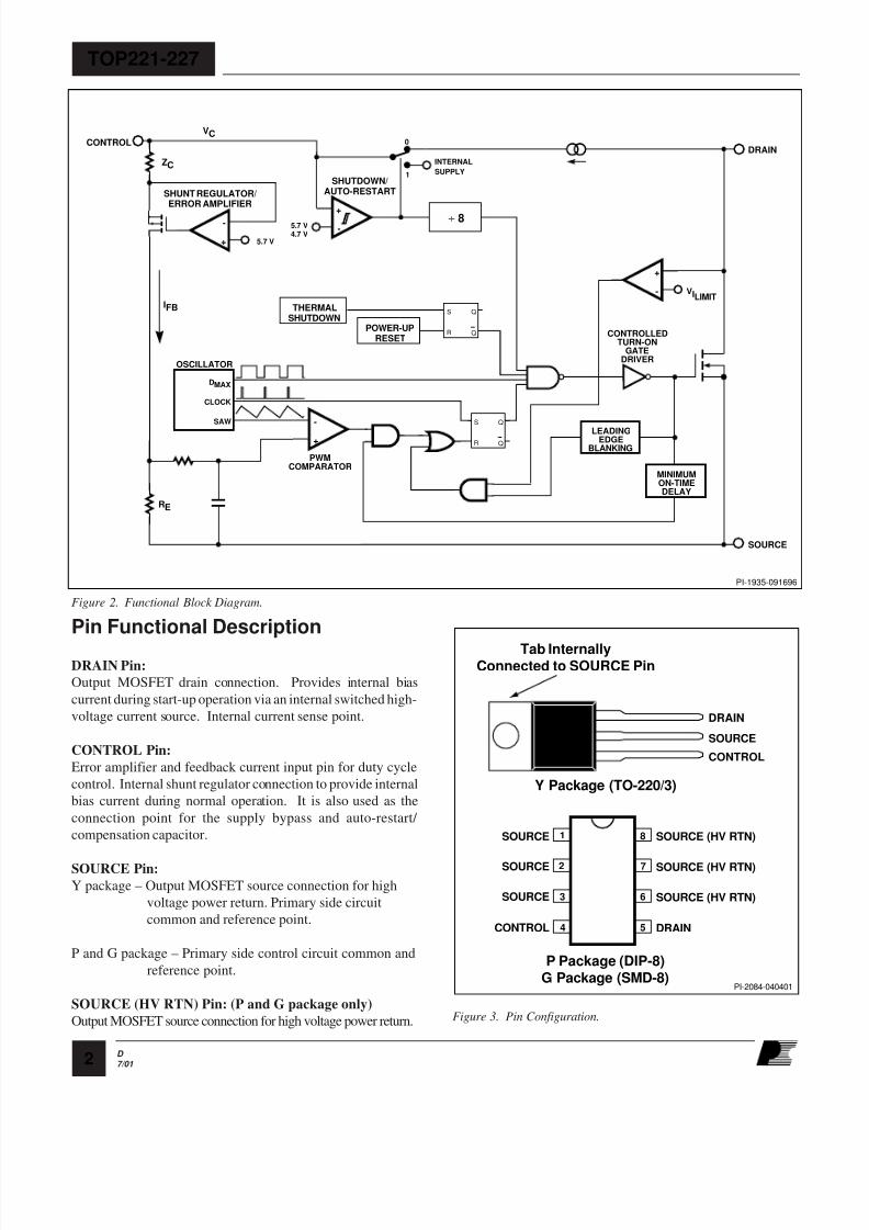
Figure 2. Functional Block Diagram.
Pin Functional Description
DRAIN Pin:
Output MOSFET drain connection. Provides internal bias
current during start-up operation via an internal switched high-
voltage current source. Internal current sense point.
CONTROL Pin:
Error amplifier and feedback current input pin for duty cycle
control. Internal shunt regulator connection to provide internal
bias current during normal operation. It is also used as the
connection point for the supply bypass and auto-restart/
compensation capacitor.
SOURCE Pin:
Y package – Output MOSFET source connection for high
voltage power return. Primary side circuit
common and reference point.
P and G package – Primary side control circuit common and
reference point.
SOURCE (HV RTN) Pin: (P and G package only)
Output MOSFET source connection for high voltage power return.
PI-1935-091696
SHUTDOWN/AUTO-RESTART
PWMCOMPARATOR
CLOCK
SAW
OSCILLATOR
CONTROLLEDTURN-ON
GATEDRIVER
INTERNAL
SUPPLY
5.7 V4.7 V
SOURCE
S
R
Q
Q
DMAX
-
+
CONTROL
-
+ 5.7 V
IFB
RE
ZC
VC
MINIMUMON-TIMEDELAY
+
- VILIMIT
LEADINGEDGE
BLANKING
POWER-UPRESET
S
R
Q
Q
÷ 8
0
1
THERMALSHUTDOWN
SHUNT REGULATOR/ERROR AMPLIFIER
+
-
DRAIN
PI-2084-040401
CONTROL
DRAIN
SOURCE
Y Package (TO-220/3)
Tab InternallyConnected to SOURCE Pin
CONTROL
8
5
7
6
DRAIN
SOURCE (HV RTN)
SOURCE
SOURCE
1
4
2
3
SOURCE (HV RTN)
SOURCE (HV RTN)SOURCE
P Package (DIP-8)G Package (SMD-8)
Figure 3. Pin Configuration.
8/2/2019 Top222g Pulse-width Modulation Switch
http://slidepdf.com/reader/full/top222g-pulse-width-modulation-switch 3/20
TOP221-227
D
7/01 3
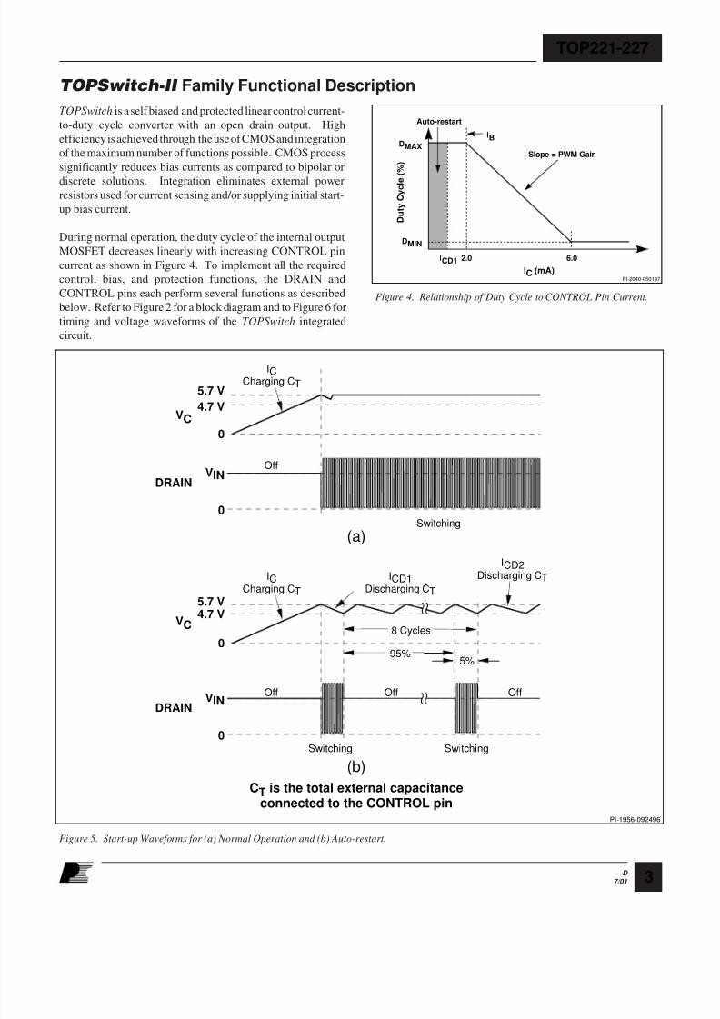
TOPSwitch-II Family Functional Description
TOPSwitch is a self biased and protected linear control current-
to-duty cycle converter with an open drain output. High
efficiency is achieved through the use of CMOS and integration
of the maximum number of functions possible. CMOS process
significantly reduces bias currents as compared to bipolar or
discrete solutions. Integration eliminates external powerresistors used for current sensing and/or supplying initial start-
up bias current.
During normal operation, the duty cycle of the internal output
MOSFET decreases linearly with increasing CONTROL pin
current as shown in Figure 4. To implement all the required
control, bias, and protection functions, the DRAIN and
CONTROL pins each perform several functions as described
below. Refer to Figure 2 for a block diagram and to Figure 6 for
timing and voltage waveforms of the TOPSwitch integrated
circuit.
PI-2040-050197
DMAX
DMIN
D u t y C y c l e
( % )
IC (mA)
2.0 6.0
Slope = PWM Gain
IB
ICD1
Auto-restart
Figure 4. Relationship of Duty Cycle to CONTROL Pin Current.
DRAIN
0
VIN
VC
0
4.7 V5.7 V
8 Cycles
95%5%
Off
Switching Switching
Off
ICCharging CT
ICD1Discharging CT
ICD2Discharging CT
ICCharging CT
Off
PI-1956-092496
DRAIN
0
VIN
VC
0
4.7 V
5.7 V
Off
Switching
(b)
(a)
CT is the total external capacitanceconnected to the CONTROL pin
Figure 5. Start-up Waveforms for (a) Normal Operation and (b) Auto-restart.

8/2/2019 Top222g Pulse-width Modulation Switch
http://slidepdf.com/reader/full/top222g-pulse-width-modulation-switch 4/20
TOP221-227
D
7/014
Control Voltage Supply
CONTROL pin voltage VC
is the supply or bias voltage for the
controller and driver circuitry. An external bypass capacitor
closely connected between the CONTROL and SOURCE pins
is required to supply the gate drive current. The total amount
of capacitance connected to this pin (CT) also sets the auto-restart timing as well as control loop compensation. V
Cis
regulated in either of two modes of operation. Hysteretic
regulation is used for initial start-up and overload operation.
Shunt regulation is used to separate the duty cycle error signal
from the control circuit supply current. During start-up,
CONTROL pin current is supplied from a high-voltage switched
current source connected internally between the DRAIN and
CONTROL pins. The current source provides sufficient current
to supply the control circuitry as well as charge the total
external capacitance (CT).
The first time VC
reaches the upper threshold, the high-voltage
current source is turned off and the PWM modulator and output
transistor are activated, as shown in Figure 5(a). During normal
operation (when the output voltage is regulated) feedback
control current supplies the VC
supply current. The shunt
regulator keeps VC
at typically 5.7 V by shunting CONTROL
pin feedback current exceeding the required DC supply current
through the PWM error signal sense resistor RE. The low
dynamic impedance of this pin (ZC) sets the gain of the error
amplifier when used in a primary feedback configuration. The
dynamic impedance of the CONTROL pin together with the
external resistance and capacitance determines the control loop
compensation of the power system.
If the CONTROL pin total external capacitance (CT) should
discharge to the lower threshold, the output MOSFET is turned
off and the control circuit is placed in a low-current standby
mode. The high-voltage current source turns on and charges the
external capacitance again. Charging current is shown with a
negative polarity and discharging current is shown with a
positive polarity in Figure 6. The hysteretic auto-restart
comparator keeps VC
within a window of typically 4.7 to 5.7 V
by turning the high-voltage current source on and off as shown
in Figure 5(b). The auto-restart circuit has a divide-by-8
counter which prevents the output MOSFET from turning on
again until eight discharge-charge cycles have elapsed. The
counter effectively limits TOPSwitch power dissipation byreducing the auto-restart duty cycle to typically 5%. Auto-
restart continues to cycle until output voltage regulation is
again achieved.
Bandgap Reference
All critical TOPSwitch internal voltages are derived from a
temperature-compensated bandgap reference. This reference
is also used to generate a temperature-compensated current
source which is trimmed to accurately set the oscillator frequency
and MOSFET gate drive current.
Oscillator
The internal oscillator linearly charges and discharges the
internal capacitance between two voltage levels to create a
sawtooth waveform for the pulse width modulator. The oscillator
sets the pulse width modulator/current limit latch at the beginning
of each cycle. The nominal frequency of 100 kHz was chosento minimize EMI and maximize efficiency in power supply
applications. Trimming of the current reference improves the
frequency accuracy.
Pulse Width Modulator
The pulse width modulator implements a voltage-mode control
loop by driving the output MOSFET with a duty cycle inversely
proportional to the current into the CONTROL pin which
generates a voltage error signal across RE. The error signal
across RE
is filtered by an RC network with a typical corner
frequency of 7 kHz to reduce the effect of switching noise. The
filtered error signal is compared with the internal oscillator
sawtooth waveform to generate the duty cycle waveform. As
the control current increases, the duty cycle decreases. A clock
signal from the oscillator sets a latch which turns on the output
MOSFET. The pulse width modulator resets the latch, turning
off the output MOSFET. The maximum duty cycle is set by the
symmetry of the internal oscillator. The modulator has a
minimum ON-time to keep the current consumption of the
TOPSwitchindependent of the error signal. Note that a minimum
current must be driven into the CONTROL pin before the duty
cycle begins to change.
Gate Driver
The gate driver is designed to turn the output MOSFET on at acontrolled rate to minimize common-mode EMI. The gate drive
current is trimmed for improved accuracy.
Error Amplifier
The shunt regulator can also perform the function of an error
amplifier in primary feedback applications. The shunt regulator
voltage is accurately derived from the temperature compensated
bandgap reference. The gain of the error amplifier is set by the
CONTROL pin dynamic impedance. The CONTROL pin
clamps external circuit signals to the VC
voltage level. The
CONTROL pin current in excess of the supply current is
separated by the shunt regulator and flows through RE
as a
voltage error signal.
Cycle-By-Cycle Current Limit
The cycle by cycle peak drain current limit circuit uses the
output MOSFET ON-resistance as a sense resistor. A current
limit comparator compares the output MOSFET ON-state drain-
source voltage, VDS(ON)
with a threshold voltage. High drain
current causes VDS(ON)
to exceed the threshold voltage and turns
the output MOSFET off until the start of the next clock cycle.
The current limit comparator threshold voltage is temperature
TOPSwitch-II Family Functional Description (cont.)
8/2/2019 Top222g Pulse-width Modulation Switch
http://slidepdf.com/reader/full/top222g-pulse-width-modulation-switch 5/20
TOP221-227
D
7/01 5
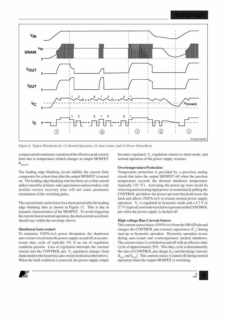
PI-2030-042397
VIN
VOUT0
IOUT0
1 2 131
DRAIN
0
VIN
VC0
• • • • • •1 2 1 2 8 1
0IC • • • • • •
1 2
8
8 1 2 8 1
VC(reset)
compensated to minimize variation of the effective peak current
limit due to temperature related changes in output MOSFET
RDS(ON)
.
The leading edge blanking circuit inhibits the current limit
comparator for a short time after the output MOSFET is turned
on. The leading edge blanking time has been set so that current
spikes caused by primary-side capacitances and secondary-side
rectifier reverse recovery time will not cause premature
termination of the switching pulse.
The current limit can be lower for a short period after the leading
edge blanking time as shown in Figure 12. This is due to
dynamic characteristics of the MOSFET. To avoid triggering
the current limit in normal operation, the drain current waveform
should stay within the envelope shown.
Shutdown/Auto-restart
To minimize TOPSwitch power dissipation, the shutdown/
auto-restart circuit turns the power supply on and off at an auto-
restart duty cycle of typically 5% if an out of regulation
condition persists. Loss of regulation interrupts the external
current into the CONTROL pin. VC
regulation changes from
shunt mode to the hysteretic auto-restart mode described above.
When the fault condition is removed, the power supply output
becomes regulated, VC
regulation returns to shunt mode, and
normal operation of the power supply resumes.
Overtemperature ProtectionTemperature protection is provided by a precision analog
circuit that turns the output MOSFET off when the junction
temperature exceeds the thermal shutdown temperature
(typically 135 °C). Activating the power-up reset circuit by
removing and restoring input power or momentarily pulling the
CONTROL pin below the power-up reset threshold resets the
latch and allows TOPSwitch to resume normal power supply
operation. VC
is regulated in hysteretic mode and a 4.7 V to
5.7 V (typical) sawtooth waveform is present on the CONTROL
pin when the power supply is latched off.
High-voltage Bias Current Source
This current source biases TOPSwitch from the DRAIN pin andcharges the CONTROL pin external capacitance (C
T) during
start-up or hysteretic operation. Hysteretic operation occurs
during auto-restart and overtemperature latched shutdown.
The current source is switched on and off with an effective duty
cycle of approximately 35%. This duty cycle is determined by
the ratio of CONTROL pin charge (IC) and discharge currents
(ICD1
and ICD2
). This current source is turned off during normal
operation when the output MOSFET is switching.
Figure 6. Typical Waveforms for (1) Normal Operation, (2) Auto-restart, and (3) Power Down Reset.

8/2/2019 Top222g Pulse-width Modulation Switch
http://slidepdf.com/reader/full/top222g-pulse-width-modulation-switch 6/20
TOP221-227
D
7/016
Figure 7. Schematic Diagram of a 4 W TOPSwitch-II Standby Power Supply using an 8 lead PDIP.
Application Examples
Following are just two of the many possible TOPSwitch
implementations. Refer to the Data Book and Design Guide
for additional examples.
4 W Standby Supply using 8 Lead PDIP
Figure 7 shows a 4 W standby supply. This supply is used in
appliances where certain standby functions (e.g. real time
clock, remote control port) must be kept active even while the
main power supply is turned off.
The 5 V secondary is used to supply the standby function and
the 12 V non-isolated output is used to supply power for the
PWM controller of the main power supply and other primary
side functions.
For this application the input rectifiers and input filter are sized
for the main supply and are not shown. The input DC rail may
vary from 100 V to 380 V DC which corresponds to the full
universal AC input range. The TOP221 is packaged in an 8 pin
power DIP package.
The output voltage (5 V) is directly sensed by the Zener diode
(VR1) and the optocoupler (U2). The output voltage is determinedby the sum of the Zener voltage and the voltage drop across the
LED of the optocoupler (the voltage drop across R1 is negligible).
The output transistor of the optocoupler drives the CONTROL
pin of the TOP221. C5 bypasses the CONTROL pin and provides
control loop compensation and sets the auto-restart frequency.
The transformer’s leakage inductance voltage spikes are snubbed
by R3 and C1 through diode D1. The bias winding is rectified
and filtered by D3 and C4 providing a non-isolated 12 V output
which is also used to bias the collector of the optocoupler’s
output transistor. The isolated 5 V output winding is rectified by
D2 and filtered by C2, L1 and C3.
Wide-RangeDC Input
D
S
CCONTROL
PI-2115-040401
+
-
R347 kΩ
D1UF4005
C12.2 nF1 kV
D2UF5401
TOP221P
L13.3 µH
D31N4148
C4100µF16 V
U2PC817A
R110Ω
C3100 µF10 V
+5 V
C547 µF10 V
C2330 µF10 V
U1
R2100 Ω
VR1
TOPSwitch-II
T1
RTN
+
-
12 V Non-Isolated

8/2/2019 Top222g Pulse-width Modulation Switch
http://slidepdf.com/reader/full/top222g-pulse-width-modulation-switch 7/20
TOP221-227
D
7/01 7
20 W Universal Supply using 8 Lead PDIP
Figure 8 shows a 12 V, 20 W secondary regulated flyback power
supply using the TOP224P in an eight lead PDIP package and
operating from universal 85 to 265 VAC input voltage. This
example demonstrates the advantage of the higher power 8 pin
leadframe used with the TOPSwitch-II family. This low cost
package transfers heat directly to the board through six source
pins, eliminating the heatsink and the associated cost. Efficiencyis typically 80% at low line input. Output voltage is directly
sensed by optocoupler U2 and Zener diode VR2. The output
voltage is determined by the Zener diode (VR2) voltage and the
voltage drops across the optocoupler (U2) LED and resistor R1.
Other output voltages are possible by adjusting the transformer
turns ratio and value of Zener diode VR2.
AC power is rectified and filtered by BR1 and C1 to create the
high voltage DC bus applied to the primary winding of T1. The
other side of the transformer primary is driven by the integrated
TOPSwitch-II high-voltage MOSFET. D1 and VR1 clamp
leading-edge voltage spikes caused by transformer leakage
inductance. The power secondary winding is rectified and
filtered by D2, C2, L1, and C3 to create the 12 V output voltage.
R2 and VR2 provide a slight pre-load on the 12 V output to
improve load regulation at light loads. The bias winding is
rectified and filtered by D3 and C4 to create a TOPSwitch bias
voltage. L2 and Y1-safety capacitor C7 attenuate commonmode emission currents caused by high voltage switching
waveforms on the DRAIN side of the primary winding and the
primary to secondary capacitance. Leakage inductance of L2
with C1 and C6 attenuates differential-mode emission currents
caused by the fundamental and harmonics of the trapezoidal or
triangular primary current waveform. C5 filters internal
MOSFET gate drive charge current spikes on the CONTROL
pin, determines the auto-restart frequency, and together with
R1 and R3, compensates the control loop.
Figure 8. Schematic Diagram of a 20 W Universal Input TOPSwitch-II Power Supply using an 8 lead PDIP.
PI-2019-033197
D2MUR420
D31N4148
C2330 µF35 V
C3220 µF35 V
T1
D1BYV26C
VR1P6KE200
VR21N5241B
11 V
R2220 Ω
BR1400 V
C147 µF400 V
F13.15 AJ1
C60.1 µF
250 VAC
L222 mH
L
N
C547 µF
U1TOP224PD
S
CCONTROL
TOPSwitch-II
R36.8 Ω
L13.3 µH
C40.1 µF
U2PC817A
R1100 Ω
C71 nF
250 VACY1
+12 V
RTN

8/2/2019 Top222g Pulse-width Modulation Switch
http://slidepdf.com/reader/full/top222g-pulse-width-modulation-switch 8/20
TOP221-227
D
7/018
Key Application Considerations
General Guidelines
• Keep the SOURCE pin length very short. Use a Kelvin
connection to the SOURCE pin for the CONTROL pin
bypass capacitor. Use single point grounding techniques atthe SOURCE pin as shown in Figure 9.
•Minimize peak voltage and ringing on the DRAIN voltage
at turn-off. Use a Zener or TVS Zener diode to clamp the
drain voltage below the breakdown voltage rating of
TOPSwitch under all conditions, including start-up and
overload. The maximum recommended clamp Zener
voltage for the TOP2XX series is 200 V and the
corresponding maximum reflected output voltage on the
primary is 135 V. Please see Step 4: AN-16 in the 1996-97
Data Book and Design Guide or on our Web site.
• The transformer should be designed such that the rate of change of drain current due to transformer saturation is
within the absolute maximum specification (∆ID
in 100 ns
before turn off as shown in Figure 13). As a guideline, for
most common transformer cores, this can be achieved by
maintaining the Peak Flux Density (at maximum ILIMIT
current) below 4200 Gauss (420 mT). The transformer
spreadsheets Rev. 2.1 (or later) for continuous and Rev.1.0
(or later) for discontinuous conduction mode provide the
necessary information.
• Do not plug TOPSwitch into a “hot” IC socket during test.
External CONTROL pin capacitance may be charged to
excessive voltage and cause TOPSwitch damage.
• While performing TOPSwitch device tests, do not exceed
maximum CONTROL pin voltage of 9 V or maximum
CONTROL pin current of 100 mA.
•Under some conditions, externally provided bias or supply
current driven into the CONTROL pin can hold the
TOPSwitch in one of the 8 auto-restart cycles indefinitely
and prevent starting. To avoid this problem when doing
bench evaluations, it is recommended that the VC
power
supply be turned on before the DRAIN voltage is applied.
TOPSwitch can also be reset by shorting the CONTROL
pin to the SOURCE pin momentarily.
• CONTROL pin currents during auto-restart operation are
much lower at low input voltages (< 36 V) which increases
the auto-restart cycle time (see the IC
vs. DRAIN Voltage
Characteristic curve).
• Short interruptions of AC power may cause TOPSwitch to
enter the 8-count auto-restart cycle before starting again.
This is because the input energy storage capacitors are not
completely discharged and the CONTROL pin capacitance
has not discharged below the internal power-up resetvoltage.
• In some cases, minimum loading may be necessary to keep
a lightly loaded or unloaded output voltage within the
desired range due to the minimum ON-time.
ReplacingTOPSwitch with TOPSwitch-II
There is no external latching shutdown function in
TOPSwitch-II. Otherwise, the functionality of the
TOPSwitch-II devices is same as that of the TOPSwitch family.
However, before considering TOPSwitch-II as a 'drop in'
replacement in an existing TOPSwitch design, the designshould be verified as described below.
The new TOPSwitch-II family offers more power capability
than the original TOPSwitch family for the same MOSFET
RDS(ON)
. Therefore, the original TOPSwitch design must be
reviewed to make sure that the selected TOPSwitch-II
replacement device and other primary components are not over
stressed under abnormal conditions.
The following verification steps are recommended:
• Check the transformer design to make sure that it meets the
∆ID specification as outlined in the General Guidelinessection above.
• Thermal: Higher power capability of the TOPSwitch-II
would in many instances allow use of a smaller MOSFET
device (higher RDS(ON)
) for reduced cost. This may affect
TOPSwitchpower dissipation and power supply efficiency.
Therefore thermal performance of the power supply must
be verified with the selected TOPSwitch-II device.
• Clamp Voltage: Reflected and Clamp voltages should be
verified not to exceed recommended maximums for the
TOP2XX Series: 135 V Reflected/200 V Clamp. Please
see Step 4: AN-16 in the Data Book and Design Guide and
readme.txt file attached to the transformer design
spreadsheets.
•Agency Approval: Migrating to TOPSwitch-II may require
agency re-approval.

8/2/2019 Top222g Pulse-width Modulation Switch
http://slidepdf.com/reader/full/top222g-pulse-width-modulation-switch 9/20
TOP221-227
D
7/01 9
Figure 9. Recommended TOPSwitch Layout.
PI-2021-041798
PC Board
Kelvin-connected
auto-restart/bypass capacitor C5
and/or compensation network
Bias/Feedback Input
Bias/Feedback Return
High-voltage Return
Bend DRAIN pin
forward if neededfor creepage.
D R A I N
S O U R C E
C ON T R OL
Do not bend SOURCE pin.
Keep it short.
High Voltage
Return
Bias/Feedback
Return
DSC
Bias/FeedbackInput
CONTROL
SOURCE
SOURCE
DRAIN
TOP VIEW
High Voltage
Return
Bias/FeedbackReturn
Bias/Feedback
Input
DIP-8/SMD-8 PACKAGE
TO-220 PACKAGE
TOP VIEW
C5
Kelvin-connectedauto-restart/bypass capacitor C5
and/or compensation network
Kelvin-connectedauto-restart/bypass
capacitor C5and/or compensation
network
C5
C5
Design Tools
The following tools available from Power Integrations greatly
simplify TOPSwitch based power supply design.
•Data Book and Design Guide includes extensive application
information
• Excel Spreadsheets for Transformer Design - Use of this
tool is strongly recommended for allTOPSwitchdesigns.
• Reference design boards – Production viable designs that
are assembled and tested.
All data sheets, application literature and up-to-date versions of
the Transformer Design Spreadsheets can be downloaded from
our Web site at www.powerint.com. A diskette of the
Transformer Design Spreadsheets may also be obtained by
sending in the completed form provided at the end of this data
sheet.

8/2/2019 Top222g Pulse-width Modulation Switch
http://slidepdf.com/reader/full/top222g-pulse-width-modulation-switch 10/20
TOP221-227
D
7/0110
ABSOLUTE MAXIMUM RATINGS(1)
DRAIN Voltage ............................................ -0.3 to 700 V
DRAIN Current Increase (∆ID) in 100 ns except during
blanking time ......................................... 0.1 x ILIMIT(MAX)
(2)
CONTROL Voltage ..................................... - 0.3 V to 9 V
CONTROL Current ...............................................100 mAStorage Temperature ..................................... -65 to 150 °C
Notes:
1. All voltages referenced to SOURCE, TA
= 25 °C.
2. Related to transformer saturation – see Figure 13.
3. Normally limited by internal circuitry.
4. 1/16" from case for 5 seconds.
Operating Junction Temperature(3) ................ -40 to 150 °C
Lead Temperature(4) ................................................ 260 °C
Thermal Impedance: Y Package (θJA
)(5) .................70 °C/W
(θJC
)(6) ...................2 °C/W
P/G Package:
(θJA
) .........45 °C/W(7); 35 °C/W(8)
(θJC
)(6)...............................11 °C/W
5. Free standing with no heatsink.
6. Measured at tab closest to plastic interface or SOURCE pin.
7. Soldered to 0.36 sq. inch (232 mm2), 2 oz. (610 gm/m2) copper clad.
8. Soldered to 1 sq. inch (645 mm2), 2 oz. (610 gm/m2) copper clad.
90 100 110
64 67 70
0.7 1.7 2.7
-21 -16 -11
-0.05
0.8 2.0 3.3
10 15 22
0.18
-2.4 -1.9 -1.2
-2 -1.5 -0.8
0.4
fOSC
DMAX
DMIN
IB
ZC
IC
CONTROL FUNCTIONS
OutputFrequency
MaximumDuty Cycle
MinimumDuty Cycle
PWMGain
PWM GainTemperature Drift
ExternalBias Current
DynamicImpedance
Dynamic ImpedanceTemperature Drift
CONTROL PinCharging Current
Charging CurrentTemperature Drift
kHz
%
%
%/mA
%/mA/ °C
mA
Ω
%/ °C
mA
%/ °C
SHUTDOWN/AUTO-RESTART
Conditions
(Unless Otherwise Specified)
See Figure 14
SOURCE = 0 V; TJ = -40 to 125 °C
Min Typ MaxParameter Symbol Units
IC
= 4 mA, TJ
= 25 °C
IC
= ICD1
+ 0.4 mA, See Figure 10
IC
= 10 mA, See Figure 10
IC = 4 mA, TJ = 25 °C
See Figure 4
See Note A
See Figure 4
IC
= 4 mA, TJ
= 25 °C
See Figure 11
VC
= 0 VT
J= 25 °C
VC
= 5 V
See Note A

8/2/2019 Top222g Pulse-width Modulation Switch
http://slidepdf.com/reader/full/top222g-pulse-width-modulation-switch 11/20
TOP221-227
D
7/01 11
5.7
4.4 4.7 5.0
0.6 1.0
2 5 9
2 5 8
1.2
0.23 0.25 0.28
0.45 0.50 0.55
0.90 1.00 1.10
1.35 1.50 1.65
1.80 2.00 2.20
2.25 2.50 2.75
2.70 3.00 3.30
0.75 x
ILIMIT(MIN)
180
VC(AR)
ILIMIT
IINIT
tLEB
SHUTDOWN/AUTO-RESTART (cont.)
Auto-restartThreshold Voltage
UV LockoutThreshold Voltage
Auto-restartHysteresis Voltage
Auto-restartDuty Cycle
Auto-restartFrequency
Self-protectionCurrent Limit
Initial CurrentLimit
Leading EdgeBlanking Time
CIRCUIT PROTECTION
V
V
V
%
Hz
A
A
ns
≤ 85 VAC
(Rectified Line Input)
265 VAC
(Rectified Line Input)
0.6 x
ILIMIT(MIN)
Conditions
(Unless Otherwise Specified)
See Figure 14
SOURCE = 0 V; TJ
= -40 to 125 °C
Min Typ MaxParameter Symbol Units
TOP221-222
TOP223-227
S1 open
S1 open
S1 open
S1 open
S1 open
di/dt = 40 mA/ µs, TOP221Y
TJ= 25 °C TOP221P or G
di/dt = 80 mA/ µs, TOP222Y
TJ
= 25 °C TOP222P or G
di/dt = 160 mA/ µs, TOP223Y
TJ
= 25 °C TOP223P or G
di/dt = 240 mA/ µs, TOP224Y
TJ
= 25 °C TOP224P or G
di/dt = 320 mA/ µs,TOP225Y
TJ= 25 °C
di/dt = 400 mA/ µs,TOP226Y
TJ= 25 °C
di/dt = 480 mA/ µs,TOP227Y
TJ = 25 °C
See Figure 12T
J= 25 °C
IC
= 4 mA,
TJ
= 25 °C
8/2/2019 Top222g Pulse-width Modulation Switch
http://slidepdf.com/reader/full/top222g-pulse-width-modulation-switch 12/20
TOP221-227
D
7/0112
tILD
VC(RESET)
RDS(ON)
IDSS
BVDSS
tR
tF
100
125 135
2.0 3.3 4.3
31.2 36.0
51.4 60.0
15.6 18.0
25.7 30.0
7.8 9.0
12.9 15.0
5.2 6.0
8.6 10.0
3.9 4.56.4 7.5
3.1 3.6
5.2 6.0
2.6 3.0
4.3 5.0
250
700
100
50
Current LimitDelay
Thermal ShutdownTemperature
Power-up ResetThreshold Voltage
ON-StateResistance
OFF-StateCurrent
BreakdownVoltage
RiseTime
FallTime
ns
°C
V
Ω
µA
V
ns
ns
CIRCUIT PROTECTION (cont.)
OUTPUT
Conditions
(Unless Otherwise Specified)
See Figure 14
SOURCE = 0 V; TJ
= -40 to 125 °C
Min Typ MaxParameter Symbol Units
IC
= 4 mA
IC
= 4 mA
S2 open
TOP221 TJ = 25 °C
ID
= 25 mA TJ
= 100 °C
TOP222 TJ
= 25 °C
ID
= 50 mA TJ
= 100 °C
TOP223 TJ
= 25 °C
ID
= 100 mA TJ
= 100 °C
TOP224 TJ
= 25 °C
ID
= 150 mA TJ
= 100 °C
TOP225 TJ
= 25 °C
ID
= 200 mA TJ
= 100 °C
TOP226 TJ
= 25 °C
ID
= 250 mA TJ
= 100 °C
TOP227 TJ
= 25 °C
ID
= 300 mA TJ
= 100 °C
See Note B
VDS
= 560 V, TA
= 125 °C
See Note B
ID
= 100 µA, TA
= 25 °C
Measured in a Typical Flyback
Converter Application.

8/2/2019 Top222g Pulse-width Modulation Switch
http://slidepdf.com/reader/full/top222g-pulse-width-modulation-switch 13/20
TOP221-227
D
7/01 13
VC(SHUNT)
ICD1
ICD2
36
5.5 5.7 6.0
±50
0.6 1.2 1.6
0.7 1.4 1.8
0.5 0.8 1.1
DRAIN SupplyVoltage
Shunt RegulatorVoltage
Shunt RegulatorTemperature Drift
CONTROL Supply/ Discharge Current
V
V
ppm/ °C
mA
OUTPUT (cont.)
NOTES:
A. For specifications with negative values, a negative temperature coefficient corresponds to an increase inmagnitude with increasing temperature, and a positive temperature coefficient corresponds to a decrease inmagnitude with increasing temperature.
B. The breakdown voltage and leakage current measurements can be accomplished as shown in Figure 15 by using
the following sequence:
i. The curve tracer should initially be set at 0 V. The base output should be adjusted through a voltage sequenceof 0 V, 6.5 V, 4.3 V, and 6.5 V, as shown. The base current from the curve tracer should not exceed 100 mA. This
CONTROL pin sequence interrupts the Auto-restart sequence and locks the TOPSwitch internal MOSFET in theOFF State.
ii. The breakdown and the leakage measurements can now be taken with the curve tracer. The maximum
voltage from the curve tracer must be limited to 700 V under all conditions.
C. It is possible to start up and operate TOPSwitch at DRAIN voltages well below 36 V. However, the CONTROL pincharging current is reduced, which affects start-up time, auto-restart frequency, and auto-restart duty cycle. Refer
to the characteristic graph on CONTROL pin charge current (IC) vs. DRAIN voltage for low voltage operation
characteristics.
Conditions
(Unless Otherwise Specified)
See Figure 14
SOURCE = 0 V; TJ= -40 to 125 °C
Min Typ MaxParameter Symbol Units
See Note C
IC
= 4 mA
Output TOP221-224
MOSFET Enabled TOP225-227
Output MOSFET Disabled

8/2/2019 Top222g Pulse-width Modulation Switch
http://slidepdf.com/reader/full/top222g-pulse-width-modulation-switch 14/20
TOP221-227
D
7/0114
Figure 11. TOPSwitch CONTROL Pin I-V Characteristic.Figure 10. TOPSwitch Duty Cycle Measurement.
Figure 12. Self-protection Current Limit Envelope.
PI-2031-040401
∆ID
100 ns
tLEB
DRAIN
CURRENT
0 A
Figure 13. Example of ∆ I D
on Drain Current Waveform withSaturated Transformer.
0.8
1.3
1.2
1.1
0.9
0.8
1.0
00 1 2 6 83
Time (µs)
D R A I N C u r r e n t
( n o r m a l i z e d )
P I - 2 0 2 2 - 0 3 3 0 0 1
4 5 7
0.7
0.6
0.5
0.4
0.30.2
0.1
ILIMIT(MAX) @ 25 °CILIMIT(MIN)
@ 25 °C
IINIT(MIN) @ 85 VAC
IINIT(MIN) @ 265 VAC
tLEB (Blanking Time)
PI-2039-040401
DRAINVOLTAGE
HV
0 V
90%
10%
90%
t2
t1
D =t1t2
120
100
80
40
20
60
00 2 4 6 8 10
CONTROL Pin Voltage (V)
C O N T R O L P i n C
u r r e n t ( m A )
P I - 1 9 3 9 - 0 9 1 9 9 6
1
Slope
DynamicImpedance
=

8/2/2019 Top222g Pulse-width Modulation Switch
http://slidepdf.com/reader/full/top222g-pulse-width-modulation-switch 15/20
TOP221-227
D
7/01 15
PI-1964-110696
0.1 µF 47 µF 0-50 V
40 V
470 Ω
5 W S2
S1
470 Ω
NOTES: 1. This test circuit is not applicable for current limit or output characteristic measurements.
2. For P package, short all SOURCE and SOURCE (HV RTN) pins together.
D
S
CCONTROL
TOPSwitch
Figure 14. TOPSwitch General Test Circuit.
Figure 15. Breakdown Voltage and Leakage Current Measurement Test Circuit.
PI-2109-040401
Curve
Tracer
NOTE: This CONTROL pin sequence interrupts the Auto-restart sequence and
locks the TOPSwitch internal MOSFET in the OFF State.
D
S
CCONTROL
TOPSwitch
BC E
6.5 V
4.3 V
8/2/2019 Top222g Pulse-width Modulation Switch
http://slidepdf.com/reader/full/top222g-pulse-width-modulation-switch 16/20
TOP221-227
D
7/0116
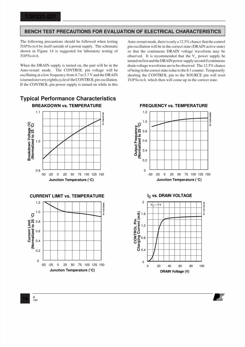
The following precautions should be followed when testing
TOPSwitch by itself outside of a power supply. The schematic
shown in Figure 14 is suggested for laboratory testing of
TOPSwitch.
When the DRAIN supply is turned on, the part will be in the
Auto-restart mode. The CONTROL pin voltage will be
oscillating at a low frequency from 4.7 to 5.7 V and the DRAIN
is turned on every eighth cycle of the CONTROL pin oscillation.
If the CONTROL pin power supply is turned on while in this
BENCH TEST PRECAUTIONS FOR EVALUATION OF ELECTRICAL CHARACTERISTICS
Typical Performance Characteristics
Auto-restart mode, there is only a 12.5% chance that the control
pin oscillation will be in the correct state (DRAIN active state)
so that the continuous DRAIN voltage waveform may be
observed. It is recommended that the VC
power supply be
turned on first and the DRAIN power supply second if continuousdrain voltage waveforms are to be observed. The 12.5% chance
of being in the correct state is due to the 8:1 counter. Temporarily
shorting the CONTROL pin to the SOURCE pin will reset
TOPSwitch, which then will come up in the correct state.
2
1.2
1.6
0
0 20 40 60 80 100
DRAIN Voltage (V)
C
O N T R O L P i n
C h a r g i n g C u r r e n t ( m A )
IC vs. DRAIN VOLTAGE
P I - 1 1 4 5 - 1 0 3 1 9 4
0.4
0.8
VC = 5 V
1.1
1.0
0.9-50 -25 0 25 50 75 100 125 150
Junction Temperature (°C)
B r e a k d o w n V o l t a g e ( V )
( N o r m a l i z e d t o 2 5 ° C )
BREAKDOWN vs. TEMPERATURE
P I - 1 7
6 B - 0 5 1 3 9 1
1.2
1.0
0.8
0.6
0.4
0.2
0-50 -25 0 25 50 75 100 125 150
Junction Temperature (°C)
CURRENT LIMIT vs. TEMPERATURE
P I - 1 1 2 5 - 0 3 3 0 0 1
C u r r e n t L i m i t
( N o r m a l i z e d t o 2 5 ° C )
1.2
1.0
0.8
0.6
0.4
0.2
0-50 -25 0 25 50 75 100 125 150
Junction Temperature (°C)
FREQUENCY vs. TEMPERATURE
P I - 1 1 2
3 A - 0 3 3 0 0 1
O u t p u t F r e q u e n c y
( N o r m a l i z e d t o 2 5 ° C )

8/2/2019 Top222g Pulse-width Modulation Switch
http://slidepdf.com/reader/full/top222g-pulse-width-modulation-switch 17/20

8/2/2019 Top222g Pulse-width Modulation Switch
http://slidepdf.com/reader/full/top222g-pulse-width-modulation-switch 18/20
TOP221-227
D
7/0118
B K
F
G
C
J
L
M
E
A
D
DIM
A
B
C
D
E
F
G
H
J
K
L
M
N
O
P
PI-1848-040901
inches
.460-.480
.400-.415
.236-.260
.240 - REF.
.520-.560
.028-.038
.045-.055
.090-.110
.165-.185
.045-.055
.095-.115
.015-.020
.705-.715
.146-.156
.103-.113
mm
11.68-12.19
10.16-10.54
5.99-6.60
6.10 - REF.
13.21-14.22
.71-.97
1.14-1.40
2.29-2.79
4.19-4.70
1.14-1.40
2.41-2.92
.38-.51
17.91-18.16
3.71-3.96
2.62-2.87
H
N
O
PNotes:1. Package dimensions conform toJEDEC specification TO-220 AB forstandard flange mounted, peripherallead package; .100 inch lead spacing(Plastic) 3 leads (issue J, March 1987)2. Controlling dimensions are inches.3. Pin numbers start with Pin 1, andcontinue from left to right whenviewed from the top.4. Dimensions shown do not includemold flash or other protrusions. Moldflash or protrusions shall not exceed.006 (.15 mm) on any side.5. Position of terminals to bemeasured at a position .25 (6.35 mm)from the body.6. All terminals are solder plated.
Y03A
TO-220/3
PI-2076-040901
1
A
K
J1
4
L
G
8 5
C
N
P08A
DIP-8
D S .004 (.10)
J2
-E-
-D-
B
-F-
DIM
A
B
C
G
H
J1
J2
K
L
M
N
P
Q
inches
0.370-0.385
0.245-0.255
0.125-0.135
0.015-0.040
0.120-0.135
0.060 (NOM)
0.014-0.022
0.010-0.012
0.090-0.110
0.030 (MIN)
0.300-0.320
0.300-0.390
0.300 BSC
mm
9.40-9.78
6.22-6.48
3.18-3.43
0.38-1.02
3.05-3.43
1.52 (NOM)
0.36-0.56
0.25-0.30
2.29-2.79
0.76 (MIN)
7.62-8.13
7.62-9.91
7.62 BSC
Notes:1. Package dimensions conform to JEDECspecification MS-001-AB for standard dualin-line (DIP) package .300 inch row spacing(PLASTIC) 8 leads (issue B, 7/85)..2. Controlling dimensions are inches.3. Dimensions shown do not include moldflash or other protrusions. Mold flash orprotrusions shall not exceed .006 (.15) onany side.4. D, E and F are reference datums on themolded body.
H
M
P
Q
8/2/2019 Top222g Pulse-width Modulation Switch
http://slidepdf.com/reader/full/top222g-pulse-width-modulation-switch 19/20
TOP221-227
D
7/01 19
PI-2077-042601
1
A
J1
4
L
8 5
C
G08A
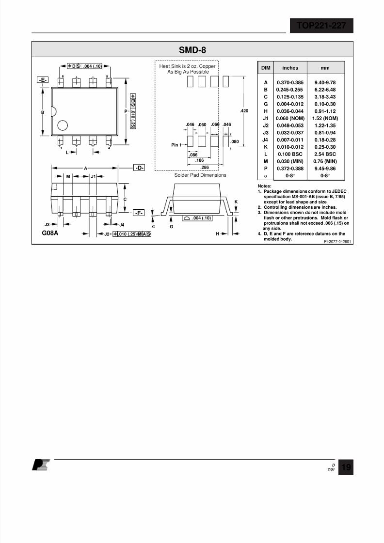
SMD-8
D S .004 (.10)
J2
E
S
. 0 1 0 ( .2 5 )
-E-
-D-
B
-F-
M
J3
DIM
A
B
C
G
H
J1
J2
J3
J4
K
L
M
P
α
inches
0.370-0.385
0.245-0.255
0.125-0.135
0.004-0.012
0.036-0.044
0.060 (NOM)
0.048-0.053
0.032-0.037
0.007-0.011
0.010-0.012
0.100 BSC
0.030 (MIN)
0.372-0.388
0-8°
mm
9.40-9.78
6.22-6.48
3.18-3.43
0.10-0.30
0.91-1.12
1.52 (NOM)
1.22-1.35
0.81-0.94
0.18-0.28
0.25-0.30
2.54 BSC
0.76 (MIN)
9.45-9.86
0-8°
Notes:
1. Package dimensions conform to JEDECspecification MS-001-AB (issue B, 7/85)
except for lead shape and size.
2. Controlling dimensions are inches.3. Dimensions shown do not include mold
flash or other protrusions. Mold flash or
protrusions shall not exceed .006 (.15) onany side.
4. D, E and F are reference datums on the
molded body.
K
Gα
H
.004 (.10)
J4
P
.010 (.25) M A S
Heat Sink is 2 oz. CopperAs Big As Possible
.420
.046 .060 .060 .046
.080Pin 1
.086
.186
.286
Solder Pad Dimensions

8/2/2019 Top222g Pulse-width Modulation Switch
http://slidepdf.com/reader/full/top222g-pulse-width-modulation-switch 20/20
TOP221-227
D
Notes
-
1) Updated package references.
2) Corrected Spelling.
3) Corrected Storage Temperature θJC
and updated nomenclature in parameter table.
4) Added G package references to Self-Protection Current Limit parameter.5) Corrected font sizes in figures.
Date
12/97
7/01
Revision
C
D
KOREA
Power Integrations
International Holdings, Inc.
Rm# 402, Handuk Building
649-4 Yeoksam-Dong,
Kangnam-Gu,
Seoul, Korea
Phone: +82-2-568-7520
Fax: +82-2-568-7474
e-mail: [email protected]
WORLD HEADQUARTERS
AMERICAS
Power Integrations, Inc.
5245 Hellyer Avenue
San Jose, CA 95138 USA
Main: +1 408-414-9200
Customer Service:
Phone: +1 408-414-9665
Fax: +1 408-414-9765
e-mail: [email protected]
For the latest updates, visit our Web site: www.powerint.com
Power Integrations reserves the right to make changes to its products at any time to improve reliability or manufacturability.
Power Integrations does not assume any liability arising from the use of any device or circuit described herein, nor does it
convey any license under its patent rights or the rights of others.
The PI Logo, TOPSwitch , TinySwitch and EcoSmart are registered trademarks of Power Integrations, Inc.
©Copyright 2001, Power Integrations, Inc.
JAPAN
Power Integrations, K.K.
Keihin-Tatemono 1st Bldg.
12-20 Shin-Yokohama 2-Chome
Kohoku-ku, Yokohama-shi
Kanagawa 222-0033, Japan
Phone: +81-45-471-1021
Fax: +81-45-471-3717
e-mail: [email protected]
TAIWAN
Power Integrations
International Holdings, Inc.
17F-3, No. 510
Chung Hsiao E. Rd.,
Sec. 5,
Taipei, Taiwan 110, R.O.C.
Phone: +886-2-2727-1221
Fax: +886-2-2727-1223
e-mail: [email protected]
EUROPE & AFRICA
Power Integrations (Europe) Ltd.
Centennial Court
Easthampstead Road
Bracknell
Berkshire, RG12 1YQ
United Kingdom
Phone: +44-1344-462-300
Fax: +44-1344-311-732
e-mail: [email protected]
CHINA
Power Integrations
International Holdings, Inc.
Rm# 1705, Bao Hua Bldg.
1016 Hua Qiang Bei Lu
Shenzhen, Guangdong 518031
China
Phone: +86-755-367-5143
Fax: +86-755-377-9610
e-mail: [email protected]
INDIA (Technical Support)
Innovatech
#1, 8th Main Road
Vasanthnagar
Bangalore, India 560052
Phone: +91-80-226-6023
Fax: +91-80-228-9727
e-mail: [email protected]
APPLICATIONS HOTLINE
World Wide +1-408-414-9660
APPLICATIONS FAX
World Wide +1-408-414-9760
Related Documents