Three-port DC-DC Converters to Interface Renewable Energy Sources with Bi-directional Load and Energy Storage Ports A DISSERTATION SUBMITTED TO THE FACULTY OF THE GRADUATE SCHOOL OF THE UNIVERSITY OF MINNESOTA BY Hariharan Krishnaswami IN PARTIAL FULFILLMENT OF THE REQUIREMENTS FOR THE DEGREE OF DOCTOR OF PHILOSOPHY August, 2009

Welcome message from author
This document is posted to help you gain knowledge. Please leave a comment to let me know what you think about it! Share it to your friends and learn new things together.
Transcript
Three-port DC-DC Converters to Interface Renewable
Energy Sources with Bi-directional Load and Energy
Storage Ports
A DISSERTATION
SUBMITTED TO THE FACULTY OF THE GRADUATE SCHOOL
OF THE UNIVERSITY OF MINNESOTA
BY
Hariharan Krishnaswami
IN PARTIAL FULFILLMENT OF THE REQUIREMENTS
FOR THE DEGREE OF
DOCTOR OF PHILOSOPHY
August, 2009

c© Hariharan Krishnaswami 2009

Acknowledgements
It is a pleasure to thank the many people who have made this thesis possible.
I owe my deepest gratitude to my supervisor, Professor Mohan, who has guided,
mentored and supported me throughout my graduate studies. This thesis would not
have been possible without his valuable inputs, good teaching and sound advice. He
has always been and will be an inspiration to me.
I would like to thank Professor Robbins for providing me an opportunity to teach
and gain valuable teaching experience. I would like to thank Professor Wollenberg
for his excellent teaching and continuous encouragement. I am grateful to Professor
Imbertson for his guidance during my job as a teaching assistant. I would also like to
thank Professor Rajamani for having agreed to be part of the oral exam committee. I
owe my gratitude to all the Professors who have taught me in graduate school.
I gratefully acknowledge the support given by Institute of Renewable Energy and
Environment, University of Minnesota for this dissertation.
I would like to thank my parents who have given me unfailing support and love
throughout and to whom I have dedicated this thesis. I would also like to thank my
family members and relatives who have inspired and continuously motivated me.
My stay in graduate school has been made memorable by my friends, Ranjan,
Apurva, Kaushik and Shivaraj with whom I had countless technical and personal dis-
cussions. I would also like to thank all my lab colleagues for creating a learning and fun
environment.
i

Dedication
To my parents
ii

ABSTRACT
Power electronic converters are needed to interface multiple renewable energy sources
with the load along with energy storage in stand-alone or grid-connected residential,
commercial and automobile applications. Recently, multi-port converters have attracted
attention for such applications since they use single-stage high frequency ac-link based
power conversion as compared to several power conversion stages in conventional dc-link
based systems. In this thesis, two high frequency ac-link topologies are proposed, series
resonant and current-fed three-port dc-dc converters. A renewable energy source such
as fuel-cell or PV array can be connected to one of the ports, batteries or other types
of energy storage devices to the second port and the load to the third port.
The series resonant three-port converter has two series-resonant tanks, a three-
winding transformer and three active full-bridges with phase-shift control between them.
The converter has capabilities of bi-directional power flow in the battery and the load
port. Use of series-resonance aids in high switching frequency operation with realizable
component values when compared to existing three-port converter with only induc-
tors. Steady-state analysis of the converter is presented to determine the power flow
equations, tank currents and soft-switching operation boundary. Dynamic analysis is
performed to design a closed-loop controller to regulate the load-side port voltage and
source-side port current. Design procedure for the three-port converter is explained and
experimental results of a laboratory prototype are presented.
For applications where the load-port is not regenerative, a diode bridge is more
economical than an active bridge at the load-side port. For this configuration, to con-
trol the output voltage and to share the power between the two sources, two control
variables are proposed. One of them is the phase shift between the outputs of the
active bridges and the other between two legs in one of the bridges. The latter uses
phase-shift modulation to reduce the value of the fundamental of the bridge output.
Steady-state analysis is presented to determine the output voltage, input port power
and soft-switching operation boundary as a function of the phase shifts. It is observed
from the analysis that the power can be made bi-directional in either of the source ports
iii

by varying the phase shifts. Design procedure, simulation and experimental results of
a prototype converter are presented.
The current-fed bi-directional three-port converter consists of three active full bridges
with phase-shift control between them. Their inputs are connected to dc voltage ports
through series inductors and hence termed as current-fed. The outputs are connected
to three separate transformers whose secondary are configured in delta, with high fre-
quency capacitors in parallel to each transformer secondary. The converter can be used
in applications where dc currents at the ports and high step-up voltage ratios are de-
sired. Steady-state analysis to determine power flow equations and dynamic analysis
are presented. The output voltage is independent of the load as observed from analysis.
Simulation results are presented to verify the analysis.
iv

Contents
Acknowledgements i
Dedication ii
Abstract iii
List of Tables ix
List of Figures x
1 Introduction 1
1.1 Multi-port dc-dc converter . . . . . . . . . . . . . . . . . . . . . . . . . . 1
1.1.1 Characteristics of multi-port converter . . . . . . . . . . . . . . . 1
1.1.2 Applications of multi-port dc-dc converter . . . . . . . . . . . . . 2
1.1.3 High frequency ac-link based multi-port converter . . . . . . . . 3
1.2 Existing three-port converter circuits . . . . . . . . . . . . . . . . . . . . 6
1.2.1 Triple active bridge three-port bi-directional converter . . . . . . 6
1.2.2 Triple half-bridge bi-directional converter . . . . . . . . . . . . . 7
1.2.3 Multiple-input buck-boost converter . . . . . . . . . . . . . . . . 8
1.3 Scope of this thesis . . . . . . . . . . . . . . . . . . . . . . . . . . . . . . 9
1.4 Contributions of this thesis . . . . . . . . . . . . . . . . . . . . . . . . . 10
1.5 Organization of this thesis . . . . . . . . . . . . . . . . . . . . . . . . . . 10
1.6 Conclusion . . . . . . . . . . . . . . . . . . . . . . . . . . . . . . . . . . 11
v

2 Three-port Series Resonant Converter - Steady-state Analysis 12
2.1 Principle of operation . . . . . . . . . . . . . . . . . . . . . . . . . . . . 12
2.1.1 Two-port series resonant converter . . . . . . . . . . . . . . . . . 12
2.1.2 Three-port series resonant converter . . . . . . . . . . . . . . . . 14
2.1.3 Analysis of port voltages and currents . . . . . . . . . . . . . . . 15
2.2 Steady-state power flow equations . . . . . . . . . . . . . . . . . . . . . 17
2.3 Soft-switching operation boundary . . . . . . . . . . . . . . . . . . . . . 18
2.4 Peak currents in tank circuit . . . . . . . . . . . . . . . . . . . . . . . . 20
2.5 Three-winding transformer model . . . . . . . . . . . . . . . . . . . . . . 21
2.5.1 Modeling of three-winding transformer . . . . . . . . . . . . . . . 22
2.5.2 Modeling of transformer with resonant circuit elements . . . . . 23
2.6 Conclusion . . . . . . . . . . . . . . . . . . . . . . . . . . . . . . . . . . 25
3 Three-port Series Resonant Converter - Dynamic Analysis 26
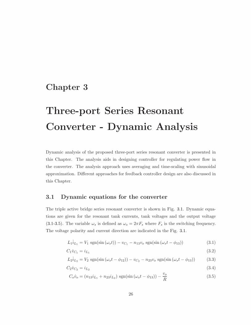
3.1 Dynamic equations for the converter . . . . . . . . . . . . . . . . . . . . 26
3.2 Averaged model of three-port series resonant converter . . . . . . . . . . 27
3.2.1 Generalized averaging method . . . . . . . . . . . . . . . . . . . 28
3.2.2 Application to three-port converter . . . . . . . . . . . . . . . . . 28
3.3 Normalization of the state equations . . . . . . . . . . . . . . . . . . . . 31
3.3.1 Steady-state results using averaged model . . . . . . . . . . . . . 32
3.4 Time-Scaling for the dynamic system . . . . . . . . . . . . . . . . . . . . 32
3.5 Controller design . . . . . . . . . . . . . . . . . . . . . . . . . . . . . . . 33
3.6 Conclusion . . . . . . . . . . . . . . . . . . . . . . . . . . . . . . . . . . 35
4 Three-port Series Resonant Converter - Design and Results 36
4.1 Design requirements . . . . . . . . . . . . . . . . . . . . . . . . . . . . . 36
4.2 Design procedure . . . . . . . . . . . . . . . . . . . . . . . . . . . . . . . 37
4.2.1 Prototype specifications . . . . . . . . . . . . . . . . . . . . . . . 37
4.2.2 Resonant converter parameters . . . . . . . . . . . . . . . . . . . 38
4.2.3 Transformer design . . . . . . . . . . . . . . . . . . . . . . . . . . 40
4.3 Simulation results . . . . . . . . . . . . . . . . . . . . . . . . . . . . . . 41
4.3.1 Simulations results at different operating points . . . . . . . . . . 42
4.3.2 Closed loop controller simulation . . . . . . . . . . . . . . . . . . 46
vi

4.4 Experimental results . . . . . . . . . . . . . . . . . . . . . . . . . . . . . 48
4.4.1 Laboratory setup . . . . . . . . . . . . . . . . . . . . . . . . . . . 48
4.4.2 Prototype results . . . . . . . . . . . . . . . . . . . . . . . . . . . 49
4.5 Comparison with existing three-port converter . . . . . . . . . . . . . . 52
4.5.1 Comparison at constant switching frequency . . . . . . . . . . . . 54
4.5.2 Comparison at constant voltage ratios . . . . . . . . . . . . . . . 58
4.5.3 Comparison based on magnetizing inductance . . . . . . . . . . . 58
4.5.4 Comparison conclusion . . . . . . . . . . . . . . . . . . . . . . . . 59
4.6 Conclusion . . . . . . . . . . . . . . . . . . . . . . . . . . . . . . . . . . 59
5 Three-port Series Resonant Converter - Load-side Diode Bridge 60
5.1 Proposed topology and modulation schemes . . . . . . . . . . . . . . . . 60
5.2 Steady-state analysis . . . . . . . . . . . . . . . . . . . . . . . . . . . . . 62
5.2.1 Equivalent circuit . . . . . . . . . . . . . . . . . . . . . . . . . . . 62
5.2.2 Steady-state equations . . . . . . . . . . . . . . . . . . . . . . . . 63
5.2.3 Plots of output voltage and port power . . . . . . . . . . . . . . 65
5.2.4 Peak tank currents . . . . . . . . . . . . . . . . . . . . . . . . . . 67
5.2.5 Soft-switching operation . . . . . . . . . . . . . . . . . . . . . . . 67
5.3 Design Procedure . . . . . . . . . . . . . . . . . . . . . . . . . . . . . . . 69
5.4 Simulation results . . . . . . . . . . . . . . . . . . . . . . . . . . . . . . 71
5.4.1 Simulation method . . . . . . . . . . . . . . . . . . . . . . . . . . 71
5.4.2 Simulation results at different operating points . . . . . . . . . . 72
5.4.3 Component specifications . . . . . . . . . . . . . . . . . . . . . . 75
5.5 Experimental results . . . . . . . . . . . . . . . . . . . . . . . . . . . . . 81
5.5.1 Experimental setup . . . . . . . . . . . . . . . . . . . . . . . . . . 81
5.5.2 Prototype results . . . . . . . . . . . . . . . . . . . . . . . . . . . 82
5.6 Conclusion . . . . . . . . . . . . . . . . . . . . . . . . . . . . . . . . . . 85
6 Current-fed Three-port Converter 88
6.1 Introduction . . . . . . . . . . . . . . . . . . . . . . . . . . . . . . . . . . 88
6.2 Proposed three-port converter . . . . . . . . . . . . . . . . . . . . . . . . 90
6.3 Steady-state analysis . . . . . . . . . . . . . . . . . . . . . . . . . . . . . 92
6.4 Dynamic analysis . . . . . . . . . . . . . . . . . . . . . . . . . . . . . . . 100
vii

6.4.1 State-space representation of the converter . . . . . . . . . . . . 100
6.4.2 Averaging . . . . . . . . . . . . . . . . . . . . . . . . . . . . . . . 101
6.5 Results . . . . . . . . . . . . . . . . . . . . . . . . . . . . . . . . . . . . . 103
6.5.1 Simulation results . . . . . . . . . . . . . . . . . . . . . . . . . . 103
6.5.2 Experimental results . . . . . . . . . . . . . . . . . . . . . . . . . 107
6.6 Conclusion . . . . . . . . . . . . . . . . . . . . . . . . . . . . . . . . . . 110
7 Conclusion 111
7.1 Conclusion . . . . . . . . . . . . . . . . . . . . . . . . . . . . . . . . . . 111
7.1.1 Series resonant three-port converter . . . . . . . . . . . . . . . . 111
7.1.2 Current-fed three-port converter . . . . . . . . . . . . . . . . . . 113
7.2 Future work . . . . . . . . . . . . . . . . . . . . . . . . . . . . . . . . . . 114
Bibliography 115
viii

List of Tables
4.1 Converter specifications . . . . . . . . . . . . . . . . . . . . . . . . . . . 38
4.2 Three-port converter parameters . . . . . . . . . . . . . . . . . . . . . . 39
4.3 Three-winding transformer prototype details . . . . . . . . . . . . . . . . 40
4.4 Converter specifications for comparison between TAB and TABSRC . . 56
4.5 Converter parameters TAB, TABSRC at constant switching frequency . 57
4.6 TAB vs TABSRC at constant switching frequency . . . . . . . . . . . . 57
4.7 Converter parameters for TAB, TABSRC for constant voltage ratios . . 58
4.8 TAB vs TABSRC at constant voltage ratios . . . . . . . . . . . . . . . . 59
5.1 Parameters for load-side diode bridge converter . . . . . . . . . . . . . . 71
5.2 Sinusoidal approximation vs exact model . . . . . . . . . . . . . . . . . . 75
5.3 Soft-switching range at various loads . . . . . . . . . . . . . . . . . . . . 78
5.4 Summary of simulation results . . . . . . . . . . . . . . . . . . . . . . . 81
6.1 Current-fed three-port converter specifications . . . . . . . . . . . . . . . 96
6.2 Current-fed three-port converter parameters . . . . . . . . . . . . . . . . 97
ix

List of Figures
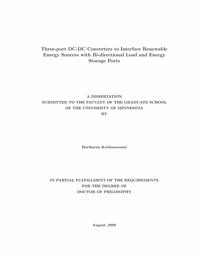
1.1 Block diagram of multi-port dc-dc converter . . . . . . . . . . . . . . . . 2
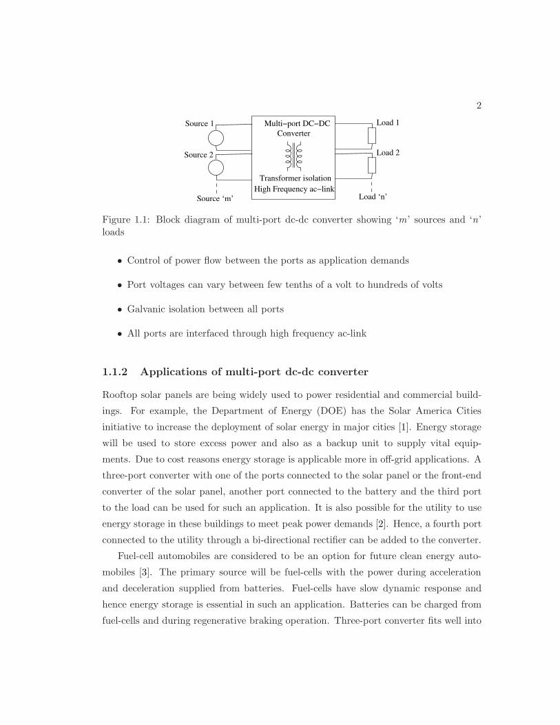
1.2 Block diagram of three-port dc-dc converter with dc link . . . . . . . . . 4
1.3 Block diagram of three-port dc-dc converter with high frequency ac-link 4
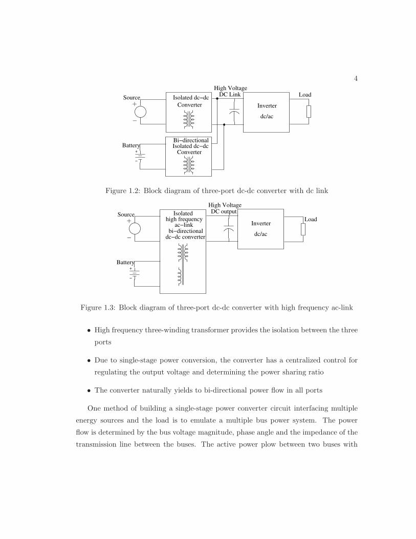
1.4 Triple active bridge three-port bi-directional converter . . . . . . . . . . 6
1.5 Three-winding transformer model equivalent representation . . . . . . . 7
1.6 Triple half-bridge bi-directional converter . . . . . . . . . . . . . . . . . 8
1.7 Multiple-input buck-boost converter . . . . . . . . . . . . . . . . . . . . 9
2.1 Two-port series resonant converter with two active bridges . . . . . . . . 13
2.2 Proposed three-port series resonant converter circuit . . . . . . . . . . . 14
2.3 Converter voltage and current waveforms . . . . . . . . . . . . . . . . . 15
2.4 Plot of output voltage vs phase-shift . . . . . . . . . . . . . . . . . . . . 17
2.5 Plot of port power vs phase-shift . . . . . . . . . . . . . . . . . . . . . . 19
2.6 Port3 soft-switching operation boundary . . . . . . . . . . . . . . . . . . 20
2.7 Port2 peak normalized tank current . . . . . . . . . . . . . . . . . . . . 21
2.8 Three-winding transformer T-model . . . . . . . . . . . . . . . . . . . . 22
2.9 Three-winding transformer π-model . . . . . . . . . . . . . . . . . . . . 22
3.1 Three-port series resonant circuit for dynamic analysis . . . . . . . . . . 27
3.2 Block diagram for controlling the three-port converter . . . . . . . . . . 34
4.1 Operating region for the converter . . . . . . . . . . . . . . . . . . . . . 37
4.2 Calculated phase-shifts along the boundary of operating region . . . . . 40
4.3 Effect of leakage inductance on phase-shifts . . . . . . . . . . . . . . . . 41
4.4 Simulated port waveforms at operating point B . . . . . . . . . . . . . . 42
4.5 Simulated port input currents at operating point B . . . . . . . . . . . . 42
4.6 Simulated port waveforms at operating point C . . . . . . . . . . . . . . 43
x

4.7 Simulated port input currents at operating point C . . . . . . . . . . . . 43
4.8 Simulated port waveforms at operating point D . . . . . . . . . . . . . . 44
4.9 Simulated port input currents at operating point D . . . . . . . . . . . . 44
4.10 Simulated output waveforms in region3 . . . . . . . . . . . . . . . . . . . 45
4.11 Simulated port waveforms in region3 . . . . . . . . . . . . . . . . . . . . 45
4.12 Output voltage response with PI controller . . . . . . . . . . . . . . . . 46
4.13 Port current responses with PI controller . . . . . . . . . . . . . . . . . 46
4.14 Output voltage response with nonlinear controller . . . . . . . . . . . . . 47
4.15 Port current responses with non-linear controller . . . . . . . . . . . . . 47
4.16 Carrier signal and control voltages for PWM . . . . . . . . . . . . . . . 48
4.17 Hardware setup . . . . . . . . . . . . . . . . . . . . . . . . . . . . . . . . 49
4.18 Port1 waveforms at operating point B . . . . . . . . . . . . . . . . . . . 50
4.19 Port2 waveforms at operating point B . . . . . . . . . . . . . . . . . . . 50
4.20 Port3 waveforms at operating point B . . . . . . . . . . . . . . . . . . . 51
4.21 Port1 and port2 high frequency voltage waveforms for B . . . . . . . . . 51
4.22 Port2 dc waveforms at operating point C . . . . . . . . . . . . . . . . . 52
4.23 Port3 waveforms around operating point C . . . . . . . . . . . . . . . . 52
4.24 Port1 high frequency waveforms at operating point C . . . . . . . . . . . 53
4.25 Port2 high frequency waveforms around operating point C . . . . . . . . 53
4.26 Port2 dc waveforms at operating point D . . . . . . . . . . . . . . . . . 54
4.27 Port1 and port2 high frequency voltage waveforms for D . . . . . . . . . 54
4.28 Port2 high frequency waveforms at operating point D . . . . . . . . . . 55
4.29 Port3 high frequency waveforms at operating point D . . . . . . . . . . 55
4.30 Dynamic response for a step change in load . . . . . . . . . . . . . . . . 56
5.1 Three-port series resonant converter with diode bridge . . . . . . . . . . 61
5.2 Bridge voltage waveforms v1hf , v2hf showing definitions of θ and φ . . . 62
5.3 AC equivalent circuit for analysis . . . . . . . . . . . . . . . . . . . . . . 63
5.4 Plot of output voltage vs phase-shift angle . . . . . . . . . . . . . . . . . 65
5.5 Plot of port power vs phase-shift angle . . . . . . . . . . . . . . . . . . . 66
5.6 Output voltage comparison between two converters . . . . . . . . . . . . 67
5.7 Plot of normalized peak tank currents . . . . . . . . . . . . . . . . . . . 68
5.8 Plot of soft-switching operation region . . . . . . . . . . . . . . . . . . . 69
xi

5.9 Operating region of converter . . . . . . . . . . . . . . . . . . . . . . . . 70
5.10 Simulated port voltages and tank currents for operating point B . . . . 72
5.11 Simulated input port currents for operating point C . . . . . . . . . . . 72
5.12 Simulated port voltages and tank currents for operating point C . . . . 73
5.13 Simulated input port currents for operating point C . . . . . . . . . . . 73
5.14 Simulated port voltages and tank currents for operating point D . . . . 74
5.15 Simulated input port currents for operating point D . . . . . . . . . . . 74
5.16 Simulation results of peak tank currents . . . . . . . . . . . . . . . . . . 76
5.17 Simulation results of peak tank voltages . . . . . . . . . . . . . . . . . . 77
5.18 Simulation results of output voltage . . . . . . . . . . . . . . . . . . . . 78
5.19 Simulation results to indicate soft-switching operation range . . . . . . . 79
5.20 Simulation results of filter currents . . . . . . . . . . . . . . . . . . . . . 80
5.21 Hardware setup for testing . . . . . . . . . . . . . . . . . . . . . . . . . . 82
5.22 Observed waveforms for operating point B . . . . . . . . . . . . . . . . . 83
5.23 Observed waveforms for operating point B (contd.) . . . . . . . . . . . . 83
5.24 Observed waveforms for operating point B (contd.) . . . . . . . . . . . . 84
5.25 Observed waveforms for operating point B (contd.) . . . . . . . . . . . . 84
5.26 Observed waveforms for operating point C . . . . . . . . . . . . . . . . . 85
5.27 Observed waveforms for operating point C (contd.) . . . . . . . . . . . . 85
5.28 Observed waveforms for operating point D . . . . . . . . . . . . . . . . . 86
5.29 Observed waveforms for operating point D (contd.) . . . . . . . . . . . . 86
5.30 Observed waveforms for operating point D (contd.) . . . . . . . . . . . . 87
6.1 Existing dual active bridge converter . . . . . . . . . . . . . . . . . . . . 89
6.2 Existing inverse dual converter . . . . . . . . . . . . . . . . . . . . . . . 89
6.3 Waveforms of inverse dual converter . . . . . . . . . . . . . . . . . . . . 90
6.4 Proposed current-fed three-port converter . . . . . . . . . . . . . . . . . 91
6.5 Bi-directional switch for battery port . . . . . . . . . . . . . . . . . . . . 91
6.6 Waveforms indicating phase-shifts and capacitor voltages . . . . . . . . 93
6.7 Equivalent circuit for steady-state analysis . . . . . . . . . . . . . . . . . 94
6.8 Output voltage waveforms vs phase-shift angles . . . . . . . . . . . . . . 98
6.9 Port power vs phase-shift angles at full load . . . . . . . . . . . . . . . . 99
6.10 Port power vs phase-shift angles at full load . . . . . . . . . . . . . . . . 100
xii

6.11 Simulated winding currents - equal load sharing mode . . . . . . . . . . 103
6.12 Simulated capacitor voltages - equal load sharing mode . . . . . . . . . 103
6.13 Simulated port power - equal load sharing mode . . . . . . . . . . . . . 104
6.14 Simulated winding currents - battery charging mode . . . . . . . . . . . 104
6.15 Simulated capacitor voltages - battery charging mode . . . . . . . . . . 105
6.16 Simulated port power - battery charging mode . . . . . . . . . . . . . . 105
6.17 Response in open loop for a step change in load . . . . . . . . . . . . . . 106
6.18 Response in closed loop for a step change in load . . . . . . . . . . . . . 107
6.19 Observed capacitor voltages - power sharing mode . . . . . . . . . . . . 108
6.20 Observed square-wave currents - power sharing mode . . . . . . . . . . . 108
6.21 Observed transformer winding3 voltage . . . . . . . . . . . . . . . . . . 109
6.22 Observed capacitor voltages - power sharing mode (contd.) . . . . . . . 109
xiii

Chapter 1
Introduction
Renewable energy sources such as Fuel-Cells, Photo-Voltaic (PV) arrays are increas-
ingly being used in automobiles, residential and commercial buildings. For stand-alone
systems energy storage devices are required for backup power and fast dynamic re-
sponse. A power electronic converter interfaces the sources with the load along with
energy storage. Existing converters for such applications use a common dc-link. High
frequency ac-link based systems have recently been explored due to its advantages of
reduced part count, reduced size and centralized control. Such a high frequency ac-link
based converter is termed as a multi-port converter in literature, to whose ports are
connected the energy sources, energy storage devices and the load. In this chapter an
introduction to multi-port converter is given. This is followed by the context, scope,
contributions and organization of this thesis.
1.1 Multi-port dc-dc converter
1.1.1 Characteristics of multi-port converter
Multi-port converter has several ports to which sources or loads can be connected as
shown in Fig. 1.1. The converter regulates the power flow between the sources and the
loads. All of the ports have bi-directional power flow capability. The characteristics of
a multi-port converter are,
• Bi-directional power flow in all of the ports
1
2
Source 2
Multi−port DC−DC
Converter
Source ‘m’
Load 1
Load 2
Load ‘n’
Transformer isolation
High Frequency ac−link
Source 1
Figure 1.1: Block diagram of multi-port dc-dc converter showing ‘m’ sources and ‘n’loads
• Control of power flow between the ports as application demands
• Port voltages can vary between few tenths of a volt to hundreds of volts
• Galvanic isolation between all ports
• All ports are interfaced through high frequency ac-link
1.1.2 Applications of multi-port dc-dc converter
Rooftop solar panels are being widely used to power residential and commercial build-
ings. For example, the Department of Energy (DOE) has the Solar America Cities
initiative to increase the deployment of solar energy in major cities [1]. Energy storage
will be used to store excess power and also as a backup unit to supply vital equip-
ments. Due to cost reasons energy storage is applicable more in off-grid applications. A
three-port converter with one of the ports connected to the solar panel or the front-end
converter of the solar panel, another port connected to the battery and the third port
to the load can be used for such an application. It is also possible for the utility to use
energy storage in these buildings to meet peak power demands [2]. Hence, a fourth port
connected to the utility through a bi-directional rectifier can be added to the converter.
Fuel-cell automobiles are considered to be an option for future clean energy auto-
mobiles [3]. The primary source will be fuel-cells with the power during acceleration
and deceleration supplied from batteries. Fuel-cells have slow dynamic response and
hence energy storage is essential in such an application. Batteries can be charged from
fuel-cells and during regenerative braking operation. Three-port converter fits well into

3
this fuel-cell vehicle application. An uninterruptible power supply (UPS) can also be
considered as a three-port converter [4]
The three-port converter discussed in this thesis has dc ports. If a motor or residen-
tial load needs ac, an inverter can be connected at the output of the load port. Some
applications where multi-port converter can be used are listed below.
1. Fuel-cell hybrid automobiles – Port1: Fuel-cell, Port2: Batteries and/or ultraca-
pacitors and Port3: Automobile load - Electric drive
2. Fuel-cell power conditioning systems – Port1: Fuel-cell, Port2: Batteries and
Port3: AC loads with three-phase inverter
3. Off-grid residential buildings – Port1: Solar panels or Fuel-cells, Port2: Batteries
and Port3: Residential loads
4. Grid-connected residential buildings – Port1: Solar panels or Fuel-cells, Port2:
Batteries, Port3: Utility and Port4: Residential loads
1.1.3 High frequency ac-link based multi-port converter
Existing converter for the applications mentioned in the previous section use a common
high voltage dc link as shown in Fig. 1.2. There are two stages of conversion, a dc-
dc converter between the source and the dc bus and a bi-directional dc-dc converter
between the battery and the dc bus. The load is connected to the dc bus through
an inverter. Each of the dc-dc converters have a separate control stage along with a
centralized control for determining power sharing ratio.
The dc link in Fig. 1.2 can be replaced with high frequency ac link and the number
of stages can be reduced from two to one. Such a three-port converter is shown in Fig
1.3. The advantages of such an approach are [5],
• Single power conversion stage reduces component count on semiconductor switches,
drive circuits and magnetics
• Reduced size due to reduced component count when compared to dc link based
three-port converter
4
Converter
Battery
SourceDC Link
High Voltage
Isolated dc−dc
Inverter
dc/ac
Load
Bi−directionalIsolated dc−dc
Converter
−
+
−
+
Figure 1.2: Block diagram of three-port dc-dc converter with dc link
bi−directional
Source
Battery
High VoltageDC output
Inverter
dc/ac
LoadIsolated
high frequencyac−link
dc−dc converter
−
+
−
+
Figure 1.3: Block diagram of three-port dc-dc converter with high frequency ac-link
• High frequency three-winding transformer provides the isolation between the three
ports
• Due to single-stage power conversion, the converter has a centralized control for
regulating the output voltage and determining the power sharing ratio
• The converter naturally yields to bi-directional power flow in all ports
One method of building a single-stage power converter circuit interfacing multiple
energy sources and the load is to emulate a multiple bus power system. The power
flow is determined by the bus voltage magnitude, phase angle and the impedance of the
transmission line between the buses. The active power plow between two buses with

5
voltages V1∠0 and V2∠ − θ is given by (1.1).
P =V1V2
Xsin θ (1.1)
where P = Active power flow from bus1 to bus2
Vi = Voltage magnitude at bus ‘i’
θ = Phase angle difference in radians between bus1 and bus2 voltages
X = Transmission line reactance ωL
The bus voltages are generated from dc sources using power electronic converters
which can vary the magnitude, phase angle and the frequency of the bus voltages.
Hence power flow can be controlled by the phase angles or voltage magnitudes or the
frequency which changes the impedance or a combination of all these three methods.
The impedance can be an inductor, capacitor or a resonant circuit using different con-
nections of inductors and capacitors.
Two-port converter circuits using this principle of power flow such as the dual active
bridge converter [6] and series resonant converter [7] have been existing in literature.
These circuits are used in high-power dc-dc converters and high output voltage dc-dc
converters. Also these converters are predominantly used for uni-directional power flow
from source to load. Hence the load side active switches are replaced by a diode bridge.
For telecommunication and aerospace applications high frequency ac-link based systems
were explored [8,9]. They have multiple power converters powered from the same source
or different sources, used mainly for paralleling operation and ac distribution.
With increased use of renewable energy sources in recent years, three-port or multi-
port configurations with bi-directional ports have gained attraction. The principle of
power flow explained using (1.1) can be extended for these applications. Several topolo-
gies and control methods have been proposed in literature. All of these topologies use
inductors as the main power transfer and storage element. The following section ex-
plains the existing three-port converters. Another method of building a single stage
power converter circuit is to use time-sharing principle i.e., at any time instant only
one of the sources will be connected to the load. This method is also explained in the
following section.
6
−−
+
+
−
+
−
+Cf1
Cf2
iL1
iL2
Port3
S3 S3
vohf
Co
S1 S1
v1hf
S2 S2
v2hf
Phase Shift φ12 Load port
Phase Shift φ13
Io
RPort1
Battery Port
V1
V2
i1lf
i2lf
Vo
iolf
S3S3
S2S2
S1S1
iohf
I1
I2
L1
L2n23 : 1
n13 : 1L3
Port2
Figure 1.4: Triple active bridge three-port bi-directional converter
1.2 Existing three-port converter circuits
1.2.1 Triple active bridge three-port bi-directional converter
A three-port bi-directional converter using the principle explained in Section 1.1.3 for
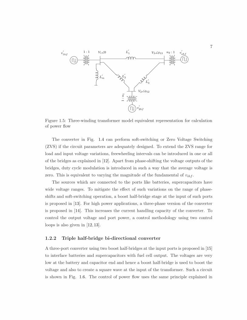
hybrid fuel-cell systems was proposed in [10]. The circuit diagram is shown in Fig.
1.4 where the full-bridges operate in square wave mode phase-shifted from each other.
The phase-shift angle is assumed to be positive when lagging. The transformer can be
represented as an extended cantilever model [11] as shown in Fig. 1.5 so that expressions
for power flow can be derived. One of the power flow equations is given in (1.2). Note
that the bus voltages are square waves. The converter proposed in [10] is a three-
port extension of the dual active bridge converter [6]. One of the drawbacks of this
converter is that the switching frequency and the inductor value cannot be determined
independently for the same power level in (1.2). The inductor Li includes the leakage
inductance of the transformer. To achieve realizable inductor values greater than or
equal to the leakage inductances of the transformer, the switching frequency should be
reduced.
P13 =V1V3
ωsL′
1
φ13
(
1 − |φ13|π
)
(1.2)
7
1:n
1
L′
1
L′
3
L′
2L′
m
v′
1hf
v′
2hf
1 : 1 v′
ohfn2 : 1V1∠0
V2∠φ12
V3∠φ13
Figure 1.5: Three-winding transformer model equivalent representation for calculationof power flow
The converter in Fig. 1.4 can perform soft-switching or Zero Voltage Switching
(ZVS) if the circuit parameters are adequately designed. To extend the ZVS range for
load and input voltage variations, freewheeling intervals can be introduced in one or all
of the bridges as explained in [12]. Apart from phase-shifting the voltage outputs of the
bridges, duty cycle modulation is introduced in such a way that the average voltage is
zero. This is equivalent to varying the magnitude of the fundamental of vihf .
The sources which are connected to the ports like batteries, supercapacitors have
wide voltage ranges. To mitigate the effect of such variations on the range of phase-
shifts and soft-switching operation, a boost half-bridge stage at the input of such ports
is proposed in [13]. For high power applications, a three-phase version of the converter
is proposed in [14]. This increases the current handling capacity of the converter. To
control the output voltage and port power, a control methodology using two control
loops is also given in [12,13].
1.2.2 Triple half-bridge bi-directional converter
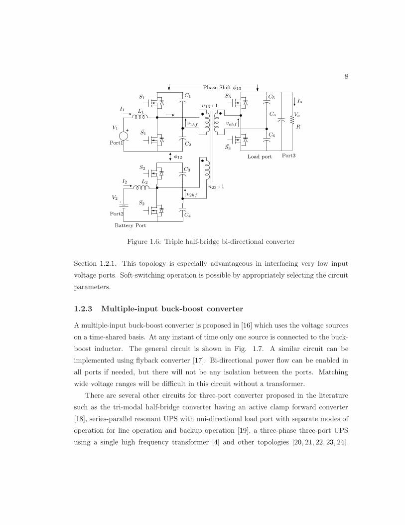
A three-port converter using two boost half-bridges at the input ports is proposed in [15]
to interface batteries and supercapacitors with fuel cell output. The voltages are very
low at the battery and capacitor end and hence a boost half-bridge is used to boost the
voltage and also to create a square wave at the input of the transformer. Such a circuit
is shown in Fig. 1.6. The control of power flow uses the same principle explained in
8
+
−
−
+
n13 : 1
Port3
S3
vohf
Co
Load port
Io
R
Vo
S3
v1hf
v2hf
Phase Shift φ13
Battery Port
S2
S1
S1
V1
I1 L1
S2
V2
I2 L2n23 : 1
φ12
C1
C3
C5
C6
C2
C4Port2
Port1
Figure 1.6: Triple half-bridge bi-directional converter
Section 1.2.1. This topology is especially advantageous in interfacing very low input
voltage ports. Soft-switching operation is possible by appropriately selecting the circuit
parameters.
1.2.3 Multiple-input buck-boost converter
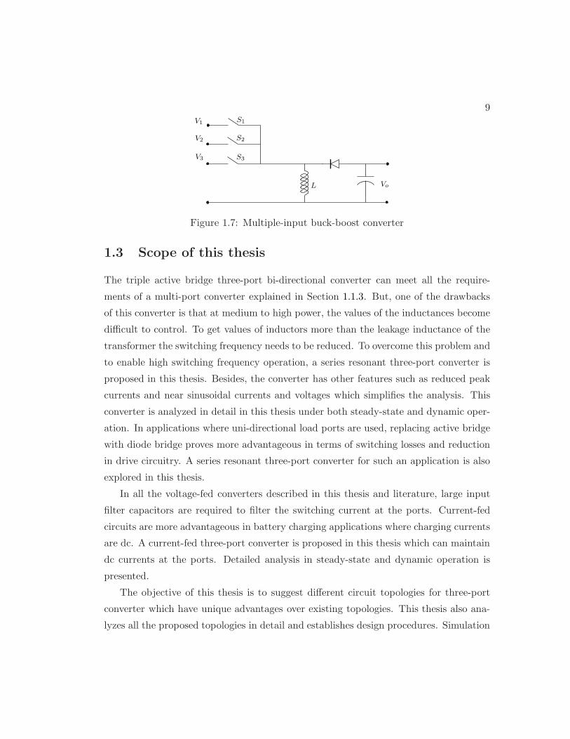
A multiple-input buck-boost converter is proposed in [16] which uses the voltage sources
on a time-shared basis. At any instant of time only one source is connected to the buck-
boost inductor. The general circuit is shown in Fig. 1.7. A similar circuit can be
implemented using flyback converter [17]. Bi-directional power flow can be enabled in
all ports if needed, but there will not be any isolation between the ports. Matching
wide voltage ranges will be difficult in this circuit without a transformer.
There are several other circuits for three-port converter proposed in the literature
such as the tri-modal half-bridge converter having an active clamp forward converter
[18], series-parallel resonant UPS with uni-directional load port with separate modes of
operation for line operation and backup operation [19], a three-phase three-port UPS
using a single high frequency transformer [4] and other topologies [20, 21, 22, 23, 24].
9
L
V2
V3
S1
S2
S3
Vo
V1
Figure 1.7: Multiple-input buck-boost converter
1.3 Scope of this thesis
The triple active bridge three-port bi-directional converter can meet all the require-
ments of a multi-port converter explained in Section 1.1.3. But, one of the drawbacks
of this converter is that at medium to high power, the values of the inductances become
difficult to control. To get values of inductors more than the leakage inductance of the
transformer the switching frequency needs to be reduced. To overcome this problem and
to enable high switching frequency operation, a series resonant three-port converter is
proposed in this thesis. Besides, the converter has other features such as reduced peak
currents and near sinusoidal currents and voltages which simplifies the analysis. This
converter is analyzed in detail in this thesis under both steady-state and dynamic oper-
ation. In applications where uni-directional load ports are used, replacing active bridge
with diode bridge proves more advantageous in terms of switching losses and reduction
in drive circuitry. A series resonant three-port converter for such an application is also
explored in this thesis.
In all the voltage-fed converters described in this thesis and literature, large input
filter capacitors are required to filter the switching current at the ports. Current-fed
circuits are more advantageous in battery charging applications where charging currents
are dc. A current-fed three-port converter is proposed in this thesis which can maintain
dc currents at the ports. Detailed analysis in steady-state and dynamic operation is
presented.
The objective of this thesis is to suggest different circuit topologies for three-port
converter which have unique advantages over existing topologies. This thesis also ana-
lyzes all the proposed topologies in detail and establishes design procedures. Simulation

10
and experimental results are presented to augment the analysis.
1.4 Contributions of this thesis
The contributions of this thesis are:
1. A novel series resonant three-port dc-dc converter with two series resonant tanks,
three-winding transformer and three active bridges phase-shifted from each other
for power flow control.
2. Detailed steady-state analysis of the converter to determine output voltage, port
power, tank currents, tank voltages and soft-switching operation boundary.
3. Dynamic analysis of the converter using generalized averaging theory and con-
troller design to control the output voltage and port powers.
4. Phase-shift control techniques for the series resonant three-port converter with uni-
directional load port configuration and detailed steady-state analysis to determine
the converter variables.
5. Design procedure, simulation and experimental results for both configurations of
series resonant three-port converter
6. A novel current-fed three-port dc-dc converter for achieving dc currents at the
ports
7. Steady-state and dynamic analysis of the current-fed three-port converter
1.5 Organization of this thesis
Chapter 1 introduces the three-port converter and its applications. The existing lit-
erature on three-port converter is explained. In Chapter 2 the series resonant three-
port converter is introduced and steady-state analysis is presented. The three-winding
transformer model and its effect on steady-state performance is also examined. To
understand the dynamic response of the converter, a dynamic model is derived and
closed-loop control design is explained in Chapter 3. The design of the series resonant

11
three-port converter is explained in Chapter 4 and simulation and experimental results
are presented to verify the analysis. For uni-directional output configuration, phase-shift
control techniques are proposed in Chapter 5 and detailed analysis is presented along
with simulation and experimental results. For applications where dc current is desired
at the ports, a current-fed topology is proposed and analyzed in Chapter 6. The design
of such a converter is also presented along with simulation and experimental results.
The last chapter concludes this thesis.
1.6 Conclusion
In this chapter the context of the thesis is established. The multi-port converter is in-
troduced and its applications explained. Existing topologies of the three-port converter
are described. The scope and contributions of this thesis are given.

Chapter 2
Three-port Series Resonant
Converter - Steady-state Analysis
Series resonant dc-dc converters are used in several applications such as high-voltage
and high-density power supplies. These converters have zero switching losses due to
soft-switching and hence reduced size and higher power density when compared to
conventional dc-dc converters. They are mostly uni-directional with only two ports,
source and load. With proliferation of distributed renewable energy sources, there has
been recently lot of interest in integrating the source, energy storage and the load into a
single stage power conversion. Resonant converters are the choice for such applications
due to the aforementioned advantages. In this chapter, a three-port series resonant
dc-dc converter using a single-stage power conversion is proposed and analyzed.
2.1 Principle of operation
2.1.1 Two-port series resonant converter
The two-port series resonant converter which is well known in literature is shown in
Fig 2.1. The transformer turns ratio is taken to be unity. The phase shift θ is between
the square-wave outputs of the active bridges at either end of the resonant tank. The
switching frequency Fs is constant. The resonant tank voltages and currents can be
assumed to be sinusoidal due to the filtering action of the resonant circuit. Hence only
12

13
+
−
+
−
1 : 1L1Cf1
iL1
S3 S3
vohf
Co
S1 S1
v1hf
C1
Phase Shift θ
Io
RPort1
V1
i1lf
Vo
iolf
S3S3S1S1
iohf
I1
Figure 2.1: Two-port series resonant converter with two active bridges
the fundamental of the applied square wave can be used in the calculation of tank
current. The output voltage Vo of the converter is given in (2.1).
Vo =V1
Q1(F1 − 1F1
)sin θ (2.1)
where Q1 =Z18π2 R
; Z1 =
√
L1
C1; F1 =
ωs
ω1; ωs = 2πFs ; ω1 =
1√L1C1
;
Vo =V1
√
1 + Q21
(
F1 − 1F1
)2Load-side diode bridge (2.2)
There are several methods suggested in literature in varying the output voltage,
1. Phase shift angle θ [25].
2. Switching frequency Fs which changes the impedance provided by the resonant
tank [7].
3. Voltage magnitudes by pulse width modulation of the active bridges at constant
switching frequency Fs [26].
For very high output voltage applications, the active bridge at load side is replaced by
a diode bridge. This results in the conventional series resonant converter whose output
voltage is given by (2.2). It is observed that for the same switching frequency and
quality ratio, the output voltage is higher with active bridge at the load side. In this
Chapter the proposed converter uses phase shift angle between active bridges to control
output voltage under constant switching frequency and constant voltage magnitudes.
14
−
+
+
−
+
−
+
−
+ −
+ −
+
−
L1Cf1
Cf2
iL1
iL2
Port3
n13 : 1
S3 S3
vohf
Co
S1 S1
S2 S2
L2C2
C1
Phase Shift φ12 Load port
Phase Shift φ13
RPort1
Battery Port
V1
V2
i1lf
i2lf
iolf
S3S3
S2S2
S1S1
n23 : 1
iohf
I1
I2
Series Resonant
Series Resonant
Tank2
Tank1
vC1
vC1
vo
Port2
Figure 2.2: Proposed three-port series resonant converter circuit
2.1.2 Three-port series resonant converter
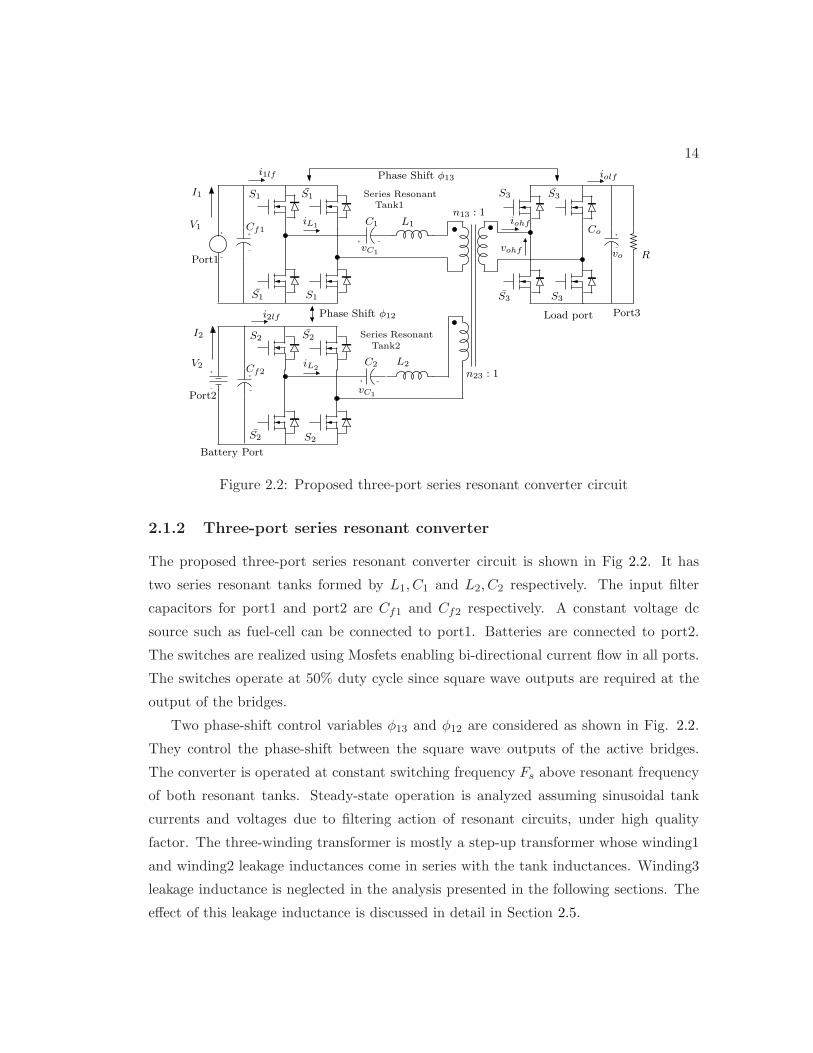
The proposed three-port series resonant converter circuit is shown in Fig 2.2. It has
two series resonant tanks formed by L1, C1 and L2, C2 respectively. The input filter
capacitors for port1 and port2 are Cf1 and Cf2 respectively. A constant voltage dc
source such as fuel-cell can be connected to port1. Batteries are connected to port2.
The switches are realized using Mosfets enabling bi-directional current flow in all ports.
The switches operate at 50% duty cycle since square wave outputs are required at the
output of the bridges.
Two phase-shift control variables φ13 and φ12 are considered as shown in Fig. 2.2.
They control the phase-shift between the square wave outputs of the active bridges.
The converter is operated at constant switching frequency Fs above resonant frequency
of both resonant tanks. Steady-state operation is analyzed assuming sinusoidal tank
currents and voltages due to filtering action of resonant circuits, under high quality
factor. The three-winding transformer is mostly a step-up transformer whose winding1
and winding2 leakage inductances come in series with the tank inductances. Winding3
leakage inductance is neglected in the analysis presented in the following sections. The
effect of this leakage inductance is discussed in detail in Section 2.5.

15
IL2
(a) (b)(c)
V1
V2
Vo
v1hf
v2hf
vohf
φ13
φ12
iL2
iL1
iohf
θ1
θ2
θ3
φ12
φ13
i1lf
i2lf
iolf
IL1
I3
Ts
2
Figure 2.3: (a) PWM waveforms with definitions of phase-shift variables φ13 and φ12
(b) Tank currents and transformer winding3 current (c) Port currents before filter
2.1.3 Analysis of port voltages and currents
The square wave outputs and the corresponding phase shifts are shown in Fig. 2.3.
The phase-shifts φ13 and φ12 are considered positive if vohf lags v1hf and v2hf lags v1hf
respectively. The waveforms of the tank currents and port currents before the filter
are shown in Fig. 2.3b and 2.3c respectively. Phasor analysis is used to calculate the
following quantities: IL1∠θ1, IL2∠θ2, IL3∠θ3, I1, I2, Io and Vo.
The average value of the unfiltered output current iolf in Fig. 2.3c is given by
(2.3). Phasor analysis is used to calculate I3 (2.4), which is the peak of the transformer
winding3 current. After substitution, the resultant expression for output current is
(2.5).
Io =2
πI3 cos (φ13 − θ3) (2.3)
where I3∠θ3 = n13IL1∠θ1 + n23IL2∠θ2 (2.4)
IL1∠θ1 =4πV1∠0 − 4
πn13Vo∠φ13
jωsL1 + 1jωsC1
IL2∠θ2 =4πV2∠φ12 − 4
πn23Vo∠φ13
jωsL2 + 1jωsC2
Simplifying Io =8
π2
n13V1
Z1(F1 − 1F1
)sin φ13 +
8
π2
n23V2
Z2(F2 − 1F2
)sin (φ13 − φ12) (2.5)
where Zi =
√
Li
Ci; Fi =
ωs
ωi; ωs = 2πfs ; ωi =
1√LiCi
; i = 1, 2 (2.6)

16
If the load resistance is R, the output voltage is Vo = IoR as given by,
Vo =V1n13
Q1(F1 − 1F1
)sinφ13 +
V2n23
Q2(F2 − 1F2
)sin (φ13 − φ12) (2.7)
where Qi =Zi
8π2 Rn2
i3
for i = 1, 2 (2.8)
The average value of port1 current i1lf from Fig. 2.3c can be expressed as in (2.9).
Substituting the peak resonant tank1 current IL1 from phasor analysis, the port1 dc
current is then given by (2.10). Similar derivation is done for port2 and the results are
given in (2.11) and (2.12).
I1 =2
πIL1 cos (θ1) (2.9)
=8
π2
n13Vo
Z1(F1 − 1F1
)sin φ13 (2.10)
I2 =2
πIL2 cos (θ2 − φ12) (2.11)
=8
π2
n23Vo
Z2(F2 − 1F2
)sin (φ13 − φ12) (2.12)
The analysis results are normalized to explain the characteristics of the converter, to
compare with existing circuit topologies and to establish a design procedure. Consider
a voltage base Vb and a power base Pb. For design calculations, the base voltage is used
as the required output voltage and the base power as the maximum output power. The
variable m1 (2.13), termed as voltage conversion ratio, is defined as the normalized value
of port1 input voltage referred to port1 side using turns ratio n13. Similar definition
applies for m2 (2.13). The per unit output voltage is then given by (2.14).
m1 =V1
n13Vb
; m2 =V2
n23Vb
; (2.13)
Vo,pu =Vo
Vb
=m1
Q1(F1 − 1F1
)sin φ13 +
m2
Q2(F2 − 1F2
)sin (φ13 − φ12) (2.14)
A plot of per unit output voltage using (2.14) is shown in Fig. 2.4a and 2.4b. In
the plot, the values of m1 and m2 are chosen as 1.0. The reason for this is to maximize
17
−90 −45 0 45 900
0.5
1
1.5
2
2.5
3
Phase-shift angle φ12 degrees
Outp
ut
voltag
eV
o,p
u
φ13 = 30
φ13 = 60
φ13 = 90
(a)
−90 −45 0 45 900
2
4
6
Phase-shift angle φ12 degrees
Outp
ut
voltag
eV
o,p
u
Q=2Q=3Q=4
(b)
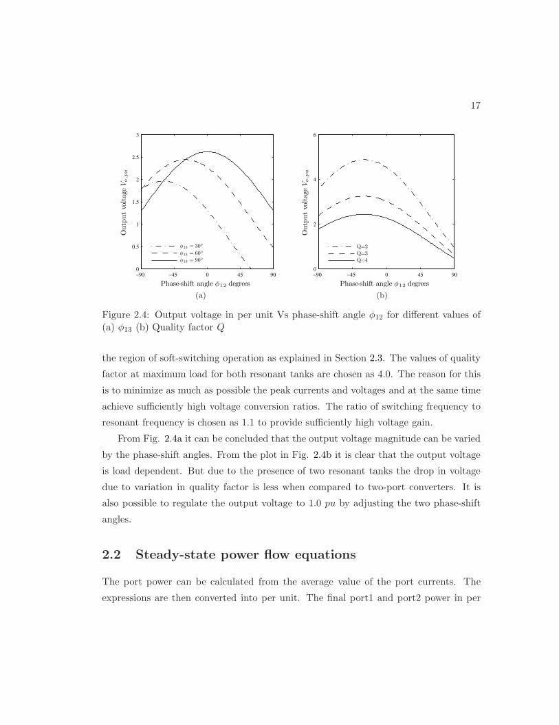
Figure 2.4: Output voltage in per unit Vs phase-shift angle φ12 for different values of(a) φ13 (b) Quality factor Q
the region of soft-switching operation as explained in Section 2.3. The values of quality
factor at maximum load for both resonant tanks are chosen as 4.0. The reason for this
is to minimize as much as possible the peak currents and voltages and at the same time
achieve sufficiently high voltage conversion ratios. The ratio of switching frequency to
resonant frequency is chosen as 1.1 to provide sufficiently high voltage gain.
From Fig. 2.4a it can be concluded that the output voltage magnitude can be varied
by the phase-shift angles. From the plot in Fig. 2.4b it is clear that the output voltage
is load dependent. But due to the presence of two resonant tanks the drop in voltage
due to variation in quality factor is less when compared to two-port converters. It is
also possible to regulate the output voltage to 1.0 pu by adjusting the two phase-shift
angles.
2.2 Steady-state power flow equations
The port power can be calculated from the average value of the port currents. The
expressions are then converted into per unit. The final port1 and port2 power in per

18
unit after simplifications are given by (2.15) and (2.16) respectively.
P1,pu =P1
Pb
=m1Io,pu
Q1
(
F1 − 1F1
) sin φ13 (2.15)
P2,pu =P2
Pb
=m2Io,pu
Q2
(
F2 − 1F2
) sin (φ13 − φ12) (2.16)
Po,pu = P1,pu + P2,pu (2.17)
where Rb =V 2
b
Pb
; Ib =Vb
Rb
; Rpu =R
Rb
; Io,pu =Io
Ib
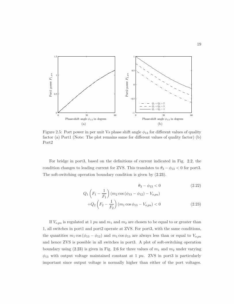
Plots of port1 and port2 power in per unit as a function of phase-shift φ13 are shown
in Fig. 2.5a and 2.5b for three different quality factors. Since there are two phase-shift
variables, phase-shift φ13 is varied and the phase-shift φ12 is chosen such that the output
voltage in per unit Vo,pu is kept constant at 1 pu. The output power Po,pu at maximum
load Q = 4.0 is 1.0 pu. It is observed from Fig. 2.5a that the port1 power does not vary
with load as long as output voltage is maintained constant. The phase-shift φ13 is kept
positive for uni-directional power flow in port1. Port2 power P2,pu can go negative as
seen from the plot and hence used as the battery port. In the plots, the values of m1
and m2 are chosen as 1.0 and F1 and F2 as 1.1.
2.3 Soft-switching operation boundary
The conditions for soft-switching operation in the active bridges can be derived from
Fig. 2.3. If port1 and port2 tank currents lag their applied square wave voltages, then
all switches in port1 and port2 bridges operate at Zero Voltage Switching (ZVS). This
translates to θ1 > 0 for port1 and θ2−φ12 > 0 for port2. Note that angles are considered
positive if lagging, in the analysis. Using phasor analysis, the soft-switching operation
boundary conditions are given by (2.19) and (2.21) for port1 and port2 respectively.
θ1 > 0 For Port1 (2.18)
Vo,pu cos φ13 − m1 < 0 For Port1 (2.19)
θ2 − φ12 > 0 For Port2 (2.20)
Vo,pu cos (φ13 − φ12) − m2 < 0 For Port2 (2.21)
19
0 30 600
0.5
1
1.5
Phase-shift angle φ13 in degrees
Por
t1pow
erP
1,p
u
(a)
0 30 60−1
−0.5
0
0.5
1
Phase-shift angle φ13 in degrees
Por
t2pow
erP
2,p
u
Q1 = Q2 = 2Q1 = Q2 = 3Q1 = Q2 = 4
(b)
Figure 2.5: Port power in per unit Vs phase shift angle φ13 for different values of qualityfactor (a) Port1 (Note: The plot remains same for different values of quality factor) (b)Port2
For bridge in port3, based on the definitions of current indicated in Fig. 2.2, the
condition changes to leading current for ZVS. This translates to θ3 − φ13 < 0 for port3.
The soft-switching operation boundary condition is given by (2.23).
θ3 − φ13 < 0 (2.22)
Q1
(
F1 −1
F1
)
(m2 cos (φ13 − φ12) − Vo,pu)
+Q2
(
F2 −1
F2
)
(m1 cos φ13 − Vo,pu) < 0 (2.23)
If Vo,pu is regulated at 1 pu and m1 and m2 are chosen to be equal to or greater than
1, all switches in port1 and port2 operate at ZVS. For port3, with the same conditions,
the quantities m1 cos (φ13 − φ12) and m1 cos φ13 are always less than or equal to Vo,pu
and hence ZVS is possible in all switches in port3. A plot of soft-switching operation
boundary using (2.23) is given in Fig. 2.6 for three values of m1 and m2 under varying
φ13 with output voltage maintained constant at 1 pu. ZVS in port3 is particularly
important since output voltage is normally higher than either of the port voltages.

20
30 60−2
−1
0
1
2
Phase-shift angle φ13 in degrees
Port
3 s
oft
−sw
itch
ing o
per
atio
n b
oundar
y
m1 = m2 = 0.75m1 = m2 = 1.0m1 = m2 = 1.25
Figure 2.6: Port3 soft-switching operation boundary for various values of m1 and m2
Hence in design m1 and m2 are chosen to be 1.
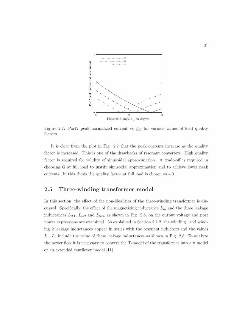
2.4 Peak currents in tank circuit
The peak tank currents IL1 and IL2 are normalized with respect to corresponding tank
impedance. The final expressions are given by (2.24) and (2.25). A plot of port2 peak
current as a function of φ13 for various values of load quality factors is shown in Fig.
2.7. In this plot φ12 is chosen in such a way to maintain output voltage constant at
1 pu. Also, the values of m1 and m2 are chosen as 1.0. From Fig. 2.7 and Fig. 2.5b,
it can be observed that port2 peak tank current is maximum when it is supplying the
full load and is minimum when it is not supplying any power. In Chapter 4, a specific
design is explained and peak currents are calculated for all operating conditions.
IL1(norm) =4
π
√
1 +
(
Vo,pu
m1
)2
− 2Vo,pu
m1cos φ13 (2.24)
IL2(norm) =4
π
√
1 +
(
Vo,pu
m2
)2
− 2Vo,pu
m2cos (φ13 − φ12) (2.25)
where ILi(norm) =ILi
Zi
(
Fi − 1Fi
) ; i = 1, 2 (2.26)
21
0 30 600
1
2
Phase-shift angle φ13 in degrees
Port
2 p
eak n
orm
aliz
ed t
ank c
urr
ent
Q1 = Q2 = 2Q1 = Q2 = 3Q1 = Q2 = 4
Figure 2.7: Port2 peak normalized current vs φ13 for various values of load qualityfactors
It is clear from the plot in Fig. 2.7 that the peak currents increase as the quality
factor is increased. This is one of the drawbacks of resonant converters. High quality
factor is required for validity of sinusoidal approximation. A trade-off is required in
choosing Q at full load to justify sinusoidal approximation and to achieve lower peak
currents. In this thesis the quality factor at full load is chosen as 4.0.
2.5 Three-winding transformer model
In this section, the effect of the non-idealities of the three-winding transformer is dis-
cussed. Specifically, the effect of the magnetizing inductance Lm and the three leakage
inductances Llk1, Llk2 and Llk3, as shown in Fig. 2.8, on the output voltage and port
power expressions are examined. As explained in Section 2.1.2, the winding1 and wind-
ing 2 leakage inductances appear in series with the resonant inductors and the values
L1, L2 include the value of these leakage inductances as shown in Fig. 2.8. To analyze
the power flow it is necessary to convert the T-model of the transformer into a π model
or an extended cantilever model [11].
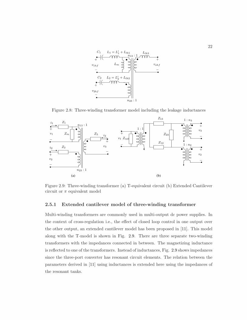
22
n13 : 1C1
C2
Llk3
v1hf
v2hf
vohf
n23 : 1
+
−
+
−
+
−
L1 = L′
1 + Llk1
L2 = L′
2 + Llk2
Lm
Figure 2.8: Three-winding transformer model including the leakage inductances
(a) (b)
v2
n23 : 1
n13 : 1
v3
+
−
Z2
Z1
Zm Z3 i3v1
+
−
i1
i2
+
v2
−
1 : 1
Z23
Z13
Z12
1 : n3
1 : n2
+
−
v1 Zm0
+
−
v3
+
−
Figure 2.9: Three-winding transformer (a) T-equivalent circuit (b) Extended Cantilevercircuit or π equivalent model
2.5.1 Extended cantilever model of three-winding transformer
Multi-winding transformers are commonly used in multi-output dc power supplies. In
the context of cross-regulation i.e., the effect of closed loop control in one output over
the other output, an extended cantilever model has been proposed in [11]. This model
along with the T-model is shown in Fig. 2.9. There are three separate two-winding
transformers with the impedances connected in between. The magnetizing inductance
is reflected to one of the transformers. Instead of inductances, Fig. 2.9 shows impedances
since the three-port converter has resonant circuit elements. The relation between the
parameters derived in [11] using inductances is extended here using the impedances of
the resonant tanks.

23
Using the T-model in Fig. 2.9, we can write,
v1
v2
v3
=
Z1 + Zm Zmn23n13
Zm1
n13
Zmn23n13
Z2 + Zmn2
23
n213
Zmn23
n213
Zm1
n13Zm
n23
n213
Z3 + Zm1
n213
i1
i2
i3
(2.27)
V = ZI = (zjk) (2.28)
Y = Z−1 = (bjk) j 6= k (2.29)
Then the elements of the equivalent model in Fig. 2.9 can be represented as,
Zm0 = Zm + Z1 (2.30)
n2 =z12
z11=
Zm
Z1 + Zm
n23
n13(2.31)
n1 =z13
z11=
Zm
Z1 + Zm
1
n13(2.32)
Zjk = − 1
njnkbjk
j 6= k (2.33)
Using (2.33), the values of Z12, Z13 and Z23 in the π equivalent model can be
determined. The parameters in the extended cantilever model can be directly measured,
but since the three-port converter has external inductance and capacitor connected in
series, the parameters of the T-model of the transformer are individually determined
first and then the circuit in Fig. 2.8 is transformed to the extended cantilever model.
2.5.2 Power flow equations using the equivalent model
The power flow between port1 and port3 assuming sinusoidal voltages and currents is
given by,
P13 =16
π2
V1V21n2
Z13sin φ13 (2.34)
v1 =4
πV1 sin ωst (2.35)
v2 =4
πV2 sin (ωst − φ13) (2.36)
Z13 =
(
Z1 + Zm
Zm
)
(
Z1Zm(Z2 + n223Z3) + n2
13Z2Z3(Z1 + Zm)
Z2Zm
)
(2.37)

24
Simplifying this equation and representing in per unit, the power flow between port1
and port3 P13,pu (2.38) is obtained.
P13,pu =m1Io,pu sin φ13
Q1
(
F1 − 1F1
)
+ Qlk3
1 + Q1
Qm
(
F1 − 1F1
)
+ Q1
Q2
(
F1−1
F1
)
(
F2−1
F2
)
(2.38)
Qlk3 =ωsLlk3
8π2 R
; Qm =ωsLm
8π2 n2
13R(2.39)
Similarly the two other power flow equations are derived and given in (2.40) and
(2.41) respectively. Using the power flow between ports, the total power from each of
the ports can be determined using (2.42-2.44).
P12,pu =m1m2/Rpu sinφ12
Q1
(
F1 − 1F1
)
+ Q2
(
F2 − 1F2
) (
1 + Q1
Qm
(
F1 − 1F1
)
+ Q1
Qlk3
(
F1 − 1F1
))(2.40)
P23,pu =m2Io,pu sin (φ13 − φ12)
Q2
(
F2 − 1F2
)
+ Qlk3
1 + Q2
Qm
(
F2 − 1F2
)
+ Q2
Q1
(
F2−1
F2
)
(
F1−1
F1
)
(2.41)
P1,pu = P13,pu + P12,pu (2.42)
P2,pu = P23,pu − P12,pu (2.43)
Po,pu = P1,pu + P2,pu (2.44)
To summarize, following are the steps involved in determining the extended can-
tilever model:
1. Measure the parameters in the T-model of the transformer i.e., Llk1, Llk2, Llk3
and Lm.
2. Construct the T-model along with the resonant circuit elements as in Fig. 2.8.
3. Transform the T-model to the extended cantilever model and determine the equiv-
alent circuit parameters Zm0, Z12, Z23, Z13, n2 and n3.

25
4. Calculate the power flow between ports and hence the net power flow from each
of the ports
The magnetizing inductance Lm is very large when compared to the impedance
offered by the resonant tank circuit and hence Qm ≫ Q1
(
F1 − 1F1
)
. Since the resonant
tank circuit operates at high quality factor Q ≥ 4, it can be assumed that Qlk3 ≪Qi
(
Fi − 1Fi
)
with Fi = 1.1. With the above two simplifying assumptions along with
the high impedance between port1 and port2 contributed by Q1 and Q2 in (2.40), the
power flow between port1 and port2, P12,pu, is negligible. Also the power flow between
port1 and port3, P13,pu, reduces to P1,pu in (2.15). In the following sections, these
assumptions are applied. In Section 4.2.3, a plot of the phase shifts with and without
the leakage inductance Llk3 is given.
2.6 Conclusion
In this chapter the three-port series resonant converter is proposed. Steady state analysis
is presented to determine the power flow equations in the three-port converter. It can
be concluded from the analysis that the power flow between ports in any direction can
be controlled by the phase-shift angles. Further, soft-switching operation is possible in
the full operating range of the converter provided the design constraints are met. The
effect of non-idealities in the three-winding transformer on the power flow between ports
are discussed using an equivalent model.
Chapter 3
Three-port Series Resonant
Converter - Dynamic Analysis
Dynamic analysis of the proposed three-port series resonant converter is presented in
this Chapter. The analysis aids in designing controller for regulating power flow in
the converter. The analysis approach uses averaging and time-scaling with sinusoidal
approximation. Different approaches for feedback controller design are also discussed in
this Chapter.
3.1 Dynamic equations for the converter
The triple active bridge series resonant converter is shown in Fig. 3.1. Dynamic equa-
tions are given for the resonant tank currents, tank voltages and the output voltage
(3.1-3.5). The variable ωs is defined as ωs = 2πFs where Fs is the switching frequency.
The voltage polarity and current direction are indicated in the Fig. 3.1.
L1iL1 = V1 sgn(sin (ωst)) − vC1 − n13vo sgn(sin (ωst − φ13)) (3.1)
C1vC1 = iL1 (3.2)
L2iL2 = V2 sgn(sin (ωst − φ12)) − vC2 − n23vo sgn(sin (ωst − φ13)) (3.3)
C2vC2 = iL2 (3.4)
Covo = (n13iL1 + n23iL2) sgn(sin (ωst − φ13)) −vo
R(3.5)
26
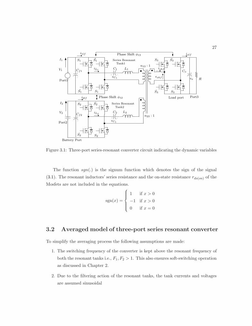
27
−
+
+
−
+
−
+
−
+ −
+ −
+
−
L1Cf1
Cf2
iL1
iL2
Port3
n13 : 1
S3 S3
vohf
Co
S1 S1
S2 S2
L2C2
C1
Phase Shift φ12 Load port
Phase Shift φ13
RPort1
Battery Port
V1
V2
i1lf
i2lf
iolf
S3S3
S2S2
S1S1
n23 : 1
iohf
I1
I2
Series Resonant
Series Resonant
Tank2
Tank1
vC1
vC1
vo
Port2
Figure 3.1: Three-port series-resonant converter circuit indicating the dynamic variables
The function sgn(.) is the signum function which denotes the sign of the signal
(3.1). The resonant inductors’ series resistance and the on-state resistance rds(on) of the
Mosfets are not included in the equations.
sgn(x) =
1 if x > 0
−1 if x > 0
0 if x = 0
3.2 Averaged model of three-port series resonant converter
To simplify the averaging process the following assumptions are made:
1. The switching frequency of the converter is kept above the resonant frequency of
both the resonant tanks i.e., F1, F2 > 1. This also ensures soft-switching operation
as discussed in Chapter 2.
2. Due to the filtering action of the resonant tanks, the tank currents and voltages
are assumed sinusoidal

28
With the above assumptions, an averaged model for the converter can be derived. The
following section explains the method adopted for averaging this circuit.
3.2.1 Generalized averaging method
The generalized averaging method was proposed in [27] to analyze all types of switching
converters. It is briefly explained here from [27] and applied for the proposed converter.
A waveform x(·) can be approximated on the interval (t − T, t] with a Fourier series
representation of the form
x(t − T + s) =∑
k
< x >k (t)ejkωs(t−T+s) (3.6)
where the sum is over all integers k, ωs = 2π/T, s ∈ (0, T ] and < x >k (t) are complex
Fourier coefficients which can also be referred to as phasors. These Fourier coefficients
are functions of time since the interval under consideration slides as a function of time.
The kth coefficient is determined by
< x >k (t) =1
T
∫ T
ox(t − T + s)e−jkωs(t−T+s) (3.7)
This type of averaging method is used in power electronic circuits where the model has
some periodic time-dependence. In this converter it is the function sgn(sin ωst) having
a period T = 2π/ωs = 1/Fs where Fs is the switching frequency. Some applications of
this method are given in [28,29,30,31,32,33]
3.2.2 Application to three-port converter
Following assumption 2, the states can be approximated with the fundamental frequency
terms in the Fourier series (3.6). This can be obtained by application of the operator
< · >1 and < · >0 to the model (3.1-3.5). The paper [27] also gives some properties of
the Fourier coefficients (3.7) which will be used in further derivations.
⟨
iL1
⟩
1= −jωs 〈iL1〉1 +
1
L1V1 〈sgn(sin (ωst))〉1 −
1
L1〈vC1〉1
− n13
L1〈vo sgn(sin (ωst − φ13))〉1 (3.8)
〈vC1〉1 = −jωs 〈vC1〉1 +1
C1〈iL1〉1 (3.9)

29⟨
iL2
⟩
1= −jωs 〈iL2〉1 +
1
L2V2 〈sgn(sin (ωst − φ12))〉1 −
1
L2〈vC2〉1
− n23
L2〈vo sgn(sin (ωst − φ13))〉1 (3.10)
〈vC2〉1 = −jωs 〈vC2〉1 +1
C2〈iL2〉1 (3.11)
〈vo〉0 =1
Co〈(n13iL1 + n23iL2) sgn(sin (ωst − φ13))〉0 −
〈vo〉0RCo
(3.12)
The evaluation of Fourier series coefficients for the important terms in (3.8-3.12) is
given below.
〈sgn sin (ωst − φ13)〉1 = −j2
πe−jφ13 (3.13)
〈vo sgn(sin (ωst − φ13))〉1 = 〈vo〉0 〈sgn(sin (ωst − φ13))〉1 (3.14)
〈(iL1 + iL2)sgn(sin (ωst − φ13))〉0 = 〈(iL1 + iL2)〉−1 〈sgn(sin (ωst − φ13))〉1+ 〈(iL1 + iL2)〉1 〈sgn(sin (ωst − φ13))〉−1(3.15)
The generalized averaging method is applied to the converter with the assumption
that only the first harmonics of the tank currents and voltages are retained. These are
denoted by the phasors as in IL1 = IL1∠θ1. In these phasors, both the magnitude and
phase vary with time. The system can then be represented using the tank current and
voltage phasors as in (3.16)-(3.20) usually referred to in literature as dynamic phasor
model. The equations (3.8-3.12) can be rewritten substituting the terms evaluated in
(3.13-3.15).
L1IL1 = −jωsIL1 − j2
πV1 − VC1 + n13Voj
2
πe−jφ13 (3.16)
C1VC1 = −jωsVC1 − IL1 (3.17)
L2IL2 = −jωsIL2 − j2
πV2e
−jφ12 − VC2 + n23Voj2
πe−jφ13 (3.18)
C2VC2 = −jωsVC2 − IL2 (3.19)
Covo = −j2
πn13IL1e
−jφ13 + j2
πn13IL1e
jφ13
− j2
πn23IL2e
−jφ13 + j2
πn23IL2e
jφ13 − vo
R(3.20)

30
It is known that the Fourier series coefficient 〈·〉1 is a complex value. Hence the state
equations (3.16-3.20) can be expanded into 9 state equations considering the dynamics
of both the real and imaginary terms of the coefficients. The states are redefined as
follows,
〈iL1〉1 = x1 + jx2 (3.21)
〈vC1〉1 = x3 + jx4 (3.22)
〈iL2〉1 = x5 + jx6 (3.23)
〈vC2〉1 = x7 + jx8 (3.24)
〈vo〉0 = x9 (3.25)
After simplification, the final state space equations with 9 states are given by (3.26-
3.34),
x1 = ωsx2 −1
L1x3 +
1
L1
2
πn13x9 sin φ13 (3.26)
x2 = −ωsx1 −1
L1x4 +
1
L1
2
πn13x9 cos φ13 −
2
π
V1
L1(3.27)
x3 = ωsx4 +1
C1x1 (3.28)
x4 = −ωsx3 +1
C1x2 (3.29)
x5 = ωsx6 −1
L2x7 +
1
L2
2
πn23x9 sin φ13 −
2
π
V2
L2sin φ12 (3.30)
x6 = −ωsx5 −1
L2x8 +
1
L2
2
πn23x9 cos φ13 −
2
π
V2
L2cos φ12 (3.31)
x7 = ωsx8 +1
C2x5 (3.32)
x8 = −ωsx7 +1
C2x6 (3.33)
x9 = − 1
Co
4
πn13x1 sin φ13 −
1
Co
4
πn23x5 sinφ13
− 1
Co
4
πn13x2 cos φ13 −
1
Co
4
πn23x6 cos φ13 −
x9
RCo(3.34)

31
3.3 Normalization of the state equations
The system of equations (3.26-3.34) can be normalized to obtain dimensionless expres-
sions. The normalized variables for resonant tank1 are defined in (3.35-3.36). Similar
definitions apply for resonant tank2. The normalized output voltage state is given in
(3.39). The time t is also normalized by using tn = t/(RCo).
x1n =x1
V1/√
L1C1
x5n =x5
V2/√
L2C2
(3.35)
x2n =x2
V1/√
L1C1
x6n =x6
V2/√
L2C2
(3.36)
x3n =x3
V1x7n =
x7
V2(3.37)
x4n =x4
V1x8n =
x8
V2(3.38)
x9n =x9V1
n13m1
=x9V2
n23m2
(3.39)
The normalized state equations (3.40-3.48) are obtained by substituting the defin-
tions for the normalized state variables including the normalized time tn.
ǫx1n = F1x2n − x3n +2
π
1
m1x9n sin φ13 (3.40)
ǫx2n = −F1x1n − x4n +2
π
1
m1x9n cos φ13 −
2
π(3.41)
ǫx3n = F1x4n + x1n (3.42)
ǫx4n = −F1x3n + x2n (3.43)
ǫx5n = F2x6n − x7n +2
π
1
m2x9n sin φ13 −
2
πsin φ12 (3.44)
ǫx6n = −F2x5n − x8n +2
π
1
m2x9n cos φ13 −
2
πcos φ12 (3.45)
ǫx7n = F2x8n + x5n (3.46)
ǫx8n = −F2x7n + x6n (3.47)
x9n = − 4
π
m1
Q1x1n sinφ13 −
4
π
m1
Q1x2n cos φ13
− 4
π
m2
Q2x5n sin φ13 −
4
π
m2
Q2x6n cos φ13 − x9n (3.48)

32
3.3.1 Steady-state results using averaged model
Steady state solutions can be obtained by equating the dynamics of (3.40-3.48) to zero.
Steady state solution depends on the constant input voltages V1, V2 and the load resis-
tance R. The phase shifts φ12 and φ13 are the inputs used for control. The steady-state
value X9n is given in (3.49) which is same as the solution obtained in (2.14). The
solutions of the remaining states as a function of X9n are given in (3.50-3.57).
X9n =m1
Q1
(
F1 − 1F1
) sin φ13 +m2
Q2
(
F2 − 1F2
) sin (φ13 − φ12) (3.49)
X1n =2
π
1(
F1 − 1F1
)
[
−1 +1
m1X9n cos φ13
]
(3.50)
X2n =2
π
1(
F1 − 1F1
)
[
− 1
m1X9n sin φ13
]
(3.51)
X3n =1
F1X2n (3.52)
X4n = − 1
F1X1n (3.53)
X5n =2
π
1(
F2 − 1F2
)
[
− cos φ12 +1
m2X9n cos φ13
]
(3.54)
X6n =2
π
1(
F2 − 1F2
)
[
sin φ12 −1
m2X9n sin φ13
]
(3.55)
X7n =1
F2X6n (3.56)
X8n = − 1
F2X5n (3.57)
3.4 Time-Scaling for the dynamic system
The original system (3.1-3.5) has been converted to the autonomous system (3.40-3.48)
using averaging, sinusoidal approximation and normalization. These equations can be
now represented in a standard singular perturbation model (3.58-3.59) with a small

33
parameter ǫ defined as√
LiCi/RCo.
x = f(x, z, ǫ) (3.58)
ǫz = g(x, z, ǫ) (3.59)
where z = [x1 x2 x3 x4 x5 x6 x7 x8 x9]T ; x = x9 (3.60)
ǫ =
√LiCi
RCo
i = 1, 2 (3.61)
Considering that in the design, the resonant frequency of both the resonant tanks
are almost the same, the parameter ǫ remains the same for both resonant tanks. The
capacitor Co is large to filter the switching ripple current at the output port. The
time constant RCo is very large when compared to the resonant tank period. In the
hardware prototype it is 105 times larger than the resonant tank time constant. Hence
the perturbation parameter ǫ is very small.
Setting ǫ = 0 in (3.59) gives the solution for states as in (3.50-3.57) considering the
inputs to the system, the phase shifts φ12 and φ13, are kept constant. This solution
as a function of the state x is referred to as the quasi-steady state z. These equations
are given in (3.50-3.57). The boundary-layer system [34] is found to be globally expo-
nentially stable if the series resistances of the inductor, Mosfet on-state resistance are
included in the state equations. The reduced model can be written as in (3.62) where
u∗ is the pseudo-control input. This has an unique solution as given in (3.64).
x = u∗ − x (3.62)
where u∗ =m1
Q1(F1 − 1F1
)sin (φ13) +
m2
Q2(F2 − 1F2
)sin (φ13 − φ12) (3.63)
x(tn) = u∗(
1 − e−tn)
x(0) = 0 (3.64)
3.5 Controller design
Since the system can be represented in two timescales, the overall feedback system can
be represented as in Fig. 3.2 using a static non-linear block whose input is the pseudo-
control input Io(ref). The phase-shifts φ12 and φ13 are calculated from (3.65) and (3.66)
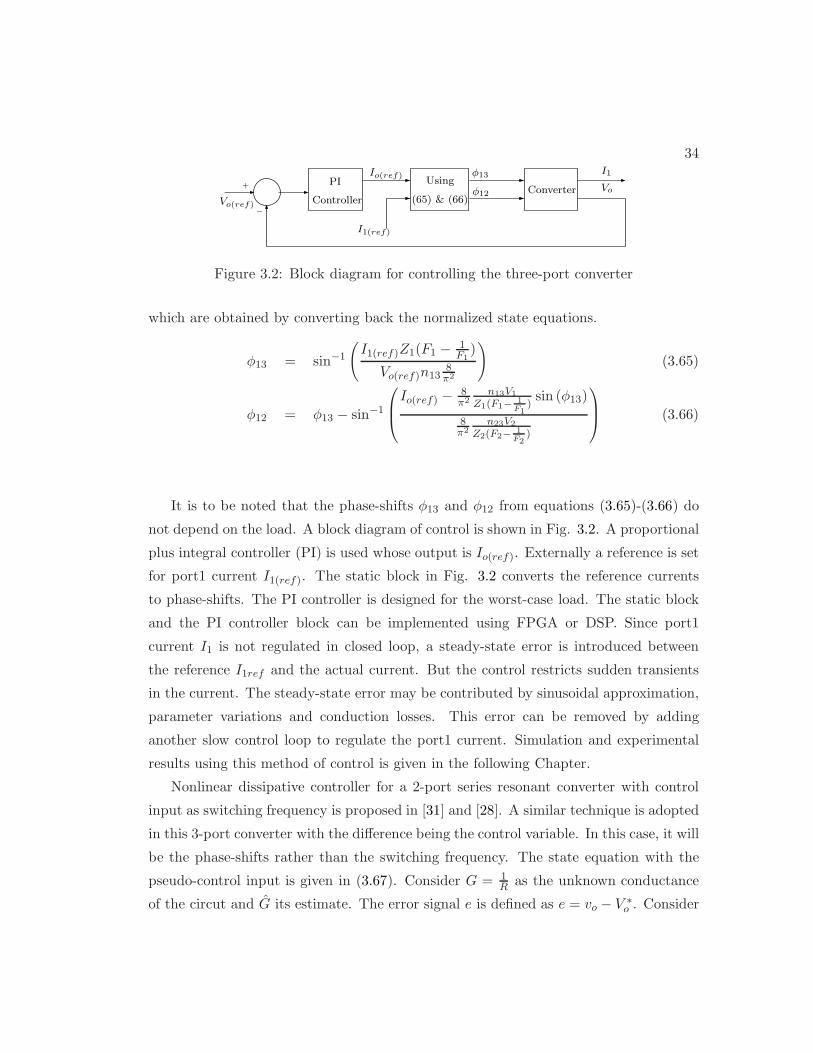
34
I1(ref)
−
+
Io(ref)Using
φ12
I1
Vo
φ13
Vo(ref)(65) & (66)
PI
ControllerConverter
Figure 3.2: Block diagram for controlling the three-port converter
which are obtained by converting back the normalized state equations.
φ13 = sin−1
(
I1(ref)Z1(F1 − 1F1
)
Vo(ref)n138π2
)
(3.65)
φ12 = φ13 − sin−1
Io(ref) − 8π2
n13V1
Z1(F1−1
F1)sin (φ13)
8π2
n23V2
Z2(F2−1
F2)
(3.66)
It is to be noted that the phase-shifts φ13 and φ12 from equations (3.65)-(3.66) do
not depend on the load. A block diagram of control is shown in Fig. 3.2. A proportional
plus integral controller (PI) is used whose output is Io(ref). Externally a reference is set
for port1 current I1(ref). The static block in Fig. 3.2 converts the reference currents
to phase-shifts. The PI controller is designed for the worst-case load. The static block
and the PI controller block can be implemented using FPGA or DSP. Since port1
current I1 is not regulated in closed loop, a steady-state error is introduced between
the reference I1ref and the actual current. But the control restricts sudden transients
in the current. The steady-state error may be contributed by sinusoidal approximation,
parameter variations and conduction losses. This error can be removed by adding
another slow control loop to regulate the port1 current. Simulation and experimental
results using this method of control is given in the following Chapter.
Nonlinear dissipative controller for a 2-port series resonant converter with control
input as switching frequency is proposed in [31] and [28]. A similar technique is adopted
in this 3-port converter with the difference being the control variable. In this case, it will
be the phase-shifts rather than the switching frequency. The state equation with the
pseudo-control input is given in (3.67). Consider G = 1R
as the unknown conductance
of the circut and G its estimate. The error signal e is defined as e = vo − V ∗o . Consider
35
the quadratic function 3.68 with the error terms in the state and the load. The function
relates to the energy in the output capacitor Co.
vo =I∗
Co
− vo
RCo
(3.67)
V =1
2Coe
2 +V ∗
o
2g
(
G − G)2
(3.68)
dG
dt= −ge (3.69)
V = eI∗ − V ∗o Ge − Ge2 (3.70)
The pseudo-control input I∗ can be calculated from e using (3.71).
Let I∗ =(
V ∗o G − k
)
e (3.71)
V = − (G + k) e2 (3.72)
By appropriately choosing the quantities g and k, the controller can be designed.
The phase-shifts can be calculated from (3.65) and (3.66). The characteristic polynomial
is Cos2 + (G + k)s + V ∗
o g, the dominant real pole being −V ∗o /(k + G). The simulation
results of this type of controller are given in the following Chapter. It is to be noted
that V is negative semi-definite i.e., the output voltage exponentially converges to the
desired value, but the estimate G may not converge to the actual value [28].
3.6 Conclusion
In this chapter the dynamic model of the three-port series resonant converter is pre-
sented. It is found that using sinusoidal approximation and generalized averaging, a
dynamic phasor model can be obtained for the converter. Further analysis of the system
leads to a two-timescale behaviour of the system which simplifies the controller design.
The following chapter gives a design procedure along with simulation and experimental
results.

Chapter 4
Three-port Series Resonant
Converter - Design and Results
In this chapter the design of the three-port series resonant converter is discussed. The
design procedure ensures soft-switching operation in all switches. Bi-directional power
flow is possible in two of the three ports since the sources connected to port1 such as fuel
cell, PV array are normally uni-directional. Simulation results along with experimental
results from a laboratory prototype are presented.
4.1 Design requirements
The requirements on the region of operation for the three-port converter are:
1. To supply the load power independently from each of the sources.
2. Share the load between sources.
3. At reduced load, the main source is to supply the load and charge the battery.
4. When the load is regenerative, this power is used to charge the battery.
These requirements can be translated into power constraints (4.1)-(4.3). In these
equations the maximum output power is considered as the base Pb. The maximum
charging current for the battery used in the hardware prototype is limited and hence
36

37
B(0.5, 0.5)
A(0, 1)
O(0, 0)
F (0,−0.5)E(0.5,−0.5) D(1,−0.5)
P1,pu
C(1, 0)
23
1
P2,pu
Figure 4.1: Operating region for the converter
the power P2,pu is limited to −0.5 p.u.
0 ≤ P1,pu ≤ 1 (4.1)
−0.5 ≤ P2,pu ≤ 1 (4.2)
Since P1,pu + P2,pu = Po,pu
−0.5 ≤ Po,pu ≤ 1 (4.3)
The power constraints are plotted in Fig. 4.1 with the x-axis as port1 power and
y-axis as port2 power, both in per unit. The boundary is along the operating points
O-A-B-C-D-E-F-O. In region1, power is shared between port1 and port2. In region2,
port1 supplies load and port2. In region3, load is regenerative such as a motor-drive
with regenerative braking. Along the line F-O, battery is charged from regenerative
load. In the remaining points in region3, both the port1 and the regenerative load
charge the battery. At the boundary between region2 and region3, the power supplied
to the load is zero.
4.2 Design procedure
4.2.1 Prototype specifications
Some of the applications of a three-port converter are fuel-cell based automobiles and
self sufficient residential and commercial buildings with fuel cells or PV array. In both

38
Table 4.1: Converter specifications
Specification Value
Port1 voltage V1 50V
Port2 voltage V2 36V
Output power Po 0.5kW
Output voltage Vo 200V
these applications energy storage using batteries is essential. A power level of 500W is
chosen in this prototype design. At the end of this Chapter, a theoretical comparison
is made with an existing three-port converter and a power level of 2.5kW is chosen to
meet the typical peak power demand in a residential home. Fuel cells manufactured by
companies such as Nuvera [35] give a regulated 48V output with power level between
2.5 to 50kW . Port2 has batteries Lead Acid or NiMH with voltage level of 36V . For
example, voltage level of NiMH batteries used by a mild hybrid car [36] is around
36V to42V . The output voltage to be maintained is chosen as 200V which is slightly
above the rectified single phase ac voltage. The prototype specifications are summarized
in Table 4.1.
4.2.2 Resonant converter parameters
At any given phase-shift angle and switching frequency, the quality factor which is load
dependent, decides the voltage gain and peak currents. As an example, for a two-
port converter as in Fig. 2.1, the voltage gain is given by (4.4) and the normalized
peak current in the resonant tank is given by (4.5). For example, the normalized peak
current not to exceed a value of 1.0, the lower limit on the quality factor is 8.5, calculated
from (4.4) and (4.5) at maximum phase-shift angle θ = 90o. But the voltage gain at
this Q is very low. In the prototype the quality factor is chosen as 4.0. The ratio of
switching frequency to resonant frequency is chosen as 1.1 and switching frequency as
100kHz. Higher quality factor also ensures the validity of sinusoidal approximation in
the analysis.
Vo
Vin=
1
Q(F − 1F
)sin θ (4.4)
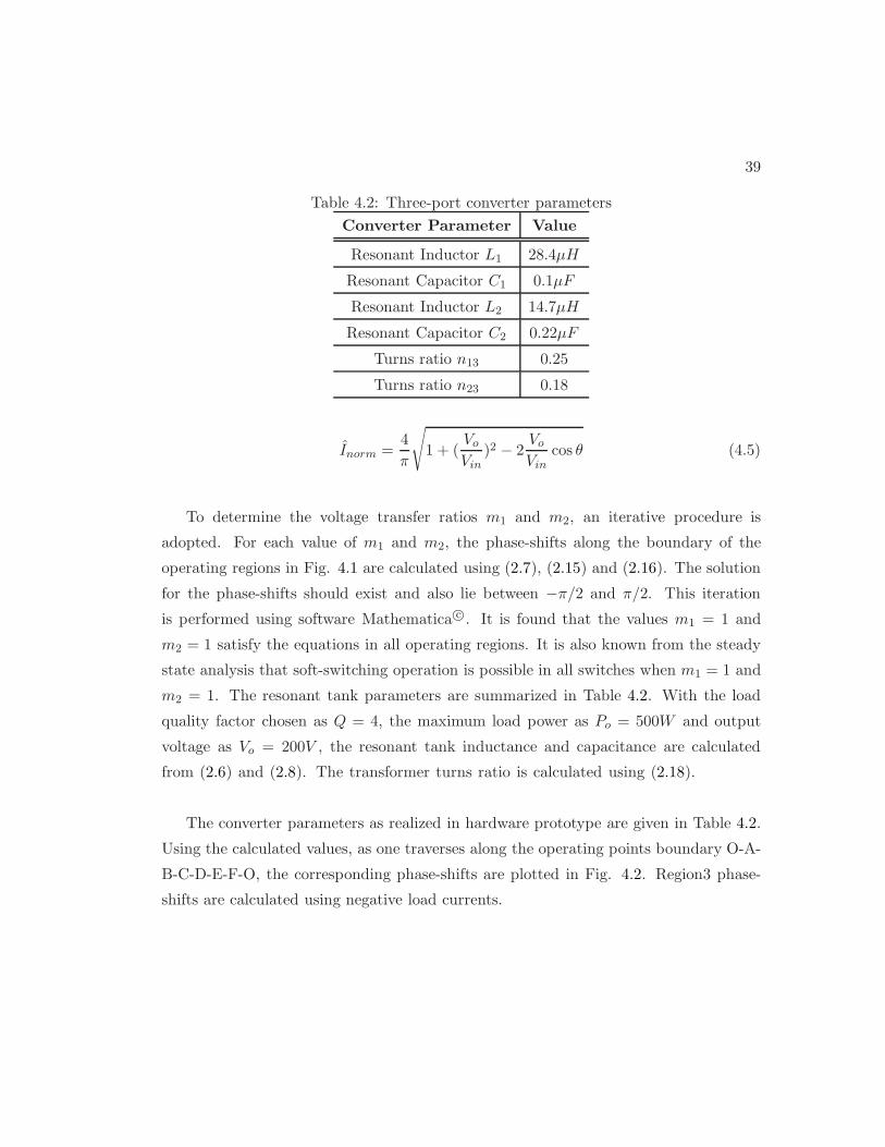
39
Table 4.2: Three-port converter parameters
Converter Parameter Value
Resonant Inductor L1 28.4µH
Resonant Capacitor C1 0.1µF
Resonant Inductor L2 14.7µH
Resonant Capacitor C2 0.22µF
Turns ratio n13 0.25
Turns ratio n23 0.18
Inorm =4
π
√
1 + (Vo
Vin)2 − 2
Vo
Vincos θ (4.5)
To determine the voltage transfer ratios m1 and m2, an iterative procedure is
adopted. For each value of m1 and m2, the phase-shifts along the boundary of the
operating regions in Fig. 4.1 are calculated using (2.7), (2.15) and (2.16). The solution
for the phase-shifts should exist and also lie between −π/2 and π/2. This iteration
is performed using software Mathematica c©. It is found that the values m1 = 1 and
m2 = 1 satisfy the equations in all operating regions. It is also known from the steady
state analysis that soft-switching operation is possible in all switches when m1 = 1 and
m2 = 1. The resonant tank parameters are summarized in Table 4.2. With the load
quality factor chosen as Q = 4, the maximum load power as Po = 500W and output
voltage as Vo = 200V , the resonant tank inductance and capacitance are calculated
from (2.6) and (2.8). The transformer turns ratio is calculated using (2.18).
The converter parameters as realized in hardware prototype are given in Table 4.2.
Using the calculated values, as one traverses along the operating points boundary O-A-
B-C-D-E-F-O, the corresponding phase-shifts are plotted in Fig. 4.2. Region3 phase-
shifts are calculated using negative load currents.
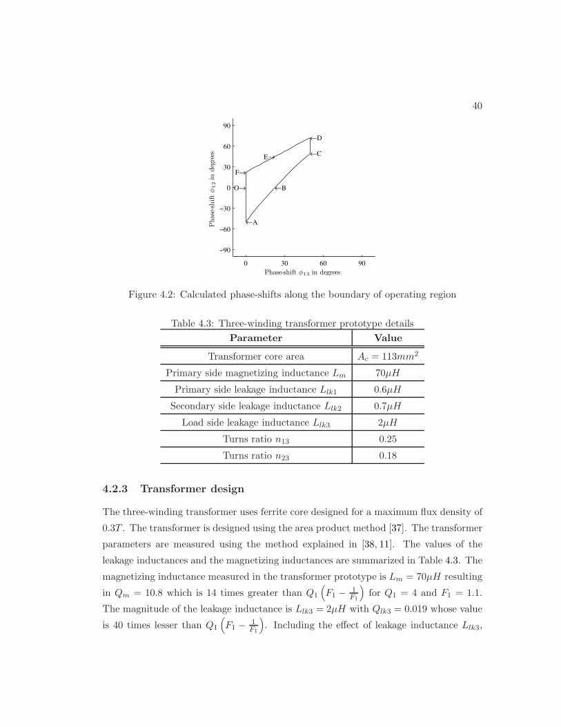
40
0 30 60 90
−90
−60
−30
0
30
60
90
Phase-shift φ13 in degrees
Phas
e-sh
ift
φ12
indeg
rees
←A
←B
←C
←D
E→
F→
O→
Figure 4.2: Calculated phase-shifts along the boundary of operating region
Table 4.3: Three-winding transformer prototype details
Parameter Value
Transformer core area Ac = 113mm2
Primary side magnetizing inductance Lm 70µH
Primary side leakage inductance Llk1 0.6µH
Secondary side leakage inductance Llk2 0.7µH
Load side leakage inductance Llk3 2µH
Turns ratio n13 0.25
Turns ratio n23 0.18
4.2.3 Transformer design
The three-winding transformer uses ferrite core designed for a maximum flux density of
0.3T . The transformer is designed using the area product method [37]. The transformer
parameters are measured using the method explained in [38, 11]. The values of the
leakage inductances and the magnetizing inductances are summarized in Table 4.3. The
magnetizing inductance measured in the transformer prototype is Lm = 70µH resulting
in Qm = 10.8 which is 14 times greater than Q1
(
F1 − 1F1
)
for Q1 = 4 and F1 = 1.1.
The magnitude of the leakage inductance is Llk3 = 2µH with Qlk3 = 0.019 whose value
is 40 times lesser than Q1
(
F1 − 1F1
)
. Including the effect of leakage inductance Llk3,
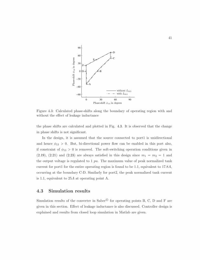
41
0 30 60 90
−90
−60
−30
0
30
60
90
Phase-shift φ13 in degrees
Phas
e-sh
ift
φ12
indeg
rees
←A
←B
←C
←D
E→
F→
O→
without Llk3
with Llk3
Figure 4.3: Calculated phase-shifts along the boundary of operating region with andwithout the effect of leakage inductance
the phase shifts are calculated and plotted in Fig. 4.3. It is observed that the change
in phase shifts is not significant.
In the design, it is assumed that the source connected to port1 is unidirectional
and hence φ13 > 0. But, bi-directional power flow can be enabled in this port also,
if constraint of φ13 > 0 is removed. The soft-switching operation conditions given in
(2.19), (2.21) and (2.23) are always satisfied in this design since m1 = m2 = 1 and
the output voltage is regulated to 1 pu. The maximum value of peak normalized tank
current for port1 for the entire operating region is found to be 1.1, equivalent to 17.8A,
occurring at the boundary C-D. Similarly for port2, the peak normalized tank current
is 1.1, equivalent to 25A at operating point A.
4.3 Simulation results
Simulation results of the converter in Saber c© for operating points B, C, D and F are
given in this section. Effect of leakage inductance is also discussed. Controller design is
explained and results from closed loop simulation in Matlab are given.
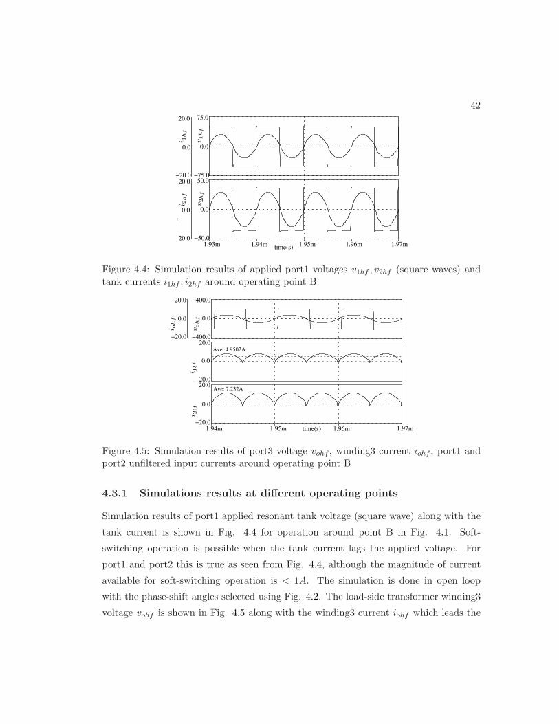
42
(V
)
−50.0
0.0
50.0
time(s)1.93m 1.94m 1.95m 1.96m 1.97m
−75.0
0.0
75.0
−20.0
0.0
20.0
0.0
20.0
20.0
v2h
fv1h
f
i 1h
fi 2
hf
Figure 4.4: Simulation results of applied port1 voltages v1hf , v2hf (square waves) andtank currents i1hf , i2hf around operating point B
−20.0
0.0
20.0
time(s)1.94m 1.95m 1.96m 1.97m
−20.0
0.0
20.0−400.0
0.0
400.0
−20.0
0.0
20.0
Ave: 4.9502A
Ave: 7.232A
i 1lf
voh
fi 2
lf
i oh
f
Figure 4.5: Simulation results of port3 voltage vohf , winding3 current iohf , port1 andport2 unfiltered input currents around operating point B
4.3.1 Simulations results at different operating points
Simulation results of port1 applied resonant tank voltage (square wave) along with the
tank current is shown in Fig. 4.4 for operation around point B in Fig. 4.1. Soft-
switching operation is possible when the tank current lags the applied voltage. For
port1 and port2 this is true as seen from Fig. 4.4, although the magnitude of current
available for soft-switching operation is < 1A. The simulation is done in open loop
with the phase-shift angles selected using Fig. 4.2. The load-side transformer winding3
voltage vohf is shown in Fig. 4.5 along with the winding3 current iohf which leads the
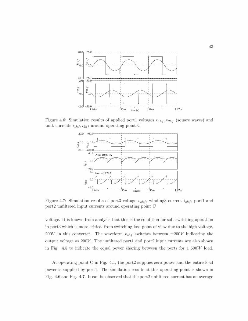
43
−50.0
0.0
50.0
time(s)1.94m 1.95m 1.96m 1.97m−2.0
0.0
2.0−75.0
0.0
75.0
−40.0
0.0
40.0
v1h
fv2h
f
i 2h
fi 1
hf
Figure 4.6: Simulation results of applied port1 voltages v1hf , v2hf (square waves) andtank currents i1hf , i2hf around operating point C
−1.0
0.0
1.0
time(s)1.94m 1.95m 1.96m 1.97m
−40.0
0.0
40.0−400.0
0.0
400.0
−20.0
0.0
20.0
Ave: 10.091A
Ave: −0.178A
i 2lf
i 1lf
voh
f
i oh
f
Figure 4.7: Simulation results of port3 voltage vohf , winding3 current iohf , port1 andport2 unfiltered input currents around operating point C
voltage. It is known from analysis that this is the condition for soft-switching operation
in port3 which is more critical from switching loss point of view due to the high voltage,
200V in this converter. The waveform vohf switches between ±200V indicating the
output voltage as 200V . The unfiltered port1 and port2 input currents are also shown
in Fig. 4.5 to indicate the equal power sharing between the ports for a 500W load.
At operating point C in Fig. 4.1, the port2 supplies zero power and the entire load
power is supplied by port1. The simulation results at this operating point is shown in
Fig. 4.6 and Fig. 4.7. It can be observed that the port2 unfiltered current has an average
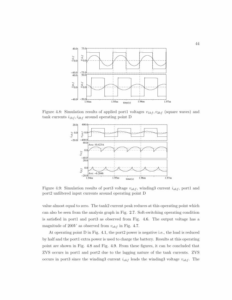
44
−50.0
0.0
50.0
time(s)1.94m 1.95m 1.96m 1.97m−40.0
0.0
40.0−75.0
0.0
75.0
−40.0
0.0
40.0
i 1h
f
v2h
fv1h
f
i 2h
f
Figure 4.8: Simulation results of applied port1 voltages v1hf , v2hf (square waves) andtank currents i1hf , i2hf around operating point D
−20.0
0.0
20.0
time(s)1.94m 1.95m 1.96m 1.97m
−40.0
0.0
40.0−400.0
0.0
400.0
−20.0
0.0
20.0
Ave: 10.423A
Ave: −6.2846i 2lf
voh
fi 1
lf
i oh
f
Figure 4.9: Simulation results of port3 voltage vohf , winding3 current iohf , port1 andport2 unfiltered input currents around operating point D
value almost equal to zero. The tank2 current peak reduces at this operating point which
can also be seen from the analysis graph in Fig. 2.7. Soft-switching operating condition
is satisfied in port1 and port3 as observed from Fig. 4.6. The output voltage has a
magnitude of 200V as observed from vohf in Fig. 4.7.
At operating point D in Fig. 4.1, the port2 power is negative i.e., the load is reduced
by half and the port1 extra power is used to charge the battery. Results at this operating
point are shown in Fig. 4.8 and Fig. 4.9. From these figures, it can be concluded that
ZVS occurs in port1 and port2 due to the lagging nature of the tank currents. ZVS
occurs in port3 since the winding3 current iohf leads the winding3 voltage vohf . The
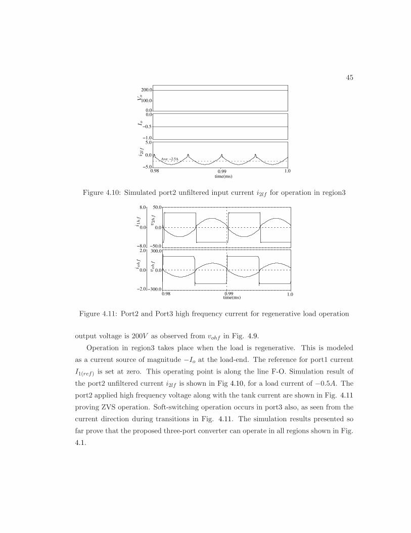
45
Ave: −2.5A
0.99 1.0time(ms)
200.0
100.0
0.00.0
−0.5
−1.0
0.0
5.0
−5.00.98
Vo
i 2lf
Io
Figure 4.10: Simulated port2 unfiltered input current i2lf for operation in region3
0.0
0.98time(ms)0.99 1.0
8.0
0.0
−8.02.0
0.0
−2.0
50.0
0.0
−50.0300.0
−300.0
i 1h
fi o
hf
v2h
fv
oh
f
Figure 4.11: Port2 and Port3 high frequency current for regenerative load operation
output voltage is 200V as observed from vohf in Fig. 4.9.
Operation in region3 takes place when the load is regenerative. This is modeled
as a current source of magnitude −Io at the load-end. The reference for port1 current
I1(ref) is set at zero. This operating point is along the line F-O. Simulation result of
the port2 unfiltered current i2lf is shown in Fig 4.10, for a load current of −0.5A. The
port2 applied high frequency voltage along with the tank current are shown in Fig. 4.11
proving ZVS operation. Soft-switching operation occurs in port3 also, as seen from the
current direction during transitions in Fig. 4.11. The simulation results presented so
far prove that the proposed three-port converter can operate in all regions shown in Fig.
4.1.
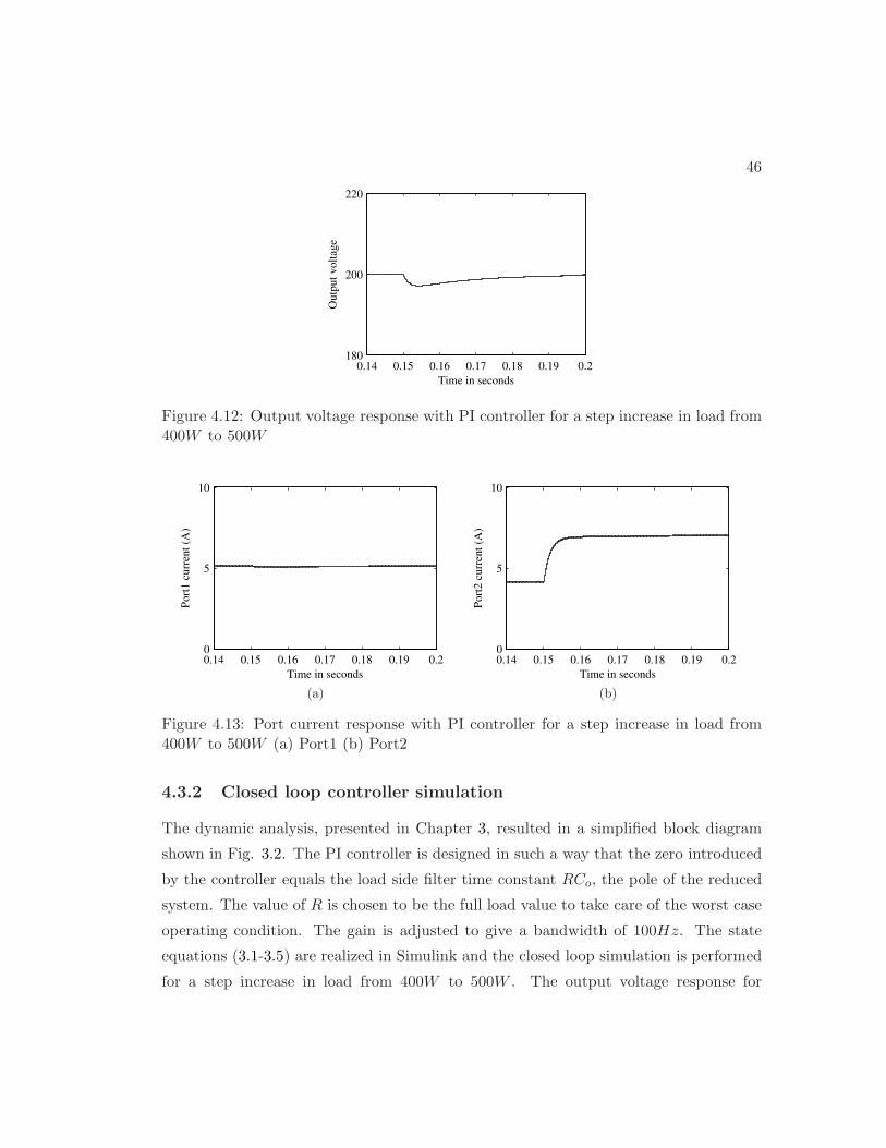
46
0.14 0.15 0.16 0.17 0.18 0.19 0.2180
200
220
Time in seconds
Outp
ut
volt
age
Figure 4.12: Output voltage response with PI controller for a step increase in load from400W to 500W
0.14 0.15 0.16 0.17 0.18 0.19 0.20
5
10
Time in seconds
Port
1 c
urr
ent
(A)
(a)
0.14 0.15 0.16 0.17 0.18 0.19 0.20
5
10
Time in seconds
Port
2 c
urr
ent
(A)
(b)
Figure 4.13: Port current response with PI controller for a step increase in load from400W to 500W (a) Port1 (b) Port2
4.3.2 Closed loop controller simulation
The dynamic analysis, presented in Chapter 3, resulted in a simplified block diagram
shown in Fig. 3.2. The PI controller is designed in such a way that the zero introduced
by the controller equals the load side filter time constant RCo, the pole of the reduced
system. The value of R is chosen to be the full load value to take care of the worst case
operating condition. The gain is adjusted to give a bandwidth of 100Hz. The state
equations (3.1-3.5) are realized in Simulink and the closed loop simulation is performed
for a step increase in load from 400W to 500W . The output voltage response for
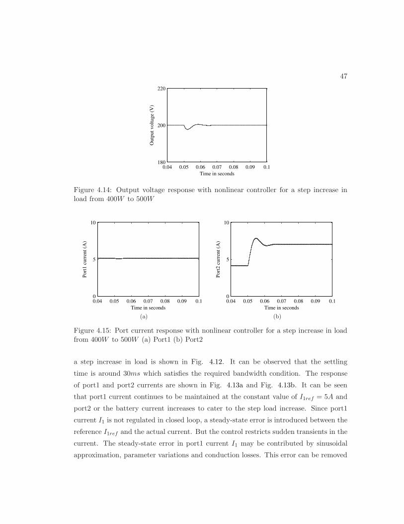
47
0.04 0.05 0.06 0.07 0.08 0.09 0.1180
200
220
Time in seconds
Outp
ut
volt
age
(V)
Figure 4.14: Output voltage response with nonlinear controller for a step increase inload from 400W to 500W
0.04 0.05 0.06 0.07 0.08 0.09 0.10
5
10
Time in seconds
Port
1 c
urr
ent
(A)
(a)
0.04 0.05 0.06 0.07 0.08 0.09 0.10
5
10
Time in seconds
Port
2 c
urr
ent
(A)
(b)
Figure 4.15: Port current response with nonlinear controller for a step increase in loadfrom 400W to 500W (a) Port1 (b) Port2
a step increase in load is shown in Fig. 4.12. It can be observed that the settling
time is around 30ms which satisfies the required bandwidth condition. The response
of port1 and port2 currents are shown in Fig. 4.13a and Fig. 4.13b. It can be seen
that port1 current continues to be maintained at the constant value of I1ref = 5A and
port2 or the battery current increases to cater to the step load increase. Since port1
current I1 is not regulated in closed loop, a steady-state error is introduced between the
reference I1ref and the actual current. But the control restricts sudden transients in the
current. The steady-state error in port1 current I1 may be contributed by sinusoidal
approximation, parameter variations and conduction losses. This error can be removed

48
S2
vc1
vc3
vc2
Ts
2
φ13
φ12
t
t
t
S3
S1
Figure 4.16: Carrier signal and control voltages for generating the PWM pulses for thethree-port converter
by adding another slow control loop to regulate the port1 current.
A non-linear controller is designed as explained in Section 3.5 to compare the re-
sponse with the PI controller. In the equations, R is unknown and it is estimated in the
control loop. The results of the 100W step increase in load are given in Fig. 4.14 and
Fig. 4.15. The values of g and k are chosen to have the dominant pole at 2π100 rad/s.
4.4 Experimental results
4.4.1 Laboratory setup
A 500W prototype is realized in hardware with the controller implemented in Digilent
Basys c© FPGA board [39]. The pulses for the Mosfets are generated using a ramp carrier
signal and two control voltages for the two phase-shifts as shown in Fig. 4.16. The pulse
generation module is also implemented in FPGA. Since all the pulses are at 50%, pulse
transformers are used for isolation in gate-drive. The converter parameters are given
in Table 4.2. The battery port has three 12V, 12Ah lead acid batteries connected in
series. Port1 uses a dc source with magnitude 50V , to emulate a renewable energy
source. The output voltage is sensed using an LEM sensor whose output is connected
to an ADC module with the FPGA. The converter operates in closed loop with output
voltage regulated at 200V . The closed loop controller design is explained in the previous
section. The hardware setup for testing is shown in Fig. 4.17.
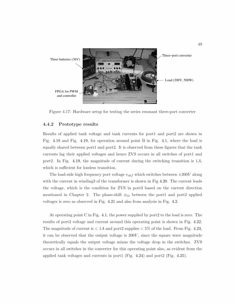
49
Three batteries (36V)Three−port converter
Load (200V, 500W)
FPGA for PWM
and controller
Figure 4.17: Hardware setup for testing the series resonant three-port converter
4.4.2 Prototype results
Results of applied tank voltage and tank currents for port1 and port2 are shown in
Fig. 4.18 and Fig. 4.19, for operation around point B in Fig. 4.1, where the load is
equally shared between port1 and port2. It is observed from these figures that the tank
currents lag their applied voltages and hence ZVS occurs in all switches of port1 and
port2. In Fig. 4.19, the magnitude of current during the switching transition is 1A,
which is sufficient for lossless transition.
The load-side high frequency port voltage vohf which switches between ±200V along
with the current in winding3 of the transformer is shown in Fig 4.20. The current leads
the voltage, which is the condition for ZVS in port3 based on the current direction
mentioned in Chapter 2. The phase-shift φ12 between the port1 and port2 applied
voltages is zero as observed in Fig. 4.21 and also from analysis in Fig. 4.2.
At operating point C in Fig. 4.1, the power supplied by port2 to the load is zero. The
results of port2 voltage and current around this operating point is shown in Fig. 4.22.
The magnitude of current is < 1A and port2 supplies < 5% of the load. From Fig. 4.23,
it can be observed that the output voltage is 200V , since the square wave magnitude
theoretically equals the output voltage minus the voltage drop in the switches. ZVS
occurs in all switches in the converter for this operating point also, as evident from the
applied tank voltages and currents in port1 (Fig. 4.24) and port2 (Fig. 4.25).
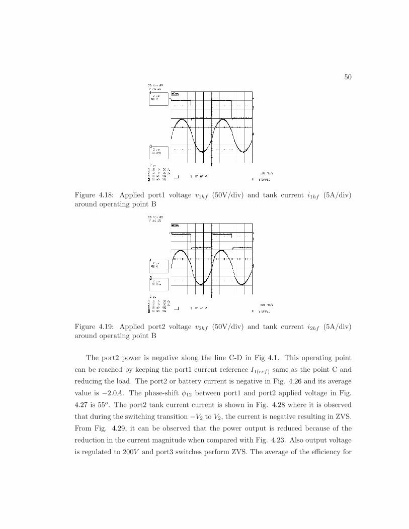
50
Figure 4.18: Applied port1 voltage v1hf (50V/div) and tank current i1hf (5A/div)around operating point B
Figure 4.19: Applied port2 voltage v2hf (50V/div) and tank current i2hf (5A/div)around operating point B
The port2 power is negative along the line C-D in Fig 4.1. This operating point
can be reached by keeping the port1 current reference I1(ref) same as the point C and
reducing the load. The port2 or battery current is negative in Fig. 4.26 and its average
value is −2.0A. The phase-shift φ12 between port1 and port2 applied voltage in Fig.
4.27 is 55o. The port2 tank current current is shown in Fig. 4.28 where it is observed
that during the switching transition −V2 to V2, the current is negative resulting in ZVS.
From Fig. 4.29, it can be observed that the power output is reduced because of the
reduction in the current magnitude when compared with Fig. 4.23. Also output voltage
is regulated to 200V and port3 switches perform ZVS. The average of the efficiency for
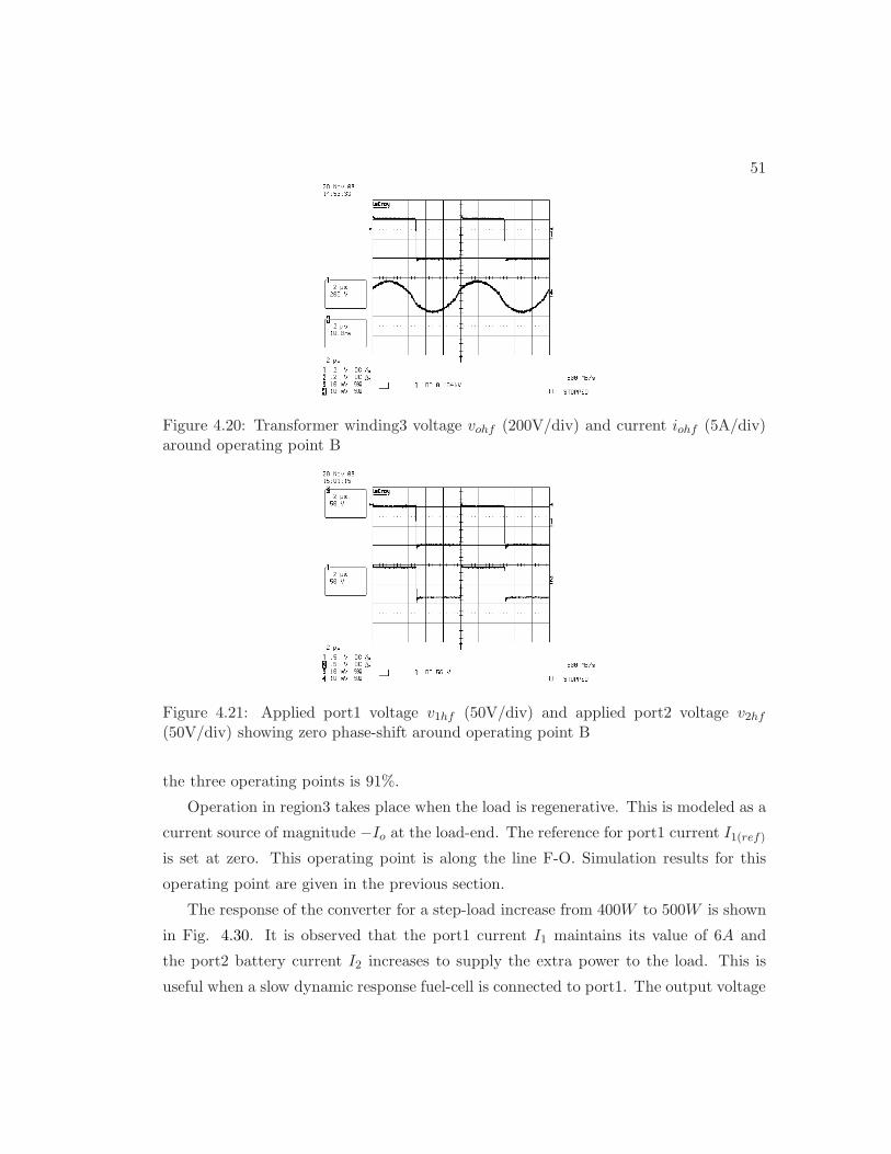
51
Figure 4.20: Transformer winding3 voltage vohf (200V/div) and current iohf (5A/div)around operating point B
Figure 4.21: Applied port1 voltage v1hf (50V/div) and applied port2 voltage v2hf
(50V/div) showing zero phase-shift around operating point B
the three operating points is 91%.
Operation in region3 takes place when the load is regenerative. This is modeled as a
current source of magnitude −Io at the load-end. The reference for port1 current I1(ref)
is set at zero. This operating point is along the line F-O. Simulation results for this
operating point are given in the previous section.
The response of the converter for a step-load increase from 400W to 500W is shown
in Fig. 4.30. It is observed that the port1 current I1 maintains its value of 6A and
the port2 battery current I2 increases to supply the extra power to the load. This is
useful when a slow dynamic response fuel-cell is connected to port1. The output voltage

52
Figure 4.22: Port2 dc voltage V2 (50V/div) and dc current I2 (2A/div) around operatingpoint C
Figure 4.23: Transformer winding3 voltage vohf (200V/div) and current iohf (5A/div)around operating point C
settles back to its original value after 30ms as seen from the response. The designed
bandwidth is low due to hardware implementation constraints.
4.5 Comparison with existing three-port converter
The proposed series resonant based triple active bridge (TABSRC) three-port dc-dc
converter Fig. 2.2 is compared with a triple active bridge converter (TAB) with induc-
tors only Fig. 1.4. A 2.5kW power converter is designed using both types of converter
circuits. A power level of 2.5kW is chosen to meet the typical peak power demand in a
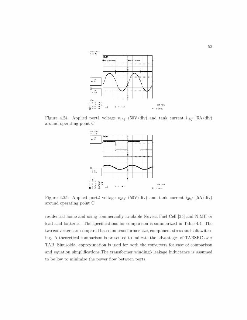
53
Figure 4.24: Applied port1 voltage v1hf (50V/div) and tank current i1hf (5A/div)around operating point C
Figure 4.25: Applied port2 voltage v2hf (50V/div) and tank current i2hf (5A/div)around operating point C
residential home and using commercially available Nuvera Fuel Cell [35] and NiMH or
lead acid batteries. The specifications for comparison is summarized in Table 4.4. The
two converters are compared based on transformer size, component stress and softswitch-
ing. A theoretical comparison is presented to indicate the advantages of TABSRC over
TAB. Sinusoidal approximation is used for both the converters for ease of comparison
and equation simplifications.The transformer winding3 leakage inductance is assumed
to be low to minimize the power flow between ports.
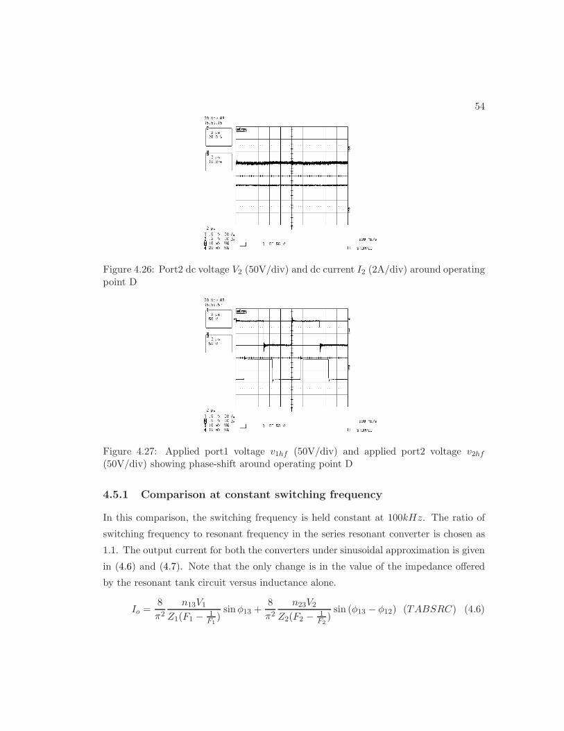
54
Figure 4.26: Port2 dc voltage V2 (50V/div) and dc current I2 (2A/div) around operatingpoint D
Figure 4.27: Applied port1 voltage v1hf (50V/div) and applied port2 voltage v2hf
(50V/div) showing phase-shift around operating point D
4.5.1 Comparison at constant switching frequency
In this comparison, the switching frequency is held constant at 100kHz. The ratio of
switching frequency to resonant frequency in the series resonant converter is chosen as
1.1. The output current for both the converters under sinusoidal approximation is given
in (4.6) and (4.7). Note that the only change is in the value of the impedance offered
by the resonant tank circuit versus inductance alone.
Io =8
π2
n13V1
Z1(F1 − 1F1
)sinφ13 +
8
π2
n23V2
Z2(F2 − 1F2
)sin (φ13 − φ12) (TABSRC) (4.6)
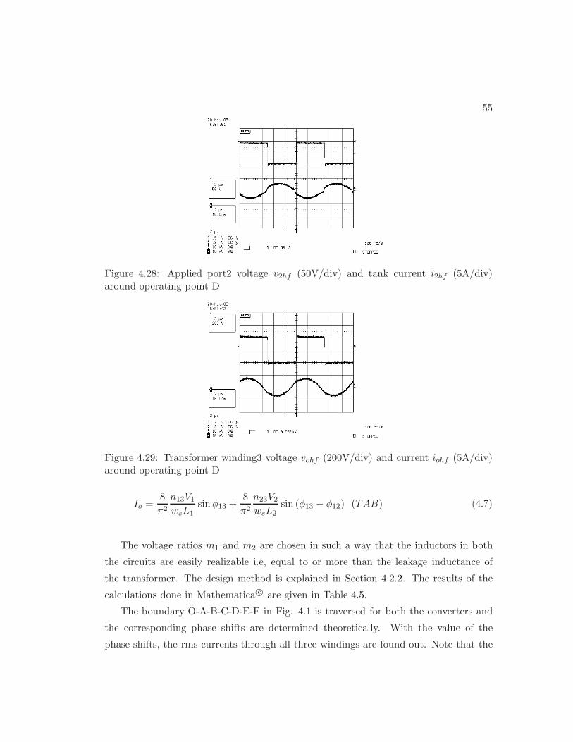
55
Figure 4.28: Applied port2 voltage v2hf (50V/div) and tank current i2hf (5A/div)around operating point D
Figure 4.29: Transformer winding3 voltage vohf (200V/div) and current iohf (5A/div)around operating point D
Io =8
π2
n13V1
wsL1sin φ13 +
8
π2
n23V2
wsL2sin (φ13 − φ12) (TAB) (4.7)
The voltage ratios m1 and m2 are chosen in such a way that the inductors in both
the circuits are easily realizable i.e, equal to or more than the leakage inductance of
the transformer. The design method is explained in Section 4.2.2. The results of the
calculations done in Mathematica c© are given in Table 4.5.
The boundary O-A-B-C-D-E-F in Fig. 4.1 is traversed for both the converters and
the corresponding phase shifts are determined theoretically. With the value of the
phase shifts, the rms currents through all three windings are found out. Note that the
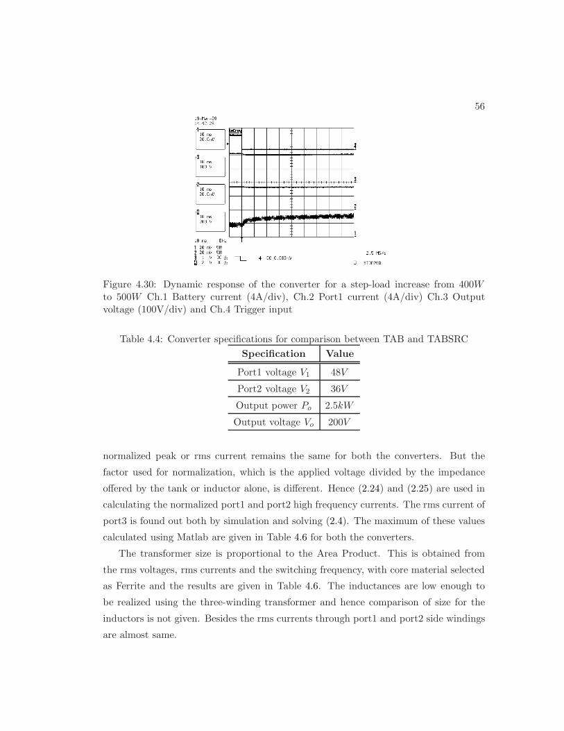
56
Figure 4.30: Dynamic response of the converter for a step-load increase from 400Wto 500W Ch.1 Battery current (4A/div), Ch.2 Port1 current (4A/div) Ch.3 Outputvoltage (100V/div) and Ch.4 Trigger input
Table 4.4: Converter specifications for comparison between TAB and TABSRC
Specification Value
Port1 voltage V1 48V
Port2 voltage V2 36V
Output power Po 2.5kW
Output voltage Vo 200V
normalized peak or rms current remains the same for both the converters. But the
factor used for normalization, which is the applied voltage divided by the impedance
offered by the tank or inductor alone, is different. Hence (2.24) and (2.25) are used in
calculating the normalized port1 and port2 high frequency currents. The rms current of
port3 is found out both by simulation and solving (2.4). The maximum of these values
calculated using Matlab are given in Table 4.6 for both the converters.
The transformer size is proportional to the Area Product. This is obtained from
the rms voltages, rms currents and the switching frequency, with core material selected
as Ferrite and the results are given in Table 4.6. The inductances are low enough to
be realized using the three-winding transformer and hence comparison of size for the
inductors is not given. Besides the rms currents through port1 and port2 side windings
are almost same.
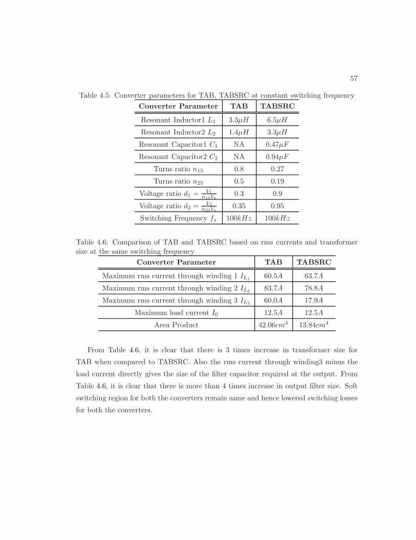
57
Table 4.5: Converter parameters for TAB, TABSRC at constant switching frequency
Converter Parameter TAB TABSRC
Resonant Inductor1 L1 3.3µH 6.5µH
Resonant Inductor2 L2 1.4µH 3.3µH
Resonant Capacitor1 C1 NA 0.47µF
Resonant Capacitor2 C2 NA 0.94µF
Turns ratio n13 0.8 0.27
Turns ratio n23 0.5 0.19
Voltage ratio d1 = V1n13Vo
0.3 0.9
Voltage ratio d2 = V2n23Vo
0.35 0.95
Switching Frequency fs 100kHz 100kHz
Table 4.6: Comparison of TAB and TABSRC based on rms currents and transformersize at the same switching frequency
Converter Parameter TAB TABSRC
Maximum rms current through winding 1 IL1 60.5A 63.7A
Maximum rms current through winding 2 IL2 83.7A 78.8A
Maximum rms current through winding 3 IL3 60.0A 17.9A
Maximum load current I0 12.5A 12.5A
Area Product 42.06cm4 13.84cm4
From Table 4.6, it is clear that there is 3 times increase in transformer size for
TAB when compared to TABSRC. Also the rms current through winding3 minus the
load current directly gives the size of the filter capacitor required at the output. From
Table 4.6, it is clear that there is more than 4 times increase in output filter size. Soft
switching region for both the converters remain same and hence lowered switching losses
for both the converters.
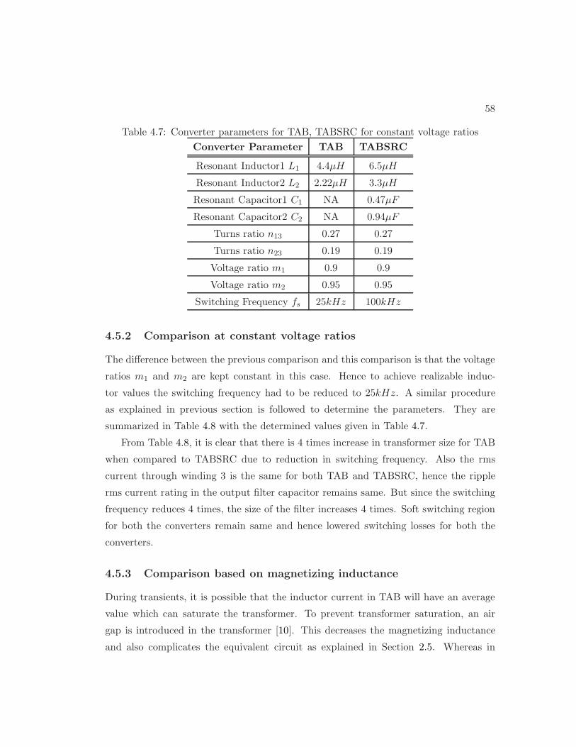
58
Table 4.7: Converter parameters for TAB, TABSRC for constant voltage ratios
Converter Parameter TAB TABSRC
Resonant Inductor1 L1 4.4µH 6.5µH
Resonant Inductor2 L2 2.22µH 3.3µH
Resonant Capacitor1 C1 NA 0.47µF
Resonant Capacitor2 C2 NA 0.94µF
Turns ratio n13 0.27 0.27
Turns ratio n23 0.19 0.19
Voltage ratio m1 0.9 0.9
Voltage ratio m2 0.95 0.95
Switching Frequency fs 25kHz 100kHz
4.5.2 Comparison at constant voltage ratios
The difference between the previous comparison and this comparison is that the voltage
ratios m1 and m2 are kept constant in this case. Hence to achieve realizable induc-
tor values the switching frequency had to be reduced to 25kHz. A similar procedure
as explained in previous section is followed to determine the parameters. They are
summarized in Table 4.8 with the determined values given in Table 4.7.
From Table 4.8, it is clear that there is 4 times increase in transformer size for TAB
when compared to TABSRC due to reduction in switching frequency. Also the rms
current through winding 3 is the same for both TAB and TABSRC, hence the ripple
rms current rating in the output filter capacitor remains same. But since the switching
frequency reduces 4 times, the size of the filter increases 4 times. Soft switching region
for both the converters remain same and hence lowered switching losses for both the
converters.
4.5.3 Comparison based on magnetizing inductance
During transients, it is possible that the inductor current in TAB will have an average
value which can saturate the transformer. To prevent transformer saturation, an air
gap is introduced in the transformer [10]. This decreases the magnetizing inductance
and also complicates the equivalent circuit as explained in Section 2.5. Whereas in
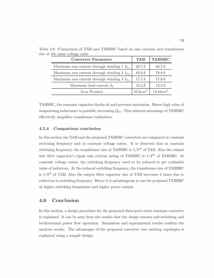
59
Table 4.8: Comparison of TAB and TABSRC based on rms currents and transformersize at the same voltage ratio
Converter Parameter TAB TABSRC
Maximum rms current through winding 1 IL1 62.7A 63.7A
Maximum rms current through winding 2 IL2 83.9A 78.8A
Maximum rms current through winding 3 IL3 17.7A 17.9A
Maximum load current I0 12.5A 12.5A
Area Product 55.6cm4 13.84cm4
TABSRC, the resonant capacitor blocks dc and prevents saturation. Hence high value of
magnetizing inductance is possible, increasing Qm. This inherent advantage of TABSRC
effectively simplifies transformer realization.
4.5.4 Comparison conclusion
In this section the TAB and the proposed TABSRC converters are compared at constant
switching frequency and at constant voltage ratios. It is observed that at constant
switching frequency, the transformer size of TABSRC is 1/3rd of TAB. Also the output
side filter capacitor’s ripple rms current rating of TABSRC is 1/4th of TABSRC. At
constant voltage ratios, the switching frequency need to be reduced to get realizable
value of inductors. At the reduced switching frequency, the transformer size of TABSRC
is 1/4th of TAB. Also the output filter capacitor size of TAB increases 4 times due to
reduction in switching frequency. Hence it is advantageous to use the proposed TABSRC
at higher switching frequencies and higher power output.
4.6 Conclusion
In this section, a design procedure for the proposed three-port series resonant converter
is explained. It can be seen from the results that the design ensures soft-switching and
bi-directional power flow operation. Simulation and experimental results confirm the
analysis results. The advantages of the proposed converter over existing topologies is
explained using a sample design.
Chapter 5
Three-port Series Resonant
Converter - Load-side Diode
Bridge
The active bridge in the proposed three-port series resonant converter can be replaced
by a diode bridge for uni-directional load applications. This is useful in reducing the
switching losses in the load-side converter especially at loads less than 50% of the maxi-
mum load and at very high output voltages. It also reduces the drive circuitry necessary
for the load-side active bridge if application does not demand regenerative load capa-
bility. Load-side diode bridge is more economical in such applications. In this Chapter,
phase-shift modulation (PSM) control techniques are proposed for the three-port series
resonant converter with load-side diode bridge. Analysis, simulation and experimental
results are presented.
5.1 Proposed topology and modulation schemes
The series resonant three-port converter with load-side diode bridge is shown in Fig.
5.1. Port1 can be a Fuel cell or any constant dc power source and port2 is shown as
Battery. L1 and C1 form the resonant tank circuit for port1 and L2 and C2 for port2.
Capacitors Cf1 and Cf2 form the filter capacitors at the input of each of the ports. The
60
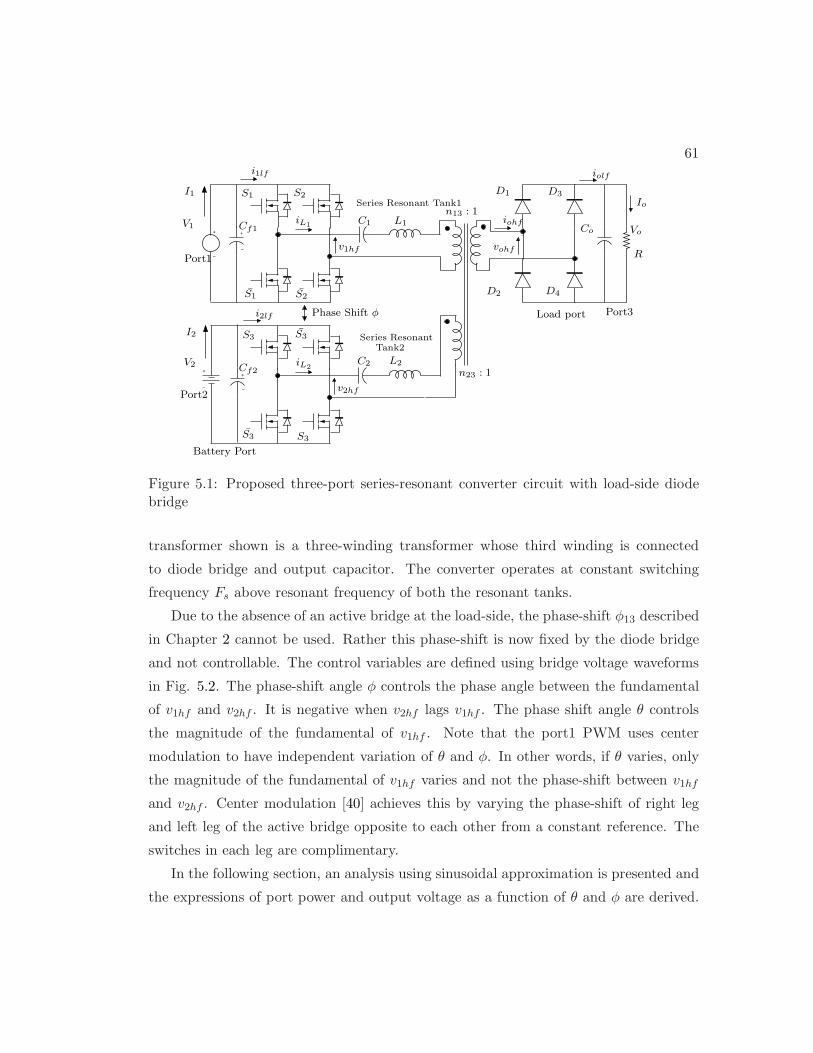
61
−
+
+
−
+
−
+
−
iohf
I1
I2
D1 D3
D4
C1
RPort1
Battery Port
V1
V2
i1lf
i2lf Phase Shift φ
Series Resonant Tank1
Load port
Io
L1Cf1
Cf2
iL1
D2S2
S2
Series Resonant
Tank2
Port2
iL2
Port3
n13 : 1
vohf
Co
S1
Vo
iolf
v1hf
S3 S3
v2hf
L2C2
S3S3
S1
n23 : 1
Figure 5.1: Proposed three-port series-resonant converter circuit with load-side diodebridge
transformer shown is a three-winding transformer whose third winding is connected
to diode bridge and output capacitor. The converter operates at constant switching
frequency Fs above resonant frequency of both the resonant tanks.
Due to the absence of an active bridge at the load-side, the phase-shift φ13 described
in Chapter 2 cannot be used. Rather this phase-shift is now fixed by the diode bridge
and not controllable. The control variables are defined using bridge voltage waveforms
in Fig. 5.2. The phase-shift angle φ controls the phase angle between the fundamental
of v1hf and v2hf . It is negative when v2hf lags v1hf . The phase shift angle θ controls
the magnitude of the fundamental of v1hf . Note that the port1 PWM uses center
modulation to have independent variation of θ and φ. In other words, if θ varies, only
the magnitude of the fundamental of v1hf varies and not the phase-shift between v1hf
and v2hf . Center modulation [40] achieves this by varying the phase-shift of right leg
and left leg of the active bridge opposite to each other from a constant reference. The
switches in each leg are complimentary.
In the following section, an analysis using sinusoidal approximation is presented and
the expressions of port power and output voltage as a function of θ and φ are derived.
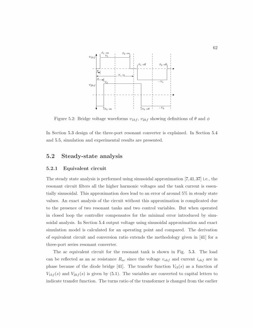
62
S3 off
S1 off S2 off
S3 on
v1hf
V2−V1
−V2
θ
φ
Ts/2
v2hf
V1
S1 on S2 on
Figure 5.2: Bridge voltage waveforms v1hf , v2hf showing definitions of θ and φ
In Section 5.3 design of the three-port resonant converter is explained. In Section 5.4
and 5.5, simulation and experimental results are presented.
5.2 Steady-state analysis
5.2.1 Equivalent circuit
The steady state analysis is performed using sinusoidal approximation [7,41,37] i.e., the
resonant circuit filters all the higher harmonic voltages and the tank current is essen-
tially sinusoidal. This approximation does lead to an error of around 5% in steady state
values. An exact analysis of the circuit without this approximation is complicated due
to the presence of two resonant tanks and two control variables. But when operated
in closed loop the controller compensates for the minimal error introduced by sinu-
soidal analysis. In Section 5.4 output voltage using sinusoidal approximation and exact
simulation model is calculated for an operating point and compared. The derivation
of equivalent circuit and conversion ratio extends the methodology given in [41] for a
three-port series resonant converter.
The ac equivalent circuit for the resonant tank is shown in Fig. 5.3. The load
can be reflected as an ac resistance Rac since the voltage vohf and current iohf are in
phase because of the diode bridge [41]. The transfer function Vt3(s) as a function of
V1hf (s) and V2hf (s) is given by (5.1). The variables are converted to capital letters to
indicate transfer function. The turns ratio of the transformer is changed from the earlier

63
V1hf (s)
V1hf (s)Vt1
Vt2
Vt3
C1
C2
L1
L2
Rac
Three-WindingTransformer
n2 : n3
Rac = 8π2 R
I1hf
I2hf
n1 : n3
Figure 5.3: AC equivalent circuit of the resonant tank network for analysis
converter to distinguish the final steady-state expressions.
Vt3(s) = H1(s)n3
n1V1hf (s) + H2(s)
n3
n2V2hf (s) (5.1)
The quality factor and the ratio of switching frequency Fs to the resonant frequency
are defined in (5.2). ω1 and ω2 are the resonant frequencies in rad/s for resonant tank
1 and 2 respectively.
Fi =ωs
ωi; ωs = 2πFs; ωi =
1√LiCi
; Qi =
√
LiCi
8π2 Rac
(
n2i
n23
) ; i = 1, 2 (5.2)
5.2.2 Steady-state equations
The gain of the transfer functions H1(s) and H2(s) is evaluated at switching frequency
(5.3).
‖Hi(jωs)‖ =
[
(
Fi −1
Fi
)2
Q2i +
1 +QiFj
(
1 − F 2i
)
QjFi
(
1 − F 2j
)
2 ]−0.5
(5.3)
where i = 1, 2; j = 1, 2; i 6= j
The phase shift angle θ changes the magnitude of the fundamental component of
v1hf co-sinusoidally as determined from Fourier series. The phase shift angle φ, which
is the phase difference between the two fundamental sinusoidal components v1hf and

64
v2hf , changes the phase angle of the resultant sine voltage in the second part of (5.1).
In a two port series resonant converter the magnitude of transfer function at switching
frequency directly gives the voltage gain of the converter. The analysis here is done in
a similar way but the effects of both θ and φ have to be included since the currents i1hf
and i2hf are not in phase. After some algebra, the dc output voltage Vo as a function
of input dc voltages V1 and V2 is derived and shown in (5.4).
Vo =[
(
V1n3
n1H1m cos θ
)2
+
(
V2n3
n2H2m
)2
(5.4)
+ 2V1n3
n1H1mV2
n3
n2H2m cos θ cos φ
]0.5
where Him = ‖Hi(jωs)‖; i = 1, 2
The expressions can be converted to per unit representation for ease of calculations,
design and comparison. Let the base voltage be defined as Vb and the base power as Pb.
In design, the values of these are chosen as the required output voltage and the required
output power. The voltage conversion ratios are defined in (5.5).
mi =Vi
(
n3ni
)
Vb
; i = 1, 2 (5.5)
The expression of the output voltage (5.4) can then be converted to per unit as given
in (5.6).
Vo,pu =√
(m1H1m cos θ)2 + (m2H2m)2 + 2m1H1mm2H2m cos θ cos φ (5.6)
The current transfer functions I1hf (s) and I2hf (s) from Fig. 5.3 can be written as
a function of V1hf (s) and V2hf (s) in a form similar to (5.1). Transferring to the dc side
using the magnitude and phase of the corresponding transfer functions expressions, the
per unit power from port1 P1,pu and port2 P2,pu are derived and given in (5.7) and (5.8)
where Po,pu is the output power in per unit.
P1,pu =[
I12mm1m2 cos(I12ph + φ)
+ I11mm21 cos θ cos(I11ph)
]
cos θ Po,pu (5.7)
P2,pu =[
I21mm1m2 cos θ cos(I21ph − φ)
+ I22mm22 cos(I22ph)
]
cos θ Po,pu (5.8)
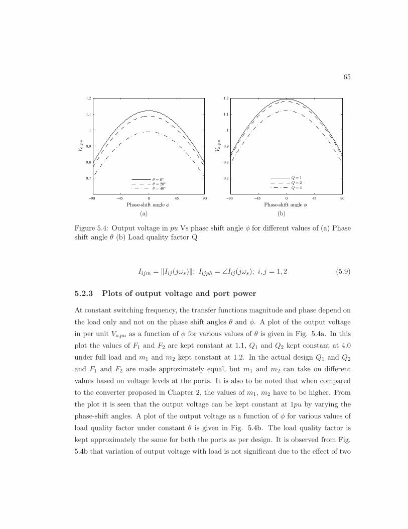
65
−90 −45 0 45 90
0.7
0.8
0.9
1
1.1
1.2
Phase-shift angle φ
Vo
,pu
θ = 0
θ = 20
θ = 40
(a)
−90 −45 0 45 90
0.7
0.8
0.9
1
1.1
1.2
Phase-shift angle φ
Vo
,pu
Q = 1Q = 2Q = 4
(b)
Figure 5.4: Output voltage in pu Vs phase shift angle φ for different values of (a) Phaseshift angle θ (b) Load quality factor Q
Iijm = ‖Iij(jωs)‖; Iijph = ∠Iij(jωs); i, j = 1, 2 (5.9)
5.2.3 Plots of output voltage and port power
At constant switching frequency, the transfer functions magnitude and phase depend on
the load only and not on the phase shift angles θ and φ. A plot of the output voltage
in per unit Vo,pu as a function of φ for various values of θ is given in Fig. 5.4a. In this
plot the values of F1 and F2 are kept constant at 1.1, Q1 and Q2 kept constant at 4.0
under full load and m1 and m2 kept constant at 1.2. In the actual design Q1 and Q2
and F1 and F2 are made approximately equal, but m1 and m2 can take on different
values based on voltage levels at the ports. It is also to be noted that when compared
to the converter proposed in Chapter 2, the values of m1, m2 have to be higher. From
the plot it is seen that the output voltage can be kept constant at 1pu by varying the
phase-shift angles. A plot of the output voltage as a function of φ for various values of
load quality factor under constant θ is given in Fig. 5.4b. The load quality factor is
kept approximately the same for both the ports as per design. It is observed from Fig.
5.4b that variation of output voltage with load is not significant due to the effect of two
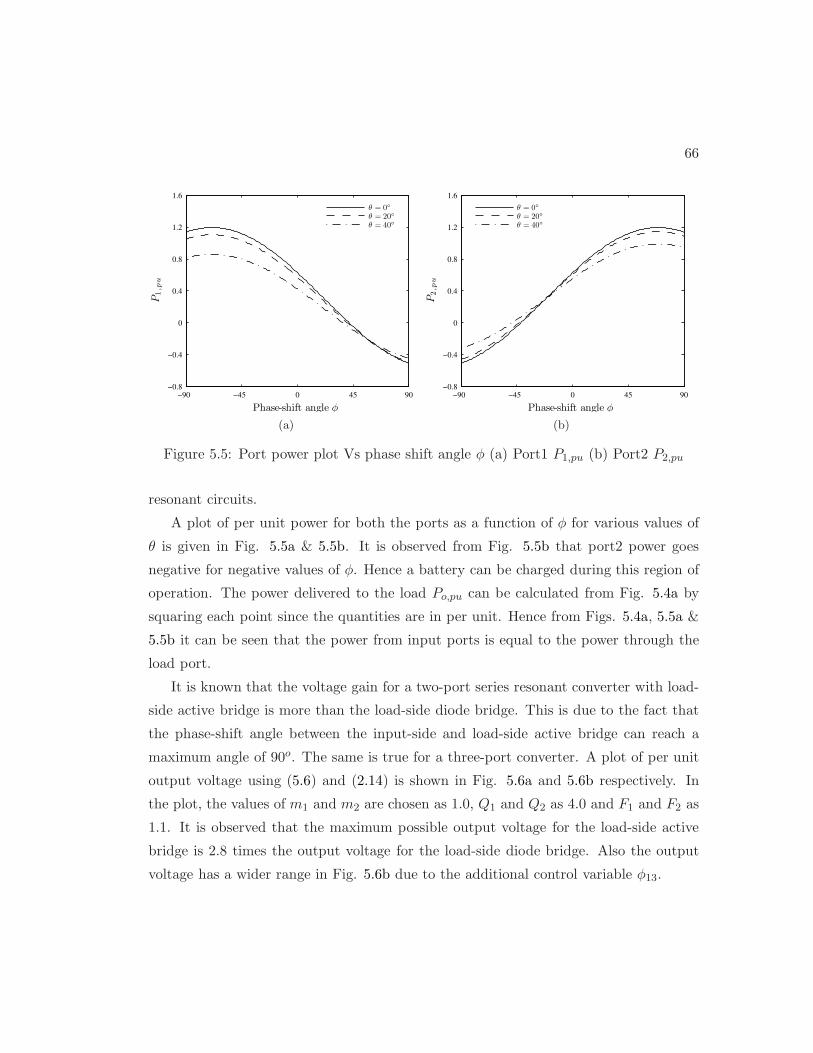
66
−90 −45 0 45 90−0.8
−0.4
0
0.4
0.8
1.2
1.6
Phase-shift angle φ
P1
,pu
θ = 0
θ = 20
θ = 40
(a)
−90 −45 0 45 90−0.8
−0.4
0
0.4
0.8
1.2
1.6
Phase-shift angle φ
P2
,pu
θ = 0
θ = 20
θ = 40
(b)
Figure 5.5: Port power plot Vs phase shift angle φ (a) Port1 P1,pu (b) Port2 P2,pu
resonant circuits.
A plot of per unit power for both the ports as a function of φ for various values of
θ is given in Fig. 5.5a & 5.5b. It is observed from Fig. 5.5b that port2 power goes
negative for negative values of φ. Hence a battery can be charged during this region of
operation. The power delivered to the load Po,pu can be calculated from Fig. 5.4a by
squaring each point since the quantities are in per unit. Hence from Figs. 5.4a, 5.5a &
5.5b it can be seen that the power from input ports is equal to the power through the
load port.
It is known that the voltage gain for a two-port series resonant converter with load-
side active bridge is more than the load-side diode bridge. This is due to the fact that
the phase-shift angle between the input-side and load-side active bridge can reach a
maximum angle of 90o. The same is true for a three-port converter. A plot of per unit
output voltage using (5.6) and (2.14) is shown in Fig. 5.6a and 5.6b respectively. In
the plot, the values of m1 and m2 are chosen as 1.0, Q1 and Q2 as 4.0 and F1 and F2 as
1.1. It is observed that the maximum possible output voltage for the load-side active
bridge is 2.8 times the output voltage for the load-side diode bridge. Also the output
voltage has a wider range in Fig. 5.6b due to the additional control variable φ13.
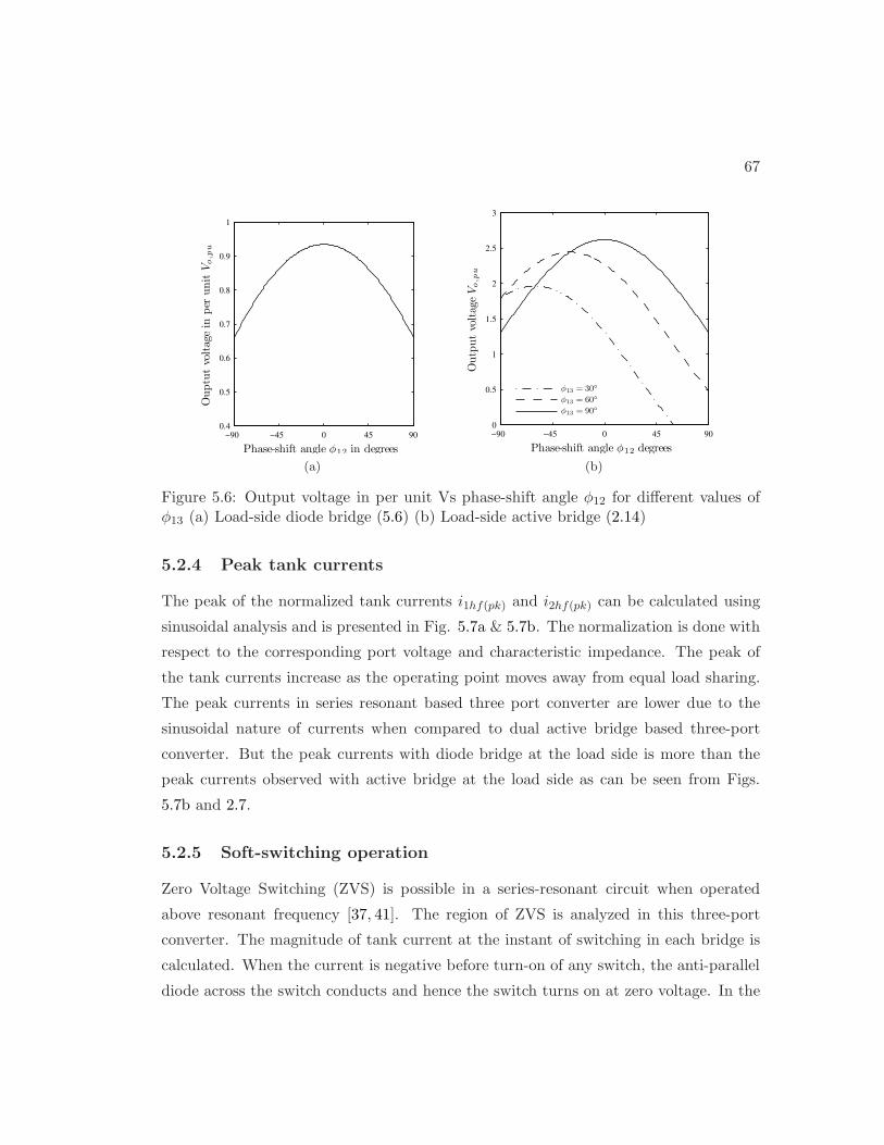
67
−90 −45 0 45 900.4
0.5
0.6
0.7
0.8
0.9
1
Phase-shift angle φ12 in degrees
Ouptu
tvo
ltag
ein
per
unit
Vo
,pu
(a)
−90 −45 0 45 900
0.5
1
1.5
2
2.5
3
Phase-shift angle φ12 degrees
Outp
ut
voltag
eV
o,p
u
φ13 = 30
φ13 = 60
φ13 = 90
(b)
Figure 5.6: Output voltage in per unit Vs phase-shift angle φ12 for different values ofφ13 (a) Load-side diode bridge (5.6) (b) Load-side active bridge (2.14)
5.2.4 Peak tank currents
The peak of the normalized tank currents i1hf(pk) and i2hf(pk) can be calculated using
sinusoidal analysis and is presented in Fig. 5.7a & 5.7b. The normalization is done with
respect to the corresponding port voltage and characteristic impedance. The peak of
the tank currents increase as the operating point moves away from equal load sharing.
The peak currents in series resonant based three port converter are lower due to the
sinusoidal nature of currents when compared to dual active bridge based three-port
converter. But the peak currents with diode bridge at the load side is more than the
peak currents observed with active bridge at the load side as can be seen from Figs.
5.7b and 2.7.
5.2.5 Soft-switching operation
Zero Voltage Switching (ZVS) is possible in a series-resonant circuit when operated
above resonant frequency [37, 41]. The region of ZVS is analyzed in this three-port
converter. The magnitude of tank current at the instant of switching in each bridge is
calculated. When the current is negative before turn-on of any switch, the anti-parallel
diode across the switch conducts and hence the switch turns on at zero voltage. In the
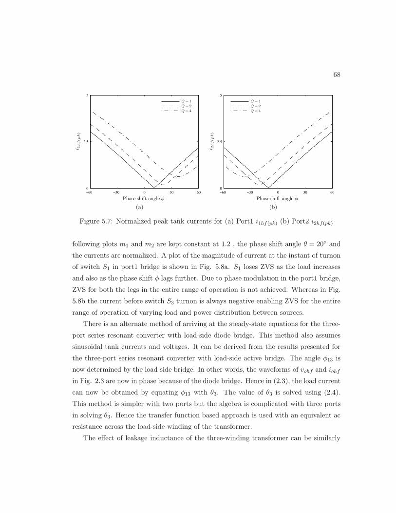
68
−60 −30 0 30 600
2.5
5
Phase-shift angle φ
i 1h
f(p
k)
Q = 1
Q = 2Q = 4
(a)
−60 −30 0 30 600
2.5
5
Phase-shift angle φ
i 2h
f(p
k)
Q = 1
Q = 2Q = 4
(b)
Figure 5.7: Normalized peak tank currents for (a) Port1 i1hf(pk) (b) Port2 i2hf(pk)
following plots m1 and m2 are kept constant at 1.2 , the phase shift angle θ = 20 and
the currents are normalized. A plot of the magnitude of current at the instant of turnon
of switch S1 in port1 bridge is shown in Fig. 5.8a. S1 loses ZVS as the load increases
and also as the phase shift φ lags further. Due to phase modulation in the port1 bridge,
ZVS for both the legs in the entire range of operation is not achieved. Whereas in Fig.
5.8b the current before switch S3 turnon is always negative enabling ZVS for the entire
range of operation of varying load and power distribution between sources.
There is an alternate method of arriving at the steady-state equations for the three-
port series resonant converter with load-side diode bridge. This method also assumes
sinusoidal tank currents and voltages. It can be derived from the results presented for
the three-port series resonant converter with load-side active bridge. The angle φ13 is
now determined by the load side bridge. In other words, the waveforms of vohf and iohf
in Fig. 2.3 are now in phase because of the diode bridge. Hence in (2.3), the load current
can now be obtained by equating φ13 with θ3. The value of θ3 is solved using (2.4).
This method is simpler with two ports but the algebra is complicated with three ports
in solving θ3. Hence the transfer function based approach is used with an equivalent ac
resistance across the load-side winding of the transformer.
The effect of leakage inductance of the three-winding transformer can be similarly
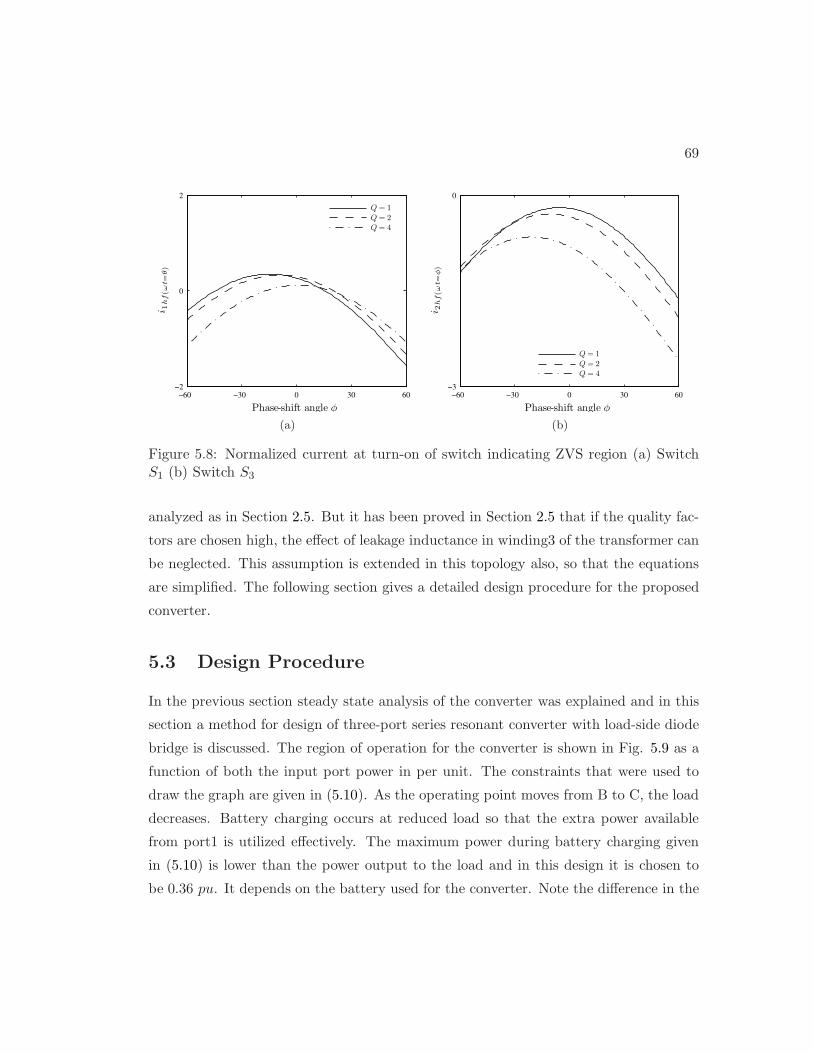
69
−60 −30 0 30 60−2
0
2
Phase-shift angle φ
i 1h
f(ω
t=θ)
Q = 1
Q = 2Q = 4
(a)
−60 −30 0 30 60−3
0
Phase-shift angle φ
i 2h
f(ω
t=φ)
Q = 1Q = 2Q = 4
(b)
Figure 5.8: Normalized current at turn-on of switch indicating ZVS region (a) SwitchS1 (b) Switch S3
analyzed as in Section 2.5. But it has been proved in Section 2.5 that if the quality fac-
tors are chosen high, the effect of leakage inductance in winding3 of the transformer can
be neglected. This assumption is extended in this topology also, so that the equations
are simplified. The following section gives a detailed design procedure for the proposed
converter.
5.3 Design Procedure
In the previous section steady state analysis of the converter was explained and in this
section a method for design of three-port series resonant converter with load-side diode
bridge is discussed. The region of operation for the converter is shown in Fig. 5.9 as a
function of both the input port power in per unit. The constraints that were used to
draw the graph are given in (5.10). As the operating point moves from B to C, the load
decreases. Battery charging occurs at reduced load so that the extra power available
from port1 is utilized effectively. The maximum power during battery charging given
in (5.10) is lower than the power output to the load and in this design it is chosen to
be 0.36 pu. It depends on the battery used for the converter. Note the difference in the

70
E(0.36,−0.36) D(1,−0.36)
A(0, 1)P2,pu
P1,pu
B(0.5, 0.5)
O(0, 0)
C(1, 0)
Figure 5.9: Operating region of series resonant three-port converter with load-side diodebridge
operating regions of Fig. 4.1 and Fig. 5.9.
0 ≤ P1,pu + P2,pu ≤ 1
−0.36 ≤ P2,pu ≤ 1
0 ≤ P1,pu ≤ 1 (5.10)
The parameters m1 and m2 are selected such that the converter is able to operate
at points A and D shown in Fig. 5.9 for a chosen value of quality factor. In other words
there must exist finite values of θ and φ such that the output voltage is maintained
at 1 pu and satisfy points A and D in the graph. This is found out by numerically
evaluating (5.6), (5.7) and (5.8). From known values of input voltages V1 and V2 the
turns ratio can be selected using (5.5). Given the switching frequency Fs and the
ratio of switching frequency to resonant frequency which in this case chosen as 1.1, the
series resonant parameters are calculated using (5.2). As the design satisfies at extreme
operating points A and D, it is found that the converter can operate at any point inside
and the boundary of the region in Fig. 5.9 by varying θ and φ. As the operating point
moves from A to D along the boundary, the port 2 side bridge does ZVS as explained
in Section 5.2.
Using the design procedure mentioned above, the values of the converter parameters
are chosen with the calculation done in Mathematica c©. The results of the design of a
500W converter using this procedure is summarized in Table 5.1. The values of m1 and
m2 are found to be 1.2 and 1.4 respectively.

71
Table 5.1: Designed component values of a Po = 500W output three-port series resonantconverter with load-side diode bridge
Parameter Value Units
L1 15.0 µH
L2 7.1 µH
C1 0.22 µF
C2 0.47 µF
Co 220 µF
V1 50 V
V2 36 V
n1 : n3 0.208:1
n2 : n3 0.125:1
5.4 Simulation results
5.4.1 Simulation method
Simulation of the three-port series resonant converter is performed in Saber c© with input
voltages chosen as V1 = 50V and V2 = 36V which is equivalent to three 12V batteries
connected in series. The output voltage Vo is kept around 200V by adjusting the phase
shifts. Simulation is performed in open loop. The converter switches at Fs = 100kHz
which is 1.1 times above the resonant frequency of both the resonant tanks.
Simulation is also performed in Matlab using an exact model of the converter (5.11-
5.15). Using the exact model, the series resonant tank parameters such as the peak
tank currents and voltages which are needed to design the tank inductor and capacitor
are calculated. Other parameters such as the transformer VA rating, switch currents,
input and output filter design are also estimated in simulation. The analysis presented
in the previous section uses sinusoidal approximation. A comparison of results obtained
through sinusoidal approximation and the exact model are also presented.
L1 iL1 =V1
2
(
sgn(sin (ωst − θ) + sgn(sin (ωst + θ))))
− vC1
− n1
n3vo sgn
(
n1
n3iL1 +
n2
n3iL2
)
(5.11)
C1vC1 = iL1 (5.12)
L2 iL2 = V2 sgn(sin (ωst + φ)) − vC2
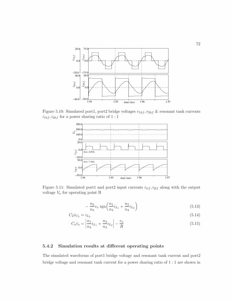
72
−50.0
0.0
50.0
time (ms)1.94 1.96 1.971.95−40.0
0.0
40.0−75.0
0.0
75.0
−20.0
0.0
20.0
v2h
f
i 2h
f
v1h
f
i 1h
f
Figure 5.10: Simulated port1, port2 bridge voltages v1hf , v2hf & resonant tank currentsi1hf , i2hf for a power sharing ratio of 1 : 1
−50.0
0.0
50.0
time (ms)1.951.94 1.96 1.97
−20.0
0.0
20.00.0
100.0
200.0
300.0
Ave: 4.05A
Ave: 7.34A
i 1lf
Vo
i 2lf
Figure 5.11: Simulated port1 and port2 input currents i1lf , i2lf along with the outputvoltage Vo for operating point B
− n2
n3vo sgn
(
n1
n3iL1 +
n2
n3iL2
)
(5.13)
C2vC2 = iL2 (5.14)
Covo =
∣
∣
∣
∣
n1
n3iL1 +
n2
n3iL2
∣
∣
∣
∣
− vo
R(5.15)
5.4.2 Simulation results at different operating points
The simulated waveforms of port1 bridge voltage and resonant tank current and port2
bridge voltage and resonant tank current for a power sharing ratio of 1 : 1 are shown in
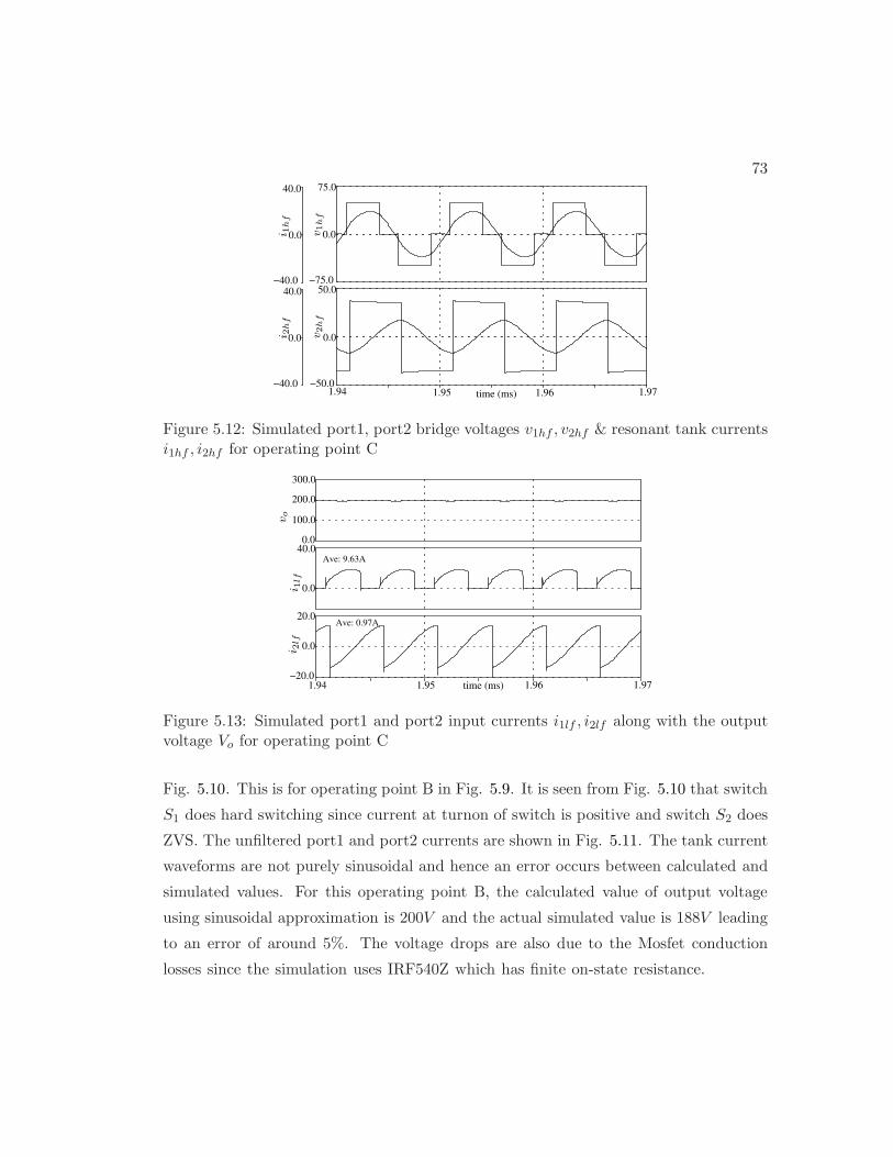
73
−50.0
0.0
50.0
time (ms)1.95 1.971.961.94−40.0
0.0
40.0−75.0
0.0
75.0
−40.0
0.0
40.0
i 1h
f
v1h
fv2h
f
i 2h
f
Figure 5.12: Simulated port1, port2 bridge voltages v1hf , v2hf & resonant tank currentsi1hf , i2hf for operating point C
−20.0
0.0
20.0
time (ms)1.951.94 1.96 1.97
0.0
40.00.0
100.0
200.0
300.0
Ave: 0.97A
Ave: 9.63A
i 2lf
i 1lf
vo
Figure 5.13: Simulated port1 and port2 input currents i1lf , i2lf along with the outputvoltage Vo for operating point C
Fig. 5.10. This is for operating point B in Fig. 5.9. It is seen from Fig. 5.10 that switch
S1 does hard switching since current at turnon of switch is positive and switch S2 does
ZVS. The unfiltered port1 and port2 currents are shown in Fig. 5.11. The tank current
waveforms are not purely sinusoidal and hence an error occurs between calculated and
simulated values. For this operating point B, the calculated value of output voltage
using sinusoidal approximation is 200V and the actual simulated value is 188V leading
to an error of around 5%. The voltage drops are also due to the Mosfet conduction
losses since the simulation uses IRF540Z which has finite on-state resistance.
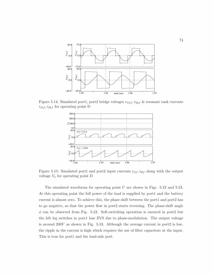
74
−50.0
0.0
50.0
time (ms)1.94 1.971.961.95−40.0
0.0
40.0−75.0
0.0
75.0
−40.0
0.0
40.0
v1h
f
i 2h
fi 1
hf
v2h
f
Figure 5.14: Simulated port1, port2 bridge voltages v1hf , v2hf & resonant tank currentsi1hf , i2hf for operating point D
−40.0
0.0
40.0
time (ms)1.951.94 1.96 1.97
−40.0
0.0
40.00.0
100.0
200.0
300.0
Ave: −3.86A
Ave: 9.31A
i 1lf
i 2lf
vo
Figure 5.15: Simulated port1 and port2 input currents i1lf , i2lf along with the outputvoltage Vo for operating point D
The simulated waveforms for operating point C are shown in Figs. 5.12 and 5.13.
At this operating point the full power of the load is supplied by port1 and the battery
current is almost zero. To achieve this, the phase shift between the port1 and port2 has
to go negative, so that the power flow in port2 starts reversing. The phase-shift angle
φ can be observed from Fig. 5.12. Soft-switching operation is ensured in port2 but
the left leg switches in port1 lose ZVS due to phase-modulation. The output voltage
is around 200V as shown in Fig. 5.13. Although the average current in port2 is low,
the ripple in the current is high which requires the use of filter capacitors at the input.
This is true for port1 and the load-side port.
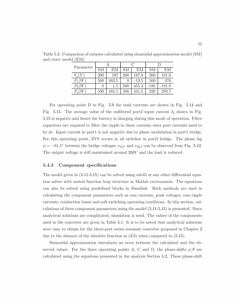
75
Table 5.2: Comparison of outputs calculated using sinusoidal approximation model (SM)and exact model (EM)
ParameterA C D
SM EM SM EM SM EM
Vo(V ) 200 197 200 187.9 200 191.6
P1(W ) 500 483.5 0 -13.5 500 476
P2(W ) 0 1.5 500 455.4 -180 -181.8
Po(W ) 500 485.1 500 441.5 320 293.7
For operating point D in Fig. 5.9 the tank currents are shown in Fig. 5.14 and
Fig. 5.15. The average value of the unfiltered port2 input current I2 shown in Fig.
5.15 is negative and hence the battery is charging during this mode of operation. Filter
capacitors are required to filter the ripple in these currents since port currents need to
be dc. Input current in port1 is not negative due to phase modulation in port1 bridge.
For this operating point, ZVS occurs in all switches in port2 bridge. The phase lag
φ = −61.5 between the bridge voltages v1hf and v2hf can be observed from Fig. 5.12.
The output voltage is still maintained around 200V and the load is reduced.
5.4.3 Component specifications
The model given in (5.11-5.15) can be solved using ode45 or any other differential equa-
tion solver with nested function loop structure in Matlab environment. The equations
can also be solved using predefined blocks in Simulink. Both methods are used in
calculating the component parameters such as rms currents, peak voltages, rms ripple
currents, conduction losses and soft-switching operating conditions. In this section, cal-
culations of these component parameters using the model (5.11-5.15) is presented. Since
analytical solutions are complicated, simulation is used. The values of the components
used in the converter are given in Table 5.1. It is to be noted that analytical solutions
were easy to obtain for the three-port series resonant converter proposed in Chapter 2
due to the absence of the absolute function in (3.5) when compared to (5.15).
Sinusoidal approximation introduces an error between the calculated and the ob-
served values. For the three operating points A, C and D, the phase-shifts φ, θ are
calculated using the equations presented in the analysis Section 5.2. These phase-shift
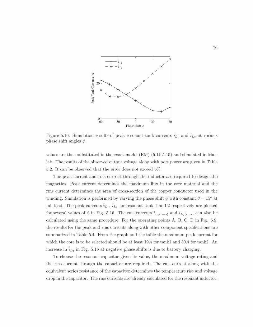
76
−60 −30 0 30 600
20
Phase-shift φ
Pea
k T
ank C
urr
ents
(A
)
iL1
iL2
Figure 5.16: Simulation results of peak resonant tank currents iL1 and iL2 at variousphase shift angles φ
values are then substituted in the exact model (EM) (5.11-5.15) and simulated in Mat-
lab. The results of the observed output voltage along with port power are given in Table
5.2. It can be observed that the error does not exceed 5%.
The peak current and rms current through the inductor are required to design the
magnetics. Peak current determines the maximum flux in the core material and the
rms current determines the area of cross-section of the copper conductor used in the
winding. Simulation is performed by varying the phase shift φ with constant θ = 15o at
full load. The peak currents iL1 , iL2 for resonant tank 1 and 2 respectively are plotted
for several values of φ in Fig. 5.16. The rms currents iL1(rms) and iL2(rms) can also be
calculated using the same procedure. For the operating points A, B, C, D in Fig. 5.9,
the results for the peak and rms currents along with other component specifications are
summarized in Table 5.4. From the graph and the table the maximum peak current for
which the core is to be selected should be at least 19A for tank1 and 30A for tank2. An
increase in iL2 in Fig. 5.16 at negative phase shifts is due to battery charging.
To choose the resonant capacitor given its value, the maximum voltage rating and
the rms current through the capacitor are required. The rms current along with the
equivalent series resistance of the capacitor determines the temperature rise and voltage
drop in the capacitor. The rms currents are already calculated for the resonant inductor.
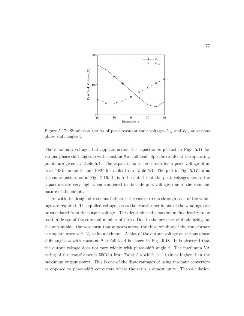
77
−60 −30 0 30 600
100
200
Phase-shift φ
Pea
k T
ank V
olt
ages
(V
)
vC1
vC2
Figure 5.17: Simulation results of peak resonant tank voltages vC1 and vC2 at variousphase shift angles φ
The maximum voltage that appears across the capacitor is plotted in Fig. 5.17 for
various phase shift angles φ with constant θ at full load. Specific results at the operating
points are given in Table 5.4. The capacitor is to be chosen for a peak voltage of at
least 143V for tank1 and 108V for tank2 from Table 5.4. The plot in Fig. 5.17 forms
the same pattern as in Fig. 5.16. It is to be noted that the peak voltages across the
capacitors are very high when compared to their dc port voltages due to the resonant
nature of the circuit.
As with the design of resonant inductor, the rms currents through each of the wind-
ings are required. The applied voltage across the transformer in one of the windings can
be calculated from the output voltage . This determines the maximum flux density to be
used in design of the core and number of turns. Due to the presence of diode bridge at
the output side, the waveform that appears across the third winding of the transformer
is a square wave with Vo as its maximum. A plot of the output voltage at various phase
shift angles φ with constant θ at full load is shown in Fig. 5.18. It is observed that
the output voltage does not vary widely with phase-shift angle φ. The maximum VA
rating of the transformer is 550V A from Table 5.4 which is 1.1 times higher than the
maximum output power. This is one of the disadvantages of using resonant converters
as opposed to phase-shift converters where the ratio is almost unity. The calculation
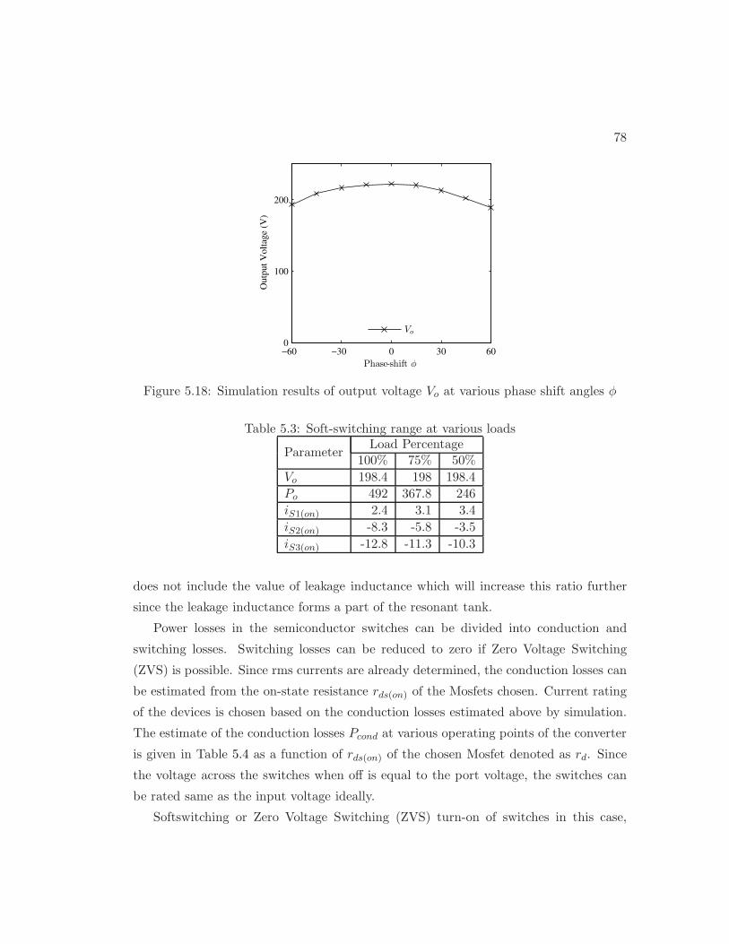
78
−60 −30 0 30 600
100
200
Phase-shift φ
Outp
ut
Volt
age
(V)
Vo
Figure 5.18: Simulation results of output voltage Vo at various phase shift angles φ
Table 5.3: Soft-switching range at various loads
ParameterLoad Percentage
100% 75% 50%
Vo 198.4 198 198.4
Po 492 367.8 246
iS1(on) 2.4 3.1 3.4
iS2(on) -8.3 -5.8 -3.5
iS3(on) -12.8 -11.3 -10.3
does not include the value of leakage inductance which will increase this ratio further
since the leakage inductance forms a part of the resonant tank.
Power losses in the semiconductor switches can be divided into conduction and
switching losses. Switching losses can be reduced to zero if Zero Voltage Switching
(ZVS) is possible. Since rms currents are already determined, the conduction losses can
be estimated from the on-state resistance rds(on) of the Mosfets chosen. Current rating
of the devices is chosen based on the conduction losses estimated above by simulation.
The estimate of the conduction losses Pcond at various operating points of the converter
is given in Table 5.4 as a function of rds(on) of the chosen Mosfet denoted as rd. Since
the voltage across the switches when off is equal to the port voltage, the switches can
be rated same as the input voltage ideally.
Softswitching or Zero Voltage Switching (ZVS) turn-on of switches in this case,
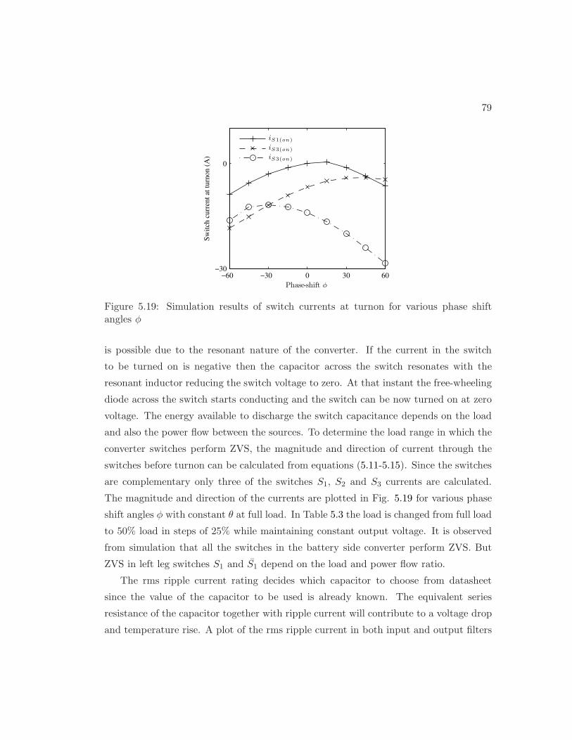
79
−60 −30 0 30 60−30
0
Phase-shift φ
Sw
itch
curr
ent
at t
urn
on (
A)
iS1(on)
iS3(on)
iS3(on)
Figure 5.19: Simulation results of switch currents at turnon for various phase shiftangles φ
is possible due to the resonant nature of the converter. If the current in the switch
to be turned on is negative then the capacitor across the switch resonates with the
resonant inductor reducing the switch voltage to zero. At that instant the free-wheeling
diode across the switch starts conducting and the switch can be now turned on at zero
voltage. The energy available to discharge the switch capacitance depends on the load
and also the power flow between the sources. To determine the load range in which the
converter switches perform ZVS, the magnitude and direction of current through the
switches before turnon can be calculated from equations (5.11-5.15). Since the switches
are complementary only three of the switches S1, S2 and S3 currents are calculated.
The magnitude and direction of the currents are plotted in Fig. 5.19 for various phase
shift angles φ with constant θ at full load. In Table 5.3 the load is changed from full load
to 50% load in steps of 25% while maintaining constant output voltage. It is observed
from simulation that all the switches in the battery side converter perform ZVS. But
ZVS in left leg switches S1 and S1 depend on the load and power flow ratio.
The rms ripple current rating decides which capacitor to choose from datasheet
since the value of the capacitor to be used is already known. The equivalent series
resistance of the capacitor together with ripple current will contribute to a voltage drop
and temperature rise. A plot of the rms ripple current in both input and output filters
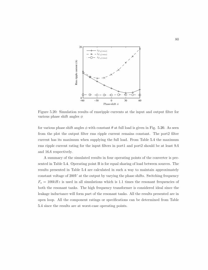
80
−60 −30 0 30 600
20
Phase-shift φ
Rm
s ri
pple
curr
ent
(A)
iC3(rms)
iC4(rms)
iCo(rms)
Figure 5.20: Simulation results of rmsripple currents at the input and output filter forvarious phase shift angles φ
for various phase shift angles φ with constant θ at full load is given in Fig. 5.20. As seen
from the plot the output filter rms ripple current remains constant. The port2 filter
current has its maximum when supplying the full load. From Table 5.4 the maximum
rms ripple current rating for the input filters in port1 and port2 should be at least 9A
and 16A respectively.
A summary of the simulated results in four operating points of the converter is pre-
sented in Table 5.4. Operating point B is for equal sharing of load between sources. The
results presented in Table 5.4 are calculated in such a way to maintain approximately
constant voltage of 200V at the output by varying the phase shifts. Switching frequency
Fs = 100kHz is used in all simulations which is 1.1 times the resonant frequencies of
both the resonant tanks. The high frequency transformer is considered ideal since the
leakage inductance will form part of the resonant tanks. All the results presented are in
open loop. All the component ratings or specifications can be determined from Table
5.4 since the results are at worst-case operating points.
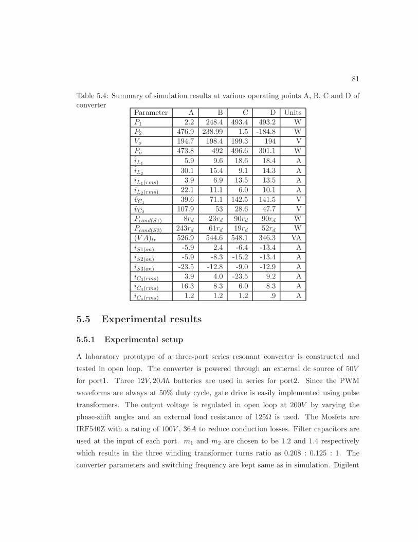
81
Table 5.4: Summary of simulation results at various operating points A, B, C and D ofconverter
Parameter A B C D Units
P1 2.2 248.4 493.4 493.2 W
P2 476.9 238.99 1.5 -184.8 W
Vo 194.7 198.4 199.3 194 V
Po 473.8 492 496.6 301.1 W
iL1 5.9 9.6 18.6 18.4 A
iL2 30.1 15.4 9.1 14.3 A
iL1(rms) 3.9 6.9 13.5 13.5 A
iL2(rms) 22.1 11.1 6.0 10.1 A
vC1 39.6 71.1 142.5 141.5 V
vC2 107.9 53 28.6 47.7 V
Pcond(S1) 8rd 23rd 90rd 90rd W
Pcond(S3) 243rd 61rd 19rd 52rd W
(V A)tr 526.9 544.6 548.1 346.3 VA
iS1(on) -5.9 2.4 -6.4 -13.4 A
iS2(on) -5.9 -8.3 -15.2 -13.4 A
iS3(on) -23.5 -12.8 -9.0 -12.9 A
iC3(rms) 3.9 4.0 -23.5 9.2 A
iC4(rms) 16.3 8.3 6.0 8.3 A
iCo(rms) 1.2 1.2 1.2 .9 A
5.5 Experimental results
5.5.1 Experimental setup
A laboratory prototype of a three-port series resonant converter is constructed and
tested in open loop. The converter is powered through an external dc source of 50V
for port1. Three 12V, 20Ah batteries are used in series for port2. Since the PWM
waveforms are always at 50% duty cycle, gate drive is easily implemented using pulse
transformers. The output voltage is regulated in open loop at 200V by varying the
phase-shift angles and an external load resistance of 125Ω is used. The Mosfets are
IRF540Z with a rating of 100V , 36A to reduce conduction losses. Filter capacitors are
used at the input of each port. m1 and m2 are chosen to be 1.2 and 1.4 respectively
which results in the three winding transformer turns ratio as 0.208 : 0.125 : 1. The
converter parameters and switching frequency are kept same as in simulation. Digilent

82
w/ load−side diode bridge
Three batteries (36V)
Load
FPGA for PWM
Three−port converter
Figure 5.21: Hardware setup for testing the series resonant three-port converter withload-side diode bridge
Basys c© FPGA board is used to program the phase shift angles and generate the PWM
pulses for both the bridges. The pulses for the Mosfets are generated using a double-
ramp carrier signal [40] and two control voltages for the two phase-shifts. It is to be
noted that the phase-shift modulation for port1 bridge uses center modulation, i.e., the
left and right legs get phase-shifted by the same angle from a center reference. The
hardware setup for testing is shown in Fig. 5.21
5.5.2 Prototype results
Experimental waveforms of port1 bridge voltage and resonant tank current and port2
bridge voltage and resonant tank current are shown in Fig. 5.22 and Fig. 5.23 re-
spectively for almost equal sharing of 350W load. The observed efficiency is 91%. All
switches in port2 bridge turnon at zero voltage as can be observed from Fig. 5.23 since
the tank current lags the applied port2 voltage. In port1 only the right leg having the
switch S3 performs ZVS. S1 loses ZVS since the current before turn-on is positive as
seen from Fig. 5.22. The winding3 voltage waveform is shown in Fig. 5.24 which is
a square wave voltage with a magnitude of 200V and the current through the diode
bridge is in phase with the voltage. Port1 dc voltage along with the port1 filtered input
current is shown in Fig. 5.25 to indicate equal sharing of load. The zero phase-shift
between the port1 and port2 bridge voltages can also be observed from Fig. 5.22 and
Fig. 5.23, since they are triggered at the same time in the oscilloscope.
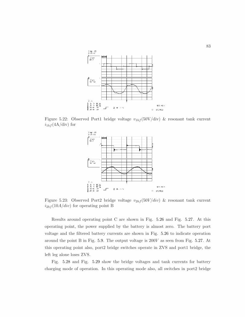
83
Figure 5.22: Observed Port1 bridge voltage v1hf (50V/div) & resonant tank currenti1hf (4A/div) for
Figure 5.23: Observed Port2 bridge voltage v2hf (50V/div) & resonant tank currenti2hf (10A/div) for operating point B
Results around operating point C are shown in Fig. 5.26 and Fig. 5.27. At this
operating point, the power supplied by the battery is almost zero. The battery port
voltage and the filtered battery currents are shown in Fig. 5.26 to indicate operation
around the point B in Fig. 5.9. The output voltage is 200V as seen from Fig. 5.27. At
this operating point also, port2 bridge switches operate in ZVS and port1 bridge, the
left leg alone loses ZVS.
Fig. 5.28 and Fig. 5.29 show the bridge voltages and tank currents for battery
charging mode of operation. In this operating mode also, all switches in port2 bridge
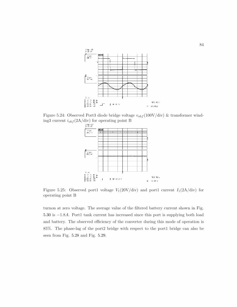
84
Figure 5.24: Observed Port3 diode bridge voltage vohf (100V/div) & transformer wind-ing3 current iohf (2A/div) for operating point B
Figure 5.25: Observed port1 voltage V1(20V/div) and port1 current I1(2A/div) foroperating point B
turnon at zero voltage. The average value of the filtered battery current shown in Fig.
5.30 is −1.8A. Port1 tank current has increased since this port is supplying both load
and battery. The observed efficiency of the converter during this mode of operation is
85%. The phase-lag of the port2 bridge with respect to the port1 bridge can also be
seen from Fig. 5.28 and Fig. 5.29.
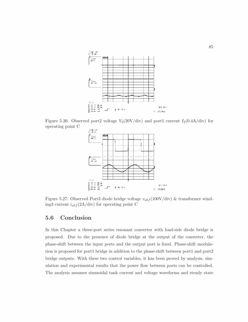
85
Figure 5.26: Observed port2 voltage V2(20V/div) and port1 current I2(0.4A/div) foroperating point C
Figure 5.27: Observed Port3 diode bridge voltage vohf (100V/div) & transformer wind-ing3 current iohf (2A/div) for operating point C
5.6 Conclusion
In this Chapter a three-port series resonant converter with load-side diode bridge is
proposed. Due to the presence of diode bridge at the output of the converter, the
phase-shift between the input ports and the output port is fixed. Phase-shift modula-
tion is proposed for port1 bridge in addition to the phase-shift between port1 and port2
bridge outputs. With these two control variables, it has been proved by analysis, sim-
ulation and experimental results that the power flow between ports can be controlled.
The analysis assumes sinusoidal tank current and voltage waveforms and steady state
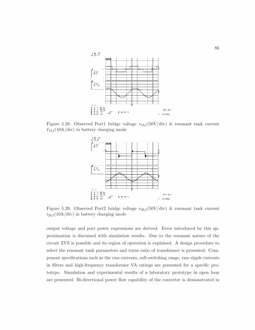
86
Figure 5.28: Observed Port1 bridge voltage v1hf (50V/div) & resonant tank currentI1hf (10A/div) in battery charging mode
Figure 5.29: Observed Port2 bridge voltage v2hf (50V/div) & resonant tank currenti2hf (10A/div) in battery charging mode
output voltage and port power expressions are derived. Error introduced by this ap-
proximation is discussed with simulation results. Due to the resonant nature of the
circuit ZVS is possible and its region of operation is explained. A design procedure to
select the resonant tank parameters and turns ratio of transformer is presented. Com-
ponent specifications such as the rms currents, soft-switching range, rms ripple currents
in filters and high-frequency transformer VA ratings are presented for a specific pro-
totype. Simulation and experimental results of a laboratory prototype in open loop
are presented. Bi-directional power flow capability of the converter is demonstrated in

87
Figure 5.30: Observed battery voltage V2(20V/div) & charging current I2(1A/div) inbattery charging mode
hardware using battery as one of the sources.

Chapter 6
Current-fed Three-port
Converter
In the previous Chapters, three-port dc-dc converters using the principle of series res-
onance was explained. In this Chapter, another three-port converter topology is intro-
duced which uses current-fed input ports as opposed to voltage-fed input ports. Current-
fed input ports ensure dc currents at the input thereby eliminating the need of large
filter capacitors. The proposed three-port current-fed converter is presented followed
by detailed steady-state and dynamic analysis. Design, simulation and experimental
results follow the analysis.
6.1 Introduction
Current-fed topologies have the distinct advantage of dc currents at all ports, over
voltage-fed topologies. This is advantageous if the source connected to the port is a
battery or fuel-cell. It eliminates the need of large filter capacitors at the input and
thereby increasing the overall reliability of the converter. A two-port voltage-fed bi-
directional dc-dc converter was proposed in [6] for high power applications. It uses
two active bridges at the two ports with the transformer and the inductor at the high
frequency side. The power flow is controlled by the phase-shift between active bridges
along with or without PWM and frequency control. Such a Dual Active Bridge (DAB)
converter [6] is shown in Fig. 6.1. The topology is voltage-fed and hence the converter
88
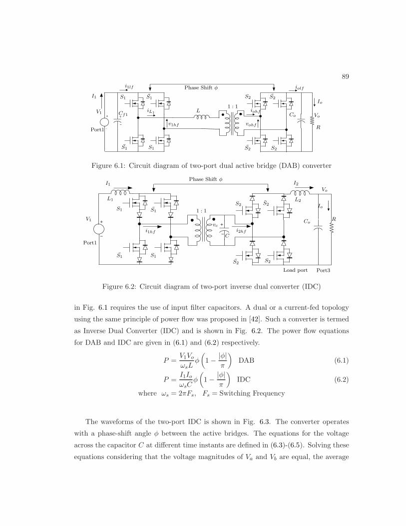
89
−
+
−
+
LCf1
iL1
S2 S2
vohf
Co
S1 S1
Phase Shift φ
Io
R
i1lf
Vo
iolf
S2S2S1S1
iohf
I1
1 : 1
v1hf
V1
Port1
Figure 6.1: Circuit diagram of two-port dual active bridge (DAB) converter
+
−
+
−
1 : 1
Vo
Io
R
Load port Port3
S2 S2
S2
Phase Shift φ
Co
S1 S1
S1 S1
I2I1
L1 L2
i1hfC
i2hf
vc
V1
Port1
S2
Figure 6.2: Circuit diagram of two-port inverse dual converter (IDC)
in Fig. 6.1 requires the use of input filter capacitors. A dual or a current-fed topology
using the same principle of power flow was proposed in [42]. Such a converter is termed
as Inverse Dual Converter (IDC) and is shown in Fig. 6.2. The power flow equations
for DAB and IDC are given in (6.1) and (6.2) respectively.
P =V1Vo
ωsLφ
(
1 − |φ|π
)
DAB (6.1)
P =I1Io
ωsCφ
(
1 − |φ|π
)
IDC (6.2)
where ωs = 2πFs, Fs = Switching Frequency
The waveforms of the two-port IDC is shown in Fig. 6.3. The converter operates
with a phase-shift angle φ between the active bridges. The equations for the voltage
across the capacitor C at different time instants are defined in (6.3)-(6.5). Solving these
equations considering that the voltage magnitudes of Va and Vb are equal, the average
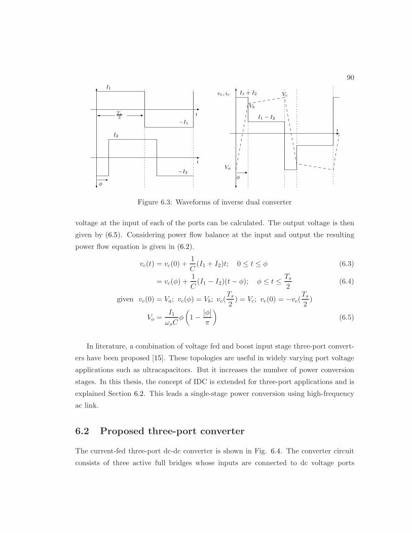
90
t
t
t
vc, ic
I1
−I1
I2
−I2
I1 + I2
I1 − I2
φ
Ts
2
φ
Va
Vb
Vc
Figure 6.3: Waveforms of inverse dual converter
voltage at the input of each of the ports can be calculated. The output voltage is then
given by (6.5). Considering power flow balance at the input and output the resulting
power flow equation is given in (6.2).
vc(t) = vc(0) +1
C(I1 + I2)t; 0 ≤ t ≤ φ (6.3)
= vc(φ) +1
C(I1 − I2)(t − φ); φ ≤ t ≤ Ts
2(6.4)
given vc(0) = Va; vc(φ) = Vb; vc(Ts
2) = Vc; vc(0) = −vc(
Ts
2)
Vo =I1
ωsCφ
(
1 − |φ|π
)
(6.5)
In literature, a combination of voltage fed and boost input stage three-port convert-
ers have been proposed [15]. These topologies are useful in widely varying port voltage
applications such as ultracapacitors. But it increases the number of power conversion
stages. In this thesis, the concept of IDC is extended for three-port applications and is
explained Section 6.2. This leads a single-stage power conversion using high-frequency
ac link.
6.2 Proposed three-port converter
The current-fed three-port dc-dc converter is shown in Fig. 6.4. The converter circuit
consists of three active full bridges whose inputs are connected to dc voltage ports
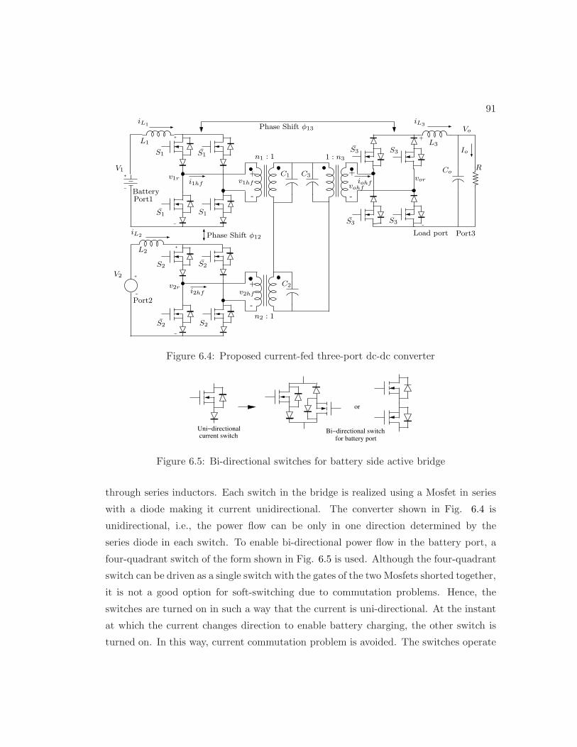
91
−
+
−
−
+
−
+
+
vor
iL1
L1
S1 S1
S1 S1
V1
V2
iL2
L2
S2
i2hf
S2 S2
n2 : 1
C2
S2
Phase Shift φ12
n1 : 1
Phase Shift φ13
C1 C3
1 : n3
S3 S3
iL3
Vo
Io
L3
CoR
S3S3
Load port Port3
iohf
BatteryPort1
Port2
+v1hf
+
-
v2hf
+
--
vohfi1hf
v1r
v2r
+
-
Figure 6.4: Proposed current-fed three-port dc-dc converter
or
current switchUni−directional Bi−directional switch
for battery port
Figure 6.5: Bi-directional switches for battery side active bridge
through series inductors. Each switch in the bridge is realized using a Mosfet in series
with a diode making it current unidirectional. The converter shown in Fig. 6.4 is
unidirectional, i.e., the power flow can be only in one direction determined by the
series diode in each switch. To enable bi-directional power flow in the battery port, a
four-quadrant switch of the form shown in Fig. 6.5 is used. Although the four-quadrant
switch can be driven as a single switch with the gates of the two Mosfets shorted together,
it is not a good option for soft-switching due to commutation problems. Hence, the
switches are turned on in such a way that the current is uni-directional. At the instant
at which the current changes direction to enable battery charging, the other switch is
turned on. In this way, current commutation problem is avoided. The switches operate

92
at 50% duty cycle with an overlap time between transitions.
The outputs of the bridges are connected to three separate transformers whose sec-
ondary are configured in delta, with high frequency capacitors in parallel to each trans-
former secondary. In voltage-fed converters such as the ones shown in Fig. 1.4 and Fig.
2.2, the three-winding transformer naturally sums the currents through it to zero or in
other words, if the load is not regenerative, the current through the winding3 of the
transformer is the sum of the currents in the other two windings. Since the current-fed
topology is a dual of the voltage-fed topology, the voltages are summed up to zero by
the delta connection of the secondaries of the three transformers. In other words, if
the load is not regenerative, the voltage that appears across the load is the sum of the
voltages across the other two transformer secondaries. The input port currents are dc
due to the presence of inductor at the input side as shown in Fig. 6.4.
The capacitors C1, C2 and C3 are high frequency capacitors of very low value <
0.1µF . The dc side inductors L1, L2 and L3 are designed to have high values > 2mH
so that the port currents are dc with low ripple. Also, the resonant time period between
the dc side inductors and the high frequency capacitors is very high when compared
to the switching time period such that the charging of the capacitors is linear. The
converter switches operate at constant switching frequency Fs. The active bridges are
phase-shifted by the angles φ13 and φ12. The following section discusses the steady-state
analysis of the current-fed three-port converter.
6.3 Steady-state analysis
The square wave outputs and the corresponding phase-shifts are shown in Fig. 6.6a.
The phase-shifts φ13 and φ12 are considered positive if iohf lags i1hf and i2hf lags i1hf
respectively. I1, I2 and I3 are the magnitudes of the square waves. The waveforms of
the capacitor voltages across each transformer primary are shown in Fig. 6.6b. In the
series resonant circuit discussed in the previous chapters, sinusoidal approximation was
possible due to the filtering action of the resonant circuit. In this current-fed converter,
such an approximation is not possible, due to the high third and fifth harmonic com-
ponent in the voltage waveforms as seen from Fig. 6.6b. Hence a different approach in
deriving the steady-state equations is adopted. This approach is similar to the two-port
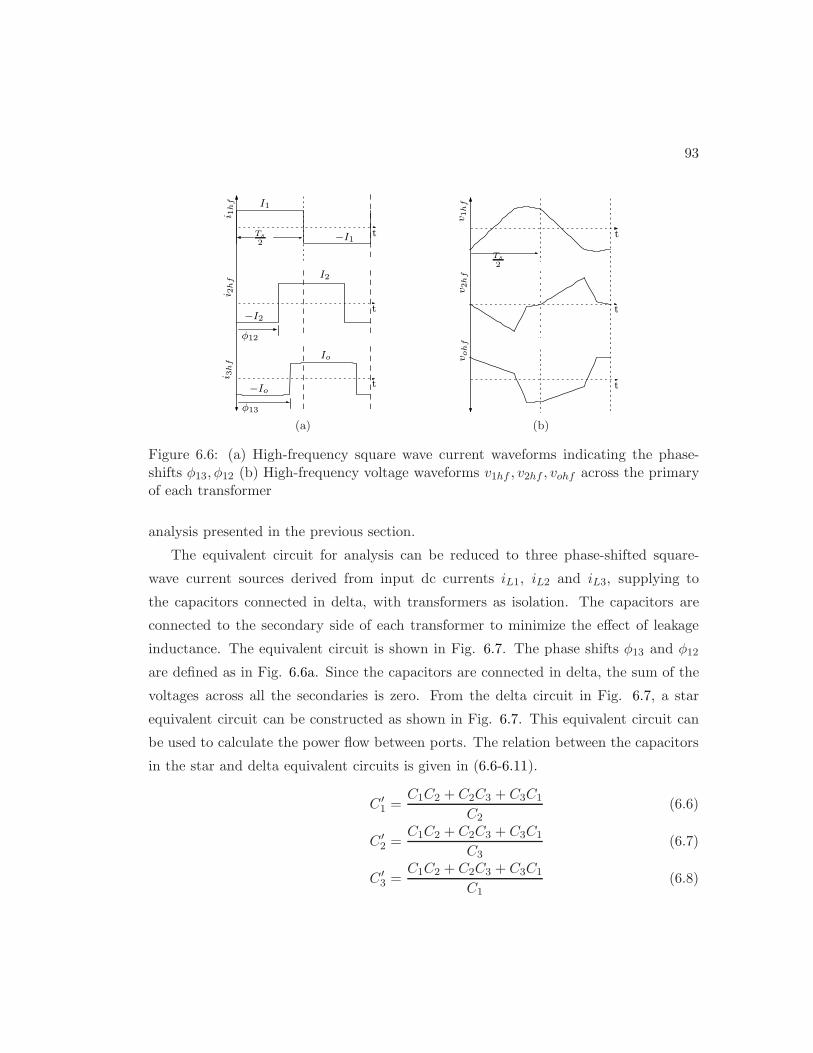
93
Ts
2
φ12
φ13
i 3h
fi 2
hf
i 1h
f I1
−I1
I2
−I2
Io
−Io
t
t
t
(a)
Ts
2
v2h
fv1h
fv
oh
f
t
t
t
(b)
Figure 6.6: (a) High-frequency square wave current waveforms indicating the phase-shifts φ13, φ12 (b) High-frequency voltage waveforms v1hf , v2hf , vohf across the primaryof each transformer
analysis presented in the previous section.
The equivalent circuit for analysis can be reduced to three phase-shifted square-
wave current sources derived from input dc currents iL1, iL2 and iL3, supplying to
the capacitors connected in delta, with transformers as isolation. The capacitors are
connected to the secondary side of each transformer to minimize the effect of leakage
inductance. The equivalent circuit is shown in Fig. 6.7. The phase shifts φ13 and φ12
are defined as in Fig. 6.6a. Since the capacitors are connected in delta, the sum of the
voltages across all the secondaries is zero. From the delta circuit in Fig. 6.7, a star
equivalent circuit can be constructed as shown in Fig. 6.7. This equivalent circuit can
be used to calculate the power flow between ports. The relation between the capacitors
in the star and delta equivalent circuits is given in (6.6-6.11).
C ′1 =
C1C2 + C2C3 + C3C1
C2(6.6)
C ′2 =
C1C2 + C2C3 + C3C1
C3(6.7)
C ′3 =
C1C2 + C2C3 + C3C1
C1(6.8)
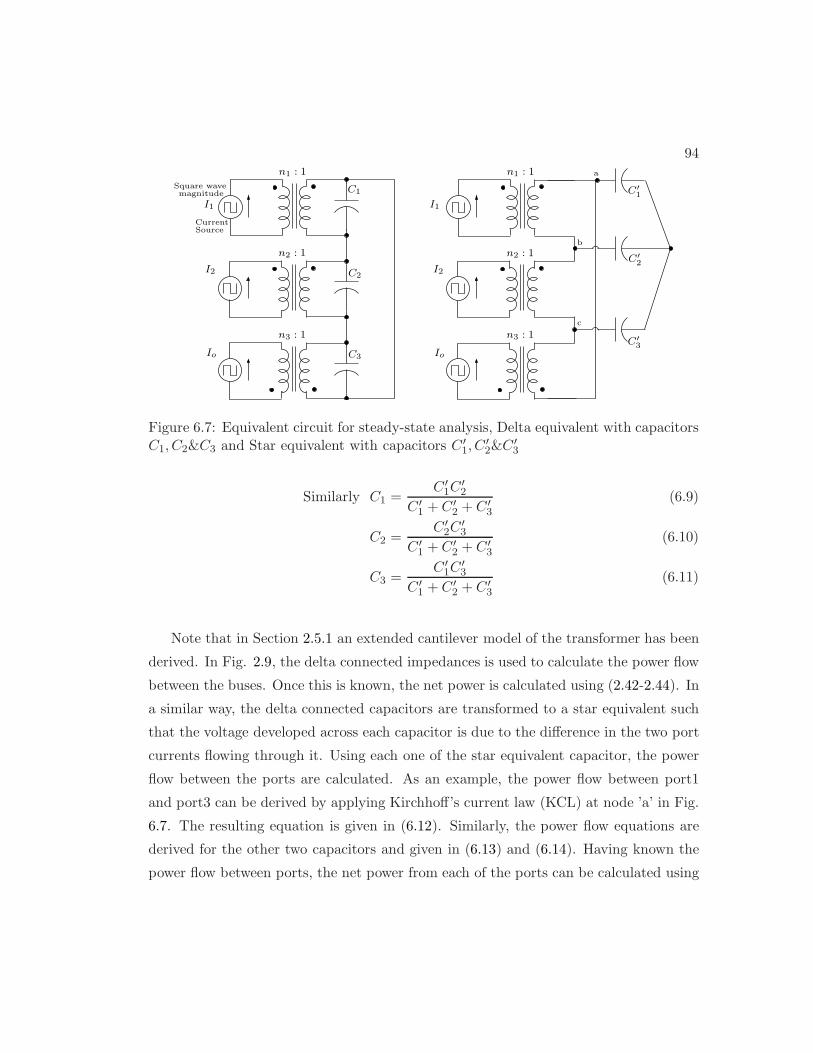
94
magnitude
n2 : 1
n1 : 1
n3 : 1
I1
I2
Io
C′
2
C′
1
C′
3
a
b
c
n2 : 1
n1 : 1
n3 : 1
C2
C3
C1
I2
Io
CurrentSource
I1
Square wave
Figure 6.7: Equivalent circuit for steady-state analysis, Delta equivalent with capacitorsC1, C2&C3 and Star equivalent with capacitors C ′
1, C′2&C ′
3
Similarly C1 =C ′
1C′2
C ′1 + C ′
2 + C ′3
(6.9)
C2 =C ′
2C′3
C ′1 + C ′
2 + C ′3
(6.10)
C3 =C ′
1C′3
C ′1 + C ′
2 + C ′3
(6.11)
Note that in Section 2.5.1 an extended cantilever model of the transformer has been
derived. In Fig. 2.9, the delta connected impedances is used to calculate the power flow
between the buses. Once this is known, the net power is calculated using (2.42-2.44). In
a similar way, the delta connected capacitors are transformed to a star equivalent such
that the voltage developed across each capacitor is due to the difference in the two port
currents flowing through it. Using each one of the star equivalent capacitor, the power
flow between the ports are calculated. As an example, the power flow between port1
and port3 can be derived by applying Kirchhoff’s current law (KCL) at node ’a’ in Fig.
6.7. The resulting equation is given in (6.12). Similarly, the power flow equations are
derived for the other two capacitors and given in (6.13) and (6.14). Having known the
power flow between ports, the net power from each of the ports can be calculated using

95
(6.15-6.17).
P13 =n1n3I1Io
ωsC ′1
φ13
(
1 − |φ13|π
)
(6.12)
P21 =n1n2I2I1
ωsC ′2
φ21
(
1 − |φ21|π
)
= −P12 (6.13)
P32 =n2n3I2Io
ωsC ′3
φ32
(
1 − |φ32|π
)
= −P23 (6.14)
P1 = P13 + P12 (6.15)
P2 = P23 − P12 (6.16)
Po = P23 + P13 (6.17)
Also, φ12 = −φ21; φ23 = −φ32
Under dc steady state, since the average of the voltage across the series inductor is
zero, the average voltage that appears at the input of the active bridges can be equated
to the port voltage as shown in (6.18). From (6.15-6.17) the power drawn from the
input ports and the power delivered to the load can be calculated. The load voltage is
given by (6.19) and the load power by (6.21).
V1 = v1r; V2 = v2r; Vo = vor; (6.18)
Vo =n1n3I1
ωsC ′1
φ13
(
1 − |φ13|π
)
+n2n3I2
ωsC ′3
φ23
(
1 − |φ23|π
)
(6.19)
Po = VoIo =V 2
o
R(6.20)
Po =n1n3I1Io
ωsC ′1
φ13
(
1 − |φ13|π
)
+n2n3I2Io
ωsC ′3
φ23
(
1 − |φ23|π
)
(6.21)
In the output voltage equation (6.19), the values of the port currents I1 and I2 are
unknown. Since Vo = IoR, the input port currents in terms of the output voltage Vo
can be derived from the port power equations and they are given in (6.22) and (6.23).
Substituting these values in (6.19), the final equation for the output voltage Vo is given
by (6.24).
I1 =−V2 + n2n3Vo
ωsRC′
3φ23
(
1 − |φ23|π
)
n1n2ωsC′
2φ12
(
1 − |φ12|π
) (6.22)

96
Table 6.1: Current-fed three-port converter specifications
Specification Value
Port1 voltage V1 50V
Port2 voltage V2 36 − 40V
Output power Po 0.5kW
Output voltage Vo 200V
I2 =V1 − n1n3Vo
ωsRC′
1φ13
(
1 − |φ13|π
)
n1n2ωsC′
2φ12
(
1 − |φ12|π
) (6.23)
Vo =C ′
2/n1n2
φ12
(
1 − |φ12|π
)
[
V1
C ′3/n2n3
φ23
(
1 − |φ23|π
)
− V2
C ′1/n1n3
φ13
(
1 − |φ13|π
)]
(6.24)
The load voltage Vo (6.24) is independent of the load resistance R, and hence the-
oretically the output voltage remains constant for load variations. This is one of the
advantages of this converter. In the practical circuit, the parasitic resistances and the
mosfet on-state resistances rds(on) will contribute to a drop in voltage as load increases.
The final port1 and port2 power equations are given by (6.25) and (6.26) respectively.
P1 =n1n3I1Io
ωsC ′1
φ13
(
1 − |φ13|π
)
+n1n2I1I2
ωsC ′2
φ12
(
1 − |φ12|π
)
(6.25)
P2 =n2n3I2Io
ωsC ′3
φ23
(
1 − |φ23|π
)
− n1n2I1I2
ωsC ′2
φ12
(
1 − |φ12|π
)
(6.26)
The design requirements for the current-fed three-port converter are the same as the
series resonant three-port converter explained in Chapter 4. The limit equations for the
port power and output power are repeated here (6.27-6.28). The converter specifications
are given in Table 6.1. The base power and the base voltage are chosen as the required
output power and the required output voltage. Hence the converter needs to maintain
a constant Vo,pu = 1.0 under various power sharing ratios and load power. Using the
steady-state equations of output voltage (6.24) and port power (6.25-6.26) the converter
parameters are designed and presented in Table 6.2. The source-side inductances L1,
L2 are large enough such that the port currents can be assumed dc and for steady-state

97
Table 6.2: Current-fed three-port converter parameters
Converter Parameter Value
Port1 Capacitor C1 15.0nF
Port2 Capacitor C2 3.3nF
Port3 Capacitor C2 6.2nF
Turns ratio n1 0.33
Turns ratio n2 0.42
Turns ratio n3 1
analysis the average voltages across these inductors are zero.
0 ≤ P1,pu ≤ 1 (6.27)
−0.5 ≤ P2,pu ≤ 1 (6.28)
Since P1,pu + P2,pu = Po,pu
−0.5 ≤ Po,pu ≤ 1 (6.29)
A plot of the output voltage in per unit as a function of phase-shift angle φ12 at
constant φ13 is shown in Fig. 6.8a. Similarly the output voltage as a function of phase-
shift angle φ13 is plotted in Fig. 6.8b. The requirement for the converter is to maintain
a constant output voltage. It can be observed that to maintain an output voltage of
1pu, the value of phase-shift φ13 should be higher than 90o for values of φ12 > 40o.
At low values of φ13, the output voltage can go negative unless the phase-shift φ12 is
reduced correspondingly.
The output voltage can theoretically reach infinity when phase shift φ12 tends toward
zero, but parasitic resistances limit its magnitude. Hence in the plots, the value of φ12 is
limited to 40o. The turns ratio of the three high frequency transformers can also be used
to vary the voltage step-up ratios. Note that the ports are still voltage ports as used in
the three-port series resonant converter but they are converted to current ports through
the use of series inductors. Hence the voltage plots with respect to the phase-shifts are
very different from what has been presented in the three-port series resonant converter.
Several pairs of phase-shifts can achieve 1pu output voltage but additional constraint is
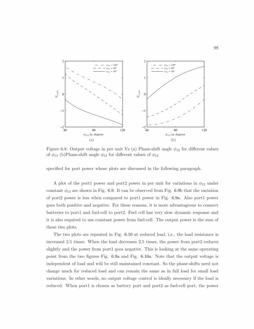
98
40 80 120−2
−1
0
1
2
φ12 in degrees
Vo
,pu
φ13 = 120o
φ13 = 90o
φ13 = 40o
(a)
40 80 120−2
−1
0
1
2
φ13 in degreesV
o,p
u
φ12 = 120o
φ12 = 90o
φ12 = 40o
(b)
Figure 6.8: Output voltage in per unit Vs (a) Phase-shift angle φ12 for different valuesof φ13 (b)Phase-shift angle φ13 for different values of φ12
specified for port power whose plots are discussed in the following paragraph.
A plot of the port1 power and port2 power in per unit for variations in φ12 under
constant φ13 are shown in Fig. 6.9. It can be observed from Fig. 6.9b that the variation
of port2 power is less when compared to port1 power in Fig. 6.9a. Also port1 power
goes both positive and negative. For these reasons, it is more advantageous to connect
batteries to port1 and fuel-cell to port2. Fuel cell has very slow dynamic response and
it is also required to use constant power from fuel-cell. The output power is the sum of
these two plots.
The two plots are repeated in Fig. 6.10 at reduced load, i.e., the load resistance is
increased 2.5 times. When the load decreases 2.5 times, the power from port2 reduces
slightly and the power from port1 goes negative. This is looking at the same operating
point from the two figures Fig. 6.9a and Fig. 6.10a. Note that the output voltage is
independent of load and will be still maintained constant. So the phase-shifts need not
change much for reduced load and can remain the same as in full load for small load
variations. In other words, no output voltage control is ideally necessary if the load is
reduced. When port1 is chosen as battery port and port2 as fuel-cell port, the power
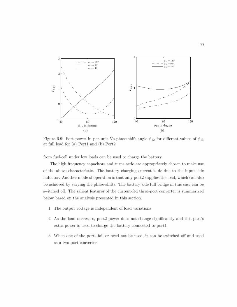
99
40 80 120−1
0
1
2
3
φ12 in degrees
P1
,pu
φ13 = 120o
φ13 = 90o
φ13 = 40o
(a)
40 80 1200
1
2
φ12 in degrees
P2
,pu
φ13 = 120o
φ13 = 90o
φ13 = 40o
(b)
Figure 6.9: Port power in per unit Vs phase-shift angle φ12 for different values of φ13
at full load for (a) Port1 and (b) Port2
from fuel-cell under low loads can be used to charge the battery.
The high frequency capacitors and turns ratio are appropriately chosen to make use
of the above characteristic. The battery charging current is dc due to the input side
inductor. Another mode of operation is that only port2 supplies the load, which can also
be achieved by varying the phase-shifts. The battery side full bridge in this case can be
switched off. The salient features of the current-fed three-port converter is summarized
below based on the analysis presented in this section.
1. The output voltage is independent of load variations
2. As the load decreases, port2 power does not change significantly and this port’s
extra power is used to charge the battery connected to port1
3. When one of the ports fail or need not be used, it can be switched off and used
as a two-port converter
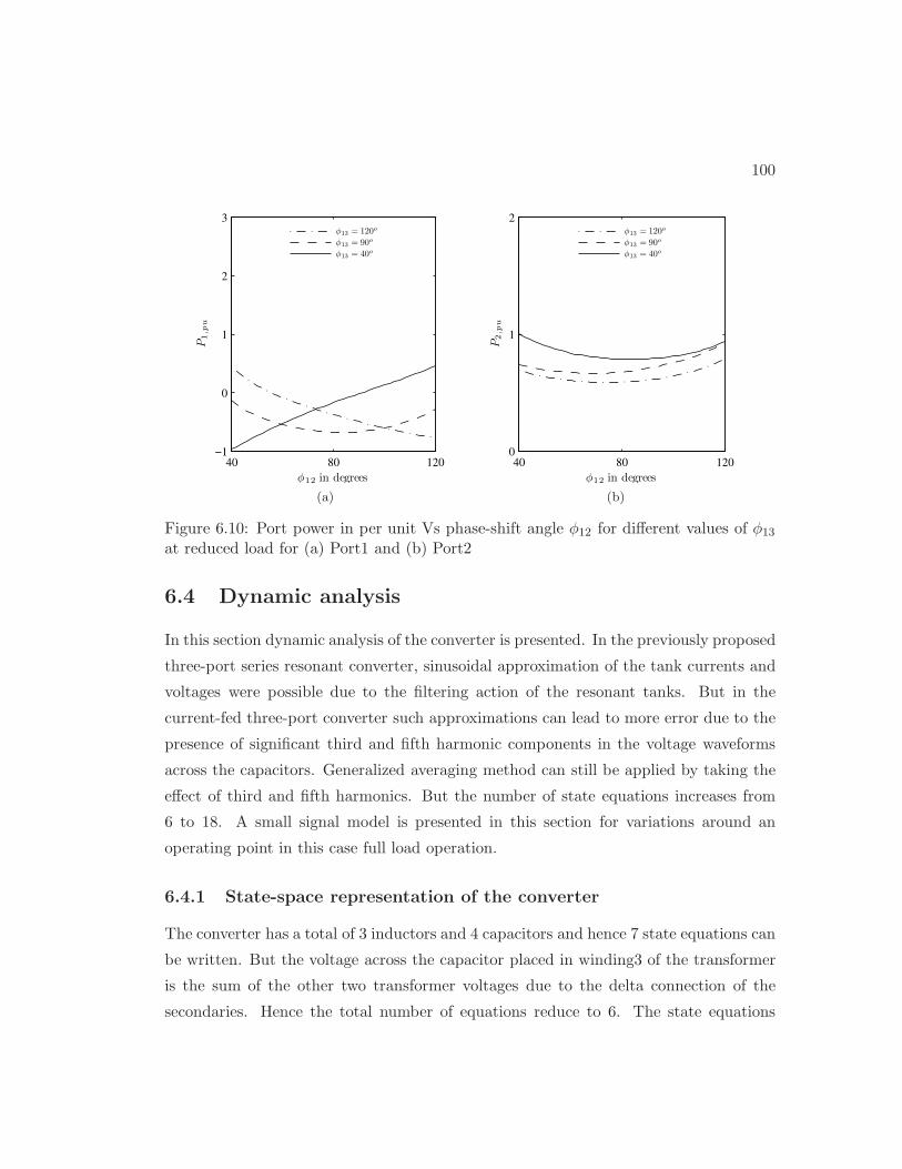
100
40 80 120−1
0
1
2
3
φ12 in degrees
P1
,pu
φ13 = 120o
φ13 = 90o
φ13 = 40o
(a)
40 80 1200
1
2
φ12 in degrees
P2
,pu
φ13 = 120o
φ13 = 90o
φ13 = 40o
(b)
Figure 6.10: Port power in per unit Vs phase-shift angle φ12 for different values of φ13
at reduced load for (a) Port1 and (b) Port2
6.4 Dynamic analysis
In this section dynamic analysis of the converter is presented. In the previously proposed
three-port series resonant converter, sinusoidal approximation of the tank currents and
voltages were possible due to the filtering action of the resonant tanks. But in the
current-fed three-port converter such approximations can lead to more error due to the
presence of significant third and fifth harmonic components in the voltage waveforms
across the capacitors. Generalized averaging method can still be applied by taking the
effect of third and fifth harmonics. But the number of state equations increases from
6 to 18. A small signal model is presented in this section for variations around an
operating point in this case full load operation.
6.4.1 State-space representation of the converter
The converter has a total of 3 inductors and 4 capacitors and hence 7 state equations can
be written. But the voltage across the capacitor placed in winding3 of the transformer
is the sum of the other two transformer voltages due to the delta connection of the
secondaries. Hence the total number of equations reduce to 6. The state equations

101
(6.30)-(6.35) are given below. The voltage polarity and current direction are indicated
in the Fig. 6.4. The on-state resistance rds(on) of the Mosfets are not included in the
equations.
vC1 = n1iL1
(
1
C ′1
+1
C ′2
)
sgn(sin(ωst)) −n2
C ′2
iL2sgn(sin(ωst − φ12))
− n3
C ′1
iL3sgn(sin(ωst − φ13)) (6.30)
vC2 = −n1
C ′2
iL1sgn(sin(ωst)) − n2iL2
(
1
C ′2
+1
C ′3
)
sgn(sin(ωst − φ12))
− n3
C ′3
iL3sgn(sin(ωst − φ13)) (6.31)
iL1 =V1
L1− n1
L1vC1sgn(sin(ωst)) (6.32)
iL2 =V2
L2− n2
L2vC2sgn(sin(ωst − φ12)) (6.33)
iL3 =n3
L3(vC1 + vC2) sgn(sin(ωst − φ13)) −
vo
L3(6.34)
vo =iL3
Co− vo
RCo(6.35)
6.4.2 Averaging
The dynamics of the voltages across the capacitors are very fast when compared to the
dynamics of the output and port currents. Using a similar time-scaling process used
in Chapter 3, the equations for the fast system can be reduced to a static equation.
To remove the switching function in the equation, averaging of the state equations is
performed. The port1 side inductor sees the average voltage v1r whose value can be
calculated from the steady-state equations since the dynamics of this variable is very
fast. Hence the averaged state equations are given in (6.36-6.39)
˙iL1 =V1
L1− n1n2
L1ωsC ′2
iL1 φ12
(
1 − |φ12|π
)
− n1n3
L1ωsC ′1
iL3 φ13
(
1 − |φ13|π
)
(6.36)
˙iL2 =V2
L2− n1n2
L2ωsC ′2
iL1 φ12
(
1 − |φ12|π
)

102
− n2n3
L2ωsC ′3
iL3 φ23
(
1 − |φ23|π
)
(6.37)
˙iL3 = − vo
L3+
n1n3
L3ωsC ′1
iL1 φ13
(
1 − |φ13|π
)
− n2n3
L3ωsC ′3
iL2 φ23
(
1 − |φ23|π
)
(6.38)
vo =iL3
Co− vo
RCo(6.39)
A small signal model is derived for perturbations in the load io and phase shifts
φ13, φ12 around the operating point. The small signal perturbations are defined as in
(6.40-6.42). The nominal values are defined with a subscript ’n’.
Define x = [iL1 iL2 iL3 vo]T
(6.40)
x = Xn + ˜x (6.41)
φ12 = φ12n + φ12; φ13 = φ13n + φ13 (6.42)
Ignoring the second order terms the small signal model can be derived as in (6.43).
The matrix A is obtained from (6.36-6.39).
˙x = A˜x + f1φ + f2io (6.43)
f1 =
− n1n3L1ωsC′
1X3nK13 − n1n2
L1ωsC′
2X2nK12
− n2n3L2ωsC′
3X3nK23
n2n3L2ωsC′
3X3nK23 + n1n2
L2ωsC′
2X1nK12
n1n3L3ωsC′
1X1nK13 + n2n3
L3ωsC′
3X2nK23 − n2n3
L3ωsC′
3X2nK23
(6.44)
K13 =
(
1 − 2|φ13n|π
)
; K12 =
(
1 − 2|φ12n|π
)
;
K23 =
(
1 − 2|φ23n|π
)
;
f2 = [0 0 0 0 1/Co]T (6.45)
Having obtained the small signal model with two inputs φ12, φ13 and the operating
point, controller can be designed to regulate the output voltage and one of the port
currents. The following section presents simulation results of the closed loop controller.
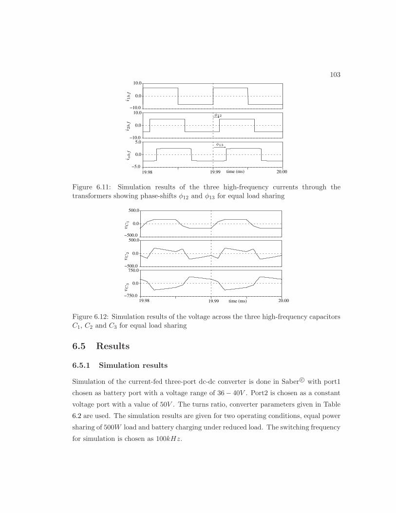
10310.0
0.0
−10.010.0
0.0
−10.05.0
0.0
−5.0
19.98 19.99 time (ms) 20.00
φ12
φ13
i 1h
fi 2
hf
i oh
f
Figure 6.11: Simulation results of the three high-frequency currents through thetransformers showing phase-shifts φ12 and φ13 for equal load sharing
time (ms)
500.0
0.0
500.0−500.0
0.0
−500.0750.0
0.0
−750.019.98 19.99 20.00
vC
2v
C1
vC
3
Figure 6.12: Simulation results of the voltage across the three high-frequency capacitorsC1, C2 and C3 for equal load sharing
6.5 Results
6.5.1 Simulation results
Simulation of the current-fed three-port dc-dc converter is done in Saber c© with port1
chosen as battery port with a voltage range of 36 − 40V . Port2 is chosen as a constant
voltage port with a value of 50V . The turns ratio, converter parameters given in Table
6.2 are used. The simulation results are given for two operating conditions, equal power
sharing of 500W load and battery charging under reduced load. The switching frequency
for simulation is chosen as 100kHz.
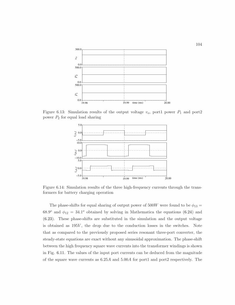
104
0.0500.0
0.0500.0
0.019.98 19.99 time (ms) 20.00
300.0
P1
P2
vo
Figure 6.13: Simulation results of the output voltage vo, port1 power P1 and port2power P2 for equal load sharing
10.0
0.0
−10.05.0
0.0
−5.019.98 19.99 time (ms) 20.00
5.0
0.0
−5.0
i 1h
fi 2
hf
i oh
f
Figure 6.14: Simulation results of the three high-frequency currents through the trans-formers for battery charging operation
The phase-shifts for equal sharing of output power of 500W were found to be φ13 =
68.9o and φ12 = 34.1o obtained by solving in Mathematica the equations (6.24) and
(6.23). These phase-shifts are substituted in the simulation and the output voltage
is obtained as 195V , the drop due to the conduction losses in the switches. Note
that as compared to the previously proposed series resonant three-port converter, the
steady-state equations are exact without any sinusoidal approximation. The phase-shift
between the high frequency square wave currents into the transformer windings is shown
in Fig. 6.11. The values of the input port currents can be deduced from the magnitude
of the square wave currents as 6.25A and 5.00A for port1 and port2 respectively. The
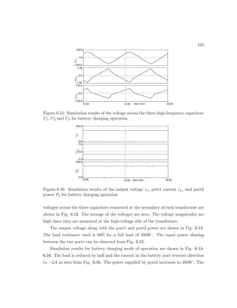
105
−1.0k750.0
0.0
−750.019.98 19.99 time (ms) 20.00
500.0
0.0
−500.01.0k
0.0v
C1
vC
2v
C3
Figure 6.15: Simulation results of the voltage across the three high-frequency capacitorsC1, C2 and C3 for battery charging operation
0.05.0
0.0
−5.0500.0
0.0
19.99 20.00time (ms)19.98
300.0
vo
P2
i L1
Figure 6.16: Simulation results of the output voltage vo, port1 current iL1 and port2power P2 for battery charging operation
voltages across the three capacitors connected at the secondary of each transformer are
shown in Fig. 6.12. The average of the voltages are zero. The voltage magnitudes are
high since they are measured at the high-voltage side of the transformer.
The output voltage along with the port1 and port2 power are shown in Fig. 6.13.
The load resistance used is 80Ω for a full load of 500W . The equal power sharing
between the two ports can be observed from Fig. 6.13.
Simulation results for battery charging mode of operation are shown in Fig. 6.14-
6.16. The load is reduced by half and the current in the battery port reverses direction
to −2A as seen from Fig. 6.16. The power supplied by port2 increases to 350W . The
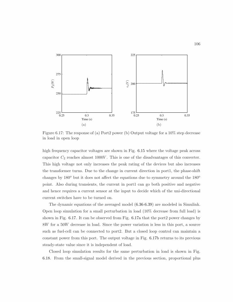
106
0.25 0.3 0.35225
250
275
300
Time (s)
P2(W
)
(a)
0.25 0.3 0.35175
200
225
Time (s)
v o(V
)(b)
Figure 6.17: The response of (a) Port2 power (b) Output voltage for a 10% step decreasein load in open loop
high frequency capacitor voltages are shown in Fig. 6.15 where the voltage peak across
capacitor C2 reaches almost 1000V . This is one of the disadvantages of this converter.
This high voltage not only increases the peak rating of the devices but also increases
the transformer turns. Due to the change in current direction in port1, the phase-shift
changes by 180o but it does not affect the equations due to symmetry around the 180o
point. Also during transients, the current in port1 can go both positive and negative
and hence requires a current sensor at the input to decide which of the uni-directional
current switches have to be turned on.
The dynamic equations of the averaged model (6.36-6.39) are modeled in Simulink.
Open loop simulation for a small perturbation in load (10% decrease from full load) is
shown in Fig. 6.17. It can be observed from Fig. 6.17a that the port2 power changes by
8W for a 50W decrease in load. Since the power variation is less in this port, a source
such as fuel-cell can be connected to port2. But a closed loop control can maintain a
constant power from this port. The output voltage in Fig. 6.17b returns to its previous
steady-state value since it is independent of load.
Closed loop simulation results for the same perturbation in load is shown in Fig.
6.18. From the small-signal model derived in the previous section, proportional plus
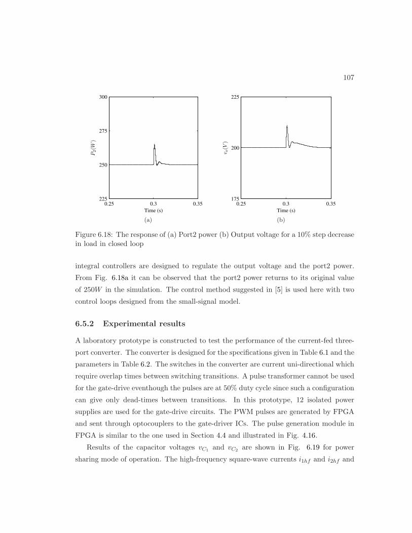
107
0.25 0.3 0.35225
250
275
300
Time (s)
P2(W
)
(a)
0.25 0.3 0.35175
200
225
Time (s)
v o(V
)(b)
Figure 6.18: The response of (a) Port2 power (b) Output voltage for a 10% step decreasein load in closed loop
integral controllers are designed to regulate the output voltage and the port2 power.
From Fig. 6.18a it can be observed that the port2 power returns to its original value
of 250W in the simulation. The control method suggested in [5] is used here with two
control loops designed from the small-signal model.
6.5.2 Experimental results
A laboratory prototype is constructed to test the performance of the current-fed three-
port converter. The converter is designed for the specifications given in Table 6.1 and the
parameters in Table 6.2. The switches in the converter are current uni-directional which
require overlap times between switching transitions. A pulse transformer cannot be used
for the gate-drive eventhough the pulses are at 50% duty cycle since such a configuration
can give only dead-times between transitions. In this prototype, 12 isolated power
supplies are used for the gate-drive circuits. The PWM pulses are generated by FPGA
and sent through optocouplers to the gate-driver ICs. The pulse generation module in
FPGA is similar to the one used in Section 4.4 and illustrated in Fig. 4.16.
Results of the capacitor voltages vC1 and vC2 are shown in Fig. 6.19 for power
sharing mode of operation. The high-frequency square-wave currents i1hf and i2hf and
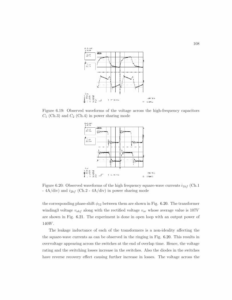
108
Figure 6.19: Observed waveforms of the voltage across the high-frequency capacitorsC1 (Ch.3) and C2 (Ch.4) in power sharing mode
Figure 6.20: Observed waveforms of the high frequency square-wave currents i1hf (Ch.1- 4A/div) and i2hf (Ch.2 - 4A/div) in power sharing mode
the corresponding phase-shift φ12 between them are shown in Fig. 6.20. The transformer
winding3 voltage vohf along with the rectified voltage vor whose average value is 107V
are shown in Fig. 6.21. The experiment is done in open loop with an output power of
140W .
The leakage inductance of each of the transformers is a non-ideality affecting the
the square-wave currents as can be observed in the ringing in Fig. 6.20. This results in
overvoltage appearing across the switches at the end of overlap time. Hence, the voltage
rating and the switching losses increase in the switches. Also the diodes in the switches
have reverse recovery effect causing further increase in losses. The voltage across the
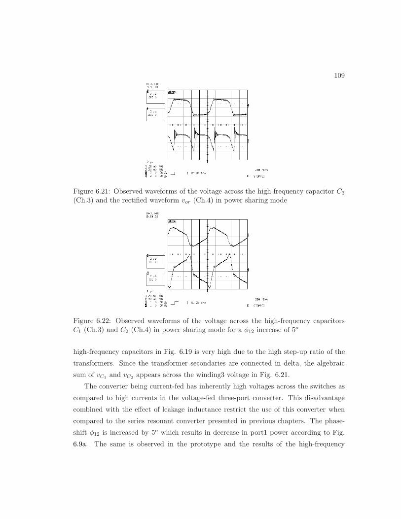
109
Figure 6.21: Observed waveforms of the voltage across the high-frequency capacitor C3
(Ch.3) and the rectified waveform vor (Ch.4) in power sharing mode
Figure 6.22: Observed waveforms of the voltage across the high-frequency capacitorsC1 (Ch.3) and C2 (Ch.4) in power sharing mode for a φ12 increase of 5o
high-frequency capacitors in Fig. 6.19 is very high due to the high step-up ratio of the
transformers. Since the transformer secondaries are connected in delta, the algebraic
sum of vC1 and vC2 appears across the winding3 voltage in Fig. 6.21.
The converter being current-fed has inherently high voltages across the switches as
compared to high currents in the voltage-fed three-port converter. This disadvantage
combined with the effect of leakage inductance restrict the use of this converter when
compared to the series resonant converter presented in previous chapters. The phase-
shift φ12 is increased by 5o which results in decrease in port1 power according to Fig.
6.9a. The same is observed in the prototype and the results of the high-frequency

110
voltages across the capacitors C1 and C2 for this operating point are shown in Fig. 6.22
where the voltage vC2 has a higher peak value. The output voltage drops by 5V in this
case.
6.6 Conclusion
In this Chapter, the current-fed three-port dc-dc converter is proposed. Steady-state
analysis of the converter is presented with phase-shifts between the active bridges as
the control variables. It can be observed that the output voltage is independent of
the load resistance. Also, as the load reduces the power from port2 remains almost
constant and the current in port1 reverses direction. Small-signal model around a
steady-state operating point is presented and simulation results of the controller are
given. Simulation results of the converter in power sharing mode and battery charging
mode are presented.
Chapter 7
Conclusion
Renewable energy sources such as fuel-cell, PV array are being increasingly used for
stand-alone residential, commercial and automobile applications. Multi-port dc-dc con-
verters are needed to interface the sources and the load along with energy storage in
such applications. This thesis addresses this need by proposing two converter topolo-
gies. Both the topologies use high-frequency ac-link and hence have the advantages of
reduced size, reduced power conversion stages and reduced part count when compared
to conventional dc-link based systems. Some of the important conclusions in the work
done in this thesis are discussed in the following section.
7.1 Conclusion
7.1.1 Series resonant three-port converter
In Chapter 2, a three-port series resonant converter [43] is proposed. It has two series
resonant tanks and a three-winding transformer. Bi-directional power flow in all ports
is achieved by phase-shift control of the three active bridges. Detailed analysis of the
converter to determine the steady-state expressions of output voltage, port power, peak
tank currents, peak tank voltages and soft-switching operation boundary is presented.
The existing high-frequency ac-link topology for three-port converter uses only induc-
tances, which includes the leakage inductances of the three-winding transformer, for
power flow control. Since the power flow between ports is inversely proportional to the
111

112
impedance offered by the leakage inductance and the external inductance, impedance
has to be low at high power levels. To get realizable inductance values equal to or
more than the leakage inductance of the transformer, the switching frequency has to be
reduced. Hence the selection of switching frequency is not independent of the value of
inductance. The proposed series-resonant converter has more freedom in choosing real-
izable inductance values and the switching frequency, independent of each other. Such
a converter can operate at higher switching frequencies for medium and high-power
converters. A detailed comparison with the existing three-port converter in literature
is presented in Chapter 4.
The tank capacitors in the series resonant converter play an additional role of block-
ing dc voltages caused because of difference in dead times and characteristics of the
switches used in the active bridges. Whereas in existing three-port converter, the mag-
netizing inductance has to be reduced significantly to prevent saturation of the trans-
former. This also affects the power flow calculations since it changes the impedance in
the power flow expressions. A detailed analysis of the three-winding transformer and
its effect on the operation of the series resonant three-port converter is discussed in Sec-
tion 2.5.1 and Section 4.2.3. The analysis concludes that the effect of the magnetizing
inductance and the third winding leakage inductance on the power flow between ports
can be reduced by designing the quality factors appropriately.
The steady-state analysis presented in Chapter 2 uses sinusoidal approximation.
Such an approximation is valid due to filtering action of the series resonant tanks on the
harmonics of the square wave applied voltages. With this approximation the derivation
of the steady-state expressions are simplified. The expressions are converted to per unit
and the design procedure is explained in Chapter 4. The design procedure gives details
on selection of the voltage conversion ratios and its effect on soft-switching operating
boundary. From the design procedure, it can be concluded that the three-port converter
can do soft-switching in all switches provided that the voltage conversion ratios are
chosen to be unity. Also the procedure ensures operation in all three modes, power
sharing, battery charging and regenerative load.
Dynamic analysis of the converter using generalized averaging method is explained
in Chapter 3. Two different time scales are identified which simplifies the controller
design. Methods to control the output voltage in closed loop with a fixed reference for
113
one of the port currents are explained in this Chapter. The controller is implemented
in FPGA in a laboratory prototype and the results are given in Chapter 4. These
experimental results augment the analysis and simulation results.
The series-resonant three-port converter is modified for uni-directional load appli-
cations [44, 45] in Chapter 5. Due to the presence of diode bridge at the output, the
phase-shift between the active bridges and the diode bridge is fixed and not controllable.
Two phase-shift control variables are proposed for this converter. A center modulation
technique is adopted to remove the interdependence on the phase-shifts between bridges
and between legs in a single bridge. Using this control technique, bi-directional power
flow in the other two ports are achieved. Detailed analysis are presented to determine
the modified output voltage, port power, tank voltages, tank currents and soft-switching
operating boundary. From the analysis it can be concluded that soft-switching opera-
tion in all the switches is not possible in this converter. Bi-directional power flow and
control using phase-shifts are verified both in simulation and hardware prototype and
the results are presented. Analytical expressions for peak tank currents and voltages
including transformer rating are difficult to derive due to the presence of diode bridge
and hence simulation results at various operating points are given in this Chapter.
7.1.2 Current-fed three-port converter
A current-fed three-port converter [46] is proposed in Chapter 6. This converter has
inductors at the input and hence act as current ports. This ensures dc currents at
the ports and thereby eliminates the need of capacitive filters as in the series resonant
three-port converter. This converter is the dual of the existing three-port converter
with only inductances. In this converter the square wave currents are phase-shifted
from each other to control power flow between ports. Three separate transformers are
needed and their secondaries are connected in delta. Detailed analysis of the converter is
presented in this Chapter to determine the output voltage and power flow expressions.
It is observed from the analysis that the output voltage is independent of the load
resistance as opposed to the series resonant converter. Bi-directional power flow in the
battery port is possible and verified through analysis and simulation.
The converter being current-fed uses uni-directional current switches and hence re-
quires one Mosfet and one diode for each switch. This increases the semiconductor

114
switch count. Also for battery port, the diode needs to be replaced by another Mos-
fet to enable current direction reversal during battery charging. Since capacitors are
used in the high-frequency side, the voltages across the capacitors increase two or three
times the nominal voltage of the ports. This increases the voltage rating of the devices.
These are some of the disadvantages of this converter over the series resonant three-port
converter.
Sinusoidal approximation is not possible in this converter due to the high third and
fifth harmonic content in the voltage waveforms. Hence when the generalized averaging
theory is applied, the number of state equations increase three-fold. A small-signal
analysis around a steady-state operating point is presented in Chapter 6. Simulation
results of the converter in closed loop are presented for variations around the steady-
state operating point.
7.2 Future work
The future scope of this work can include the following,
• Parallel resonant, LCC resonant and self-oscillating resonant circuits have unique
advantages in two-port configurations. These topologies can be extended for three-
port applications.
• This thesis discusses dc-dc-dc power conversion. Rectifiers or inverters are needed
as additional power conversion stages to interface ac sources and ac loads. High
frequency ac-link based single-stage power conversion can also be explored for ac-
dc-ac three-port converter. Modified phase-shift modulation techniques need to
be proposed for ac-dc-ac interfaces.
• The application scope of this three-port converter can be extended to power flow
control devices in residential and commercial buildings, uninterruptible power sup-
plies and high-power automobile applications.
• This thesis discusses three-port converter and the same principle can be extended
to four-port or multi-port converters. The analysis and control methods for such
configurations have to be explored.

Bibliography
[1] (2009) Solar america cities. U.S. Department of Energy. [Online]. Available:
http://solaramericacities.energy.gov/
[2] “Final report on energy storage technologies,” U.S. Department of Energy, Elec-
tricity Advisory Committee, Dec. 2008.
[3] (2009) Fuel cell vehicles. U.S. Department of Energy. [Online]. Available:
http://www.fueleconomy.gov/feg/fuelcell.shtml
[4] C. Zhao and J. W. Kolar, “A novel three-phase three-port ups employing a single
high-frquency isolation transformer,” in Proc. IEEE Power Electronics Specialists
Conference (PESC’04), 2004, pp. 4135–4141.
[5] H. Tao, A. Kotsopulos, J. L. Duarte, and M. A. M. Hendrix, “Family of multiport
bidirectional dc-dc converters,” IEE Proceedings in Electric Power Applications,
vol. 153, no. 15, pp. 451–458, May 2006.
[6] M. H. Kheraluwala, R. W. Gascoigne, D. M. Divan, and E. D. Baumann, “Per-
formance characterization of a high-power dual active bridge dc-to-dc converter,”
IEEE Trans. Ind. Appl., vol. 28, no. 6, pp. 1294–1300, Nov. 1992.
[7] R. L. Steigerwald, “Half bridge resonant converter topologies,” IEEE Trans. Power
Electron., vol. 3, no. 2, pp. 173–182, Apr. 1988.
[8] P. Jain and H. Pinheiro, “Hybrid high frequency ac power distribution architecture
for telecommunication systems,” Aerospace and Electronic Systems, IEEE Trans-
actions on, vol. 35, no. 1, pp. 138–147, Jan 1999.
115

116
[9] Z. Ye, P. Jain, and P. Sen, “A full-bridge resonant inverter with modified phase-
shift modulation for high-frequency ac power distribution systems,” IEEE Trans.
Ind. Electron., vol. 54, no. 5, pp. 2831–2845, Oct. 2007.
[10] J. L. Duarte, M. A. M. Hendrix, and M. G. Simoes, “Three-port bi-directional
converter for hybrid fuel cell systems,” IEEE Trans. Power Electron., vol. 22, no. 2,
pp. 480–487, Mar. 2007.
[11] D. Maksimovic, R. Erickson, and C. Griesbach, “Modeling of cross-regulation in
converters containing coupled inductors,” IEEE Trans. Power Electron., vol. 15,
no. 4, pp. 607–615, Jul 2000.
[12] H. Tao, J. Duarte, and M. Hendrix, “Three-port triple-half-bridge bidirectional
converter with zero-voltage switching,” IEEE Trans. Power Electron., vol. 23, no. 2,
pp. 782–792, March 2008.
[13] H. Tao, A. Kotsopoulos, J. Duarte, and M. Hendrix, “Transformer-coupled multi-
port zvs bidirectional dcdc converter with wide input range,” IEEE Trans. Power
Electron., vol. 23, no. 2, pp. 771–781, March 2008.
[14] H. Tao, J. L. Duarte, and M. A. M. Hendrix, “High-power three-port three-phase
bidirectional dc-dc converter,” in Proc. IEEE Industry Applications Society 42nd
Annual Meeting (IAS’07), 2007, pp. 2022–2029.
[15] D. Liu and H. Liu, “A zvs bi-directional dc-dc converter for multiple energy storage
elements,” IEEE Trans. Power Electron., vol. 21, no. 5, pp. 1513–1517, Sep. 2006.
[16] B. Dobbs and P. Chapman, “A multiple-input dc-dc converter topology,” Power
Electronics Letters, IEEE, vol. 1, no. 1, pp. 6–9, March 2003.
[17] H. Matsuo, K. Kobayashi, Y. Sekine, M. Asano, and L. Wenzhong, “Novel solar
cell power supply system using the multiple-input dc-dc converter,” in Telecommu-
nications Energy Conference, 1998. INTELEC. Twentieth International, 1998, pp.
797–802.

117
[18] H. Al-Atrash, F. Tian, and I. Batarseh, “Tri-modal half-bridge converter topology
for three-port interface,” IEEE Trans. Power Electron., vol. 22, no. 1, pp. 341–345,
Jan. 2007.
[19] H. Pinheiro and P. K. Jain, “Series-parallel resonant ups with capacitive output dc
bus filter for powering hfc networks,” IEEE Trans. Power Electron., vol. 17, no. 6,
pp. 971–979, Nov. 2002.
[20] H. Al-Atrash, F. Tian, and I. Batarseh, “Tri-modal half-bridge converter topology
for three-port interface,” IEEE Trans. Power Electron., vol. 22, no. 1, pp. 341–345,
Jan. 2007.
[21] S. Inoue and H. Akagi, “A bidirectional isolated dcdc converter as a core circuit
of the next-generation medium-voltage power conversion system,” IEEE Trans.
Power Electron., vol. 22, no. 2, pp. 535–542, March 2007.
[22] F. Z. Peng, M. Shen, and K. Holland, “Application of z-source inverter for traction
drive of fuel cellbattery hybrid electric vehicles,” IEEE Trans. Power Electron.,
vol. 22, no. 3, pp. 1054–1061, May 2007.
[23] Y.-M. Chen, Y.-C. Liu, S.-C. Hung, and C.-S. Cheng, “Multi-input inverter for grid-
connected hybrid pv/wind power system,” IEEE Trans. Power Electron., vol. 22,
no. 3, pp. 1070–1077, May 2007.
[24] G.-J. Su and L. Tang, “A multiphase, modular, bidirectional, triple-voltage dcdc
converter for hybrid and fuel cell vehicle power systems,” IEEE Trans. Power
Electron., vol. 23, no. 6, pp. 3035–3046, Nov. 2008.
[25] X. Li and A. K. S. Bhat, “Ac equivalent circuit analysis for high-frequency isolated
dual-bridge series resonant dc/dc converter,” in Proc. IEEE Power Electronics
Specialists Conference (PESC’08), 2008, pp. 238–244.
[26] B. S. Nathan, “Analysis, simulation and design of series resonant converter for high
voltage applications,” M.Sc.(Engg.) thesis, Indian Institute of Science, Bangalore,
India, Dec. 1999.

118
[27] S. Sanders, J. Noworolski, X. Liu, and G. Verghese, “Generalized averaging method
for power conversion circuits,” IEEE Trans. Power Electron., vol. 6, no. 2, pp. 251–
259, Apr 1991.
[28] J. Carrasco, E. Galvan, G. Valderrama, R. Ortega, and A. Stankovic, “Analysis and
experimentation of nonlinear adaptive controllers for the series resonant converter,”
IEEE Trans. Power Electron., vol. 15, no. 3, pp. 536–544, May 2000.
[29] A. Stankovic, “A dissipativity-based controller for series resonant dc/dc convert-
ers,” in Proc. IEEE Power Electronics Specialists Conference (PESC’96), 1996, pp.
1844–1849.
[30] D. Maksimovic, A. Stankovic, V. Thottuvelil, and G. Verghese, “Modeling and
simulation of power electronic converters,” Proc. IEEE, vol. 89, no. 6, pp. 898–912,
Jun 2001.
[31] A. Stankovic, D. Perreault, and K. Sato, “Synthesis of dissipative nonlinear con-
trollers for series resonant dc/dc converters,” IEEE Trans. Power Electron., vol. 14,
no. 4, pp. 673–682, Jul 1999.
[32] C. Jacobson, A. Stankovic, and G. Tadmor, “Design of robust controllers for reso-
nant dc/dc converters,” Sep 1995, pp. 360–365.
[33] Y. Lu, K. Cheng, S. Ho, and J. Pan, “Passivity-based control of a phase-shifted
resonant converter,” Electric Power Applications, IEE Proceedings -, vol. 152, no. 6,
pp. 1509–1515, Nov. 2005.
[34] H. K. Khalil, Nonlinear Systems, 3rd ed. Prentice Hall, 2002.
[35] (2009) Nuvera fuel cells, powerflow. [Online]. Available:
http://www.nuvera.com/products/powerflow.php
[36] O. Bitsche and G. Gutmann, “Systems for hybrid cars,” Journal of Power Sources,
vol. 127, no. 1-2, pp. 8 – 15, 2004, eighth Ulmer Electrochemische Tage.
[37] N. Mohan, T. M. Undeland, and W. P. Robbins, Power Electronics Converters,
Applications and Design, 3rd ed. John Wiley and Sons, Inc, 2003.

119
[38] R. Middlebrook and S. Cuk, Advances in switched-mode power conversion, Vols 1
and 2, 1st ed. Teslaco, 1983.
[39] (2009) Digilent basys board reference manual. [Online]. Available:
http://www.digilentinc.com/Data/Products/BASYS/BASYS C rm.pdf
[40] H. Krishnaswami and V. Ramanarayanan, “Control of high-frequency ac link elec-
tronic transformer,” Electric Power Applications, IEE Proceedings -, vol. 152, no. 3,
pp. 509–516, May 2005.
[41] R. W. Erickson and D. Maksimovic, Fundamentals of Power Electronics, 2nd ed.
Kluwer Academic Publishers, 2000.
[42] M. Ehsani, I. Husain, and M. Bilgic, “Inverse dual converter (idc) for high power
dc-dc applications,” in Power Electronics Specialists Conference, 1990. PESC ’90
Record., 21st Annual IEEE, Jun 1990, pp. 814–821.
[43] H. Krishnaswami and N. Mohan, “Three-port series-resonant dc-dc converter to in-
terface renewable energy sources with bi-directional load and energy storage ports,”
IEEE Trans. Power Electron., accepted for publication.
[44] H. Krishnaswami and N. Mohan, “Constant switching frequency series resonant
three-port bi-directional dc-dc converter,” in Proc. IEEE Power Electronics Spe-
cialists Conference (PESC’08), 2008, pp. 1640–1645.
[45] H. Krishnaswami and N. Mohan, “Simulation model of a three-port bi-directional
series resonant dc-dc converter to determine component specifications,” in Proc.
SCS Grand Challenges in Modeling and Simulation (GCMS’08), 2008.
[46] H. Krishnaswami and N. Mohan, “A current-fed three-port bi-directional dc-dc
converter,” in Proc. IEEE International Telecommunications Energy Conference
(INTELEC’07), 2007, pp. 523–526.
Related Documents