29/11/01 7-1 Chapter 7 DC/DC CONVERTERS DC/DC converters are the most common type of power conversion circuit. They change one DC voltage (usually unregulated) to another DC voltage (usually regulated). Many DC/DC converters are embedded within AC/DC power supplies. Even most AC/DC power supplies consist of a diode bridge to change the AC input voltage into an unregulated high voltage DC followed by a DC/DC converter to produce a regulated, low voltage DC output.

Welcome message from author
This document is posted to help you gain knowledge. Please leave a comment to let me know what you think about it! Share it to your friends and learn new things together.
Transcript

29/11/01
7-1
Chapter 7
DC/DC CONVERTERS
DC/DC converters are the most common type of power conversion circuit. They change one DC voltage (usually unregulated) to another DC voltage (usually regulated). Many DC/DC converters are embedded within AC/DC power supplies. Even most AC/DC power supplies consist of a diode bridge to change the AC input voltage into an unregulated high voltage DC followed by a DC/DC converter to produce a regulated, low voltage DC output.

29/11/01
7-2
7.1 BUCK CONVERTER (also known as a Buck Regulator)
The basic schematic circuit diagram for a Buck Converter is shown in Figure 7.1.
V
L
C O
IO
VD
VS
+
- D
iL
S
(Semiconductor Switch)
RO
Figure 7.1 Basic Schematic Diagram for a Buck Converter
Switch S is turned on for t1seconds and then turned off for t2 seconds such that:
t1 + t2 = Τ (7.1-1)
where T is the period for one switching cycle. The basic waveforms are shown in Figure 7.2

29/11/01
7-3
VS
VD
t1 t2
t
T
t
IOI
1
I2
∆I
iL
VO
Mode I Mode II
Figure 7.2 Basic Waveforms for the Buck Converter
We can assume that the output capacitor C is large enough such that VO is constant and therefore IO is also constant during the switching period.
When the switch S is turned on at t = 0, diode D becomes reverse biased and acts as an open circuit. This is referred to a Mode I and the equivalent circuit for this mode is shown in Figure 7.3.
29/11/01
7-4
V
L
C O
IO
VS
+
-
iL
RO
V L
iC
Figure 7.3 Basic Schematic Diagram for Buck Converter During Mode I
During this mode, the governing equation is:
VL = VS - VO = Li
tL∂
∂ (7.1-2)
Solve for
iL(t) = I1 + (VS- VO)t
L (7.1-3)
Where I1 is the initial current in inductor L at t=0.
The above equation is valid until the switch S is turned off at t=t1 at which time
the inductor current is defined as I2 , the inductor current current at the end of
Mode I, where:
I2 = iL(t1) =I1 + (VS- VO)t1
L (7.1-4)
When switch S is turned off, the inductor current continues to flow through diode D. The interval during which the switch S is turned off is referred to as Mode II. The equivalent circuit for this mode is shown in Figure 7.4:

29/11/01
7-5
V
L
C O
IOi
L
RO
V L
iC
D (Conducting)
Figure 7.4 Basic Schematic Diagram for Buck Converter During Mode II
During this mode the governing equation is:
VL = -VO = Li
tL∂
∂ (7.1-5)
Solve the above equation for
iL(t) = I2 - VOt
L (7.1-6)
The switch will turn on again at t=t2 at which time the cycle will be back to the
same conditions as at t=0 (assuming steady state has been reached). Therefore the inductor current at t=t2 will be same as the initial current, I1 , at t=0 where:
I1 =iL(t2) = I2 - V0t2
L (7.1-7)
In the steady state I1 from the end of Mode II will be equal to I1 from the
beginning of Mode I. Similarly, I2 at the end of Mode I will be equal to I2 at the
beginning of Mode II.
We can obtain two expressions for I2 -I1 :
a) from the end of Mode I;
I2 - I1 = (VS- VO)t1
L (7.1-8)

29/11/01
7-6
b) from the end of Mode II;
I2 - I1 = VOt2
L (7.1-9)
Solve the above equations for
VOt2
L = (VS -VO)t1
L (7.1-10)
Define the duty cycle, δ ,as;
δ = t1T (7.1-11)
Where T = t1 + t2 (7.1-12)
∴ t1 = δT (7.1-13)
and t2 = (1-δ)T (7.1-14)
Substitute for t1 and t2 into equation (7.1-10) to obtain:
VO(1-δ) =(VS - VO )δ (7.1-15)
The above equation can be simplified to;
VO=δVS (7.1-16)
Also, define the current swing, ∆I, as:
∆I = I2 -I1 = V0t2
L (7.1-17)
or
∆I = V0(1-δ)
fL (7.1-18)
where f = 1/T = the switching frequency
Also, if the capacitor C is lossless then the DC current through it will be zero,
29/11/01
7-7
and:
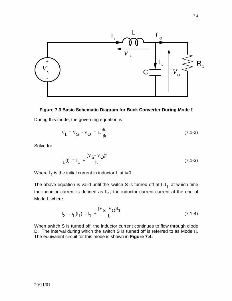
I0 = average (IL ) = (I1 +I2 )/2 (7.1-19)
Solve for
I1 = I0 -
∆I2
I2 = I0 + ∆I2
(7.1-20)
Also expression for the capacitor current, iC , can be derived as follows;
iC(t) = iL(t) - I0 (7.1-21)
= I1 - I0 + (VS -VO)t
L during Mode I (7.1-22)
= - ∆I2 +
∆Itt1
(7.1-23)
and iC(t) = ∆I2 -
∆Itt2
during Mode II (7.1-24)
Therefore the peak to peak ripple current in the capacitor can be determined
from the above equations:
∆IC = V0(1-δ)
fL (7.1-25)
Also the peak to peak ripple voltage in ∆V0 can be determined by integrating the
ripple current in the output capacitor;
∆V0 = ∆VC = 1
Ci (t) tct
2
t
1
1 ∂ + 1
Ci (t) tc0
t
22 ∂ (7.1-26)

29/11/01
7-8
= 1
C
I
2
It
tt
1t
2
t
1
1 ∆ ∆−
∂ +
1
C
I
2
It
tt
20
t
22
∆ ∆−
∂ (7.1-27)
= ∆I2C
-t + t2
t1
t1
t12
+ ∆I2C
t - t2
t2
t22
0
(7.1-28)
= ∆ ∆I
2C
t
4
I
2C
t
41 2
+
(7.1-29)
= ∆I8C(t1 + t2) (7.1-30)
∴ ∆ VC = ∆I8C T =
∆I8fC peak to peak (7.1-31)
Also one can substitute for ∆I = V0(1-δ)
fL to obtain;
∆VC = V0(1-δ)
8f2LC (7.1-32)
Note the above expression for peak to peak ripple does not include "switching spikes" which appear on the output due to high frequency components of the switching waveform which get through the L and C of the output filter.
In particular, the major component of ripple is often due to the equivalent series resistance, ESR , in the output capacitor combined with the ripple current in this
capacitor. This component of output ripple is referred to as ∆VR , where;
∆VR = ∆IC ESR peak to peak (7.1-33)
Usually one of the above, ∆VC or ∆VR , dominates. At high frequencies it’s
∆VR , at low frequencies it’s ∆VC .
Note that in the entire preceding analysis it was assumed that the inductor current, iL , never went to zero.

29/11/01
7-9
i.e. I1 > 0 (7.1-34)
Substitute for I1 = I0 - V0(1-δ)
2fL > 0 (7.1-35)
and solve for
L > V0(1-δ)
2fI0 (7.1-36)
This is defined as the critical inductance, LC , where;
LC = V0(1-δ)
2fI0 (7.1-37)
This gives us the critical, minimum, value for L that will maintain the above equations for ∆I, ∆VC , I1 , I2 and VO .
Conversely, for any given value of L we can solve for the critical, minimum, value of I0 ;
Imin. > V0(1-δ)
2fL (7.1-38)
This gives us the critical, minimum, value for load on the Buck Converter, I0 , that
will maintain the above equations for ∆I, ∆VC , I1 , I2 and VO .
Also, for resistive loads;
IO = VORO
= δVSRO
(7.1-39)
And the output power PO , can be determined;

29/11/01
7-10
PO = IO VO = δ2V
2S
RO (7.1-40)
For an ideal (lossless) Buck Converter, the input power will be equal to the output power;
Pin = PO (7.1-41)
or;
Iin VS = δ2V
2S
RO (7.1-42)
Solve for;
Iin = δ2VSRO
= δIO (7.1-43)
Also the bulk input impedance, Rin , can be determined, where;
Rin = VS /Iin = RO
δ2 (7.1-44)
Therefore a buck converter acts like a DC to DC transformer with a turns ratio of δ.

29/11/01
7-11
Example Problem 7-1 Design a Buck Converter to meet the following requirements: VS = 300 Vdc ± 50 Vdc VO = 50 Vdc
Maximum ripple = 200 mV peak to peak IO = 1 Amp minimimum, 25 A maximum
Switching frequency is 200 kHz Determine: a) The duty cycle, δ, at minimum, nominal and maximum input voltage. b) The critical inductance required and average and peak current rating for the inductor. c) The peak to peak ripple current in the output capacitor. d) The output capacitance required, assuming zero ESR .
e) The output capacitance required assuming an ESR of 0.8 Ω per 1000µF can.
f) The peak voltage and current for the diode and transistor switch. Solution:
a) VO = δVS therefore δ = VOVS
at minimum VS δ = 50/(300 - 50) = 0.2 at nominal VS δ = 50/300 = 0.167 at maximum VS δ = 50/(300 + 50) = 0.143
b) LC = V0(1-δ)
2fI0 for worst case δ = minimum and IO = minimum
Therefore:
LC = 50 1 0143
2 200 10 13
× −× × ×
( . ) = 107 µH
I = IO = 25 A worst case
I = I2 = I0 + ∆I
2
and ∆I = V0(1-δ)
fLC =
50 1 0143
200 10 107 103 6
× −× × × −
( . ) = 2 A
Substitute into the expression for to obtain:
I = I0 + ∆I
2 = 25 +
2
2 = 26 A
c) ∆I C = ∆I = 2.0 A

29/11/01
7-12
d) ∆VC = V0(1-δ)
8f2LC
Solve for C = V(1- )
8f L V2c
δ∆
= 50 1 0143
8 200 10 107 10 0 23 2 6
× −
× × × × ×−
( . )
.
= 6.25 µF
e) ∆VR = ∆IC ETotalSR
Solve for:
ETotalSR =
∆VR∆IC
Where ETotalSR represents the total equivalent E
SR of all the capacitors in the
output filter. Typically this consists of a number of capacitor "cans" connected in parallel, and thus:
ETotalSR =
ESRNC
Where NC represents the number of cans
Therefore solve for:
NC = E
SR
ETotalSR
= E
SR ∆IC∆VR
= 08 2
0 2
.
.
×= 8
Total capacitance CTotal = NC CC where CC is the capacitance per can
Therefore CTotal = 8 × 1000 = 8000 µF f) Peak voltage for diode and transistor is: VD = VQ =VS = 300 + 50 = 350 V worst case
Peak current for diode and transistor is: ID = IQ = I2 = 26 A worst case
29/11/01
7-13
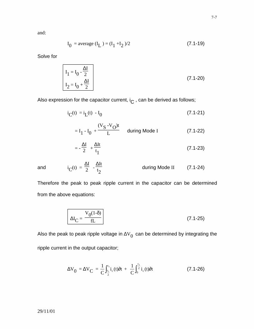
7.2 BOOST CONVERTER (also known as a Boost Regulator)
The basic schematic circuit diagram for a Boost Converter is shown in Figure 7.5.
V
L
C O
IO
VDV
S
+
-
Di L
S(Semiconductor Switch)
RO
FIGURE 7.5 Basic Schematic Diagram For a Boost Converter
Switch S is turned on for t1 seconds and then turned off for t2 seconds such
that:
t1 + t2 = Τ (7.2-1)
where Τ is the period for one switching cycle.
We can assume that the output capacitor C is large enough such that Vo is
constant and therefore Io is also constant during the switching period.
When the switch S is turned on at t=0, diode D becomes reverse biased and acts as an open circuit. This is referred to a Mode I and the equivalent circuit for this mode is shown in Figure 7.6

29/11/01
7-14
V
L
C O
IO
VS
+
-
i L
S(Semiconductor Switch)
RO
FIGURE 7.6 Equivalent Circuit During Mode I
During this mode, the governing equation is:
VL = VS = Li
tL∂
∂ (7.2-2)
Solve for
iL(t) = I1 + VSt
L (7.2-3)
Where I1 is the initial current in inductor L at t=0.
The above equation is valid until the switch S is turned off at t=t1 at which time
the inductor current is defined as I2 , the inductor current at the end of Mode I,
where:
I2 = iL(t1) = I1 + VS t1
L (7.2-4)
When switch S is turned off, the inductor current continues to flow through diode D. The interval during which the switch S is turned off is referred to as Mode II. The equivalent circuit for this mode is shown in Figure 7.7:

29/11/01
7-15
V
L
C O
IO
VS
+
-
Di L
RO
Figure 7.7 Equivalent Circuit During Mode II
During this mode the governing equation is:
VL = VS - VO = Li
tL∂
∂ (7.2-5)
Solve for;
iL(t) = I2 + (VS -VO)t
L (7.2-6)
The above equations are valid until the switch turns on again at t=t2 , at which
time the inductor current will be I1 again, assuming steady state conditions,
where;
I1 = iL(t2) = I2 + (VS -VO)t2
L (7.2-7)
We can obtain two expressions for I2 -I1 :
a) from the end of Mode I, equation (7.2-4) can be rewritten as;
I2 - I1 = VSt1
L (7.2-8)
b) from the end of Mode II, equation (7.2-7) can be rewritten as;

29/11/01
7-16
I2 - I1 = (VO - VS)t2
L (7.2-9)
Solve the above equations for
VSt1
L = (VO - VS)t2
L (7.2-10)
Define the duty cycle, δ ,as;
δ = t1T (7.2-11)
Where T = t1 + t2 (7.2-12)
∴ t1 = δT (7.2-13)
and t2 = (1-δ)T (7.2-14)
Substitute for t1 and t2 into equation (7.2-11) to obtain: (7.2-15)
VS δ=(VO -VS )(1-δ) (7.2-16)
The preceeding equation can be simplified to;
VO = VS(t1 + t2)
t2 =
VS(1-δ)
(7.2-17)
or VO = VS
(1 - δ) (7.2-18)
Note, that δ is always less than 1, and therefore VO will always be greater than
VS , i.e. the output voltage is "boosted" above the input voltage.
Also, define the current swing, ∆I, as:
∆I = I2 -I1 = VSt1
L (7.2-19)
or

29/11/01
7-17
∆I = V0δ(1−δ)
fL (7.2-20)
where f = 1/T = the switching frequency (7.2-21)
Also, if the capacitor C is lossless then the DC current through it will be zero,
and:
I0 = average (ID ) = (I1 +I2 )(1-δ)/2 (7.2-22)
Solve for
I1 =
I01-δ -
∆I2
I2 = I01-δ +
∆I2
(7.2-23)
Also the capacitor current, iC , can be derived as follows;
iC(t) = - I0 during Mode I (7.2-24)
and iC(t) = iL(t) - I0 during Mode II (7.2-25)
= I2 + (VS- VO)t
L - I0 (7.2-26)
Therefore the peak to peak ripple current in the capacitor can be determined from the above equations:
∆IC = I2 (7.2-27)
or
∆IC = I01-δ +
∆I2 (7.2-28)
Also the peak to peak ripple voltage, ∆VC , can be determined by integrating the
ripple current in the output capacitor;

29/11/01
7-18
∆VC = 1
0Ci (t) tc
t1
∂ (7.2-29)
= 1
0CI to
t1
∂ (7.2-30)
∴ ∆ VC = I0t1C =
I0δfC peak to peak (7.2-31)
Note the above expression for peak to peak ripple does not include "switching spikes" which appear on the output due to high frequency components of the switching waveform which get through the L and C of the output filter.
In particular, the major component of ripple is often due to the equivalent series resistance, ESR , in the output capacitor combined with the ripple current in this
capacitor. This component of output ripple is referred to as ∆VR , where;
∆VR = ∆IC ESR peak to peak (7.2-32)
or
∆VR =
I0
1-δ + ∆I2 ESR (7.2-33)
Usually one of the above, ∆VC or ∆VR , dominates. At high frequencies it’s
∆VR , at low frequencies it’s ∆VC .
Note that in the entire preceeding analysis it was assumed that the inductor current, iL , never went to zero.
i.e. I1 > 0 (7.2-34)
Substitute for I1 = I01-δ -
∆I2 > 0 (7.2-35)
or
I1 = I0
1 - δ - V0δ(1-δ)
2fL > 0 (7.2-36)

29/11/01
7-19
and solve for;
L > V0δ(1-δ)2
2fI0 (7.2-37)
This is defined as the critical inductance, LC , where;
LC = V0δ(1-δ)2
2fI0 (7.2-38)
This gives us the critical, minimum, value for L that will maintain the above equations for ∆I, ∆VC , I1 , I2 and VO .
Conversely, for any given value of L we can solve for the critical, minimum, value of I0 ;
Imin. > V0δ(1-δ)2
2fL (7.2-39)
This gives us the critical, minimum, value for load on the Buck Converter, I0 , that
will maintain the above equations for ∆I, ∆VC , I1 , I2 and VO .

29/11/01
7-20
Also, for resistive loads;
IO = VORO
= VS
RO(1-δ) (7.2-40)
And the output power PO , can be determined;
PO = IO VO = V
2S
RO(1-δ)2 (7.2-41)
For an ideal (lossless) Boost Converter, the input power will be equal to the output power;
Pin = PO (7.2-42)
or;
Iin VS = V
2S
RO(1-δ)2 (7.2-43)
Solve for;
Iin = VS
RO(1-δ)2 =
IO(1-δ)
(7.2-44)
Also the input impedance, Rin , can be determined;
Rin = VS /Iin = RO(1 - δ)2 (7.2-45)
Therefore a boost converter acts like a DC to DC transformer with a turns ratio of (1-δ).

29/11/01
7-21
Example Problem 7-2 You are given a 50 µF capacitor with ESR = 100 mΩ and a 25 µH inductor.
Design a Boost Converter using these components to meet the following: Vs =36 Vdc minimum, 72 Vdc maximum
Vo = 150 Vdc, 1% peak to peak ripple, Io = 0.1 A minimum, 2.0 A maximum
Draw the equivalent circuit and determine: a) The minimum and maximum δ. b) The minimum switching frequency that will keep the inductor current from going to zero. c) The minimum switching frequency to meet the output ripple requirement. d) The minimum switching frequency to meet both b) and c) above. e) The variation in output voltage (in ±%) if the input voltage is 50 V and the transistor "on time" varies by ±1%. Solution:
V
L
C O
IO
VDV
S
+
-
Di L
S(Semiconductor Switch)
RO
Equivalent Circuit a) Min and Max δ:
VO = VS
(1 - δ)
Solve for
δ = 1 - VSVO
= 1 - 72150 = 0.52 min.
= 1 - 36150 = 0.76 max.
b) minimum frequency to keep inductor current from going to zero:
Imin. = V0δ(1-δ)2
2fL
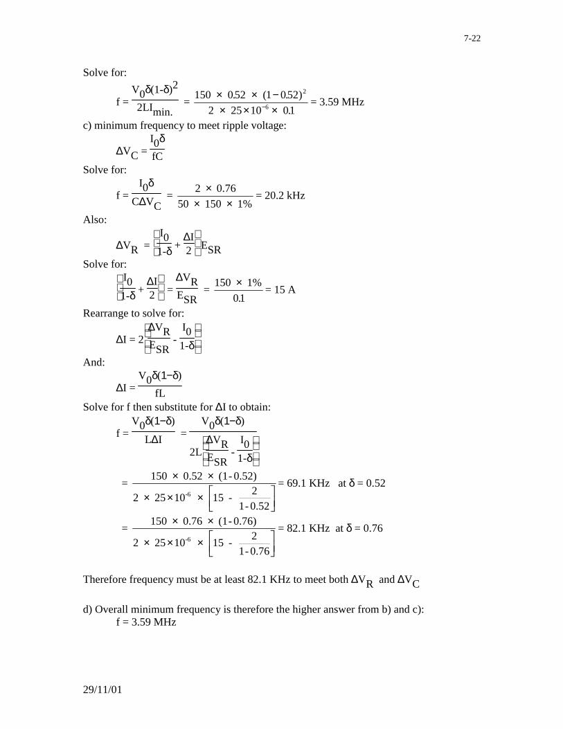
29/11/01
7-22
Solve for:
f = V0δ(1-δ)2
2LImin. =
150 0 52 1 052
2 25 10 01
2
6
× × −× × ×−
. ( . )
.= 3.59 MHz
c) minimum frequency to meet ripple voltage:
∆VC = I0δfC
Solve for:
f = I0δ
C∆VC =
2 0.76
50 150 1%
×× ×
= 20.2 kHz
Also:
∆VR =
I0
1-δ + ∆I2 ESR
Solve for:
I0
1-δ + ∆I2 =
∆VRESR
= 150 1%×
01.= 15 A
Rearrange to solve for:
∆I = 2
∆VR
ESR -
I01-δ
And:
∆I = V0δ(1−δ)
fL
Solve for f then substitute for ∆I to obtain:
f = V0δ(1−δ)
L∆I =
V0δ(1−δ)
2L
∆VR
ESR -
I01-δ
= 150 0.52 (1- 0.52)
2 25 10 15 - 2
1- 0.52-6
× ×
× × ×
= 69.1 KHz at δ = 0.52
= 150 0.76 (1- 0.76)
2 25 10 15 - 2
1- 0.76-6
× ×
× × ×
= 82.1 KHz at δ = 0.76
Therefore frequency must be at least 82.1 KHz to meet both ∆VR and ∆VC
d) Overall minimum frequency is therefore the higher answer from b) and c):
f = 3.59 MHz

29/11/01
7-23
e) The variation in output voltage (in ±%) if the input voltage is 50 V and the transistor "on time" varies by ±1%. At 50V input:
δ = 1 - VSVO
= 1 - 50150 = 0.667
and
VO = VS
(1 - δ) =
50
1( - 0.667 1.01)×= 153.06 V = 150 + 2.05%
= 50
1 0 99( - 0.667 . )×= 147.06 V = 150 - 1.96%
≈ 150 V ± 2%

29/11/01
7-24
7.3 BUCK-BOOST CONVERTER (also known as a Buck-Boost Regulator)
The basic schematic circuit diagram for a Buck-Boost Converter is shown in Figure 7.8.
VL C O
IO
VDV
S
+
-
D
i L
S
(Semiconductor Switch)
RO
Figure 7.8 Basic Schematic Diagram For a Buck-Boost Converter
Switch S is turned on for t1 seconds and then turned off for t2 seconds such
that:
t1 + t2 = Τ (7.3-1)
where Τ is the period for one switching cycle.
We can assume that the output capacitor C is large enough such that Vo is
constant and therefore Io is also constant during the switching period.
When the switch S is turned on at t=0, diode D becomes reverse biased and acts as an open circuit. This is referred to as Mode I and the equivalent circuit for this mode is shown in Figure 7.9.

29/11/01
7-25
VL C O
IO
VS
+
-
i L
S
(Semiconductor Switch)
RO
Figure 7.9 Equivalent Circuit During Mode I
During this mode, the governing equation is:
VL = VS = Li
tL∂
∂ (7.3-2)
Solve for
iL(t) = I1 + VSt
L (7.3-3)
Where I1 is the initial current in inductor L at t=0.
The above equation is valid until the switch S is turned off at t=t1 at which time
the inductor current is defined as I2 , the inductor current at the end of Mode I,
where:
I2 = iL(t1) =I1 + VSt1
L
(7.3-4)
When switch S is turned off, the inductor current continues to flow through the parallel combination of C and RO , and back through diode D. The equivalent
circuit for this mode is shown in Figure 7.10:

29/11/01
7-26
VL C O
IO
D
i L
RO
Figure 7.10 Equivalent Circuit During Mode II
During this mode the governing equation is:
VL = VO = Li
tL∂
∂ (7.3-5)
Solve for;
iL(t) = I2 + VOt
L (7.3-6)
The above equations are valid until the switch turns on again at t=t2 , at which
time the inductor current will be I1 again, assuming steady state conditions,
where;
I1 = iL(t2) = I2 + VOt2
L (7.3-7)
We can obtain two expressions for I2 -I1 :
a) from the end of Mode I, equation (7.3-4) can be rewritten as;
I2 - I1 = VSt1
L (7.3-8)
b) from the end of Mode II, equation (7.3-7) can be rewritten as;

29/11/01
7-27
I2 - I1 = - VOt2
L (7.3-9)
Solve the above equations for
VSt1
L = - VOt2
L (7.3-10)
Define the duty cycle, δ ,as;
δ = t1T (7.3-11)
Where T = t1 + t2 (7.3-12)
∴ t1 = δT (7.3-13)
and t2 = (1-δ)T (7.3-14)
Substitute for t1 and t2 into equation (7.3-10) to obtain:
VS δ = -VO(1-δ) (7.3-15)
The above equation can be simplified to;
VO = -δVS(1-δ)
(7.3-16)
Note that the Buck-Boost is an inverting converter, the output voltage is inverse polarity with respect to the input voltage, and;
Vo < Vs for δ < 0.5 (7.3-17)
Vo > Vs for δ > 0.5 (7.3-18)
Also, define the current swing, ∆I, as:
∆I = I2 -I1 = VSt1
L (7.3-19)
or

29/11/01
7-28
∆I = V0(1−δ)
fL (7.3-20)
where f = 1/T = the switching frequency (7.3-21)
Also, if the capacitor, C, is lossless then the DC current through it will be zero,
and:
I0 = - average (ID ) = (I1 +I2 )(δ-1)/2 (7.3-22)
Solve for
I1 =
I01-δ -
∆I2
I2 = I01-δ +
∆I2
(7.3-23)
Also the capacitor current, iC , can be derived as follows;
iC(t) = - I0 during Mode I (7.3-24)
and iC(t) = - iL(t) - I0 during Mode II (7.3-25)
= - I2 - VOt
L - I0 (7.3-26)
Therefore the peak to peak ripple current in the capacitor can be determined from the above equations:
∆IC = I2 (7.3-27)
or
∆IC = I01-δ +
∆I2 (7.3-28)
Also the peak to peak ripple voltage, ∆VC , can be determined by integrating the
ripple current in the output capacitor;

29/11/01
7-29
∆VC = 1
0Ci (t) tc
t1
∂ (7.3-29)
= 1
0CI to
t1
∂ (7.3-30)
∴ ∆ VC = I0t1C =
I0δfC peak to peak (7.3-31)
Note the above expression for peak to peak ripple does not include "switching spikes" which appear on the output due to high frequency components of the switching waveform which get through the L and C of the output filter.
In particular, the major component of ripple is often due to the equivalent series resistance, ESR , in the output capacitor combined with the ripple current in this
capacitor. This component of output ripple is referred to as ∆VR , where;
∆VR = ∆IC ESR peak to peak (7.3-32)
or
∆VR =
I0
1-δ + ∆I2 ESR (7.3-33)
Usually one of the above, ∆VC or ∆VR , dominates. At high frequencies it’s
∆VR , at low frequencies it’s ∆VC .
Note that in the entire preceding analysis it was assumed that the inductor current, iL , never went to zero.
i.e. I1 > 0 (7.3-34)
Substitute for I1 = I01-δ -
∆I2 > 0 (7.3-35)
or
I1 = I01-δ -
V0(1−δ)
2fL > 0 (7.3-36)

29/11/01
7-30
and solve for;
L > V0(1-δ)2
2fI0 (7.3-37)
This is defined as the critical inductance, LC , where;
LC = V0(1-δ)2
2fI0 (7.3-38)
This gives us the critical, minimum, value for L that will maintain the above equations for ∆I, ∆VC , I1 , I2 and VO .
Conversely, for any given value of L we can solve for the critical, minimum, value of I0 ;
Imin. > V0(1-δ)2
2fL (7.3-39)
This gives us the critical, minimum, value for load on the Buck Converter, I0 , that
will maintain the above equations for ∆I, ∆VC , I1 , I2 and VO .

29/11/01
7-31
Also, for resistive loads;
IO = VORO
= -δVS
RO(1-δ) (7.3-40)
And the output power PO , can be determined;
PO = IO VO = δ2V
2S
RO(1-δ)2 (7.3-41)
For an ideal (lossless) Boost Converter, the input power will be equal to the output power;
Pin = PO (7.3-42)
or;
Iin VS = δ2V
2S
RO(1-δ)2 (7.3-43)
Solve for;
Iin = δ2VS
RO(1-δ)2 = -
δIO(1-δ)
(7.3-44)
Also the input impedance, Rin , can be determined;
Rin = VS /Iin = RO(1-δ)2 /δ2 (7.3-45)
Therefore a boost converter acts like a DC to DC transformer with a
turns ratio of (1 - δ)/δ
.
29/11/01
7-32
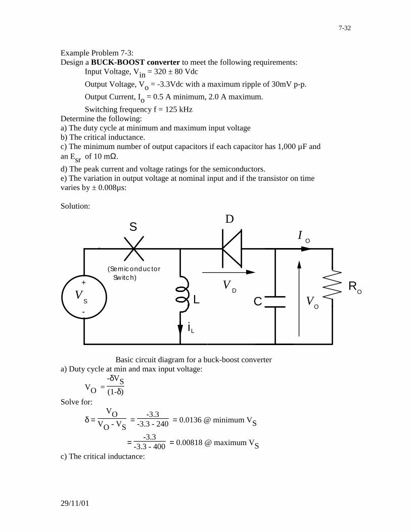
Example Problem 7-3: Design a BUCK-BOOST converter to meet the following requirements: Input Voltage, Vin = 320 ± 80 Vdc
Output Voltage, Vo = -3.3Vdc with a maximum ripple of 30mV p-p.
Output Current, Io = 0.5 A minimum, 2.0 A maximum.
Switching frequency f = 125 kHz Determine the following: a) The duty cycle at minimum and maximum input voltage b) The critical inductance. c) The minimum number of output capacitors if each capacitor has 1,000 µF and an Esr of 10 mΩ.
d) The peak current and voltage ratings for the semiconductors. e) The variation in output voltage at nominal input and if the transistor on time varies by ± 0.008µs: Solution:
VL C O
IO
VDV
S
+
-
D
i L
S
(Semiconductor Switch)
RO
Basic circuit diagram for a buck-boost converter
a) Duty cycle at min and max input voltage:
VO = -δVS(1-δ)
Solve for:
δ = VO
VO - VS =
-3.3-3.3 - 240 = 0.0136 @ minimum VS
= -3.3
-3.3 - 400 = 0.00818 @ maximum VS
c) The critical inductance:

29/11/01
7-33
LC = V 1-
2fIO
O
δ 2
=3.3 (1 - 0.00818)
2 125 10 0.5
2
3
×× × ×
= 26.0 µH
d) The minimum number of output capacitors if each capacitor has 1,000 µF and an Esr of 10 mΩ:
∆VC = IOδfC
Solve for:
C = IOδ
f∆VC =
2 0.0136
125 10 30 103 -3
×× × ×
= 7.25 µF
Therefore one 1,000 µF capacitor would be required if ∆VC were the
determining criteria. Also:
∆VR =
I0
1-δ + ∆I2 ESR
Where:
∆I = VO(1-δ)
fLm
Substitute for ∆I to obtain:
ESR = ∆VR
I0
1-δ + ∆I2
= ∆VR
I0
1-δ + VO(1-δ)
2fLm
= 30 10
2 10
3
3
××
× × × ×
−
−
1 - 0.0136 +
3.32 125 10 26.0 103 -6
= 11.9 mΩ Therefore one 1,000 µF capacitor would be required if ∆VR were the
determining criteria. Therefore the correct number of capacitors is 1. e) The peak current and voltage ratings for the semiconductors:
IQ^ = ID
^ = I01-δ +
∆I2 =
2 10 3
1 - 0.0136 +
3.3
2 125 10 26.0 103 -6
×× × × ×
−
=
2.53 A Peak voltage ratings for the semiconductors:
VQ^ = VD
^ = VS - V0 = 400 - (-3.3) = 403.3 V
e) The variation in output voltage at nominal input and if the transistor on time varies by ± 0.008µs:

29/11/01
7-34
The transistor on time is:
t1 = δf
Where:
δ = VO
VS + VO =
3.3320 + 3.3 = 0.0102 at nominal input
Substitute for δ to obtain:
t1 = δf =
0 0102
125 103
.
×= 0.0817 µs at nominal input
Therefore the variations in t1 , δ and VS will be:
t1 = 0.0817 ± 0.008 µs
δ = t1 f = (0.0817 ± 0.008)×10-6 × 125×103 = 0.0102 ± 0.001
VO = -δVS(1-δ)
= -0.0092 320
(1 - 0.0092)
×= -2.97 V minimum
= -0.0112 320
(1 - 0.0112)
×= -3.62 V maximum
29/11/01
7-35
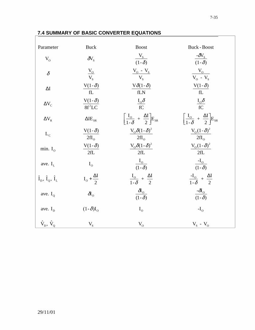
7.4 SUMMARY OF BASIC CONVERTER EQUATIONS
Parameter Buck Boost Buck - Boost
V VV
(1- )
- V
(1- )
V
V
V - V
V
V
V - V
IV(1- )
fL
V (1- )
fLN
V(1- )
fL
VV(1- )
8f LC
I
fC
I
fC
V IEI
- +
I
2E
I
- +
I
2E
LV(1- )
2fI
V (1- )
2fI
V (1- )
2fI
min. IV(1- )
2fL
V (1- )
2fL
V (1-
O SS S
O
S
O S
S
O
O S
C 2O O
R SRO
SRO
SR
CO
O2
O
O2
O
OO
2O
δδ
δδ
δ
δ δ δ δ
δ δ δ
δ δδ δ δ δ
δ δ δ
∆
∆
∆ ∆ ∆ ∆1 1
δ
δ δ
δ δ
δ δδ
δδ
δ
)
2fL
ave. I II
1-
-I
1-
I I I II
2
I
- +
I
2
-I
- +
I
2
ave. I II
1-
- I
1-
ave. I (1- )I I -I
V V V V V - V
2
L OO O
D Q L OO O
Q OO O
D O O O
D Q S O S O
( ) ( )
, ,
( ) ( )
,
+ ∆ ∆ ∆1 1

29/11/01
7-36
Disadvantages of the basic Buck, Boost, and Buck-boost converters: a) Output polarity is fixed with respect to input b) No input/output isolation Input/output isolation is a safety requirement for all AC input power supplies - UL, CSA, EN, IEC requirements. Input/output isolation increases noise immunity and reduces noise emissions. c) Component stresses are maximum Input and output components are subjected to maximum voltage and maximum current, unlike an AC transformer. d) Transient variations in δ result in high transients in output voltage especially severe in converters with high VS /V O ratio
e) Large VS /V O ratio results in very small values for δ and thus maximum
values for LC .
f) Very difficult to get more than one output voltage All of the above problems can be overcome by using a transformer. The simplest way to incorporate a transformer in a DC/DC converter is in a bridge configuration. This can be either a Full Bridge or a Half Bridge.
29/11/01
7-37
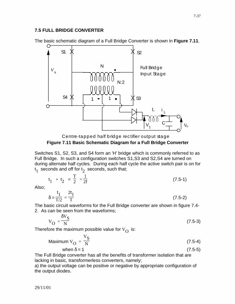
7.5 FULL BRIDGE CONVERTER The basic schematic diagram of a Full Bridge Converter is shown in Figure 7.11.
N:2
N
11
Vo
L
C
Vs
S2S1
S4 S3
i L
V1
Full Bridge Input Stage
Centre-tapped half bridge rectifier output stage Figure 7.11 Basic Schematic Diagram for a Full Bridge Converter
Switches S1, S2, S3, and S4 form an ’H’ bridge which is commonly referred to as Full Bridge. In such a configuration switches S1,S3 and S2,S4 are turned on during alternate half cycles. During each half cycle the active switch pair is on for t1 seconds and off for t2 seconds, such that;
t1 + t2 = T2 =
12f (7.5-1)
Also;
δ = t1
T/2 = 2t1T (7.5-2)
The basic circuit waveforms for the Full Bridge converter are shown in figure 7.4-2. As can be seen from the waveforms;
VO = δVS
N (7.5-3)
Therefore the maximum possible value for VO is:
Maximum VO = VSN (7.5-4)
when δ = 1 (7.5-5) The Full Bridge converter has all the benefits of transformer isolation that are lacking in basic, transformerless converters, namely; a) the output voltage can be positive or negative by appropriate configuration of the output diodes.

29/11/01
7-38
b) the maximum possible output voltage is limited by the turns ratio c) even with extreme variations in δ, the output voltage will never exceed a maximum value determined by N.
d) small VOVS
ratios can be accommodated by small values of N, without
resorting to small values of δ.
e) large VOVS
ratios can be accomodated by large values of N, without
resorting to small values of δ, as would be required with a Buck-Boost converter. f) output components are subjected to VO , IO , stresses only, and input
components are subjected to VS , Iin stresses only, whereas with a
transformerless converter all the components would be subjected to the worst of VO , IO ,VS ,Iin .
g) multiple outputs can be produced by using multiple secondary windings in the transformer and appropriate diode bridges in each output circuit. The basic operation of a full bridge converter is similar to that of a buck converter with two exceptions; a) a transformer with turns ratio N has been inserted between input and output. b) the frequency in the output stage is doubled The net result is that the basic equations for a Full Bridge converter are identical to those of a Buck converter with N inserted appropriately and f changed appropriately.

29/11/01
7-39
Example Problem 7-4: Design a FULL BRIDGE Converter to meet the following requirements: Output voltage: 5 Vdc Output ripple: 50 mV Output capacitor: 125 µF Inductance: 25 µH Peak Diode current: 22 A, Peak Diode Voltage: 50 V Peak Transistor current: 2.2 A, Peak Transistor voltage is undetermined Maximum output current: Io
Minimum output current: 0.1 × Io
Determine: a) Transformer turns ratio for maximum utilization of transistors and diodes. b) Minimum input voltage if maximum duty cycle is 0.95 c) The maximum input voltage and minimum duty cycle. d) Value of Io and ∆I.
e) Maximum Esr for the output capacitor.
f) The minimum frequency if ∆Vc is to be less than 50 mV.
g) The peak transistor voltage. Solution:
N:2
N
11
Vo
L
C
Vs
i L
Basic circuit diagram for a full bridge converter
a) Transformer turns ratio for maximum utilization of transistors and diodes: For maximum utilization of the diodes and transistors the transformer turns ratio should be in the inverse ratio as the current ratings for these semiconductors:
N =
I
ID
Q
= 222.2 = 10
b) Minimum input voltage if maximum duty cycle is 0.95:
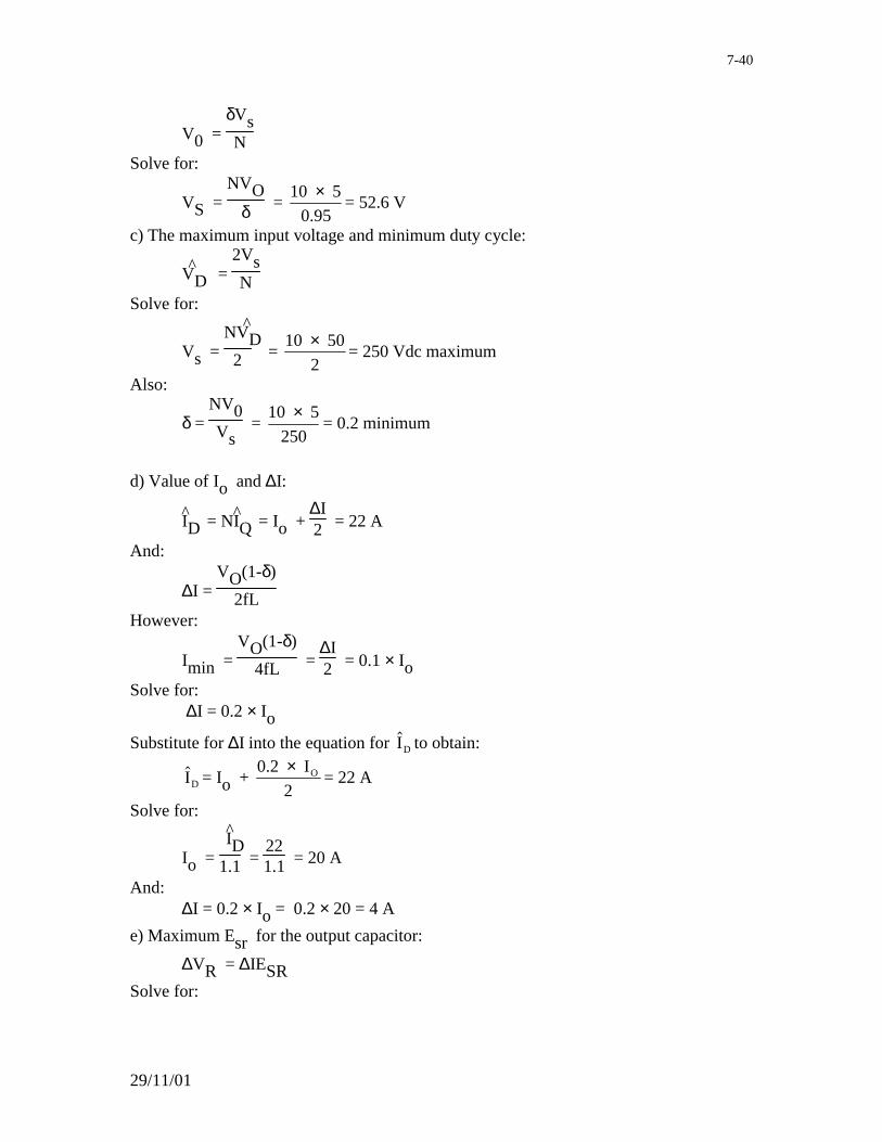
29/11/01
7-40
V0 = δVsN
Solve for:
VS = NVO
δ = 10 5
0.95
×= 52.6 V
c) The maximum input voltage and minimum duty cycle:
VD^ =
2VsN
Solve for:
Vs = NVD
^
2 = 10 50
2
×= 250 Vdc maximum
Also:
δ = NV0Vs
= 10 5
250
×= 0.2 minimum
d) Value of Io and ∆I:
ID^ = NIQ
^ = Io + ∆I2 = 22 A
And:
∆I = VO(1-δ)
2fL
However:
Imin = VO(1-δ)
4fL = ∆I2 = 0.1 × Io
Solve for: ∆I = 0.2 × Io
Substitute for ∆I into the equation for ID to obtain:
ID = Io + 0.2 I
2O×
= 22 A
Solve for:
Io = ID^
1.1 = 221.1 = 20 A
And: ∆I = 0.2 × Io = 0.2 × 20 = 4 A
e) Maximum Esr for the output capacitor:
∆VR = ∆IESR
Solve for:

29/11/01
7-41
ESR = ∆VR∆I
= 504 = 12.5 mΩ
f) The minimum frequency if ∆Vc is to be less than 50 mV:
∆Vc = VO(1-δ)
32f2LC
Solve for:
f = VO(1-δ)
32∆VcLC =
5 (1 - 0.2)
32 50 10 25 10 125 10-3 -6 -6
×× × × × × ×
= 28.3
kHz g) The peak transistor voltage:
VQ^ = Vs = 250 V

29/11/01
7-42
Comparison of equations for Buck and Full Bridge Converters
Parameter
Buck
Converter
Full Bridge
Primary
Full Bridge
Secondary
V VV
N
V
V
NV
V
IV(1- )
fL
V(1- )
2fLN
V(1- )
2fL
VV(1- )
8f LC
V(1- )
32f LC
V IE IE
LV(1- )
2fI
V(1- )
4fI
min. IV(1- )
2fL
V(1- )
4fL
ave. I II
NI
I I II
2
II
2N
II
2
ave. I II
2N
ave. I (1- )II
2
V V V
O SS
O
S
O
S
C 2 2
R SR SR
CO O
O
L OO
O
D Q O
O
O
Q OO
D OO
D Q S
δ δ
δ
δ δ δ
δ δ
δ δ
δ δ
δ δ
δ
−
−
−
−
−
−
++
+
−
−
∆
∆
∆ ∆ ∆
∆∆
∆ ,
, VV
NSS2
29/11/01
7-43
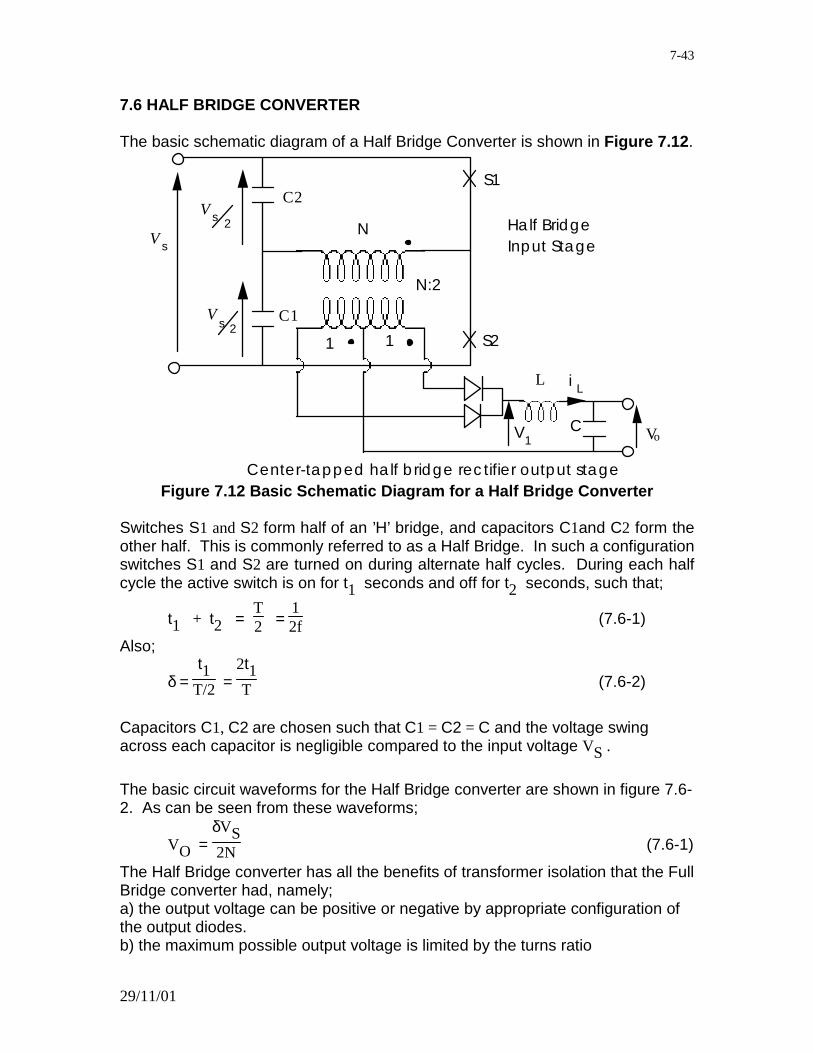
7.6 HALF BRIDGE CONVERTER The basic schematic diagram of a Half Bridge Converter is shown in Figure 7.12.
N:2
N
11
Vo
L
C
Vs
S2
S1
i L
V1
C2
C1
Vs 2
Vs 2
Half Bridge Input Stage
Center-tapped half bridge rectifier output stage Figure 7.12 Basic Schematic Diagram for a Half Bridge Converter
Switches S1 and S2 form half of an ’H’ bridge, and capacitors C1and C2 form the other half. This is commonly referred to as a Half Bridge. In such a configuration switches S1 and S2 are turned on during alternate half cycles. During each half cycle the active switch is on for t1 seconds and off for t2 seconds, such that;
t1 + t2 = T2 =
12f (7.6-1)
Also;
δ = t1
T/2 = 2t1T (7.6-2)
Capacitors C1, C2 are chosen such that C1 = C2 = C and the voltage swing across each capacitor is negligible compared to the input voltage VS .
The basic circuit waveforms for the Half Bridge converter are shown in figure 7.6-2. As can be seen from these waveforms;
VO = δVS2N (7.6-1)
The Half Bridge converter has all the benefits of transformer isolation that the Full Bridge converter had, namely; a) the output voltage can be positive or negative by appropriate configuration of the output diodes. b) the maximum possible output voltage is limited by the turns ratio

29/11/01
7-44
c) even with extreme variations in δ, the output voltage will never exceed a maximum value determined by N.
d) small V
VO
S
ratios can be accommodated by small values of N, without resorting
to small values of δ.
e) large V
VO
S
ratios can be accommodated by large values of N, without
resorting to small values of δ, (as would be required with a Buck-Boost converter. f) output components are subjected to VO , IO , stresses only, and input components are subjected to VS , Iin stresses only, whereas with a transformerless converter all the components would be subjected to the worst of VO , IO , VS , Iin . g) multiple outputs can be produced by using multiple secondary windings in the transformer and appropriate diode bridges in each output circuit. The net result is that the basic equations for a Half Bridge converter are generally identical to those of a Full Bridge converter with VS reduced by 1/2.
The only exception is that the peak transistor voltage, VQ , is the same for both
the half bridge and full bridge converters: VQ = VS for both half bridge and full bridge converters
Half Bridge Converter with AC Input A very common application for Half Bridge converters is in AC to DC power supplies in which the AC input is rectified to produce the VS input voltage to a Half Bridge converter as shown in Figure 7.13.

29/11/01
7-45
N
11
Vo
L
C
S2
S1
i L
V1
C2
C1
Half Bridge Stage
Center-tapped half bridge rectifier output stage
Vsin( ωt)
Voltage Doubler Input Stage
Figure 7.13 Half Bridge Converter With an AC input
Capacitors C1 and C2 are required to filter out the AC ripple in the resultant rectified waveform in order to produce a relatively smooth DC waveform for VS . Thus a half bridge converter is very economical for AC input power supplies because the input capacitors are required anyways for filtering the AC ripple. In the particular case of the voltage doubler circuit shown in Figure 7.13, the capacitors are required not only for filtering but also to produce the voltage double effect. Thus a half bridge converter, when used with AC input power supplies, effectively gets the input capacitors C1 and C2 for "free".

29/11/01
7-46
Example Problem 7-5 You have to design a Half Bridge converter to produce a 5V output using the following components: Output capacitor: C = 6000µF, ESR = 10 mΩ
Inductor: L = 5.5 µH Diode: 150 V, 30 A peak Transistor: 400V, 6 A peak Switching frequency: 200 kHz, Transformer turns ratio 4:1 for input:output. a) Draw the basic circuit diagram, and determine: b) The maximum input voltage and the corresponding duty cycle. c) The minimum input voltage if maximum duty cycle is 0.95. d) The minimum load current. e) The worst case ∆I. Solutions: a) Basic circuit diagram:
N:2
N
11
Vo
L
C
Vs
S2
S1
i L
V1
C2
C1
Vs 2
Vs 2
b) The maximum allowable input voltage and the corresponding duty cycle, if the output voltage is to be 5V:
VQ^ = VS
Therefore:
VS = VQ^ = 400 V
Also:
VD^ =
VSN
Solve for:

29/11/01
7-47
VS = NVD^ = 4 × 150 = 600 V
Therefore the maximum input voltage will be 400 volts limited by the transistor rating. Also:
V0 = δVS2N
Thus the corresponding duty cycle will be:
δ = 2NV0
Vs =
2 4 5
400
× ×= 0.1
c) The minimum input voltage if maximum duty cycle is 0.95:
VS = 2NVO
δ = 2 4 5
0.95
× ×= 42.1 V
d) The minimum load current:
Imin = VO(1-δ)
4fL = 5 (1 - 0.1)
4 200 10 5.5 103 -3
×× × × ×
= 1.03 mA
e) The worst case ∆I:
∆I = VO(1-δ)
2fL = 5 (1 - 0.1)
2 200 10 5.5 103 -3
×× × × ×
= 2.05 mA on secondary side
f) The maximum output current:
ID^ = I0 +
∆I2
Solve for:
I0 = ID^ -
∆I2 = 30 -
0.002052 = 29.999 A = 30 A
Similarly:
IQ^ =
I0N +
∆I2N
Solve for:
I0 = N
IQ^ -
∆I2 = 4 ×
6 -
0.002052 = 24 A
Therefore the maximum output current will be 24 A, limited by the transistor rating. g) The worst case output ripple:
∆Vc = VO(1-δ)
32f2LC =
5 (1 - 0.1)
32 200 10 5.5 10 6000 103 2 -3 -6
×
× × × × × ×= 0.107 µV
Also:
∆VR = ∆IESR = 2.05×10-3 × 10×10-3 = 20.5 µV
Thus the worst case ripple will be 20.5 µV due to ∆VR

29/11/01
7-48
Comparison of Buck and Full Bridge and Half Bridge Converters
Parameter
Buck
Converter
Full Bridge
Converter
Half Bridge
Converter
V VV
N
V
2N
V
V
NV
V
2NV
V
primary IV(1- )
fL
V(1- )
2fLN
V(1- )
2fLN
VV(1- )
8f LC
V(1- )
32f LC
V(1- )
32f LC
V IE IE IE
LV(1- )
2fI
V(1- )
4fI
V(1- )
4fI
min. IV(1- )
2fL
V(1- )
4fL
V(1- )
4fL
ave. I I I I
O SS S
O
S
O
S
O
S
C 2 2 2
R SR SR SR
CO O O
O
L O O O
δ δ δ
δ
δ δ δ
δ δ δ
δ δ δ
δ δ δ
∆
∆
∆ ∆ ∆ ∆

29/11/01
7-49
Comparison of Buck and Full Bridge and Half Bridge Converters (cont’d)
Parameter
Buck
Converter
Full Bridge
Converter
Half Bridge
Converter
I II
2
II
2N
II
2N
I II
2I
I
2I
I
2
ave. I II
2N
I
2N
ave. I (1- )II
2
I
2
V V V V
V V2V
N
V
N
Switches
Diodes 1 2
H.V. Capacitors
Q O
O O
D O O O
Q OO O
D OO O
Q S S S
D SS S
++ +
+ + +
− −
∆∆ ∆
∆ ∆ ∆
δ δ δ
δ
1 4 2
2
2

29/11/01
7-50
7.7 PUSH-PULL CONVERTER
A common type of converter used for low input voltage applications is called a push-pull converter. The basic circuit diagram for such a converter is shown in Figure 7.14.
N
1
1 Vo
L
C
S2
S1
i L
V1
Centre-tapped half bridge rectifier output stage
N
Vs+ -
Vp1
Vp2
Push-Pull Input Stage
Vs1
Vs2
Figure 7.14 Basic Schematic Diagram for a Push-Pull Converter
Switches S1and S2 are turned on during alternate half cycles. During each half cycle the active switch is on for t1 and off for t2 seconds.
Therefore:
t1 + t2 = T2 =
12f (7.7-1)
Also;
δ = t1
T/2 = 2t1T (7.7-2)
Note that the output stage of a push-pull converter is identical to that of a full and/or half bridge converter. Also, a push-pull converter only requires two primary switches and does not require an input capacitor, except for filtering. The operation of a push-pull converter is similar to that of a bridge converter except that when each switch is "on" the complementary "off" switch sees double the input voltage,Vs . The operation of the secondary
side is identical to that of the half bridge and full bridge converters.

29/11/01
7-51
Example Problem 7-6 You have to use a PUSH-PULL Converter that was designed with the following components and constraints: Output capacitor: C = 6000µF, ESR = 10 mΩ
Transformer: N = 4, L = 5.5 mH Diodes: 150 V, 30 A peak Transistors: 400V, 6 A peak Switching frequency: 200 kHz, Duty cycle: 0.8 maximum a) Draw the basic circuit diagram. b) If the output voltage is to be 5V, what would be the maximum allowable input voltage and the corresponding duty cycle. c) What is the minimum input voltage if maximum duty cycle is still 0.8. d) What is the minimum load current. e) What is worst case ∆I. f) What is the maximum output current. g) What is the worst case output ripple. Solution: a) Basic circuit diagram:
N
1
1 Vo
L
C
Q2
Q1
i L
N
Vs+ -
b) If the output voltage is to be 5V, what would be the maximum allowable input voltage and the corresponding duty cycle:
VQ^ = 2VS
Therefore:
VS = VQ^
2 = 4002 = 200 V
VD^ =
2VSN
Solve for:
VS = NVD
^
2 = 4 150
2
×= 300 V
Therefore the maximum input voltage will be 200 volts limited by the transistor rating. Also the corresponding duty cycle will be:
29/11/01
7-52
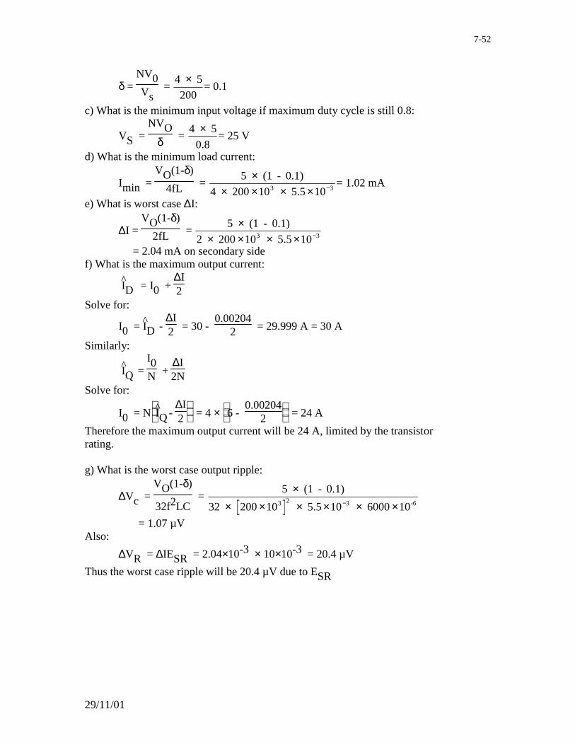
δ = NV0Vs
= 4 5
200
×= 0.1
c) What is the minimum input voltage if maximum duty cycle is still 0.8:
VS = NVO
δ = 4 5
0.8
×= 25 V
d) What is the minimum load current:
Imin = VO(1-δ)
4fL = 5 (1 - 0.1)
4 200 10 5.53
×× × × × −10 3
= 1.02 mA
e) What is worst case ∆I:
∆I = VO(1-δ)
2fL = 5 (1 - 0.1)
2 200 10 5.53
×× × × × −10 3
= 2.04 mA on secondary side f) What is the maximum output current:
ID^ = I0 +
∆I2
Solve for:
I0 = ID^ -
∆I2 = 30 -
0.002042 = 29.999 A = 30 A
Similarly:
IQ^ =
I0N +
∆I2N
Solve for:
I0 = N
IQ^ -
∆I2 = 4 ×
6 -
0.002042 = 24 A
Therefore the maximum output current will be 24 A, limited by the transistor rating. g) What is the worst case output ripple:
∆Vc = VO(1-δ)
32f2LC =
5 (1 - 0.1)
32 200 10 5.5 6000 103 2 -6
×× × × × × ×−10 3
= 1.07 µV Also:
∆VR = ∆IESR = 2.04×10-3 × 10×10-3 = 20.4 µV
Thus the worst case ripple will be 20.4 µV due to ESR

29/11/01
7-53
Comparison of Full Bridge and Push-Pull Converters Full Bridge Converter Push-Pull Converter
Parameter primary secondary primary secondary
VO
δV
SN
δVS
N
∆IV
O(1-δ)
2fLN
VO
(1-δ)
2fL
VO
(1-δ)
2fLN
VO
(1-δ)
2fL
peak VQ
VD
VS
2VS
N 2VS
2VS
N
Switches 4 — 2 —
Diodes — 2 — 2
29/11/01
7-54
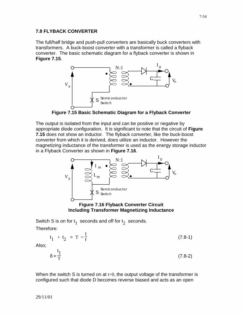
7.8 FLYBACK CONVERTER The full/half bridge and push-pull converters are basically buck converters with transformers. A buck-boost converter with a transformer is called a flyback converter. The basic schematic diagram for a flyback converter is shown in Figure 7.15.
Vs
S
VoC
N:1 I0
Semiconductor Switch
Figure 7.15 Basic Schematic Diagram for a Flyback Converter
The output is isolated from the input and can be positive or negative by appropriate diode configuration. It is significant to note that the circuit of Figure 7.15 does not show an inductor. The flyback converter, like the buck-boost converter from which it is derived, does utilize an inductor. However the magnetizing inductance of the transformer is used as the energy storage inductor in a Flyback Converter as shown in Figure 7.16.
Vs
S
VoC
N:1 I0
Lm
I m
Semiconductor Switch
Figure 7.16 Flyback Converter Circuit
Including Transformer Magnetizing Inductance
Switch S is on for t1 seconds and off for t2 seconds.
Therefore:
t1 + t2 = T = 1f (7.8-1)
Also;
δ = t1T (7.8-2)
When the switch S is turned on at t=0, the output voltage of the transformer is configured such that diode D becomes reverse biased and acts as an open

29/11/01
7-55
circuit. This is referred to a Mode I and the equivalent circuit for this mode is shown in Figure 7.17.
Vs
S
VoC
N:1 I0
Lm
im
Figure 7.17 Equivalent Circuit During Mode I
This equivalent circuit is identical to the Mode I equivalent circuit for a Buck-boost converter as shown in Figure 7.9.
The current, im , through the magnetizing inductance will be the same as the
inductor current in the Buck-boost analysis of Section 7.3:
im(t) = I1 + VSt
L (7.8-3)
When the switch S is opened at t=t1 , the circuit reverts to Mode II. The
equivalent circuit for this mode is shown in Figure 7.18.
VoC
N:1 I0
Lm
i m
i mN
VoC
I0
Lm
N2
a) With Magnetizing inductance on the primary side
b) Magnetizing inductance reflected to the secondary side
i mN

29/11/01
7-56
Figure 7.18 Equivalent Circuit During Mode II
The inductor current at t=t1 is:
im(t1) = I1 + VSt1
L = I2 (7.8-4)
This current cannot go to zero instantaneously and instead it circulates through the transformer as shown in Figure 7.18 and into the output circuit. The diode becomes forward biased and conducts. On the secondary side the magnetizing current becomes, i’m , where:
i’m = Nim (7.8-5)
The equations for a flyback converter in Mode II are similar to those of a buck-boost converter in Mode II except that the output current, voltage and inductance have been reflected through a transformer of turns ratio N.
It is important to note that the flyback converter combines the inductor and transformer into one magnetic device. This is called "integrated magnetics". The flyback converter also provides transformer isolation with only one switch. This is a very economical converter circuit, especially at low power levels (less than 100W). The flyback converter is used in every TV and video monitor to produce the high voltage for CRT deflection.
29/11/01
7-57
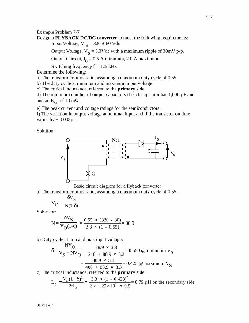
Example Problem 7-7 Design a FLYBACK DC/DC converter to meet the following requirements: Input Voltage, Vin = 320 ± 80 Vdc
Output Voltage, Vo = 3.3Vdc with a maximum ripple of 30mV p-p.
Output Current, Io = 0.5 A minimum, 2.0 A maximum.
Switching frequency f = 125 kHz Determine the following: a) The transformer turns ratio, assuming a maximum duty cycle of 0.55 b) The duty cycle at minimum and maximum input voltage c) The critical inductance, referred to the primary side. d) The minimum number of output capacitors if each capacitor has 1,000 µF and and an Esr of 10 mΩ.
e) The peak current and voltage ratings for the semiconductors. f) The variation in output voltage at nominal input and if the transistor on time varies by ± 0.008µs: Solution:
Vs
Q
VoC
N:1 I0
Basic circuit diagram for a flyback converter
a) The transformer turns ratio, assuming a maximum duty cycle of 0.55:
VO = δVS
N(1-δ)
Solve for:
N = δVS
VO(1-δ) =
0.55 (320 - 80)
3.3 (1 - 0.55)
××
= 88.9
b) Duty cycle at min and max input voltage:
δ = NVO
VS + NVO =
88.9 3.3
240 88.9 3.3
×+ ×
= 0.550 @ minimum VS
= 88.9 3.3
400 88.9 3.3
×+ ×
= 0.423 @ maximum VS
c) The critical inductance, referred to the primary side:
Lc =V (1 )
2fIO
2
O
− δ=
3.3 1 - 0.423
2 125 10 0.53
×× × ×
2
= 8.79 µH on the secondary side

29/11/01
7-58
On the primary side:
Lc = N2 Lc = 88.92 × 8.79×10-6 = 69.4 mH
d) The minimum number of output capacitors if each capacitor has 1,000 µF and an Esr of 10 mΩ:
∆VC = IOδfC
Solve for:
C = IOδ
f∆VC =
2 0.550
125 10 30 103 -3
×× × ×
= 293 µF
Therefore one 1,000 µF capacitor would be required if ∆VC were the
determining criteria. Also:
∆VR =
I0
1-δ + ∆I2 ESR
Where:
∆I = VO(1-δ)
fLm
Substitute for ∆I to obtain:
ESR = ∆VR
I0
1-δ + ∆I2
= ∆VR
I0
1-δ + VO(1-δ)
2fLm
= 30 10
21 - 0.550
+ 3.3 (1 - 0.550)
2 125 10 8.79 10
-3
3 -6
××
× × × ×
=
5.86 mΩ Therefore two 1,000 µF capacitor would be required if ∆VR were the
determining criteria. Therefore the correct number of capacitors is 2. e) The peak current and voltage ratings for the semiconductors:
ID^ =
I01-δ +
∆I2 =
2
1 - 0.550 +
3.3 (1 - 0.550)
2 125 10 8.79 103 -6
×× × × ×
= 5.12 A
IQ^ =
ID^
N = 5.1288.9 = 57.6 mA
Peak voltage ratings for the semiconductors:
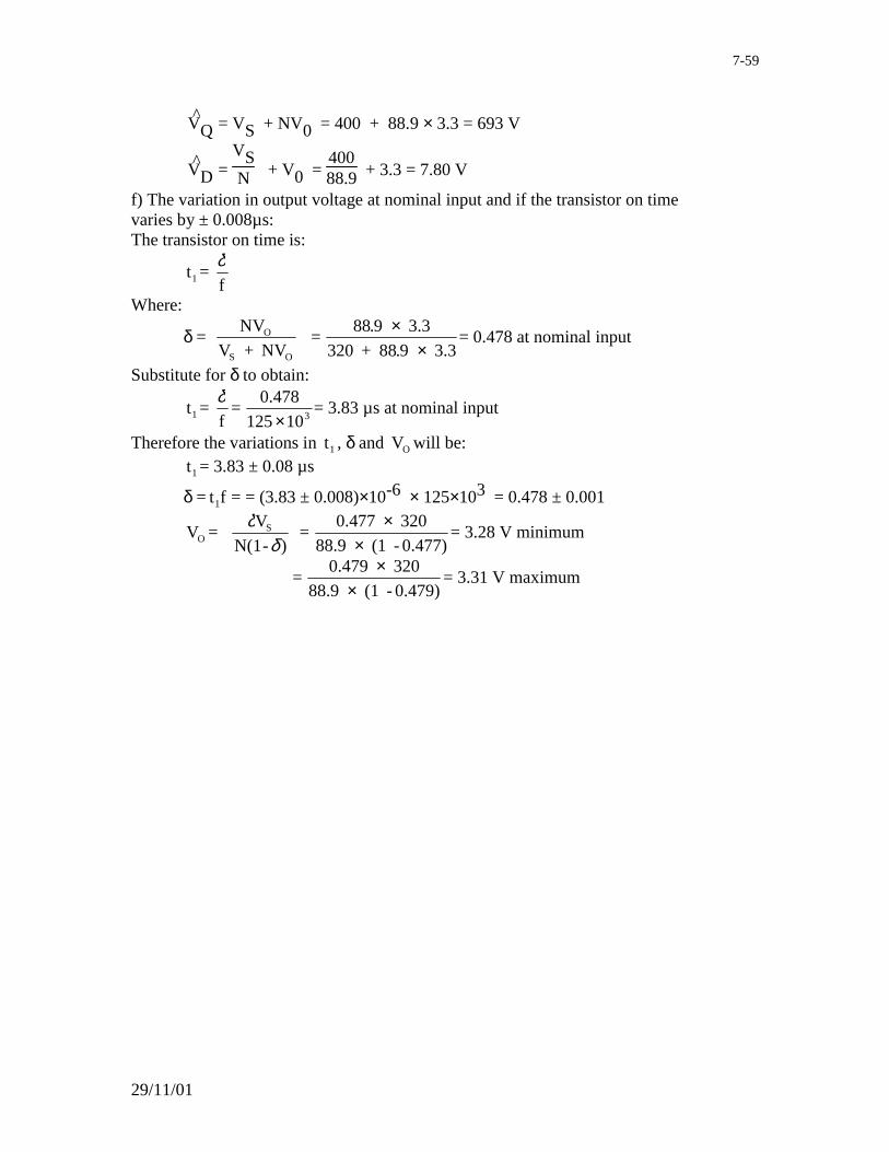
29/11/01
7-59
VQ^ = VS + NV0 = 400 + 88.9 × 3.3 = 693 V
VD^ =
VSN + V0 =
40088.9 + 3.3 = 7.80 V
f) The variation in output voltage at nominal input and if the transistor on time varies by ± 0.008µs: The transistor on time is:
t1 = δf
Where:
δ = NV
V + NV O
S O
= 88 9
88 9
.
.
3.3
320 + 3.3
××
= 0.478 at nominal input
Substitute for δ to obtain:
t1 = δf
= 0.478
125 103×= 3.83 µs at nominal input
Therefore the variations in t1 , δ and VO will be: t1 = 3.83 ± 0.08 µs
δ = t f1 = = (3.83 ± 0.008)×10-6 × 125×103 = 0.478 ± 0.001
VO = V
N(1- ) Sδ
δ=
0.477 320
88.9 (1 - 0.477)
××
= 3.28 V minimum
= 0.479 320
88.9 (1 - 0.479)
××
= 3.31 V maximum

29/11/01
7-60
Comparison of Buck-Boost and Flyback Converters
Buck-Boost Flyback Converter
Error!
average II
1-
I
N(1-
I
1-
II
1- +
I
2
I
N(1- +
I
2
I
1- +
I
2
I , II
1- +
I
2
I
N(1- +
I
2
I
1- +
I
2
V ,V V + V V + NVV
N + V
LO O O
LO O O
Q DO O O
Q D S O S OS
O
δ δ δ
δ δ δ
δ δ δ
)
)
)
∆ ∆ ∆
∆ ∆ ∆
29/11/01
7-61
7.9 PRECAUTIONS WITH SWITCHED MODE POWER SUPPLIES Switched mode power supplies, (also known as SMPS, switchers and SMR’s), have inherent problems which should be appreciated and adressed if they are to be used effectively in any particular application: a) Output Filtering Regardless of how large the output capacitor is or how low its ESR is there will
always be "switching spikes" in the output waveform. These spikes get onto the output due to parasitic capacitances in the output inductor that conduct high frequency components of the switching pulses. These spikes can best be eliminated by using "decoupling" capacitors at the "load" circuitry. b) Input Filtering Many power supplies are sold with little or no input filter capacitors. This can result in high levels of radiated noise and could even damage the power supply (and other circuitry) if the source voltage has significant inductance. c) Heat Switching power supplies are much smaller than "linear" power supplies but they still dissipate heat, often at a much higher volumetric density than linear power supplies. They will overheat if cooling, (air flow), is inadequate. Many so-called high density power supplies are sold on the assumption that an external heat sink and cooling system will be added when in use. d) Ambient Temperature All electronic components and circuits including power supplies have an inherent maximum operating temperature beyond which the circuit will not operate properly and/or components may be damaged. For most power supplies that dissipate a lot of heat the actual operating temperature of the power supply may be significantly higher than the "room ambient". For example a stereo system may operate in a room temperature of 25°C but if the power supply inside it is inadequately cooled its temperature may reach 85°C which is beyond the range of most "commercial grade" components. e) Minimum Load Most switching power supplies have a minimum load requirement that often isn't advertised by the manufacturer. If the power supply is operated below its minimum load the output ripple will be higher than expected and may even cause the power supply to shut down.

29/11/01
7-62
f) Inrush Current If the power supply input filter consists of just a large capacitor then it may draw very high currents everytime input voltage is applied. This may cause fuses and circuit breakers to trip and/or overstress components. Such power supplies may require additional inrush current limiting circuitry. g) Overvoltage Protection This is required to ensure that even if the power supply malfunctions it will still not produce an excessively high output voltage that could damage "downstream" circuitry. The overvoltage protection should be independent of the normal control circuitry. h) Output Current Limit, Current Foldback. This is required to ensure that the power supply does not overheat (and cause fire, or other safety hazards) when the output is overloaded or shorted. Firstly the power supply must survive a permanent overload on its output. Secondly the "downstream" circuitry must be designed such that it too will survive a high current condition. One way to achieve this is to design the power supply such that if there is a short circuit on the output the power supply current "folds back" to a lower and safer value. I) Undervoltage Shutdown This is required to ensure that the power supply doesn’t destroy itself (or cause a fire/shock hazard) if an internal component fails. j) AC Outage and Transient Behaviour If the power supply is fed from commercial AC then it has to be protected against high and low transients and should have graceful shut down in the event of AC failure, with automatic restart when the AC recovers. It is often useful to have "hold-up" capacitors to ride out short duration AC outages, (up to 100 milliseconds). k) Safety All AC input power supplies should be approved by independent safety agencies. In Canada the agency is CSA, (Canadian Standards Association), and in the US it is UL, (Underwriter’s Laboratories). To meet their safety requirements power supplies generally must demonstrate: - input output isolation, typically to 1500V - short circuit protection - internal fault tolerance resulting in no hazard
29/11/01
7-63
- no thermal or electrical overstressing of critical components l) Input Current and Voltage Distortion For many AC input switched mode power supplies the input current is very "peaky" due to the input capacitors which only charge up during a narrow conduction interval during each AC half cycle. This results in: - high rms ripple currents on the input which can lead to overheating of input components - high crest factors, where the crest factor, CF is defined as
CF = I^
Irms Note that for a pure sine wave CF = 1.414
- high levels of third, ninth, fifteenth harmonics which are additive in three phase neutral wires and can result in overheating of the neutral wire - distortion of the input voltage waveform, creating high levels of voltage harmonics which may cause excessive magnetizing losses in other devices connected to the same voltage source The problems associated with input current/voltage distortion can be avoided by "unity power factor" circuits which is usually another power supply in front of the "main" power supply.
29/11/01
7-64
7.10 PROBLEMS 7.10.1 Buck Converters 1. Design a Buck Converter to meet the following requirements; Vs=320±50Vdc, VO =50Vdc,
Maximum ripple=150 mV p-p, IO =5A minimum, 50A maximum,
Switching frequency is 120kHz. Draw the equivalent circuit and determine: a)The minimum duty cycle and under what conditions it occurs. (0.135) b)The minimum inductance required and the worst case average and peak current rating for this inductor. (36µH, 50A average, 55A peak) c)The output capacitance required assuming ESR =0. (69.4ΩF)
d)The output capacitance required assuming ESR =50m
e)The peak voltage and peak current ratings for the semiconductors. (370V, 55A) 2. Design a Buck Converter to operate from a 12V (nominal) car battery. The requirements are; Input Voltage: 10.5 Vdc to 15.9 Vdc Output Current: 0.5A to 1.5A Output Voltage: 5 Vdc Output Ripple: 25mVp-p Switching Frequency: 250kHz Determine; a)The minimum and maximum duty cycle and under what conditions each occurs. (0.314, 0.476) b)The critical inductance. (13.7µH) c)The output capacitance assuming ESR =0. (126µF)
d)The output capacitance assuming ESR =50mΩ/1000µF. (2,000µF)
e)The peak voltage and peak current ratings for the semiconductors. (15.9V, 2.5A)

29/11/01
7-65
7.10.2 Boost Converters 3. You are given a BOOST CONVERTER with the following characteristics: VS = 5 V, VO = 20 V, output C = 100 µF (ESR = 0 ),
∆VC = 250 mV at IO = 1.0 A
Inductor current goes to zero at IO = 0.1 A
Determine: a) The duty cycle, δ. (0.75) b) The switching frequency, f. (30kHz) c) The inductance, L. (156µH)

29/11/01
7-66
7.10.3 Buck-Boost Converters 4. Design a DC/DC Converter to meet the following requirements; Input Voltage, Vs =150±50Vdc,
Output Voltage, Vo =-150Vdc,
Output Current, Io =5A minimum, 50A maximum,
You are given one transistor, one diode, a capacitor of 4700µF, an inductor of 25µH and no transformer. Determine: a)The minimum and maximum duty cycle and under what conditions each occurs. (0.423, 0.600) b)The minimum switching frequency to keep inductor current from going to zero. (196kHz) c)The minimum switching frequency to keep the output ripple within 75 mV p-p. (85.1kHz) d)The peak voltage and peak current ratings for the semiconductors if the switching frequency is 200KHz. (350V, 127.4A)

29/11/01
7-67
7.10.4 Full-Bridge Converters 5. Design a Full Bridge Converter to meet the following requirements; Vs =320±50Vdc,
Vo =50Vdc,
Maximum ripple=150 mV p-p, Io =5A minimum, 50A maximum,
Switching frequency is 120kHz. Determine: a)The transformer turns ration such that the maximum duty cycle does not exceed 95%. (5.13) b)The minimum duty cycle and under what conditions it occurs. (0.69) c)The minimum inductance required and the worst case average and peak current rating for this inductor. (6.46µH, 50A average, 55A peak) d)The output capacitance required assuming ESR =0. (34.7µF)
e)The output capacitance required assuming ESR =50mΩ/1000µF. (4,000µF)
f)The peak voltage and peak current ratings for the semiconductors. (370V, 10.7A, 144V, 55A) 6. Design a Full Bridge Converter to meet the following requirements; Vs =300±50Vdc,
Vo =50Vdc,
Maximum ripple=200 mV p-p, Io =1A minimum, 25A maximum,
Switching frequency is 200kHz. Determine: a)The transformer turns ration such that the maximum duty cycle does not exceed 99%. (4.95) b)The minimum duty cycle and under what conditions it occurs. (0.707) c)The minimum inductance required and the worst case average and peak current rating for this inductor. (18.3µH, 25A average, 26A peak) d)The output capacitance required assuming ESR =0. (3.13µF)
e)The output capacitance required assuming ESR =8mΩ/1000µF. (1000µF)
f)The peak voltage and peak current ratings for the semiconductors. (350V, 5.25A, 141V, 26A)

29/11/01
7-68
7. Design a Full Bridge DC-DC converter to meet the following requirements: Input Voltage, Vs =150Vdc ± 50Vdc
Output Voltage, Vo = 5Vdc with a maximum ripple of 150mV p-p.
Output Current, Io = 10A minimum, 100A maximum.
Switching frequency is 200kHz. Determine the following: a) The transformer turns ratio. (20) b) The duty cycle during minimum, nominal, and maximum input voltage. (1.0, 0.667, 0.5) c) The critical inductance. (0.3125µH) d) The peak input current, using the inductance value determined in part c). (5.5A) e) The output capacitance assuming no ESR . (41.7µF)
f) The output capacitance assuming capacitors are available in cans of 1000 uF and 15 milliohms ESR in each can. (2000µF)
8. Design a 500Vdc, 10KW power supply for a resistive load using a transformer and four transistors in a Full Bridge configuration. The input voltage varies from 176 to 265 Vdc. The switching frequency must be 50kHz, and the minimum load is 200W. The output ripple is to be 6Vp-p. Determine: a)The transformer turns ratio, assuming the maximum duty cycle must not exceed 95%. (0.334) b)The minimum duty cycle. (0.631) c)The critical inductance. (2.31µH) d)The output capacitance assuming ESR =0. (166µF)
e)The output capacitance assuming capacitors are available in 100µF cans, each with ESR =1Ω. (100µF)
f)The peak voltage and peak current ratings for the semiconductors. (265V, 61.1A, 1587V, 20.4A) 9. Design a Full Bridge DC-DC converter to meet the following requirements: Input Voltage, Vs =50Vdc ± 10Vdc
Output Voltage, Vo = 5Vdc with a maximum ripple of 150mV p-p.
Output Current, Io = 30A minimum, 120A maximum.
Switching frequency is 40kHz. Determine the following: a) The transformer turns ratio. (8) b) The duty cycle during minimum, nominal, and maximum input voltage. (1.0, 0.8, 0.67) c) The critical inductance. (0.347µH) d) The output capacitance assuming no ESR . (625µF)
e) The output capacitance assuming capacitors are available in
29/11/01
7-69
cans of 1000 µF and 15 milliohms ESR in each can. (6000µF)
f)The peak voltage and peak current ratings for the semiconductors. (60V, 18.75A, 15V, 150A) 7.10.5 Half Bridge Converters 10. Design a Half Bridge Converter to meet the following requirements; VS =300±50Vdc,
V0 =50Vdc,
Maximum ripple=200 mV p-p, I0 =1A minimum, 25A maximum,
Switching frequency is 200kHz. Determine: a)The transformer turns ration such that the maximum duty cycle does not exceed 99%. (2.475) b)The minimum duty cycle and under what conditions it occurs. (0.707) c)The minimum inductance required and the worst case average and peak current rating for this inductor. (18.3µH, 25A average, 26A peak) d)The output capacitance required assuming ESR =0. (3.13µF)
e)The output capacitance required assuming capacitors are available in 1000µF cans each with ESR =8mΩ. (1000µF)
f)The peak voltage and peak current ratings for the semiconductors. (350V, 10.5A, 141V, 26A)

29/11/01
7-70
7.10.6 Push-Pull Converters 11. Design a Push-Pull Converter to meet the following requirements; VS =320±50Vdc,
V0 =50Vdc,
Maximum ripple=150 mV p-p, I0 =5A minimum, 50A maximum,
Switching frequency is 120kHz. Determine: a)The transformer turns ration such that the maximum duty cycle does not exceed 95%. (5.13) b)The minimum duty cycle and under what conditions it occurs. (0.69) c)The minimum inductance required and the worst case average and peak current rating for this inductor. (6.46µH, 50A average, 55A peak) d)The output capacitance required assuming ESR =0. (34.7µF)
e)The output capacitance required assuming ESR =50mΩ/1000µF. (4,000µF)
f)The peak voltage and peak current ratings for the semiconductors. (740V, 10.7A, 144V, 55A) 12. Design a Push-Pull Converter to meet the following requirements; VS =300±50Vdc,
V0 =50Vdc,
Maximum ripple=200 mV p-p, I0 =1A minimum, 25A maximum,
Switching frequency is 200kHz. Determine: a)The transformer turns ration such that the maximum duty cycle does not exceed 99%. (4.95) b)The minimum duty cycle and under what conditions it occurs. (0.707) c)The minimum inductance required and the worst case average and peak current rating for this inductor. (18.3µH, 25A average, 26A peak) d)The output capacitance required assuming ESR =0. (3.13µF)
e)The output capacitance required assuming capacitors are available in 1000µF cans, each with ESR =8mΩ. (1000µF)
f)The peak voltage and peak current ratings for the semiconductors. (700V, 5.25A, 141V, 26A)

29/11/01
7-71
7.10.7 Flyback Converters 13. Design a Flyback Converter to meet the following requirements; VS =320±50Vdc,
V0 =50Vdc,
Maximum ripple=150 mV p-p, I0 =5A minimum, 50A maximum,
Switching frequency is 120kHz. Determine: a)The transformer turns ration such that the duty cycle is 50% at nominal input voltage. (6.4) b)The minimum and maximum duty cycle and under what conditions each occurs. (0.464, 0.533) c)The minimum inductance required (referred to the primary) and the worst case average and peak current rating for this inductor. (490µF, 9.2A average, 19.56A peak) d)The output capacitance required assuming ESR =0. (1506µF)
e)The output capacitance required assuming capacitors are available in 1000µF cans each with ESR =50mΩ. (37,000µF)
f)The peak voltage and peak current ratings for the semiconductors. (690V, 19.56A, 107.8V, 125.2A) 14. Design a Flyback Converter to meet the following requirements; VS =300±50Vdc,
V0 =50Vdc,
Maximum ripple=200 mV p-p, I0 =1A minimum, 25A maximum,
Switching frequency is 200kHz. Determine: a)The transformer turns ration such that the duty cycle is 50% at nominal input voltage. (6) b)The minimum and maximum duty cycle. (0.462, 0.545) c)The minimum inductance required (referred to the secondary) and the worst case average and peak current rating for this inductor. (36.2µH, 54.95A average, 56.5A peak) d)The output capacitance required assuming ESR =0. (340.6µF)
e)The output capacitance required assuming ESR =8mΩ/1000µF. (2000µF)
f)The peak voltage and peak current ratings for the semiconductors. (650V, 9.42A, 108V, 56.5A)

29/11/01
7-72
15. Design a flyback converter to meet the following requirements: Input Voltage, VS = 300 V
Output Voltage, V0 = 20 Vdc, maximum ripple of 250 mV p-p
Output Current, I0 = 1.0 A
Duty cycle = 0.5 Switching frequency = 500 kHz Determine the following: a) The transformer turns ratio. (15) b) The critical transformer magnetizing inductance referred to the primary. (1125µH) c) The output capacitance assuming no ESR . (4µF)
e) The output capacitance assuming capacitors come in cans of100 µF and 500 milliohms ESR in each can. (800µF)
16. Design a 500Vdc, 100W power supply for a resistive load using Flyback Converter. The input voltage is 312 Vdc ±15%. The switching frequency must be 150kHz, and the minimum load is 20W. The output ripple is 6Vp-p. Determine: a)The transformer turns ratio, assuming the duty cycle must 50% at nominal input and maximum output. (0.624) b)The minimum and maximum duty cycle. (0.465, 0.541) c)The critical magnetizing inductance, referred to the primary. (4.64mH) d)The output capacitance assuming ESR =0. (120µF)
e)The peak voltage and peak current ratings for the semiconductors. (671V, 0.8A,1075V, 0.5A) 17. Design a Fyback Converter to meet the following requirements; Output Voltage, Vo =150Vdc,
Output Current, Io =5A minimum, 50A maximum,
You are given a capacitor of 470µF, and a transformer with a turns ratio of 2:1, a magnetizing inductance of 100 µH on the input side, (25µH on the output side. Determine: a)The input voltage range for 0.4 < δ < 0.6. (200V to 450V) b)The minimum switching frequency to keep inductor current from going to zero. (216kHz) c)The minimum switching frequency to keep the output ripple within 75 mV p-p. (851kHz) d)The peak voltage and peak current ratings for the semiconductors if the switching frequency is 200kHz. (750V, 65.5A, 375V, 131A)
Related Documents