CHAPTER SIX Theoretical Advances in the Electronic and Atomic Structures of Silicon Nanotubes and Nanowires Abhishek Kumar Singh, 1,2 Vijay Kumar 3,4,5 and Yoshiyuki Kawazoe 2 Contents 6.1 Introduction 218 6.2 Computational Approach 220 6.3 Silicon Nanotubes 220 6.3.1 Metal Encapsulated Nanotubes of Silicon 222 6.3.2 Electronic Structure and Bonding Nature 225 6.3.3 Magnetism in Metal Encapsulated SiNTs 228 6.4 Germanium Nanotubes 231 6.4.1 Metallic and Semiconducting Nanotubes of Ge 233 6.5 Silicon Nanowires 235 6.5.1 Non-Crystalline Pristine SiNWs 237 6.5.2 Crystalline Pristine SiNWs 238 6.5.3 Band Structure of SiNWs 243 6.6 Hydrogenated Nanowires 244 6.6.1 Electronic Structure of Hydrogenated SiNWs 249 6.6.2 Effects of Doping and H Defects 251 6.7 Nanowire Superlattices 253 6.8 Conclusion and Perspective Remarks 254 Acknowledgements 255 References 255 Abstract Nanotubular and nanowire structures of silicon are currently of great interest for miniature devices. Recently, using cluster assembly approach, nanotubular forms of silicon have been shown to be stabilized by encapsulation of metal atoms. Here we review these develop- ments and discuss the stability of such nanostructures and their electronic properties 1 Materials Department, University of California Santa Barbara, Santa Barbara, CA, USA. 2 Institute for Materials Research, Tohoku University,Aoba-ku, Sendai, Japan. 3 Dr. Vijay Kumar Foundation, 45 Bazaar Street, K. K. Nagar (West), Chennai, India. 4 The Institute of Mathematical Sciences, Taramani, Chennai, India. 5 Research Institute for Computational Sciences (RICS), National Institute of Advanced Industrial Science and Technology (AIST),AIST Tsukuba Central 2, Umezono, Tsukuba, Japan. Nanosilicon Copyright © 2007. Elsevier Ltd. 9780080445281 All rights reserved.

Welcome message from author
This document is posted to help you gain knowledge. Please leave a comment to let me know what you think about it! Share it to your friends and learn new things together.
Transcript
C H A P T E R S I X
Theoretical Advances in theElectronic and Atomic Structures ofSilicon Nanotubes and Nanowires
Abhishek Kumar Singh,1,2 Vijay Kumar3,4,5 and Yoshiyuki Kawazoe2
Contents6.1 Introduction 2186.2 Computational Approach 2206.3 Silicon Nanotubes 220
6.3.1 Metal Encapsulated Nanotubes of Silicon 2226.3.2 Electronic Structure and Bonding Nature 2256.3.3 Magnetism in Metal Encapsulated SiNTs 228
6.4 Germanium Nanotubes 2316.4.1 Metallic and Semiconducting Nanotubes of Ge 233
6.5 Silicon Nanowires 2356.5.1 Non-Crystalline Pristine SiNWs 2376.5.2 Crystalline Pristine SiNWs 2386.5.3 Band Structure of SiNWs 243
6.6 Hydrogenated Nanowires 2446.6.1 Electronic Structure of Hydrogenated SiNWs 2496.6.2 Effects of Doping and H Defects 251
6.7 Nanowire Superlattices 2536.8 Conclusion and Perspective Remarks 254Acknowledgements 255References 255
AbstractNanotubular and nanowire structures of silicon are currently of great interest for miniaturedevices. Recently, using cluster assembly approach, nanotubular forms of silicon have beenshown to be stabilized by encapsulation of metal atoms. Here we review these develop-ments and discuss the stability of such nanostructures and their electronic properties
1Materials Department, University of California Santa Barbara, Santa Barbara, CA, USA.2Institute for Materials Research, Tohoku University,Aoba-ku, Sendai, Japan.3Dr. Vijay Kumar Foundation, 45 Bazaar Street, K. K. Nagar (West), Chennai, India.4The Institute of Mathematical Sciences, Taramani, Chennai, India.5Research Institute for Computational Sciences (RICS), National Institute of Advanced Industrial Science andTechnology (AIST),AIST Tsukuba Central 2, Umezono, Tsukuba, Japan.
Nanosilicon Copyright © 2007. Elsevier Ltd.9780080445281 All rights reserved.
including metallic, semiconducting, and magnetic behaviours. Hydrogenated and oxy-genated structures of silicon can also be made in tubular forms. These could be amongthe thinnest semiconducting nanostructures of silicon. Thicker quasi-one-dimensionalstructures of silicon have been grown in the form of nanowires which could be metallic orsemiconducting. We discuss surface reconstruction in such nanowires and their electronicproperties. Further effects of p- or n-type doping as well as hydrogen defects on the atomicand electronic structures of hydrogenated Si nanowires are presented. The metallic, semi-conducting, and optical properties of silicon in such nanostructures could make it pos-sible to develop novel silicon-based nanodevices.
6.1 Introduction
Nanoforms of silicon hold great promise for nanotechnology as bulk siliconhas been for microelectronics. Silicon acquires a much desired advantage at thenanoscale that it could be luminescent in the visible range. In 1991, an importantbreakthrough happened when photoluminescence was discovered from porous sil-icon [1]. It was thought to be due to the formation of quasi-one-dimensional struc-tures or the presence of nanoparticles. Since then much progress has been made inthe understanding of the properties of nanoparticles and quasi-one-dimensionalstructures of silicon such as nanotubes and nanowires and new opportunities haveopened up for novel applications in nanodevices. In recent years it has become pos-sible to synthesize silicon nanowires (SiNWs) as well as nanoparticles with a con-trol on size and several potentially important applications have been demonstratedin laboratory. The finding of bright luminescence in nanoforms of silicon in contrastto bulk, which is a bad emitter of light, could help in achieving a long standing goalof the integration of optoelectronic with microelectronics and this could offer entirelynew applications of silicon.
Another strong reason for the intense research on nanoforms of silicon is that in thetop-down approach it is perceived that the continuously shrinking size of the silicon-based device components will hit a road block due to the chemical and the physicallimitations. Therefore, much research is being done to find alternate device compon-ents for future technologies. In the bottom-up approach, nanoparticles and quasi-one-dimensional structures of silicon, molecular electronics, and carbon nanotubeshave been attracting much attention. The mechanical stability as well as ballistic trans-port properties of carbon nanotubes [2] are attractive and several possibilities of theirapplications [3–10] have been explored over the past decade. There is,however,a prob-lem from the point of view of devices in that nanotubes of different diameters and chir-ality often coexist. As nanotubes with different chirality could be semiconducting ormetallic, it is important to separate them for device applications and it is still a big prob-lem for commercial application. On the other hand conventional silicon-based devicefabrication technology is so well established that only overwhelmingly compellingnew technology will be able to replace it. Therefore, continuous efforts are going onfor understanding the properties of nanoforms of silicon as well as the miniaturizationof silicon devices since they could prove to be more convenient and economical forcommercialization than any other process as much is known about silicon and it couldbe possible to take advantage of the existing infrastructure. One such example is that
218 Abhishek Kumar Singh, Vijay Kumar and Yoshiyuki Kawazoe
of a single electron transistor (SET) memory made up of silicon [11,12], whose fabri-cation process relies only on the technology already developed for MOSFETs (seeChapter Ten).
History of the SiNWs goes back to the finding of luminescence from porous silicon. Quasi-one-dimensional structures in the form of square or rectangularSiNWs were studied to understand the effects of quantum confinement [13–20].These SiNWs were shown to have direct band gap which is important for lumines-cence. Progress has been more rapid in recent years and currently, it has become pos-sible to produce SiNWs with a control on size and growth direction [21–26]. Thesedevelopments have stimulated much theoretical and experimental research. Effortsare being made to develop a fundamental understanding of the electronic, optical,magnetic, thermal, and mechanical properties of such materials and their dependenceon size and morphology as well as the changes due to interaction with other species.As a large fraction of atoms in a nanowire lies on the surface, the extensive know-ledge available on the atomic and electronic structures of the surfaces of bulk siliconoffers an advantage to understand the surface properties of SiNWs and to fabricatefunctional devices. Doping of SiNWs by boron and phosphorus has been achieved todevelop [27,28] p- and n-type elements for active devices, and even integration ofsuch devices to perform some of the basic computations [29] has been demonstrated(see Chapter 5). SiNWs are biocompatible and their potential for biological as well aschemical sensors even at the molecular scale has been demonstrated [30–35]. Boron-doped SiNWs have been shown [30] to be highly sensitive and selective nanosensorsfor biological and chemical species. SiNWs functionalized with amines and an oxidelayer exhibit pH-dependent conductance due to the change in the surface chargeduring protonation and deprotonation. Biotin-modified SiNWs are used to detectstreptavidin down to at least a picometer concentration range. Antigen functionalizedSiNWs show reversible antibody binding and concentration-dependent detection inreal time. The details of these developments are covered in Chapter Five.
Besides SiNWs,nanotubes are the other structures in quasi-one-dimensional formand several theoretical studies have been made on the stability of tubular forms of sil-icon similar to the carbon nanotubes [36–39]. It has been found that diamond-likenanowire structures are more favourable for silicon than nanotubes. There are experi-mental reports of tubular form of silicon where nanotubes [40–42] are formed witha very thick tube wall. However, these have not yet been well understood. A novelnanoform of silicon has recently emerged where metal encapsulation is used to real-ize silicon fullerenes [43–52] and nanotubes [53–56]. These are more stable thannanostructures formed from elemental silicon, have high symmetries, and potentialfor mass production with size selection. Their electrical, magnetic, and optical prop-erties [57] can be changed by changing the metal atoms. Metal encapsulated siliconclusters could be assembled to form new varieties of silicon. Many different promis-ing properties such as metallic behaviour [53], magnetism [54], vibrational, andoptical properties have been found. The details have been covered by Kumar in aseparate chapter. Here we shall discuss the assembly of metal encapsulated clustersthat led to the discovery of metal encapsulated silicon nanotubes (SiNTs).
There are several important factors that differentiate nanoforms of a material fromthe corresponding bulk phases. The large fraction of atoms lying on the surface of ananomaterial could lead to atomic structures that are different from bulk. A quantitative
Electronic and Atomic Structures of SiNTs and SiNWs 219
understanding of these from experiments is difficult. For SiNWs, the presence of edgeswhere two facets meet could lead to new reconstructions that are not known on flatbulk surfaces while thin SiNWs and SiNTs may have completely new structures. Thedangling bonds on the surface could lead to states within the band gap and may dra-matically affect the optical properties. For nanostructures with lateral dimensions ofthe order of the carrier de Broglie wavelength,quantum confinement could affect thegap energies leading to the possibility of visible photoluminescence and thereforenew applications of silicon. The properties of such structures and their applicationsrely heavily on the electronic structure. Therefore, for the rapid development of thisfield, advances in the understanding of the atomic and electronic structures of SiNWsand SiNTs as well as the various possible ways to modify these are very important.Computer simulations can play a very important role in understanding the propertiesand phenomena under controlled conditions. It is also important that such calcula-tions are performed using tools that have predictive capabilities. Here we review suchtheoretical developments on quasi-one-dimensional structures of silicon that arecurrently attracting much attention (see also Chapter Eight). A brief summary of thecomputational approaches that have been employed for the study of these system isgiven in the next section.
6.2 Computational approach
Theoretical results presented in this chapter have been mostly obtained usingab initio electronic structure calculations based on the solution of the Kohn–Shamequations within the density functional theory (DFT) [58]. DFT has been enor-mously successful using the local density approximation (LDA) and by taking intoaccount gradient corrections within the generalized gradient approximation (GGA)[59] which often improves the LDA results by correcting the overbinding. Althoughdifferent ways exist to solve the Kohn–Sham equations, a plane wave basis approachusing pseudopotentials [60,61] is quite efficient for understanding the chemical bond-ing and associated properties of such systems. It seems to be most advantageous par-ticularly in cases where ion dynamics needs to be performed and this is often the casefor nanomaterials. The basis set is complete and the calculations can be performedon an equal footing for a variety of systems such as molecules, nanotubes, nanowires,quantum dots, perfect crystals, defects, and surfaces. Therefore, this method providesa possibility to understand the evolution of the properties of matter from atomic andmolecular levels to the bulk phase with the same level of accuracy. Results obtainedby such methods often agree with experiments closely and in some cases even pre-dictions have received subsequent experimental support. Such simulations can be veryadvantageous in exploring different possibilities and to design new materials evenbefore experiments are done.
6.3 Silicon nanotubes
The discovery of carbon nanotubes led to the curiosity if similar structures ofsilicon could be formed. However, unlike carbon, which can form sp, sp2, and sp3
220 Abhishek Kumar Singh, Vijay Kumar and Yoshiyuki Kawazoe
bonded structures, silicon prefers predominantly sp3 bonding and does not exist in sp2
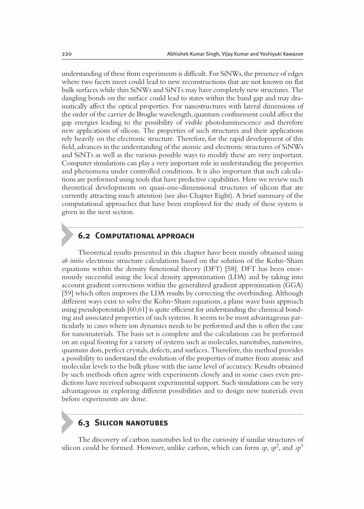
bonded form by itself. Puckered layers exist in AlB2 type compound Ca(AlxSi1�x)2 orSr(Ga,Si)2 and this has been considered to be a possible system that could lead to theformation of nanotubes [62,63] (see Fig. 6.1). Seifert et al. have studied [62] the sta-bility of such a nanotube by folding a puckered sheet. In these compounds largecharge transfer takes place between Ca and Al/Si atoms and therefore Si atoms are inapproximately Si�configuration. The stability of such a charged hypothetical SiNTwas studied by using a tight binding method and it was found to be stable [63]. In Si�
configuration, a Si atom can be replaced by a P atom and nanotubes of P with simi-lar structure have also been found to be stable [64]. In another approach the danglingbonds in such a nanotube have been saturated by H atoms to form a nanotube ofSi!H. Due to the puckered nature H atoms are on both the sides of a nanotube.A graphite type layer of Si with H atoms on one side is found to be unstable. However,small nanotubes with dangling bonds on the outer side passivated by H atoms arestable because the bonding in small nanotubes becomes more sp3 type.
There are reports of the stability of (n,m) type SiNTs with hexagonal atomic struc-tures similar to those of carbon nanotubes. However, a comparative study [65] of thehexagonal and puckered SiNTs showed puckered nanotubes to be more stable and itsupports the preference for sp3 bonding in tubular structures of silicon. The (n,n)SiNTs (n � 5–11) were found to be semiconducting. The band gap decreases with anincrease in diameter. On the other hand (n,0) SiNTs (n � 10–24) are semiconducting
Electronic and Atomic Structures of SiNTs and SiNWs 221
Si backbone
Bundle I
a2
c Si0 c0.5 c
Ca0 c
0.5 ca1
Bundle II
Tube A Tube B Tube C
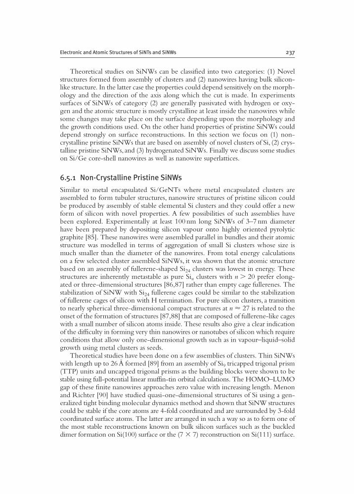
Figure 6.1 Schematic drawing of the cross-sections of nanotubes with different possibilities toaccommodate 12 Ca atoms of the CaSi2 in (6,6) tube.The bright Si and Ca atoms are located at0 c and the dark ones at 0.5 c along the c-axis.The different packing schemes investigated in thisstudy are also depicted in the lower part of the figure (Reproduced with permission from Ref.[63] copyright APS 2003).
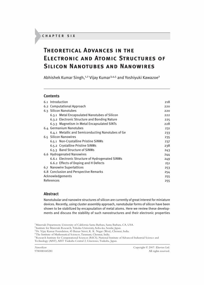
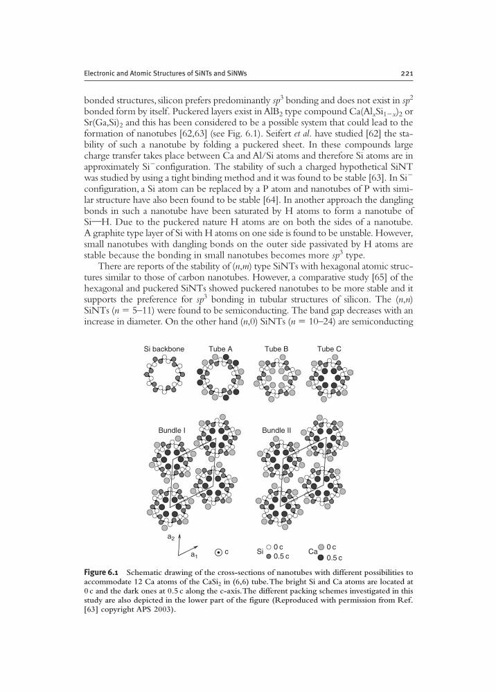
but the band gap decreases in a period of 3. The (n,0) SiNTs with n � 5–9 are metal-lic as for small diameter nanotubes the mixing of σ* and π* states is strong. Faganet al. [37] showed that the strain energy to fold a hexagonal sheet of Si into a nan-otube is about 0.04 eV/atom which is similar to the value of carbon nanotubes.However, a graphene-like sheet of Si has 0.83 eV/atom lower binding energy (BE)as compared to the diamond structure and this makes the stabilization of agraphene-like sheet of Si difficult. The cohesive energy of a hexagonal nanotubes ofSi is about 82% of the bulk value while for carbon nanotubes it is around 99%.There are reports [66] of the production of self-assembled SiNTs from a powder ofsilicon monoxide under supercritical hydrothermal condition with a temperature of470°C and a pressure of 6.8 MPa. These multiwalled nanotubes have closed capswith a pore inside and 0.31 nm interplanar spacing. On the outer side there are2–3 nm thick amorphous layers of SiO2. SiNTs have also been grown [40] on a reg-ular array of hexagonal porous alumina by molecular beam epitaxy (see Fig. 6.2). Theouter layers of such nanotubes are also covered with an oxide layer.
An alternative approach to stabilize sp2 bonding in silicon and to form nanotubescould be by doping Si with metal atoms. As briefly mentioned above, metal encapsu-lation has led to novel fullerene-like and other polyhedral clusters of silicon and ger-manium [67]. Assembly of metal encapsulated clusters has been shown [68] to lead tothe formation of silicon and germanium nanotubes. The properties of such nanotubesare controlled by the metal atoms and it has been possible to develop metallic, semi-conducting, and magnetic nanotubes. In the following we discuss these developments.
6.3.1 Metal Encapsulated Nanotubes of Silicon
Silicon has 6-membered rings in the bulk diamond structure. In an effort to developquasi-one-dimensional structures of Si, stacking of such 6-membered chair-shapedunits was considered [53]. The optimized structures of such assemblies (Fig. 6.3) were
222 Abhishek Kumar Singh, Vijay Kumar and Yoshiyuki Kawazoe
(a) (b)
100 nm 100 nm
Figure 6.2 (a) Typical transmission electron microscope images (TEM) of the SiNTs.The darkand bright areas indicate Si and SiO2 layers, respectively. The wall thickness of the SiNTs are4–5nm, shown in left inset.The dotted circle marked the tip morphology of the SiNTs. Insetleft: High-magnification image of the SiNTs; right: the selected area electron diffraction pat-tern (SAED) rings taken from the SiNTs. (b) TEM image of SiNTs after HF treatment. Insetleft: HRTEM image reveals that lattice fringe of the silicon wall is about 1.91Å; right: theSAED pattern spot taken from the SiNTs (Reproduced with permission from Ref. [40]).
Electronic and Atomic Structures of SiNTs and SiNWs 223
(a) (b) (c)
(e) (f) (g)Group I
Group III
Group II
(d)
�
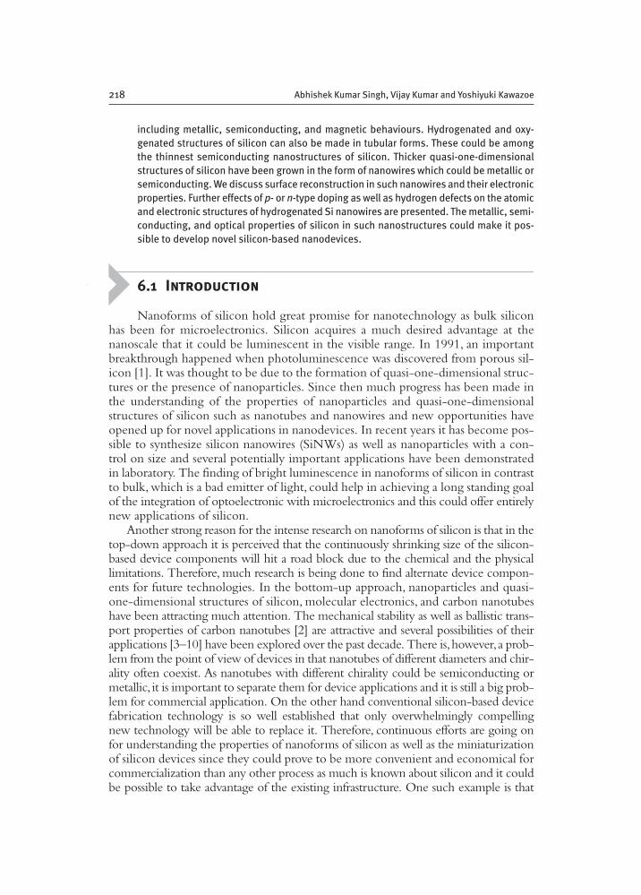
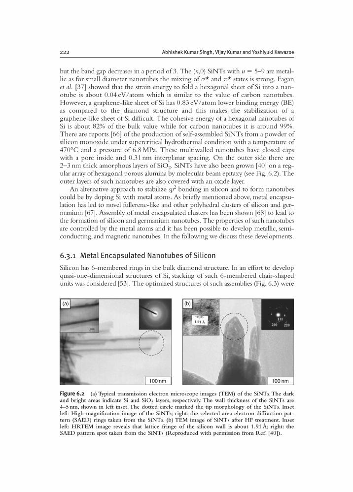
Figure 6.3 (a), (b), and (c) show optimized structures of SiNTs Si24, Si36, and Si48, respectively,formed by stacking of hexagonal units.The structures show preference for transformation fromquasi-one-dimensional to three-dimensional structures in the case of pure silicon. (d) Shows thestructural transformation that occurs from the chaired structure of Si12Be cluster to a hexagonalshape when two units of Si12Be are brought together to form nanotube. (e), (f ), and (g) show thefinite-doped Si24Bex (x � 2 and 3), Si36Bex (x � 3 and 5), and Si48Bex (x � 4 and 7) nanotubes,respectively. Groups I and II represent structures with the same number of Si and Be atoms buthaving different distributions of Be atoms, while the structures in Group III have higher concen-trations of Be atoms. It can be clearly seen that undoped part of nanotubes are distorted showingthe importance of Be atom doping. Group III shows an overdoping case which results in slightdistortion in the nanotube (adopted from Ref. [53]).

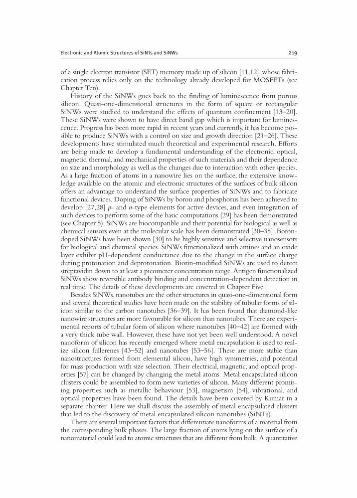
found to show a tendency for agglomeration to three-dimensional structures. Severalatoms tend to have tetrahedral coordination. This study showed the likelihood oflong symmetric thin tubular forms of elemental Si to be doubtful. It has been alsoshown by Grossman et al. [69] that the elongated structures with the number ofhexagonal units in the range of 10–29 can be stabilized by capping the ends with Siatoms. The stability could be further improved by replacing the capping element byB,Be, and N atoms. Also, similar to the case of hydrogen capped empty cage fullerenestructures of silicon [70], simulations on growth dynamics of hydrogenated siliconnanostructures have shown that nanotubular hexagonal form of silicon [71] could bestabilized by H termination (see below) in a controlled way (Fig. 6.4).
Studies on reaction of silane gas with metal monomers and dimers showed aSi12W cluster with W atom at the centre of a hexagonal prism to be favoured withoutassociating any H atoms [47]. This result suggested special stability of this cluster.Indeed the BE of H atom on this cluster was found [70] to be low and not favourablefor dissociation of a hydrogen molecule. Assembly of such clusters were also con-sidered to form a nanowire. However, it led to a distorted structure [70]. Further stud-ies on encapsulation of a variety of metal atoms in Si cages showed a chair-shaped
224 Abhishek Kumar Singh, Vijay Kumar and Yoshiyuki Kawazoe
(d)
(a) (b) (c)
Figure 6.4 Typical structures of hydrogenated silicon nanoparticles created in a plasma reactor.(a) Typical example for an amorphous structure resulting from a growth mechanism in a puresilane plasma at room temperature; aggregation of those amorphous particles leads to the exper-imentally observed formation of dust particles; (b) typical example for a low atomic hydrogenflux giving rise to crystalline structures that are rich in hydrogen; (c) typical example for a highatomic hydrogen flux yielding crystalline structures relatively poor in hydrogen that are similar tothose predicted for pure silicon clusters; (d) side and top view of a typical tube-like structureobtained with an intermediate atomic hydrogen flux. Hydrogen atoms are shown in white whilethe silicon atom inside is shown in red.The remaining atoms are Si atoms.The different colors ofother atoms are to distinguish different hexagons (Reproduced with permission from Ref. [71]courtesy H.Vach).
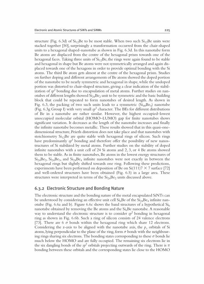
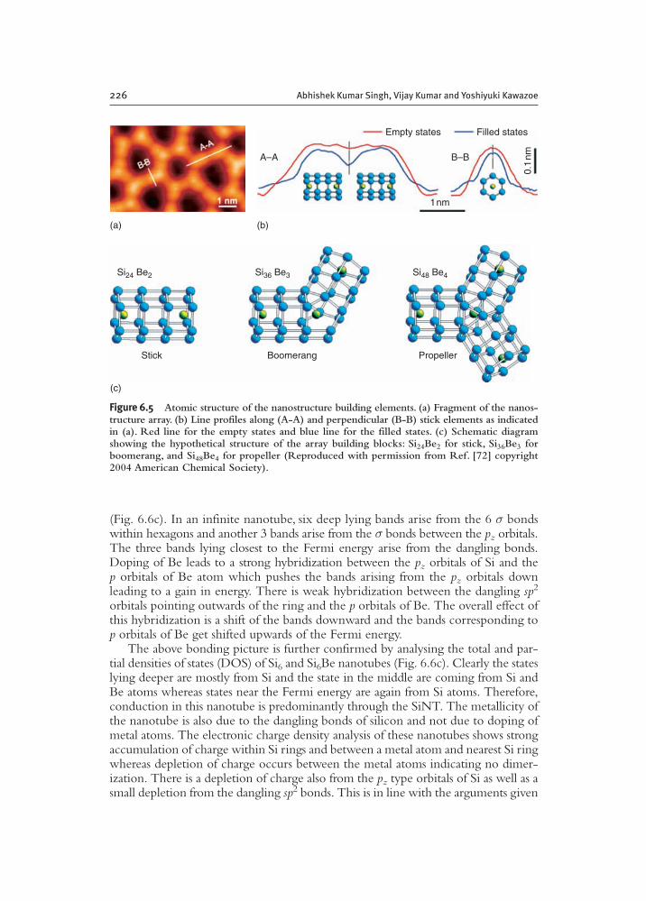
structure (Fig. 6.3d) of Si12Be to be most stable. When two such Si12Be units werestacked together [50], surprisingly a transformation occurred from the chair-shapedunits to a hexagonal shaped-nanotube as shown in Fig. 6.3d. In this nanotube formBe atoms are displaced from the centre of the hexagonal prism towards one of thehexagonal faces. Taking three units of Si12Be, the rings were again found to be stableand hexagonal in shape but Be atoms were not symmetrically arranged and again dis-placed towards one of the hexagons in order to provide optimal bonding with the Siatoms. The third Be atom gets almost at the centre of the hexagonal prism. Studieson further doping and different arrangements of Be atoms showed the doped portionof the nanotube to be nearly symmetric and hexagonal in shape,while the undopedportion was distorted to chair-shaped structure, giving a clear indication of the stabil-ization of sp2 bonding due to encapsulation of metal atoms. Further studies on nan-otubes of different lengths showed Si24Be2 unit to be symmetric and the basic buildingblock that could be repeated to form nanotubes of desired length. As shown in Fig. 6.3, the packing of two such units leads to a symmetric (Si48Be4) nanotube (Fig. 6.3g Group I) with very small sp3 character. The BEs for different distributionsof Be in a nanotube are rather similar. However, the highest occupied–lowestunoccupied molecular orbital (HOMO–LUMO) gap for finite nanotubes showssignificant variation. It decreases as the length of the nanotube increases and finallythe infinite nanotube becomes metallic. These results showed that in this quasi-one-dimensional structure, Peierls distortion does not take place and that nanotubes withstoichiometry Si12Be are quite stable with hexagonal rings of silicon. Such ringshave predominantly sp2 bonding and therefore offer the possibility of new nanos-tructures of Si stabilized by metal atoms. Further studies on the stability of dopedinfinite nanotubes with a unit cell of 24 Si atoms and 2, 3, or 4 Be atoms showedthem to be stable. As in finite nanotubes, Be atoms in the lowest energy structures ofSi24Be2, Si24Be3, and Si24Be4 infinite nanotubes were not exactly in between thehexagonal rings but slightly shifted towards one ring. Following these predictions,experiments have been performed on deposition of Be on Si(111)7 � 7 surface [72]and well-ordered structures have been obtained (Fig. 6.5) in a large area. Thesestructures were interpreted in terms of the Si24Be2 units discussed above.
6.3.2 Electronic Structure and Bonding Nature
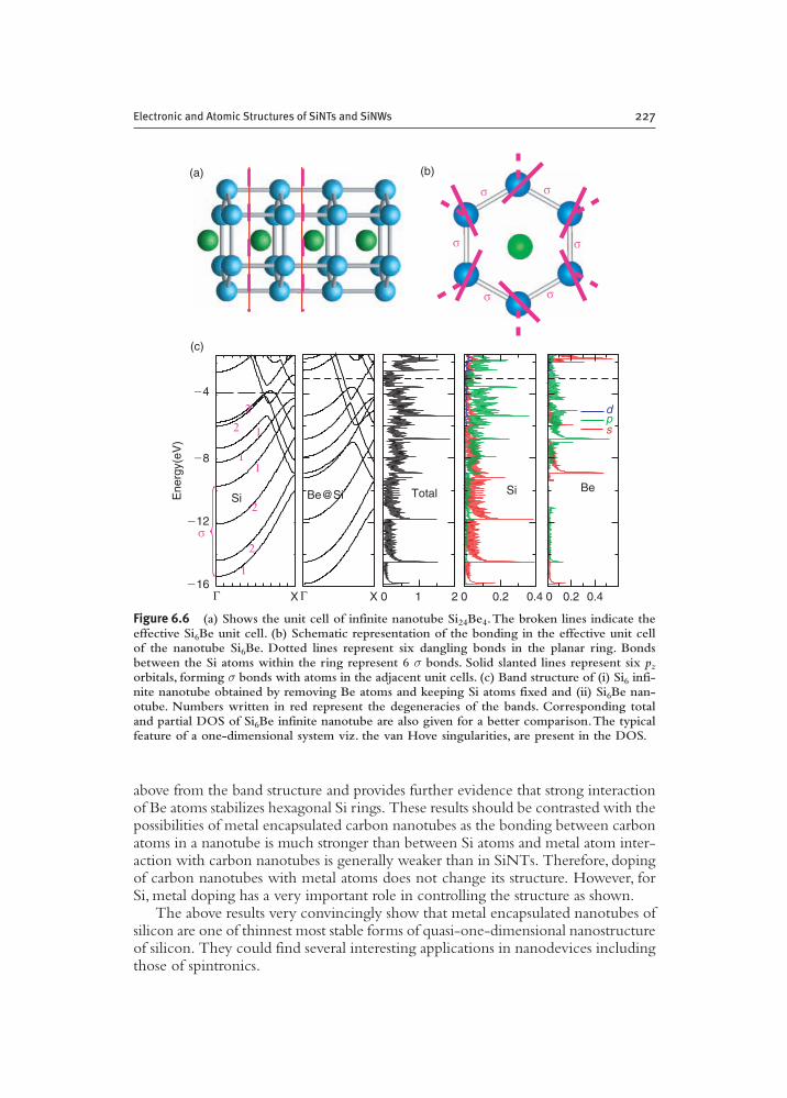
The electronic structure and the bonding nature of the metal encapsulated SiNTs canbe understood by considering an effective unit cell Si6Be of the Si24Be4 infinite nan-otube (Fig. 6.6a and b). Figure 6.6c shows the band structures of a hypothetical Si6nanotube obtained by removing the Be atoms and the Si6Be nanotube. A reasonableway to understand the electronic structure is to consider sp2 bonding in hexagonalring as shown in Fig. 6.6b. Such a ring of silicon consists of 24 valence electrons[73]. There are 6 σ bonds within the hexagonal ring which share 12 electrons.Considering the z-axis to be aligned with the nanotube axis, the pz orbitals of Siatoms, lying perpendicular to the plane of the ring, form σ bonds with the neighbour-ing rings sharing six electrons. The bonding states corresponding to these σ bonds liemuch below the HOMO and are fully occupied. The remaining six electrons lie inthe six dangling bonds of the sp2 orbitals projecting outwards of the ring. There is πbonding between these orbitals and the corresponding states lie close to the HOMO
Electronic and Atomic Structures of SiNTs and SiNWs 225
(Fig. 6.6c). In an infinite nanotube, six deep lying bands arise from the 6 σ bondswithin hexagons and another 3 bands arise from the σ bonds between the pz orbitals.The three bands lying closest to the Fermi energy arise from the dangling bonds.Doping of Be leads to a strong hybridization between the pz orbitals of Si and the p orbitals of Be atom which pushes the bands arising from the pz orbitals downleading to a gain in energy. There is weak hybridization between the dangling sp2
orbitals pointing outwards of the ring and the p orbitals of Be. The overall effect ofthis hybridization is a shift of the bands downward and the bands corresponding top orbitals of Be get shifted upwards of the Fermi energy.
The above bonding picture is further confirmed by analysing the total and par-tial densities of states (DOS) of Si6 and Si6Be nanotubes (Fig. 6.6c). Clearly the stateslying deeper are mostly from Si and the state in the middle are coming from Si andBe atoms whereas states near the Fermi energy are again from Si atoms. Therefore,conduction in this nanotube is predominantly through the SiNT. The metallicity ofthe nanotube is also due to the dangling bonds of silicon and not due to doping ofmetal atoms. The electronic charge density analysis of these nanotubes shows strongaccumulation of charge within Si rings and between a metal atom and nearest Si ringwhereas depletion of charge occurs between the metal atoms indicating no dimer-ization. There is a depletion of charge also from the pz type orbitals of Si as well as asmall depletion from the dangling sp2 bonds. This is in line with the arguments given
226 Abhishek Kumar Singh, Vijay Kumar and Yoshiyuki Kawazoe
A–A B–B
Empty states Filled states
0.1
nm
1nm
(a)
Si24 Be2
Stick Boomerang Propeller
Si36 Be3 Si48 Be4
(c)
(b)
Figure 6.5 Atomic structure of the nanostructure building elements. (a) Fragment of the nanos-tructure array. (b) Line profiles along (A-A) and perpendicular (B-B) stick elements as indicatedin (a). Red line for the empty states and blue line for the filled states. (c) Schematic diagramshowing the hypothetical structure of the array building blocks: Si24Be2 for stick, Si36Be3 forboomerang, and Si48Be4 for propeller (Reproduced with permission from Ref. [72] copyright2004 American Chemical Society).
above from the band structure and provides further evidence that strong interactionof Be atoms stabilizes hexagonal Si rings. These results should be contrasted with thepossibilities of metal encapsulated carbon nanotubes as the bonding between carbonatoms in a nanotube is much stronger than between Si atoms and metal atom inter-action with carbon nanotubes is generally weaker than in SiNTs. Therefore, dopingof carbon nanotubes with metal atoms does not change its structure. However, forSi, metal doping has a very important role in controlling the structure as shown.
The above results very convincingly show that metal encapsulated nanotubes ofsilicon are one of thinnest most stable forms of quasi-one-dimensional nanostructureof silicon. They could find several interesting applications in nanodevices includingthose of spintronics.
Electronic and Atomic Structures of SiNTs and SiNWs 227
σ
σ
σσ
σ
σ
(a) (b)
(c)
Si
σ
1
2
2
11
122
�16
�12
�8
�4
Ene
rgy(
eV)
0 0.2 0.4 0 0.2 0.4Γ X
Total Si BeBe@Si
dps
Γ X 20 1
Figure 6.6 (a) Shows the unit cell of infinite nanotube Si24Be4.The broken lines indicate theeffective Si6Be unit cell. (b) Schematic representation of the bonding in the effective unit cellof the nanotube Si6Be. Dotted lines represent six dangling bonds in the planar ring. Bondsbetween the Si atoms within the ring represent 6 σ bonds. Solid slanted lines represent six pzorbitals, forming σ bonds with atoms in the adjacent unit cells. (c) Band structure of (i) Si6 infi-nite nanotube obtained by removing Be atoms and keeping Si atoms fixed and (ii) Si6Be nan-otube. Numbers written in red represent the degeneracies of the bands. Corresponding totaland partial DOS of Si6Be infinite nanotube are also given for a better comparison.The typicalfeature of a one-dimensional system viz. the van Hove singularities, are present in the DOS.
6.3.3 Magnetism in Metal Encapsulated SiNTs
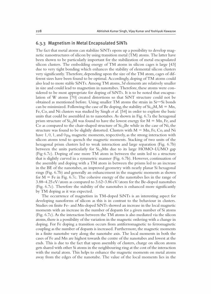
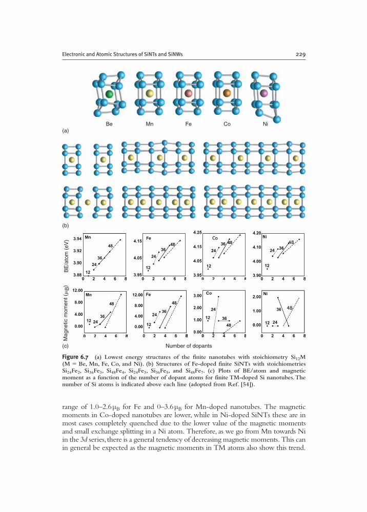
The fact that metal atoms can stabilize SiNTs opens up a possibility to develop mag-netic nanostructures of silicon by using transition metal (TM) atoms. The latter havebeen shown to be particularly important for the stabilization of metal encapsulatedsilicon clusters. The embedding energy of TM atoms in silicon cages is large [43]due to very tight bonding which enhances the stability of elemental silicon clustersvery significantly. Therefore, depending upon the size of the TM atom, cages of dif-ferent sizes have been found to be optimal. Accordingly, doping of TM atoms couldalso lead to more stable SiNTs. Among TM atoms, 3d elements are relatively smallerin size and could lead to magnetism in nanotubes. Therefore, these atoms were con-sidered to be most appropriate for doping of SiNTs. It is to be noted that encapsu-lation of W atoms [70] created distortions so that SiNT structure could not beobtained as mentioned before. Using smaller TM atoms the strain in Si!Si bondscan be minimized. Following the case of Be doping, the stability of Si12M,M � Mn,Fe, Co, and Ni clusters was studied by Singh et al. [54] in order to explore the basicunits that could be assembled in to nanotubes. As shown in Fig. 6.7a the hexagonalprism structure of Si12M was found to have the lowest energy for M � Mn, Fe, andCo as compared to the chair-shaped structure of Si12Be while in the case of Ni, thestructure was found to be slightly distorted. Clusters with M � Mn, Fe, Co, and Nihave 1, 0, 1, and 0 µB magnetic moments, respectively, as the strong interaction withsilicon atoms tend to quench the magnetic moments. Stacking of two units of thehexagonal prism clusters led to weak interaction and large separation (Fig. 6.7b)between the units particularly for Si12Mn due to its large HOMO–LUMO gap (Fig 6.7c). Doping of one more TM atom in between the units led to a structurethat is slightly curved in a symmetric manner (Fig. 6.7b). However, continuation ofthe assembly and doping with a TM atom in between the prisms led to an increasein the BE of the nanotubes, an improved geometry with nearly planar Si hexagonalrings (Fig. 6.7b) and generally an enhancement in the magnetic moments as shownfor M � Fe in Fig. 6.7c. The cohesive energy of the nanotubes lies in the range of3.88–4.25 eV/atom as compared to 3.62–3.86 eV/atom for the Be-doped nanotubes(Fig. 6.7c). Therefore the stability of the nanotubes is enhanced more significantlyby TM doping as it was expected.
The occurrence of magnetism in TM-doped SiNTs is an interesting aspect fordeveloping nanoforms of silicon as this is in contrast to the behaviour in clusters.Studies on finite Fe- and Mn-doped SiNTs showed an increase in the local magneticmoments with an increase in the number of dopants for a given number of Si atoms(Fig. 6.7c). As the interaction between the TM atoms is also mediated via the siliconatoms, there is a possibility of the variation in the magnetic ordering with a change indoping. For Fe doping a transition occurs from antiferromagnetic to ferromagneticcoupling as the number of dopants is increased. Furthermore, the magnetic momentsin a finite nanotube vary along the nanotube axis. The local moments in both thecases of Fe and Mn are highest towards the centre of the nanotubes and lowest at theends. This is due to the fact that upon assembly of clusters, charge on silicon atomsgets shared with other Si atoms in the neighbouring ring at the cost of the interactionwith the metal atom. This helps to enhance the magnetic moments on metal atomsaway from the edges of the nanotube. The value of the local moments lies in the
228 Abhishek Kumar Singh, Vijay Kumar and Yoshiyuki Kawazoe
Electronic and Atomic Structures of SiNTs and SiNWs 229
(a)Be Mn Fe Co Ni
(b)
(c)
BE
/ato
m (
eV)
Number of dopants
Mag
netic
mom
ent (
�B
)
Figure 6.7 (a) Lowest energy structures of the finite nanotubes with stoichiometry Si12M(M � Be, Mn, Fe, Co, and Ni). (b) Structures of Fe-doped finite SiNTs with stoichiometriesSi24Fe2, Si36Fe3, Si48Fe4, Si24Fe3, Si36Fe5, and Si48Fe7. (c) Plots of BE/atom and magneticmoment as a function of the number of dopant atoms for finite TM-doped Si nanotubes.Thenumber of Si atoms is indicated above each line (adopted from Ref. [54]).
range of 1.0–2.6 µB for Fe and 0–3.6 µB for Mn-doped nanotubes. The magneticmoments in Co-doped nanotubes are lower, while in Ni-doped SiNTs these are inmost cases completely quenched due to the lower value of the magnetic momentsand small exchange splitting in a Ni atom. Therefore, as we go from Mn towards Niin the 3d series, there is a general tendency of decreasing magnetic moments. This canin general be expected as the magnetic moments in TM atoms also show this trend.
When Si12M cluster units interact to form a nanotube, there is an increase in theSi!Si and TM!Si bond lengths. A similar increase in the cage size was obtained[70] due to the capping of H atoms on metal encapsulated clusters of silicon such asSi12Cr. It led to the development of magnetic moments in this cluster due to theweakening of the interaction between the cage and the metal atom. H termination ofthese clusters has a similar effect as the linking between the clusters in nanotubes. Thisis further supported from the fact that a small or zero local magnetic moment is foundon metal atoms that lie towards the edges of the finite nanotubes while large momentsoccur on atoms that are away from the edges of the nanotubes. The high magneticmoments of Si48Fe7 (1.7 µB per Fe atom) and Si48Mn7 (1.6 µB per Mn atom) suggestthat such nanotubes could be useful for magnetic device applications.
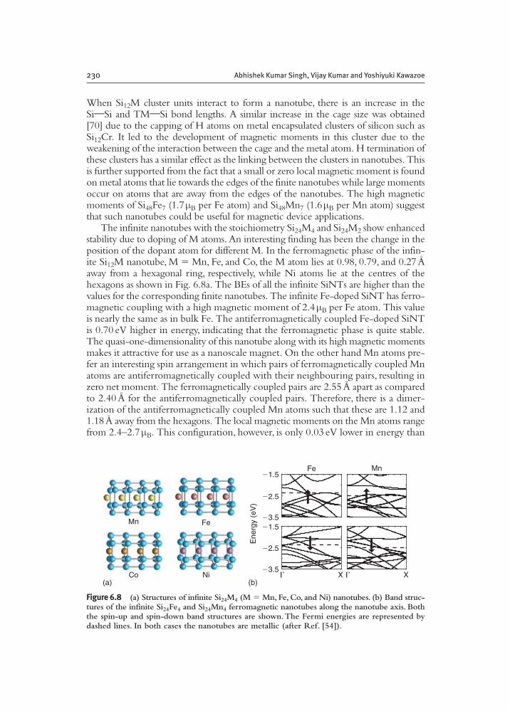
The infinite nanotubes with the stoichiometry Si24M4 and Si24M2 show enhancedstability due to doping of M atoms. An interesting finding has been the change in theposition of the dopant atom for different M. In the ferromagnetic phase of the infin-ite Si12M nanotube, M � Mn, Fe, and Co, the M atom lies at 0.98, 0.79, and 0.27Åaway from a hexagonal ring, respectively, while Ni atoms lie at the centres of thehexagons as shown in Fig. 6.8a. The BEs of all the infinite SiNTs are higher than thevalues for the corresponding finite nanotubes. The infinite Fe-doped SiNT has ferro-magnetic coupling with a high magnetic moment of 2.4 µB per Fe atom. This valueis nearly the same as in bulk Fe. The antiferromagnetically coupled Fe-doped SiNTis 0.70 eV higher in energy, indicating that the ferromagnetic phase is quite stable.The quasi-one-dimensionality of this nanotube along with its high magnetic momentsmakes it attractive for use as a nanoscale magnet. On the other hand Mn atoms pre-fer an interesting spin arrangement in which pairs of ferromagnetically coupled Mnatoms are antiferromagnetically coupled with their neighbouring pairs, resulting inzero net moment. The ferromagnetically coupled pairs are 2.55 Å apart as comparedto 2.40 Å for the antiferromagnetically coupled pairs. Therefore, there is a dimer-ization of the antiferromagnetically coupled Mn atoms such that these are 1.12 and1.18Å away from the hexagons. The local magnetic moments on the Mn atoms rangefrom 2.4–2.7 µB. This configuration, however, is only 0.03 eV lower in energy than
230 Abhishek Kumar Singh, Vijay Kumar and Yoshiyuki Kawazoe
Mn Fe
Co Ni(a) (b)
Fe Mn
Ene
rgy
(eV
)
�3.5
�2.5
�1.5
�3.5
�2.5
�1.5
� X � X
Figure 6.8 (a) Structures of infinite Si24M4 (M � Mn, Fe,Co, and Ni) nanotubes. (b) Band struc-tures of the infinite Si24Fe4 and Si24Mn4 ferromagnetic nanotubes along the nanotube axis. Boththe spin-up and spin-down band structures are shown.The Fermi energies are represented bydashed lines. In both cases the nanotubes are metallic (after Ref. [54]).
the corresponding ferromagnetically coupled SiNT. This result shows that a trans-formation from antiferromagnetic to ferromagnetic coupling in the Mn-doped nan-otubes may be achieved by application of a weak magnetic field and suggests thatspin-polarized current flow could be controlled by applying a magnetic field. TheBE for the Mn-doped nanotube is almost 90% of the bulk cohesive energy of Siwithin GGA. For the Co- and Ni-doped infinite SiNTs, ferromagnetic and antifer-romagnetic starting configurations converge to non-magnetic solutions and there-fore in these cases the SiNTs are non-magnetic.
Figure 6.8b shows the band structures of Fe- and Mn-doped SiNTs. In all casesthere is band crossing at the Fermi level for both the spin-up and spin-down compon-ents, indicating metallic behaviour. The band structure of the Mn-doped ferromag-netic nanotube shows a gap just above the Fermi energy for the spin-up componentand therefore there could be interesting possibilities of making half-metallic nanotubesby inducing a small shift in the Fermi energy such as by doping. The antiferromag-netic Mn-doped nanotube shows a quite different band structure, as the periodicitiesin the two cases are different. Thus, doping of TM atoms leads to enhanced stabilityof SiNTs and new possibilities of magnetic nanostructures of silicon.
It is interesting to mention here that the hexagonal SiNTs have similarity with therare earth-doped SiNWs grown on a Si substrate [74–77]. In this case the hexagonaltubes are linked and form a strip. Andriotis et al. [56] have shown that V doping couldalso lead to the formation of SiNTs with similar structure. The nanotubes obtainedby Andriotis et al. were also metallic and have slight magnetic moment. Furthermore,Dumitric et al. [78] have studied the stability of metal encapsulated SiNTs with sev-eral TM atoms as well as various other structural variations (see also Chapter Eight).They also concluded hexagonal ring-based SiNTs to be the most stable among vari-ous phases. Similar to the results of the previous studies [53,54], they also found thesenanotubes to be metallic. Further studies on the mechanical properties of the SiNTsshowed high mechanical stability.
6.4 Germanium nanotubes
Similar to SiNTs, metal encapsulated clusters of Ge can be used as buildingblocks for novel nanoforms of Ge. An important aspect here is that Ge atom is about4% bigger in size as compared to Si. This could lead to the possibility of doping withslightly bigger atoms as well as making different structures of Ge nanotubes (GeNTs)while the more extended nature of Ge valence orbitals may give rise to different prop-erties. In order to find suitable building blocks of GeNTs, Singh et al. [68,79] per-formed a search for the most favourable structure of Ge12Mn cluster by optimizingicosahedral, decahedral, hexagonal prism, and hexagonal antiprism structures. UnlikeSi12Mn cluster that has the hexagonal prism structure [80], Ge12Mn favours a perfecticosahedral structure, which has high coordination and high magnetic moment of5 �B. However, another nearly degenerate isomer with hexagonal antiprism structurehas a small magnetic moment of 1 �B. Both the icosahedral and hexagonal isomerswere found to possess large HOMO–LUMO gaps of 1.11 and 1.13eV, respectivelyand therefore are very stable, suggesting the possibility of their assemblies into nan-otubes and other forms.
Electronic and Atomic Structures of SiNTs and SiNWs 231
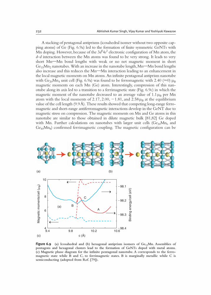
A stacking of pentagonal antiprisms (icosahedral isomer without two opposite cap-ping atoms) of Ge (Fig. 6.9a) led to the formation of finite symmetric GeNTs withMn doping. However, because of the 3d54s2 electronic configuration of Mn atom, thed–d interaction between the Mn atoms was found to be very strong. It leads to veryshort Mn!Mn bond lengths with weak or no net magnetic moment in shortGe15Mn2 nanotubes. With an increase in the nanotube length,Mn!Mn bond lengthsalso increase and this reduces the Mn!Mn interaction leading to an enhancement inthe local magnetic moments on Mn atoms. An infinite pentagonal antiprism nanotubewith Ge20Mn4 unit cell (Fig. 6.9a) was found to be ferromagnetic with 2.40 (�0) µBmagnetic moments on each Mn (Ge) atom. Interestingly, compression of this nan-otube along its axis led to a transition to a ferrimagnetic state (Fig. 6.9c) in which themagnetic moment of the nanotube decreased to an average value of 1.1 µB per Mnatom with the local moments of 2.17, 2.00, �1.81, and 2.58 µB at the equilibriumvalue of the cell length (9.9Å). These results showed that competing long-range ferro-magnetic and short-range antiferromagnetic interactions develop in the GeNT due tomagnetic stress on compression. The magnetic moments on Mn and Ge atoms in thisnanotube are similar to those obtained in dilute magnetic bulk [81,82] Ge doped with Mn. Further calculations on nanotubes with larger unit cells (Ge30Mn6 andGe40Mn8) confirmed ferrimagnetic coupling. The magnetic configuration can be
232 Abhishek Kumar Singh, Vijay Kumar and Yoshiyuki Kawazoe
(c) c (Å)
Mag
netic
mom
ents
/cel
l (�
B)
Bin
ding
ene
rgy/
cell
(eV
)
10
8
6
49.4 9.8 10.2 10.6
�98.1
�98.2
�98.3
�98.4
(a) B
C
A
(a) (b)
Figure 6.9 (a) Icosahedral and (b) hexagonal antiprism isomers of Ge12Mn. Assemblies ofpentagons and hexagonal clusters lead to the formation of GeNTs doped with metal atoms.(c) Magnetic phase diagram for the infinite pentagonal nanotube. A corresponds to the ferro-magnetic state while B and C, to ferrimagnetic states. B is marginally metallic while C is semiconducting (adopted from Ref. [79]).
described in terms of ferromagnetically coupled nano-domains and patches of anti-ferromagnetically coupled spins. The antiferromagnetically coupled Mn atoms haveshorter Mn!Mn bond lengths compared with ferromagnetically coupled Mn atomsleading to a reduction in the magnetic stress of the nanotubes on compression.
The band structures of GeNT in different phases with a Ge20Mn4 unit cell showthat the ferromagnetic phase (A in Fig. 6.9c) is metallic, but the ferrimagnetic phaseat the equilibrium cell length of 9.9 Å is only marginally metallic with few holes inthe valence band and a few electrons in the conduction band for spin-up and spin-down states, respectively. Further calculations with an expanded lattice constant inthe ferrimagnetic phase showed a shallow minimum (C) in which the nanotube issemiconducting with a small band gap and 1 µB magnetic moment per Mn atom.As the GGA underestimates the band gap, it was suggested that the true groundstate of the ferrimagnetic phase (B) could also be semiconducting. Compression ofthe nanotube beyond the cell length 9.9 Å leads to more metallic behaviour of theferrimagnetic GeNT in which the local magnetic moments change, though the netmagnetic moment per cell remains nearly the same leading to a relatively shallowregion in the phase diagram.
A stacking of hexagonal rings in an antiprism structure also leads to highly sym-metric GeNT (Fig. 6.9b) with significantly higher magnetic moments on Mn atomsthan in the case of the pentagonal nanotubes. The behaviour of these hexagonalGeNTs is very similar to SiNTs as there is a weak interaction between the clustersdue to the magic nature of Ge12Mn and its large HOMO–LUMO gap. This alsoleads to large intercluster separation for the dimer and makes ferromagnetic (2 µB) aswell as antiferromagnetic (0 µB) spin isomers nearly degenerate. Doping of an Mnatom in between two hexagonal Ge12Mn clusters leads to antiferromagnetic couplingbetween the Mn atoms and a reduction in the Ge!Ge intercluster separation.Similar to the case of the SiNTs, the enhanced interaction between the clusters dueto the reduction in the intercluster Ge!Ge bond lengths leads to an increase in thelocal magnetic moments on Mn atoms. As the length of the nanotube increases, thereis further shortening of the intercluster Ge!Ge bond lengths and delocalization ofelectrons in the nanotubes. The ferromagnetic and antiferromagnetic spin-isomersgenerally lie close in energy for the finite nanotubes but the infinite GeNT favoursferromagnetic ordering. An infinite nanotube with a unit cell of Ge24Mn4 is verysymmetric and the local magnetic moments are the highest among the M-dopednanotubes with the value of 3.41 µB on each Mn atom. There is a small-inducedpolarization of opposite spin (0.05 µB) on each Ge atom leading to 3.06 µB averagemagnetic moment per Mn atom. This behaviour remains even when the nanotube iscompressed suggesting that it is a good nanomagnet. The band structure of the infi-nite hexagonal antiprism nanotube shows band crossing at the Fermi level for thespin-up as well as spin-down components, indicating metallic behaviour.
6.4.1 Metallic and Semiconducting Nanotubes of Ge
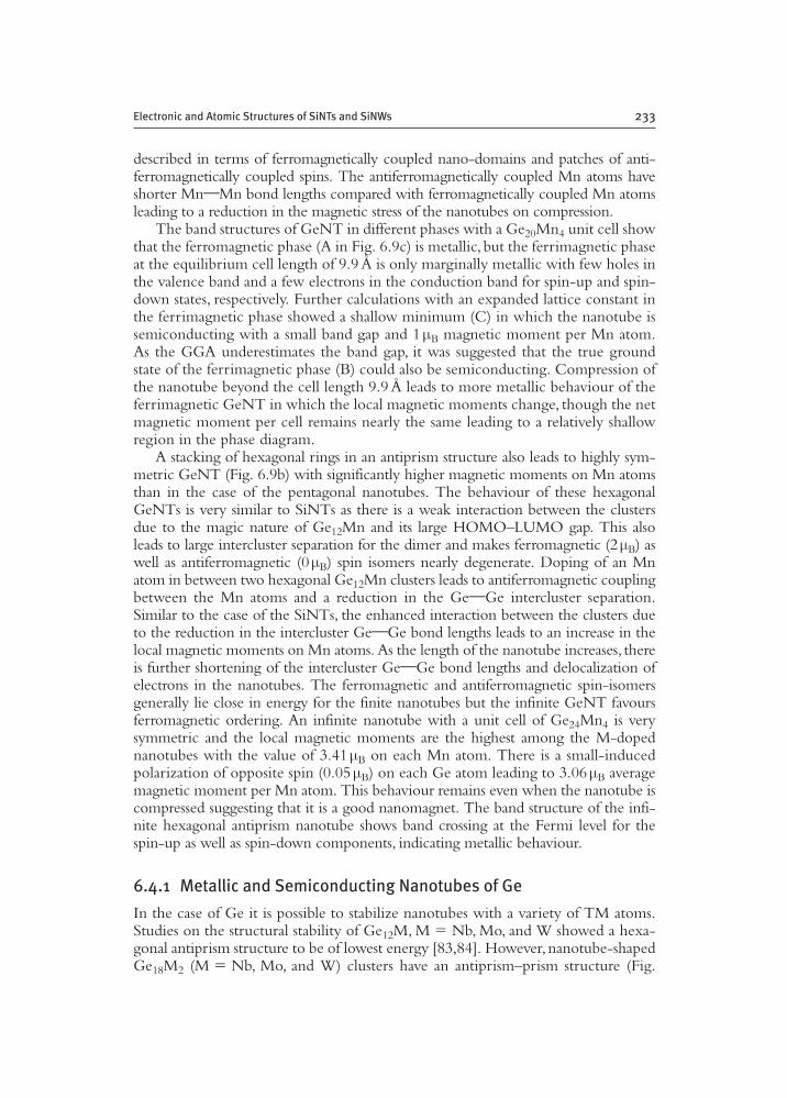
In the case of Ge it is possible to stabilize nanotubes with a variety of TM atoms.Studies on the structural stability of Ge12M, M � Nb, Mo, and W showed a hexa-gonal antiprism structure to be of lowest energy [83,84]. However,nanotube-shapedGe18M2 (M � Nb, Mo, and W) clusters have an antiprism–prism structure (Fig.
Electronic and Atomic Structures of SiNTs and SiNWs 233
6.10a) which is 0.44, 0.55, and 0.59 eV lower in energy for M � Nb, Mo, and W,respectively compared to a biprism structure which was found to be lowest inenergy for Si18W2. A prism–prism structure of GeNT lies second in energy with alonger M!M bond while an antiprism–antiprism structure lies highest in energywith shorter M!M bond. The prism–antiprism structure optimizes M!M as wellas Ge!Ge and Ge!M interactions. The HOMO–LUMO gap for this finite nan-otube with M � Nb and W is 0.33 and 1.03 eV, respectively. Infinite GeNTs wereobtained by assembling Ge18M2 clusters. When two clusters of Ge18Nb2 are assem-bled together with a Nb atom in between (Ge36Nb5), then the antiprism–prismstructure remains stable as shown in Fig. 6.10b. This structural growth also got sup-port from a calculation in which an antiprism–antiprism stacking of hexagonstransformed to the antiprism–prism structure. Therefore, the preference forprism–antiprism structure did not change with an increase in the length of the nan-otube. Further addition of a Ge12Nb cluster keeps this structure very symmetric(Fig. 6.10d) but with increasing length, a slightly different stacking in which thecentral four hexagons are in the antiprism structure, lies only 0.05 eV higher inenergy. These results showed that the rotation of a hexagon costs little energy as thelength of the nanotube increases, though for an infinite nanotube theantiprism–prism staking remains lowest in energy (Fig. 6.10d). The BE of the nan-otube was found to increase with an increase in the number of clusters and thereforenanotubes can be formed with a large aspect ratio. The HOMO–LUMO gap in finite
234 Abhishek Kumar Singh, Vijay Kumar and Yoshiyuki Kawazoe
(a) (b) (c)
(e)
(d)
k
−6
−5
−4
−3
−2
0.0 0.1 0.2 0.3 0.4 0.5
Ene
rgy
(eV
)
NbEg
0.0 0.1 0.2 0.3 0.4 0.5
W
Figure 6.10 (a), (b), and (c) show optimized structures of finite nanotubes Ge18M2, Ge36M5,and Ge48M7, respectively. These structures are similar for M � Nb, Mo, and W though Nb-doped nanotubes are slightly distorted while Mo- and W-doped nanotubes are very sym-metric. (d) shows the optimized unit cell of infinite nanotube Ge24M4 with Ge12M clustersstacked in prism and antiprism structures. (e) Band structures of Nb- and W-doped infinitenanotubes. Dashed line shows the Fermi energy. Eg is the band gap for the W-doped semicon-ducting nanotube (adopted from Ref. [83]).
nanotubes is small and the infinite GeNT becomes metallic with a unit cell ofGe24Nb4.
The band structure of an infinite Ge24Nb4 nanotube shows (Fig. 6.10e) a gap justabove the Fermi level indicating the possibility of the formation of a semiconductingnanotube by the filling of these states. Indeed when all Nb atoms were replaced withMo, the extra electron filled the empty states near the Fermi level and the nanotubebecame 6-fold symmetric and semiconducting with a band gap of 0.38eV (Fig. 6.10e).Similar results were also obtained for W-doped GeNT. Therefore, unlike SiNT,doping of Mo or W in GeNT led to the formation of a semiconducting nanotubewith a direct band gap. The band gap is higher for W doping with the GGA value of0.5 eV. The Ge18Mo2 and Ge36Mo5 finite nanotubes were also found to have smallerHOMO–LUMO gaps of 0.96 and 0.75 eV as compared to 1.03 and 1.01 eV, respect-ively for W doping. The true values of the band gap in the infinite nanotubes isexpected to be around 1 eV which is comparable to the value for bulk silicon.Therefore,W-doped GeNT could open up new possibilities for device developmentat the smallest scale. The BE for the W-doped infinite nanotube is 4.04 eV/atom ascompared to 3.81 eV/atom for Mo doping. Therefore, W doping is better fromenergetic point of view as well.
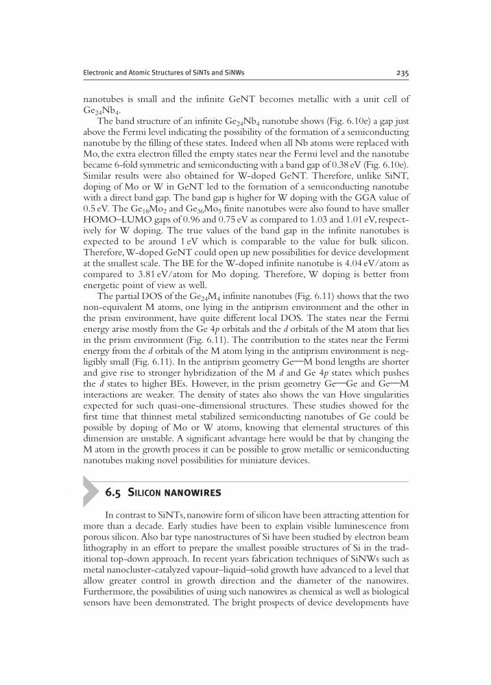
The partial DOS of the Ge24M4 infinite nanotubes (Fig. 6.11) shows that the twonon-equivalent M atoms, one lying in the antiprism environment and the other inthe prism environment, have quite different local DOS. The states near the Fermienergy arise mostly from the Ge 4p orbitals and the d orbitals of the M atom that liesin the prism environment (Fig. 6.11). The contribution to the states near the Fermienergy from the d orbitals of the M atom lying in the antiprism environment is neg-ligibly small (Fig. 6.11). In the antiprism geometry Ge!M bond lengths are shorterand give rise to stronger hybridization of the M d and Ge 4p states which pushesthe d states to higher BEs. However, in the prism geometry Ge!Ge and Ge!Minteractions are weaker. The density of states also shows the van Hove singularitiesexpected for such quasi-one-dimensional structures. These studies showed for thefirst time that thinnest metal stabilized semiconducting nanotubes of Ge could bepossible by doping of Mo or W atoms, knowing that elemental structures of thisdimension are unstable. A significant advantage here would be that by changing theM atom in the growth process it can be possible to grow metallic or semiconductingnanotubes making novel possibilities for miniature devices.
6.5 SILICON nanowires
In contrast to SiNTs,nanowire form of silicon have been attracting attention formore than a decade. Early studies have been to explain visible luminescence fromporous silicon. Also bar type nanostructures of Si have been studied by electron beamlithography in an effort to prepare the smallest possible structures of Si in the trad-itional top-down approach. In recent years fabrication techniques of SiNWs such asmetal nanocluster-catalyzed vapour–liquid–solid growth have advanced to a level thatallow greater control in growth direction and the diameter of the nanowires.Furthermore, the possibilities of using such nanowires as chemical as well as biologicalsensors have been demonstrated. The bright prospects of device developments have
Electronic and Atomic Structures of SiNTs and SiNWs 235
led to the fabrication of SiNWs in many laboratories and in recent years their appli-cations have also been explored extensively. More details about the experimentaldevelopments can be found in Chapter Five as well as by Durrani and Ahmad(Chapter Ten) who also discuss SiNW-based SET. In the subsequent sections wepresent a review of theoretical studies on the atomic and electronic structures of thesesystems and show how first principles studies can help to the development of this classof materials.
236 Abhishek Kumar Singh, Vijay Kumar and Yoshiyuki Kawazoe
0
1
2
3
0
2
4
6
8
−4 −3−5 −2
0.0
0.4
0.8
1.2
−5 −4 −3 −2
0
2
4
6
8
EF
Nb
Metallic Semiconducting
Eg
DO
S/a
tom
Energy(eV)
W
Figure 6.11 Total and partial DOS for Nb- and W-doped infinite GeNTs. (a) Total DOS,(b) partial DOS of Ge, (c) partial DOS for Nb atom in the antiprism environment, and (d) partialDOS for the Nb atom in the prism environment of Ge. Red, green, and blue lines representcontributions from s, p, and d orbitals, respectively. Dashed line shows the Fermi energy (EF),while for the W-doped semiconducting nanotube the band gap is indicated by an arrow(adopted from Ref. [83]).
Theoretical studies on SiNWs can be classified into two categories: (1) Novelstructures formed from assembly of clusters and (2) nanowires having bulk silicon-like structure. In the latter case the properties could depend sensitively on the morph-ology and the direction of the axis along which the cut is made. In experimentssurfaces of SiNWs of category (2) are generally passivated with hydrogen or oxy-gen and the atomic structure is mostly crystalline at least inside the nanowires whilesome changes may take place on the surface depending upon the morphology andthe growth conditions used. On the other hand properties of pristine SiNWs coulddepend strongly on surface reconstructions. In this section we focus on (1) non-crystalline pristine SiNWs that are based on assembly of novel clusters of Si, (2) crys-talline pristine SiNWs,and (3) hydrogenated SiNWs. Finally we discuss some studieson Si/Ge core-shell nanowires as well as nanowire superlattices.
6.5.1 Non-Crystalline Pristine SiNWs
Similar to metal encapsulated Si/GeNTs where metal encapsulated clusters areassembled to form tubuler structures, nanowire structures of pristine silicon couldbe produced by assembly of stable elemental Si clusters and they could offer a newform of silicon with novel properties. A few possibilities of such assemblies havebeen explored. Experimentally at least 100 nm long SiNWs of 3–7 nm diameterhave been prepared by depositing silicon vapour onto highly oriented pyrolyticgraphite [85]. These nanowires were assembled parallel in bundles and their atomicstructure was modelled in terms of aggregation of small Si clusters whose size ismuch smaller than the diameter of the nanowires. From total energy calculationson a few selected cluster assembled SiNWs, it was shown that the atomic structurebased on an assembly of fullerene-shaped Si24 clusters was lowest in energy. Thesestructures are inherently metastable as pure Sin clusters with n � 20 prefer elong-ated or three-dimensional structures [86,87] rather than empty cage fullerenes. Thestabilization of SiNW with Si24 fullerene cages could be similar to the stabilizationof fullerene cages of silicon with H termination. For pure silicon clusters, a transitionto nearly spherical three-dimensional compact structures at n � 27 is related to theonset of the formation of structures [87,88] that are composed of fullerene-like cageswith a small number of silicon atoms inside. These results also give a clear indicationof the difficulty in forming very thin nanowires or nanotubes of silicon which requireconditions that allow only one-dimensional growth such as in vapour–liquid–solidgrowth using metal clusters as seeds.
Theoretical studies have been done on a few assemblies of clusters. Thin SiNWswith length up to 26 Å formed [89] from an assembly of Si9 tricapped trigonal prism(TTP) units and uncapped trigonal prisms as the building blocks were shown to bestable using full-potential linear muffin-tin orbital calculations. The HOMO–LUMOgap of these finite nanowires approaches zero value with increasing length. Menonand Richter [90] have studied quasi-one-dimensional structures of Si using a gen-eralized tight binding molecular dynamics method and shown that SiNW structurescould be stable if the core atoms are 4-fold coordinated and are surrounded by 3-foldcoordinated surface atoms. The latter are arranged in such a way so as to form one ofthe most stable reconstructions known on bulk silicon surfaces such as the buckleddimer formation on Si(100) surface or the (7 � 7) reconstruction on Si(111) surface.
Electronic and Atomic Structures of SiNTs and SiNWs 237
Because of the presence of dangling bonds, surface of such a nanowire was suggestedto be reactive. The building blocks of these SiNWs are multiply connected clusterswith a small hollow region in the middle. The electronic structure of such as infinitenanowires showed them to be semiconducting with a slightly smaller band gap com-pared with bulk Si.
6.5.2 Crystalline Pristine SiNWs
Studies on crystalline pristine SiNWs have been done by considering a cut from bulksilicon such as a square-shaped [001] oriented SiNW. The fraction of atoms lying onthe surface of such a thin nanowire is quite large and the properties of such nanowirescould be affected significantly by changes on the surface such as by reconstructionand adsorption. This is also a reason for the molecular level sensitivity of the SiNWsin contrast to bulk whose properties are affected little by the presence of surface.Similar to the reconstructions on bulk Si surfaces, reconstruction could be expectedon pristine SiNW surface. However, such studies are only few and the physics andchemistry of SiNW surfaces are yet to be fully developed. There are several naturalquestions that need to be addressed. Among these, the effects of large surface to bulkratio on the structural, electrical,mechanical, vibrational, and doping behaviour of thenanowires are very prominent. As compared to bulk surfaces, nanowires have facetsthat have infinite extent only in one of the lateral directions and finite in the other.The edges, i.e. the intersection of two facets could have significant effect on surfacereconstruction of a nanowire and the morphology. Such effects become more import-ant as the diameter of nanowire decreases because surface states may be responsible forconductance in such SiNWs and it may itself be larger than expected from dopedSiNWs. Therefore, pristine SiNWs may not need doping for conduction. In generalappropriate doping ways may be needed to tailor the electrical properties of SiNWsand control statistical fluctuations in doping concentration as well as distribution fromone wire to another. Answering these questions by experiments alone could be diffi-cult and ab initio studies could prove to be an important tool in this regard.
A comprehensive study to identify the importance of edges and their effects onthe properties of SiNWs was carried out by Ismail-Beigi and Arias [91] on SiNWsoriented along the [001] axis. A nanowire with octagonal cross-section was con-structed using Wulff construction by removing corner atoms from an initially square-shaped nanowire. At the edges of such a nanowire {110} facets meet {100} facets. Allatoms on the surface of this nanowire are 2-fold coordinated without atomic relax-ation. Studies on bulk Si (001) surface have shown 2 � 1 (or p(2 � 2)) andc(2 � 2) reconstructions to be competitive, though p(2 � 2) reconstruction has thelowest energy [92]. When the structure of SiNW was relaxed, two competing low-energy reconstructions on the {100} surface of SiNWs were found: (1) that best sat-isfies the system in terms of the total number of bonds with optimal bonding alongthe edges and (2) that best satisfies the system in terms of the lowest energy config-uration of the surfaces. For a given size of the nanowires, a balance has to be madebetween the two and therefore the reconstructions are size dependent. They found aunique surface atom with which each edge atom may bind to become 3-fold coord-inated, but it affects reconstruction on {100} facets which favour c(2 � 2) typereconstruction. Therefore an edge-driven transition from p(2 � 2) reconstruction on
238 Abhishek Kumar Singh, Vijay Kumar and Yoshiyuki Kawazoe
large diameter nanowires (similar to the one favoured on bulk (001) surface) to thec(2 � 2) reconstruction occurred as the cross-section of the nanowire was decreasedbelow the value of around 3.0 � 3.0nm. The c(2 � 2) reconstruction maximizes thenumber of bonds in the system and it overcomes the cost in changing the natural ten-dency of the surfaces. In SiNWs with the p(2 � 2) surface reconstruction there is adoubling of the periodicity along the nanowire axis and half the atoms on edges are2-fold coordinated. Because of bonding restrictions into the interior of the structure,the dimer rows in alternate faces have patterns of 2 � 1 reconstruction as shown inFig. 6.12. The reconstruction was shown to have an effect on the electronic structureas the surface states could depend on the type of reconstruction, but little change inthe elastic properties of the nanowires.
The effects of edges on the atomic structure of SiNWs have also been consideredby Zhao and Yakobson [93] who studied SiNWs with large diameters using a tightbinding molecular dynamics method. Nanowires with pentagonal cross-section({100} facets) and hexagonal cross-section (four {111} and two {100} facets) wereconsidered. The ground state of the nanowires with diameters (d) �6nm was foundto be polycrystalline with 5-fold rotational symmetry. Also a nanowire made of Si20fullerenes was found to have lowest energy in this family of structures.
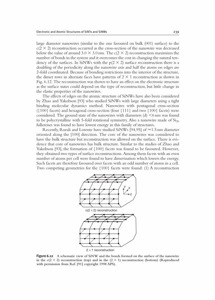
Recently, Rurali and Lorente have studied SiNWs [94,95] of �1.5 nm diameteroriented along the [100] direction. The core of the nanowires was considered tohave the bulk structure but reconstruction was allowed on the surface. There is evi-dence that core of nanowires has bulk structure. Similar to the studies of Zhao andYakobson [93], the formation of {100} facets was found to be favoured. However,they obtained two types of surface reconstructions. Among them facets with an evennumber of atoms per cell were found to have dimerization which lowers the energy.Such facets are therefore favoured over facets with an odd number of atoms in a cell.Two competing geometries for the {100} facets were found: (1) A reconstruction
Electronic and Atomic Structures of SiNTs and SiNWs 239
c(2 × 2) reconstruction
2 × 1 reconstruction
y x
z
Figure 6.12 A schematic view of SiNW and the bonds formed on the surface of the nanowirein the c(2 � 2) reconstruction (top) and in the (2 � 1) reconstruction (bottom) (Reproducedwith permission from Ref. [91] copyright 1998 APS).
(see Fig. 6.13a) with the same periodicity as the cell along the unreconstructed wire,has a trough in the middle of the facet and it turns out to be the most stable and (2) a reconstruction (see Fig. 6.13b) with twice the periodicity of (1) which is only3 meV/atom higher indicating that both reconstructions are likely to coexist. Thetrough in reconstruction (1) is determined by the buckled dimer sequence whichpresents a double chain of low atoms (labeled with a circle in Fig. 6.13). This isobserved in only one of the two sides in reconstruction (2) while on the other side,one out of every two dimers is flipped. Interestingly, no direct correspondence wasfound with infinite surface reconstructions. Hence the two minimum-energy possi-bilities are differentiated according to the size of the periodicity along the nanowireaxis. Despite the energetic near equivalence of the two reconstructions, (1) is found tobe strongly metallic while (2) is semimetallic. The bands near the Fermi energy arisefrom the surface states originating from the dimer dangling bonds. This electronic-structure behaviour is attributed to the particular surface states of each reconstruction.The flipping of the dimer in reconstruction (2) leads to localization of electrons andto semimetallic behaviour. These authors suggested competition between the coord-ination at the surface recovering the full tetrahedral bonding as in reconstruction(2) and the delocalization of a Bloch state along the nanowire axis as in reconstruc-tion (1). The bulk-like core of the nanowires confer them with a Young modulusclose to the value for bulk Si. On the other hand, the Poisson ratio indicates goodlateral elastic properties of these nanowires.
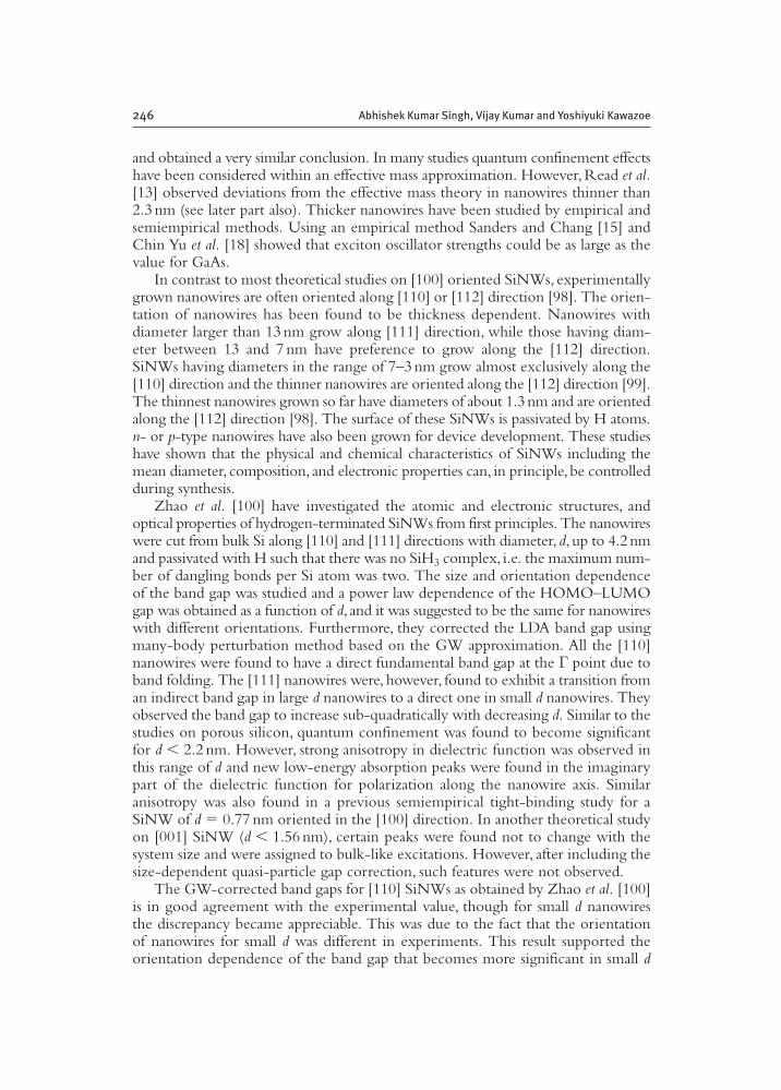
Very recently Singh et al. [96] have performed ab initio calculations on pristineSiNWs oriented along the [110] direction and showed them to be indirect band-gapsemiconductors. The nanowires were cut from bulk silicon in a rectangular shape andwere bounded by two {100} and two {110} facets in lateral directions (Fig. 6.14).They considered large unit cells with 12 or more layers of Si along the nanowire axisto allow for possible reconstructions on the surface and eliminate artifacts of periodicboundary conditions. In this family of SiNWs, the initial structure of a thin SiNWhad an array of Si atoms with three dangling bonds due to the presence of {100}facets and the way the facets meet at the edges. Consequently, this nanowire under-went severe reconstruction, strongly driven by the tendency of Si atoms to reduce thenumber of dangling bonds at the surface (Fig. 6.14). Such severe reconstructions ofvery thin SiNWs could change their overall structure. However, the important aspects
240 Abhishek Kumar Singh, Vijay Kumar and Yoshiyuki Kawazoe
c2c
(a) (b)
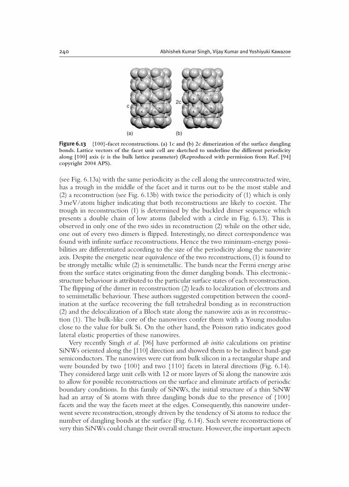
Figure 6.13 {100}-facet reconstructions. (a) 1c and (b) 2c dimerization of the surface danglingbonds. Lattice vectors of the facet unit cell are sketched to underline the different periodicityalong [100] axis (c is the bulk lattice parameter) (Reproduced with permission from Ref. [94]copyright 2004 APS).
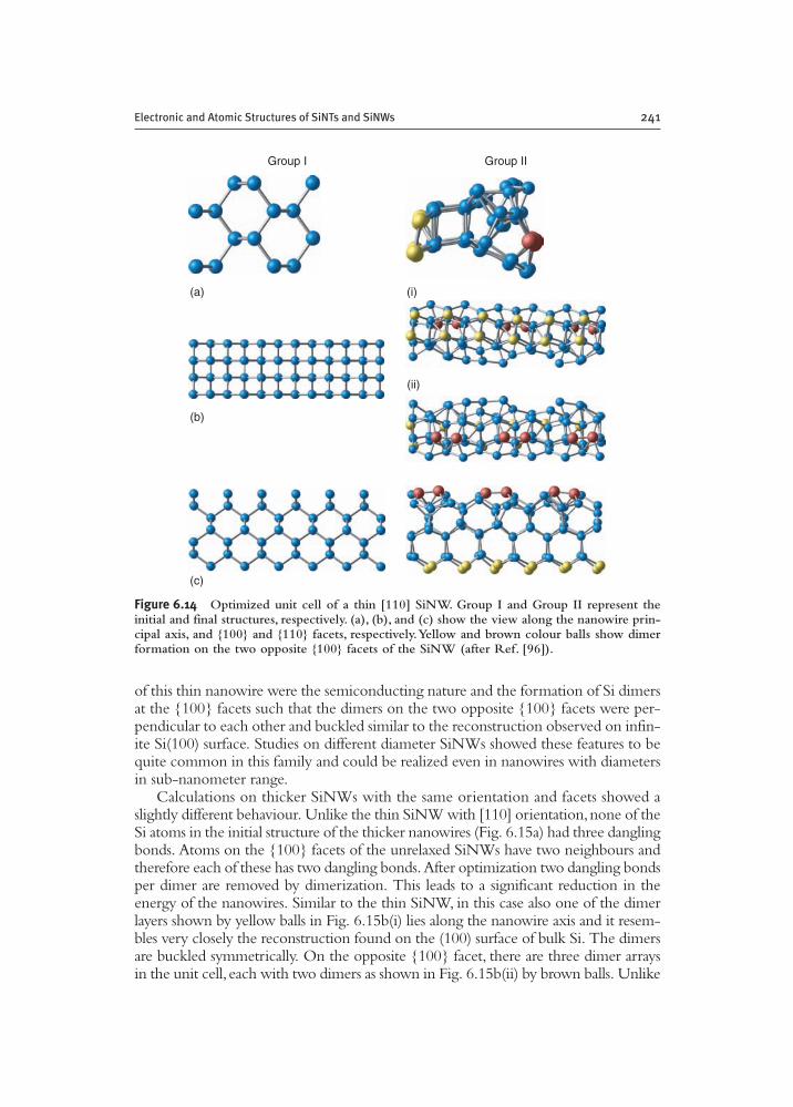
of this thin nanowire were the semiconducting nature and the formation of Si dimersat the {100} facets such that the dimers on the two opposite {100} facets were per-pendicular to each other and buckled similar to the reconstruction observed on infin-ite Si(100) surface. Studies on different diameter SiNWs showed these features to bequite common in this family and could be realized even in nanowires with diametersin sub-nanometer range.
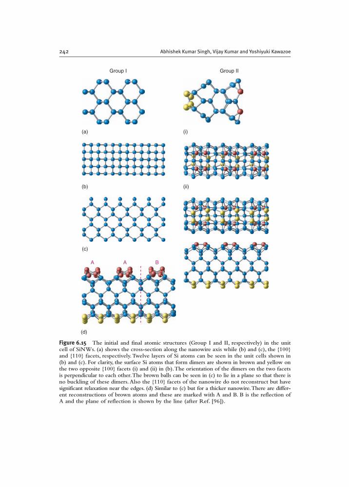
Calculations on thicker SiNWs with the same orientation and facets showed aslightly different behaviour. Unlike the thin SiNW with [110] orientation,none of theSi atoms in the initial structure of the thicker nanowires (Fig. 6.15a) had three danglingbonds. Atoms on the {100} facets of the unrelaxed SiNWs have two neighbours andtherefore each of these has two dangling bonds. After optimization two dangling bondsper dimer are removed by dimerization. This leads to a significant reduction in theenergy of the nanowires. Similar to the thin SiNW, in this case also one of the dimerlayers shown by yellow balls in Fig. 6.15b(i) lies along the nanowire axis and it resem-bles very closely the reconstruction found on the (100) surface of bulk Si. The dimersare buckled symmetrically. On the opposite {100} facet, there are three dimer arraysin the unit cell, each with two dimers as shown in Fig. 6.15b(ii) by brown balls. Unlike
Electronic and Atomic Structures of SiNTs and SiNWs 241
(i)
(ii)
(b)
(a)
(c)
Group I Group II
Figure 6.14 Optimized unit cell of a thin [110] SiNW. Group I and Group II represent theinitial and final structures, respectively. (a), (b), and (c) show the view along the nanowire prin-cipal axis, and {100} and {110} facets, respectively.Yellow and brown colour balls show dimerformation on the two opposite {100} facets of the SiNW (after Ref. [96]).
242 Abhishek Kumar Singh, Vijay Kumar and Yoshiyuki Kawazoe
Group IIGroup I
(i)(a)
(b)
(c)
BAA
(d)
(ii)
Figure 6.15 The initial and final atomic structures (Group I and II, respectively) in the unitcell of SiNWs. (a) shows the cross-section along the nanowire axis while (b) and (c), the {100}and {110} facets, respectively.Twelve layers of Si atoms can be seen in the unit cells shown in(b) and (c). For clarity, the surface Si atoms that form dimers are shown in brown and yellow onthe two opposite {100} facets (i) and (ii) in (b).The orientation of the dimers on the two facetsis perpendicular to each other.The brown balls can be seen in (c) to lie in a plane so that there isno buckling of these dimers.Also the {110} facets of the nanowire do not reconstruct but havesignificant relaxation near the edges. (d) Similar to (c) but for a thicker nanowire.There are differ-ent reconstructions of brown atoms and these are marked with A and B. B is the reflection ofA and the plane of reflection is shown by the line (after Ref. [96]).
bulk surfaces, these dimer arrays do not have an infinite extent and are terminated atthe edges of the nanowire. The pair of Si atoms forming a dimer on this face makes anadditional bond with the Si atom in the adjacent {110} facet. This way the remainingdangling bonds on the dimer atoms are weakened and it lowers the energy further.Consequently, the dimers are not buckled and remain planar (see Fig. 6.15c). The{110} facets,however,do not reconstruct but relaxation occurs which is more signifi-cant for the edge atoms. It is partly due to the fact that most of the atoms on thesefacets are already tricoordinated and any additional bond formation requires largestrain energy that is not compensated by the bond formation energy. The optimizedstructure showed the unit cell to consist of four Si layers along the nanowire axis.
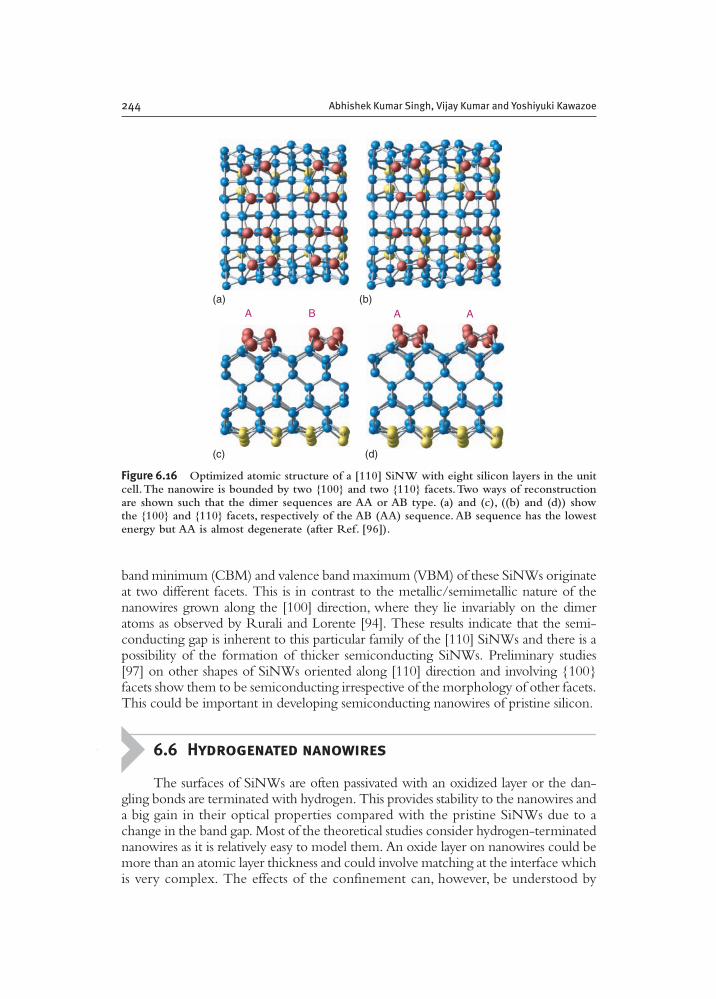
With increasing thickness of the SiNWs, the number of dimers in an array per-pendicular to the nanowire axis on a {100} facet increases to four or more (Fig. 6.15d)and this leads to buckling of the dimers on this face as well (Fig. 6.15d ) and an expan-sion in the mean diameter of the nanowires. The dimers that are in the middle of thesearrays are tricoordinated and the Si atoms in the core of the nanowires are tetracoor-dinated as in bulk. This leads to buckling features similar to infinite surfaces. Also theedge dimers are tricoordinated and buckled with slightly longer (2.42Å) bond lengthsas compared to the value (2.34Å) for the two inner dimers. These results showed thatthe atomic structure of thick SiNWs is not significantly affected by edges. The effectsof terminating the facets are more and more localized on the edges and elsewhere thereconstruction resembles one of the low energy reconstructions observed on the (100)surface of bulk Si. However,an interesting finding was the occurrence of two consecu-tive arrays of dimers (marked A and B in Fig. 6.15d) on a {100} facet that had mirrorsymmetry in a plane perpendicular to the axis of the nanowire. Further calculations[96] on nanowires with eight Si layers in a unit cell with two different configurations(i) having two dimer arrays with a reflection symmetry (Fig. 6.16a and c) and (ii) hav-ing two dimer arrays with similar consecutive arrangements (Fig. 6.16b and d), showedthem to be nearly degenerate in energy, though in the case (i) the energy was 0.04eVlower than the value for the case (ii). Therefore, a possibility of polytypism in thegrowth of these nanowires with different sequences of A and B type blocks of layerswas suggested. Interestingly, in all the cases, the nanowires were found to be semicon-ducting with nearly the same value of the band gap. Therefore, such a polytypism willnot affect the properties of SiNWs significantly.
6.5.3 Band Structure of SiNWs
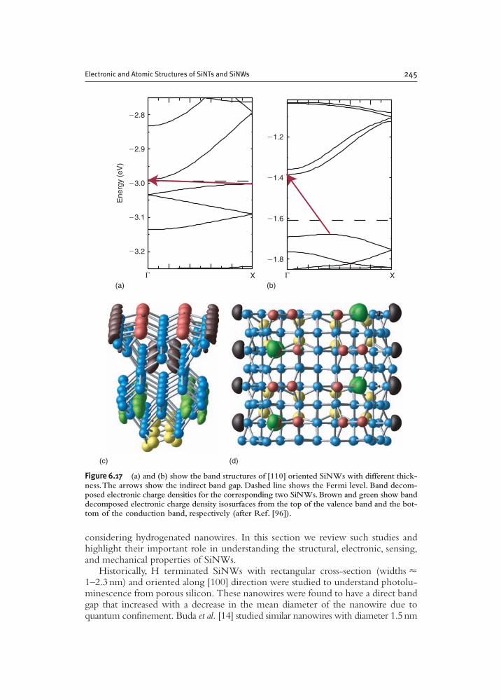
The band structures of the [110] SiNWs show that the nanowires are indirect band-gap semiconductors (Fig. 6.17a and b). The electronic charge density in Fig. 6.17cshows that the topmost valence band originates from sp3 type orbitals on the edgeatoms. The lobes pointing outside of the surface have large separation (3.77 and3.83Å) along the nanowire axis and overlap weakly. This leads to a relatively flat band.The electronic charge density from the bottom of the conduction band states comesfrom pz type orbitals on atoms in the nearly flat facets (Fig. 6.17c). The bonding withinsuch facets can be described in terms of sp2 type orbitals. The separations between thelobes of pz type orbitals are 3.69 and 3.92Å. Therefore, again the dispersion of the cor-responding band is small and the band is narrow. Similar results have been obtained forthicker nanowires. It is to be noted that the bands corresponding to the conduction
Electronic and Atomic Structures of SiNTs and SiNWs 243
band minimum (CBM) and valence band maximum (VBM) of these SiNWs originateat two different facets. This is in contrast to the metallic/semimetallic nature of thenanowires grown along the [100] direction, where they lie invariably on the dimeratoms as observed by Rurali and Lorente [94]. These results indicate that the semi-conducting gap is inherent to this particular family of the [110] SiNWs and there is apossibility of the formation of thicker semiconducting SiNWs. Preliminary studies[97] on other shapes of SiNWs oriented along [110] direction and involving {100}facets show them to be semiconducting irrespective of the morphology of other facets.This could be important in developing semiconducting nanowires of pristine silicon.
6.6 Hydrogenated nanowires
The surfaces of SiNWs are often passivated with an oxidized layer or the dan-gling bonds are terminated with hydrogen. This provides stability to the nanowires and a big gain in their optical properties compared with the pristine SiNWs due to achange in the band gap. Most of the theoretical studies consider hydrogen-terminatednanowires as it is relatively easy to model them. An oxide layer on nanowires could bemore than an atomic layer thickness and could involve matching at the interface whichis very complex. The effects of the confinement can, however, be understood by
244 Abhishek Kumar Singh, Vijay Kumar and Yoshiyuki Kawazoe
(a) (b)
(c) (d)
A B A A
Figure 6.16 Optimized atomic structure of a [110] SiNW with eight silicon layers in the unitcell.The nanowire is bounded by two {100} and two {110} facets.Two ways of reconstructionare shown such that the dimer sequences are AA or AB type. (a) and (c), ((b) and (d)) showthe {100} and {110} facets, respectively of the AB (AA) sequence.AB sequence has the lowestenergy but AA is almost degenerate (after Ref. [96]).
considering hydrogenated nanowires. In this section we review such studies andhighlight their important role in understanding the structural, electronic, sensing,and mechanical properties of SiNWs.
Historically, H terminated SiNWs with rectangular cross-section (widths �1–2.3 nm) and oriented along [100] direction were studied to understand photolu-minescence from porous silicon. These nanowires were found to have a direct bandgap that increased with a decrease in the mean diameter of the nanowire due toquantum confinement. Buda et al. [14] studied similar nanowires with diameter 1.5nm
Electronic and Atomic Structures of SiNTs and SiNWs 245
(d)(c)
�2.8
�2.9
�3.1
�3.0
�3.2
Ene
rgy
(eV
)
XΓ(a)
�1.2
�1.4
�1.8
�1.6
XΓ(b)
Figure 6.17 (a) and (b) show the band structures of [110] oriented SiNWs with different thick-ness.The arrows show the indirect band gap. Dashed line shows the Fermi level. Band decom-posed electronic charge densities for the corresponding two SiNWs.Brown and green show banddecomposed electronic charge density isosurfaces from the top of the valence band and the bot-tom of the conduction band, respectively (after Ref. [96]).
and obtained a very similar conclusion. In many studies quantum confinement effectshave been considered within an effective mass approximation. However, Read et al.[13] observed deviations from the effective mass theory in nanowires thinner than2.3 nm (see later part also). Thicker nanowires have been studied by empirical andsemiempirical methods. Using an empirical method Sanders and Chang [15] andChin Yu et al. [18] showed that exciton oscillator strengths could be as large as thevalue for GaAs.
In contrast to most theoretical studies on [100] oriented SiNWs, experimentallygrown nanowires are often oriented along [110] or [112] direction [98]. The orien-tation of nanowires has been found to be thickness dependent. Nanowires withdiameter larger than 13 nm grow along [111] direction, while those having diam-eter between 13 and 7 nm have preference to grow along the [112] direction.SiNWs having diameters in the range of 7–3 nm grow almost exclusively along the[110] direction and the thinner nanowires are oriented along the [112] direction [99].The thinnest nanowires grown so far have diameters of about 1.3nm and are orientedalong the [112] direction [98]. The surface of these SiNWs is passivated by H atoms.n- or p-type nanowires have also been grown for device development. These studieshave shown that the physical and chemical characteristics of SiNWs including themean diameter, composition, and electronic properties can, in principle, be controlledduring synthesis.
Zhao et al. [100] have investigated the atomic and electronic structures, andoptical properties of hydrogen-terminated SiNWs from first principles. The nanowireswere cut from bulk Si along [110] and [111] directions with diameter,d, up to 4.2nmand passivated with H such that there was no SiH3 complex, i.e. the maximum num-ber of dangling bonds per Si atom was two. The size and orientation dependenceof the band gap was studied and a power law dependence of the HOMO–LUMOgap was obtained as a function of d, and it was suggested to be the same for nanowireswith different orientations. Furthermore, they corrected the LDA band gap usingmany-body perturbation method based on the GW approximation. All the [110]nanowires were found to have a direct fundamental band gap at the Γ point due toband folding. The [111] nanowires were, however, found to exhibit a transition froman indirect band gap in large d nanowires to a direct one in small d nanowires. Theyobserved the band gap to increase sub-quadratically with decreasing d. Similar to thestudies on porous silicon, quantum confinement was found to become significantfor d � 2.2 nm. However, strong anisotropy in dielectric function was observed inthis range of d and new low-energy absorption peaks were found in the imaginarypart of the dielectric function for polarization along the nanowire axis. Similaranisotropy was also found in a previous semiempirical tight-binding study for aSiNW of d � 0.77 nm oriented in the [100] direction. In another theoretical studyon [001] SiNW (d � 1.56 nm), certain peaks were found not to change with thesystem size and were assigned to bulk-like excitations. However, after including thesize-dependent quasi-particle gap correction, such features were not observed.
The GW-corrected band gaps for [110] SiNWs as obtained by Zhao et al. [100]is in good agreement with the experimental value, though for small d nanowires the discrepancy became appreciable. This was due to the fact that the orientationof nanowires for small d was different in experiments. This result supported the orientation dependence of the band gap that becomes more significant in small d
246 Abhishek Kumar Singh, Vijay Kumar and Yoshiyuki Kawazoe
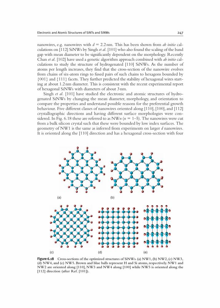
nanowires, e.g. nanowires with d � 2.2nm. This has been shown from ab initio cal-culations on [112] SiNWs by Singh et al. [101] who also found the scaling of the bandgap with mean diameter to be significantly dependent on the morphology. RecentlyChan et al. [102] have used a genetic algorithm approach combined with ab initio cal-culations to study the structure of hydrogenated [110] SiNWs. As the number ofatoms per length increases, they find that the cross-section of the nanowire evolvesfrom chains of six-atom rings to fused pairs of such chains to hexagons bounded by{001} and {111} facets. They further predicted the stability of hexagonal wires start-ing at about 1.2nm diameter. This is consistent with the recent experimental reportof hexagonal SiNWs with diameters of about 3nm.
Singh et al. [101] have studied the electronic and atomic structures of hydro-genated SiNWs by changing the mean diameter, morphology, and orientation tocompare the properties and understand possible reasons for the preferential growthbehaviour. Five different classes of nanowires oriented along [110], [100], and [112]crystallographic directions and having different surface morphologies were con-sidered. In Fig. 6.18 these are referred to as NWn (n � 1–5). The nanowires were cutfrom a bulk silicon crystal such that these were bounded by low index surfaces. Thegeometry of NW1 is the same as inferred from experiments on larger d nanowires.It is oriented along the [110] direction and has a hexagonal cross-section with four
Electronic and Atomic Structures of SiNTs and SiNWs 247
(a) (b)
(c) (d) (e)
Figure 6.18 Cross-sections of the optimized structures of SiNWs. (a) NW1, (b) NW2, (c) NW3,(d) NW4, and (e) NW5. Brown and blue balls represent H and Si atoms, respectively. NW1 andNW2 are oriented along [110], NW3 and NW4 along [100] while NW5 is oriented along the[112] direction (after Ref. [101]).
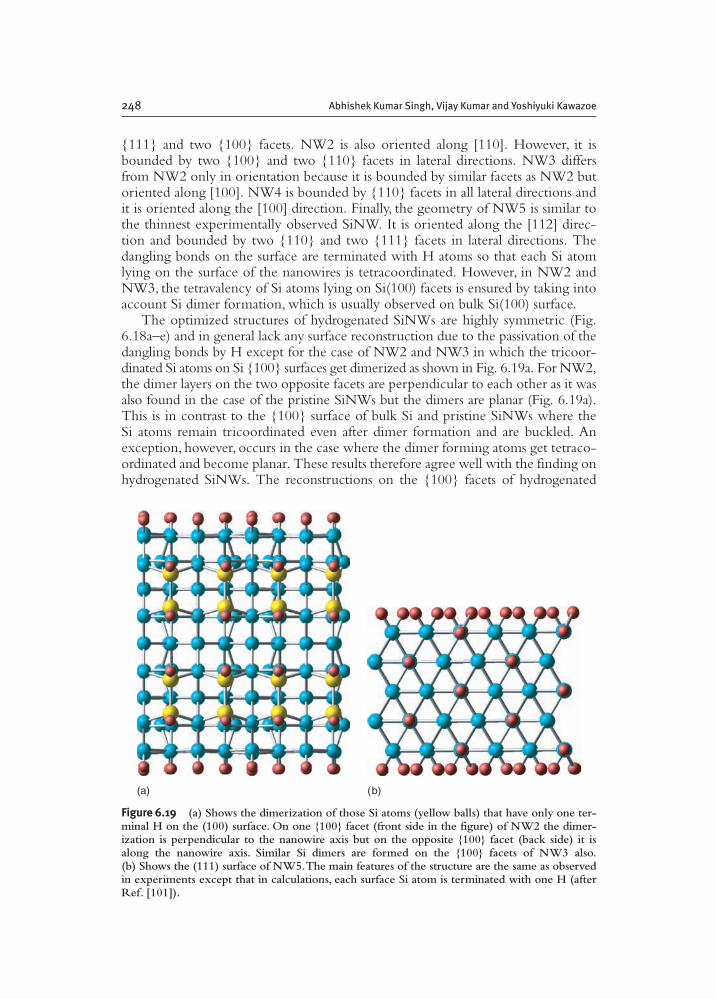
{111} and two {100} facets. NW2 is also oriented along [110]. However, it isbounded by two {100} and two {110} facets in lateral directions. NW3 differsfrom NW2 only in orientation because it is bounded by similar facets as NW2 butoriented along [100]. NW4 is bounded by {110} facets in all lateral directions andit is oriented along the [100] direction. Finally, the geometry of NW5 is similar tothe thinnest experimentally observed SiNW. It is oriented along the [112] direc-tion and bounded by two {110} and two {111} facets in lateral directions. Thedangling bonds on the surface are terminated with H atoms so that each Si atomlying on the surface of the nanowires is tetracoordinated. However, in NW2 andNW3, the tetravalency of Si atoms lying on Si(100) facets is ensured by taking intoaccount Si dimer formation, which is usually observed on bulk Si(100) surface.
The optimized structures of hydrogenated SiNWs are highly symmetric (Fig.6.18a–e) and in general lack any surface reconstruction due to the passivation of thedangling bonds by H except for the case of NW2 and NW3 in which the tricoor-dinated Si atoms on Si {100} surfaces get dimerized as shown in Fig. 6.19a. For NW2,the dimer layers on the two opposite facets are perpendicular to each other as it wasalso found in the case of the pristine SiNWs but the dimers are planar (Fig. 6.19a).This is in contrast to the {100} surface of bulk Si and pristine SiNWs where the Si atoms remain tricoordinated even after dimer formation and are buckled. Anexception, however, occurs in the case where the dimer forming atoms get tetraco-ordinated and become planar. These results therefore agree well with the finding onhydrogenated SiNWs. The reconstructions on the {100} facets of hydrogenated
248 Abhishek Kumar Singh, Vijay Kumar and Yoshiyuki Kawazoe
(a) (b)
Figure 6.19 (a) Shows the dimerization of those Si atoms (yellow balls) that have only one ter-minal H on the (100) surface. On one {100} facet (front side in the figure) of NW2 the dimer-ization is perpendicular to the nanowire axis but on the opposite {100} facet (back side) it isalong the nanowire axis. Similar Si dimers are formed on the {100} facets of NW3 also.(b) Shows the (111) surface of NW5.The main features of the structure are the same as observedin experiments except that in calculations, each surface Si atom is terminated with one H (afterRef. [101]).
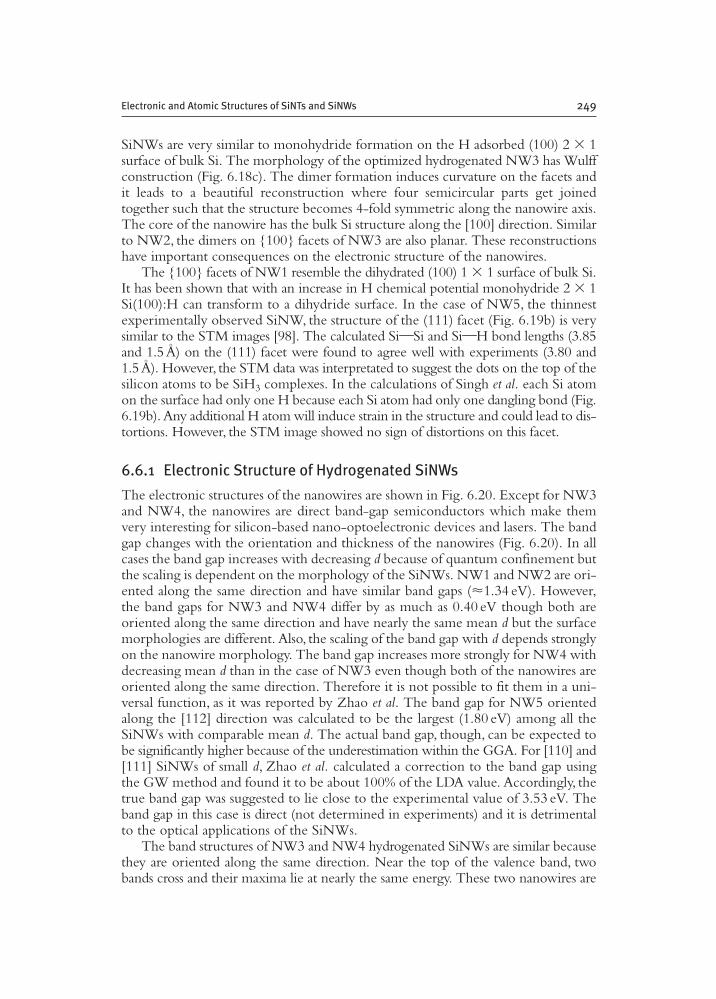
SiNWs are very similar to monohydride formation on the H adsorbed (100) 2 � 1surface of bulk Si. The morphology of the optimized hydrogenated NW3 has Wulffconstruction (Fig. 6.18c). The dimer formation induces curvature on the facets andit leads to a beautiful reconstruction where four semicircular parts get joinedtogether such that the structure becomes 4-fold symmetric along the nanowire axis.The core of the nanowire has the bulk Si structure along the [100] direction. Similarto NW2, the dimers on {100} facets of NW3 are also planar. These reconstructionshave important consequences on the electronic structure of the nanowires.
The {100} facets of NW1 resemble the dihydrated (100) 1 � 1 surface of bulk Si.It has been shown that with an increase in H chemical potential monohydride 2 � 1Si(100):H can transform to a dihydride surface. In the case of NW5, the thinnestexperimentally observed SiNW, the structure of the (111) facet (Fig. 6.19b) is verysimilar to the STM images [98]. The calculated Si!Si and Si!H bond lengths (3.85and 1.5Å) on the (111) facet were found to agree well with experiments (3.80 and1.5Å). However, the STM data was interpretated to suggest the dots on the top of thesilicon atoms to be SiH3 complexes. In the calculations of Singh et al. each Si atomon the surface had only one H because each Si atom had only one dangling bond (Fig.6.19b). Any additional H atom will induce strain in the structure and could lead to dis-tortions. However, the STM image showed no sign of distortions on this facet.
6.6.1 Electronic Structure of Hydrogenated SiNWs
The electronic structures of the nanowires are shown in Fig. 6.20. Except for NW3and NW4, the nanowires are direct band-gap semiconductors which make themvery interesting for silicon-based nano-optoelectronic devices and lasers. The bandgap changes with the orientation and thickness of the nanowires (Fig. 6.20). In allcases the band gap increases with decreasing d because of quantum confinement butthe scaling is dependent on the morphology of the SiNWs. NW1 and NW2 are ori-ented along the same direction and have similar band gaps (�1.34 eV). However,the band gaps for NW3 and NW4 differ by as much as 0.40 eV though both areoriented along the same direction and have nearly the same mean d but the surfacemorphologies are different. Also, the scaling of the band gap with d depends stronglyon the nanowire morphology. The band gap increases more strongly for NW4 withdecreasing mean d than in the case of NW3 even though both of the nanowires areoriented along the same direction. Therefore it is not possible to fit them in a uni-versal function, as it was reported by Zhao et al. The band gap for NW5 orientedalong the [112] direction was calculated to be the largest (1.80 eV) among all theSiNWs with comparable mean d. The actual band gap, though, can be expected tobe significantly higher because of the underestimation within the GGA. For [110] and[111] SiNWs of small d, Zhao et al. calculated a correction to the band gap usingthe GW method and found it to be about 100% of the LDA value. Accordingly, thetrue band gap was suggested to lie close to the experimental value of 3.53 eV. Theband gap in this case is direct (not determined in experiments) and it is detrimentalto the optical applications of the SiNWs.
The band structures of NW3 and NW4 hydrogenated SiNWs are similar becausethey are oriented along the same direction. Near the top of the valence band, twobands cross and their maxima lie at nearly the same energy. These two nanowires are
Electronic and Atomic Structures of SiNTs and SiNWs 249
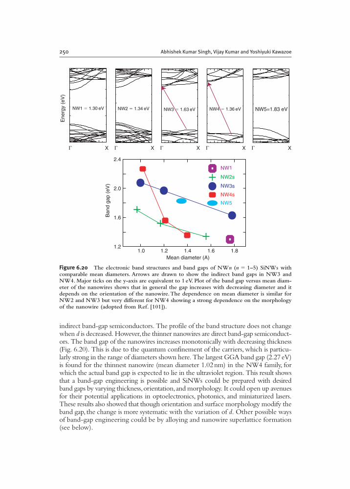
indirect band-gap semiconductors. The profile of the band structure does not changewhen d is decreased. However, the thinner nanowires are direct band-gap semiconduct-ors. The band gap of the nanowires increases monotonically with decreasing thickness(Fig. 6.20). This is due to the quantum confinement of the carriers, which is particu-larly strong in the range of diameters shown here. The largest GGA band gap (2.27eV)is found for the thinnest nanowire (mean diameter 1.02nm) in the NW4 family, forwhich the actual band gap is expected to lie in the ultraviolet region. This result showsthat a band-gap engineering is possible and SiNWs could be prepared with desiredband gaps by varying thickness,orientation,and morphology. It could open up avenuesfor their potential applications in optoelectronics, photonics, and miniaturized lasers.These results also showed that though orientation and surface morphology modify theband gap, the change is more systematic with the variation of d. Other possible waysof band-gap engineering could be by alloying and nanowire superlattice formation(see below).
250 Abhishek Kumar Singh, Vijay Kumar and Yoshiyuki Kawazoe
1.2
1.6
2.0
2.4
1.0 1.2 1.4 1.6 1.8
NW4s
NW2s
NW3s
NW1
NW5
Ban
d ga
p (e
V)
Mean diameter (A)
Ene
rgy
(eV
)
XΓ XΓ XΓ XΓXΓ
NW1 � 1.30 eV NW2 � 1.34 eV NW5=1.83 eVNW4 � 1.36 eVNW3 � 1.63 eV
Figure 6.20 The electronic band structures and band gaps of NWn (n � 1–5) SiNWs withcomparable mean diameters. Arrows are drawn to show the indirect band gaps in NW3 andNW4. Major ticks on the y-axis are equivalent to 1 eV. Plot of the band gap versus mean diam-eter of the nanowires shows that in general the gap increases with decreasing diameter and itdepends on the orientation of the nanowire.The dependence on mean diameter is similar forNW2 and NW3 but very different for NW4 showing a strong dependence on the morphologyof the nanowire (adopted from Ref. [101]).
6.6.2 Effects of Doping and H Defects
Besides optical applications, SiNWs have been shown to hold great promise for label-free detection of biological and chemical species [30–34]. The electrical detectionof species by SiNW sensors is based on the principle of solid-state field effect transis-tor (FET) in which p- or n-doped nanowires are used and the gating is achievedchemically by a change in the surface charge when a species binds on the surface lead-ing to a change in the conductance. For the detection of specific biological molecules,the surface of SiNWs in such devices is modified by attaching receptors that bindselectively the species to be detected. In another setup the surface of a SiNW wasmodified for measuring pH so that it could undergo protonation and deprotonation.Such a change in the surface charge gates the nanowire without applying any voltageand again a change in conductance could be used for detection. In contrast to bulksurfaces where the changes in the electronic structure are confined to the surface, theeffects of receptor-legend chemistry on the surface of a nanowire go deeper into thecore of the nanowire and this further increases the sensitivity of the sensors to the pointof single molecule detection. Unlike oxidized nanowires where the layers of silica aregenerally thick, the surfaces of hydrogenated nanowires have only one layer of H topacify the dangling bonds. Therefore, surfaces of hydrogenated nanowires could beeven more sensitive and any changes in surface chemistry could have a pronouncedeffect on the sensing capability of nanowires. A variation in hydrogen concentrationon the surface could affect the sensing capabilities of different surface morphologiesand the associated surface reconstructions. On {100} facets deficiency of H was foundto lead to dimer formation and therefore H deficiency does not have a strong effect.However, on other facets deficiency of H leads to states which appear in the band gap.Any attachment to such sites can affect the transport properties very significantly. Singhet al. studied the effects of changing the concentration of H on the surface of NW4SiNWs because they involve only {110} facets. Removal of one H atom from each ofthe corner Si atoms of the NW4 nanowire (8H atom/unit cell) has an effect of creat-ing unpaired electrons on the surface which leads to a drastic change in the band struc-ture (Fig. 6.21). The electronic states associated with defects have energies lying withinthe band gap and it leads to a dramatic reduction in the band gap of the SiNWs. Theorigin of the defect states is seen from the charge density arising from the defect states(inset in Fig. 6.21). It is seen that the charge densities arising from the VBM and CBMare strongly localized on the eight corner Si atoms, showing clearly that these bandsoriginate from hydrogen defect sites. Importantly, these sites can act as centres of attrac-tion for various receptors. In contrast to this result, it is found that SiNWs with {100}facets can easily offset the effects of H deficit on the surface by dimerization as we dis-cussed in the case of NW2 and NW3 earlier. Therefore,on such surfaces the band gapand electronic properties are unlikely to be affected by H defects. On the other handnanowires with {110} or {111} facets could be ideal for sensors because their elec-tronic properties could be modified drastically by changing H concentration.
Most of the electronic or sensing applications of SiNWs have been shown for p-or n-doped nanowires having thicknesses in the range of 10–30nm and with oxidizedlayers on the surface. With the development of hydrogenated thin SiNWs, it isimportant to know the effects of doping on the electronic structure of such nanowires.Since there are significant differences in the electronic properties of NW1 and NW4,
Electronic and Atomic Structures of SiNTs and SiNWs 251
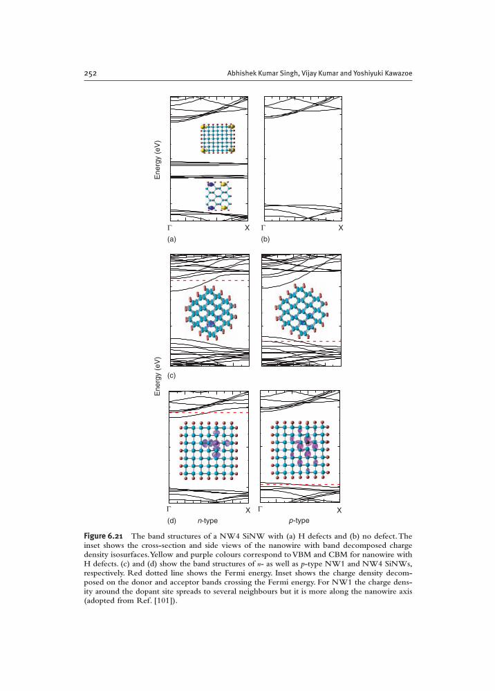
252 Abhishek Kumar Singh, Vijay Kumar and Yoshiyuki Kawazoe
Ene
rgy
(eV
)E
nerg
y (e
V)
XΓ XΓ(a) (b)
(c)
(d)XΓ XΓ
n-type p-type
Figure 6.21 The band structures of a NW4 SiNW with (a) H defects and (b) no defect.Theinset shows the cross-section and side views of the nanowire with band decomposed chargedensity isosurfaces.Yellow and purple colours correspond to VBM and CBM for nanowire withH defects. (c) and (d) show the band structures of n- as well as p-type NW1 and NW4 SiNWs,respectively. Red dotted line shows the Fermi energy. Inset shows the charge density decom-posed on the donor and acceptor bands crossing the Fermi energy. For NW1 the charge dens-ity around the dopant site spreads to several neighbours but it is more along the nanowire axis(adopted from Ref. [101]).
Singh et al. considered these as prototypes to study the effects of doping. Boron andphosphorous atoms were doped to study p- and n-type SiNWs, respectively. Afteroptimization, the band structures of the doped nanowires showed (Fig. 6.21) a shift ofthe Fermi level towards the valence and conduction band for p- and n-type SiNW,respectively. This behaviour is quite universal and is observed in both types ofnanowires (Fig. 6.21) irrespective of their orientation and surface morphology.However, few subtle differences were observed that arise not because of doping butbecause of the difference in the surface morphologies of the nanowires. For exam-ple, the dispersion in the valence band of p-NW1 is more than that in the case ofp-NW4, implying heavier holes in p-NW4 in comparison to p-NW1. Likewise,better conduction properties are expected in p-NW1. A comparison of the bandstructures of the doped and undoped nanowires (Figs. 6.20 and 6.21) shows that thedispersion of the conduction or valance bands does not change much upon doping.However, the band structure of the nanowires could be tailored by growing them indifferent orientations and with different surface morphologies. This could be used todesign doped SiNWs with better conduction properties.
The doping concentrations in these doped SiNWs correspond to a case of heavydoping as one dopant in the unit cell represents about 0.4% dopant concentration.The band structures show that the Fermi level lies in the acceptor (donor) bands forthe p- (n-) type nanowires. The electronic charge density decomposed on CBM forthe n-type and VBM for the p-type nanowires shows that these bands originate fromthe dopant sites. For the p-type nanowire the electronic charge extends up to 3rdand 4th nearest neighbours and it can be expected even for lower doping concen-trations a similar effect would be observed. It can enhance the sensing capabilities ofthin nanowires further. Therefore, thin hydrogenated SiNWs could have potential forsilicon-based device development at the smallest scale.
Conductance of cluster assembled short SiNWs passivated by H and connectedto aluminium electrodes has been studied from DFT calculations [103]. The short(�0.6nm) nanowires were found to be fully metallized due to the metal-induced gapstates while longer (2.5nm) nanowires form a nanoscale Schottky barrier with heightslarger than the bulk value by 40–90%. Using ab initio calculations,Durandurdu [104].very recently also predicted a stable small diameter SiNW. The wire is constructedfrom expanded phases of silicon namely clathrate Si34 and Si46 structures, and foundthese to be energetically more favourable than the diamond type nanowires with thesame diameters. Furthermore, the wires are semiconducting with the band-gap energyof 0.22 and 0.34eV.
6.7 Nanowire superlattices
Apart from the n- and p- type materials the other important component of thesemiconductor industry which is most often used to bring the versatilities in electronicand photonic properties of devices are compositionally modulated structures, whichare also known as superlattices. Nanowire-based superlattices are quite promising toachieve bulk-like functionalities at the nanoscale. Nanowire superlattices from GroupIII–V,II–VI and Group IV materials have already been synthesized [105–107]. Besides,superlattices another way to develop variation in the properties is by preparing
Electronic and Atomic Structures of SiNTs and SiNWs 253
core-shell heterostructures. These can be formed by growing crystalline overlayerson nanocrystals or nanowires and offer enhanced emission efficiency [108].
Planar modulations in nanowires have been developed mostly for the III–V orII–VI materials to have variations in optical properties which are interesting in barcoding. Some of the experimental developments could be found in Chapter Five byZhou et al. However, modulation of the radial composition has received much lessattention until recently. Lauhon et al. [109] have recently synthesized SiGe core-shellnanowires. Such nanowires are quite thick and are difficult to model by first princi-ples calculations within the current available resources. However, peculiarities ofstructural and electronic properties of large core-shell nanowires can be understoodby studying thin nanowires or atleast a trend could be found which can be appliedto larger diameter nanowires. Mustin and Wang have recently carried out a detailedfirst-principles DFT study of the composition dependence of the structural and elec-tronic properties of the core-shell type SiGe nanowire heterostructures [110]. Theyanalysed the relationship between structural characteristics and chemical compositionin these core-shell structured systems and obtained a quantitative estimation of thedegree of deviation from the linearity assumed by the Vegard’s law [111] which statesthat the relaxed lattice parameter of a two component system is a linear function ofthe composition. The analysis of the changes in the local and global geometry andelectronic structure of the epitaxial SiGe hydrogen-passivated core-shell structurednanowires revealed strong core-specific features for both the structural and electronicproperties. They also observed the existence of both negative and positive deviationsfrom the linear behaviour of the calculated structural parameters of the nanowireswith the tensile strained Si core and compressive strained Ge core, respectively. Theyfurther observed [109] direct-to-indirect transition for the fundamental band gap inGe-core/Si-shell nanowires. Based on the weak size dependence of the critical com-position for direct-to-indirect gap transition they suggested [109] Ge-core/Si-shellnanowires with 5 and 15nm shell diameter to have direct and indirect fundamentalgaps, respectively. A smooth synthesis process could be expected by adding Ge shellonto Si core, as the calculation indicated a gradual increase in the tensile strain,whereas the strain relaxation for compressively strained Ge cores is much involved[109]. They observed direct band-gap practically over the whole compositionalrange for Si-core/Ge-shell nanowire heterostructures. This along with the possibil-ity of the band-gap variation with change in composition, diameter of nanowire,and/or shell thickness suggests a promising perspective for band-gap engineeringand the fabrication of novel nanoarchitectures for optoelectronic applications.Theoretical studies on this technologically important aspect of nanowires are still ina very nascent stage and demands for more involved studies which can include pla-nar modulated superstructure.
6.8 Conclusion and perspective remarks
The developments and achievements in the field of synthesis and applications ofthe Si nanowires have brought them as strongest candidates in the arena of ever evolv-ing area of nanotechnology. They have emerged as most important and smallest circuitelements for electronic applications as well as the smallest and precise sensors for the
254 Abhishek Kumar Singh, Vijay Kumar and Yoshiyuki Kawazoe
detection of chemical and biological species at molecular scale. The possibilities offorming nanotubular structures of silicon with metal encapsulation have open up novelpossibilities of quasi-one-dimensional structures of silicon which could be bothmetallic and semiconducting. A long-standing goal of the integration of electronicwith optoelectronic in silicon-based devices appears to be realizable for the first timein nanosilicon-based devices. Theoretical studies are giving way to develop a micro-scopic understanding of the properties of such nanostructures of silicon and arecomplimenting experimental studies as often at this scale a detailed knowledge ofstructure from experiments is difficult. This is one of the research areas where com-plimentary theoretical and experimental research can be helpful in atomic scaledesign of silicon nanostructures. The full potentials of SiNW and nanotube appli-cations are yet to be unfolded and we expect to see many developments and rapidprogress both theoretically and experimentally in the years to come.
Acknowledgements
We thankfully acknowledge the support of the staff of the Center forComputational Material Science, IMR, Tohoku University for allowing the use ofthe Hitachi SR8000/64 supercomputing facilities. AKS is thankful for the supportof a JSPS fellowship. AKS also thankfully acknowledges partial support of theMRSEC Program of the National Science Foundation under Award No. DMR05-20415. VK gratefully acknowledges support at RICS from NAREGI Nano ScienceProject, Ministry of Education, Culture, Sports, Science and Technology, Japan andthe hospitality at IMR, Tohoku University, RICS, AIST and the Institute ofMathematical Sciences.
REFERENCES
1. A.G. Cullis and L.T. Canham, Nature 353, 335 (1991).2. S. Iijima, Nature 354, 56 (1991).3. W. Liang, et al., Nature 411, 665 (2001).4. S.P. Franh, P. Poncharal, Z.L. Wang and W.A. de Heer, Science 280, 1744 (1998).5. M.J. Biercuk, et al., Appl. Phys. Lett. 80, 2767 (2002).6. Y. Chen, et al., Appl. Phys. Lett. 78, 2128 (2001).7. A.C. Dillon and M.J. Heben, Appl. Phys. A. 72, 133 (2001).8. N.S. Lee, et al., Diamond Relat. Mater. 10, 265 (2001).9. H. Sugie, et al., Appl. Phys. Lett. 78, 2578 (2001).
10. P.G. Collins, K. Bradley, M. Ishigami and A. Zettel, Science 287, 1801 (2000).11. L. Guo, E. Leobandung and S. Chou, Science 275, 649 (1997).12. S. Tiwari, et al., Appl. Phys. Lett. 68, 1377 (1996).13. R.J. Read, et al., Phys. Rev. Lett. 69, 1232 (1992)14. F. Buda, J. Kohanoff and M. Parrinello, Phys. Rev. Lett. 69, 1272 (1992).15. G.D. Sanders and Y-C. Chang, Phys. Rev. B 45, 9202 (1992).16. M.S. Hybertsen and M. Needels, Phys. Rev. B 48, 4608 (1993).17. C. Delerue, G. Allan and M. Lannoo, Phys. Rev. B 48, 11024 (1993).18. C-Y. Yeh, S.B. Zhang and A. Zunger, Phys. Rev. B 50, 14405 (1994).19. B. Delley and E.F. Steigmeier, Appl. Phys. Lett. 67, 2370 (1995).20. J-B. Xia and K.W. Cheah, Phys. Rev. B 55, 15688 (1997).21. A.M. Morales and C.M. Lieber, Science 279, 208 (1998).
Electronic and Atomic Structures of SiNTs and SiNWs 255
22. J.D. Holmes, K.P. Johnston, R. Doty and B.A. Korgel, Science 287, 1471 (2000).23. V. Schmidt, S. Senz and U. Gosele, Nano Lett. 5, 931 (2005).24. Y. Wu, Y. Cui, L. Huynh, C.J. Barrelet, D.C. Bell and C.M. Lieber, Nano Lett. 4, 433 (2004).25. X.-Y. Zhang, et al., Adv. Mater. 13, 1238 (2001).26. S. Ge, et al., Adv. Mater. 17, 56 (2005).27. Z. Zhong, et al., Science 302, 1377 (2003).28. Y. Cui and C.M. Lieber, Science 291, 851 (2001).29. Y. Huang, X. Duan, Y. Cui, L.J. Lauhon, K.-H. Kim and C.M. Lieber, Science 294, 1313 (2001).30. Y. Cui, Q. Wei, H. Park and C.M. Lieber, Science 293, 1289 (2001).31. P. Alivisatos, Nat. Biotechnol. 22, 47 (2004).32. Z. Zheng, et al., Nat. Biotechnol. 23, 1294 (2005).33. J. Hahm and C.M. Lieber, Nano Lett. 4, 51 (2003).34. F. Patolsky, G. Zheng, O. Hayden, M. Lakadamyali, X. Zhuang and C.M. Lieber, Proc. Natl.Acad.
Sci. USA 101, 14017 (2004).35. U.W. Wang, C. Chen, K. Lin, Y. Fang and C.M. Lieber, Proc. Natl. Acad. Sci. USA 102, 3208
(2005).36. R.Q. Zhang, S.T. Lee, C.K. Law, W.K. Li and B.K. Teo, Chem. Phys. Lett. 364, 251 (2002).37. S.B. Fagan, et al., Phys. Rev. B 61, 9994 (2000).38. S.B. Fagan, R. Mota, R.J. Baierle, G. Paiva, A.J.R. da Silva and A. Fazzio, J. Mol. Struct.
(Theochem) 539, 101 (2001).39. A.S. Barnard and S.P. Russo, J. Phys. Chem. B 107, 7577–7581 (2003).40. S.Y. Jeong, J.Y. Kim, H.D. Yang, B.N. Yoon, S.H. Choi, S.J. Eum, C.W. Yang and Y.H. Lee, Adv.
Mater. 15, 1172 (2003).41. M. De Crescenzi, et al., Appl. Phys. Lett. 86, 23190 (2005).42. Y-W Chen, Y-H. Tang, L-Z. Pei and C. Guo, Adv. Mater. 15,1172–1176 (2003).43. V. Kumar and Y. Kawazoe, Phys. Rev. Lett. 87, 045503 (2001); ibid. 91 199901(E) (2003).44. V. Kumar and Y. Kawazoe, Phys. Rev. B 65, 073404 (2002).45. V. Kumar and Y. Kawazoe, Phys. Rev. Lett. 88, 235540 (2002).46. V. Kumar and Y. Kawazoe, Appl. Phys. Lett. 86, 859 (2002).47. H. Hiura, T. Miyazaki and T. Kanayama, Phys. Rev. Lett. 86, 1733 (2002).48. V. Kumar, C. Majumder and Y. Kawazoe, Chem. Phys. Lett. 363, 319 (2002).49. V. Kumar, Eur. Phys. J. D 24, 227 (2003).50. A.K. Singh, V. Kumar and Y. Kawazoe, Phys. Rev. B 71, 115429 (2005).51. M. Ohara, K. Koyasu,A. Nakajima and K. Kaya, Chem. Phys. Lett. 371, 490 (2003).52. K. Koyasu, M. Akutsu, M. Mitsui and A. Nakajima, JACS 127, 4998 (2005).53. A.K. Singh, V. Kumar, T.M. Briere and Y. Kawazoe, Nano Lett. 2, 1243 (2002).54. A.K. Singh, T.M. Briere, V. Kumar and Y. Kawazoe, Phys. Rev. Lett. 91 146802, (2003).55. M. Menon,A.N. Andriotis and G.E. Froudakis, Nano Lett. 2, 301 (2002).56. A.N. Andriotis, G. Mpourmpakis, G.E. Froudakis and M. Menon, New J. Phys. 4, 78 (2002).57. V. Kumar, T.M. Briere and Y. Kawazoe, Phys. Rev. B 68, 155412 (2003).58. W. Kohn and L. Sham, Phys. Rev. 140,A1133 (1965).59. J.P. Perdew, Electronic Structure of Solids ’91, Eds. P. Ziesche and H. Eschrig, (Akademie Verlag,
Berlin 1991); J.P. Perdew, S. Kurth, A. Zupan and P. Blaha, Phys. Rev. Lett. 82, 2544 (1999);J.F. Dobson and J. Wang, Phys. Rev. B 62, 10038 (2000).
60. G. Kresse and J. Furthmuller, Phys. Rev. B 54, 11169 (1996); Comput. Mater. Sci. 6, 15 (1996).61. G. Kresse and J. Joubert, Phys. Rev. B 59, 1758 (1999).62. G. Seifert, T. Kohler, H.M. Urbassek, E. Hernandez and T. Frauenheim, Phys. Rev. B 63, 193409
(2001).63. S. Gemming and G. Seifert, Phys. Rev. 68, 075416 (2003).64. G. Seifert and T. Frauenheim, J. Korean Phys. Soc. 37, 89 (2000).65. X. Yang and J. Ni, Phys. Rev. B 72, 195426 (2005).66. Y.H. Tang, L.Z. Pei, Y.W. Chen and C. Guo, Phys. Rev. Lett. 95, 116102 (2005).67. V. Kumar, Comp. Mater. Sci. 36, 1 (2006).68. A.K. Singh, V. Kumar and Y. Kawazoe, J. Mater. Chem. 14, 555 (2004).69. J.C. Grossman and L. Mitas, Phys. Rev. B 52, 16735 (1995).70. V. Kumar and Y. Kawazoe, Phys. Rev. Lett. 90, 055502 (2003).
256 Abhishek Kumar Singh, Vijay Kumar and Yoshiyuki Kawazoe
71. H. Vach and Q. Brulin, Phys. Rev. Lett. 95, 165502 (2005).72. A.A. Saranin, et al., Nano Lett. 4, 1469 (2004).73. A.K. Singh, Ph.D. Thesis, 2004.74. G. Mederios-Ribeiro,A.M. Bratkovski, T.I. Kamins, D.A.A. Ohlberg and R.S. Williams, Science
279, 353 (1998)20.75. C. Preinesberger, S.K. Becker, S. Vandr, T. Kalka and M. Dhne, J. Appl. Phys. 91, 1695 (2002).76. Y. Chen, D.A.A. Ohlberg, G. Mederios-Ribeiro, Y.A. Chang and R.S. Williams, Appl. Phys.
Lett. 76, 4004 (2000); Y. Chen, D.A.A. Ohlberg and R.S. Williams, J. Appl. Phys. 91, 3213(2002).
77. J. Nogami, B.Z. Liu, M.V. Katkov, C. Ohbuchi and N.O. Birge, Phys. Rev. B 63, 233305 (2001).78. T. Dumitric, M. Hua and B.I. Yakobson, Phys. Rev. 70, 241303 (2004).79. A.K. Singh, V. Kumar and Y. Kawazoe, Phys. Rev. B 69, 233406 (2004).80. V. Kumar and Y. Kawazoe, Appl. Phys. Lett. 83, 2677 (2003).81. Y.D. Park, et al., Science 295, 651 (2002).82. Y. Zhao, T. Shishidou and A.J. Freeman, Phys. Rev. Lett. 90, 47204 (2002).83. A.K. Singh, V. Kumar and Y. Kawazoe, Phys. Rev. B 71, 075312 (2005).84. A.K. Singh, V. Kumar and Y. Kawazoe, Eur. Phys. J. D 71, 075312 (2005).85. B. Marsn and K. Sattler, Phys. Rev. B 60, 11593 (1999).86. K. Ho,A.A. Shvartsburg, B. Pan, Z. Lu, C. Wang, J.G. Wacker, J.L. Fye and M.F. Jarrold, Nature
392, 582 (1998).87. L. Mitas, J.C. Grossman, I. Stich and J. Tobik, Phys. Rev. Lett. 84, 1479 (2000).88. U. Rothlisberger, W. Andreoni and M. Parrinello, Phys. Rev. Lett. 72, 665 (1994).89. B. Li, P. Cao, R.Q. Zeng and S.T. Lee, Phys. Rev. B 65, 125305 (2002).90. M. Menon and E. Richter, Phys. Rev. Lett. 91, 792 (1999).91. S. Ismail-Beigi and T. Arias, Phys. Rev. B 55, 11923 (1998).92. M.S. Hybertsen, M. Needels, N. Roberts and R.J. Needs, Surf. Sci. 236, 112 (1990); J. Fritsch
and P. Pavone, ibid. 344, 159 (1995).93. Y. Zhao and B.I. Yakobson, Phys. Rev. Lett. 83, 035501 (2003).94. R. Rurali and N. Lorente, Phys. Rev. Lett. 94, 026805 (2005).95. R. Rurali and N. Lorente, Nanotechnology 16, S250 (2005).96 A.K. Singh, V. Kumar, R. Note and Y. Kawazoe, Nano Lett. 5, 2302 (2005).97. A.K. Singh, V. Kumar and Y. Kawazoe, Unpublished.98. D.D.D. Ma, C.S. Lee, F.C.K. Au, S.Y. Tong and S.T. Lee, Science 299, 18742003 (2003).99. Y. Wu, Y. Cui, L. Huynh, C.J. Barrelet, D.C. Bell and C.M. Lieber, Nano Lett. 4, 433 (2004).
100. X. Zhao, C.M. Wei, L. Yang and M.Y. Chou, Phys. Rev. Lett. 92, 236805 (2004).101. A.K. Singh, V. Kumar, R. Note and Y. Kawazoe, Nano Lett. 6, 920(2006).102. T.-L. Chan, C.V. Ciobanu, F.-C. Chuang, N. Lu, C.-Z. Wang and K.-M. Ho, Nano Lett. 6, 277
(2006).103. U. Landman, R.N. Barnett,A.G. Scherbakov and P. Avouris, Phys. Rev. Lett. 85, 1958 (2000).104. M. Durandurdu, Phys. Stat. Sol. B 243, R7 (2006).105. M.S. Gudiksen, et al., Nature 415, 617 (2002).106. M.T. Bjork, et al., Appl. Phys. Lett. 80, 1058 (2002).107. Y.Y. Wu, R. Fan and P.D. Yang, Nano Lett. 2, 83 (2002).108. M. Nirmal and L. Brus, Acc. Chem. Res. 32, 407 (1999).109. L.J. Lauhon, et al., Nature 420, 57 (2002).110. R.N. Musin and Xiao-Qian Wang, Phy. Rev. B 71, 155318 (2005).111. L. Vegard, Z. Phys. 5, 17 (1921).
Electronic and Atomic Structures of SiNTs and SiNWs 257
Related Documents