2 nd Berkeley Symposium on Energy Efficient Electronic Systems The Path Toward Efficient Nano-Mechanical Circuits and Systems http://www.chi-yun.com/blog/wp-content/uploads/2008/10/ba-road-less.jp Tsu-Jae King Liu 1 Elad Alon 1 , Vladimir Stojanovic 2, Dejan Markovic 3 1 University of California at Berkeley 2 Massachusetts Institute of Technology 3 University of California at Los Angeles November 3, 2011

Welcome message from author
This document is posted to help you gain knowledge. Please leave a comment to let me know what you think about it! Share it to your friends and learn new things together.
Transcript

2nd Berkeley Symposium on Energy Efficient Electronic Systems
The Path Toward Efficient Nano-Mechanical Circuits
and Systemshttp://www.chi-yun.com/blog/wp-content/uploads/2008/10/ba-road-less.jp
Tsu-Jae King Liu1
Elad Alon1, Vladimir Stojanovic2, Dejan Markovic3
1University of California at Berkeley2Massachusetts Institute of Technology3University of California at Los Angeles
November 3, 2011

Source: ITU, Mark Lipacis, Morgan Stanley Research
http://www.morganstanley.com/institutional/techresearch/pdfs/2SETUP_12142009_RI.pdf
# D
EVIC
ES (M
M)
YEAR
Market Growth
Investment
Transistor Scaling
Higher Performance,Lower Cost
Proliferation of Electronic Devices
2

Infrastructionalcore
Sensory swarm(trillions of devices)
Vision for 2020: Swarms of Electronics
J. Rabaey, ASPDAC 2008 3
Driver for More of Moore’s Law
Driver for More Than Moore’s Law
Mobile access

Why Mechanical Switches?
• Relays have zero off-state leakage zero leakage energy
Source
DrainGate
Air gap
tgap tdimple
3-Terminal Switch
• Relays switch on/off abruptly allows for aggressive VDD scaling
(ultra-low dynamic energy)
1.E-14
1.E-12
1.E-10
1.E-08
1.E-06
1.E-04
Measured I-V
Gate Voltage
Dra
in C
urre
nt
S≈0.1mV/dec
VPIVRL
4
• Electro-Mechanical Relay Design for Digital ICs
• Relay-Based IC Design
• Relay Reliability
• Summary
Outline
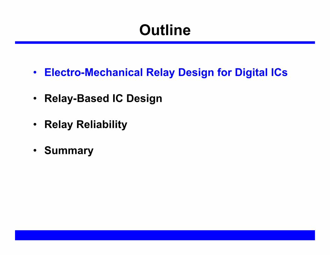
• A voltage is applied between the gate and body to bring the channel into contact with the source and drain. Folded-flexure design relieves residual stress. Gate oxide layer insulates the channel from the gate.
4-Terminal Relay Structure
Body
Drain
Source
Body
Gate
Channel
A
A’
Isometric View:
Drain Source
Gate
Body
GateOxide
substrate
IDS
insulator
AA’ cross-section: OFF state
AA’ cross-section: ON state
6R. Nathanael et al., IEDM 2009
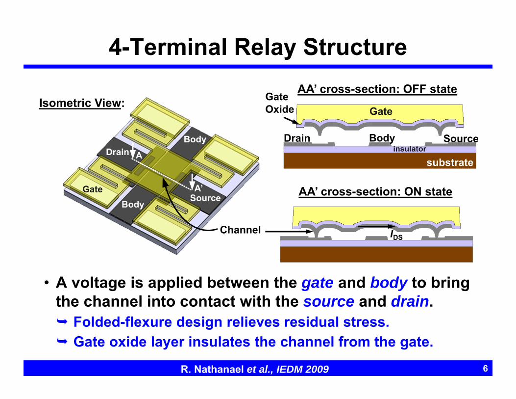
4-T Relay Process Flow (I)
100nm SiO2
80 nm Al2O3
50 nm W
Si substrate
200nm100nm
Deposit Al2O3 substrate insulator• ALD at 300oC
Deposit & pattern W electrodes• DC magnetron sputtering
Deposit 1st sacrificial LTO• LPCVD at 400oCDefine contact regions
Deposit 2nd sacrificial LTO
Deposit & pattern W channel
Deposit Al2O3 gate oxide
50 nm W
40 nm Al2O3
SiO2
Mask 1: Electrode
Mask 2: Contact dimple
Mask 3: Channel
7R. Nathanael et al., IEDM 2009
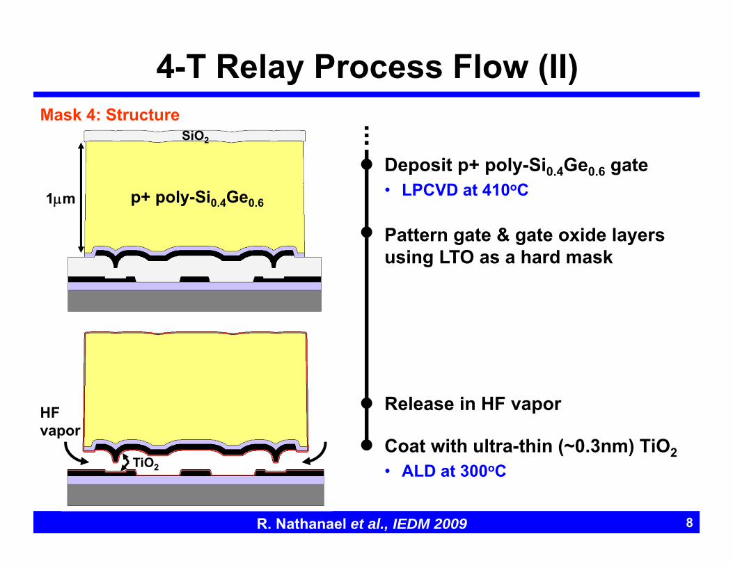
4-T Relay Process Flow (II)
8
TiO2
HFvapor
p+ poly-Si0.4Ge0.6
SiO2
1m
Deposit p+ poly-Si0.4Ge0.6 gate• LPCVD at 410oC
Coat with ultra-thin (~0.3nm) TiO2• ALD at 300oC
Pattern gate & gate oxide layers using LTO as a hard mask
Release in HF vapor
Mask 4: Structure
R. Nathanael et al., IEDM 2009
R. Nathanael et al., 2009 IEDM / V. Pott et al., Proc. IEEE, Vol. 98, pp. 2076-2094, 2010
4-T Relay ID-VG Characteristic
• Zero IOFF; S < 0.1 mV/dec• Hysteresis is due to pull-in mode operation (tdimple > tgap/3)
and surface adhesion.
Plan View SEM of 4-T Relay
20 μm
9
1E-14
1E-12
1E-10
1E-08
1E-06
1E-04
1E-02
0 2 4 6 8 10
I DS(A
)
VGS (V)
VD = 2VVS = 0V
VB = 0VVB = –9V
(a)
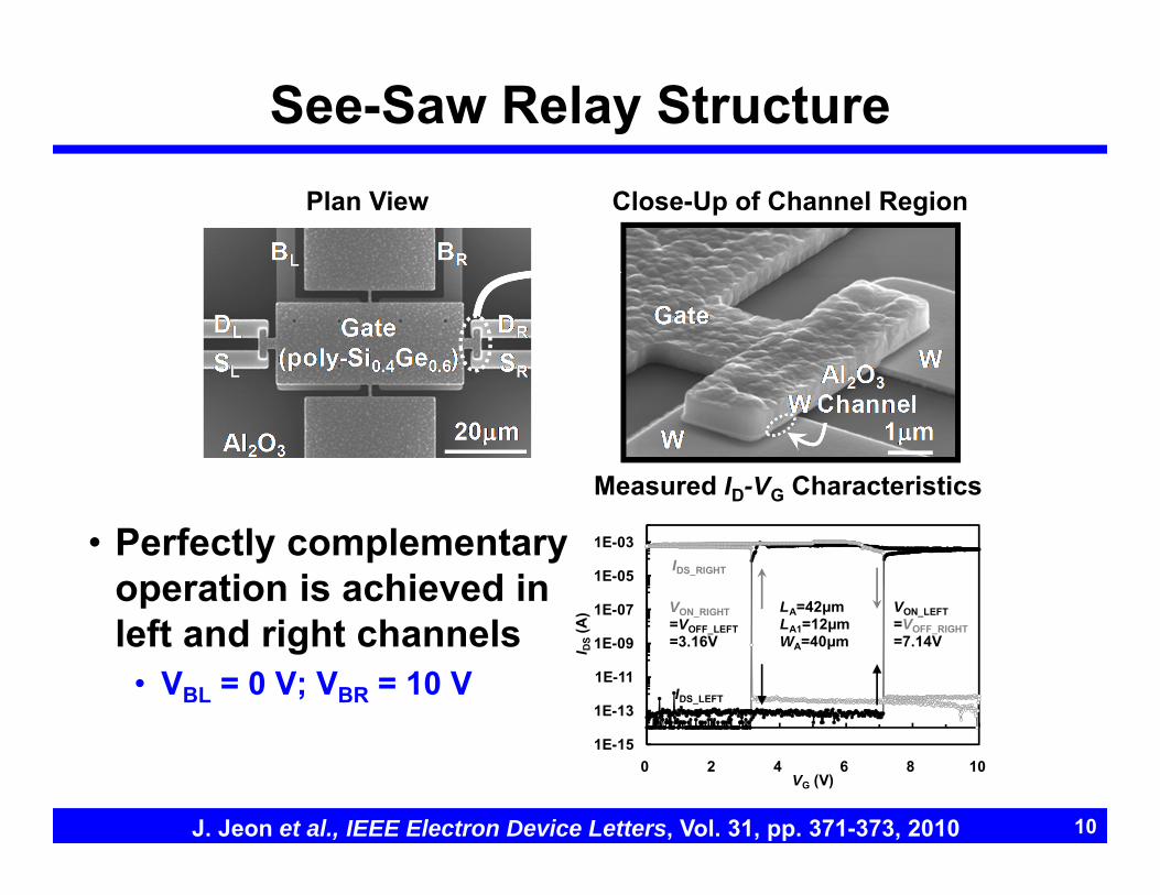
• Perfectly complementary operation is achieved in left and right channels
• VBL = 0 V; VBR = 10 V
Plan View Close-Up of Channel Region
See-Saw Relay Structure
Measured ID-VG Characteristics
1E-15
1E-13
1E-11
1E-09
1E-07
1E-05
1E-03
0 2 4 6 8 10
I DS
(A)
VG (V)
IDS_RIGHT
IDS_LEFT
VON_LEFT=VOFF_RIGHT=7.14V
VON_RIGHT=VOFF_LEFT=3.16V
LA=42μmLA1=12μmWA=40μm
J. Jeon et al., IEEE Electron Device Letters, Vol. 31, pp. 371-373, 2010 10

See-Saw Relay Latch
SRAM Cell VCTRL
VDATANMOS
G
DRDL
SRSL
BRBL
VSN
VWL
VBL
Seesaw
VDD
GND
NMOSStorage Node
Demonstrated SRAM Cell Operation
0
6
12
VW
L (V
)0
6
12
VD
ATA
(V)
0
6
12
0 5 10 15 20 25Time (s)
VB
L (V)
0
6
12V
CTR
L (V)
R = READW = WRITE (b-a)
(b-c)
(b-d)
W '0'
R '0' R '1' R '1'R '0'
W '0' W '1' W '1'
(b-b)
V DD=12V
11J. Jeon et al., IEEE/ASME J. MicroElectroMechanical Systems, Vol. 19, pp. 1012-1014, 2010.
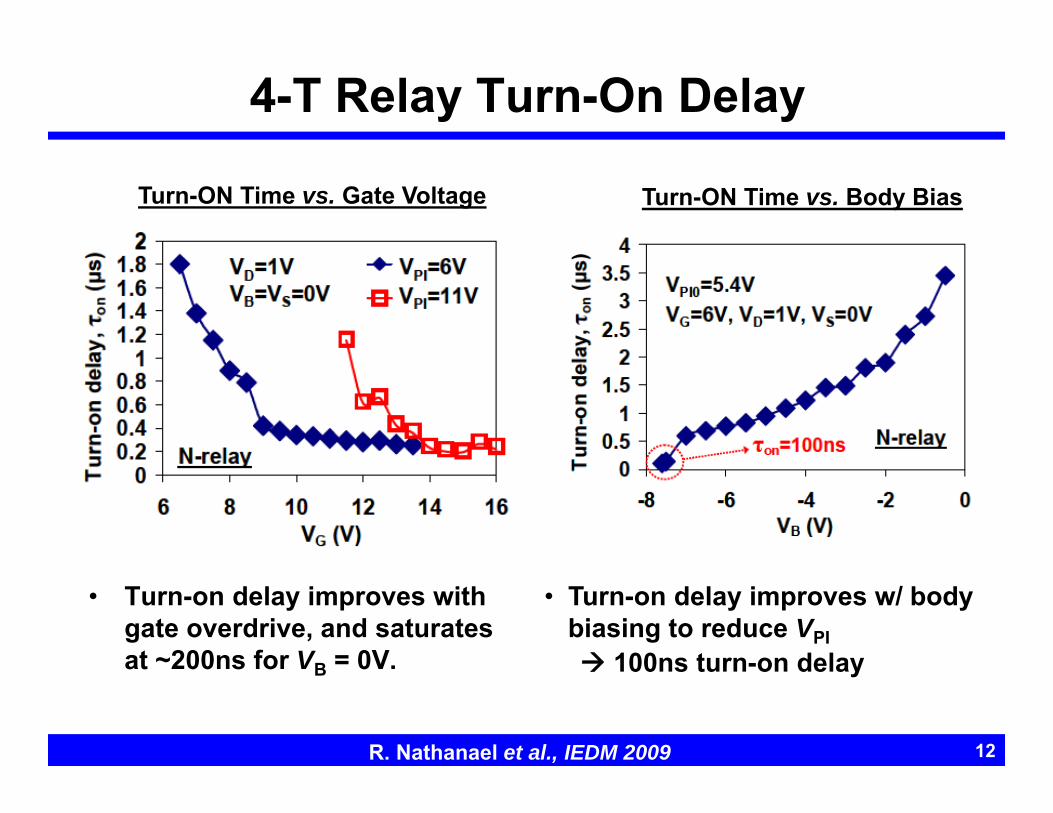
4-T Relay Turn-On Delay
• Turn-on delay improves with gate overdrive, and saturates at ~200ns for VB = 0V.
Turn-ON Time vs. Gate Voltage Turn-ON Time vs. Body Bias
• Turn-on delay improves w/ body biasing to reduce VPI 100ns turn-on delay
12R. Nathanael et al., IEDM 2009
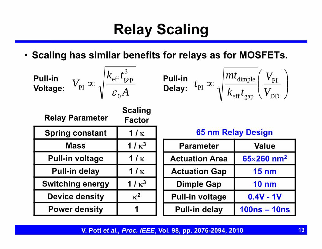
, , Relay Scaling• Scaling has similar benefits for relays as for MOSFETs.
65 nm Relay DesignSpring constant 1 / Mass 1 / 3
Pull-in voltage 1 / Pull-in delay 1 /
Switching energy 1 / 3
Device density 2
Power density 1
Relay ParameterScalingFactor
V. Pott et al., Proc. IEEE, Vol. 98, pp. 2076-2094, 2010
Pull-inVoltage:
Pull-inDelay:
Parameter ValueActuation Area 65260 nm2
Actuation Gap 15 nmDimple Gap 10 nm
Pull-in voltage 0.4V - 1VPull-in delay 100ns – 10ns
Atk
V0
3gapeff
PI
DD
PI
gapeff
dimplePI V
Vtk
mtt
13

• Electro-Mechanical Relay Design for Digital ICs
• Relay-Based IC Design
• Relay Reliability
• Summary
Outline
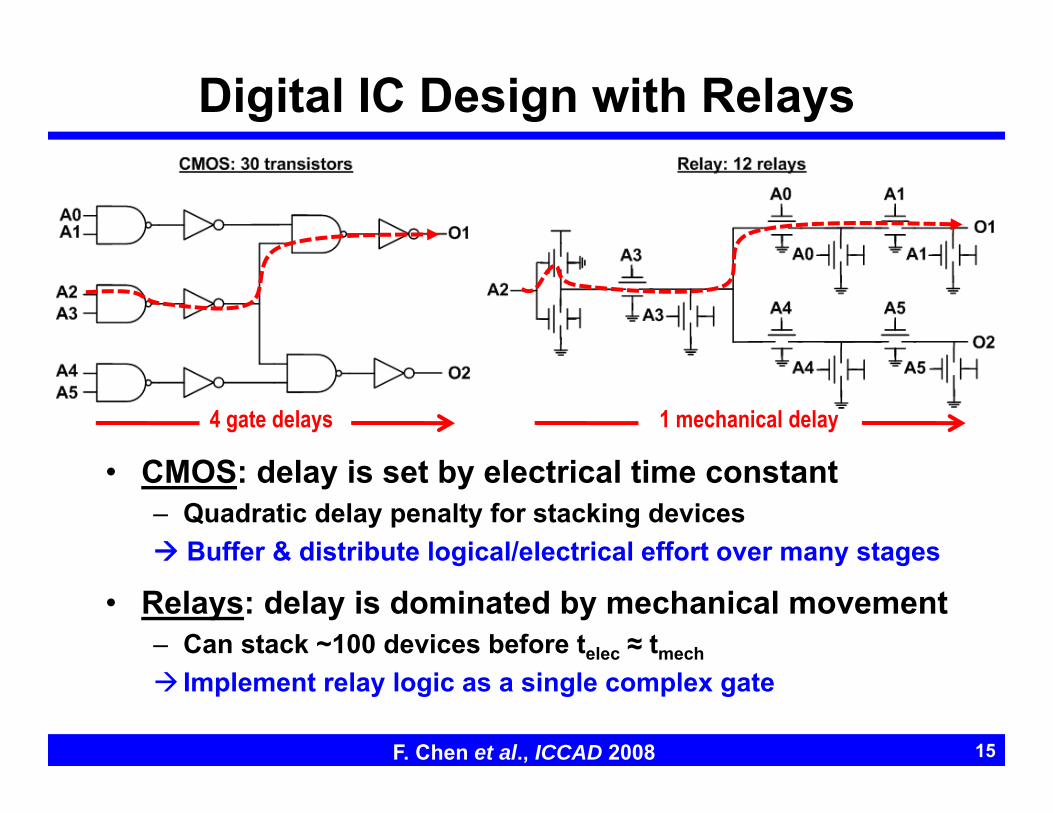
4 gate delays 1 mechanical delay
Digital IC Design with Relays
F. Chen et al., ICCAD 2008
• CMOS: delay is set by electrical time constant‒ Quadratic delay penalty for stacking devices Buffer & distribute logical/electrical effort over many stages
• Relays: delay is dominated by mechanical movement‒ Can stack ~100 devices before telec ≈ tmech
Implement relay logic as a single complex gate
15
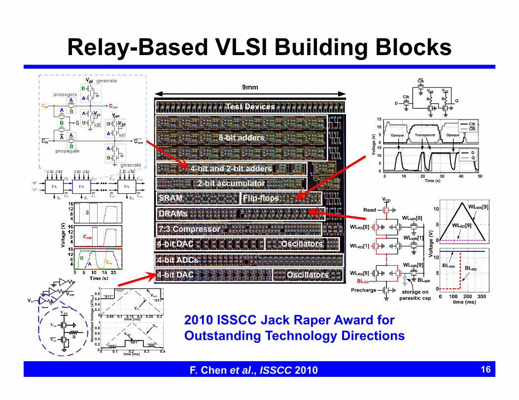
Relay-Based VLSI Building Blocks
2010 ISSCC Jack Raper Award for Outstanding Technology Directions
F. Chen et al., ISSCC 2010 16

Technology Transfer to SEMATECH
1st prototype: 120 µm x 150 µm Scaled relay: 20 µm x 20 µm
SEMATECH: 0.25 µm lithoUC Berkeley: 1 µm litho
17

Energy-Delay Comparison with CMOS
transition probability=0.01cap/CMOS inverter=0.57fF
• Scaled relay technology is projected to provide for >10x energy savings, at clock rates up to ~100MHz
V. Pott et al., Proc. IEEE, Vol. 98, pp. 2076-2094, 2010 18
0 V
Vdd
OutputInput
30-stage FO4 inverter chain:
0 V
VddOutput
30-relay chain:
CMOS
65 nm technology
• Electro-Mechanical Relay Design for Digital ICs
• Relay-Based IC Design
• Relay Reliability
• Summary
Outline
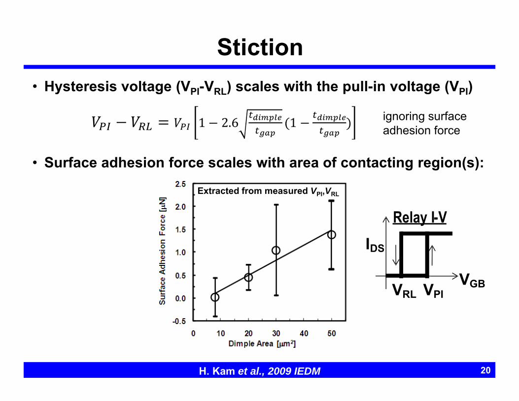
• Hysteresis voltage (VPI-VRL) scales with the pull-in voltage (VPI)
• Surface adhesion force scales with area of contacting region(s):
ignoring surface adhesion force
Extracted from measured VPI,VRL
Stiction
H. Kam et al., 2009 IEDM 20
VGB
IDS
VPIVRL
Relay I-V
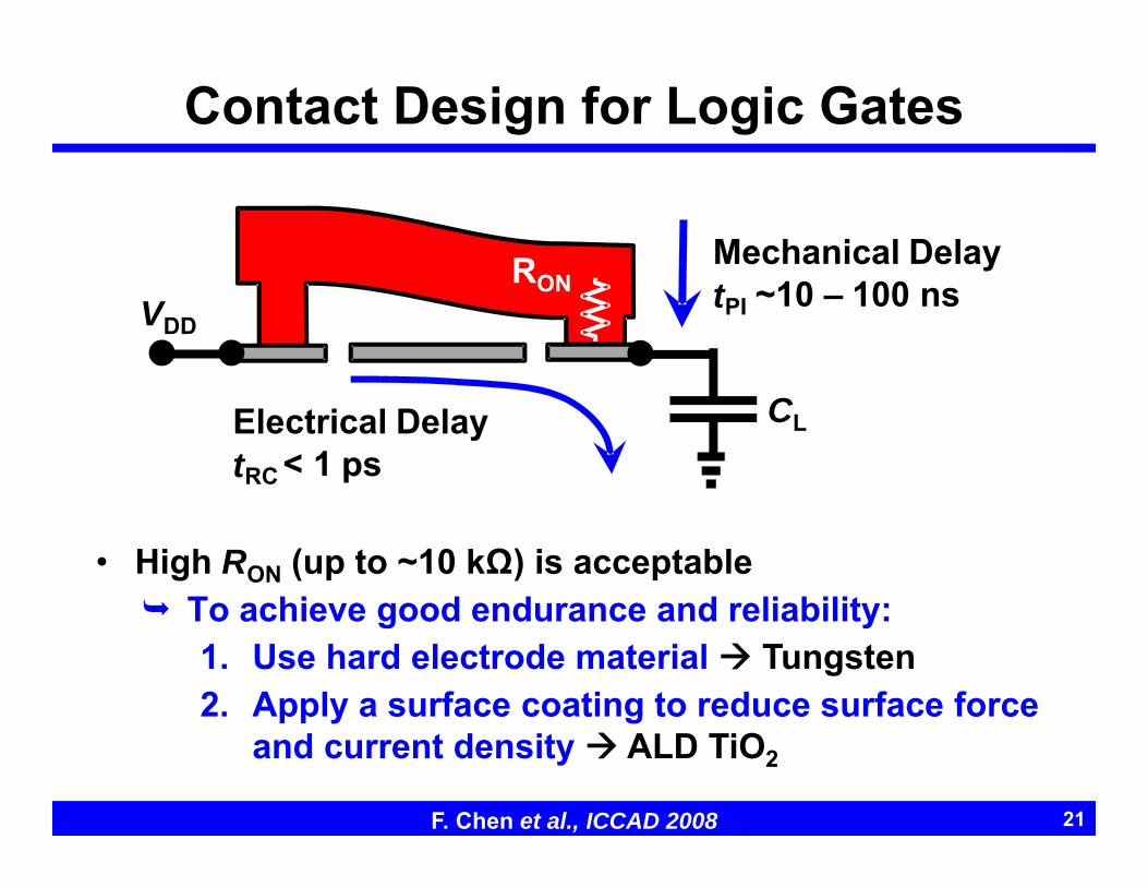
Contact Design for Logic Gates
• High RON (up to ~10 kΩ) is acceptable To achieve good endurance and reliability:
1. Use hard electrode material Tungsten2. Apply a surface coating to reduce surface force
and current density ALD TiO2
VDD
Electrical DelaytRC < 1 ps
Mechanical DelaytPI ~10 – 100 nsRON
21F. Chen et al., ICCAD 2008
CL
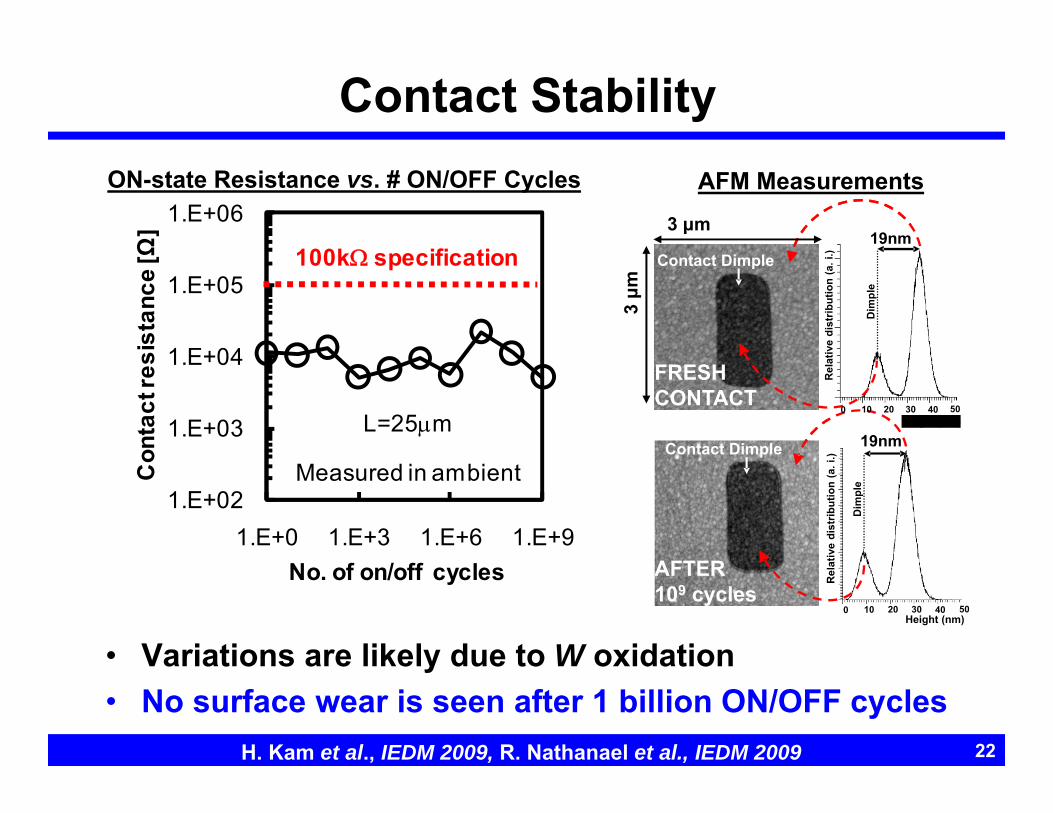
Contact Stability
• Variations are likely due to W oxidation• No surface wear is seen after 1 billion ON/OFF cycles
ON-state Resistance vs. # ON/OFF Cycles AFM Measurements
Never tested
Dimple
Rel
ativ
e di
strib
utio
n (a
. i.)
19nm
Dim
ple
(a) (b)
Rel
ativ
e di
strib
utio
n (a
. i.)
0 10 20 30 40 50
0 10 20 30 40 50
Height (nm)
Height (nm)
19nm
Dim
ple
(c) (d)
FRESH CONTACT
Contact Dimple
Rel
ativ
e di
strib
utio
n (a
. i.)
19nm
Dim
ple
Rel
ativ
e di
strib
utio
n (a
. i.)
0 10 20 30 40 50
0 10 20 30 40 50
Height (nm)
Height (nm)
Dim
ple
AFTER 109 cycles
Contact Dimple
3 μm
3 μm
19nm
1.E+02
1.E+03
1.E+04
1.E+05
1.E+06
1.E+0 1.E+3 1.E+6 1.E+9No. of on/off cycles
Con
tact
resi
stan
ce [Ω
]
100k specification
L=25m
Measured in ambient
H. Kam et al., IEDM 2009, R. Nathanael et al., IEDM 2009 22
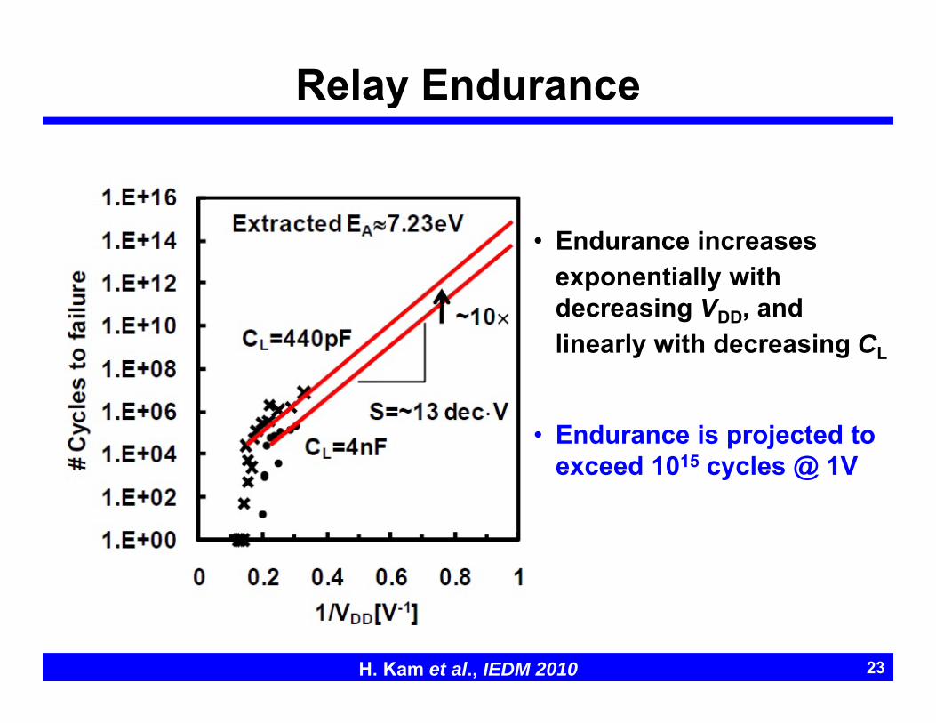
Relay Endurance
• Endurance increases exponentially with decreasing VDD, and linearly with decreasing CL
• Endurance is projected to exceed 1015 cycles @ 1V
H. Kam et al., IEDM 2010 23
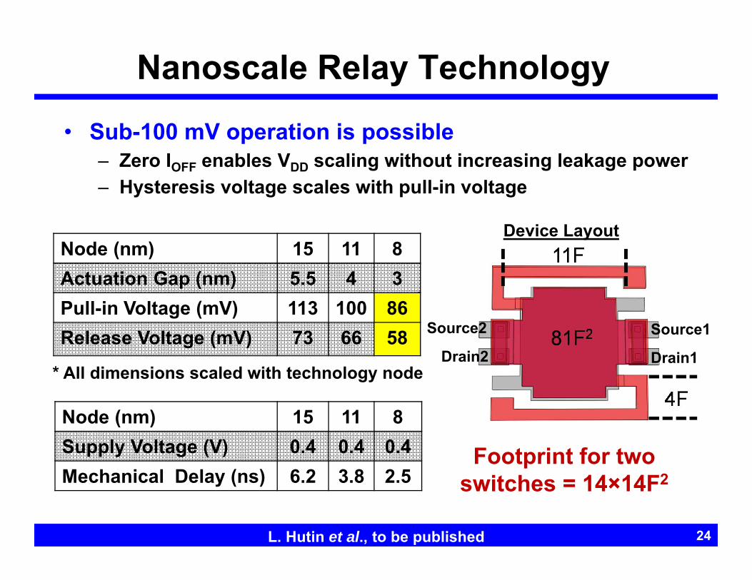
Nanoscale Relay Technology
• Sub-100 mV operation is possible‒ Zero IOFF enables VDD scaling without increasing leakage power‒ Hysteresis voltage scales with pull-in voltage
24
Node (nm) 15 11 8Actuation Gap (nm) 5.5 4 3Pull-in Voltage (mV) 113 100 86Release Voltage (mV) 73 66 58
* All dimensions scaled with technology node
Footprint for two switches = 14×14F2
Node (nm) 15 11 8Supply Voltage (V) 0.4 0.4 0.4Mechanical Delay (ns) 6.2 3.8 2.5
L. Hutin et al., to be published
Source1
Drain1
Source2
Drain2
Device Layout
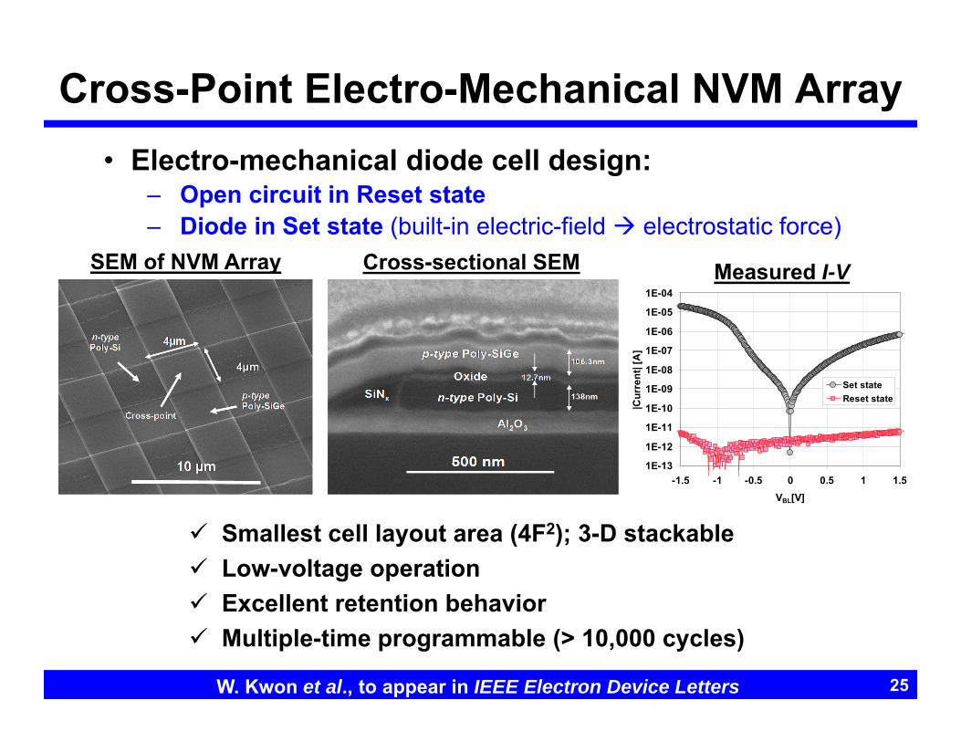
Cross-Point Electro-Mechanical NVM Array
Smallest cell layout area (4F2); 3-D stackable Low-voltage operation Excellent retention behavior Multiple-time programmable (> 10,000 cycles)
25W. Kwon et al., to appear in IEEE Electron Device Letters
1E-13
1E-12
1E-11
1E-10
1E-09
1E-08
1E-07
1E-06
1E-05
1E-04
-1.5 -1 -0.5 0 0.5 1 1.5VBL[V]
|Cur
rent
| [A
]
Set stateReset state
• Electro-mechanical diode cell design:‒ Open circuit in Reset state‒ Diode in Set state (built-in electric-field electrostatic force)
Measured I-VCross-sectional SEMSEM of NVM Array
• Electro-Mechanical Relay Design for Digital ICs
• Relay-Based IC Design
• Relay Reliability
• Summary
Outline

Summary
• Mechanical switches have the ideal properties of zero off-state leakage and abrupt turn-on/turn-off. potential for achieving very low E/op (<1 aJ)
• Dimensional scaling is required to achieve low-voltage operation and adequate reliability ‒ VDD < 100 mV‒ endurance > 1015 cyclesMaterials optimization can yield further improvements.
• New circuit and system architectures are needed to fully realize the potential energy-efficiency benefits. device and circuit design co-optimization is key!
27

Acknowledgements• NEM-Relay Team (current and former) members:
Post-docs: Louis Hutin; Hei Kam (now with Intel);Vincent Pott (now with IME, Singapore)
Students: Rhesa Nathanael, Jaeseok Jeon (now with Rutgers U.), I-Ru Chen, Yenhao Chen, Jack Yaung, Matt Spencer;Fred Chen and Hossein Fariborzi (MIT);Chengcheng Wang and Kevin Dwan (UCLA)
• Funding: DARPA/MTO NEMS Program DARPA/MARCO Focus Center Research Program
• Center for Circuits and Systems Solutions (C2S2)• Center for Materials, Structures, and Devices (MSD)
NSF Center of Integrated Nanomechanical Systems (COINS) NSF Center for Energy Efficient Electronics Science (E3S)
• UC Berkeley Micro/Nanofabrication Laboratory28
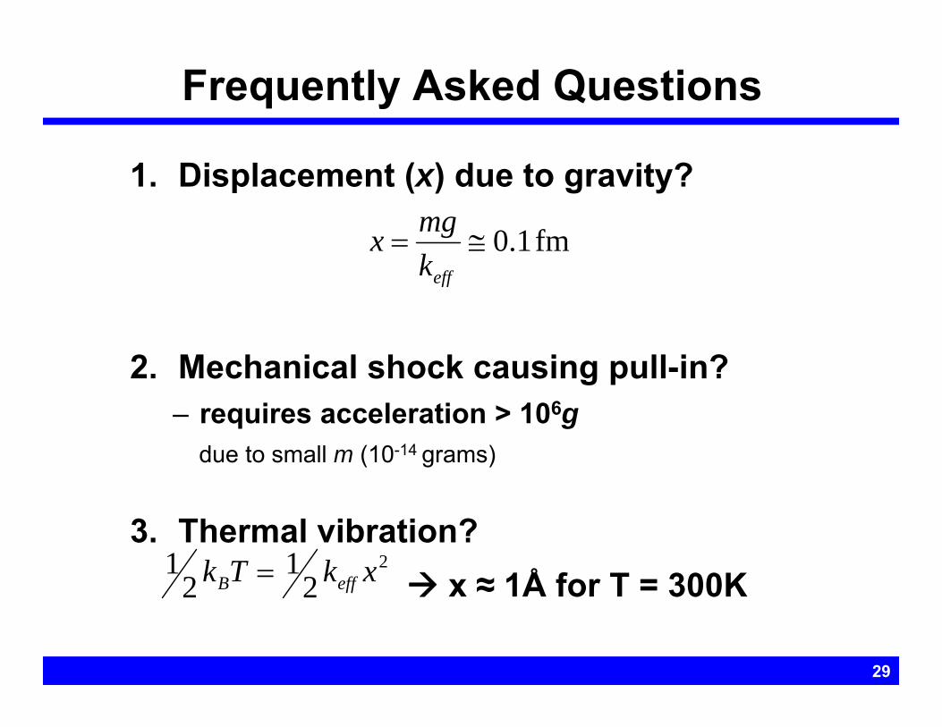
Frequently Asked Questions
1. Displacement (x) due to gravity?
2. Mechanical shock causing pull-in?‒ requires acceleration > 106g
due to small m (10-14 grams)
3. Thermal vibration? x ≈ 1Å for T = 300K
29
fm 1.0effk
mgx
2
21
21 xkTk effB
Related Documents