-1- Masateru Koide May 31, 2012 62 nd ECTC – San Diego, CA: May 29 – June 1, 2012 The Low Warpage Coreless Substrate for High Speed Large Size Die Packages Masateru Koide Device Packaging Technology Dept. Fujitsu Advanced Technology Ltd.

Welcome message from author
This document is posted to help you gain knowledge. Please leave a comment to let me know what you think about it! Share it to your friends and learn new things together.
Transcript

-1- Masateru Koide May 31, 2012
62nd ECTC – San Diego, CA: May 29 – June 1, 2012
The Low Warpage Coreless Substrate
for High Speed Large Size Die Packages
Masateru Koide
Device Packaging Technology Dept.
Fujitsu Advanced Technology Ltd.

-2- Masateru Koide May 31, 2012
AGENDA
1. Introduction
2. Targets of Development
3. Warpage Control Method Development
1. Coreless Substrate
2. Package Assembly
3. Board Mounting
4. Conclusion
-3- Masateru Koide May 31, 2012
1. Introduction
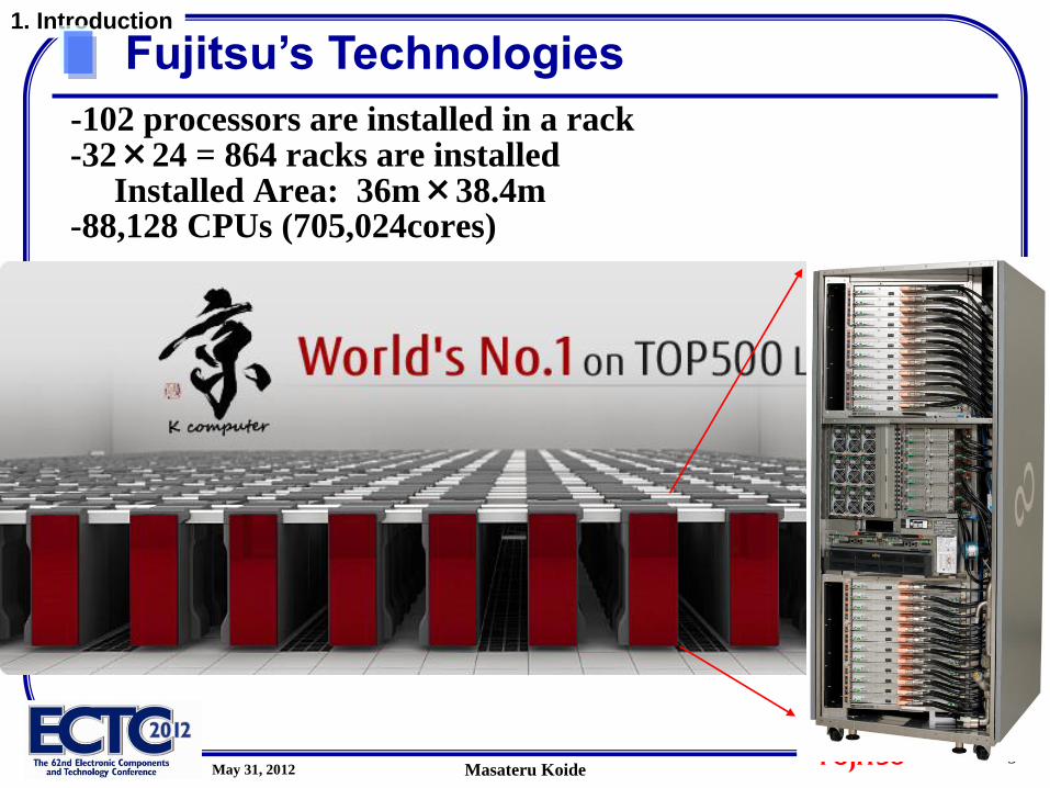
-102 processors are installed in a rack -32×24 = 864 racks are installed Installed Area: 36m×38.4m -88,128 CPUs (705,024cores)
Fujitsu’s Technologies

-4- Masateru Koide May 31, 2012
1. Introduction
Rank Site Computer/Year Vendor Cores Rmax
[Pflops]
Power
[MW]
1 RIKEN Advanced Institute for Computational
Science(AICS)
Japan
K computer, SPARC64 VIIIfx 2.0GHz, Tofu interconnect
/ 2011
Fujitsu
705,024 10.510 12.660
2 National Supercomputing Center In Tianjin
China
Tianhe-1A - NUDT TH MPP, X5670 2.93Ghz 6C,
NVIDIA GPU, FT-1000 8C / 2010
NUDT
186,368 2.566 4.040
3 DOE/SC/Oak Ridge National Laboratory
United States
Jaguar - Cray XT5-HE Opteron 6-core 2.6 GHz / 2009
Cray Inc. 224,162 1.759 6.951
4 National Supercomputing Centre in Shenzhen
(NSCS)
China
Nebulae - Dawning TC3600 Blade, Intel X5650, NVidia
Tesla C2050 GPU / 2010
Dawning
120,640 1.271 2.580
5 GSIC Center, Tokyo Institute of Technology
Japan
TSUBAME 2.0 - HP ProLiant SL390s G7 Xeon 6C X5670,
Nvidia GPU, Linux/Windows / 2010
NEC/HP
73,278 1.192 1.398
6 DOE/NNSA/LANL/SNL
United States
Cielo- Cray XE6 8-core 2.4GHz / 2011
Cray Inc. 142,272 1.110 3.980
7 NASA/Ames Research Center/NAS
United States
Pleiades - SGI Altix ICE 8200EX/8400EX, Xeon HT QC
3.0/Xeon 5570/5670 2.93 Ghz, Infiniband / 2011
SGI
111,104 1.088 4.102
8 DOE/SC/LBNL/NERSC
United States
Hopper - Cray XE6 12-core 2.1 GHz / 2010
Cray Inc. 153,408 1.054 2.910
9 Commissariat a l'Energie Atomique (CEA)
France
Tera-100 - Bull bullx super-node S6010/S6030 / 2010
Bull SA 138,368 1.050 4.590
10 DOE/NNSA/LANL
United States
Roadrunner - BladeCenter QS22/LS21 Cluster,
PowerXCell 8i 3.2 Ghz / Opteron DC 1.8 GHz, Voltaire
Infiniband / 2009
IBM
122,400 1.042 2.346
Efficiency ratio93.2% / 88,128CPU
Super Computer Ranking
Source : 37th TOP500LIST (www.top500.org)
-5- Masateru Koide May 31, 2012
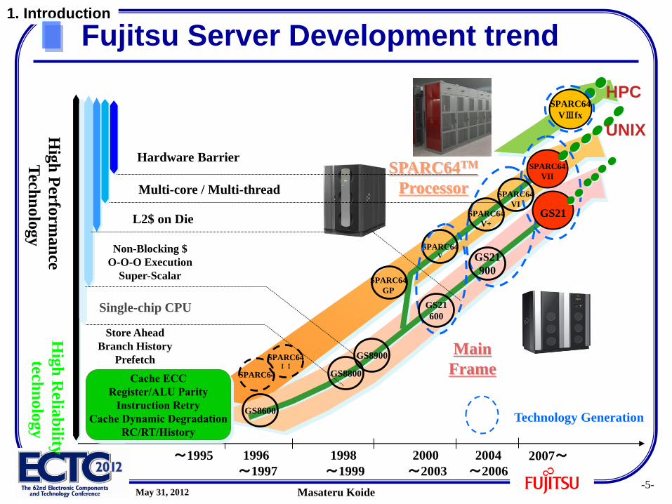
1. Introduction
Hig
h P
erform
an
ce
Tech
nolo
gy
2004
~2006
2000
~2003
1998
~1999
1996
~1997
~1995
SPARC64
SPARC64 II
SPARC64 V
SPARC64
GP
Hig
h R
eliab
ility
techn
olo
gy
GS8900
GS8800
GS8600
Store Ahead
Branch History
Prefetch
Single-chip CPU
Non-Blocking $
O-O-O Execution
Super-Scalar
L2$ on Die
SPARC64
VII
GS21
600
Technology Generation
SPARC64TM
Processor
Main
Frame
SPARC64
V+
SPARC64
VI
GS21
900
GS21
Multi-core / Multi-thread
2007~
Hardware Barrier
SPARC64
VⅢfx
HPC
UNIX
Fujitsu Server Development trend
-6- Masateru Koide May 31, 2012
1. Introduction
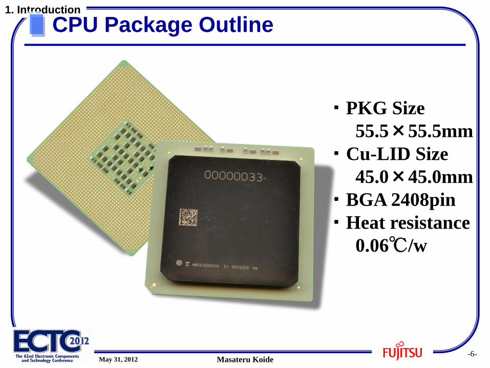
・PKG Size
55.5×55.5mm
・Cu-LID Size
45.0×45.0mm
・BGA 2408pin
・Heat resistance
0.06℃/w
CPU Package Outline
-7- Masateru Koide May 31, 2012
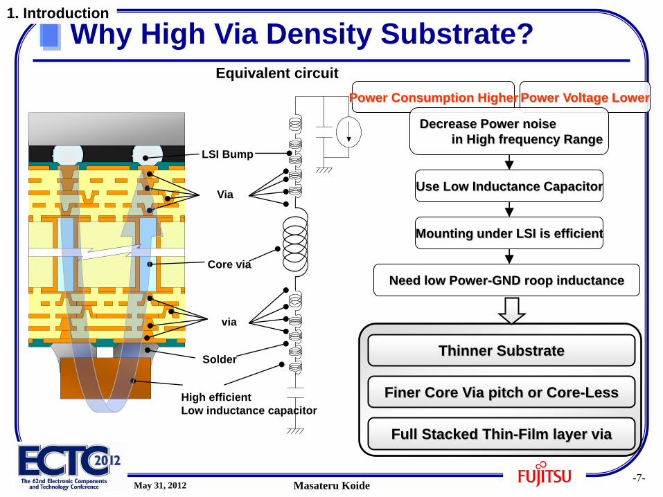
High efficient
Low inductance capacitor
Equivalent circuit
via
Core via
Via
LSI Bump
Solder
Power Consumption Higher Power Voltage Lower
Decrease Power noise
in High frequency Range
Use Low Inductance Capacitor
Mounting under LSI is efficient
Need low Power-GND roop inductance
Thinner Substrate
Finer Core Via pitch or Core-Less
Full Stacked Thin-Film layer via
Why High Via Density Substrate? 1. Introduction

-8- Masateru Koide May 31, 2012
The factors of Warpage 1) CTE mismatch and Low Young’s modulus of package substrate material 2) Package assembly technique 3) Board mount reflow temperature
Coreless Issue 2. Targets of Development
Why is not Coreless popular?
Warpage Control Issue
Cost Miniaturization Inductance Assembly
Coreless
Conventional

-9- Masateru Koide May 31, 2012
Warpage control technique 1. Coreless Substrate Structure Material composition and Structure control 2. Package Assembly Warpage Correction control 3. Board mounting Reflow Temperature control
Development Target 2. Targets of Development
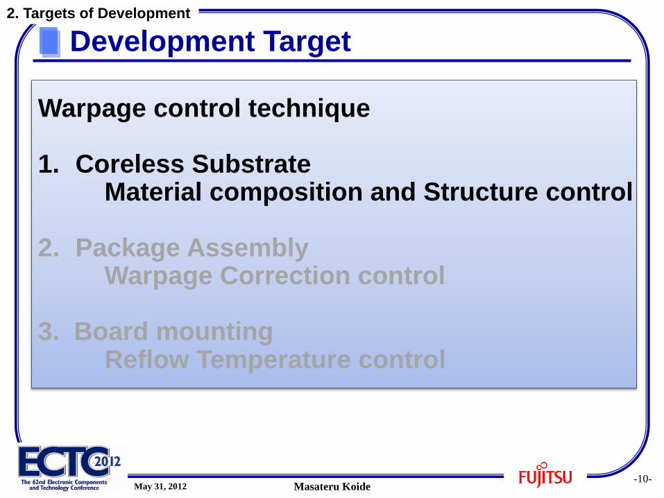
-10- Masateru Koide May 31, 2012
Warpage control technique 1. Coreless Substrate Material composition and Structure control 2. Package Assembly Warpage Correction control 3. Board mounting Reflow Temperature control
Development Target 2. Targets of Development

-11- Masateru Koide May 31, 2012
Using an insulating material with a small CTE mismatch
Cu = 17ppm/ C Resin = 35ppm/ C
General Material Combination
Cu = 17ppm/ C Prepreg = 15ppm/ C
CTE mismatch decreased to 1/9 by prepreg application.
Coreless substrate with all prepreg layers
exhibits smaller warpage
Our Material Combination
° °
° °
3. Experimental Methods
We use prepregs
Warpage Improvement Method

-12- Masateru Koide May 31, 2012
Necessary to reduce the prepreg consumption as much
as possible, and to control a warpage.
Properties Prepreg Resin
CTE(@R.T.) 15ppm/ C 35ppm/ C
CTE mismatch with Cu Small Large
Warpage Exellent Poor
Transmission Property Poor Exellent
° °
3. Experimental Methods
Coreless substrate with all prepreg layers
is inferior to transmission property.
Problem of Prepreg in Transmission
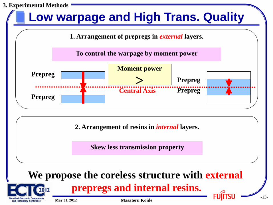
-13- Masateru Koide May 31, 2012
We propose the coreless structure with external
prepregs and internal resins.
1. Arrangement of prepregs in external layers.
To control the warpage by moment power
2. Arrangement of resins in internal layers.
Skew less transmission property
3. Experimental Methods
> Moment power
Prepreg
Prepreg
Prepreg
Prepreg Central Axis
Low warpage and High Trans. Quality
-14- Masateru Koide May 31, 2012
PP layer
Resin layer
Small CTE
mismatch
Large CTE
mismatch
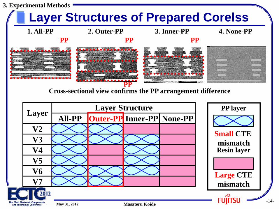
All-PP Outer-PP Inner-PP None-PP
V2
V3
V4
V5
V6
V7
Layer StructureLayer
1. All-PP 2. Outer-PP 3. Inner-PP 4. None-PP
3. Experimental Methods
PP PP
PP
PP
Cross-sectional view confirms the PP arrangement difference
Layer Structures of Prepared Corelss

-15- Masateru Koide May 31, 2012
We succeeded in reducing the warpage
with Outer-PP structure.
115 58 122 307
4. Results
Minimum Warpage
All-PP Outer-PP Inner-PP None-PP
Warpage
(mm) 0 260 130
Warpage Measurement Results
-16- Masateru Koide May 31, 2012
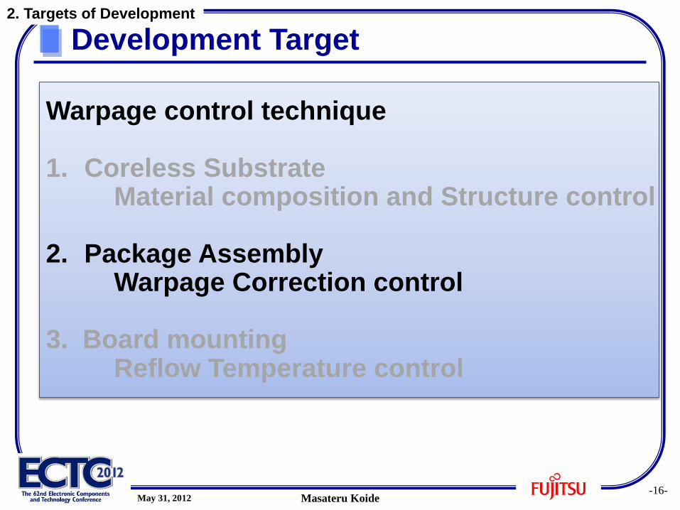
Warpage control technique 1. Coreless Substrate Material composition and Structure control 2. Package Assembly Warpage Correction control 3. Board mounting Reflow Temperature control
Development Target 2. Targets of Development

-17- Masateru Koide May 31, 2012
0
20
40
60
80
100
120
140
Conventional Thincore Coreless
Fig.1 Comparison of LSI area warpage in Each substrate type
実装
エリ
ア反
り [
μm
/□
20m
m]
Average
Same as conventional
Too Large!
LS
I A
rea
Wa
rpag
e [
um
/20
Sq
.mm
]
3.2 Package Assembly
Package Substrate Warpage
-18- Masateru Koide May 31, 2012
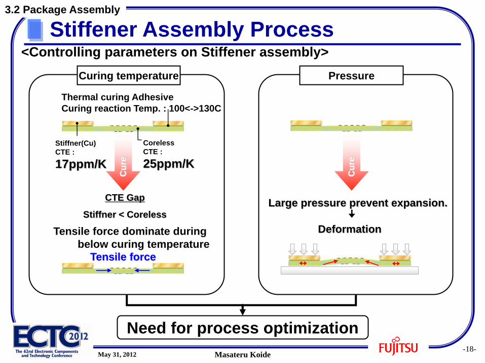
<Controlling parameters on Stiffener assembly>
Need for process optimization
Coreless
CTE :
25ppm/K
Curing temperature
Cu
re
Stiffner(Cu)
CTE :
17ppm/K
Thermal curing Adhesive
Curing reaction Temp. : 100<->130C
CTE Gap
Stiffner < Coreless
Tensile force
Cu
re
Pressure
Large pressure prevent expansion.
Tensile force dominate during
below curing temperature
Deformation
Stiffener Assembly Process 3.2 Package Assembly
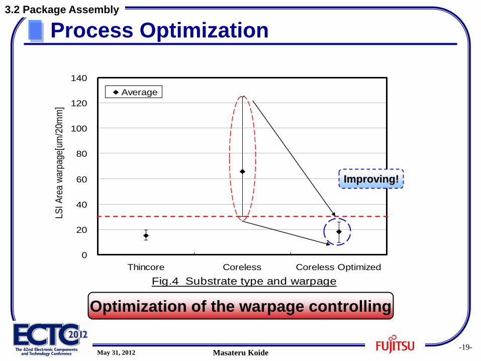
-19- Masateru Koide May 31, 2012
0
20
40
60
80
100
120
140
Thincore Coreless Coreless Optimized
Fig.4 Substrate type and warpage
LS
I A
rea w
arp
age[u
m/2
0m
m]
Average
Optimization of the warpage controlling
Improving!
Process Optimization 3.2 Package Assembly

-20- Masateru Koide May 31, 2012
Reliability Test Result Test conditions
Less than twice of the initial resistance
20 test pieces were prepared
Test results
Effective factors for reliability
1. The warpage value at maximum
temperature
2. The temperature dependent
warpage in cooling process.
Pass conditions
Thermal Cycle -25/+125(cel) 1,000cycles
LSI Size 20mm square, 0.15mm thick
Substrate Size 42.5mm square, 0.3mm thick
1000cycle
Reliability TestAll-PP Passed
Outer-PP PassedInner-PP FailedNone-PP Failed
Sample
3.2 Package Assembly
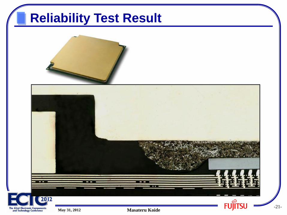
-21- Masateru Koide May 31, 2012
Reliability Test Result

-22- Masateru Koide May 31, 2012
Warpage control technique 1. Coreless Substrate Material composition and Structure control 2. Package Assembly Warpage Correction control 3. Board mounting Reflow Temperature control
Development Target 2. Targets of Development

-23- Masateru Koide May 31, 2012
3.2 Board Mounting
Reflow Temperature
Adopting Low-Temperature Soldering
0
50
100
150
0 50 100 150 200 250 300
Temperuture(cel)
War
page
(mic
ron)
SnBi
Warpage reduction →1/2
SnAgCu
Warp
age
-24- Masateru Koide May 31, 2012
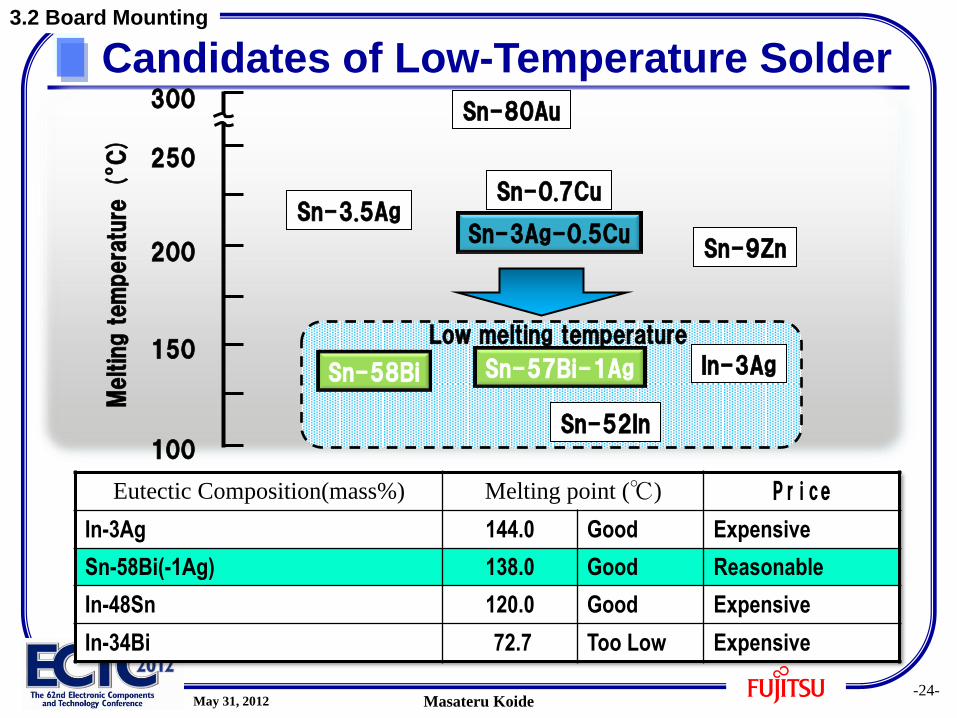
Candidates of Low-Temperature Solder
Eutectic Composition(mass%) Melting point (℃) Price
In-3Ag 144.0 Good Expensive
Sn-58Bi(-1Ag) 138.0 Good Reasonable
In-48Sn 120.0 Good Expensive
In-34Bi 72.7 Too Low Expensive
Sn-0.7Cu Sn-3.5Ag
Sn-9Zn
Sn-58Bi
Sn-52In 100
150
200
250
300 M
eltin
g t
em
pera
ture
(ºC)
Sn-3Ag-0.5Cu
Sn-80Au
Low melting temperature
Sn-57Bi-1Ag In-3Ag
3.2 Board Mounting
-25- Masateru Koide May 31, 2012
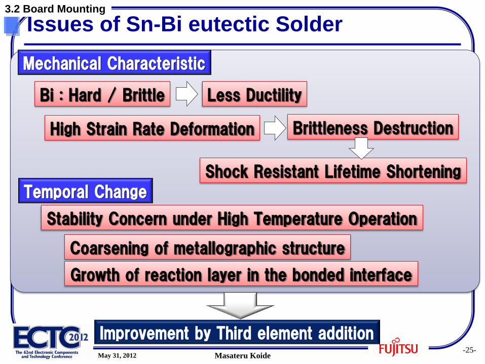
Issues of Sn-Bi eutectic Solder
Temporal Change
Mechanical Characteristic
Improvement by Third element addition
Bi : Hard / Brittle Less Ductility
High Strain Rate Deformation Brittleness Destruction
Shock Resistant Lifetime Shortening
Stability Concern under High Temperature Operation
Coarsening of metallographic structure
Growth of reaction layer in the bonded interface
3.2 Board Mounting

-26- Masateru Koide May 31, 2012
Charactristic Sn-Bi-Sb-Zn
Texture Miniaturization and Ductility improvement by Sb
10μm
Conventional Sn-Bi Solder
Developed Solder
Bre
akin
g e
longation (
%)
3rd element content(wt%)
Test Temp. : Room Temp.
Strain Speed: 2×10⁻³ /sec
0 1 2 3 4 5 0
10
20
30
40
50 Developed Solder (Sb Added)
Conventional (Ag Added)
3.2 Board Mounting

-27- Masateru Koide May 31, 2012
Charactristic Sn-Bi-Sb-Zn
Inhibition of Bi-rich layer constitution, interfacial reinforcement by Zn
Cu5Zn8
Cu Pad
Cu6Sn5
Cu Pad
Bi
Conventional SnBi Solder
Developed Solder
125℃/1000h
Time(h)
Bum
p P
ull
Str
ength
(N)
Conventional
0 500 1000
15
30
25
5
10 (Sn-58Bi)
(Sn-57Bi-1.0Ag)
(Sn-57Bi-0.5Sb-0.5Zn)
0
Developed Solder
20
スタート チャック プルスタート チャック プルStart Chucking Pull
Joint Reliability was Successfully improved
3.2 Board Mounting
-28- Masateru Koide May 31, 2012
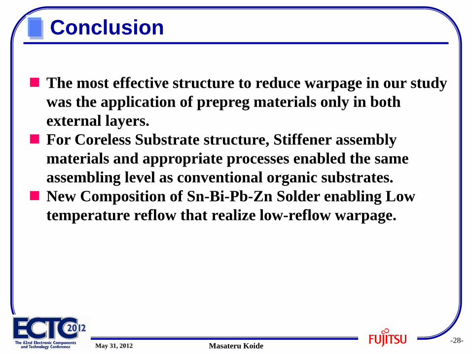
Conclusion
The most effective structure to reduce warpage in our study
was the application of prepreg materials only in both
external layers.
For Coreless Substrate structure, Stiffener assembly
materials and appropriate processes enabled the same
assembling level as conventional organic substrates.
New Composition of Sn-Bi-Pb-Zn Solder enabling Low
temperature reflow that realize low-reflow warpage.
-29- Masateru Koide May 31, 2012
Daisuke Mizutani (Material Analysis)
Mamoru Kurashina (Material Analysis)
Seiki Sakuyama(Material Development)
Kenji Fukuzono (Package Structure Analysis)
Manabu Watanabe(Board Level Reliability)

-30- Masateru Koide May 31, 2012
Related Documents